CN1797954B - Clock signal generating device and method - Google Patents
Clock signal generating device and methodDownload PDFInfo
- Publication number
- CN1797954B CN1797954BCN 200410082021CN200410082021ACN1797954BCN 1797954 BCN1797954 BCN 1797954BCN 200410082021CN200410082021CN 200410082021CN 200410082021 ACN200410082021 ACN 200410082021ACN 1797954 BCN1797954 BCN 1797954B
- Authority
- CN
- China
- Prior art keywords
- delay
- clock signal
- delayed
- signal
- input signal
- Prior art date
- Legal status (The legal status is an assumption and is not a legal conclusion. Google has not performed a legal analysis and makes no representation as to the accuracy of the status listed.)
- Expired - Lifetime
Links
Images


Landscapes
- Stabilization Of Oscillater, Synchronisation, Frequency Synthesizers (AREA)
Abstract
Description
Translated fromChinese技术领域technical field
本发明关于一种时钟信号产生装置及方法,特别是具有校正的时钟信号产生装置及方法。The present invention relates to a clock signal generation device and method, in particular to a clock signal generation device and method with correction.
背景技术Background technique
在数据传输过程中,数据输出与系统时钟信号保持同步相当重要的。然而,当数据或时钟信号经过电路板(PCB)传输时,通常会被耦合(couple)而产生噪声(noise),且信号本身的抖动(jitter),以及电路板上信号线长度的不同所造成的时间差(skew),因此使得较佳锁定(latch)相位缩短,也就是,数据与数据控制信号(DQS)之间的锁定时间会减少。因此,如何产生一个较佳的相位来锁定数据,已成为许多研究人员极力研究方向之一。尤其是在高速应用的电路,此更为一极重要的研究课题。During data transfer, it is very important that the data output is synchronized with the system clock signal. However, when the data or clock signal is transmitted through the circuit board (PCB), it will usually be coupled to generate noise (noise), and the jitter of the signal itself (jitter) and the length of the signal line on the circuit board are different. Therefore, the better locking (latch) phase is shortened, that is, the locking time between the data and the data control signal (DQS) is reduced. Therefore, how to generate a better phase to lock data has become one of the research directions of many researchers. Especially in high-speed application circuits, this is an extremely important research topic.
请参照图1,公知的时钟信号产生系统包括一延迟锁定回路110、一延迟模块120以及一多路转换器130。该延迟锁定回路(Delay lucked loop;DLL)110,其包括一电压控制延迟线(Voltage Controller Delay Line;VCDL)118。其中,该电压控制延迟线118由多个电压控制延迟元件(Delay cell)119串联而成。延迟模块120包括多个电压控制延迟线。当系统时钟信号CKin输入至延迟电路110时,延迟锁定回路110产生一电压控制信号Vc,并且将该电压控制信号Vc施加给延迟模块120的每一电压控制延迟线。组成该延迟模块120的电压控制延迟线的电压控制延迟元件122与延迟锁定回路110中的电压控制延迟元件119相同,即这些电压控制延迟元件119、122对电压控制信号Vc具有相同的特性。如此,系统时钟信号CKin与输出时钟信号CKout保持锁定,进而达到数据输出与系统时钟信号保持同步。Referring to FIG. 1 , a known clock signal generating system includes a delay locked
此外,该延迟锁定回路亦可由一锁相环(Phase lucked loop;PLL)210所取代,如图2所示。参照图2,该时钟信号产生系统包括锁相环(Phase luckedloop;PLL)210、延迟模块220以及多路转换器230。该锁相环210包括一压控振荡器(Voltage Controller Oscillator;VCO)218。In addition, the delay locked loop can also be replaced by a phase locked loop (Phase lucked loop; PLL) 210, as shown in FIG. 2 . Referring to FIG. 2 , the clock signal generating system includes a phase locked loop (Phase lucky loop; PLL) 210, a delay module 220 and a multiplexer 230. The PLL 210 includes a voltage-controlled oscillator (Voltage Controller Oscillator; VCO) 218.
然而,无论延迟锁定回路或锁相环均利用电压控制信号来控制延迟元件的延迟时间,因此整个系统需要持续耗电,并且其延迟元件所占的面积也较大。However, both the delay locked loop and the phase locked loop use the voltage control signal to control the delay time of the delay element, so the whole system requires continuous power consumption, and the area occupied by the delay element is relatively large.
发明内容Contents of the invention
鉴于以上的问题,本发明的目的之一在于提供一种时钟信号产生装置及方法,以此解决先前技术所存在的诸多限制与缺点。In view of the above problems, one of the objectives of the present invention is to provide a clock signal generating device and method, so as to solve many limitations and shortcomings of the prior art.
本发明的目的之一在于提供一种时钟信号产生装置及方法,可降低电源消耗量。One of the objectives of the present invention is to provide a clock signal generating device and method, which can reduce power consumption.
本发明的目的之一在于提供一种时钟信号产生装置及方法,以正确锁定数据信号。One of the objectives of the present invention is to provide a clock signal generating device and method to correctly lock data signals.
因此,为达上述目的,本发明公开一种时钟信号产生装置,包括:一延迟电路;一检测装置;以及一延迟模块,以及一第一多路转换器。延迟电路将一第一输入时钟信号延迟一预定相位,以产生一延迟时钟信号。延迟模块连接至检测装置,其包括多个延迟元件,用以产生一个以上的延迟信号。检测装置连接至延迟电路,当延迟模块接收第一输入信号时,检测装置比较延迟时钟信号与延迟信号,以得到延迟时间与预定相位的一相对应关系;而当延迟模块接收第二输入信号时,检测装置则依据相对应关系输出这些延迟信号中之一。所述第一多路转换器连接至该延迟模块,用以根据该系统的模式选择性输出该第一输入信号和该第二输入信号给该延迟模块。Therefore, to achieve the above purpose, the present invention discloses a clock signal generating device, comprising: a delay circuit; a detection device; and a delay module, and a first multiplexer. The delay circuit delays a first input clock signal by a predetermined phase to generate a delayed clock signal. The delay module is connected to the detection device and includes a plurality of delay elements for generating more than one delay signal. The detection device is connected to the delay circuit. When the delay module receives the first input signal, the detection device compares the delayed clock signal with the delay signal to obtain a corresponding relationship between the delay time and the predetermined phase; and when the delay module receives the second input signal , and the detection device outputs one of these delayed signals according to the corresponding relationship. The first multiplexer is connected to the delay module for selectively outputting the first input signal and the second input signal to the delay module according to the mode of the system.
其中,延迟模块产生的延迟信号可具有相同的延迟时间,或者是具有相同的频率而不同的相位。Wherein, the delayed signals generated by the delay module may have the same delay time, or have the same frequency but different phases.
另外,本发明还公开一种时钟信号产生方法,应用于一系统中,包括下列步骤:提供一预定相位的一延迟时钟信号和相位相异的至少一延迟信号;比较延迟时钟信号与延迟信号,以得到一比较结果;以及根据比较结果而得到一延迟相差。根据该系统的模式选择性输出该第一输入信号和该第二输入信号。In addition, the present invention also discloses a method for generating a clock signal, which is applied to a system and includes the following steps: providing a delayed clock signal with a predetermined phase and at least one delayed signal with a different phase; comparing the delayed clock signal with the delayed signal, to obtain a comparison result; and obtain a delay difference according to the comparison result. The first input signal and the second input signal are selectively output according to the mode of the system.
根据本发明的时钟信号产生装置及方法,利用系统空闲时进入系统的校正模式,以执行相位锁定调整程序,进而得到一延迟相位。因此,当数据传输时系统进入工作模式,此时即可根据延迟相位及欲延迟的相位而产生一精准相位或延迟时钟信号,以此能正确锁定数据或输入/输出数据。并且,于调整完后即可将延迟电路关断,以节省电源的消耗。此外,根据本发明的时钟信号产生装置及方法可于一固定时间时即执行一次调整程序,以避免温度对各元件产生影响。According to the clock signal generation device and method of the present invention, the system enters the calibration mode when the system is idle to execute the phase lock adjustment procedure, and then obtain a delayed phase. Therefore, when the system enters the working mode during data transmission, an accurate phase or delayed clock signal can be generated according to the delayed phase and the phase to be delayed, so as to correctly lock data or input/output data. Moreover, the delay circuit can be turned off after the adjustment is completed, so as to save power consumption. In addition, according to the clock signal generation device and method of the present invention, an adjustment procedure can be executed once at a fixed time, so as to avoid the influence of temperature on each element.
并且,延迟模块中包括的延迟元件可为反相器(invcrter),因此,延迟模块的面积可较先前技术约小十倍,如此一来,即可缩小整个装置的尺寸。Moreover, the delay element included in the delay module can be an inverter (invcrter), therefore, the area of the delay module can be about ten times smaller than that of the prior art, so that the size of the entire device can be reduced.
有关本发明的特征与实作,配合附图对最佳实施例详细说明如下。Regarding the features and implementation of the present invention, the preferred embodiments are described in detail as follows in conjunction with the accompanying drawings.
附图说明Description of drawings
图1为说明先前技术的一实施例的时钟信号产生装置的系统结构图;FIG. 1 is a system structure diagram illustrating a clock signal generating device of an embodiment of the prior art;
图2为说明先前技术的另一实施例的时钟信号产生装置的系统结构图;2 is a system structure diagram illustrating a clock signal generating device of another embodiment of the prior art;
图3为说明根据本发明的一实施例的时钟信号产生装置的系统结构图;3 is a system structure diagram illustrating a clock signal generating device according to an embodiment of the present invention;
图4为说明于图3中延迟模块的一实施例的结构图;FIG. 4 is a block diagram illustrating an embodiment of the delay module in FIG. 3;
图5为说明于图3中检测电路的一实施例的结构图;FIG. 5 is a structural diagram illustrating an embodiment of the detection circuit in FIG. 3;
图6为说明于图3中的检测电路的另一实施例的结构图;以及FIG. 6 is a block diagram of another embodiment of the detection circuit illustrated in FIG. 3; and
图7为说明于图3中延迟模块的另一实施例的结构图。FIG. 7 is a structural diagram illustrating another embodiment of the delay module in FIG. 3 .
主要元件符号说明Explanation of main component symbols
110 延迟锁定回路110 Delay locked loop
112 相位检测器112 Phase detector
114 电流泵114 Current pump
116 低通滤波器116 low pass filter
118 电压控制延迟线118 Voltage controlled delay line
119 电压控制延迟元件119 Voltage controlled delay element
120 延迟模块120 delay module
122 电压控制延迟元件122 Voltage controlled delay element
130 多路转换器130 Multiplexer
210 锁相环210 phase locked loop
212 相位检测器212 phase detector
214 电流泵214 Current pump
216 低通滤波器216 low pass filter
217 分频装置217 Frequency divider
218 压控振荡器218 Voltage Controlled Oscillator
220 延迟模块220 delay module
222 电压控制延迟元件222 Voltage controlled delay element
230 多路转换器230 Multiplexer
310 延迟电路310 delay circuit
320 延迟模块320 delay module
322 延迟线322 delay line
323 延迟元件323 delay element
330 第一多路转换器330 First multiplexer
340 检测电路340 detection circuit
342 比较器342 Comparator
344 第一控制器344 The first controller
345 第二控制器345 Second controller
346 第二多路转换器346 Second multiplexer
CKa 延迟时钟信号CKa Delayed clock signal
CKf 反馈信号CKf feedback signal
CKin 第一输入时钟信号CKin The first input clock signal
CKDDR 第二输入时钟信号CKDDR second input clock signal
CKout 输出时钟信号CKout Output clock signal
D1-Dk-Dn 延迟信号D1-Dk-Dn delayed signal
P 相位差信号P Phase difference signal
Vc 电压控制信号Vc Voltage control signal
具体实施方式Detailed ways
本发明的一实施例如图3所示。于本实施例中,时钟信号产生装置包括:一延迟电路310、一延迟模块320以及一检测电路340。An embodiment of the present invention is shown in FIG. 3 . In this embodiment, the clock signal generating device includes: a
延迟电路310接收第一输入时钟信号CKin并产生一已知相位差的延迟时钟信号CKa,即将第一输入时钟信号CKin延迟一预定相位,以产生延迟时钟信号CKa。于此,该延迟电路310可为一延迟锁定回路(DLL)亦可为一锁相环(PLL),或是其他可延迟一已知相位差的装置。而此第一输入时钟信号CKin可为一系统时钟信号。The
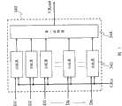
延迟模块320由多个数字延迟线322所构成,其每一数字延迟线322分别由至少一延迟元件323所组成,如图4所示。于此,延迟模块320可产生多个延迟信号D1-Dn,然后输入至检测装置340,其中,每一延迟信号D1-Dn的延迟时间皆不同,但每一延迟元件323的延迟时间相同。于此,延迟元件323可为任意能产生延迟的元件或逻辑单元或其组合,较常使用的元件是反相器。The
检测装置340用以比较延迟时钟信号CKa与延迟信号D1-Dn,以得到延迟时间与预定相位的相对应关系,并依据相对应关输出一输出时钟信号CKout。其中,该检测装置340包括多个比较器342以及一第一控制器344,如图5所示。于此,延迟信号D1-Dn分别输入至相对应的比较器342中,此时,比较器342分别比较每一延迟信号D1-Dn与延迟时钟信号CKa,进而得知每一延迟元件323的延迟时间与延迟时钟信号CKa的已知相位差的相对关系,因而,第一第一控制器344即可藉由得知的相对关系而输出适当的输出时钟信号CKout。The
并且,于该实施例中,该时钟信号产生装置还包括:一第一多路转换器330,用以接收一第一输入时钟信号CKin和一第二输入时钟信号CKDDR,并选择性输出第一输入时钟信号CKin和第二输入时钟信号CKDDR给延迟模块320。换句话说,在该实施例中,该时钟信号产生装置的操作模式可分为一工作模式与一校正模式,当于校正模式时,第一多路转换器330选择第一输入时钟信号CKin输入至延迟模块320;而于工作模式时,第一多路转换器330则选择第二输入时钟信号CKDDR输入至延迟模块320。Moreover, in this embodiment, the clock signal generating device further includes: a
具体来说,请参照第3-5图,当根据本发明一实施例的时钟信号产生装置于校正模式时,延迟电路310依据第一输入时钟信号CKin而产生一延迟相位差为90度的延迟时钟信号CKa,而第一多路转换器330将第一输入时钟信号CKin输入至延迟模块320。此时,第一输入时钟信号CKin经由延迟模块320内各个延迟线322的作用而产生n个延迟信号D1-Dn。而检测电路340内n个比较器342分别比较延迟参考时钟信号CKa与延迟信号D1-Dn,而得到第k个延迟信号Dk的相位最接近延迟时钟信号CKa的相位,进而可得知每一延迟元件323的延迟时间与延迟时钟信号CKa的已知相位差的相对关系。此时,当于工作模式下,第一多路转换器330将第二输入时钟信号CKDDR输入至延迟模块320,而第一控制器344可藉由上述的相对关系而输出适当的输出时钟信号CKout。也就是,若假定k为10,即比较后得到第10个延迟信号D10的相位最接近延迟时钟信号的相位,而由于延迟时钟信号相差90度,因此得到每一延迟元件342会延迟9度的相位。于工作模式下,假定该输出时钟信号需延迟相位36度时,此时,第一控制器344则输出第四数字延迟线经由延迟第二输入时钟信号CKDDR36度(9度×4)的延迟相位而产生的时钟信号。Specifically, please refer to FIGS. 3-5. When the clock signal generating device according to an embodiment of the present invention is in the correction mode, the
此外,延迟模块320的另一实施例如图6所示,其包括一延迟线322。该延迟线322由多个延迟元件323彼此串接而成,其中,当延迟线322延迟一输入时钟信号(即,第一输入时钟信号CKin或第二输入时钟信号CKDDR)时,每一延迟元件会分别输出一延迟信号,而形成上述的延迟信号D1-Dn。并且,每一延迟信号的频率相同,而其相位不同。同样,该延迟元件323可为任意能产生延迟的元件或逻辑单元或其组合,较常使用的元件是反相器。In addition, another embodiment of the
此外,检测装置340的另一实施例如图6所示,其包括:一第二多路转换器346、一比较器342、以及一第二控制器345。参照图7,于第二多路转换器346用以接收延迟信号D1-Dn,并依据来自第二控制器345的一选择信号SS而选择延迟信号D1-Dn中的一延迟信号,并将其输出至比较器342。此时,比较器342依次比较输入的延迟信号与延迟时钟信号CKa,并依次输出比较结果至第二控制器345。而第二控制器345会依据比较结果输出一输出时钟信号CKout。In addition, another embodiment of the
并且,上述的时钟信号产生装置利用系统空闲时执行相位锁定调整(此时即为校正模式),并且于调整完后即可将延迟电路关断,即完成于校正模式后将延迟电路关断,进而能降低电源的消耗量。Moreover, the above-mentioned clock signal generating device performs phase lock adjustment when the system is idle (at this time, it is the calibration mode), and the delay circuit can be turned off after the adjustment is completed, that is, the delay circuit is turned off after the calibration mode is completed, Furthermore, power consumption can be reduced.
综合以上所述,本发明亦公开一种时钟信号产生方法,包括下列步骤:提供一预定相位的一延迟时钟信号;提供多个延迟信号;比较延迟时钟信号与延迟信号以得到一比较结果;以及根据比较结果选择输出一输出时钟信号。Based on the above, the present invention also discloses a method for generating a clock signal, comprising the following steps: providing a delayed clock signal with a predetermined phase; providing a plurality of delayed signals; comparing the delayed clock signal with the delayed signal to obtain a comparison result; and An output clock signal is selected and output according to the comparison result.
另外,本发明所公开的产生精准时钟信号的调整装置及方法除了应用于双数据传送率(DDR)存储器之外,尚可应用于其他种类的存储器装置或者其他时序的电子装置。In addition, the adjustment device and method for generating a precise clock signal disclosed in the present invention can be applied to other types of memory devices or electronic devices with other timings besides double data transfer rate (DDR) memory.
本发明虽以优选实施例公开如上,然其并非用以限定本发明,任何本领域技术人员,在不脱离本发明的精神和范围的情况下,可进行更动与修改,因此本发明的保护范围以所提出的权利要求所限定的范围为准。Although the present invention is disclosed as above with preferred embodiments, it is not intended to limit the present invention. Any person skilled in the art can make changes and modifications without departing from the spirit and scope of the present invention. Therefore, the protection of the present invention The scope is as defined by the appended claims.
Claims (9)
Translated fromChinesePriority Applications (1)
| Application Number | Priority Date | Filing Date | Title |
|---|---|---|---|
| CN 200410082021CN1797954B (en) | 2004-12-22 | 2004-12-22 | Clock signal generating device and method |
Applications Claiming Priority (1)
| Application Number | Priority Date | Filing Date | Title |
|---|---|---|---|
| CN 200410082021CN1797954B (en) | 2004-12-22 | 2004-12-22 | Clock signal generating device and method |
Publications (2)
| Publication Number | Publication Date |
|---|---|
| CN1797954A CN1797954A (en) | 2006-07-05 |
| CN1797954Btrue CN1797954B (en) | 2010-09-08 |
Family
ID=36818781
Family Applications (1)
| Application Number | Title | Priority Date | Filing Date |
|---|---|---|---|
| CN 200410082021Expired - LifetimeCN1797954B (en) | 2004-12-22 | 2004-12-22 | Clock signal generating device and method |
Country Status (1)
| Country | Link |
|---|---|
| CN (1) | CN1797954B (en) |
Cited By (1)
| Publication number | Priority date | Publication date | Assignee | Title |
|---|---|---|---|---|
| TWI820963B (en)* | 2022-10-12 | 2023-11-01 | 乾瞻科技股份有限公司 | Data input apparatus and processing method for input data |
Families Citing this family (1)
| Publication number | Priority date | Publication date | Assignee | Title |
|---|---|---|---|---|
| CN101526830B (en)* | 2008-03-07 | 2011-05-11 | 瑞昱半导体股份有限公司 | Clock signal generation circuit and digital circuit with this circuit |
Citations (2)
| Publication number | Priority date | Publication date | Assignee | Title |
|---|---|---|---|---|
| CN1302477A (en)* | 1999-04-27 | 2001-07-04 | 精工爱普生株式会社 | Clock generation circuit, serial/parallel converter and parallel/serial converter and semiconductor device |
| US20040210414A1 (en)* | 2003-03-26 | 2004-10-21 | Peter Gregorius | Method for measuring the delay time of a signal line |
- 2004
- 2004-12-22CNCN 200410082021patent/CN1797954B/ennot_activeExpired - Lifetime
Patent Citations (2)
| Publication number | Priority date | Publication date | Assignee | Title |
|---|---|---|---|---|
| CN1302477A (en)* | 1999-04-27 | 2001-07-04 | 精工爱普生株式会社 | Clock generation circuit, serial/parallel converter and parallel/serial converter and semiconductor device |
| US20040210414A1 (en)* | 2003-03-26 | 2004-10-21 | Peter Gregorius | Method for measuring the delay time of a signal line |
Cited By (1)
| Publication number | Priority date | Publication date | Assignee | Title |
|---|---|---|---|---|
| TWI820963B (en)* | 2022-10-12 | 2023-11-01 | 乾瞻科技股份有限公司 | Data input apparatus and processing method for input data |
Also Published As
| Publication number | Publication date |
|---|---|
| CN1797954A (en) | 2006-07-05 |
Similar Documents
| Publication | Publication Date | Title |
|---|---|---|
| JP4774340B2 (en) | DLL having a function of periodically performing a locking operation during power-down mode and a locking operation method thereof | |
| KR100338212B1 (en) | Dual loop delay-locked loop | |
| JP3404369B2 (en) | DLL circuit | |
| US20020079937A1 (en) | Digital delay locked loop with wide dynamic range and fine precision | |
| US7782103B2 (en) | Phase adjustment circuit | |
| US8242822B2 (en) | Delay locked loop | |
| KR100894255B1 (en) | Delay locked loops, integrated circuits comprising the same and methods of driving the same | |
| US8698533B2 (en) | Phase mixer with adjustable load-to-drive ratio | |
| JP2010193493A (en) | Initialization circuit for delay locked loop | |
| JP4390353B2 (en) | Clock generation method and clock generation circuit | |
| KR20080001432A (en) | Duty cycle correction circuit and delay locked loop circuit | |
| JP2010093771A (en) | Dll circuit | |
| CN103684435A (en) | Delay Line Circuit, Delay Locked Loop and Its Test System | |
| US8026749B2 (en) | Phase locked loop circuit, method of operating phase locked loop circuit and semiconductor memory device including phase locked loop circuit | |
| KR100400041B1 (en) | Method and DLL(Delay Locked Loop) with controlling phase precisely | |
| US7605624B2 (en) | Delay locked loop (DLL) circuit for generating clock signal for memory device | |
| US6967536B2 (en) | Phase-locked loop circuit reducing steady state phase error | |
| US8446197B2 (en) | Delay locked loop and method for driving the same | |
| US7453297B1 (en) | Method of and circuit for deskewing clock signals in an integrated circuit | |
| US7279944B2 (en) | Clock signal generator with self-calibrating mode | |
| US20070152715A1 (en) | Locked loop circuit for improving locking speed and clock locking method using the same | |
| US20070086555A1 (en) | DLL circuit having two input standard clocks, clock signal generation circuit having the DLL circuit and clock signal generation method | |
| CN1797954B (en) | Clock signal generating device and method | |
| CN117713807A (en) | Delay phase-locked loop circuit and multi-phase clock signal duty cycle adjustment method | |
| KR20050011586A (en) | Delay Locked Loop For Generating Multi-Phase Clocks Without Voltage-Controlled Oscillator |
Legal Events
| Date | Code | Title | Description |
|---|---|---|---|
| C06 | Publication | ||
| PB01 | Publication | ||
| C10 | Entry into substantive examination | ||
| SE01 | Entry into force of request for substantive examination | ||
| C14 | Grant of patent or utility model | ||
| GR01 | Patent grant | ||
| CX01 | Expiry of patent term | Granted publication date:20100908 | |
| CX01 | Expiry of patent term |