CN1797144B - Coplanar Switching Mode Liquid Crystal Display Devices - Google Patents
Coplanar Switching Mode Liquid Crystal Display DevicesDownload PDFInfo
- Publication number
- CN1797144B CN1797144BCN2005100767813ACN200510076781ACN1797144BCN 1797144 BCN1797144 BCN 1797144BCN 2005100767813 ACN2005100767813 ACN 2005100767813ACN 200510076781 ACN200510076781 ACN 200510076781ACN 1797144 BCN1797144 BCN 1797144B
- Authority
- CN
- China
- Prior art keywords
- electrode
- pixel
- data
- horizontal
- switching device
- Prior art date
- Legal status (The legal status is an assumption and is not a legal conclusion. Google has not performed a legal analysis and makes no representation as to the accuracy of the status listed.)
- Expired - Fee Related
Links
Images


Classifications
- G—PHYSICS
- G02—OPTICS
- G02F—OPTICAL DEVICES OR ARRANGEMENTS FOR THE CONTROL OF LIGHT BY MODIFICATION OF THE OPTICAL PROPERTIES OF THE MEDIA OF THE ELEMENTS INVOLVED THEREIN; NON-LINEAR OPTICS; FREQUENCY-CHANGING OF LIGHT; OPTICAL LOGIC ELEMENTS; OPTICAL ANALOGUE/DIGITAL CONVERTERS
- G02F1/00—Devices or arrangements for the control of the intensity, colour, phase, polarisation or direction of light arriving from an independent light source, e.g. switching, gating or modulating; Non-linear optics
- G02F1/01—Devices or arrangements for the control of the intensity, colour, phase, polarisation or direction of light arriving from an independent light source, e.g. switching, gating or modulating; Non-linear optics for the control of the intensity, phase, polarisation or colour
- G02F1/13—Devices or arrangements for the control of the intensity, colour, phase, polarisation or direction of light arriving from an independent light source, e.g. switching, gating or modulating; Non-linear optics for the control of the intensity, phase, polarisation or colour based on liquid crystals, e.g. single liquid crystal display cells
- G02F1/133—Constructional arrangements; Operation of liquid crystal cells; Circuit arrangements
- G02F1/1333—Constructional arrangements; Manufacturing methods
- G02F1/1343—Electrodes
- G02F1/134309—Electrodes characterised by their geometrical arrangement
- G02F1/134363—Electrodes characterised by their geometrical arrangement for applying an electric field parallel to the substrate, i.e. in-plane switching [IPS]
- G—PHYSICS
- G02—OPTICS
- G02F—OPTICAL DEVICES OR ARRANGEMENTS FOR THE CONTROL OF LIGHT BY MODIFICATION OF THE OPTICAL PROPERTIES OF THE MEDIA OF THE ELEMENTS INVOLVED THEREIN; NON-LINEAR OPTICS; FREQUENCY-CHANGING OF LIGHT; OPTICAL LOGIC ELEMENTS; OPTICAL ANALOGUE/DIGITAL CONVERTERS
- G02F1/00—Devices or arrangements for the control of the intensity, colour, phase, polarisation or direction of light arriving from an independent light source, e.g. switching, gating or modulating; Non-linear optics
- G02F1/01—Devices or arrangements for the control of the intensity, colour, phase, polarisation or direction of light arriving from an independent light source, e.g. switching, gating or modulating; Non-linear optics for the control of the intensity, phase, polarisation or colour
- G02F1/13—Devices or arrangements for the control of the intensity, colour, phase, polarisation or direction of light arriving from an independent light source, e.g. switching, gating or modulating; Non-linear optics for the control of the intensity, phase, polarisation or colour based on liquid crystals, e.g. single liquid crystal display cells
- G02F1/133—Constructional arrangements; Operation of liquid crystal cells; Circuit arrangements
- G02F1/136—Liquid crystal cells structurally associated with a semi-conducting layer or substrate, e.g. cells forming part of an integrated circuit
- G02F1/1362—Active matrix addressed cells
- G02F1/13624—Active matrix addressed cells having more than one switching element per pixel
- G—PHYSICS
- G09—EDUCATION; CRYPTOGRAPHY; DISPLAY; ADVERTISING; SEALS
- G09G—ARRANGEMENTS OR CIRCUITS FOR CONTROL OF INDICATING DEVICES USING STATIC MEANS TO PRESENT VARIABLE INFORMATION
- G09G3/00—Control arrangements or circuits, of interest only in connection with visual indicators other than cathode-ray tubes
- G09G3/20—Control arrangements or circuits, of interest only in connection with visual indicators other than cathode-ray tubes for presentation of an assembly of a number of characters, e.g. a page, by composing the assembly by combination of individual elements arranged in a matrix no fixed position being assigned to or needed to be assigned to the individual characters or partial characters
- G09G3/34—Control arrangements or circuits, of interest only in connection with visual indicators other than cathode-ray tubes for presentation of an assembly of a number of characters, e.g. a page, by composing the assembly by combination of individual elements arranged in a matrix no fixed position being assigned to or needed to be assigned to the individual characters or partial characters by control of light from an independent source
- G09G3/36—Control arrangements or circuits, of interest only in connection with visual indicators other than cathode-ray tubes for presentation of an assembly of a number of characters, e.g. a page, by composing the assembly by combination of individual elements arranged in a matrix no fixed position being assigned to or needed to be assigned to the individual characters or partial characters by control of light from an independent source using liquid crystals
- G09G3/3611—Control of matrices with row and column drivers
- G09G3/3648—Control of matrices with row and column drivers using an active matrix
- G09G3/3659—Control of matrices with row and column drivers using an active matrix the addressing of the pixel involving the control of two or more scan electrodes or two or more data electrodes, e.g. pixel voltage dependant on signal of two data electrodes
- G—PHYSICS
- G02—OPTICS
- G02F—OPTICAL DEVICES OR ARRANGEMENTS FOR THE CONTROL OF LIGHT BY MODIFICATION OF THE OPTICAL PROPERTIES OF THE MEDIA OF THE ELEMENTS INVOLVED THEREIN; NON-LINEAR OPTICS; FREQUENCY-CHANGING OF LIGHT; OPTICAL LOGIC ELEMENTS; OPTICAL ANALOGUE/DIGITAL CONVERTERS
- G02F2201/00—Constructional arrangements not provided for in groups G02F1/00 - G02F7/00
- G02F2201/12—Constructional arrangements not provided for in groups G02F1/00 - G02F7/00 electrode
- G02F2201/122—Constructional arrangements not provided for in groups G02F1/00 - G02F7/00 electrode having a particular pattern
- G—PHYSICS
- G02—OPTICS
- G02F—OPTICAL DEVICES OR ARRANGEMENTS FOR THE CONTROL OF LIGHT BY MODIFICATION OF THE OPTICAL PROPERTIES OF THE MEDIA OF THE ELEMENTS INVOLVED THEREIN; NON-LINEAR OPTICS; FREQUENCY-CHANGING OF LIGHT; OPTICAL LOGIC ELEMENTS; OPTICAL ANALOGUE/DIGITAL CONVERTERS
- G02F2201/00—Constructional arrangements not provided for in groups G02F1/00 - G02F7/00
- G02F2201/12—Constructional arrangements not provided for in groups G02F1/00 - G02F7/00 electrode
- G02F2201/124—Constructional arrangements not provided for in groups G02F1/00 - G02F7/00 electrode interdigital
- G—PHYSICS
- G02—OPTICS
- G02F—OPTICAL DEVICES OR ARRANGEMENTS FOR THE CONTROL OF LIGHT BY MODIFICATION OF THE OPTICAL PROPERTIES OF THE MEDIA OF THE ELEMENTS INVOLVED THEREIN; NON-LINEAR OPTICS; FREQUENCY-CHANGING OF LIGHT; OPTICAL LOGIC ELEMENTS; OPTICAL ANALOGUE/DIGITAL CONVERTERS
- G02F2201/00—Constructional arrangements not provided for in groups G02F1/00 - G02F7/00
- G02F2201/40—Arrangements for improving the aperture ratio
- G—PHYSICS
- G09—EDUCATION; CRYPTOGRAPHY; DISPLAY; ADVERTISING; SEALS
- G09G—ARRANGEMENTS OR CIRCUITS FOR CONTROL OF INDICATING DEVICES USING STATIC MEANS TO PRESENT VARIABLE INFORMATION
- G09G2300/00—Aspects of the constitution of display devices
- G09G2300/08—Active matrix structure, i.e. with use of active elements, inclusive of non-linear two terminal elements, in the pixels together with light emitting or modulating elements
- G09G2300/0809—Several active elements per pixel in active matrix panels
Landscapes
- Physics & Mathematics (AREA)
- Nonlinear Science (AREA)
- General Physics & Mathematics (AREA)
- Chemical & Material Sciences (AREA)
- Crystallography & Structural Chemistry (AREA)
- Mathematical Physics (AREA)
- Optics & Photonics (AREA)
- Engineering & Computer Science (AREA)
- Geometry (AREA)
- Computer Hardware Design (AREA)
- Theoretical Computer Science (AREA)
- Microelectronics & Electronic Packaging (AREA)
- Liquid Crystal (AREA)
- Thin Film Transistor (AREA)
Abstract
Translated fromChineseDescription
Translated fromChinese技术领域technical field
本发明涉及一种共平面开关(IPS)模式液晶显示(LCD)器件,并且尤其涉及一种不具有与相邻的水平电极形成水平电场的公共电极的IPS模式LCD器件。The present invention relates to an in-plane switching (IPS) mode liquid crystal display (LCD) device, and more particularly to an IPS mode LCD device without a common electrode forming a horizontal electric field with adjacent horizontal electrodes.
背景技术Background technique
随着对诸如移动电话、PDA和笔记本电脑等各种便携式电子器件需求的不断增加,对具有轻、薄、短、小特性的平板显示器件的需求也不断增加。As the demand for various portable electronic devices such as mobile phones, PDAs, and notebook computers continues to increase, the demand for flat panel display devices that are light, thin, short, and small is also increasing.
在诸如液晶显示(LCD)器件、等离子体显示板(PDP)、场发射型显示器(FED)、真空荧光显示器(VFD)等平板显示器件中,LCD器件以其大规模的产量、简单的驱动方法和较高的图像质量而得到最普遍的应用。Among flat panel display devices such as liquid crystal display (LCD) devices, plasma display panels (PDP), field emission displays (FED), vacuum fluorescent displays (VFD), etc., LCD devices are And higher image quality and get the most common application.
LCD器件通过使用电场控制液晶的光透射比显示图像,该LCD器件设置有具有以矩阵形式排列的像素的液晶显示板,以及用于驱动液晶显示板的驱动电路。The LCD device displays images by controlling light transmittance of liquid crystals using an electric field, and is provided with a liquid crystal display panel having pixels arranged in a matrix, and a driving circuit for driving the liquid crystal display panel.
图1示出了根据现有技术的IPS模式LCD器件的单位像素。如图1所示,彼此交叉的栅线101和数据线102限定一像素区。作为开关器件的薄膜晶体管(TFT)形成于栅线101和数据线102的交叉处。在液晶显示板的各像素中,像素电极103和公共电极105交替排列。在TFT的沟道由栅极109导通时,像素电极103接收来自TFT源极/漏极106和107的数据信号从而与公共电极在第一基板上形成水平电场。FIG. 1 shows a unit pixel of an IPS mode LCD device according to the prior art. As shown in FIG. 1 , gate lines 101 and data lines 102 crossing each other define a pixel area. A thin film transistor (TFT) as a switching device is formed at the intersection of the gate line 101 and the data line 102 . In each pixel of the liquid crystal display panel, pixel electrodes 103 and common electrodes 105 are arranged alternately. When the channel of the TFT is turned on by the gate 109 , the pixel electrode 103 receives data signals from the TFT source/drain 106 and 107 to form a horizontal electric field on the first substrate with the common electrode.
LCD器件根据施加到各像素电极的数据信号通过在像素电极103和公共电极105之间施加的电场来控制液晶的光透射比以显示图像。The LCD device controls light transmittance of liquid crystals to display images by an electric field applied between the pixel electrodes 103 and the common electrode 105 according to data signals applied to the respective pixel electrodes.
尽管未示出,面向第一基板形成第二基板,即滤色片基板,并且在第一基板和第二基板之间的间隙形成有液晶层。Although not shown, a second substrate, that is, a color filter substrate is formed facing the first substrate, and a liquid crystal layer is formed in a gap between the first substrate and the second substrate.
通过在像素电极103和公共电极105之间形成的水平电场驱动液晶层的液晶分子。因此,IPS模式LCD器件比由扭曲向列模式驱动的LCD器件具有更宽的视角从而获得对应于左右和上下方向大约80~85度的视角。Liquid crystal molecules of the liquid crystal layer are driven by a horizontal electric field formed between the pixel electrode 103 and the common electrode 105 . Therefore, the IPS mode LCD device has a wider viewing angle than an LCD device driven by a twisted nematic mode so as to obtain a viewing angle corresponding to approximately 80˜85 degrees in left and right and up and down directions.
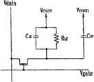
图2所示为IPS模式LCD器件单位像素的电路图。参照图2,在栅线(Vgate)和数据线(Vdata)的交叉部分形成作为开关器件的薄膜晶体管(TFT)。该薄膜晶体管与用于向液晶施加电场的像素电极(未示出)连接。在像素电极和公共电极(Vcom)之间形成水平电场。此外,像素电极、公共电极和具有自阻(RLC)的液晶层形成一电容(CLC)。像素电极、公共电极以及形成在像素电极和公共电极之间的绝缘层进一步形成存储电容(CST),并保持数据信号。Figure 2 shows a circuit diagram of a unit pixel of an IPS mode LCD device. Referring to FIG. 2, a thin film transistor (TFT) as a switching device is formed at a crossing portion of a gate line (Vgate) and a data line (Vdata). The thin film transistor is connected to a pixel electrode (not shown) for applying an electric field to the liquid crystal. A horizontal electric field is formed between the pixel electrode and the common electrode (Vcom). In addition, the pixel electrode, the common electrode and the liquid crystal layer with self-resistance (RLC ) form a capacitor (CLC ). The pixel electrode, the common electrode, and the insulating layer formed between the pixel electrode and the common electrode further form a storage capacitor (CST ), and hold a data signal.
随着LCD器件不断增大,在基板上水平和垂直方向排列的栅线和数据线变长从而增加了线电阻。因此,不能连续驱动形成在栅线上的TFT,该情况称为线路延迟现象。也就是说,即使向一条栅线施加扫描信号,如果该栅线很长,由于线电阻会导致第一TFT和第N TFT接收不同的扫描信号。As LCD devices continue to grow in size, gate lines and data lines arranged horizontally and vertically on a substrate become longer to increase line resistance. Therefore, the TFTs formed on the gate lines cannot be continuously driven, which is called a line delay phenomenon. That is, even if a scan signal is applied to one gate line, if the gate line is long, the first TFT and the Nth TFT receive different scan signals due to line resistance.
同样,由于通过单光掩模工艺不能形成大尺寸的LCD板,需要执行多光掩模工艺来制造LCD板。因此,通过各掩模工艺形成的TFT可能具有不同的特性,这会在各单位像素得到不同的图像质量并降低图像质量。Also, since a large-sized LCD panel cannot be formed through a single photomask process, multiple photomask processes need to be performed to manufacture the LCD panel. Therefore, TFTs formed through each mask process may have different characteristics, which may result in different image quality at each unit pixel and degrade image quality.
并且,在现有的IPS模式LCD器件中,像素电极和公共电极彼此平行设置以施加水平电场。然而,由于公共电极降低了孔径比,将公共电极线邻近于栅线以使像素区最大化。在这个过程中,在栅线和公共电极线之间可能会产生短路。Also, in the existing IPS mode LCD device, the pixel electrode and the common electrode are arranged parallel to each other to apply a horizontal electric field. However, since the common electrode lowers the aperture ratio, the common electrode line is adjacent to the gate line to maximize the pixel area. During this process, a short circuit may be generated between the gate line and the common electrode line.
发明内容Contents of the invention
本发明提供了一种共平面开关(IPS)模式LCD器件,其通过在形成于相邻像素的电极之间形成水平电场而不必构建公共电极来防止由于线路延迟或晶体管之间的不同特性导致的图像质量降低的现象。制造该IPS模式LCD器件的方法包括避免诸如在形成栅线时产生栅线和公共线之间短路问题的简单工艺。The present invention provides an In-Plane Switching (IPS) mode LCD device which prevents errors due to line delays or differences in characteristics between transistors by forming a horizontal electric field between electrodes formed in adjacent pixels without constructing a common electrode. A phenomenon in which image quality degrades. The method of manufacturing the IPS mode LCD device includes a simple process to avoid problems such as short circuit between the gate line and the common line when forming the gate line.
作为简单介绍,一种IPS模式LCD器件包括:通过彼此交叉的多条栅线和多条数据线限定的多个像素;一对开关器件,形成于像素中栅线和数据线之间的交叉点处,其中一个开关器件与其中一条数据线连接并且另一开关器件与另一数据线连接,其中开关器件的每个包括形成在基板上的栅极、形成在基板上的栅绝缘层、形成在栅绝缘层上的有源层以及形成在有源层上的源极和漏极;以及形成在开关器件上的钝化层;形成在钝化层上的第一电极,其中第一电极连接到开关器件之一的漏极并且由透明材料形成;以及形成在基板上的第二电极,其中第二电极连接到另一开关器件的漏极,并且由形成栅线的材料形成。As a brief introduction, an IPS mode LCD device includes: a plurality of pixels defined by a plurality of gate lines and a plurality of data lines intersecting each other; a pair of switching devices formed at the intersections between the gate lines and the data lines in the pixels where one of the switching devices is connected to one of the data lines and the other switching device is connected to the other data line, wherein each of the switching devices includes a gate formed on the substrate, a gate insulating layer formed on the substrate, a gate insulating layer formed on the an active layer on the gate insulating layer and a source electrode and a drain electrode formed on the active layer; and a passivation layer formed on the switching device; a first electrode formed on the passivation layer, wherein the first electrode is connected to a drain of one of the switching devices and formed of a transparent material; and a second electrode formed on the substrate, wherein the second electrode is connected to the drain of the other switching device and formed of a material forming a gate line.
根据本发明的另一方面,本发明提供的IPS模式LCD器件包括:通过彼此交叉的多条栅线和多条数据线限定的多个像素;形成于所述多个像素中各像素处的开关器件;以及形成于所述多个像素中各像素处的第一和第二电极。第一电极与该开关器件连接并且第二电极从连接到形成在相邻像素的开关器件的第一电极延伸出来,其中第N个像素的第一电极与第N条数据线相连接并且第N个像素的第二电极与第N+1条数据线相连接以分别接收数据信号。According to another aspect of the present invention, the IPS mode LCD device provided by the present invention includes: a plurality of pixels defined by a plurality of gate lines and a plurality of data lines crossing each other; a switch formed at each pixel in the plurality of pixels a device; and first and second electrodes formed at each of the plurality of pixels. The first electrode is connected to the switching device and the second electrode is extended from the first electrode connected to the switching device formed in the adjacent pixel, wherein the first electrode of the Nth pixel is connected to the Nth data line and the Nth pixel The second electrodes of the pixels are connected to the N+1th data line to respectively receive data signals.
通过结合本发明的附图,对本发明进行如下的详细描述将使本发明前述的特征和优点变得更加明显。The aforementioned features and advantages of the present invention will become more apparent from the following detailed description of the present invention in conjunction with the accompanying drawings of the present invention.
附图说明Description of drawings
所含的附图提供了对本发明的进一步理解,并且引入构成此说明书的一部分,这些附图说明了本发明的实施方式并与说明书一起用来解释本发明的原理。The accompanying drawings are included to provide a further understanding of the invention and are incorporated in and constitute a part of this specification, illustrate embodiments of the invention and together with the description serve to explain the principles of the invention.
在附图中:In the attached picture:
图1所示为根据现有技术的IPS模式LCD器件的平面图;FIG. 1 is a plan view of an IPS mode LCD device according to the prior art;
图2所示为根据现有技术的IPS模式LCD器件单位像素的电路图;FIG. 2 is a circuit diagram of a unit pixel of an IPS mode LCD device according to the prior art;
图3所示为根据本发明第一实施方式的单位像素的电路图;FIG. 3 is a circuit diagram of a unit pixel according to a first embodiment of the present invention;
图4A所示为根据本发明第一实施方式的单位像素的平面图;FIG. 4A is a plan view of a unit pixel according to the first embodiment of the present invention;
图4B所示为根据本发明第一实施方式的单位像素的截面图;4B is a cross-sectional view of a unit pixel according to the first embodiment of the present invention;
图5A和5B分别为本发明第一实施方式另一结构的平面图和截面图;5A and 5B are respectively a plan view and a cross-sectional view of another structure of the first embodiment of the present invention;
图6所示为根据本发明第二实施方式的单位像素的电路图;6 is a circuit diagram of a unit pixel according to a second embodiment of the present invention;
图7所示为根据本发明第二实施方式的单位像素的平面图。FIG. 7 is a plan view showing a unit pixel according to a second embodiment of the present invention.
具体实施方式Detailed ways
以下将参考附图所示的实施例详细描述本发明的优选实施方式。Preferred embodiments of the present invention will be described in detail below with reference to Examples shown in the accompanying drawings.
根据本发明第一实施方式的IPS模式LCD器件设置有一对形成于各单位像素的开关器件,和分别连接到开关器件上的水平电极。同时,在该IPS模式LCD器件中,没有形成公共电极,而是在分别施加到相邻数据线上的水平电极之间形成水平电场。也就是说,通过连接到第一数据线的第一开关器件接收数据电压的第一水平电极和通过连接到第二数据线的第二开关器件接收数据电压的第二水平电极形成水平电场。通过第一数据线的第一数据电压由第一开关器件施加给第一水平电极并且通过第二数据线的第二数据电压由第二开关器件施加给第二水平电极,使得第一数据电压和第二数据电压的电压差成为图像信息。The IPS mode LCD device according to the first embodiment of the present invention is provided with a pair of switching devices formed in each unit pixel, and horizontal electrodes respectively connected to the switching devices. Meanwhile, in the IPS mode LCD device, a common electrode is not formed, but a horizontal electric field is formed between horizontal electrodes respectively applied to adjacent data lines. That is, the first horizontal electrode receiving the data voltage through the first switching device connected to the first data line and the second horizontal electrode receiving the data voltage through the second switching device connected to the second data line form a horizontal electric field. The first data voltage passing through the first data line is applied to the first horizontal electrode by the first switching device and the second data voltage passing through the second data line is applied to the second horizontal electrode by the second switching device, so that the first data voltage and The voltage difference of the second data voltage becomes image information.
在根据本发明的第二实施方式的IPS模式LCD器件中,在各单位像素形成一个开关器件并且水平电极与该单位像素连接。水平电极包括形成在第N单位像素的第一水平电极和形成在第N-1单位像素的第二水平电极。第一水平电极和第二水平电极构成一单元。并且,水平电场由来自第N条数据线施加给第一水平电极的第N数据电压和来自第N+1条数据线施加给第二水平电极的第N+1数据电压形成,第N数据电压和第N+1数据电压之间的电压差实现单位像素的图像信息。In the IPS mode LCD device according to the second embodiment of the present invention, one switching device is formed at each unit pixel and the horizontal electrode is connected to the unit pixel. The horizontal electrodes include a first horizontal electrode formed in an Nth unit pixel and a second horizontal electrode formed in an N−1th unit pixel. The first horizontal electrode and the second horizontal electrode constitute a unit. In addition, the horizontal electric field is formed by the Nth data voltage applied to the first horizontal electrode from the Nth data line and the N+1th data voltage applied to the second horizontal electrode from the N+1th data line, and the Nth data voltage The voltage difference between the N+1th data voltage and the N+1th data voltage realizes image information of a unit pixel.
图3所示为根据本发明第一实施方式的单位像素的电路图。如图所示,彼此交叉的多条栅线G1、G2、G3......和多条数据线D1、D2、D3......限定单位像素。FIG. 3 is a circuit diagram of a unit pixel according to a first embodiment of the present invention. As shown, a plurality of gate lines G1, G2, G3... and a plurality of data lines D1, D2, D3... crossing each other define a unit pixel.
在各单位像素中分别设置一对TFT(T1和T2)作为开关器件,并且该TFT连接到水平电极。水平电极彼此平行,并且在两水平电极之间形成电容,而在两水平电极之间设有液晶层。在两水平电极之间,通过施加来自数据线的电压形成水平电场,并形成电容CST。A pair of TFTs ( T1 and T2 ) are respectively provided as switching devices in each unit pixel, and the TFTs are connected to a horizontal electrode. The horizontal electrodes are parallel to each other, and a capacitance is formed between the two horizontal electrodes, and a liquid crystal layer is arranged between the two horizontal electrodes. Between the two horizontal electrodes, a horizontal electric field is formed by applying a voltage from the data line, and a capacitance CST is formed.
图4A和4B所示为根据本发明第一实施方式的单位像素。4A and 4B show a unit pixel according to a first embodiment of the present invention.
参照图4,多条栅线401形成为与多条数据线402a和402b交叉从而限定单位像素430。该单位像素430设置有一对作为开关器件的TFT 410和420。该对TFT为第一TFT 410和第二TFT 420。Referring to FIG. 4 , a plurality of gate lines 401 are formed to cross a plurality of data lines 402 a and 402 b to define unit pixels 430 . The unit pixel 430 is provided with a pair of
在栅线401和第一数据线402a之间的交叉点处形成第一TFT 410,并且在栅线401和第二数据线402b之间的交叉点处形成第二TFT 420。A
第一TFT 410通过其漏极403连接到第一水平电极404上,并且第二TFT420通过其漏极连接到第二水平电极405上。第一水平电极404和第二水平电极405分别设置有一个或至少两个彼此平行的子电极,第一水平电极404和第二水平电极405彼此平行,并通过施加来自第一数据线402a和第二数据线402b的电压形成水平电场。通过该水平电场驱动液晶。The
第一水平电极404和第二水平电极405可以在同一层上由透明材料形成。而且,如图5A所示,其中一个电极可以由透明材料形成而另一电极由诸如形成栅极材料的不透明材料形成。The first
尽管如图4A和5A所示的LCD器件彼此关于水平电极的工艺步骤不同,但是他们具有相同的功能。Although the LCD devices shown in FIGS. 4A and 5A are different from each other with regard to the process steps of the horizontal electrodes, they have the same function.
如图4A所示,第一水平电极404和第二水平电极405由透明材料形成以提高孔径比。As shown in FIG. 4A, the first
如上所述,在根据本发明第一实施方式的LCD器件中,在各单位像素设置第一TFT和第二TFT,并且第一水平电极和第二水平电极分别连接到第一TFT和第二TFT以形成水平电场。因此,其结构要比使用公共电极和像素电极产生水平电场的现有IPS模式LCD器件简单,并可以提高孔径比。As described above, in the LCD device according to the first embodiment of the present invention, the first TFT and the second TFT are provided in each unit pixel, and the first horizontal electrode and the second horizontal electrode are respectively connected to the first TFT and the second TFT to form a horizontal electric field. Therefore, its structure is simpler than that of the existing IPS mode LCD device using a common electrode and a pixel electrode to generate a horizontal electric field, and an aperture ratio can be improved.
在现有的IPS模式LCD器件中,同时形成公共电极线和栅线,并且所形成的公共电极线和栅线彼此尽可能邻近以提高单位像素区的孔径比。但是,在该过程中,在栅线和公共电极线之间可能产生短路,并需要用于修补短路栅线的返修工艺。In the existing IPS mode LCD device, the common electrode lines and the gate lines are formed at the same time, and the formed common electrode lines and the gate lines are as close as possible to each other to increase the aperture ratio of the unit pixel area. However, in this process, a short circuit may be generated between the gate line and the common electrode line, and a rework process for repairing the shorted gate line is required.
相反,在本发明中,不形成公共电极线。因此不会在公共电极线和栅线之间产生短路从而可以避免用于修补短路栅线的返修工艺。In contrast, in the present invention, the common electrode lines are not formed. Therefore, no short circuit will be generated between the common electrode line and the gate line so that a rework process for repairing the shorted gate line can be avoided.
在现有的IPS模式LCD器件中,通过公共电压施加于其上的公共电极和来自数据线的数据电压施加于其上的像素电极形成水平电场来实现图像信息。然而,本发明并没有设置公共电极从而以不同于现有技术的方式实现图像信息。即,在本发明中,通过同时施加到单位像素的第一数据电压和第二数据电压之间的电压差实现图像信息。In an existing IPS mode LCD device, image information is realized by forming a horizontal electric field through a common electrode to which a common voltage is applied and a pixel electrode to which a data voltage from a data line is applied. However, the present invention does not provide a common electrode to realize image information differently from the prior art. That is, in the present invention, image information is realized by a voltage difference between a first data voltage and a second data voltage simultaneously applied to a unit pixel.
以下将更详细的说明用于实现图像信息的操作。The operations for realizing the image information will be described in more detail below.
当从栅驱动电路逐一向栅线施加扫描信号时,连接到栅线的各单位像素的第一TFT 410和第二TFT 420的沟道导通。然后,数据信号通过数据线以对应于一条栅线的量施加到各TFT。When a scan signal is applied to the gate lines one by one from the gate driving circuit, channels of the
因此,第一数据信号通过第一数据线402a和第一TFT 410施加到第一水平电极404,并且第二数据信号通过第二数据线402b和第二TFT 420施加到第二水平电极405。通过施加到第一水平电极和第二水平电极的数据电压,在第一水平电极和第二水平电极之间产生水平电场从而驱动液晶。Therefore, the first data signal is applied to the first
由于必须通过施加到第一水平电极和第二水平电极的数据电压驱动液晶,两数据电压之间的电压差等于现有技术中公共电压和像素电极之间的电压差。Since the liquid crystal must be driven by the data voltage applied to the first horizontal electrode and the second horizontal electrode, the voltage difference between the two data voltages is equal to the voltage difference between the common voltage and the pixel electrode in the prior art.
因此,第一数据电压和第二数据电压不同于现有技术中的数据电压。而且,可以调节第一和第二数据电压使得第一数据电压和第二数据电压之间的电压差等于现有技术中公共电压和像素电极之间的电压差。即,通过调节将两数据电压施加到各单位像素,使得两数据电压之间的电压差可以被实现以作为图像信息。Therefore, the first data voltage and the second data voltage are different from those in the related art. Also, the first and second data voltages may be adjusted so that the voltage difference between the first data voltage and the second data voltage is equal to the voltage difference between the common voltage and the pixel electrode in the related art. That is, by adjusting the application of two data voltages to each unit pixel, a voltage difference between the two data voltages can be realized as image information.
通过时序控制器调节第一和第二数据电压。首先,通过时序控制器调节外部数据信号从而产生调节后的数据信号。然后,将该数据信号施加到数据线从而实现图像信息。The first and second data voltages are adjusted by a timing controller. First, an external data signal is adjusted by a timing controller to generate an adjusted data signal. Then, the data signal is applied to the data line to realize image information.
在向水平电极施加数据信号时,在水平电极之间形成电容作为用于将该单位像素的图像信息维持一定时间的存储电容。When a data signal is applied to the horizontal electrodes, a capacitor is formed between the horizontal electrodes as a storage capacitor for maintaining image information of the unit pixel for a certain period of time.
图4B所示为沿图4A中的I-I线提取的本发明第一实施方式的截面图。FIG. 4B is a cross-sectional view of the first embodiment of the present invention taken along line I-I in FIG. 4A.
参照图4B,在各单位像素形成两TFT 410和420,并且水平电极404和405与该TFT连接。Referring to FIG. 4B, two
具体地说,在基板400上形成栅极450,并且栅极450通过栅绝缘层451绝缘。在栅绝缘层451上形成包含半导体的有源层460。该有源层460通过夹层452绝缘。Specifically, the
在夹层452上形成分别连接到有源层460的源极470和漏极403。在源极/漏极上形成钝化层453。A
在钝化层453上形成连接到漏极403的水平电极404和405。水平电极包括分别连接到成对TFT 410和420上的第一水平电极404和第二水平电极405。第一和第二水平电极404和405由透明材料形成以增加孔径比。
在根据本发明第一实施方式的LCD器件中,水平电极可以由与栅线相同的金属形成。In the LCD device according to the first embodiment of the present invention, the horizontal electrodes may be formed of the same metal as the gate lines.
图5A示出了彼此相对的水平电极中的一个水平电极由与栅线相同的材料形成。FIG. 5A shows that one of the horizontal electrodes facing each other is formed of the same material as the gate line.
除了第二水平电极由与栅线相同的材料形成并与栅线形成在同一层以外,图5A的结构与图4A相同。The structure of FIG. 5A is the same as that of FIG. 4A except that the second horizontal electrode is formed of the same material and at the same layer as the gate lines.
如图5A所示,第二水平电极406由诸如铝、钼等金属层形成,并可以同时在用于形成栅线的工艺中构图。As shown in FIG. 5A, the second horizontal electrode 406 is formed of a metal layer such as aluminum, molybdenum, etc., and may be patterned simultaneously in the process for forming the gate lines.
图5B为沿图5A中的II-II线提取的截面图,其示出了在与栅线450同一层上形成并且与第二TFT 420的漏极连接的第二水平电极406。5B is a cross-sectional view taken along line II-II in FIG. 5A, which shows a second horizontal electrode 406 formed on the same layer as the
根据本发明的第一实施方式,在各单位像素形成一对开关器件,并且水平电极与该开关器件连接。因此,尽管由于栅线过长会产生更大的线电阻,但是几乎相同的栅电压施加到形成在各单位像素的成对TFT。而且,由于通过相邻数据电压之间的电压差实现图像信息,可以消除线延迟。According to the first embodiment of the present invention, a pair of switching devices is formed in each unit pixel, and a horizontal electrode is connected to the switching devices. Therefore, almost the same gate voltage is applied to the paired TFTs formed in each unit pixel, although greater line resistance occurs due to the excessively long gate line. Also, since image information is realized by a voltage difference between adjacent data voltages, a line delay can be eliminated.
由于通过单位像素内部的TFT和来自用于限定各单位像素的相邻数据线施加的数据电压驱动该单位像素,即使作为开关器件的TFT依照基板上位置的不同而具有不同的特性,但其在单位像素中可以作为几乎没有偏差的开关器件。因此,可以防止因TFT偏差造成的图像质量下降的问题。Since the unit pixel is driven by the TFT inside the unit pixel and the data voltage applied from the adjacent data line defining each unit pixel, even though the TFT as a switching device has different characteristics depending on the position on the substrate, it is It can be used as a switching device with almost no deviation in the unit pixel. Therefore, it is possible to prevent the problem of image quality degradation due to TFT deviation.
根据本发明,可以在单位像素中构造一个TFT,并只提供一个形成在两相邻像素的水平电极以连接到该TFT的漏极。According to the present invention, it is possible to construct one TFT in a unit pixel, and provide only one horizontal electrode formed in two adjacent pixels to be connected to the drain of the TFT.
以下将参照图6和图7说明根据本发明第二实施方式的LCD器件。An LCD device according to a second embodiment of the present invention will be described below with reference to FIGS. 6 and 7 .
图6所示为根据本发明第二实施方式的单位像素的电路图。参照图6,在单位像素中设置一个TFT,在两相邻像素处形成的水平电极与该TFT连接。FIG. 6 is a circuit diagram of a unit pixel according to a second embodiment of the present invention. Referring to FIG. 6, one TFT is provided in a unit pixel, and horizontal electrodes formed at two adjacent pixels are connected to the TFT.
本发明的第二实施方式与第一实施方式不同点在于在各单位像素中设置一个开关器件,在两相邻像素处形成一个一体的水平电极,并通过开关器件控制该水平电极。The second embodiment of the present invention differs from the first embodiment in that a switching device is provided in each unit pixel, an integrated horizontal electrode is formed at two adjacent pixels, and the horizontal electrode is controlled by the switching device.
图7所示为根据本发明第二实施方式的单位像素的平面图。FIG. 7 is a plan view showing a unit pixel according to a second embodiment of the present invention.
以下将参照图7说明根据本发明第二实施方式的LCD器件的结构和操作。The structure and operation of an LCD device according to a second embodiment of the present invention will be described below with reference to FIG. 7 .
根据本发明第二实施方式的LCD器件包括:由彼此交叉的多条栅线601和多条数据线602a和602b限定的单位像素640和650;在各单位像素处形成的一个TFT 610;和在相邻单位像素处一体形成的水平电极,以连接到开关器件。The LCD device according to the second embodiment of the present invention includes: unit pixels 640 and 650 defined by a plurality of gate lines 601 crossing each other and a plurality of data lines 602a and 602b; one TFT 610 formed at each unit pixel; and A horizontal electrode integrally formed at an adjacent unit pixel to be connected to the switching device.
该水平电极包括在相邻单位像素处一体形成的第一水平电极620和第二水平电极630。The horizontal electrodes include a first horizontal electrode 620 and a second horizontal electrode 630 integrally formed at adjacent unit pixels.
第一水平电极620形成于第N单位像素并且第二水平电极630形成于位于图7中第N单位像素左侧的第N-1单位像素,使得在两个相邻的单位像素中形成一个水平电极。The first horizontal electrode 620 is formed on the Nth unit pixel and the second horizontal electrode 630 is formed on the N-1th unit pixel located on the left side of the Nth unit pixel in FIG. electrode.
第一水平电极620和第二水平电极630可以进一步设置有多个平行的子水平电极,并且平行于形成在相邻单位像素处的水平电极。即,由于第一水平电极和第二水平电极在各单位像素处彼此一体连接,第一和第二水平电极620和630一起形成于任意单位像素并且两水平电极彼此平行。同样,通过形成于相邻单位像素的不同TFT驱动形成于一个单位像素的第一和第二水平电极620和630从而形成水平电场。The first horizontal electrode 620 and the second horizontal electrode 630 may be further provided with a plurality of parallel sub-horizontal electrodes, and parallel to horizontal electrodes formed at adjacent unit pixels. That is, since the first and second horizontal electrodes are integrally connected to each other at each unit pixel, the first and second horizontal electrodes 620 and 630 are formed together at any unit pixel and the two horizontal electrodes are parallel to each other. Also, the first and second horizontal electrodes 620 and 630 formed in one unit pixel are driven by different TFTs formed in adjacent unit pixels to form a horizontal electric field.
根据本发明第二实施方式的LCD器件包括形成于各单位像素的一个TFT、形成于第N单位像素的第一水平电极620和从与第N单位像素相邻的第N+1单位像素延伸出的第二水平电极630。第一和第二水平电极彼此平行。The LCD device according to the second embodiment of the present invention includes one TFT formed in each unit pixel, the first horizontal electrode 620 formed in the Nth unit pixel, and the first horizontal electrode 620 extending from the N+1th unit pixel adjacent to the Nth unit pixel. The second horizontal electrode 630. The first and second horizontal electrodes are parallel to each other.
以下将说明本发明第二实施方式的操作。The operation of the second embodiment of the present invention will be described below.
第二实施方式与第一实施方式的相同点在于通过相邻的数据线提供数据电压形成水平电场并且通过该水平电场驱动液晶。然而,第二实施方式与第一实施方式的不同之处在于该数据电压由形成在各单位像素的一个TFT控制。The second embodiment is the same as the first embodiment in that data voltages are provided through adjacent data lines to form a horizontal electric field and the liquid crystal is driven by the horizontal electric field. However, the second embodiment differs from the first embodiment in that the data voltage is controlled by one TFT formed in each unit pixel.
参照图7,当扫描信号从栅驱动器(未示出)逐一施加到栅线时,形成在栅线处的多个TFT 610导通。Referring to FIG. 7, when a scan signal is applied to the gate lines one by one from a gate driver (not shown), a plurality of TFTs 610 formed at the gate lines are turned on.
然后,通过连接到各数据线的各TFT将从数据驱动器(未示出)施加的数据电压施加到各水平电极。Then, a data voltage applied from a data driver (not shown) is applied to each horizontal electrode through each TFT connected to each data line.
参照图7的单位像素640,通过栅信号导通TFT,并且第一和第二数据电压通过第一数据线602a和第二数据线602b分别施加到TFT。Referring to the unit pixel 640 of FIG. 7, the TFT is turned on by a gate signal, and first and second data voltages are applied to the TFT through a first data line 602a and a second data line 602b, respectively.
由第一数据线602a输入的第一数据电压施加到第一水平电极620,并且通过连接到数据线602b的TFT控制由第二数据线602b输入的第二数据电压以施加到第二水平电极630。因此,通过第一数据电压施加于其上的第一水平电极620和第二数据电压施加于其上的第二水平电极630形成水平电场,并通过该水平电场驱动液晶。The first data voltage input from the first data line 602a is applied to the first horizontal electrode 620, and the second data voltage input from the second data line 602b is controlled to be applied to the second horizontal electrode 630 through the TFT connected to the data line 602b. . Accordingly, a horizontal electric field is formed by the first horizontal electrode 620 to which the first data voltage is applied and the second horizontal electrode 630 to which the second data voltage is applied, and the liquid crystal is driven by the horizontal electric field.
由于第一数据电压和第二数据电压之间的电压差被实现以作为用于驱动单位像素的图像信息,因此以不同于常规的通过向公共电极和像素电极施加数据电压来实现图像信息的IPS模式LCD器件的方式向水平电极施加数据电压。Since the voltage difference between the first data voltage and the second data voltage is realized as image information for driving a unit pixel, it is different from conventional IPS in which image information is realized by applying a data voltage to a common electrode and a pixel electrode. The data voltage is applied to the horizontal electrode in the manner of a mode LCD device.
即,由于通过施加来自两相邻数据线的数据电压之间的差值决定各单位像素的图像信息,因此在向数据驱动器提供数据信号之前先通过时序控制器调节数据电压,使得第N单位像素和第N+1单位像素之间的电压差可以被实现以作为图像信息。That is, since the image information of each unit pixel is determined by applying the difference between the data voltages from two adjacent data lines, the data voltage is first adjusted by the timing controller before supplying the data signal to the data driver, so that the Nth unit pixel The voltage difference between and the N+1th unit pixel may be realized as image information.
由于通过单独提供数据电压可以在单位像素形成水平电场,因此即使由于栅线过长会产生线电阻,但仍不会产生线延迟现象。Since the horizontal electric field can be formed in the unit pixel by separately providing the data voltage, even if the line resistance is generated due to the excessive length of the gate line, the line delay phenomenon still does not occur.
即,在现有技术中,像素电极的电压由栅电压和数据电压决定,并且通过像素电压和公共电压实现图像信息。然而,在本发明中,图像信息由相邻数据电压之间的电压差决定,使得如果形成于该单位像素的TFT具有相同的特性,就不会产生由于线延迟导致的问题。而且,即使在基板上依照位置不同TFT具有不同的特性,如果相邻TFT具有相似的特性仍可以减轻图像质量的降低。That is, in the related art, the voltage of the pixel electrode is determined by the gate voltage and the data voltage, and image information is realized through the pixel voltage and the common voltage. However, in the present invention, image information is determined by the voltage difference between adjacent data voltages, so that if TFTs formed in the unit pixel have the same characteristics, no problem due to line delay occurs. Also, even if TFTs have different characteristics according to different positions on the substrate, degradation of image quality can be mitigated if adjacent TFTs have similar characteristics.
如上所述,在本发明中,通过施加来自相邻数据线的数据电压在各单位像素产生水平电场,可以降低由于随着LCD器件尺寸变大而增加的栅线过长和线性电阻所产生的线延迟。并且,尽管在大基板上根据不同位置TFT具有不同的特性,但由于相邻TFT之间没有偏差,因此可以避免图像质量降低。另外,由于本发明没有设置公共电极,可以避免由于公共电极导致的孔径比降低并简化了形成栅线的工艺,从而简化了整个工艺。As mentioned above, in the present invention, by applying the data voltage from the adjacent data line to generate a horizontal electric field in each unit pixel, it is possible to reduce the excessive length of the gate line and the linear resistance caused by the increase in the size of the LCD device. line delay. And, although TFTs have different characteristics according to different positions on a large substrate, since there is no deviation between adjacent TFTs, image quality degradation can be avoided. In addition, since the present invention does not provide a common electrode, the reduction of the aperture ratio caused by the common electrode can be avoided and the process of forming gate lines can be simplified, thereby simplifying the entire process.
在不脱离本发明精神或主要特征的前提下,可以用多种形式实施本发明,但是,应了解,上述的实施方式并不局限于上述的任何细节描述,除非有其他特别规定,而应广泛构筑在所附权利要求书限定的本发明的精神和范围内,因此,所有落入本申请所附的权利要求书及其等同物要求保护范围内的变化和改进都将属于本发明的保护范围。The present invention can be implemented in various forms without departing from the spirit or main features of the present invention. Constructed within the spirit and scope of the present invention defined by the appended claims, therefore, all changes and improvements that fall within the protection scope of the appended claims of the present application and their equivalents shall belong to the protection scope of the present invention .
Claims (8)
Applications Claiming Priority (3)
| Application Number | Priority Date | Filing Date | Title |
|---|---|---|---|
| KR1020040118365 | 2004-12-31 | ||
| KR1020040118365AKR101003623B1 (en) | 2004-12-31 | 2004-12-31 | Transverse electric field mode liquid crystal display |
| KR10-2004-0118365 | 2004-12-31 |
Publications (2)
| Publication Number | Publication Date |
|---|---|
| CN1797144A CN1797144A (en) | 2006-07-05 |
| CN1797144Btrue CN1797144B (en) | 2010-04-28 |
Family
ID=34858909
Family Applications (1)
| Application Number | Title | Priority Date | Filing Date |
|---|---|---|---|
| CN2005100767813AExpired - Fee RelatedCN1797144B (en) | 2004-12-31 | 2005-06-14 | Coplanar Switching Mode Liquid Crystal Display Devices |
Country Status (8)
| Country | Link |
|---|---|
| US (2) | US7486362B2 (en) |
| JP (2) | JP5059299B2 (en) |
| KR (1) | KR101003623B1 (en) |
| CN (1) | CN1797144B (en) |
| DE (1) | DE102005027957B4 (en) |
| FR (1) | FR2880430B1 (en) |
| GB (1) | GB2421832B (en) |
| TW (1) | TWI278822B (en) |
Families Citing this family (27)
| Publication number | Priority date | Publication date | Assignee | Title |
|---|---|---|---|---|
| KR20060106168A (en)* | 2005-04-06 | 2006-10-12 | 삼성전자주식회사 | LCD Display |
| KR20070001652A (en)* | 2005-06-29 | 2007-01-04 | 엘지.필립스 엘시디 주식회사 | Fringe Field Switching Mode Liquid Crystal Display |
| KR101309779B1 (en)* | 2005-09-06 | 2013-09-25 | 삼성디스플레이 주식회사 | Liquid crystal display |
| US7847904B2 (en) | 2006-06-02 | 2010-12-07 | Semiconductor Energy Laboratory Co., Ltd. | Liquid crystal display device and electronic appliance |
| KR101252854B1 (en)* | 2006-06-29 | 2013-04-09 | 엘지디스플레이 주식회사 | Liquid crystal panel, data driver, liquid crystal display device having the same and driving method thereof |
| CN100437314C (en)* | 2006-11-13 | 2008-11-26 | 友达光电股份有限公司 | Liquid crystal display and pixel electrode array thereof |
| JP4662494B2 (en)* | 2007-10-16 | 2011-03-30 | 東芝モバイルディスプレイ株式会社 | Liquid crystal display device |
| EP2077466A1 (en)* | 2008-01-07 | 2009-07-08 | TPO Displays Corp. | Electrode structure for an LCD device |
| KR100887497B1 (en)* | 2008-06-02 | 2009-03-10 | 전북대학교산학협력단 | Fringe in-plane field switching liquid crystal display device using cholesteric blue phase liquid crystal having optical isotropy |
| KR20090129805A (en)* | 2008-06-13 | 2009-12-17 | 엘지디스플레이 주식회사 | Array board for transverse electric field type liquid crystal display |
| KR101641538B1 (en)* | 2008-12-24 | 2016-07-22 | 삼성디스플레이 주식회사 | Display panel |
| KR101613636B1 (en)* | 2009-02-13 | 2016-05-02 | 삼성디스플레이 주식회사 | Array substrate and display apparatus having the same |
| EP2437110A4 (en)* | 2009-05-29 | 2014-01-01 | Sharp Kk | Liquid crystal panel and liquid crystal display device |
| KR101641540B1 (en)* | 2009-06-29 | 2016-08-01 | 삼성디스플레이 주식회사 | Optical film assembly and display device having the same |
| KR20110001600A (en)* | 2009-06-30 | 2011-01-06 | 삼성전자주식회사 | Display substrate, manufacturing method thereof and liquid crystal display device having same |
| KR101320108B1 (en) | 2010-10-26 | 2013-10-18 | 엘지디스플레이 주식회사 | High Light Transmittance In-Plan Switching Liquid Crystal Display Device |
| CN102629017A (en) | 2011-08-16 | 2012-08-08 | 京东方科技集团股份有限公司 | Liquid crystal display device and driving method thereof |
| KR101949384B1 (en)* | 2011-09-05 | 2019-02-18 | 엘지디스플레이 주식회사 | Liquid crystal display device and method of driving the same |
| CN102799035B (en) | 2012-05-04 | 2016-04-13 | 京东方科技集团股份有限公司 | A kind of array base palte, liquid crystal panel and display device |
| CN102854671B (en)* | 2012-08-14 | 2014-12-17 | 京东方科技集团股份有限公司 | Liquid crystal display device |
| CN102937765B (en) | 2012-10-22 | 2015-02-04 | 京东方科技集团股份有限公司 | Pixel unit, array substrate, liquid crystal display panel, device and driving method |
| KR102232868B1 (en)* | 2014-10-24 | 2021-03-26 | 엘지디스플레이 주식회사 | Liquid Crystal Display and Driving Method of the same |
| KR102422555B1 (en) | 2015-05-08 | 2022-07-21 | 삼성디스플레이 주식회사 | Display device |
| JP6548015B2 (en)* | 2015-08-07 | 2019-07-24 | Tianma Japan株式会社 | Liquid crystal display |
| CN107331342A (en)* | 2017-08-25 | 2017-11-07 | 京东方科技集团股份有限公司 | Dot structure and its driving method, display device |
| KR102455504B1 (en)* | 2017-12-18 | 2022-10-14 | 엘지디스플레이 주식회사 | Display device |
| CN108845463B (en)* | 2018-07-17 | 2021-01-08 | 惠科股份有限公司 | Display panel and display method thereof |
Citations (1)
| Publication number | Priority date | Publication date | Assignee | Title |
|---|---|---|---|---|
| US4345249A (en)* | 1979-12-25 | 1982-08-17 | Citizen Watch Company Limited | Liquid crystal display panel |
Family Cites Families (21)
| Publication number | Priority date | Publication date | Assignee | Title |
|---|---|---|---|---|
| JPH06148596A (en) | 1992-10-30 | 1994-05-27 | Hitachi Ltd | Active matrix type liquid crytal diplay device |
| JP3051280B2 (en)* | 1993-05-20 | 2000-06-12 | シャープ株式会社 | Liquid crystal display |
| JPH0933943A (en) | 1995-07-25 | 1997-02-07 | Hitachi Ltd | Liquid crystal display device and driving method thereof |
| JP3670517B2 (en)* | 1999-05-27 | 2005-07-13 | 株式会社日立製作所 | Liquid crystal display |
| JP2001235761A (en)* | 2000-02-21 | 2001-08-31 | Seiko Epson Corp | Electro-optical device |
| DE60137091D1 (en)* | 2000-10-04 | 2009-01-29 | Panasonic Corp | Display control method |
| JP4757393B2 (en)* | 2001-03-23 | 2011-08-24 | Nec液晶テクノロジー株式会社 | Liquid crystal display device and manufacturing method thereof |
| JP3788259B2 (en)* | 2001-03-29 | 2006-06-21 | 株式会社日立製作所 | Liquid crystal display |
| JP4647843B2 (en)* | 2001-06-28 | 2011-03-09 | 株式会社日立製作所 | Liquid crystal display device |
| CN1537255A (en) | 2001-08-01 | 2004-10-13 | 皇家飞利浦电子股份有限公司 | display device |
| JP3569846B2 (en)* | 2001-09-27 | 2004-09-29 | 株式会社日立製作所 | Active matrix type liquid crystal display |
| JP2003131636A (en)* | 2001-10-30 | 2003-05-09 | Hitachi Ltd | Liquid crystal display |
| JP3920630B2 (en)* | 2001-11-16 | 2007-05-30 | 株式会社日立製作所 | Liquid crystal display |
| US7289176B2 (en)* | 2002-12-19 | 2007-10-30 | Intel Corporation | Single panel, active matrix, full color, cholesteric LCD cell configuration |
| KR100919196B1 (en)* | 2002-12-31 | 2009-09-28 | 엘지디스플레이 주식회사 | In plane switching mode liquid crystal display device |
| TW594301B (en)* | 2003-04-09 | 2004-06-21 | Chunghwa Picture Tubes Ltd | Method and structure for broadening cholesteric liquid crystals spectrum |
| KR100698049B1 (en)* | 2003-06-26 | 2007-03-23 | 엘지.필립스 엘시디 주식회사 | LCD and its manufacturing method |
| KR100741890B1 (en)* | 2003-06-26 | 2007-07-23 | 엘지.필립스 엘시디 주식회사 | Transverse electric field type liquid crystal display device and manufacturing method thereof |
| KR100541534B1 (en)* | 2003-06-30 | 2006-01-11 | 엘지.필립스 엘시디 주식회사 | Array substrate for liquid crystal display device and manufacturing method |
| JP4241238B2 (en)* | 2003-08-29 | 2009-03-18 | 株式会社 日立ディスプレイズ | Liquid crystal display |
| WO2005059637A1 (en)* | 2003-12-18 | 2005-06-30 | Sharp Kabushiki Kaisha | Display device |
- 2004
- 2004-12-31KRKR1020040118365Apatent/KR101003623B1/ennot_activeExpired - Fee Related
- 2005
- 2005-05-26JPJP2005154613Apatent/JP5059299B2/ennot_activeExpired - Fee Related
- 2005-06-13USUS11/150,941patent/US7486362B2/ennot_activeExpired - Fee Related
- 2005-06-14CNCN2005100767813Apatent/CN1797144B/ennot_activeExpired - Fee Related
- 2005-06-15TWTW094119897Apatent/TWI278822B/ennot_activeIP Right Cessation
- 2005-06-16DEDE102005027957Apatent/DE102005027957B4/ennot_activeExpired - Fee Related
- 2005-06-20GBGB0512531Apatent/GB2421832B/ennot_activeExpired - Fee Related
- 2005-06-24FRFR0506452Apatent/FR2880430B1/ennot_activeExpired - Fee Related
- 2008
- 2008-12-29USUS12/345,235patent/US7656492B2/ennot_activeExpired - Fee Related
- 2011
- 2011-07-27JPJP2011164462Apatent/JP5562912B2/ennot_activeExpired - Fee Related
Patent Citations (1)
| Publication number | Priority date | Publication date | Assignee | Title |
|---|---|---|---|---|
| US4345249A (en)* | 1979-12-25 | 1982-08-17 | Citizen Watch Company Limited | Liquid crystal display panel |
Non-Patent Citations (2)
| Title |
|---|
| JP平6-148596A 1994.05.27 |
| JP平9-33943A 1997.02.07 |
Also Published As
| Publication number | Publication date |
|---|---|
| GB2421832A (en) | 2006-07-05 |
| FR2880430B1 (en) | 2008-06-13 |
| JP2011209763A (en) | 2011-10-20 |
| US7486362B2 (en) | 2009-02-03 |
| KR101003623B1 (en) | 2010-12-23 |
| TW200623005A (en) | 2006-07-01 |
| DE102005027957A1 (en) | 2006-07-13 |
| TWI278822B (en) | 2007-04-11 |
| KR20060077883A (en) | 2006-07-05 |
| JP5562912B2 (en) | 2014-07-30 |
| FR2880430A1 (en) | 2006-07-07 |
| US7656492B2 (en) | 2010-02-02 |
| JP2006189758A (en) | 2006-07-20 |
| GB0512531D0 (en) | 2005-07-27 |
| CN1797144A (en) | 2006-07-05 |
| DE102005027957B4 (en) | 2009-01-15 |
| JP5059299B2 (en) | 2012-10-24 |
| US20060146248A1 (en) | 2006-07-06 |
| GB2421832B (en) | 2007-07-11 |
| US20090174854A1 (en) | 2009-07-09 |
Similar Documents
| Publication | Publication Date | Title |
|---|---|---|
| CN1797144B (en) | Coplanar Switching Mode Liquid Crystal Display Devices | |
| US7869676B2 (en) | Liquid crystal display panel with dual-TFTs pixel units having different TFT channel width/length ratios | |
| JP4731206B2 (en) | Liquid crystal display | |
| CN105372894B (en) | Array substrate and liquid crystal display device | |
| CN101515099B (en) | Electro-optical device and electronic apparatus | |
| KR100886396B1 (en) | Liquid crystal display | |
| US20120007843A1 (en) | Tft substrate and liquid crystal display apparatus using the same | |
| US10847109B2 (en) | Active matrix substrate and display panel | |
| WO2011065058A1 (en) | Substrate for liquid crystal display device, liquid crystal display device, and method for driving liquid crystal display device | |
| US20080284708A1 (en) | Liquid Crystal Display Device | |
| CN101286516A (en) | Active matrix substrate, liquid crystal display panel and manufacturing method thereof | |
| JP2009031674A (en) | Liquid crystal display | |
| CN101359140A (en) | Electro-optical devices and electronic equipment | |
| WO2018126684A1 (en) | Display substrate, display device and driving method | |
| CN101488527B (en) | Device with double thin-film transistors and pixel | |
| GB2431279A (en) | Liquid crystal display device using in-plane switching mode | |
| US8384703B2 (en) | Liquid crystal display device | |
| KR19990003282A (en) | Planar drive type substrate for liquid crystal display | |
| JPH1010556A (en) | Liquid crystal display device | |
| JP4617861B2 (en) | Liquid crystal display device | |
| JP4501979B2 (en) | Liquid crystal display | |
| JP2009128739A (en) | Liquid crystal device and electronic device | |
| JP5124297B2 (en) | Thin film transistor array substrate and display device | |
| KR101227133B1 (en) | Liquid Crystal Display Panel Of Horizontal Electronic Fileld Applying Type | |
| JP5525705B2 (en) | Liquid crystal display |
Legal Events
| Date | Code | Title | Description |
|---|---|---|---|
| C06 | Publication | ||
| PB01 | Publication | ||
| C10 | Entry into substantive examination | ||
| SE01 | Entry into force of request for substantive examination | ||
| C14 | Grant of patent or utility model | ||
| GR01 | Patent grant | ||
| CF01 | Termination of patent right due to non-payment of annual fee | ||
| CF01 | Termination of patent right due to non-payment of annual fee | Granted publication date:20100428 Termination date:20210614 |