CN1794076A - Liquid crystal display device and fabricating method thereof - Google Patents
Liquid crystal display device and fabricating method thereofDownload PDFInfo
- Publication number
- CN1794076A CN1794076ACNA2005101322107ACN200510132210ACN1794076ACN 1794076 ACN1794076 ACN 1794076ACN A2005101322107 ACNA2005101322107 ACN A2005101322107ACN 200510132210 ACN200510132210 ACN 200510132210ACN 1794076 ACN1794076 ACN 1794076A
- Authority
- CN
- China
- Prior art keywords
- electrode
- conductive layer
- pad
- line
- mask
- Prior art date
- Legal status (The legal status is an assumption and is not a legal conclusion. Google has not performed a legal analysis and makes no representation as to the accuracy of the status listed.)
- Granted
Links
Images


Classifications
- G—PHYSICS
- G02—OPTICS
- G02F—OPTICAL DEVICES OR ARRANGEMENTS FOR THE CONTROL OF LIGHT BY MODIFICATION OF THE OPTICAL PROPERTIES OF THE MEDIA OF THE ELEMENTS INVOLVED THEREIN; NON-LINEAR OPTICS; FREQUENCY-CHANGING OF LIGHT; OPTICAL LOGIC ELEMENTS; OPTICAL ANALOGUE/DIGITAL CONVERTERS
- G02F1/00—Devices or arrangements for the control of the intensity, colour, phase, polarisation or direction of light arriving from an independent light source, e.g. switching, gating or modulating; Non-linear optics
- G02F1/01—Devices or arrangements for the control of the intensity, colour, phase, polarisation or direction of light arriving from an independent light source, e.g. switching, gating or modulating; Non-linear optics for the control of the intensity, phase, polarisation or colour
- G02F1/13—Devices or arrangements for the control of the intensity, colour, phase, polarisation or direction of light arriving from an independent light source, e.g. switching, gating or modulating; Non-linear optics for the control of the intensity, phase, polarisation or colour based on liquid crystals, e.g. single liquid crystal display cells
- G02F1/133—Constructional arrangements; Operation of liquid crystal cells; Circuit arrangements
- G02F1/1333—Constructional arrangements; Manufacturing methods
- G02F1/1343—Electrodes
- G02F1/134309—Electrodes characterised by their geometrical arrangement
- G02F1/134363—Electrodes characterised by their geometrical arrangement for applying an electric field parallel to the substrate, i.e. in-plane switching [IPS]
- G—PHYSICS
- G02—OPTICS
- G02F—OPTICAL DEVICES OR ARRANGEMENTS FOR THE CONTROL OF LIGHT BY MODIFICATION OF THE OPTICAL PROPERTIES OF THE MEDIA OF THE ELEMENTS INVOLVED THEREIN; NON-LINEAR OPTICS; FREQUENCY-CHANGING OF LIGHT; OPTICAL LOGIC ELEMENTS; OPTICAL ANALOGUE/DIGITAL CONVERTERS
- G02F1/00—Devices or arrangements for the control of the intensity, colour, phase, polarisation or direction of light arriving from an independent light source, e.g. switching, gating or modulating; Non-linear optics
- G02F1/01—Devices or arrangements for the control of the intensity, colour, phase, polarisation or direction of light arriving from an independent light source, e.g. switching, gating or modulating; Non-linear optics for the control of the intensity, phase, polarisation or colour
- G02F1/13—Devices or arrangements for the control of the intensity, colour, phase, polarisation or direction of light arriving from an independent light source, e.g. switching, gating or modulating; Non-linear optics for the control of the intensity, phase, polarisation or colour based on liquid crystals, e.g. single liquid crystal display cells
- G02F1/133—Constructional arrangements; Operation of liquid crystal cells; Circuit arrangements
- G02F1/136—Liquid crystal cells structurally associated with a semi-conducting layer or substrate, e.g. cells forming part of an integrated circuit
- G02F1/1362—Active matrix addressed cells
- G02F1/136231—Active matrix addressed cells for reducing the number of lithographic steps
- G—PHYSICS
- G02—OPTICS
- G02F—OPTICAL DEVICES OR ARRANGEMENTS FOR THE CONTROL OF LIGHT BY MODIFICATION OF THE OPTICAL PROPERTIES OF THE MEDIA OF THE ELEMENTS INVOLVED THEREIN; NON-LINEAR OPTICS; FREQUENCY-CHANGING OF LIGHT; OPTICAL LOGIC ELEMENTS; OPTICAL ANALOGUE/DIGITAL CONVERTERS
- G02F1/00—Devices or arrangements for the control of the intensity, colour, phase, polarisation or direction of light arriving from an independent light source, e.g. switching, gating or modulating; Non-linear optics
- G02F1/01—Devices or arrangements for the control of the intensity, colour, phase, polarisation or direction of light arriving from an independent light source, e.g. switching, gating or modulating; Non-linear optics for the control of the intensity, phase, polarisation or colour
- G02F1/13—Devices or arrangements for the control of the intensity, colour, phase, polarisation or direction of light arriving from an independent light source, e.g. switching, gating or modulating; Non-linear optics for the control of the intensity, phase, polarisation or colour based on liquid crystals, e.g. single liquid crystal display cells
- G02F1/133—Constructional arrangements; Operation of liquid crystal cells; Circuit arrangements
- G02F1/136—Liquid crystal cells structurally associated with a semi-conducting layer or substrate, e.g. cells forming part of an integrated circuit
- G02F1/1362—Active matrix addressed cells
- G02F1/136286—Wiring, e.g. gate line, drain line
- G02F1/13629—Multilayer wirings
Landscapes
- Physics & Mathematics (AREA)
- Nonlinear Science (AREA)
- Mathematical Physics (AREA)
- Chemical & Material Sciences (AREA)
- Crystallography & Structural Chemistry (AREA)
- General Physics & Mathematics (AREA)
- Optics & Photonics (AREA)
- Geometry (AREA)
- Liquid Crystal (AREA)
- Engineering & Computer Science (AREA)
- Microelectronics & Electronic Packaging (AREA)
- Thin Film Transistor (AREA)
Abstract
Translated fromChinese
Description
Translated fromChinese本申请要求于2004年12月24日在韩国提交的韩国专利申请号P2004-112578的权益,在此引用其全部内容作为参考。This application claims the benefit of Korean Patent Application No. P2004-112578 filed in Korea on December 24, 2004, the entire contents of which are incorporated herein by reference.
技术领域technical field
本发明涉及一种利用水平电场的液晶显示器,尤其涉及一种适合于简化工序的水平电场施加型薄膜晶体管基板及其制造方法。The invention relates to a liquid crystal display utilizing a horizontal electric field, in particular to a horizontal electric field applied thin film transistor substrate suitable for simplified procedures and a manufacturing method thereof.
背景技术Background technique
通常,液晶显示器(LCD)利用电场控制具有介电各向异性的液晶的光透射率,由此显示图像。为此,LCD包括通过液晶单元矩阵显示图像的液晶显示板,和驱动该液晶显示板的驱动电路。In general, a liquid crystal display (LCD) controls light transmittance of liquid crystals having dielectric anisotropy using an electric field, thereby displaying images. To this end, the LCD includes a liquid crystal display panel that displays images through a matrix of liquid crystal cells, and a driving circuit that drives the liquid crystal display panel.
在图1中,现有技术液晶显示板由彼此连接并且其间具有液晶24的滤色片基板10和薄膜晶体管基板20组成。In FIG. 1, the prior art liquid crystal display panel is composed of a color filter substrate 10 and a thin film transistor substrate 20 connected to each other with a liquid crystal 24 therebetween.
滤色片基板10包括顺序设置在上玻璃基板2上的黑色矩阵4、滤色片6和公共电极8。黑色矩阵4以矩阵形式设置在上玻璃基板2上。黑色矩阵4将上玻璃基板2的区域划分为多个单元区域以设置滤色片6,并且防止相邻单元之间的光干涉和外部光的反射。滤色片6设置在由黑色矩阵4划分为红(R)、绿(G)和蓝(B)区域的单元区域处,由此透射红、绿和蓝光。公共电极8由整个涂敷在滤色片6上的透明导电层形成,并提供公共电压Vcom,该电压在驱动液晶24时作为参考电压。此外,用于使滤色片6平滑的涂覆层(未示出)可以设置在滤色片6和公共电极8之间。The color filter substrate 10 includes a black matrix 4 , a color filter 6 and a common electrode 8 sequentially disposed on an upper glass substrate 2 . The black matrix 4 is arranged on the upper glass substrate 2 in a matrix form. The black matrix 4 divides the area of the upper glass substrate 2 into a plurality of unit areas to provide the color filters 6, and prevents light interference between adjacent units and reflection of external light. The color filter 6 is disposed at a unit area divided into red (R), green (G) and blue (B) areas by the black matrix 4 , thereby transmitting red, green, and blue light. The common electrode 8 is formed of a transparent conductive layer coated entirely on the color filter 6, and supplies a common voltage Vcom, which serves as a reference voltage when the liquid crystal 24 is driven. In addition, a coating layer (not shown) for smoothing the color filter 6 may be provided between the color filter 6 and the common electrode 8 .
薄膜晶体管基板20包括为由在下玻璃基板12上的栅线14和数据线16交叉所限定的每个单元区域设置的薄膜晶体管18和像素电极22。薄膜晶体管18响应来自栅线14的栅信号,将来自数据线16的数据信号施加到像素电极22。由透明导电层形成的像素电极22提供来自薄膜晶体管18的数据信号以驱动液晶24。The thin film transistor substrate 20 includes a thin film transistor 18 and a pixel electrode 22 provided for each cell area defined by the intersection of the gate line 14 and the data line 16 on the lower glass substrate 12 . The thin film transistor 18 applies a data signal from the data line 16 to the pixel electrode 22 in response to a gate signal from the gate line 14 . The pixel electrode 22 formed of a transparent conductive layer provides a data signal from the thin film transistor 18 to drive the liquid crystal 24 .
具有介电各向异性的液晶24根据来自像素电极22的数据信号和来自公共电极8的公共电压Vcom形成的电场旋转,以控制光透射率,由此实现灰度级。The liquid crystal 24 having dielectric anisotropy rotates according to the electric field formed by the data signal from the pixel electrode 22 and the common voltage Vcom from the common electrode 8 to control the light transmittance, thereby realizing the gray scale.
此外,液晶显示板包括一直保持滤色片基板10和薄膜晶体管基板20之间的盒间隙的衬垫料(未示出)。In addition, the liquid crystal display panel includes a spacer (not shown) that always maintains a cell gap between the color filter substrate 10 and the thin film transistor substrate 20 .
在液晶显示板中,滤色片基板10和薄膜晶体管基板20通过多个掩模工序形成。这里,一轮掩模工序包括多个工序如薄膜沉积(涂敷),清洁,光刻,刻蚀,光刻胶剥离和检验工序等。In the liquid crystal display panel, the color filter substrate 10 and the thin film transistor substrate 20 are formed through a plurality of masking processes. Here, one round of masking process includes a plurality of processes such as thin film deposition (coating), cleaning, photolithography, etching, photoresist stripping and inspection processes, and the like.
具体地说,由于薄膜晶体管基板包括半导体工艺并需要多个掩模工序,因此其具有复杂的制造工序,这成为液晶显示板制造成本增加的主要因素。因此,薄膜晶体管基板已经从为标准掩模工序的五轮掩模工序向减少掩模工序数量的方向发展。In particular, since the thin film transistor substrate includes a semiconductor process and requires a plurality of masking processes, it has a complicated manufacturing process, which becomes a major factor of increasing the manufacturing cost of the liquid crystal display panel. Accordingly, thin film transistor substrates have been developed from a five-round mask process that is a standard mask process to a reduction in the number of mask processes.
同时,基于驱动液晶的电场方向,液晶显示器主要分为垂直电场施加型和水平电场施加型。Meanwhile, liquid crystal displays are mainly classified into a vertical electric field application type and a horizontal electric field application type based on an electric field direction for driving liquid crystals.
垂直电场施加型液晶显示器利用在彼此相对设置在上和下基板上的像素电极和公共电极之间的垂直电场以扭曲向列(TN)模式驱动液晶。垂直电场施加型液晶显示器具有大孔径比的优点;但是缺点在于约90°的窄视角。A vertical electric field application type liquid crystal display drives liquid crystals in a twisted nematic (TN) mode using a vertical electric field between pixel electrodes and common electrodes disposed opposite to each other on upper and lower substrates. The vertical electric field application type liquid crystal display has an advantage of a large aperture ratio; however, it has a disadvantage of a narrow viewing angle of about 90°.
水平电场施加型液晶显示器利用彼此平行设置在下基板上的像素电极和公共电极之间的水平电场驱动共平面开关(IPS)模式的液晶。水平电场施加型液晶显示器的优点在于具有约160°的宽视角。The horizontal electric field application type liquid crystal display drives an in-plane switching (IPS) mode liquid crystal using a horizontal electric field between pixel electrodes and a common electrode disposed parallel to each other on a lower substrate. The horizontal electric field application type liquid crystal display is advantageous in having a wide viewing angle of about 160°.
在水平电场施加型液晶显示器中的薄膜晶体管基板也需要多个掩模工序,这导致复杂的制造工序的缺点。因此,为了减少制造成本,减少掩模工序的数量是必要的。A thin film transistor substrate in a horizontal electric field application type liquid crystal display also requires a plurality of masking processes, which leads to a disadvantage of a complicated manufacturing process. Therefore, in order to reduce manufacturing costs, it is necessary to reduce the number of masking processes.
发明内容Contents of the invention
因此,本发明涉及一种水平电场施加型薄膜晶体管基板及其制造方法,其基本上避免了由于现有技术的限制和缺点引起的一个或多个问题。Accordingly, the present invention is directed to a horizontal electric field application type thin film transistor substrate and method of manufacturing the same that substantially obviate one or more of the problems due to limitations and disadvantages of the related art.
本发明的优点为提供一种适合于简化工序的水平电场施加型薄膜晶体管基板及其制造方法。The advantage of the present invention is to provide a horizontal electric field application type thin film transistor substrate suitable for simplified process and its manufacturing method.
本发明另外的特征和优点将在下面的描述中提出,部分从描述中显而易见,或者可以从本发明的实施中了解。通过说明书及其权利要求以及所附附图中所指出的具体结构,本发明的优点可以实现和得到。Additional features and advantages of the invention will be set forth in the description which follows, and in part will be obvious from the description, or may be learned by practice of the invention. The advantages of the invention may be realized and attained by the particular structure pointed out in the written description and claims hereof as well as the appended drawings.
为了实现这些和其他优点以及根据本发明的目的,如在此具体和概括描述的,一种液晶显示器包括:位于基板上的栅线;与栅线相交的数据线,其间具有栅绝缘膜,其中数据线和栅线限定像素区域;薄膜晶体管,其包括连接到栅线的栅极,连接到数据线的源极,与源极相对的漏极和限定源极和漏极之间沟道的半导体图案;位于基板上并基本上平行于栅线的公共线;从公共线延伸至像素区域中的公共电极;和从漏极延伸至像素区域中以与公共电极形成水平电场的像素电极,其中栅线和公共线具有至少双层导电层的第一导电层组,并且公共电极通过公共线的至少一层透明导电层的延伸形成;栅线、源极和漏极具有至少双层导电层的第二导电层组,并且像素电极通过漏极的至少一层透明导电层的延伸形成。To achieve these and other advantages and in accordance with the purpose of the present invention, as specifically and broadly described herein, a liquid crystal display includes: a gate line on a substrate; a data line intersecting the gate line with a gate insulating film therebetween, wherein A data line and a gate line define a pixel area; a thin film transistor including a gate connected to the gate line, a source connected to the data line, a drain opposite to the source, and a semiconductor defining a channel between the source and the drain pattern; a common line positioned on the substrate and substantially parallel to the gate line; a common electrode extending from the common line into the pixel region; and a pixel electrode extending from the drain electrode into the pixel region to form a horizontal electric field with the common electrode, wherein the gate The line and the common line have at least a first conductive layer group of double conductive layers, and the common electrode is formed by extending the at least one transparent conductive layer of the common line; the gate line, the source electrode and the drain electrode have a second conductive layer group of at least two double conductive layers Two conductive layer groups, and the pixel electrode is formed by the extension of at least one transparent conductive layer of the drain electrode.
根据本发明的另一方面,一种制造液晶显示器的方法包括在基板上形成第一掩模图案组的第一掩模工序,该第一掩模图案组包括具有包括至少双层导电层的第一导电层组结构的栅线,连接到栅线的栅极和基本上平行于栅线的公共线,和从公共线的至少之一导电层延伸的公共电极;第二掩模工序,用于形成覆盖第一掩模图案组的栅绝缘膜和其上的半导体图案;和第三掩模工序,用于形成第三掩模图案组,其包括具有包括至少双层导电层的第二导电层组结构的数据线,连接到数据线的源极和与源极相对的漏极,和在具有半导体图案的栅绝缘膜上从漏极的至少之一导电层延伸的像素电极。According to another aspect of the present invention, a method of manufacturing a liquid crystal display includes a first masking step of forming a first mask pattern group on a substrate, the first mask pattern group comprising a first mask comprising at least two conductive layers. A gate line of a conductive layer group structure, a gate connected to the gate line and a common line substantially parallel to the gate line, and a common electrode extending from at least one conductive layer of the common line; a second mask process for forming a gate insulating film covering the first mask pattern group and a semiconductor pattern thereon; and a third mask process for forming a third mask pattern group including a second conductive layer comprising at least a double-layer conductive layer A data line of a group structure, a source connected to the data line and a drain opposite to the source, and a pixel electrode extending from at least one conductive layer of the drain on a gate insulating film having a semiconductor pattern.
应当理解,之前的概述和下面的详述都是例证性和解释性的,并意欲提供对本发明的进一步解释。It is to be understood that both the foregoing general description and the following detailed description are illustrative and explanatory and are intended to provide further explanation of the invention.
附图说明Description of drawings
所附附图用于提供本发明的进一步理解,并结合在本说明书中,构成本说明书的一部分,这些附图说明了本发明的实施例,并与描述一起用于解释本发明的原理。The accompanying drawings are included to provide a further understanding of the invention and are incorporated in and constitute a part of this specification, illustrate embodiments of the invention and together with the description serve to explain the principle of the invention.
在附图中:In the attached picture:
图1示出了现有技术液晶显示板的结构的示意透视图;Figure 1 shows a schematic perspective view of the structure of a prior art liquid crystal display panel;
图2示出了根据本发明实施例的水平电场施加型薄膜晶体管基板的一部分的平面图;2 shows a plan view of a part of a horizontal electric field applied thin film transistor substrate according to an embodiment of the present invention;
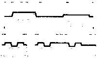
图3所示为沿图2的线III-III’,IV-IV’,V-V’,VI-VI’得到的水平电场施加型薄膜晶体管基板的截面图;Fig. 3 is shown along the line III-III ' of Fig. 2, IV-IV ', V-V ', the sectional view of the horizontal electric field application type thin film transistor substrate that VI-VI ' obtains;
图4示出了根据本发明另一实施例的水平电场施加型薄膜晶体管基板的一部分的平面图;4 shows a plan view of a part of a horizontal electric field applied thin film transistor substrate according to another embodiment of the present invention;
图5示出了使用图3所示的水平电场施加型薄膜晶体管基板的液晶显示板的数据焊盘区域的截面图;5 shows a cross-sectional view of the data pad area of the liquid crystal display panel using the horizontal electric field applied thin film transistor substrate shown in FIG. 3;
图6A和图6B分别示出了根据本发明实施例制造水平电场施加型薄膜晶体管基板的方法中第一掩模工序的平面图和截面图;6A and 6B respectively show a plan view and a cross-sectional view of a first mask process in a method for manufacturing a horizontal electric field applied thin film transistor substrate according to an embodiment of the present invention;
图7A至图7E示出了本发明的第一掩模工序的截面图;7A to 7E show cross-sectional views of the first masking process of the present invention;
图8A和图8B分别示出了根据本发明实施例制造水平电场施加型薄膜晶体管基板的方法中第二掩模工序的平面图和截面图;8A and 8B respectively show a plan view and a cross-sectional view of a second mask process in a method for manufacturing a horizontal electric field applied thin film transistor substrate according to an embodiment of the present invention;
图9A至图9F示出了解释第二掩模工序的截面图;9A to 9F show cross-sectional views explaining the second mask process;
图10A和图10B分别示出了根据本发明实施例制造水平电场施加型薄膜晶体管基板的方法中第三掩模工序的平面图和截面图;10A and 10B respectively show a plan view and a cross-sectional view of a third mask process in a method for manufacturing a horizontal electric field applied thin film transistor substrate according to an embodiment of the present invention;
图11A至图11E示出了第三掩模工序的截面图;11A to 11E show cross-sectional views of a third mask process;
图12示出了根据本发明另一实施例的水平电场施加型薄膜晶体管基板的一部分的平面图;以及12 shows a plan view of a part of a horizontal electric field application type thin film transistor substrate according to another embodiment of the present invention; and
图13为沿图12的线III-III’,IV-IV’,V-V’和VI-VI’得到的薄膜晶体管基板的截面图。13 is a cross-sectional view of the thin film transistor substrate taken along lines III-III', IV-IV', V-V' and VI-VI' of FIG. 12 .
具体实施方式Detailed ways
现在将对本发明的实施方式进行详细描述,所附附图示出了这些实施方式的实施例。Reference will now be made in detail to embodiments of the invention, examples of which are illustrated in the accompanying drawings.
图2示出了根据本发明实施例的水平电场施加型薄膜晶体管基板的结构的平面图,图3示出了沿图2的线III-III’,IV-IV’,V-V’,VI-VI’得到的薄膜晶体管基板的截面图。2 shows a plan view of the structure of a horizontal electric field application type thin film transistor substrate according to an embodiment of the present invention, and FIG. VI' Cross-sectional view of the obtained TFT substrate.
在图2和图3中,水平电场施加型薄膜晶体管基板包括以彼此相交、其间具有栅绝缘膜152的方式设置在下基板150上并限定像素区域的栅线102和数据线104,连接到栅线102和数据线104的薄膜晶体管TFT,和像素电极118。像素电极118和公共电极122在所述像素区域处形成水平电场。公共线120连接到公共电极122,存储电容器Cst设置在公共电极122和漏极112之间的重叠部分处。此外,薄膜晶体管基板包括连接到栅线102的栅焊盘124,连接到数据线104的数据焊盘132,和连接到公共线120的公共焊盘140。In FIGS. 2 and 3 , the horizontal electric field application type thin film transistor substrate includes
栅线102提供来自栅驱动器(未示出)的扫描信号;而数据线104提供来自数据驱动器(未示出)的视频信号。其间具有栅绝缘膜152的栅线102和数据线104彼此相交以限定像素区域。The
栅线102以具有至少双层栅金属层的多层结构形成在基板150上。例如,如图3所示,栅线102具有双层结构,其中构建有使用透明导电层的第一导电层101和由不透明金属形成的第二导电层103。数据线104以具有至少双层栅金属层的多层结构形成在栅绝缘膜152上。例如,如图3所示,数据线104具有双层结构,其中形成使用透明导电层的第三导电层111和由不透明金属形成的第四导电层113。第一和第三导电层101和111由例如IT0、T0、IZ0或ITZ0等形成。第二和第四导电层103和113由例如Cu、Mo、Al、Cu合金、Mo合金和Al合金等形成。The gate lines 102 are formed on the
薄膜晶体管TFT响应施加到栅线102的扫描信号,允许施加到数据线104的视频信号充入像素电极118并保持。为此,薄膜晶体管包括从栅线102延伸的栅极,连接到数据线104的源极110,与源极110相对并连接到像素电极118的漏极112,重叠栅线102的有源层114,其间具有栅绝缘膜152,以提供源极110和漏极112之间的沟道,和形成在有源层114上除了沟道部分以外的部分上的欧姆接触层116,以对源极110和漏极112提供欧姆接触。这里,源极110和漏极112具有双层结构,其中第三和第四导电层111和113与数据线104一起形成在栅绝缘膜152和半导体图案115上。The thin film transistor TFT allows a video signal applied to the
公共线120和公共电极122为每个像素提供驱动液晶的参考电压,即公共电压。The
为此,公共线120包括在显示区域处平行于栅线102设置的内部公共线120A,和在非显示区域处公共连接到内部公共线120A的外部公共线120B。公共线120具有双层结构,其中第一导电层和第二导电层101和103与上述栅线102一起形成在基板150上。For this, the
公共电极122设置在像素区域内并连接到内部公共线120A。更具体地,公共电极122包括重叠相邻于栅线102的漏极112的水平部分122A,和从水平部分122A延伸至像素区域中并连接到内部公共线120A的指状部分122B。公共电极122由公共线120的第一导电层即透明导电层形成。The
存储电容器Cst设置以便公共电极122的第一水平部分122A与漏极112重叠,其间具有栅绝缘膜152。这里,漏极1 12从它和薄膜晶体管TFT即栅线102之间的重叠部分延伸,以尽可能宽的方式与公共电极122的水平部分122A重叠。从而,存储电容器Cst的电容量通过公共电极122A和漏极112之间的宽重叠区域而增加,因此存储电容器Cst允许在像素电极118中充入的视频信号稳定地保持,直到充入下一个信号。The storage capacitor Cst is disposed so that the first
像素电极118以具有基本平行于公共电极122的指状部分122B的指状形状从漏极112延伸。像素电极118的边缘与内部公共线120A重叠。特别地,像素电极118由从漏极112延伸的第三导电层111即透明导电层形成。如果视频信号经由薄膜晶体管施加到像素电极118,那么在像素电极118和提供有公共电压的公共电极122的指状部分122B之间形成水平电场。通过这种水平电场在薄膜晶体管阵列基板和滤色片阵列基板之间沿水平方向排列的液晶分子由于介电各向异性而发生旋转。透过像素区域的光的透射率根据液晶分子的旋转程度而不同,由此实现灰度级。The
这里,当公共电极122和像素电极118形成水平电场时,公共电极122的指状部分122B和像素电极118的每侧(从边缘向内约1μm的区域)有助于孔径比,由此提高孔径比。Here, when the
此外,如图4所示,公共电极122的指状部分122B和像素电极118的指状部分可以形成之字形状。在公共电极122的指状部分122B中相邻于数据线104的边缘以基本平行于数据线104的方式或以之字形形成。同样,数据线104可以沿相邻公共电极122的指状部分122B以之字形形成。In addition, as shown in FIG. 4, the
栅线102经由栅焊盘124连接到栅驱动器(未示出)。栅焊盘124由从栅线102延伸的下栅焊盘电极126,和上栅焊盘电极130组成,所述上栅焊盘电极130经由贯穿栅绝缘膜152的第一接触孔128连接到下栅焊盘电极126。The
数据线104经由数据焊盘132连接到数据驱动器(未示出)。数据焊盘132由连接到数据链路135的下数据焊盘电极134,和经由贯穿栅绝缘膜152的第二接触孔136连接到下数据焊盘电极134的上数据焊盘电极138组成。The
公共线120经由公共焊盘140接收来自公共电压源(未示出)的参考电压。公共焊盘140由从外部公共线120B延伸的下公共焊盘电极142和上公共焊盘电极146组成,所述上公共焊盘电极146经由贯穿栅绝缘膜152的第三接触孔144连接到下公共焊盘电极142。The
在根据本发明实施例的薄膜晶体管基板中,数据焊盘132具有与栅焊盘124和公共焊盘140相同的结构。更具体地,下栅焊盘电极126,下公共焊盘电极142,下数据焊盘电极134和数据链路135具有双层结构,其中第一导电层和第二导电层101和103与上述栅线102一起形成在基板150上。同样,上栅焊盘电极130,上公共焊盘电极146和上数据焊盘电极138与数据线104一起形成在栅绝缘膜152上,并且由其中去除了第四导电层113的第三导电层111形成,该第三导电层为透明导电层。In the thin film transistor substrate according to an embodiment of the present invention, the
因此,在基板150上形成的数据链路135经由贯穿栅绝缘膜152的第四接触孔148连接到数据线104。数据链路135从下数据焊盘电极134延伸,从而具有第一和第二导电层101和103形成的结构。数据链路135的第二导电层103通过第四接触孔148暴露以便连接到数据线104的第三导电层111。在该情况下,数据线104的第三导电层111与上数据焊盘电极138为整体。数据线104由于不存在保护膜而暴露。为了防止数据线104的第四导电层113暴露在其外部并被氧化,如图5所示,第四接触孔148设置在由密封剂200密封的区域内。因此,位于在密封区域内的数据线104的第四导电层113被将在其上形成的下定向膜214保护。Accordingly, the data link 135 formed on the
参考图5,形成有下定向膜214的薄膜晶体管基板和涂敷有上定向膜212的滤色片基板2 10通过密封剂200彼此连接,通过密封剂200密封的两个基板之间的盒间隙充满液晶。在该情况下,液晶可以通过液晶滴注法或真空注入法形成,在液晶滴注法中,液晶层通过在至少一个基板上滴注液晶然后将它们连接而形成,在真空注入法中,连接两个基板然后注入液晶。上和下定向膜212和214由有机绝缘材料形成在两个基板的每个图像显示区域处。密封剂200以不与上和下定向膜212和214接触的方式形成,以便增强粘合力。从而,设置在薄膜晶体管基板上的数据线104,源极110,漏极112和像素电极118设置在由密封剂200密封的区域处,因此可以得到在其上形成的下定向膜214以及填充在密封区域中的液晶的充分保护。Referring to FIG. 5, a thin film transistor substrate formed with a
如上所述根据本发明第一实施例的不具有保护膜的水平电场施加型薄膜晶体管基板通过下述三次掩模工序形成。The horizontal electric field application type thin film transistor substrate having no protective film according to the first embodiment of the present invention as described above is formed through the following three masking processes.
图6A和图6B分别为根据本发明实施例制造水平电场施加型薄膜晶体管基板的方法中第一掩模工序的平面图和截面图,图7A至图7E为更具体说明第一掩模工序的截面图。6A and 6B are respectively a plan view and a cross-sectional view of the first mask process in the method for manufacturing a horizontal electric field applied thin film transistor substrate according to an embodiment of the present invention, and FIGS. 7A to 7E are cross-sections illustrating the first mask process in more detail. picture.
通过第一掩模工序在下基板150上形成第一掩模图案组,第一掩模图案组包括栅线102,下栅焊盘电极126,公共线120,公共电极122,下公共焊盘电极142,数据链路135和下数据焊盘电极134。这里,除公共电极122以外的第一掩模图案组具有由至少两层导电层形成的多层结构。为了方便,将解释具有第一和第二导电层101和103的双层结构。公共电极122具有由为透明导电层的第一导电层101构成的单层结构。具有多层结构和单层结构的第一掩模图案组通过利用例如衍射曝光掩模或半色调掩模等的单轮掩模工序形成。在下文中,将描述半色调掩模用作第一掩模的情况。A first mask pattern group is formed on the
在图7A中,第一和第二导电层101和103通过沉积技术如溅射等设置在下基板150上。第一导电层101由透明导电材料如ITO、TO、IZO或ITZO等形成。第二导电层103使用由金属材料形成的单层或至少双层的多层结构,金属材料例如Mo、Ti、Cu、AlNd、Al、Cr、Mo合金、Cu合金或Al合金等,多层例如Al/Cr、Al/Mo、Al(Nd)/Al、Al(Nd)/Cr、Mo/Al(Nd)/Mo、Cu/Mo、Ti/Al(Nd)/Ti、Mo/Al、Mo/Ti/Al(Nd)、Cu合金/Mo、Cu合金/Al、Cu合金/Mo合金、Cu合金/Al合金、Al/Mo合金、Mo合金/Al、Al合金/Mo合金、Mo合金/Al合金、Mo/Al合金等。In FIG. 7A, first and second
参考图7B,通过利用半色调掩模的光刻形成具有台阶敷层的第一光刻胶图案162。半色调掩模由遮蔽紫外线的遮蔽部分,利用相移材料部分透射紫外线的半色调透射部分,以及完全透射紫外线的完全透射部分构成。第一光刻胶图案162包括不同厚度的第一光刻胶图案162A和162B和通过利用半色调掩模的光刻形成开口部分。在该情况下,相对厚的第一光刻胶图案162A设置在与半色调掩模的遮蔽部分重叠的第一光刻胶的遮蔽区域P1处;第一光刻胶图案162B比第一光刻胶图案162A薄并且设置在重叠半色调透射部分的半色调曝光区域P2处;以及开口部分设置在与完全透射部分重叠的完全曝光区域P3处。Referring to FIG. 7B, a first photoresist pattern 162 having a stepped coating is formed by photolithography using a half tone mask. A halftone mask consists of a shielding portion that blocks ultraviolet rays, a halftone transmissive portion that partially transmits ultraviolet rays using a phase-shift material, and a fully transmissive portion that completely transmits ultraviolet rays. The first photoresist pattern 162 includes first photoresist patterns 162A and 162B of different thicknesses and an opening portion is formed by photolithography using a half tone mask. In this case, a relatively thick first photoresist pattern 162A is disposed at the masked region P1 of the first photoresist overlapping with the masked portion of the halftone mask; the first photoresist pattern 162B is thicker than the first photoresist The glue pattern 162A is thin and provided at the halftone exposure area P2 overlapping the halftone transmission part; and the opening part is provided at the full exposure area P3 overlapping the full transmission part.
参考图7C,通过利用第一光刻胶图案162作为掩模的刻蚀工序刻蚀第一和第二导电层101和103的暴露部分,由此提供包括双层结构的栅线102,下栅焊盘电极126,公共线120,公共电极122,下公共焊盘电极142,数据链路135和下数据焊盘电极134的第一掩模图案组。Referring to FIG. 7C, the exposed portions of the first and second
在图7D中,通过利用氧(O2)等离子体的灰化工序第一光刻胶图案162A的厚度变薄,同时去除第一光刻胶图案162B。此外,通过利用已灰化第一光刻胶图案162A作为掩模的刻蚀工序去除公共电极122上的第二导电层103。在该情况下,构图案后的第二导电层103的每侧沿已灰化第一光刻胶图案162A再次进行刻蚀,由此允许第一掩模图案组的第一和第二导电层101和103具有以基本为矩形或梯形的恒定的台阶敷层。因此,当第一和第二导电层101和103的侧面具有大的倾斜度时,可以防止在其上产生的栅绝缘膜152的台阶敷层损坏。In FIG. 7D, the thickness of the first photoresist pattern 162A is thinned through an ashing process using oxygen (O2 ) plasma, and the first photoresist pattern 162B is simultaneously removed. In addition, the second
参考图7E,通过剥离工序去除在图7D中剩余在第一掩模图案组上的第一光刻胶图案162A。Referring to FIG. 7E, the first photoresist pattern 162A remaining on the first mask pattern group in FIG. 7D is removed through a lift-off process.
图8A和图8B分别为解释根据本发明实施例制造水平电场施加型薄膜晶体管基板的方法中第二掩模工序的平面图和截面图,图9A至图9F为更具体解释第二掩模工序的截面图。8A and 8B are respectively a plan view and a cross-sectional view for explaining the second mask process in the method for manufacturing a horizontal electric field application type thin film transistor substrate according to an embodiment of the present invention, and FIGS. 9A to 9F are for explaining the second mask process in more detail. Sectional view.
通过第二掩模工序在设有第一掩模图案组的下基板150上形成包括第一至第四接触孔128、136、144和148的栅绝缘膜152以及半导体图案115。半导体图案115和栅绝缘膜152的接触孔128、136、144和148通过利用衍射曝光掩模或半色调掩模的单轮掩模工序限定。在下文中,将描述半色调掩模用作第二掩模的情况。The
在图9A中,通过沉积技术如PECVD等在形成有第一掩模图案的下基板150上顺序设置栅绝缘膜152,非晶硅层105和掺杂有n+或p+杂质的非晶硅层107。这里,栅绝缘膜152由无机绝缘材料如氧化硅(SiOx)或氮化硅(SiNx)形成。In FIG. 9A, a
在图9B中,通过利用半色调掩模的光刻形成具有台阶敷层的第二光刻胶图案168。半色调掩模由遮蔽紫外线的遮蔽部分,利用相移材料部分透射紫外线的半色调透射部分,以及完全透射紫外线的完全透射部分构成。第二光刻胶图案168包括不同厚度的第二光刻胶图案168A和168B,以及通过利用半色调掩模的光刻形成开口部分。在该情况下,相对厚的第二光刻胶图案168A设置在第二光刻胶与半色调掩模的遮蔽部分重叠的遮蔽区域P1处;第二光刻胶图案162B比第二光刻胶图案162A薄并且设置与半色调透射部分重叠的半色调曝光区域P2处;以及开口部分设置在与完全透射部分重叠的完全曝光区域P3处。In FIG. 9B, a
在图9C中,通过利用第二光刻胶图案168作为掩模的刻蚀工序形成贯穿从掺杂有n+或p+杂质的非晶硅层107到栅绝缘膜152的第一至第四接触孔128、136、144和148。第一接触孔128暴露下栅焊盘电极126;第二接触孔136暴露下数据焊盘电极134;第三接触孔144暴露下公共焊盘电极142;以及第四接触孔148暴露数据链路135。In FIG. 9C, the first to fourth layers penetrating from the
参考图9D,通过利用氧(O2)等离子体的灰化工序第二光刻胶图案168A的厚度变薄,同时去除第二光刻胶图案168B。Referring to FIG. 9D , the thickness of the
参考图9E,通过利用已灰化第二光刻胶图案168A作为掩模的刻蚀工序形成构图掺杂有n+或p+杂质的非晶硅层107和非晶硅层105,由此提供包括有源层114和欧姆接触层116的半导体图案115。Referring to FIG. 9E, the
在图9F中,通过剥离工序去除在图9E中剩余在半导体图案115上的第二光刻胶图案168A。In FIG. 9F, the
图10A和图10B分别为解释根据本发明实施例制造水平电场施加型薄膜晶体管基板的方法中第三掩模工序的平面图和截面图,图11A至图11E为更具体解释第三掩模工序的截面图。10A and 10B are respectively a plan view and a cross-sectional view for explaining the third mask process in the method for manufacturing a horizontal electric field application type thin film transistor substrate according to an embodiment of the present invention, and FIGS. 11A to 11E are for explaining the third mask process in more detail. Sectional view.
通过第三掩模工序在设有半导体图案115的栅绝缘膜152上形成第三掩模图案组,其包括数据线104,源极110,漏极112,像素电极118,上栅焊盘电极130,上数据焊盘电极138和上公共焊盘电极146。这里,包括数据线104、源极110和漏极112的第三掩模图案组A具有由至少两层导电层形成的多层结构。为了方便,将描述具有第三和第四导电层111和113的双层结构。包括像素电极118、上栅焊盘电极130、上数据焊盘电极138和上公共焊盘电极146的第三掩模图案组B具有由第三掩模图案组A的第三导电层111形成的单层结构。通过利用衍射曝光掩模或半色调掩模的第三掩模工序形成包括具有双层结构的第三掩模图案组A和具有单层结构的第三掩模图案组B的第三掩模图案组。在下文中,将描述半色调掩模作为第三掩模的情况。Through the third mask process, a third mask pattern group is formed on the
在图11A中,通过沉积技术如溅射在形成有半导体图案115的栅绝缘膜152上顺序形成第三和第四导电层111和113。第三导电层111由透明导电材料如ITO、TO、IZO或ITZO等形成,或具有强耐腐蚀性和高强度的不透明金属如Ti或W等形成。第四导电层113使用由金属材料形成的单层或具有至少双层的多层结构,金属材料例如Mo、Ti、Cu、AlNd、Al、Cr、Mo合金、Cu合金或Al合金,多层例如Al/Cr、Al/Mo、Al(Nd)/Al、Al(Nd)/Cr、Mo/Al(Nd)/Mo、Cu/Mo、Ti/Al(Nd)/Ti、Mo/Al、Mo/Ti/Al(Nd)、Cu合金/Mo、Cu合金/Al、Cu合金/Mo合金、Cu合金/Al合金、Al/Mo合金、Mo合金/Al、Al合金/Mo合金、Mo合金/Al合金、Mo/Al合金等。In FIG. 11A, third and fourth
在图11B中,通过利用半色调掩模的光刻形成具有台阶敷层的第三光刻胶图案182。半色调掩模由遮蔽紫外线的遮蔽部分,利用相移材料部分透射紫外线的半色调透射部分,以及完全透射紫外线的完全透射部分构成。第三光刻胶图案182包括不同厚度的第三光刻胶图案182A和182B,以及通过利用半色调掩模的光刻形成开口部分。在该情况下,相对厚的第三光刻胶图案182A设置在第三光刻胶与半色调掩模的遮蔽部分重叠的遮蔽区域P1处;第三光刻胶图案182B比第三光刻胶图案182A薄并且设置在与半色调透射部分重叠的半色调曝光区域P2处;以及开口部分设置在与完全透射部分重叠的完全曝光区域P3处。In FIG. 11B, a
参考图11C,通过利用第三光刻胶图案182作为掩模的湿刻工序形成构图第三和第四导电层111和113,由此提供双层结构的数据线104,源极110,漏极112,像素电极118,上栅焊盘电极130,上数据焊盘电极138和上公共焊盘电极146。数据线104与数据链路135重叠并经由第四接触孔148连接到数据链路135。在该情况下,由于第四导电层113被刻蚀,然后第三导电层111通过不同的刻蚀剂进行刻蚀,因此位于比上面的第四导电层113更低部分处的第三导电层111被过刻蚀,以产生底切区域。此外,通过利用源极110和漏极112作为掩模的刻蚀工序例如干刻工序去除在源极110和漏极112之间的欧姆接触层116,由此暴露有源层114。Referring to FIG. 11C, the third and fourth
参考图11D,通过灰化工序第三光刻胶图案182A的厚度变薄,同时去除第三光刻胶图案182B。这种灰化工序可以在与断开欧姆接触层116的干刻工序相同的室中进行。第三光刻胶图案182B的去除暴露像素电极118的第四导电层113,上栅焊盘电极130的第四导电层113,上数据焊盘电极138的第四导电层113和上公共焊盘电极146的第四导电层113。此外,已灰化第三光刻胶图案182A的边缘位于在构图后的第四导电层113边缘的内侧。Referring to FIG. 11D , the thickness of the
参考图11E,通过利用已灰化第三光刻胶图案182A作为掩模的刻蚀工序刻蚀像素电极118的第四导电层113,上栅焊盘电极130的第四导电层113,上数据焊盘电极138的第四导电层113和上公共焊盘电极146的第四导电层113,由此提供具有第三导电层111的单层结构的像素电极118,上栅焊盘电极130,上数据焊盘电极138和上公共焊盘电极146。在该情况下,通过第三光刻胶图案182A的边缘暴露的第四导电层113的每侧再次进行刻蚀。从而,数据线104、源极110和漏极112的第三和第四导电层111和113具有恒定的台阶敷层,其具有基本上矩形或梯形的形状。此外,第三光刻胶图案182A通过剥离工序去除。Referring to FIG. 11E, the fourth
在第三掩模工序中的第三和第四导电层111和113的刻蚀工序可以通过湿刻或干刻进行。但是,优选湿刻。The etching process of the third and fourth
结果,根据本发明实施例的水平电场施加型薄膜晶体管基板具有由于不存在保护膜而暴露结构的数据线104、源极110和像素电极118。然而,它们所有都定位在由密封剂密封的区域处,因此它们可以得到其上涂敷的下定向膜以及充填在密封区域中的液晶的充分保护。As a result, the horizontal electric field application type thin film transistor substrate according to an embodiment of the present invention has the
图12示出了根据本发明另一实施例的水平电场施加型薄膜晶体管基板的一部分的平面图,和图13为沿图12的线III-III’,IV-IV’,V-V’和VI-VI’得到的薄膜晶体管基板的截面图。FIG. 12 shows a plan view of a part of a horizontal electric field application type thin film transistor substrate according to another embodiment of the present invention, and FIG. 13 is a plan view along lines III-III', IV-IV', V-V' and VI of FIG. -VI' Cross-sectional view of the thin film transistor substrate obtained.
除了栅焊盘224、数据焊盘232和公共焊盘240通过第一掩模工序形成从而具有第一掩模图案组结构之外,图12和图13中示出的薄膜晶体管基板具有与图2和图3中示出的薄膜晶体管基板相同的元件。因此,相同元件的说明将省略。The thin film transistor substrate shown in FIGS. 12 and 13 has the same structure as that of FIG. The same elements as the thin film transistor substrate shown in FIG. 3 . Therefore, descriptions of the same elements will be omitted.
参考图12和图13,下栅焊盘电极230、下数据焊盘电极238和下公共焊盘电极246由第一掩模图案组的第一导电层101形成。下栅焊盘电极230、下数据焊盘电极238和下公共焊盘电极246分别通过第一至第三接触孔228、236和244暴露。上栅焊盘电极226、上数据焊盘电极234和上公共焊盘电极242由第一掩模图案组的第二导电层103形成。上焊盘电极226、234和242以不与接触孔228、236和244重叠的方式留在下焊盘电极230、238和246上,因此得到栅绝缘膜152的保护。例如,上焊盘电极226、234和242沿下焊盘电极230、238和246的边缘形成,因此得到栅绝缘膜152的保护。Referring to FIGS. 12 and 13 , the lower
贯穿上焊盘电极226、234和242的下焊盘电极230、238和246的暴露结构通过以暴露第一导电层101的方式仅刻蚀掉第二导电层103形成,该刻蚀通过在第一掩模工序中应用半色调曝光区域P2来进行,如上参考图6A至图7E所述。The exposed structure of the
如上所述,在根据本发明的水平电场施加型薄膜晶体管基板及其制造方法中,借助于第一半色调(或衍射曝光)掩模,形成单层结构的公共电极,以及多层结构的其他第一掩模图案组。As described above, in the horizontal electric field application type thin film transistor substrate and its manufacturing method according to the present invention, by means of the first half-tone (or diffractive exposure) mask, the common electrode of the single-layer structure, and other electrodes of the multi-layer structure are formed. A first set of mask patterns.
此外,在根据本发明的水平电场施加型薄膜晶体管基板及其制造方法中,通过利用第二半色调(或衍射曝光)掩模形成半导体图案和接触孔。Furthermore, in the horizontal electric field application type thin film transistor substrate and the manufacturing method thereof according to the present invention, the semiconductor pattern and the contact hole are formed by using a second half tone (or diffractive exposure) mask.
此外,在根据本发明的水平电场施加型薄膜晶体管基板及其制造方法中,借助于第三半色调(或衍射曝光)掩模,形成单层结构的像素电极和上焊盘电极,以及多层结构的其他第三掩模图案组,而没有任何保护膜。In addition, in the horizontal electric field application type thin film transistor substrate and its manufacturing method according to the present invention, by means of a third halftone (or diffractive exposure) mask, a pixel electrode and an upper pad electrode of a single-layer structure are formed, and a multilayer structure of the other third mask pattern set without any protective film.
因此,整个工序可以通过三次掩模而简化,因此减少材料成本和设备投资成本,以及提高生产率等成为可能。Therefore, the entire process can be simplified by masking three times, so it is possible to reduce material costs and equipment investment costs, and increase productivity.
此外,根据本发明的水平电场施加型薄膜晶体管基板应用到其中的液晶板允许由于不存在保护膜而暴露的数据线、源极、漏极和像素电极得到在其上形成的下定向膜或填充在由密封剂密封的区域中的液晶的充分保护。同样,薄膜晶体管基板的焊盘具有相同结构,连接到数据焊盘的数据链路经由接触孔连接到密封剂密封的区域中的数据线。从而,防止由于保护膜的缺少引起的照明问题等成为可能。In addition, the liquid crystal panel to which the horizontal electric field application type thin film transistor substrate according to the present invention is applied allows data lines, source electrodes, drain electrodes, and pixel electrodes exposed due to the absence of a protective film to be formed thereon with a lower alignment film or filling Adequate protection of liquid crystals in areas sealed by sealant. Also, the pads of the thin film transistor substrate have the same structure, and the data link connected to the data pad is connected to the data line in the area sealed by the encapsulant via the contact hole. Thereby, it becomes possible to prevent lighting problems and the like due to the absence of the protective film.
此外,根据本发明,公共电极和像素电极由透明导电层形成,由此有助于孔径比,因此提高孔径比成为可能。Furthermore, according to the present invention, the common electrode and the pixel electrode are formed of a transparent conductive layer, thereby contributing to the aperture ratio, and thus it becomes possible to increase the aperture ratio.
本领域的技术人员应当理解在不脱离本发明的精神或范围的情况下本发明有多种变形和变化。因此,本发明覆盖所有落入所附权利要求和其等同物限定范围内的这些变形和变化。Those skilled in the art will understand that there are many modifications and changes in the present invention without departing from the spirit or scope of the invention. Accordingly, the present invention covers all such modifications and changes as come within the scope of the appended claims and their equivalents.
Claims (45)
Applications Claiming Priority (2)
| Application Number | Priority Date | Filing Date | Title |
|---|---|---|---|
| KR1020040112578AKR101085132B1 (en) | 2004-12-24 | 2004-12-24 | Horizontal field thin film transistor substrate and its manufacturing method |
| KR1020040112578 | 2004-12-24 |
Publications (2)
| Publication Number | Publication Date |
|---|---|
| CN1794076Atrue CN1794076A (en) | 2006-06-28 |
| CN100397224C CN100397224C (en) | 2008-06-25 |
Family
ID=36611023
Family Applications (1)
| Application Number | Title | Priority Date | Filing Date |
|---|---|---|---|
| CNB2005101322107AExpired - Fee RelatedCN100397224C (en) | 2004-12-24 | 2005-12-22 | Horizontal electric field applied thin film transistor substrate and manufacturing method thereof |
Country Status (4)
| Country | Link |
|---|---|
| US (2) | US7859639B2 (en) |
| JP (1) | JP4612539B2 (en) |
| KR (1) | KR101085132B1 (en) |
| CN (1) | CN100397224C (en) |
Cited By (15)
| Publication number | Priority date | Publication date | Assignee | Title |
|---|---|---|---|---|
| CN101349844B (en)* | 2007-07-20 | 2010-11-10 | 乐金显示有限公司 | Array substrate for liquid crystal display device and method of fabricating the same |
| US7916229B2 (en) | 2008-05-16 | 2011-03-29 | Lg Display Co., Ltd. | Liquid crystal display device and method for fabricating the same |
| CN102683277A (en)* | 2012-05-08 | 2012-09-19 | 深圳市华星光电技术有限公司 | Thin film transistor array substrate and making method thereof |
| CN103022056A (en)* | 2012-12-28 | 2013-04-03 | 北京京东方光电科技有限公司 | Array substrate, manufacturing method of array substrate, and display device |
| CN103022055A (en)* | 2012-12-28 | 2013-04-03 | 北京京东方光电科技有限公司 | Array substrate, manufacturing method of array substrate, and display device |
| CN103066017A (en)* | 2012-12-28 | 2013-04-24 | 北京京东方光电科技有限公司 | Preparing method of array substrate |
| CN103163702A (en)* | 2011-12-08 | 2013-06-19 | 乐金显示有限公司 | Narrow bezel-type liquid crystal display device |
| WO2013116994A1 (en)* | 2012-02-07 | 2013-08-15 | 深圳市华星光电技术有限公司 | Thin-film transistor array substrate and manufacturing method therefor |
| WO2014015453A1 (en)* | 2012-07-25 | 2014-01-30 | 京东方科技集团股份有限公司 | Thin film transistor, array substrate and manufacturing method thereof, and display device |
| CN105225929A (en)* | 2015-09-23 | 2016-01-06 | 京东方科技集团股份有限公司 | A kind of method of film pattern |
| CN106575063A (en)* | 2014-08-07 | 2017-04-19 | 夏普株式会社 | Active matrix substrate, liquid crystal panel and method for producing active matrix substrate |
| CN109597249A (en)* | 2017-10-03 | 2019-04-09 | 夏普株式会社 | Display panel |
| CN113589605A (en)* | 2021-07-29 | 2021-11-02 | 武汉京东方光电科技有限公司 | Array substrate, preparation method thereof and display panel |
| WO2022199019A1 (en)* | 2021-03-22 | 2022-09-29 | 京东方科技集团股份有限公司 | Array substrate and manufacturing method therefor, display panel, and display device |
| CN117651900A (en)* | 2022-03-21 | 2024-03-05 | 京东方科技集团股份有限公司 | Display substrate, preparation method thereof and display device |
Families Citing this family (34)
| Publication number | Priority date | Publication date | Assignee | Title |
|---|---|---|---|---|
| KR101096718B1 (en)* | 2004-12-24 | 2011-12-22 | 엘지디스플레이 주식회사 | Fabricating method of thin film transistor substrate of horizontal electric field |
| KR101107251B1 (en)* | 2004-12-31 | 2012-01-19 | 엘지디스플레이 주식회사 | Poly thin film transistor substrate and manufacturing method thereof |
| US7952099B2 (en)* | 2006-04-21 | 2011-05-31 | Beijing Boe Optoelectronics Technology Co., Ltd. | Thin film transistor liquid crystal display array substrate |
| KR100978263B1 (en)* | 2006-05-12 | 2010-08-26 | 엘지디스플레이 주식회사 | LCD and its manufacturing method |
| KR101244898B1 (en)* | 2006-06-28 | 2013-03-19 | 삼성디스플레이 주식회사 | Organic Thin Film Transistor Substrate And Fabricating Method Thereof |
| KR101337178B1 (en)* | 2006-06-29 | 2013-12-05 | 엘지디스플레이 주식회사 | Array substrate for LCD and the fabrication method thereof |
| KR101197059B1 (en) | 2006-07-11 | 2012-11-06 | 삼성디스플레이 주식회사 | Thin film transistor array panel and method for manufacturing the same |
| KR101293573B1 (en) | 2006-10-02 | 2013-08-06 | 삼성디스플레이 주식회사 | Thin film transistor panel and manufacturing method thereof |
| KR101383703B1 (en)* | 2007-10-04 | 2014-04-10 | 삼성디스플레이 주식회사 | Thin film transistor array panel and manufacturung method thereof |
| KR101441545B1 (en)* | 2008-01-02 | 2014-09-17 | 삼성디스플레이 주식회사 | Display substrate and manufacturing method thereof |
| CN101807586B (en)* | 2009-02-13 | 2013-07-31 | 北京京东方光电科技有限公司 | TFT-LCD (Thin Film Transistor Liquid Crystal Display) array substrate and manufacturing method thereof |
| JP5239924B2 (en) | 2009-02-16 | 2013-07-17 | Nltテクノロジー株式会社 | Liquid crystal display device and electronic apparatus using the same |
| CN101887897B (en)* | 2009-05-13 | 2013-02-13 | 北京京东方光电科技有限公司 | TFT-LCD (Thin Film Transistor Liquid Crystal Display) array base plate and manufacturing method thereof |
| CN101957526B (en) | 2009-07-13 | 2013-04-17 | 北京京东方光电科技有限公司 | TFT-LCD (Thin Film Transistor-Liquid Crystal Display) array substrate and manufacturing method thereof |
| CN102023433B (en)* | 2009-09-18 | 2012-02-29 | 北京京东方光电科技有限公司 | TFT-LCD array substrate and manufacturing method thereof |
| JP5139503B2 (en)* | 2010-11-18 | 2013-02-06 | 株式会社ジャパンディスプレイイースト | Liquid crystal display device and manufacturing method thereof |
| JP2012118199A (en)* | 2010-11-30 | 2012-06-21 | Panasonic Liquid Crystal Display Co Ltd | Liquid crystal panel, liquid crystal display device, and manufacturing method thereof |
| KR101258903B1 (en)* | 2012-02-24 | 2013-04-29 | 엘지디스플레이 주식회사 | Liquid crystal display device and the method of fabricating thereof |
| US9158133B1 (en) | 2012-07-26 | 2015-10-13 | Google Inc. | Contact lens employing optical signals for power and/or communication |
| CN103293803B (en)* | 2012-12-26 | 2016-08-03 | 成都天马微电子有限公司 | Array base palte and manufacture method thereof for FFS mode liquid crystal display |
| KR102092544B1 (en)* | 2012-12-29 | 2020-04-16 | 엘지디스플레이 주식회사 | Array substrate for liquid crystal display device and method of fabricating the same |
| TWI548924B (en)* | 2013-06-04 | 2016-09-11 | 群創光電股份有限公司 | Display panel and display device |
| JP2015012048A (en)* | 2013-06-27 | 2015-01-19 | 三菱電機株式会社 | Active matrix substrate and manufacturing method thereof |
| KR102062913B1 (en)* | 2013-09-30 | 2020-03-02 | 엘지디스플레이 주식회사 | Thin film transistor array substrate and method of manufacturing the same |
| JP6223809B2 (en)* | 2013-12-18 | 2017-11-01 | 株式会社ジャパンディスプレイ | Display device |
| TWI548909B (en)* | 2014-02-17 | 2016-09-11 | 晶典有限公司 | Wafer level assembly structure of display module for liquid crystal on silicon and method for manufacturing the same |
| CN104020593A (en)* | 2014-05-30 | 2014-09-03 | 深圳市华星光电技术有限公司 | Array substrate, manufacturing method and liquid crystal display panel |
| CN104460132B (en)* | 2014-12-16 | 2017-11-07 | 京东方科技集团股份有限公司 | Liquid crystal grating and preparation method thereof, display device |
| KR102373687B1 (en)* | 2015-05-11 | 2022-03-17 | 삼성디스플레이 주식회사 | Display device and method for fabricating the same |
| CN107092111B (en)* | 2016-02-17 | 2021-06-11 | 群创光电股份有限公司 | Active element array substrate and display panel |
| CN105895639A (en)* | 2016-06-29 | 2016-08-24 | 京东方科技集团股份有限公司 | Array substrate, fabrication method thereof and display device |
| KR102766820B1 (en)* | 2016-08-29 | 2025-02-11 | 엘지디스플레이 주식회사 | Display device having narrow bezel |
| JP2018132589A (en)* | 2017-02-14 | 2018-08-23 | 株式会社ジャパンディスプレイ | Display device |
| WO2022032590A1 (en)* | 2020-08-13 | 2022-02-17 | 重庆康佳光电技术研究院有限公司 | Display panel and electronic device |
Family Cites Families (32)
| Publication number | Priority date | Publication date | Assignee | Title |
|---|---|---|---|---|
| US5162933A (en)* | 1990-05-16 | 1992-11-10 | Nippon Telegraph And Telephone Corporation | Active matrix structure for liquid crystal display elements wherein each of the gate/data lines includes at least a molybdenum-base alloy layer containing 0.5 to 10 wt. % of chromium |
| US5163922A (en)* | 1991-04-29 | 1992-11-17 | Charles E. McElveen, Jr. | Dual-valved connector for intravenous systems |
| KR940004322B1 (en)* | 1991-09-05 | 1994-05-19 | 삼성전자 주식회사 | Liquid crystal display devices |
| US5317433A (en)* | 1991-12-02 | 1994-05-31 | Canon Kabushiki Kaisha | Image display device with a transistor on one side of insulating layer and liquid crystal on the other side |
| DE4339721C1 (en)* | 1993-11-22 | 1995-02-02 | Lueder Ernst | Method for producing a matrix of thin-film transistors |
| TW321731B (en)* | 1994-07-27 | 1997-12-01 | Hitachi Ltd | |
| JP3866783B2 (en)* | 1995-07-25 | 2007-01-10 | 株式会社 日立ディスプレイズ | Liquid crystal display |
| KR0156202B1 (en)* | 1995-08-22 | 1998-11-16 | 구자홍 | LCD and its manufacturing method |
| US5835177A (en)* | 1995-10-05 | 1998-11-10 | Kabushiki Kaisha Toshiba | Array substrate with bus lines takeout/terminal sections having multiple conductive layers |
| JPH09113931A (en)* | 1995-10-16 | 1997-05-02 | Sharp Corp | Liquid crystal display |
| JP3625598B2 (en)* | 1995-12-30 | 2005-03-02 | 三星電子株式会社 | Manufacturing method of liquid crystal display device |
| KR100251512B1 (en)* | 1997-07-12 | 2000-04-15 | 구본준 | Transverse electric field liquid crystal display device |
| KR100272537B1 (en) | 1997-10-09 | 2000-11-15 | 구본준 | An in plane switching mode liquid crystal display device |
| JPH11264993A (en) | 1998-03-18 | 1999-09-28 | Toshiba Corp | Liquid crystal display device and method of manufacturing liquid crystal display device |
| TW413949B (en)* | 1998-12-12 | 2000-12-01 | Samsung Electronics Co Ltd | Thin film transistor array panels for liquid crystal displays and methods of manufacturing the same |
| KR100318534B1 (en) | 1999-01-15 | 2001-12-22 | 윤종용 | Liquid crystal display and manufacturing method thereof |
| CN1195243C (en)* | 1999-09-30 | 2005-03-30 | 三星电子株式会社 | Film transistor array panel for liquid crystal display and its producing method |
| KR100325079B1 (en)* | 1999-12-22 | 2002-03-02 | 주식회사 현대 디스플레이 테크놀로지 | Method of manufacturing lcd having high aperture ratio and high transmittance |
| KR100322970B1 (en)* | 1999-12-24 | 2002-02-02 | 주식회사 현대 디스플레이 테크놀로지 | Method for manufacturing fringe field switching mode lcd |
| JP5408829B2 (en) | 1999-12-28 | 2014-02-05 | ゲットナー・ファンデーション・エルエルシー | Method for manufacturing active matrix substrate |
| JP2001255543A (en)* | 2000-03-10 | 2001-09-21 | Hitachi Ltd | Liquid crystal display |
| TW498178B (en)* | 2000-05-02 | 2002-08-11 | Hannstar Display Corp | Manufacturing method and structure for in-plane switching mode liquid crystal display unit |
| JP4342711B2 (en) | 2000-09-20 | 2009-10-14 | 株式会社日立製作所 | Manufacturing method of liquid crystal display device |
| JP2002202527A (en)* | 2000-12-28 | 2002-07-19 | Nec Corp | Active matrix type liquid crystal display device |
| GB0102167D0 (en) | 2001-01-27 | 2001-03-14 | Koninl Philips Electronics Nv | Pixellated devices such as active matrix liquid crystal displys and methods of manufacturing such |
| KR100685946B1 (en) | 2001-03-02 | 2007-02-23 | 엘지.필립스 엘시디 주식회사 | Liquid crystal display panel and manufacturing method thereof |
| KR100803177B1 (en)* | 2001-05-14 | 2008-02-14 | 삼성전자주식회사 | Thin film transistor for liquid crystal display device and manufacturing method thereof |
| KR100473588B1 (en)* | 2001-12-28 | 2005-03-08 | 엘지.필립스 엘시디 주식회사 | array panel for liquid crystal display devices |
| KR100904269B1 (en)* | 2002-12-31 | 2009-06-25 | 엘지디스플레이 주식회사 | LCD Display |
| KR100538327B1 (en) | 2003-04-03 | 2005-12-22 | 엘지.필립스 엘시디 주식회사 | Thin film transistor array substrate of horizontal electronic field applying type and fabricating method thereof |
| JP2004302466A (en)* | 2003-03-29 | 2004-10-28 | Lg Philips Lcd Co Ltd | Horizontal electric field application type liquid crystal display device and manufacturing method thereof |
| KR100470208B1 (en)* | 2003-04-03 | 2005-02-04 | 엘지.필립스 엘시디 주식회사 | Liquid crystal display apparatus of horizontal electronic field applying type and fabricating method thereof |
- 2004
- 2004-12-24KRKR1020040112578Apatent/KR101085132B1/ennot_activeExpired - Fee Related
- 2005
- 2005-12-20USUS11/311,553patent/US7859639B2/ennot_activeExpired - Fee Related
- 2005-12-22CNCNB2005101322107Apatent/CN100397224C/ennot_activeExpired - Fee Related
- 2005-12-22JPJP2005369463Apatent/JP4612539B2/ennot_activeExpired - Fee Related
- 2010
- 2010-11-22USUS12/951,907patent/US8111363B2/enactiveActive
Cited By (25)
| Publication number | Priority date | Publication date | Assignee | Title |
|---|---|---|---|---|
| US8045078B2 (en) | 2007-07-20 | 2011-10-25 | Lg Display Co., Ltd. | Array substrate for liquid crystal display device and method of fabricating the same |
| CN101349844B (en)* | 2007-07-20 | 2010-11-10 | 乐金显示有限公司 | Array substrate for liquid crystal display device and method of fabricating the same |
| US7916229B2 (en) | 2008-05-16 | 2011-03-29 | Lg Display Co., Ltd. | Liquid crystal display device and method for fabricating the same |
| US9618817B2 (en) | 2011-12-08 | 2017-04-11 | Lg Display Co., Ltd. | Array substrate and narrow bezel-type liquid crystal display device including the same |
| CN103163702A (en)* | 2011-12-08 | 2013-06-19 | 乐金显示有限公司 | Narrow bezel-type liquid crystal display device |
| WO2013116994A1 (en)* | 2012-02-07 | 2013-08-15 | 深圳市华星光电技术有限公司 | Thin-film transistor array substrate and manufacturing method therefor |
| CN102683277A (en)* | 2012-05-08 | 2012-09-19 | 深圳市华星光电技术有限公司 | Thin film transistor array substrate and making method thereof |
| WO2013166668A1 (en)* | 2012-05-08 | 2013-11-14 | 深圳市华星光电技术有限公司 | Thin film transistor array substrate and manufacturing method thereof |
| WO2014015453A1 (en)* | 2012-07-25 | 2014-01-30 | 京东方科技集团股份有限公司 | Thin film transistor, array substrate and manufacturing method thereof, and display device |
| US9209308B2 (en) | 2012-07-25 | 2015-12-08 | Boe Technology Group Co., Ltd. | Thin film transistor, array substrate and method for manufacturing the same, display device |
| CN103066017A (en)* | 2012-12-28 | 2013-04-24 | 北京京东方光电科技有限公司 | Preparing method of array substrate |
| CN103022056B (en)* | 2012-12-28 | 2015-04-29 | 北京京东方光电科技有限公司 | Array substrate, manufacturing method of array substrate, and display device |
| CN103022055A (en)* | 2012-12-28 | 2013-04-03 | 北京京东方光电科技有限公司 | Array substrate, manufacturing method of array substrate, and display device |
| US9373701B2 (en) | 2012-12-28 | 2016-06-21 | Beijing Boe Optoelectronics Technology Co., Ltd. | Method for fabricating array substrate |
| CN103022056A (en)* | 2012-12-28 | 2013-04-03 | 北京京东方光电科技有限公司 | Array substrate, manufacturing method of array substrate, and display device |
| CN106575063B (en)* | 2014-08-07 | 2019-08-27 | 夏普株式会社 | Active matrix substrate, liquid crystal panel, and manufacturing method of active matrix substrate |
| CN106575063A (en)* | 2014-08-07 | 2017-04-19 | 夏普株式会社 | Active matrix substrate, liquid crystal panel and method for producing active matrix substrate |
| CN105225929B (en)* | 2015-09-23 | 2018-03-09 | 京东方科技集团股份有限公司 | A kind of method of film pattern |
| CN105225929A (en)* | 2015-09-23 | 2016-01-06 | 京东方科技集团股份有限公司 | A kind of method of film pattern |
| CN109597249A (en)* | 2017-10-03 | 2019-04-09 | 夏普株式会社 | Display panel |
| WO2022199019A1 (en)* | 2021-03-22 | 2022-09-29 | 京东方科技集团股份有限公司 | Array substrate and manufacturing method therefor, display panel, and display device |
| CN115188768A (en)* | 2021-03-22 | 2022-10-14 | 合肥京东方显示技术有限公司 | Array substrate and manufacturing method thereof, display panel and display device |
| CN113589605A (en)* | 2021-07-29 | 2021-11-02 | 武汉京东方光电科技有限公司 | Array substrate, preparation method thereof and display panel |
| CN113589605B (en)* | 2021-07-29 | 2024-01-16 | 武汉京东方光电科技有限公司 | Array substrate and preparation method thereof, display panel |
| CN117651900A (en)* | 2022-03-21 | 2024-03-05 | 京东方科技集团股份有限公司 | Display substrate, preparation method thereof and display device |
Also Published As
| Publication number | Publication date |
|---|---|
| US7859639B2 (en) | 2010-12-28 |
| CN100397224C (en) | 2008-06-25 |
| US20060139548A1 (en) | 2006-06-29 |
| US20110063556A1 (en) | 2011-03-17 |
| US8111363B2 (en) | 2012-02-07 |
| KR101085132B1 (en) | 2011-11-18 |
| JP4612539B2 (en) | 2011-01-12 |
| JP2006184903A (en) | 2006-07-13 |
| KR20060073373A (en) | 2006-06-28 |
Similar Documents
| Publication | Publication Date | Title |
|---|---|---|
| CN1794076A (en) | Liquid crystal display device and fabricating method thereof | |
| CN1892394A (en) | Liquid crystal display device and fabricating method thereof | |
| CN1265233C (en) | Liquid crystal display device and its producing method | |
| CN100350319C (en) | Liquid crystal display panel and fabricating method thereof | |
| CN1892385A (en) | Liquid crystal display and fabricating method thereof | |
| CN1163964C (en) | Thin film transistor array panel for liquid crystal display | |
| CN1324387C (en) | Array baseboard of LCD and its producing method | |
| CN1275075C (en) | Thin film transistor array substrate and manufacturing method thereof | |
| CN1797157A (en) | Liquid crystal display device and fabricating method thereof | |
| CN1267784C (en) | Method for producing array base plate with colour filter structure on thin film transistor for liquid crystal display device | |
| CN1782838A (en) | Liquid crystal display device and fabricating method thereof | |
| CN1702530A (en) | Liquid crystal display device and fabricating method thereof | |
| CN1288477C (en) | Array substrate for liquid crystal display device and producing method thereof | |
| CN1667477A (en) | In-panel switching mode liquid crystal display device and manufacturing method thereof | |
| CN1794077A (en) | Liquid crystal display device and fabricating method thereof | |
| CN1507009A (en) | Array substrate with color filter structure on thin film transistor and manufacturing method thereof | |
| JP2010015173A (en) | Liquid crystal display device and its method for the making | |
| CN1514468A (en) | Thin film transistor array substrate and manufacturing method thereof | |
| CN1707338A (en) | Liquid crystal display device and manufacturing method thereof | |
| CN1573491A (en) | Thin film transistor array panel and liquid crystal display including the panel | |
| CN1164971C (en) | Liquid crystal display device | |
| CN1892346A (en) | Liquid crystal display panel and method of fabricating the same | |
| CN1677207A (en) | Liquid crystal display and manufacturing method thereof | |
| CN1892382A (en) | Liquid crystal display panel and fabricating method thereof | |
| CN1713057A (en) | Thin film transistor array substrate and manufacturing method thereof |
Legal Events
| Date | Code | Title | Description |
|---|---|---|---|
| C06 | Publication | ||
| PB01 | Publication | ||
| C10 | Entry into substantive examination | ||
| SE01 | Entry into force of request for substantive examination | ||
| C14 | Grant of patent or utility model | ||
| GR01 | Patent grant | ||
| C56 | Change in the name or address of the patentee | Owner name:LG DISPLAY CO., LTD. Free format text:FORMER NAME OR ADDRESS: LG. PHILIP LCD CO., LTD. | |
| CP01 | Change in the name or title of a patent holder | Address after:Seoul, South Kerean Patentee after:LG Display Co., Ltd. Address before:Seoul, South Kerean Patentee before:LG Philips LCD Co., Ltd. | |
| CF01 | Termination of patent right due to non-payment of annual fee | Granted publication date:20080625 Termination date:20191222 | |
| CF01 | Termination of patent right due to non-payment of annual fee |