CN1791967A - A method of forming stepped structures employing imprint lithography - Google Patents
A method of forming stepped structures employing imprint lithographyDownload PDFInfo
- Publication number
- CN1791967A CN1791967ACNA2004800139131ACN200480013913ACN1791967ACN 1791967 ACN1791967 ACN 1791967ACN A2004800139131 ACNA2004800139131 ACN A2004800139131ACN 200480013913 ACN200480013913 ACN 200480013913ACN 1791967 ACN1791967 ACN 1791967A
- Authority
- CN
- China
- Prior art keywords
- layer
- substrate
- arrangement architecture
- etching
- multilayer arrangement
- Prior art date
- Legal status (The legal status is an assumption and is not a legal conclusion. Google has not performed a legal analysis and makes no representation as to the accuracy of the status listed.)
- Pending
Links
Images


Classifications
- G—PHYSICS
- G03—PHOTOGRAPHY; CINEMATOGRAPHY; ANALOGOUS TECHNIQUES USING WAVES OTHER THAN OPTICAL WAVES; ELECTROGRAPHY; HOLOGRAPHY
- G03F—PHOTOMECHANICAL PRODUCTION OF TEXTURED OR PATTERNED SURFACES, e.g. FOR PRINTING, FOR PROCESSING OF SEMICONDUCTOR DEVICES; MATERIALS THEREFOR; ORIGINALS THEREFOR; APPARATUS SPECIALLY ADAPTED THEREFOR
- G03F7/00—Photomechanical, e.g. photolithographic, production of textured or patterned surfaces, e.g. printing surfaces; Materials therefor, e.g. comprising photoresists; Apparatus specially adapted therefor
- B—PERFORMING OPERATIONS; TRANSPORTING
- B81—MICROSTRUCTURAL TECHNOLOGY
- B81C—PROCESSES OR APPARATUS SPECIALLY ADAPTED FOR THE MANUFACTURE OR TREATMENT OF MICROSTRUCTURAL DEVICES OR SYSTEMS
- B81C1/00—Manufacture or treatment of devices or systems in or on a substrate
- B81C1/00436—Shaping materials, i.e. techniques for structuring the substrate or the layers on the substrate
- B81C1/00444—Surface micromachining, i.e. structuring layers on the substrate
- B81C1/0046—Surface micromachining, i.e. structuring layers on the substrate using stamping, e.g. imprinting
- B—PERFORMING OPERATIONS; TRANSPORTING
- B44—DECORATIVE ARTS
- B44C—PRODUCING DECORATIVE EFFECTS; MOSAICS; TARSIA WORK; PAPERHANGING
- B44C1/00—Processes, not specifically provided for elsewhere, for producing decorative surface effects
- B44C1/22—Removing surface-material, e.g. by engraving, by etching
- B—PERFORMING OPERATIONS; TRANSPORTING
- B82—NANOTECHNOLOGY
- B82Y—SPECIFIC USES OR APPLICATIONS OF NANOSTRUCTURES; MEASUREMENT OR ANALYSIS OF NANOSTRUCTURES; MANUFACTURE OR TREATMENT OF NANOSTRUCTURES
- B82Y10/00—Nanotechnology for information processing, storage or transmission, e.g. quantum computing or single electron logic
- B—PERFORMING OPERATIONS; TRANSPORTING
- B82—NANOTECHNOLOGY
- B82Y—SPECIFIC USES OR APPLICATIONS OF NANOSTRUCTURES; MEASUREMENT OR ANALYSIS OF NANOSTRUCTURES; MANUFACTURE OR TREATMENT OF NANOSTRUCTURES
- B82Y40/00—Manufacture or treatment of nanostructures
- C—CHEMISTRY; METALLURGY
- C03—GLASS; MINERAL OR SLAG WOOL
- C03C—CHEMICAL COMPOSITION OF GLASSES, GLAZES OR VITREOUS ENAMELS; SURFACE TREATMENT OF GLASS; SURFACE TREATMENT OF FIBRES OR FILAMENTS MADE FROM GLASS, MINERALS OR SLAGS; JOINING GLASS TO GLASS OR OTHER MATERIALS
- C03C17/00—Surface treatment of glass, not in the form of fibres or filaments, by coating
- C03C17/001—General methods for coating; Devices therefor
- C03C17/002—General methods for coating; Devices therefor for flat glass, e.g. float glass
- C—CHEMISTRY; METALLURGY
- C03—GLASS; MINERAL OR SLAG WOOL
- C03C—CHEMICAL COMPOSITION OF GLASSES, GLAZES OR VITREOUS ENAMELS; SURFACE TREATMENT OF GLASS; SURFACE TREATMENT OF FIBRES OR FILAMENTS MADE FROM GLASS, MINERALS OR SLAGS; JOINING GLASS TO GLASS OR OTHER MATERIALS
- C03C23/00—Other surface treatment of glass not in the form of fibres or filaments
- C03C23/0005—Other surface treatment of glass not in the form of fibres or filaments by irradiation
- C03C23/002—Other surface treatment of glass not in the form of fibres or filaments by irradiation by ultraviolet light
- C—CHEMISTRY; METALLURGY
- C23—COATING METALLIC MATERIAL; COATING MATERIAL WITH METALLIC MATERIAL; CHEMICAL SURFACE TREATMENT; DIFFUSION TREATMENT OF METALLIC MATERIAL; COATING BY VACUUM EVAPORATION, BY SPUTTERING, BY ION IMPLANTATION OR BY CHEMICAL VAPOUR DEPOSITION, IN GENERAL; INHIBITING CORROSION OF METALLIC MATERIAL OR INCRUSTATION IN GENERAL
- C23F—NON-MECHANICAL REMOVAL OF METALLIC MATERIAL FROM SURFACE; INHIBITING CORROSION OF METALLIC MATERIAL OR INCRUSTATION IN GENERAL; MULTI-STEP PROCESSES FOR SURFACE TREATMENT OF METALLIC MATERIAL INVOLVING AT LEAST ONE PROCESS PROVIDED FOR IN CLASS C23 AND AT LEAST ONE PROCESS COVERED BY SUBCLASS C21D OR C22F OR CLASS C25
- C23F1/00—Etching metallic material by chemical means
- G—PHYSICS
- G03—PHOTOGRAPHY; CINEMATOGRAPHY; ANALOGOUS TECHNIQUES USING WAVES OTHER THAN OPTICAL WAVES; ELECTROGRAPHY; HOLOGRAPHY
- G03F—PHOTOMECHANICAL PRODUCTION OF TEXTURED OR PATTERNED SURFACES, e.g. FOR PRINTING, FOR PROCESSING OF SEMICONDUCTOR DEVICES; MATERIALS THEREFOR; ORIGINALS THEREFOR; APPARATUS SPECIALLY ADAPTED THEREFOR
- G03F7/00—Photomechanical, e.g. photolithographic, production of textured or patterned surfaces, e.g. printing surfaces; Materials therefor, e.g. comprising photoresists; Apparatus specially adapted therefor
- G03F7/0002—Lithographic processes using patterning methods other than those involving the exposure to radiation, e.g. by stamping
- H—ELECTRICITY
- H01—ELECTRIC ELEMENTS
- H01L—SEMICONDUCTOR DEVICES NOT COVERED BY CLASS H10
- H01L21/00—Processes or apparatus adapted for the manufacture or treatment of semiconductor or solid state devices or of parts thereof
- H01L21/70—Manufacture or treatment of devices consisting of a plurality of solid state components formed in or on a common substrate or of parts thereof; Manufacture of integrated circuit devices or of parts thereof
- H01L21/71—Manufacture of specific parts of devices defined in group H01L21/70
- H01L21/768—Applying interconnections to be used for carrying current between separate components within a device comprising conductors and dielectrics
- H01L21/76801—Applying interconnections to be used for carrying current between separate components within a device comprising conductors and dielectrics characterised by the formation and the after-treatment of the dielectrics, e.g. smoothing
- H01L21/76802—Applying interconnections to be used for carrying current between separate components within a device comprising conductors and dielectrics characterised by the formation and the after-treatment of the dielectrics, e.g. smoothing by forming openings in dielectrics
- H01L21/76807—Applying interconnections to be used for carrying current between separate components within a device comprising conductors and dielectrics characterised by the formation and the after-treatment of the dielectrics, e.g. smoothing by forming openings in dielectrics for dual damascene structures
- H01L21/76813—Applying interconnections to be used for carrying current between separate components within a device comprising conductors and dielectrics characterised by the formation and the after-treatment of the dielectrics, e.g. smoothing by forming openings in dielectrics for dual damascene structures involving a partial via etch
- H—ELECTRICITY
- H01—ELECTRIC ELEMENTS
- H01L—SEMICONDUCTOR DEVICES NOT COVERED BY CLASS H10
- H01L21/00—Processes or apparatus adapted for the manufacture or treatment of semiconductor or solid state devices or of parts thereof
- H01L21/70—Manufacture or treatment of devices consisting of a plurality of solid state components formed in or on a common substrate or of parts thereof; Manufacture of integrated circuit devices or of parts thereof
- H01L21/71—Manufacture of specific parts of devices defined in group H01L21/70
- H01L21/768—Applying interconnections to be used for carrying current between separate components within a device comprising conductors and dielectrics
- H01L21/76801—Applying interconnections to be used for carrying current between separate components within a device comprising conductors and dielectrics characterised by the formation and the after-treatment of the dielectrics, e.g. smoothing
- H01L21/76802—Applying interconnections to be used for carrying current between separate components within a device comprising conductors and dielectrics characterised by the formation and the after-treatment of the dielectrics, e.g. smoothing by forming openings in dielectrics
- H01L21/76817—Applying interconnections to be used for carrying current between separate components within a device comprising conductors and dielectrics characterised by the formation and the after-treatment of the dielectrics, e.g. smoothing by forming openings in dielectrics using printing or stamping techniques
Landscapes
- Engineering & Computer Science (AREA)
- Chemical & Material Sciences (AREA)
- Physics & Mathematics (AREA)
- General Physics & Mathematics (AREA)
- Nanotechnology (AREA)
- Manufacturing & Machinery (AREA)
- Chemical Kinetics & Catalysis (AREA)
- General Chemical & Material Sciences (AREA)
- Materials Engineering (AREA)
- Organic Chemistry (AREA)
- Condensed Matter Physics & Semiconductors (AREA)
- Geochemistry & Mineralogy (AREA)
- Life Sciences & Earth Sciences (AREA)
- Microelectronics & Electronic Packaging (AREA)
- Health & Medical Sciences (AREA)
- Crystallography & Structural Chemistry (AREA)
- Toxicology (AREA)
- Computer Hardware Design (AREA)
- Power Engineering (AREA)
- Mathematical Physics (AREA)
- Theoretical Computer Science (AREA)
- Mechanical Engineering (AREA)
- Metallurgy (AREA)
- Exposure Of Semiconductors, Excluding Electron Or Ion Beam Exposure (AREA)
- Shaping Of Tube Ends By Bending Or Straightening (AREA)
- Drying Of Semiconductors (AREA)
- Internal Circuitry In Semiconductor Integrated Circuit Devices (AREA)
Abstract
Description
Translated fromChinese技术领域technical field
本发明的领域总体上涉及结构的微型制造。更具体地,本发明涉及形成适合用于镶嵌加工的有图案的基体。The field of the invention generally relates to the microfabrication of structures. More particularly, the invention relates to forming patterned substrates suitable for damascene processing.
背景技术Background technique
微型制造包括制造很小的结构,例如具有微米或更更小数量级的结构特征。其中微型制造具有相当大影响的一领域是在集成电路的加工中。随着半导体加工工业继续争取较大的生产量、同时增加在基底上形成的单位面识的电路,微型制造变得越来越重要。微型制造提供更大的加工控制,同时允许不断地缩小所形成的结构的最小特征尺寸。Microfabrication involves the fabrication of very small structures, eg, with structural features on the order of microns or smaller. One area in which microfabrication has had a considerable impact is in the processing of integrated circuits. Microfabrication is becoming increasingly important as the semiconductor processing industry continues to strive for greater throughput while increasing the number of circuits formed per unit area on a substrate. Microfabrication provides greater process control while allowing for ever-shrinking minimum feature sizes of the structures formed.
在集成电路的制造期间所采用的普通加工包括金属导线和触点的制造。触点互连被绝缘层分离的诸相邻的导线。通常通过在基底中形成称为道路和沟槽的台阶结构制造导线和触点。用其形成道路—沟槽台阶结构的通用方法称为镶嵌加工。Common processing employed during the manufacture of integrated circuits includes the fabrication of metal leads and contacts. The contacts interconnect adjacent wires separated by insulating layers. Wires and contacts are typically fabricated by forming stepped structures called roads and trenches in the substrate. The general method by which road-groove step structures are formed is called damascene processing.
镶嵌包括在绝缘层中形成凹槽并用例如铝、铜等的导电材料充填该凹槽。以这方式,在凹槽中形成导线。为了形成触点以及导线,通常使用双镶嵌加工,用于在其中形成凹槽的绝缘层区域内形成一道路。Damascene involves forming a recess in an insulating layer and filling the recess with a conductive material such as aluminum, copper, or the like. In this way, wires are formed in the grooves. To form the contacts as well as the leads, a dual damascene process is generally used for forming a via in the area of the insulating layer in which the recess is formed.
一示例的双镶嵌加工在绝缘层上制造一道路的图像图案。为此,绝缘层用光致抗蚀剂包复,并通过适当的掩膜被暴露,然后暴露该掩膜,用于形成道路的图像图案。该图案被非均质地蚀刻在绝缘层的上部内。然后在与第一掩膜图案对齐以包围该道路之后通过带有凹槽的图像图案的一第二掩膜暴露光致抗蚀剂。用于在绝缘材料的上部中的导线的非均质地蚀刻凹槽造成已经存在于绝缘层的上部内的该道路被同步蚀刻和复制在绝缘材料的下部中。在完成蚀刻之后,用导电金属材料充填道路和凹槽。用导电材料同步充填凹槽和道路是在单一镶嵌加工方面的改进。但是,双镶嵌加工带有缺点,例如要求在两不同掩模之间对齐。此外,对于相对于道路恰当地定位凹槽、对齐变得很关键,以致增加了加工时间和掩膜所要求的成本。An exemplary dual damascene process creates an image pattern of roads on an insulating layer. To this end, the insulating layer is coated with photoresist and exposed through a suitable mask, which is then exposed for forming an image pattern of the road. The pattern is etched heterogeneously into the upper portion of the insulating layer. The photoresist is then exposed through a second mask with the image pattern of grooves after being aligned with the first mask pattern to enclose the road. The non-homogeneously etched grooves for the wires in the upper part of the insulating material cause this path already present in the upper part of the insulating layer to be simultaneously etched and replicated in the lower part of the insulating material. After the etch is complete, the roads and grooves are filled with a conductive metal material. Simultaneous filling of grooves and roads with conductive material is an improvement over single damascene processing. However, dual damascene processing has disadvantages, such as requiring alignment between two different masks. Furthermore, alignment becomes critical to properly position the grooves relative to the roadway, increasing process time and the cost of masking requirements.
因此,需要提供用于形成台阶结构的改进加工,以促进集成电路的制造。Accordingly, there is a need to provide improved processing for forming stepped structures to facilitate the fabrication of integrated circuits.
发明内容Contents of the invention
本发明提供用于在基底上形成有台阶的结构的方法,其中将多层排列结构的颠倒形状转移进入基底。在一实施例中,多层排列结构包括具有一凸出部分和诸肩部的双高度凸起。凸出部分具有顶表面,诸肩部与顶表面和基底隔开,形成该形状。关于本发明的一示例性使用是自对齐的沟槽—道路结构的形成。为此,道路部分的尺寸被确定为凸出部分的尺寸的一函数。沟槽部分的尺寸被确定为肩部尺寸的一函数。在另一实施例中,多层排列结构是形成在基底上的一岛部。本文将叙述这些和其它实施例。The present invention provides a method for forming a stepped structure on a substrate, wherein the inverted shape of the multilayer arrangement is transferred into the substrate. In one embodiment, the multi-level arrangement includes dual height protrusions having a raised portion and shoulders. The raised portion has a top surface, and shoulders are spaced from the top surface and the base to form the shape. An exemplary use for the present invention is the formation of self-aligning trench-road structures. For this purpose, the size of the road section is determined as a function of the size of the raised section. The size of the groove portion is determined as a function of the size of the shoulder. In another embodiment, the multilayer arrangement is an island formed on the substrate. These and other embodiments are described herein.
附图说明Description of drawings
图1是按照本发明的平版印刷系统的立体图;Figure 1 is a perspective view of a lithographic printing system according to the present invention;
图2是用于产生按照本发明的有图案的压印层的在图1中示出的平版印刷系统的简化的视图;Figure 2 is a simplified view of the lithography system shown in Figure 1 for producing a patterned imprint layer according to the present invention;
图3是按照本发明在被聚合和交联之前由其组成图2所示的有图案的压印层的材料的简化视图;Figure 3 is a simplified view of the material from which the patterned embossing layer shown in Figure 2 is made up prior to being polymerized and crosslinked in accordance with the present invention;
图4是按照本发明在受到辐射之后图3所示的材料转变成的交联的聚合材料的简化视图;Figure 4 is a simplified view of a cross-linked polymeric material transformed from the material shown in Figure 3 after exposure to radiation in accordance with the present invention;
图5是按照本发明形成图案之后与图1所示的有图案的压印层分开的压印装置的简化的横剖视图;Figure 5 is a simplified cross-sectional view of the imprinting apparatus separated from the patterned embossing layer shown in Figure 1 after patterning in accordance with the present invention;
图6是按照本发明的一实施例通过在其附近覆盖一蚀刻选择层形成多层结构之后图5所示的有图案的压印层的简化的横剖视图;6 is a simplified cross-sectional view of the patterned imprint layer shown in FIG. 5 after forming a multilayer structure by covering its vicinity with an etch selective layer in accordance with an embodiment of the present invention;
图7是按照本发明的一实施例在图6所示的多层结构的覆盖层蚀刻形成冠表面之后的简化的横剖视图;FIG. 7 is a simplified cross-sectional view of the multilayer structure shown in FIG. 6 after etching of the capping layer to form a crown surface in accordance with an embodiment of the present invention;
图8是按照本发明的一实施例在冠表面受到蚀刻在基底中形成道路部分之后图7所示的多层结构的简化剖视图;Figure 8 is a simplified cross-sectional view of the multi-layer structure shown in Figure 7 after the crown surface has been etched to form a roadway portion in the base according to an embodiment of the present invention;
图9是按照本发明的一实施例在冠表面受到非均质的蚀刻形成与道路部分对齐的沟槽部分之后的图8所示的多层结构的简化剖视图;9 is a simplified cross-sectional view of the multi-layer structure shown in FIG. 8 after the crown surface has been etched non-uniformly to form grooved portions aligned with roadway portions in accordance with an embodiment of the present invention;
图10是按照本发明的一实施例在道路部分和沟槽部分内沉积导电材料之后图9所示的多层结构的简化横剖视图;10 is a simplified cross-sectional view of the multilayer structure shown in FIG. 9 after deposition of conductive material in road portions and trench portions in accordance with an embodiment of the present invention;
图11是按照本发明的一第一可替换的实施例在图6所示的多层结构的覆盖层蚀刻形成冠表面之后的简化横剖视图;11 is a simplified cross-sectional view of the multilayer structure shown in FIG. 6 after etching to form a crown surface according to a first alternative embodiment of the present invention;
图12是在冠表面受到非均质的蚀刻在基底中形成道路部分的一第一部分之后图11所示的多层结构的简化横剖视图;FIG. 12 is a simplified cross-sectional view of the multilayer structure shown in FIG. 11 after the crown surface has been etched non-uniformly to form a first portion of the roadway portion in the substrate;
图13是在冠表面受到覆盖层蚀刻以露出有图案的压印层的诸区域和形成道路部分的一第二部分之后图12所示的多层结构的简化横剖视图;Figure 13 is a simplified cross-sectional view of the multilayer structure shown in Figure 12 after the crown surface has been etched by the covering layer to expose areas of the patterned embossed layer and a second portion forming the roadway section;
图14是在冠表面受到非均质的氟蚀刻形成沟槽部分和道路部分的一第二部分时图13所示的多层结构的简化横剖视图;14 is a simplified cross-sectional view of the multilayer structure shown in FIG. 13 when the crown surface is subjected to a heterogeneous fluorine etch to form a second portion of the groove portion and the road portion;
图15是按照本发明的一第二可替换的实施例的图5所示的凸起的俯视图;Figure 15 is a top view of the protrusion shown in Figure 5 according to a second alternative embodiment of the present invention;
图16是按照本发明的一第三可替换的实施例的图5所示的凸起的俯视图。Figure 16 is a top view of the protrusion shown in Figure 5 according to a third alternative embodiment of the present invention.
图17是按照本发明的一第四可替换的实施例的图5所示的凸起的剖视图。Figure 17 is a cross-sectional view of the protrusion shown in Figure 5 according to a fourth alternative embodiment of the present invention.
图18是按照本发明的一第五可替换的实施例的图17所示的凸起的俯视图。Figure 18 is a top view of the protrusion shown in Figure 17 according to a fifth alternative embodiment of the present invention.
图19是按照本发明的一第六可替换的实施例的图17所示的凸起的俯视图。Figure 19 is a top view of the protrusion shown in Figure 17 according to a sixth alternative embodiment of the present invention.
图20是在其中形成有为图17所示凸起的颠倒形状的凹槽的基底的剖视图;FIG. 20 is a cross-sectional view of a substrate having formed therein a groove in the inverted shape of the protrusion shown in FIG. 17;
图21是按照本发明的一第七可替换的实施例的在其上形成有诸岛部的一基底的横剖视图;21 is a cross-sectional view of a substrate having islands formed thereon according to a seventh alternative embodiment of the present invention;
图22是示出模子和有图案层的简化横剖视图,该有图案层具有与用于形成图21所示的凸起的模子互补的一形状;Figure 22 is a simplified cross-sectional view showing the mold and patterned layer having a shape complementary to the mold used to form the protrusions shown in Figure 21;
图23是示出沉积在图22所示的有图案层上的蚀刻选择层的蚀刻之后形成的冠表面的横剖视图;23 is a cross-sectional view showing the crown surface formed after etching of the etch selective layer deposited on the patterned layer shown in FIG. 22;
图24是冠表面受到蚀刻以露出基底的诸区域之后图23所示的多层结构的横剖视图;以及Figure 24 is a cross-sectional view of the multilayer structure shown in Figure 23 after the crown surface has been etched to expose regions of the base; and
图25是按照本发明的一第八可替换的实施例图5所示的基底和压印装置的简化横剖视图。Figure 25 is a simplified cross-sectional view of the substrate and imprinting apparatus shown in Figure 5 according to an eighth alternative embodiment of the present invention.
具体实施方式Detailed ways
图1示出了按照本发明的一实施例的平版印刷系统10,该系统包括一对分开的桥支持件12,并具有在之间延伸的桥接件14和台架支持件16。桥接件14和台架支持件16相互分开。连接于桥接件14的是压印头18,压印头从桥接件14朝台架支持件16延伸。设置在台架支持件16上、面对压印头18的是运动台20。运动台20被构成相对于台架支持件16沿X和Y轴线运动。辐射源22连接于系统10,用于将光化辐射撞击在运动台20上。如图所示,辐射源22连接于桥接件14,并包括连接于辐射源22的电源发生器23。Figure 1 illustrates a lithography system 10 comprising a pair of spaced apart bridge supports 12 with a bridge 14 and a stage support 16 extending therebetween, in accordance with an embodiment of the present invention. The bridge 14 and the table support 16 are separated from each other. Connected to the bridge 14 is a stamp head 18 extending from the bridge 14 towards the stage support 16 . Arranged on the stage support 16 facing the stamping head 18 is a motion table 20 . The motion table 20 is configured to move relative to the table support 16 along the X and Y axes. A radiation source 22 is coupled to the system 10 for impinging actinic radiation on the motion table 20 . As shown, the radiation source 22 is connected to the bridge 14 and includes a power generator 23 connected to the radiation source 22 .
参照图1和2,连接于压印头18的是在其中具有有图案的模子27的基底26。有图案的模子27包括具有在其中形成图案的表面27a。由许多分开的凹槽28和凸起29形成图案。凹槽28具有台阶部分29b位于侧面的凹槽部分29a的台阶形状。各凹槽28的组合宽度“Wc”是凹槽部分29a的宽度“W1”和2W2的总和,其中W2是其中一个台阶部分29b的宽度。凸起29具有宽度“W3”。以横向于Z轴线延伸的一方向测量各宽度W1、W2和W3。原始图形将转移进入位于运动台20上的基底31内。基底31通常包括由例如硅的适当材料制成的晶片31a。基底31还可以包括具有沉积在其上的一或多层材料的晶片31a。在本例子中,基底31被示为包括例如成份为SiwCxOyHz的有机硅酸盐玻璃(OSG)的绝缘材料的多层31c和31e。OSG的相邻层31c和31e可以由例如一氮化钛的任何合适材料形成的蚀刻障碍层31d分开。附加的蚀刻障碍层31b可以位于绝缘层31c和晶片31a之间。Referring to Figures 1 and 2, attached to the stamp head 18 is a substrate 26 having a patterned
参照图2和3,例如有图案的压印层34的可流动区设置在呈现为基本上光滑外形的表面32的一部分上。可以使用任何已知技术形成可流动的区域,这些已知技术例如是在美国专利号5,772,902(该专利的全部内容结合在此供参考)中所揭示的热模压加工或者在2002年6月出版的自然杂志、835-837页上,417栏上登载的Cou等人的文章“在硅中诺米结构的超快的和直接的刻印”中所述类型的激光直接刻印(LADI)加工。但是,在该实施例中,可流动的区域包括设置为在基底31上材料36a的许多相互分开的单独的珠36的有图案的压印层34,以下将对它详细讨论。基本上无硅材料36a形成有图案的压印层34,该材料可以选择地被聚合和交联,以在其中记录原始图案,形成被记录的图案。材料36a在图4中被示为在诸点36b处被交联,形成交联的聚合材料36c。由约48%重量的可从伊利诺伊州、Niles、聚合科学公司得到的丙烯酸环己酯、单体;约48%重量的可从密苏里州、圣路易斯的Sigma-Aldrich公司得到的乙二醇双丙烯酸酯、交联剂;以及约4%重量的可从纽约州、Tarrytown的Ciba得到的商标名为Darocur的自由基生成元的化合物形成材料36a的一示例性Referring to Figures 2 and 3, a flowable region, such as a patterned embossed layer 34, is disposed on a portion of surface 32 that exhibits a substantially smooth profile. The flowable region may be formed using any known technique, such as thermoembossing as disclosed in U.S. Patent No. 5,772,902 (which is incorporated by reference in its entirety) or published in June 2002. Laser Direct Inscription (LADI) processing of the type described in the article "Ultrafast and Direct Imprinting of Nomi Structures in Silicon" by Cou et al., Nature, pp. 835-837, column 417. In this embodiment, however, the flowable region comprises a patterned embossed layer 34 disposed as a plurality of separate individual beads 36 of material 36a on a
实施例。Example.
参阅图2、3和5,部分地通过与有图案的模子27的机械接触产生记录在有图案的压印层34中的图案。为此,如图1所示,压印头18适合于沿着Z轴线运动和改变在图案的模子27和基底31之间的距离“d”。以这方式,有图案的模子27扩散诸珠滴36,以致形成带有在表面32上的材料36a的连续成形的有图案的压印层34。或者在与压印头18的结合中,运动台20可以沿着Z轴线运动基底,以允许在诸珠滴36和有图形的模子27之间机械接触。在一实施例中,缩小距离“d”,以允许有图案的压印层34的分部分34c撞击进入和充填凹槽28。这便于在有图案的模子27上的原始图案被撞击进入基底31的可流动区。Referring to FIGS. 2 , 3 and 5 , the pattern recorded in the patterned embossed layer 34 is produced in part by mechanical contact with the patterned
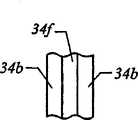
为了便于充填凹槽28,材料36a设置有完全填满凹槽28的必要性能,同时覆盖表面32带有材料36a的连续成形。在该实施例中,在达到所需的、通常最小的距离“d”之后,留有与凸起29重叠的有图案的压印层34的分部分34c,保留凸出部分34a有厚度t1,肩部34b有厚度t2和分部分有厚度t3。凸出部分34a和肩部34b在基底31的表面32上形成双高度凸起。分部分34c称为剩余层,而厚度t3为剩余厚度。根据应用情况,厚度“t1”、“t2”和“t3”可以是任何所需厚度。In order to facilitate filling of the recess 28, the material 36a is provided with the necessary properties to completely fill the recess 28, while the covering surface 32 carries a continuous formation of the material 36a. In this embodiment, after reaching the required, usually minimum, distance "d", a
参阅图2、3和4,在达到所需的距离“d”之后,辐射源22产生聚合和交联材料36a的光化辐射,形成交联的聚合材料。因此,有图案的压印层34的成分从材料36a转变成为固体的材料36c。尤其,材料36c被固化,以提供带有与有图案的模子27的表面27a的形状一致的形状的有图案的压印层34的侧面34d,如图5更清楚地所示。以这方式,在基底31上形成许多固化的双高度凸起34e。在有图案的压印层34被转变成由如图4所示的材料36c组成之后,移动图1所示的压印头18,以增加距离“d”,以致有图案的模子27和有图案的压印层34分开。Referring to Figures 2, 3 and 4, after reaching the desired distance "d", radiation source 22 produces actinic radiation that polymerizes and crosslinks material 36a, forming a crosslinked polymeric material. Thus, the composition of patterned embossed layer 34 transitions from material 36a to
将双高度凸起34e的颠倒形状转移进入基底31,用于在其中形成道路部分(未示出)和沟槽部分(未示出)。以这方式,道路部分(未示出)的尺寸被确定为凸出部分34a的尺寸的函数,以及沟槽部分(未示出)的尺寸被确定为肩部34b的尺寸的函数。因此,如图6所示,在形成固化的双高度凸起34e之后在有图案的压印层34附近设置蚀刻选择层40。基底31、有图案的压印层34和蚀刻选择层40形成多层结构38。The inverted shape of the
参阅图6,可使用任何已知加工、包括化学气相沉积(CVD)、物理气相沉积(PVD)、溅射和旋转涂复(spin-on)技术施加蚀刻选择层40。当记录图形每单位面积具有许多结构特征、即密集的有结构特征的图案时蚀刻选择层40的旋转涂复沉积可以是有利的。在该例子中,使用压印平板印刷加工、例如相对于沉积有图案的压印层34以上所讨论的那些加工沉积蚀刻选择层40。为此,除了从其形成蚀刻选择层40的材料包括硅,即为含硅聚合材料之外,可以从类似于相对于图3和4以上所述的聚合材料的一聚合材料形成蚀刻选择层40。用作为蚀刻选择层40的一示例性化合物是由约48%重量的可从宾夕法尼亚州、Morrisville的Gelest公司得到的生产代号为SIA的甲硅烷基丙烯酸;约24%重量的可从密苏里州、圣路易斯的Sigma-Aldrin公司得到的丁基丙稀酸;约24%重量的可从宾夕法尼亚州、Morrisville的Gelest公司得到的生产代码为SIB 1402的甲硅烷基二甲丙烯酸;以及约4%重量的从纽约州、Tarrytown的Ciba可得到的商标名为Darocur的自由基生成元形成。蚀刻选择层40包括第一和第二相对侧。第一侧40b面对有图案的压印层34,并具有与有图案的压印层34的外形互补的外形。第二侧面对离开有图案的压印层34的方向,形成规范表面40a。通过保证在各凸出部分34a的顶表面34f和规范表面40a之间的距离基本上相同、在各肩部34b和规范表面40a之间的距离基本上相同以及在各分部分34c的最低表面34g(如图6所示)和规范表面40a之间的距离相同,规范表面40a设置有基本规范的外形。以其对规范表面40a提供规范化外形的一方式包括使用具有将与蚀刻选择层40接触的光滑表面、即无结构特征表面127a的模子127。如以上所述,通过如图1所示沿着Z轴线移动压印头18、沿着Z轴线移动运动台20或两者,可以完成这工作。因此,使模子127与蚀刻选择层40分开,并且光化辐射撞击在蚀刻选择层40上,用于聚合,从而固化蚀刻选择层。Referring to Figure 6, the etch selective layer 40 may be applied using any known process, including chemical vapor deposition (CVD), physical vapor deposition (PVD), sputtering and spin-on techniques. Spin-on-coat deposition of the etch-selective layer 40 may be advantageous when the recorded pattern has many features per unit area, ie a densely-featured pattern. In this example, etch selective layer 40 is deposited using an imprint lithography process, such as those discussed above with respect to depositing patterned imprint layer 34 . To this end, etch selective layer 40 may be formed from a polymeric material similar to the polymeric material described above with respect to FIGS. . An exemplary compound for use as etch selective layer 40 is about 48% by weight of silyl acrylic acid available from Gelest Corporation of Morrisville, Pennsylvania under the trade designation SIA; butyl acrylic acid available from Sigma-Aldrin Corporation; about 24% by weight of silyldimethacrylic acid available from Gelest Corporation, Morrisville, Pennsylvania, under the production code SIB 1402; and about 4% by weight of Free Radical Generator Formation available under the trade name Darocur from Ciba, Tarrytown, Texas. Etch selective layer 40 includes first and second opposing sides. The first side 40b faces the patterned embossed layer 34 and has a shape that is complementary to the shape of the patterned embossed layer 34 . The second side faces away from the patterned embossed layer 34, forming a canonical surface 40a. By ensuring that the distance between the
参阅图6和7,利用覆盖层蚀刻,用于去除蚀刻选择层40的诸部分,以提供带冠表面38a的多层结构38。一示例性蚀刻加工采用CF4等离子体蚀刻,其中蚀刻气体的主要部分由CF4组成。从2003年2月23日到2月28在加利福尼亚州、Santa Clara举行的SPIE微平版印刷会议散发的白皮书内、在“分级的和快速的压印平版印刷中的进步”中Johnson等人讨论了一示例的蚀刻化学。在覆盖层蚀刻之后由各凸出部分34a的暴露的顶表面30f和保留在蚀刻选择层40上的诸部分40c的上表面形成冠表面38a。Referring to Figures 6 and 7, a blanket etch is used to remove portions of the etch selective layer 40 to provide the multilayer structure 38 with a crowned surface 38a. An exemplary etching process employsCF4 plasma etching, where the majority of the etching gas consists ofCF4 . In "Advances in Graded and Fast Imprint Lithography," Johnson et al. discuss An example etch chemistry. Crown surface 38a is formed by the exposed
参阅图7和8,冠表面38a受到非均质的蚀刻。选择非均质的蚀刻的蚀刻化学,用于对如图6所示的、处于相互重叠的有图案的压印层34的部分40c的蚀刻最小。在该例子中,利用了有图案的压印层34和蚀刻选择层40之间的硅含量的不同。尤其,使用其中氧为主要气体的等离子体蚀刻,确定了在靠近冠表面38a的诸部分40c的诸区域中将产生现场硬化的掩膜42。从2003年2月23日到2月28日在加利福尼亚州、Santa Clara举行的SPIE微平版印刷会议散发的白皮书内,在“分级的和快速的压印平版印刷中的进步”中Johnson等人讨论了一示例的蚀刻化学。作为硬化的掩膜42和蚀刻加工的非均质的结果,露出在与凸出部分34a重叠关系的基体31上的诸区域44。在该例子中,区域44是图2所示的蚀刻障碍层31b的暴露区。区域44的宽度U优选地等于图2所示的宽度W2。Referring to Figures 7 and 8, the crown surface 38a is etched non-uniformly. The etch chemistry of the non-homogeneous etch is selected to minimize the etching of the
参阅图8,在区域44暴露之后,采用例如2003年2月23日到2月28日在加利福尼亚州、Santa Clara举行的SPIE微平版印刷会方散发的白皮书内“分级的和快速的压印平版印刷中的进步”中Johnson等人讨论的采用CF4气体的一类型的氟为基的等离子蚀刻,以去除如图7所示与硬化掩膜42为重叠关系的多层结构38的诸区域,用于暴露如图9所示的诸区域45a和45b,该各区域具有宽度U’,该宽度优选地等于W2。区域45a和45b形成凹槽部分46,从区域45a和45b延伸到区域44的通路48形成道路部分。凹槽部分46形成沟槽部分,通路48形成道路部分。使用随后的蚀刻加工去除层34和40的其余部分。因此,可以同时用、例如铝、铜、钨、钛、钛—钨合金或它们的组合物等的导电材料充填道路部分和沟槽部分,形成独点50和导线52,如图10所示。Referring to FIG. 8, after the region 44 is exposed, using, for example, "Graded and Rapid Imprint Lithography" in the white paper distributed at the SPIE Microlithography Conference held in Santa Clara, California, on February 23 to February 28, 2003. A type of fluorine-based plasma etching usingCF4 gas discussed in Johnson et al., "Advances in Printing" to remove regions of the multilayer structure 38 in overlapping relationship with the
参阅图2、7和8,该加工的优点是多方面的。例如由于存在硬化的掩膜42,在部分40c和露出的顶表面30f之间相对的蚀刻速率在约1.5∶1至约100∶1的范围内。因此,可以在基底31中形成自对齐的道路和沟槽,同时精确地控制它们的尺寸。这减少了图5示出的双高度凸起34e的颠倒形状上的图案进入基底31内的转移失真。Referring to Figures 2, 7 and 8, the advantages of this process are numerous. For example due to the presence of
此外,参阅图5和9,尺寸宽度U和U’的控制变得相对独立于剩余厚度t3。聚合流体充填在有图案的模子27上的图案的速率反比于剩余厚度t3的立方。因此,可以选择剩余厚度t3,使生产量最大而不是显著增加传移失真。最后,在从基本上无硅聚合流体形成有图案的压印层34便于有图案的模子27的清洁加工,尤其考虑到通常从熔融的硅石形成有图案的模子27。Furthermore, referring to Figures 5 and 9, the control of the dimensional widths U and U' becomes relatively independent of the remaining thicknesst3 . The rate at which the polymerizing fluid fills the pattern on the patterned
参阅图2和11,本发明的附加优点是可以不需要使用蚀刻障碍层31d和31b。如众所周知的那样,通过避免使用蚀刻障碍层31d和31b,可以降低基底的总介电常数,从而使这加工适合于制造道路和沟槽,以促进高速集成电路的制造。为此,建立蚀刻条件,以致由其建立在区域140c中所示的蚀刻选择层和绝缘层131c的材料基本上对用于去除从其形成有图案的压印层34的材料的蚀刻化学不起作用。在该例子中,由其形成区域140c和绝缘层131c的材料对氧等离子体蚀刻相对地不起作用。Referring to Figures 2 and 11, an additional advantage of the present invention is that the use of etch barrier layers 31d and 31b may not be required. As is well known, by avoiding the use of etch barrier layers 31d and 31b, the overall dielectric constant of the substrate can be lowered, making the process suitable for making roads and trenches to facilitate high speed integrated circuit fabrication. To this end, etching conditions are established such that the material from which the etch selective layer and insulating
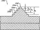
参阅图11和12,以相对于图7中的冠表面38a所讨论的方式形成的冠表面138a受到氧等离子体蚀刻。作为上述蚀刻选择性差异的结果,顶表面130f与示为M1的凸出部分134a的整个范围一起、与从而重叠在压印材料层134中的所有材料一起被去除。以这方式,形成了道路部分的一第一部分148a。Referring to Figures 11 and 12,
采用如以上所讨论的氟基化学作用进行随后的覆盖层等离子体蚀刻。覆盖层蚀刻去除图11所示的硬化掩膜142和区域140c,以露出图13所示的肩部134b。同时对于露出的肩部134b,通过去除示为M2的绝缘层131c的材料形成道路部分(未示出)的一第二部分148b。Subsequent blanket plasma etching is performed using fluorine-based chemistry as discussed above. The blanket etch removes
参阅图13和14,进行非均质的氧为基的等离子体蚀刻,以去除硬化肩部134b以及与其重叠关系的压印材料层134的材料,用于露出绝缘层131c的区域145a和145b,从而形成沟槽部分146。同时对于露出区域145a和145b,通过去除示为M3的绝缘层131c的材料形成道路部分的一第三部分148c。道路部分148a、148b、148c的组合长度形成了与沟槽部分146对齐的道路部分148。以这方式,可以制造自对齐的道路和沟槽。Referring to FIGS. 13 and 14, an inhomogeneous oxygen-based plasma etch is performed to remove the
参阅图5和15,虽然相对于形成自对齐道路和沟槽讨论了本发明,也可以应用本发明形成各种各样的多层排列结构。例如,如图5所示,与各凸起34e相关联的可以是等距离离开处于高度h1的顶表面34f和在凸起部分34a两侧的一对分开的肩部34b。或者,凸起134e可以包括围绕顶表面134f的单个肩部134b,如图16所示。Referring to Figures 5 and 15, although the invention has been discussed with respect to forming self-aligning roads and trenches, the invention can also be applied to form a variety of multilayer arrangements. For example, as shown in FIG. 5, associated with each
此外,参阅图17,各凸起234e可以包括与顶表面234f隔开的分别处于不同高度h1、h2、h3和h4的多个肩部234a、234b、234c和234d,实际上可以包括从0至n的任何数量,其中“n”是整数。为此,模子(未示出)将具有形成在它的一表面内的、将与凸起234e的形状互补的一个或多个凹槽。并且,肩部234a、234b、234c和234d可以位于顶表面234f的两侧,如图18所示。或者,肩部234a、234b、234c和234d可以同中心地设置在顶表面234f周围,如图19所示。使用凸起234e,可以将基底231形成为具有与凸起234e的形状互补的凹槽,如图20中的标号250所示。虽然基底231被示为由均质材料、例如硅形成,但是在基底231上可以包括材料的任何层数(未示出),并在上述诸层的一层或多层和/或基底231中可以形成凹槽250。并且,该诸层可以由适合于半导体加工的任何材料构成。In addition, referring to FIG. 17, each
参阅图2和21,已相对于使用具有在其中形成的多个凹槽的模子27形成基体31上的凹槽讨论了上述内容。但是,可以使用上述相同的加工形成在基底331上的诸岛部335。为此,图22所示的模子237包括从表面328a延伸的一个或多个凸起328,各凸起328具有凸出部分328b和与凸出部分隔开的在表面328a和凸出部分328b之间的肩部328c。将一层压印材料设置在基底331上,并被扩展形成如以上讨论的有图案的层334。以这方式,有图案的层334包括与模子327上的图案互补的图案。在该例子中,这造成在有图案的层334内形成一个或多个凹槽334a。Referring to Figures 2 and 21, the foregoing has been discussed with respect to forming grooves on a
参阅图22和23,因此在有图案的层334上设置蚀刻选择层340和冠表面340a以形成如以上所述形成的多层结构338。以这方式,在冠表面340a形成之后所留下的仅仅蚀刻选择层340的诸部分充填诸凹槽334a。将冠表面340a暴露于在不被凹槽334a重叠的有图案的层334的诸部分内是非常有选择性的氧等离子体蚀刻化学作用,该冠表面被去除,以露出基底331的诸区域344,如图24所示。部分地由于当暴露于使用如以上所讨论的主要由氧气构成的一化学作用的等离子体蚀刻时、蚀刻选择层340的其余部分中存在的硅所形成的硬化掩膜342,实现这了加工。Referring to Figures 22 and 23, etch
参阅图21和24,在露出诸区域344之后,使用例如以上所讨论的类型的氟基等离子体蚀刻,以去除如图23所示的多层结构338的与硬化掩膜342为重叠关系的诸区域,以露出诸区域345。尤其,在区域344和硬化掩膜342之间的蚀刻速率差异造成诸岛部335的形成。但是,应该理解按照如图22所示的模子327上的图案以这方式可以形成以上所述的任何有台阶的结构特征。并且,虽然基底331被示为由例如硅的均质材料形成,但是在基底331上可以包括材料的任何层数(未示出),并且在上述诸层的一层或多层和/或基底331中可以形成诸岛部335。而且,可以由适合于半导体加工的任何材料构成该诸层。Referring to FIGS. 21 and 24, after exposing regions 344, a fluorine-based plasma etch of the type discussed above is used to remove portions of
参阅图1和2,一示例性的辐射源22可以产生紫外线辐射。可以使用其它辐射源,例如热的、电磁的等。选择所使用的辐射以开始聚合在有图案的压印层34内的材料对于该领域的熟练人员是已知的,并通常取决于所需的特定应用情况。对辐射源22定位使有图案的模子27位于辐射源22和基底31之间。因此,可以由允许对辐射源22产生的辐射基本上能穿透的材料制造基底31和/或有图案的模子27。示例性的材料包括但不局限于熔融的硅石、石英、硅、有机聚合物、硅氧烷聚合物、硼硅酸盐玻璃、碳氟聚合物、金属和它们的组合物。Referring to Figures 1 and 2, an exemplary radiation source 22 can generate ultraviolet radiation. Other sources of radiation may be used, such as thermal, electromagnetic, etc. The selection of the radiation used to initiate polymerization of the material within the patterned embossed layer 34 is known to those skilled in the art and generally depends on the particular application desired. Radiation source 22 is positioned such that patterned
可能需要由热稳定的材料制造系统10的另件,例如这些材料在室温附近(例如摄氏25度)具有小于约百万分之一/1℃的热膨胀系数。在某些实施例中,结构材料可以具有小于约百万分之十/1℃或小于百万分之一/1℃的热膨胀系数。为此,桥支持件12、桥接件14和/或台支持件16可以由以下材料的一种和多种制成:碳化硅、商标为INVAR或SUPER INVARTM的铁合金、包括但不局限于ZERODUR陶瓷的陶瓷。此外,台架24可以被制成使系统10的其余零件与环境振动相隔离。一示例式台架24可从加利福尼亚州Irvine的Newport公司得到。It may be desirable to fabricate the other components of system 10 from thermally stable materials, eg, materials that have a coefficient of thermal expansion of less than about one part per million per 1°C near room temperature (eg, 25°C). In certain embodiments, the material of construction may have a coefficient of thermal expansion of less than about ten parts per million per 1°C or less than one part per million per 1°C. To this end, bridge support 12, bridge 14, and/or table support 16 may be fabricated from one or more of the following materials: silicon carbide, iron alloys traded as INVAR® or SUPER INVAR™ , including but not limited to Ceramics of ZERODUR(R) ceramics. Additionally, stand 24 may be made to isolate the remainder of system 10 from ambient vibrations. An exemplary rack 24 is available from Newport Corporation of Irvine, California.
参阅图1、2和3,按照所采用的独特的沉积加工,材料36a的特性对于有效地使基底31形成图案是很重要的。如以上所述,材料36a被沉积在基底上成为多个单独的和分开的珠滴36。诸珠滴36的组合容积使材料36a适当地分布在表面32的将形成有图案的压印层34的区域。因此,有图案的压印层34被扩展和与通过暴露于辐射、例如紫外线辐射而随后建立的图案同时被形成图案。作为沉积加工的结果,希望材料36a具有便于在表面32上迅速和均匀地扩展在诸珠滴36中的材料36a的某些特性,以便全部厚度t1基本均匀和全部剩余厚度t2基本均匀。Referring to Figures 1, 2 and 3, the properties of material 36a are important to effectively
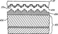
参阅图3和25,使用材料36a中的上述成份便于压印平版印刷,在基底431上包括底层456。尤其,底层456的功能是提供与有图案的压印层434的标准的界面,从而减少需要对由其形成基底431的材料定制各加工。此外,可以由带有与有图案的压印层434为相同蚀刻特性的有机材料形成底层456。以使其具有连续的、光滑的较无瑕疵的表面的方式制造底层456,该表面可以呈现对有图案的压印层434极好的粘附性。Referring to FIGS. 3 and 25 , imprint lithography is facilitated using the above composition in material 36a , including
此外,为了保证有图案的压印层434不粘附于有图案的模子27,表面27a可以被处理成带有低表面能量复层458。从而,当有图案的模子27与基底431接触时,有图案的压印层434位于底层456和复层458之间。可以利用任何已知加工施加复层458。例如,加工技术可以包括化学汽相淀积法、物理汽相淀积、原子层淀积、钎焊或许多其它技术。可以按类似方式将低表面能量复层施加于如图6所示的模子127。或者,可以通过有由其制造有图案的压印层34或蚀刻选择层40的材料中包括具有低表面能量的称为表面活化剂的化合物改进有图案的压印层34或蚀刻选择层40的释放性能。利用已知材料使该化合物分别迁移到与如图2和6所示的模子27和/或127交界的层表面。通常,表面活化剂具有与其相关联的比该层中可聚合材料的表面能量较小的表面能量。在微电子工程第61-62页(2002)上“在紫外线为基础的诺米压印平版印刷中的多次压印”内Bender等人讨论了由其形成上述表面活化剂的示例性材料和加工。表面活化剂的低表面能量提供了降低压印层34或蚀刻选择层40分别对如图2和6所示的模子27和/或127的粘附的所需的释放性能。应该理解可以与图25所示的低表面能量复层458相结合或代替它使用表面活化剂。Additionally, to ensure that the patterned embossed
以上所述的本发明的实施例是示例性的。对于以上所揭示的内容可以作出许多变化和修改,同时保持在本发明的范围内。因此,本发明的范围不应该参考以上叙述来确定,而是应该由所附权利要求书和诸等价物的它们的整个范围确定。The embodiments of the invention described above are exemplary. Many variations and modifications may be made to what has been disclosed above while remaining within the scope of the invention. Accordingly, the scope of the invention should be determined not with reference to the above description, but should be determined by the appended claims and their full scope of equivalents.
Claims (40)
Applications Claiming Priority (2)
| Application Number | Priority Date | Filing Date | Title |
|---|---|---|---|
| US10/423,642US7396475B2 (en) | 2003-04-25 | 2003-04-25 | Method of forming stepped structures employing imprint lithography |
| US10/423,642 | 2003-04-25 |
Publications (1)
| Publication Number | Publication Date |
|---|---|
| CN1791967Atrue CN1791967A (en) | 2006-06-21 |
Family
ID=33299177
Family Applications (1)
| Application Number | Title | Priority Date | Filing Date |
|---|---|---|---|
| CNA2004800139131APendingCN1791967A (en) | 2003-04-25 | 2004-04-21 | A method of forming stepped structures employing imprint lithography |
Country Status (8)
| Country | Link |
|---|---|
| US (1) | US7396475B2 (en) |
| EP (1) | EP1618602A2 (en) |
| JP (1) | JP2006524919A (en) |
| KR (1) | KR20060004679A (en) |
| CN (1) | CN1791967A (en) |
| MY (1) | MY139450A (en) |
| TW (1) | TW200502157A (en) |
| WO (1) | WO2004097518A2 (en) |
Cited By (7)
| Publication number | Priority date | Publication date | Assignee | Title |
|---|---|---|---|---|
| CN101919046A (en)* | 2007-12-31 | 2010-12-15 | 桑迪士克3D有限责任公司 | Method and apparatus for forming memory lines and vias in a three-dimensional memory array using dual damascene technology and imprint lithography |
| CN102259831A (en)* | 2010-05-27 | 2011-11-30 | 清华大学 | Three-dimensional nano structure array |
| CN101765809B (en)* | 2007-08-03 | 2012-05-16 | 佳能株式会社 | Imprint method and substrate processing method using the imprint method |
| CN102566258A (en)* | 2010-12-29 | 2012-07-11 | 中芯国际集成电路制造(上海)有限公司 | Double imprint method |
| CN102648438A (en)* | 2009-08-26 | 2012-08-22 | 分子制模股份有限公司 | functional nanoparticles |
| CN107251192A (en)* | 2015-02-27 | 2017-10-13 | 佳能株式会社 | Patterning method, the production method of substrate processing, the production method of optical module, the production method of circuit board and the production method of electronic component |
| CN107445477A (en)* | 2016-05-23 | 2017-12-08 | 陈玉彬 | Energy-saving glass and manufacturing method thereof |
Families Citing this family (166)
| Publication number | Priority date | Publication date | Assignee | Title |
|---|---|---|---|---|
| US8349241B2 (en) | 2002-10-04 | 2013-01-08 | Molecular Imprints, Inc. | Method to arrange features on a substrate to replicate features having minimal dimensional variability |
| US7186656B2 (en)* | 2004-05-21 | 2007-03-06 | Molecular Imprints, Inc. | Method of forming a recessed structure employing a reverse tone process |
| US7179396B2 (en) | 2003-03-25 | 2007-02-20 | Molecular Imprints, Inc. | Positive tone bi-layer imprint lithography method |
| US7122079B2 (en) | 2004-02-27 | 2006-10-17 | Molecular Imprints, Inc. | Composition for an etching mask comprising a silicon-containing material |
| US7323417B2 (en)* | 2004-09-21 | 2008-01-29 | Molecular Imprints, Inc. | Method of forming a recessed structure employing a reverse tone process |
| US20060108710A1 (en)* | 2004-11-24 | 2006-05-25 | Molecular Imprints, Inc. | Method to reduce adhesion between a conformable region and a mold |
| US20050160934A1 (en)* | 2004-01-23 | 2005-07-28 | Molecular Imprints, Inc. | Materials and methods for imprint lithography |
| US7307118B2 (en)* | 2004-11-24 | 2007-12-11 | Molecular Imprints, Inc. | Composition to reduce adhesion between a conformable region and a mold |
| KR100953637B1 (en)* | 2003-07-07 | 2010-04-20 | 엘지전자 주식회사 | Optical Disc and Disc Information Recording Method |
| US7136150B2 (en) | 2003-09-25 | 2006-11-14 | Molecular Imprints, Inc. | Imprint lithography template having opaque alignment marks |
| US20050156353A1 (en)* | 2004-01-15 | 2005-07-21 | Watts Michael P. | Method to improve the flow rate of imprinting material |
| US7060625B2 (en)* | 2004-01-27 | 2006-06-13 | Hewlett-Packard Development Company, L.P. | Imprint stamp |
| US7906180B2 (en)* | 2004-02-27 | 2011-03-15 | Molecular Imprints, Inc. | Composition for an etching mask comprising a silicon-containing material |
| US7435074B2 (en)* | 2004-03-13 | 2008-10-14 | International Business Machines Corporation | Method for fabricating dual damascence structures using photo-imprint lithography, methods for fabricating imprint lithography molds for dual damascene structures, materials for imprintable dielectrics and equipment for photo-imprint lithography used in dual damascence patterning |
| US20050253307A1 (en)* | 2004-05-11 | 2005-11-17 | Molecualr Imprints, Inc. | Method of patterning a conductive layer on a substrate |
| US7205244B2 (en) | 2004-09-21 | 2007-04-17 | Molecular Imprints | Patterning substrates employing multi-film layers defining etch-differential interfaces |
| US7547504B2 (en) | 2004-09-21 | 2009-06-16 | Molecular Imprints, Inc. | Pattern reversal employing thick residual layers |
| US7241395B2 (en)* | 2004-09-21 | 2007-07-10 | Molecular Imprints, Inc. | Reverse tone patterning on surfaces having planarity perturbations |
| US7041604B2 (en)* | 2004-09-21 | 2006-05-09 | Molecular Imprints, Inc. | Method of patterning surfaces while providing greater control of recess anisotropy |
| US7252777B2 (en)* | 2004-09-21 | 2007-08-07 | Molecular Imprints, Inc. | Method of forming an in-situ recessed structure |
| US20060081557A1 (en) | 2004-10-18 | 2006-04-20 | Molecular Imprints, Inc. | Low-k dielectric functional imprinting materials |
| WO2006060757A2 (en) | 2004-12-01 | 2006-06-08 | Molecular Imprints, Inc. | Eliminating printability of sub-resolution defects in imprint lithography |
| US7676088B2 (en)* | 2004-12-23 | 2010-03-09 | Asml Netherlands B.V. | Imprint lithography |
| US7691275B2 (en)* | 2005-02-28 | 2010-04-06 | Board Of Regents, The University Of Texas System | Use of step and flash imprint lithography for direct imprinting of dielectric materials for dual damascene processing |
| JP4641835B2 (en)* | 2005-03-16 | 2011-03-02 | リコー光学株式会社 | Method of manufacturing phase shifter optical element and element obtained |
| JP2006278622A (en)* | 2005-03-29 | 2006-10-12 | Tdk Corp | Method of forming irregular pattern and method of manufacturing information storage medium |
| JP4742665B2 (en)* | 2005-04-28 | 2011-08-10 | 旭硝子株式会社 | Method of manufacturing processed substrate processed by etching |
| JP4736522B2 (en)* | 2005-04-28 | 2011-07-27 | 旭硝子株式会社 | Method of manufacturing processed substrate processed by etching |
| US7256131B2 (en)* | 2005-07-19 | 2007-08-14 | Molecular Imprints, Inc. | Method of controlling the critical dimension of structures formed on a substrate |
| US8808808B2 (en)* | 2005-07-22 | 2014-08-19 | Molecular Imprints, Inc. | Method for imprint lithography utilizing an adhesion primer layer |
| US8846195B2 (en)* | 2005-07-22 | 2014-09-30 | Canon Nanotechnologies, Inc. | Ultra-thin polymeric adhesion layer |
| US8557351B2 (en)* | 2005-07-22 | 2013-10-15 | Molecular Imprints, Inc. | Method for adhering materials together |
| US7419611B2 (en)* | 2005-09-02 | 2008-09-02 | International Business Machines Corporation | Processes and materials for step and flash imprint lithography |
| US7259102B2 (en)* | 2005-09-30 | 2007-08-21 | Molecular Imprints, Inc. | Etching technique to planarize a multi-layer structure |
| US8142703B2 (en) | 2005-10-05 | 2012-03-27 | Molecular Imprints, Inc. | Imprint lithography method |
| FR2893018B1 (en)* | 2005-11-09 | 2008-03-14 | Commissariat Energie Atomique | METHOD OF FORMING MEDIA HAVING PATTERNS, SUCH AS LITHOGRAPHIC MASKS |
| US7670530B2 (en) | 2006-01-20 | 2010-03-02 | Molecular Imprints, Inc. | Patterning substrates employing multiple chucks |
| MY144847A (en) | 2005-12-08 | 2011-11-30 | Molecular Imprints Inc | Method and system for double-sided patterning of substrates |
| US7517211B2 (en) | 2005-12-21 | 2009-04-14 | Asml Netherlands B.V. | Imprint lithography |
| GB2436163A (en)* | 2006-03-10 | 2007-09-19 | Seiko Epson Corp | Device fabrication by ink-jet printing materials into bank structures, and embossing tool |
| JP4861044B2 (en)* | 2006-04-18 | 2012-01-25 | キヤノン株式会社 | Substrate processing method and method for manufacturing member having pattern region |
| JP4810319B2 (en)* | 2006-06-09 | 2011-11-09 | キヤノン株式会社 | Processing apparatus and device manufacturing method |
| DE102006030267B4 (en)* | 2006-06-30 | 2009-04-16 | Advanced Micro Devices, Inc., Sunnyvale | Nano embossing technique with increased flexibility in terms of adjustment and shaping of structural elements |
| US7718077B1 (en)* | 2006-07-25 | 2010-05-18 | Hewlett-Packard Development Company, L.P. | Fabricating a structure usable in an imprint lithographic process |
| US20080102380A1 (en)* | 2006-10-30 | 2008-05-01 | Mangat Pawitter S | High density lithographic process |
| US20080264553A1 (en)* | 2007-04-27 | 2008-10-30 | Hewlett-Packard Development Company Lp | Embossing |
| US7794614B2 (en)* | 2007-05-29 | 2010-09-14 | Qimonda Ag | Methods for generating sublithographic structures |
| US8142702B2 (en)* | 2007-06-18 | 2012-03-27 | Molecular Imprints, Inc. | Solvent-assisted layer formation for imprint lithography |
| US7837907B2 (en)* | 2007-07-20 | 2010-11-23 | Molecular Imprints, Inc. | Alignment system and method for a substrate in a nano-imprint process |
| US7795132B2 (en)* | 2007-07-31 | 2010-09-14 | Molecular Imprints, Inc. | Self-aligned cross-point memory fabrication |
| US20090053535A1 (en)* | 2007-08-24 | 2009-02-26 | Molecular Imprints, Inc. | Reduced Residual Formation in Etched Multi-Layer Stacks |
| SG185929A1 (en)* | 2007-11-21 | 2012-12-28 | Molecular Imprints Inc | Porous template and imprinting stack for nano-imprint lithography |
| US7906274B2 (en)* | 2007-11-21 | 2011-03-15 | Molecular Imprints, Inc. | Method of creating a template employing a lift-off process |
| EP2215661A1 (en)* | 2007-11-28 | 2010-08-11 | Molecular Imprints, Inc. | Nanostructured organic solar cells |
| US20090147237A1 (en)* | 2007-12-05 | 2009-06-11 | Molecular Imprints, Inc. | Spatial Phase Feature Location |
| US20090166317A1 (en)* | 2007-12-26 | 2009-07-02 | Canon Kabushiki Kaisha | Method of processing substrate by imprinting |
| US20100301449A1 (en)* | 2007-12-31 | 2010-12-02 | Sandisk 3D Llc | Methods and apparatus for forming line and pillar structures for three dimensional memory arrays using a double subtractive process and imprint lithography |
| US20100072671A1 (en)* | 2008-09-25 | 2010-03-25 | Molecular Imprints, Inc. | Nano-imprint lithography template fabrication and treatment |
| US8470188B2 (en)* | 2008-10-02 | 2013-06-25 | Molecular Imprints, Inc. | Nano-imprint lithography templates |
| US20100090341A1 (en)* | 2008-10-14 | 2010-04-15 | Molecular Imprints, Inc. | Nano-patterned active layers formed by nano-imprint lithography |
| US8415010B2 (en)* | 2008-10-20 | 2013-04-09 | Molecular Imprints, Inc. | Nano-imprint lithography stack with enhanced adhesion between silicon-containing and non-silicon containing layers |
| US8075299B2 (en)* | 2008-10-21 | 2011-12-13 | Molecular Imprints, Inc. | Reduction of stress during template separation |
| US20100095862A1 (en)* | 2008-10-22 | 2010-04-22 | Molecular Imprints, Inc. | Double Sidewall Angle Nano-Imprint Template |
| US20100104852A1 (en)* | 2008-10-23 | 2010-04-29 | Molecular Imprints, Inc. | Fabrication of High-Throughput Nano-Imprint Lithography Templates |
| US8652393B2 (en) | 2008-10-24 | 2014-02-18 | Molecular Imprints, Inc. | Strain and kinetics control during separation phase of imprint process |
| US8361546B2 (en)* | 2008-10-30 | 2013-01-29 | Molecular Imprints, Inc. | Facilitating adhesion between substrate and patterned layer |
| US8309008B2 (en)* | 2008-10-30 | 2012-11-13 | Molecular Imprints, Inc. | Separation in an imprint lithography process |
| US20100112220A1 (en)* | 2008-11-03 | 2010-05-06 | Molecular Imprints, Inc. | Dispense system set-up and characterization |
| US20100109205A1 (en)* | 2008-11-04 | 2010-05-06 | Molecular Imprints, Inc. | Photocatalytic reactions in nano-imprint lithography processes |
| US20100109195A1 (en) | 2008-11-05 | 2010-05-06 | Molecular Imprints, Inc. | Release agent partition control in imprint lithography |
| WO2010111307A1 (en)* | 2009-03-23 | 2010-09-30 | Intevac, Inc. | A process for optimization of island to trench ratio in patterned media |
| US9164375B2 (en) | 2009-06-19 | 2015-10-20 | Canon Nanotechnologies, Inc. | Dual zone template chuck |
| US8913230B2 (en) | 2009-07-02 | 2014-12-16 | Canon Nanotechnologies, Inc. | Chucking system with recessed support feature |
| US20110031650A1 (en)* | 2009-08-04 | 2011-02-10 | Molecular Imprints, Inc. | Adjacent Field Alignment |
| US20110030770A1 (en) | 2009-08-04 | 2011-02-10 | Molecular Imprints, Inc. | Nanostructured organic solar cells |
| US20110048518A1 (en)* | 2009-08-26 | 2011-03-03 | Molecular Imprints, Inc. | Nanostructured thin film inorganic solar cells |
| US20110084417A1 (en) | 2009-10-08 | 2011-04-14 | Molecular Imprints, Inc. | Large area linear array nanoimprinting |
| US8227339B2 (en) | 2009-11-02 | 2012-07-24 | International Business Machines Corporation | Creation of vias and trenches with different depths |
| TWI386761B (en)* | 2009-11-06 | 2013-02-21 | Univ Nat Cheng Kung | Multi-step contact printing process |
| WO2011066450A2 (en) | 2009-11-24 | 2011-06-03 | Molecular Imprints, Inc. | Adhesion layers in nanoimprint lithography |
| US20110140304A1 (en) | 2009-12-10 | 2011-06-16 | Molecular Imprints, Inc. | Imprint lithography template |
| US8616873B2 (en)* | 2010-01-26 | 2013-12-31 | Molecular Imprints, Inc. | Micro-conformal templates for nanoimprint lithography |
| US8980751B2 (en) | 2010-01-27 | 2015-03-17 | Canon Nanotechnologies, Inc. | Methods and systems of material removal and pattern transfer |
| US20110180127A1 (en)* | 2010-01-28 | 2011-07-28 | Molecular Imprints, Inc. | Solar cell fabrication by nanoimprint lithography |
| US8691134B2 (en)* | 2010-01-28 | 2014-04-08 | Molecular Imprints, Inc. | Roll-to-roll imprint lithography and purging system |
| TW201144091A (en) | 2010-01-29 | 2011-12-16 | Molecular Imprints Inc | Ultra-compliant nanoimprint lithography templates |
| WO2011094672A2 (en) | 2010-01-29 | 2011-08-04 | Molecular Imprints, Inc. | Nanoimprint lithography processes for forming nanoparticles |
| WO2011097514A2 (en) | 2010-02-05 | 2011-08-11 | Molecular Imprints, Inc. | Templates having high contrast alignment marks |
| JP5848263B2 (en) | 2010-02-09 | 2016-01-27 | モレキュラー・インプリンツ・インコーポレーテッド | Process gas confinement for nanoimprint |
| EP2564271B1 (en) | 2010-04-27 | 2015-12-16 | Canon Nanotechnologies, Inc. | Separation control substrate/template for nanoimprint lithography |
| WO2011143327A2 (en) | 2010-05-11 | 2011-11-17 | Molecular Imprints, Inc. | Nanostructured solar cell |
| US8541053B2 (en) | 2010-07-08 | 2013-09-24 | Molecular Imprints, Inc. | Enhanced densification of silicon oxide layers |
| US8891080B2 (en) | 2010-07-08 | 2014-11-18 | Canon Nanotechnologies, Inc. | Contaminate detection and substrate cleaning |
| EP2618978B1 (en) | 2010-09-24 | 2016-11-09 | Canon Nanotechnologies, Inc. | High contrast alignment marks through multiple stage imprinting |
| KR102046933B1 (en) | 2010-11-05 | 2019-11-20 | 캐논 나노테크놀로지즈 인코퍼레이티드 | Patterning of non-convex shaped nanostructures |
| CN103282303A (en) | 2010-11-05 | 2013-09-04 | 分子制模股份有限公司 | Nanoimprint lithography formation of functional nanoparticles using dual release layers |
| US8926888B2 (en) | 2011-02-25 | 2015-01-06 | Board Of Regents, The University Of Texas System | Fluorinated silazane release agents in nanoimprint lithography |
| US8967992B2 (en) | 2011-04-25 | 2015-03-03 | Canon Nanotechnologies, Inc. | Optically absorptive material for alignment marks |
| JP6324318B2 (en) | 2011-12-19 | 2018-05-16 | キャノン・ナノテクノロジーズ・インコーポレーテッド | Method for producing a seamless large area master template for imprint lithography |
| BR102012016393A2 (en) | 2012-07-02 | 2015-04-07 | Rexam Beverage Can South America S A | Can printing device, can printing process, printed can and blanket |
| US20140014621A1 (en)* | 2012-07-16 | 2014-01-16 | Zhaoning Yu | Analysis of pattern features |
| KR102170524B1 (en) | 2013-03-15 | 2020-10-27 | 캐논 나노테크놀로지즈 인코퍼레이티드 | Nano imprinting with reusable polymer template with metallic or oxide coating |
| US9555616B2 (en) | 2013-06-11 | 2017-01-31 | Ball Corporation | Variable printing process using soft secondary plates and specialty inks |
| WO2014201005A1 (en) | 2013-06-11 | 2014-12-18 | Ball Corporation | Printing process using soft photopolymer plates |
| US9651862B2 (en) | 2013-07-12 | 2017-05-16 | Canon Nanotechnologies, Inc. | Drop pattern generation for imprint lithography with directionally-patterned templates |
| US10160145B2 (en)* | 2013-09-03 | 2018-12-25 | STRATEC CONSUMABLES GmbH | Microfluidic device |
| WO2015070054A1 (en) | 2013-11-08 | 2015-05-14 | Canon Nanotechnologies, Inc. | Low contact imprint lithography template chuck system for improved overlay correction |
| US10124529B2 (en) | 2013-12-10 | 2018-11-13 | Canon Nanotechnologies, Inc. | Imprint lithography template and method for zero-gap imprinting |
| US9514950B2 (en) | 2013-12-30 | 2016-12-06 | Canon Nanotechnologies, Inc. | Methods for uniform imprint pattern transfer of sub-20 nm features |
| CN106030756B (en) | 2013-12-31 | 2021-01-22 | 佳能纳米技术公司 | Asymmetric template shape adjustment for local area imprinting |
| KR102279239B1 (en) | 2014-07-25 | 2021-07-19 | 삼성전자주식회사 | Method of transferring reverse pattern using imprint process |
| US10086602B2 (en) | 2014-11-10 | 2018-10-02 | Rexam Beverage Can South America | Method and apparatus for printing metallic beverage container bodies |
| PL3028856T3 (en) | 2014-12-04 | 2019-10-31 | Ball Beverage Packaging Europe Ltd | Printing apparatus |
| JP2016162863A (en)* | 2015-02-27 | 2016-09-05 | キヤノン株式会社 | Pattern formation method, manufacturing method for processed substrate, manufacturing method for optical component, manufacturing method for circuit board, and manufacturing method for electronic component |
| RU2593633C1 (en)* | 2015-05-14 | 2016-08-10 | Федеральное государственное автономное образовательное учреждение высшего образования "Дальневосточный федеральный университет" | Method of forming ordered structures on surface of semiconductor substrates |
| JP6437387B2 (en)* | 2015-05-25 | 2018-12-12 | 東芝メモリ株式会社 | Substrate flattening method |
| EP3347410B1 (en)* | 2015-09-08 | 2024-06-19 | Canon Kabushiki Kaisha | Substrate pretreatment and etch uniformity in nanoimprint lithography |
| US10488753B2 (en) | 2015-09-08 | 2019-11-26 | Canon Kabushiki Kaisha | Substrate pretreatment and etch uniformity in nanoimprint lithography |
| US20170066208A1 (en) | 2015-09-08 | 2017-03-09 | Canon Kabushiki Kaisha | Substrate pretreatment for reducing fill time in nanoimprint lithography |
| JP6646888B2 (en)* | 2015-09-09 | 2020-02-14 | 大日本印刷株式会社 | Convex structure, concave structure, and method of manufacturing convex structure |
| US10131134B2 (en) | 2015-10-30 | 2018-11-20 | Canon Kabushiki Kaisha | System and method for discharging electrostatic charge in nanoimprint lithography processes |
| US10211051B2 (en) | 2015-11-13 | 2019-02-19 | Canon Kabushiki Kaisha | Method of reverse tone patterning |
| US10654216B2 (en) | 2016-03-30 | 2020-05-19 | Canon Kabushiki Kaisha | System and methods for nanoimprint lithography |
| US10134588B2 (en) | 2016-03-31 | 2018-11-20 | Canon Kabushiki Kaisha | Imprint resist and substrate pretreatment for reducing fill time in nanoimprint lithography |
| US10095106B2 (en) | 2016-03-31 | 2018-10-09 | Canon Kabushiki Kaisha | Removing substrate pretreatment compositions in nanoimprint lithography |
| US10620539B2 (en) | 2016-03-31 | 2020-04-14 | Canon Kabushiki Kaisha | Curing substrate pretreatment compositions in nanoimprint lithography |
| US10549921B2 (en) | 2016-05-19 | 2020-02-04 | Rexam Beverage Can Company | Beverage container body decorator inspection apparatus |
| US10189188B2 (en) | 2016-05-20 | 2019-01-29 | Canon Kabushiki Kaisha | Nanoimprint lithography adhesion layer |
| US9993962B2 (en)* | 2016-05-23 | 2018-06-12 | Canon Kabushiki Kaisha | Method of imprinting to correct for a distortion within an imprint system |
| CN117976523A (en) | 2016-05-25 | 2024-05-03 | 大日本印刷株式会社 | Method for manufacturing imprint template substrate, method for manufacturing imprint template, and template |
| US10509313B2 (en) | 2016-06-28 | 2019-12-17 | Canon Kabushiki Kaisha | Imprint resist with fluorinated photoinitiator and substrate pretreatment for reducing fill time in nanoimprint lithography |
| US11034145B2 (en) | 2016-07-20 | 2021-06-15 | Ball Corporation | System and method for monitoring and adjusting a decorator for containers |
| RU2701243C1 (en) | 2016-07-20 | 2019-09-25 | Бол Корпорейшн | System and method of adjusting paint assembly of printing machine on cylinders and tubes |
| US10739705B2 (en) | 2016-08-10 | 2020-08-11 | Ball Corporation | Method and apparatus of decorating a metallic container by digital printing to a transfer blanket |
| WO2018031814A1 (en) | 2016-08-10 | 2018-02-15 | Ball Corporation | Method and apparatus of decorating a metallic container by digital printing to a transfer blanket |
| US10838298B2 (en) | 2016-09-21 | 2020-11-17 | Molecular Imprints, Inc. | Microlithographic fabrication of structures |
| US9761450B1 (en)* | 2016-09-26 | 2017-09-12 | International Business Machines Corporation | Forming a fin cut in a hardmask |
| US10035296B2 (en) | 2016-10-13 | 2018-07-31 | Canon Kabushiki Kaisha | Methods for controlling spread of imprint material |
| KR102326522B1 (en) | 2016-10-18 | 2021-11-12 | 몰레큘러 임프린츠 인코퍼레이티드 | Microlithographic fabrication of structures |
| US10549313B2 (en) | 2016-10-31 | 2020-02-04 | Canon Kabushiki Kaisha | Edge field imprint lithography |
| US10627715B2 (en) | 2016-10-31 | 2020-04-21 | Canon Kabushiki Kaisha | Method for separating a nanoimprint template from a substrate |
| US11454883B2 (en) | 2016-11-14 | 2022-09-27 | Canon Kabushiki Kaisha | Template replication |
| US10969680B2 (en) | 2016-11-30 | 2021-04-06 | Canon Kabushiki Kaisha | System and method for adjusting a position of a template |
| JP6685886B2 (en)* | 2016-12-08 | 2020-04-22 | キオクシア株式会社 | Template and method for manufacturing semiconductor device |
| US10578984B2 (en) | 2016-12-20 | 2020-03-03 | Canon Kabushiki Kaisha | Adaptive chucking system |
| US10712660B2 (en)* | 2016-12-21 | 2020-07-14 | Canon Kabushiki Kaisha | Template for imprint lithography including a recession and an apparatus and method of using the template |
| US10079152B1 (en) | 2017-02-24 | 2018-09-18 | Canon Kabushiki Kaisha | Method for forming planarized etch mask structures over existing topography |
| US9971249B1 (en) | 2017-02-27 | 2018-05-15 | Canon Kabushiki Kaisha | Method and system for controlled ultraviolet light exposure |
| US10317793B2 (en) | 2017-03-03 | 2019-06-11 | Canon Kabushiki Kaisha | Substrate pretreatment compositions for nanoimprint lithography |
| US10303049B2 (en) | 2017-03-22 | 2019-05-28 | Canon Kabushiki Kaisha | Reducing electric charge in imprint lithography |
| US10534259B2 (en) | 2017-03-28 | 2020-01-14 | Canon Kabushiki Kaisha | Method and system for imprint force control |
| US10866510B2 (en) | 2017-07-31 | 2020-12-15 | Canon Kabushiki Kaisha | Overlay improvement in nanoimprint lithography |
| US10996560B2 (en) | 2017-07-31 | 2021-05-04 | Canon Kabushiki Kaisha | Real-time correction of template deformation in nanoimprint lithography |
| US10606170B2 (en) | 2017-09-14 | 2020-03-31 | Canon Kabushiki Kaisha | Template for imprint lithography and methods of making and using the same |
| US10935883B2 (en) | 2017-09-29 | 2021-03-02 | Canon Kabushiki Kaisha | Nanoimprint template with light blocking material and method of fabrication |
| US11036130B2 (en) | 2017-10-19 | 2021-06-15 | Canon Kabushiki Kaisha | Drop placement evaluation |
| US10788749B2 (en) | 2017-11-30 | 2020-09-29 | Canon Kabushiki Kaisha | System and method for improving the throughput of a nanoimprint system |
| US10409178B2 (en) | 2017-12-18 | 2019-09-10 | Canon Kabushiki Kaisha | Alignment control in nanoimprint lithography based on real-time system identification |
| US10996561B2 (en) | 2017-12-26 | 2021-05-04 | Canon Kabushiki Kaisha | Nanoimprint lithography with a six degrees-of-freedom imprint head module |
| JP2020035924A (en)* | 2018-08-30 | 2020-03-05 | キオクシア株式会社 | Original |
| JP7414597B2 (en) | 2020-03-12 | 2024-01-16 | キオクシア株式会社 | Wiring formation method |
| JP2021145076A (en) | 2020-03-13 | 2021-09-24 | キオクシア株式会社 | Original plate and method for manufacturing semiconductor device |
| US11815811B2 (en) | 2021-03-23 | 2023-11-14 | Canon Kabushiki Kaisha | Magnification ramp scheme to mitigate template slippage |
| US12124165B2 (en) | 2021-10-25 | 2024-10-22 | Canon Kabushiki Kaisha | Apparatus and method for optimizing actuator forces |
| JP2025068357A (en) | 2023-10-16 | 2025-04-28 | 信越化学工業株式会社 | Composition for forming resist underlayer film, resist underlayer film, method for manufacturing resist underlayer film, patterning process, and method for manufacturing semiconductor device |
| JP2025070979A (en) | 2023-10-20 | 2025-05-02 | 信越化学工業株式会社 | Composition for forming resist underlayer film, resist underlayer film, method for producing resist underlayer film, pattern forming method, and method for producing semiconductor device |
Family Cites Families (238)
| Publication number | Priority date | Publication date | Assignee | Title |
|---|---|---|---|---|
| US3810874A (en) | 1969-03-10 | 1974-05-14 | Minnesota Mining & Mfg | Polymers prepared from poly(perfluoro-alkylene oxide) compounds |
| US3783520A (en) | 1970-09-28 | 1974-01-08 | Bell Telephone Labor Inc | High accuracy alignment procedure utilizing moire patterns |
| FR2325018A1 (en) | 1975-06-23 | 1977-04-15 | Ibm | INTERVAL MEASURING DEVICE FOR DEFINING THE DISTANCE BETWEEN TWO OR MORE FACES |
| IT1068535B (en) | 1975-11-03 | 1985-03-21 | Ibm | APPARATUS AND GRAPHIC ELECTROLYTE PROCESS |
| DE2800476A1 (en) | 1977-01-07 | 1978-07-13 | Instruments Sa | Mass prodn. method for grids, graticules etc. - using revolving drum, belt carrying resin and UV light source for polymerisation process |
| JPS577931Y2 (en) | 1977-06-03 | 1982-02-16 | ||
| US4201800A (en) | 1978-04-28 | 1980-05-06 | International Business Machines Corp. | Hardened photoresist master image mask process |
| JPS6053675B2 (en) | 1978-09-20 | 1985-11-27 | 富士写真フイルム株式会社 | Spin coating method |
| JPS605935Y2 (en) | 1978-12-05 | 1985-02-25 | アイダエンジニアリング株式会社 | feeder moving device |
| JPS5884808A (en) | 1981-11-13 | 1983-05-21 | Nippon Synthetic Chem Ind Co Ltd:The | Preparation of resinous material |
| US4426247A (en) | 1982-04-12 | 1984-01-17 | Nippon Telegraph & Telephone Public Corporation | Method for forming micropattern |
| FR2538923A1 (en) | 1982-12-30 | 1984-07-06 | Thomson Csf | METHOD AND DEVICE FOR OPTICALLY ALIGNING PATTERNS IN TWO PLANS RECONCILED IN AN EXPOSURE APPARATUS COMPRISING A DIVERGENT RADIATION SOURCE |
| US4507331A (en) | 1983-12-12 | 1985-03-26 | International Business Machines Corporation | Dry process for forming positive tone micro patterns |
| US4512848A (en)* | 1984-02-06 | 1985-04-23 | Exxon Research And Engineering Co. | Procedure for fabrication of microstructures over large areas using physical replication |
| US4552833A (en) | 1984-05-14 | 1985-11-12 | International Business Machines Corporation | Radiation sensitive and oxygen plasma developable resist |
| US4614667A (en) | 1984-05-21 | 1986-09-30 | Minnesota Mining And Manufacturing Company | Composite low surface energy liner of perfluoropolyether |
| US4908298A (en) | 1985-03-19 | 1990-03-13 | International Business Machines Corporation | Method of creating patterned multilayer films for use in production of semiconductor circuits and systems |
| EP0245461A1 (en) | 1985-11-18 | 1987-11-19 | EASTMAN KODAK COMPANY (a New Jersey corporation) | Process for making optical recording media |
| EP0228671A1 (en) | 1985-12-23 | 1987-07-15 | General Electric Company | Method for the production of a coated substrate with controlled surface characteristics |
| US4657845A (en) | 1986-01-14 | 1987-04-14 | International Business Machines Corporation | Positive tone oxygen plasma developable photoresist |
| US4692205A (en) | 1986-01-31 | 1987-09-08 | International Business Machines Corporation | Silicon-containing polyimides as oxygen etch stop and dual dielectric coatings |
| US4737425A (en) | 1986-06-10 | 1988-04-12 | International Business Machines Corporation | Patterned resist and process |
| KR900004269B1 (en) | 1986-06-11 | 1990-06-18 | 가부시기가이샤 도시바 | Method and device for positioing 1st body and 2nd body |
| EP0255303B1 (en) | 1986-07-25 | 1989-10-11 | Oki Electric Industry Company, Limited | Negative resist material, method for its manufacture and method for using it |
| JPS6376330A (en) | 1986-09-18 | 1988-04-06 | Oki Electric Ind Co Ltd | Manufacture of semiconductor device |
| FR2604553A1 (en) | 1986-09-29 | 1988-04-01 | Rhone Poulenc Chimie | RIGID POLYMER SUBSTRATE FOR OPTICAL DISC AND OPTICAL DISCS OBTAINED FROM THE SUBSTRATE |
| US4707218A (en) | 1986-10-28 | 1987-11-17 | International Business Machines Corporation | Lithographic image size reduction |
| US4931351A (en) | 1987-01-12 | 1990-06-05 | Eastman Kodak Company | Bilayer lithographic process |
| US5736424A (en) | 1987-02-27 | 1998-04-07 | Lucent Technologies Inc. | Device fabrication involving planarization |
| US6391798B1 (en) | 1987-02-27 | 2002-05-21 | Agere Systems Guardian Corp. | Process for planarization a semiconductor substrate |
| JPS63138730U (en) | 1987-03-03 | 1988-09-13 | ||
| US4731155A (en) | 1987-04-15 | 1988-03-15 | General Electric Company | Process for forming a lithographic mask |
| US4808511A (en) | 1987-05-19 | 1989-02-28 | International Business Machines Corporation | Vapor phase photoresist silylation process |
| KR930000293B1 (en) | 1987-10-26 | 1993-01-15 | 마쯔시다덴기산교 가부시기가이샤 | Fine pattern formation method |
| US5028366A (en) | 1988-01-12 | 1991-07-02 | Air Products And Chemicals, Inc. | Water based mold release compositions for making molded polyurethane foam |
| JPH01196749A (en) | 1988-01-30 | 1989-08-08 | Hoya Corp | Manufacture of substrate for optical information recording medium |
| US4891303A (en) | 1988-05-26 | 1990-01-02 | Texas Instruments Incorporated | Trilayer microlithographic process using a silicon-based resist as the middle layer |
| JPH0269936A (en) | 1988-07-28 | 1990-03-08 | Siemens Ag | Method for forming resin structures on semiconductor materials |
| US4921778A (en) | 1988-07-29 | 1990-05-01 | Shipley Company Inc. | Photoresist pattern fabrication employing chemically amplified metalized material |
| US5108875A (en) | 1988-07-29 | 1992-04-28 | Shipley Company Inc. | Photoresist pattern fabrication employing chemically amplified metalized material |
| EP0355496A3 (en) | 1988-08-15 | 1990-10-10 | Sumitomo Heavy Industries Co., Ltd. | Position detector employing a sector fresnel zone plate |
| JP2546350B2 (en) | 1988-09-09 | 1996-10-23 | キヤノン株式会社 | Alignment device |
| US4964945A (en) | 1988-12-09 | 1990-10-23 | Minnesota Mining And Manufacturing Company | Lift off patterning process on a flexible substrate |
| US5439766A (en) | 1988-12-30 | 1995-08-08 | International Business Machines Corporation | Composition for photo imaging |
| JPH0292603U (en) | 1989-01-09 | 1990-07-23 | ||
| JPH02192045A (en) | 1989-01-20 | 1990-07-27 | Fujitsu Ltd | Production of optical disk substrate |
| CA2010169A1 (en) | 1989-02-21 | 1990-08-21 | Masakazu Uekita | Multi-layer resist |
| US4999280A (en) | 1989-03-17 | 1991-03-12 | International Business Machines Corporation | Spray silylation of photoresist images |
| US5169494A (en) | 1989-03-27 | 1992-12-08 | Matsushita Electric Industrial Co., Ltd. | Fine pattern forming method |
| DE59010728D1 (en) | 1989-04-24 | 1997-07-31 | Siemens Ag | Process for producing etch-resistant structures |
| JP3001607B2 (en) | 1989-04-24 | 2000-01-24 | シーメンス、アクチエンゲゼルシヤフト | Dimensionally stable structure transfer method in two-layer method |
| US5110514A (en) | 1989-05-01 | 1992-05-05 | Soane Technologies, Inc. | Controlled casting of a shrinkable material |
| US5053318A (en) | 1989-05-18 | 1991-10-01 | Shipley Company Inc. | Plasma processing with metal mask integration |
| CA2011927C (en) | 1989-06-02 | 1996-12-24 | Alan Lee Sidman | Microlithographic method for producing thick, vertically-walled photoresist patterns |
| US4919748A (en) | 1989-06-30 | 1990-04-24 | At&T Bell Laboratories | Method for tapered etching |
| JP2704001B2 (en) | 1989-07-18 | 1998-01-26 | キヤノン株式会社 | Position detection device |
| DE4031637C2 (en) | 1989-10-06 | 1997-04-10 | Toshiba Kawasaki Kk | Arrangement for measuring a displacement between two objects |
| US5362606A (en) | 1989-10-18 | 1994-11-08 | Massachusetts Institute Of Technology | Positive resist pattern formation through focused ion beam exposure and surface barrier silylation |
| US5139925A (en) | 1989-10-18 | 1992-08-18 | Massachusetts Institute Of Technology | Surface barrier silylation of novolak film without photoactive additive patterned with 193 nm excimer laser |
| JP3197010B2 (en) | 1990-03-05 | 2001-08-13 | 株式会社東芝 | Interval setting method and interval setting device |
| US5328810A (en) | 1990-05-07 | 1994-07-12 | Micron Technology, Inc. | Method for reducing, by a factor or 2-N, the minimum masking pitch of a photolithographic process |
| JP2586692B2 (en) | 1990-05-24 | 1997-03-05 | 松下電器産業株式会社 | Pattern forming material and pattern forming method |
| JP2524436B2 (en) | 1990-09-18 | 1996-08-14 | インターナショナル・ビジネス・マシーンズ・コーポレイション | Surface treatment method |
| DE4029912A1 (en) | 1990-09-21 | 1992-03-26 | Philips Patentverwaltung | METHOD FOR FORMING AT LEAST ONE TRENCH IN A SUBSTRATE LAYER |
| US5314772A (en) | 1990-10-09 | 1994-05-24 | Arizona Board Of Regents | High resolution, multi-layer resist for microlithography and method therefor |
| US5240878A (en) | 1991-04-26 | 1993-08-31 | International Business Machines Corporation | Method for forming patterned films on a substrate |
| US5212147A (en) | 1991-05-15 | 1993-05-18 | Hewlett-Packard Company | Method of forming a patterned in-situ high Tc superconductive film |
| US5206983A (en) | 1991-06-24 | 1993-05-04 | Wisconsin Alumni Research Foundation | Method of manufacturing micromechanical devices |
| US5421981A (en) | 1991-06-26 | 1995-06-06 | Ppg Industries, Inc. | Electrochemical sensor storage device |
| EP0524759A1 (en) | 1991-07-23 | 1993-01-27 | AT&T Corp. | Device fabrication process |
| US5242711A (en) | 1991-08-16 | 1993-09-07 | Rockwell International Corp. | Nucleation control of diamond films by microlithographic patterning |
| JPH0580530A (en)* | 1991-09-24 | 1993-04-02 | Hitachi Ltd | Production of thin film pattern |
| US5263073A (en) | 1991-12-20 | 1993-11-16 | Board Of Supervisors Of Louisiana State University And Agricultural And Mechanical College | Scanning systems for high resolution E-beam and X-ray lithography |
| US5244818A (en) | 1992-04-08 | 1993-09-14 | Georgia Tech Research Corporation | Processes for lift-off of thin film materials and for the fabrication of three dimensional integrated circuits |
| US5545367A (en) | 1992-04-15 | 1996-08-13 | Soane Technologies, Inc. | Rapid prototype three dimensional stereolithography |
| US5376810A (en) | 1992-06-26 | 1994-12-27 | California Institute Of Technology | Growth of delta-doped layers on silicon CCD/S for enhanced ultraviolet response |
| US5601641A (en) | 1992-07-21 | 1997-02-11 | Tse Industries, Inc. | Mold release composition with polybutadiene and method of coating a mold core |
| US5431777A (en) | 1992-09-17 | 1995-07-11 | International Business Machines Corporation | Methods and compositions for the selective etching of silicon |
| TW227628B (en) | 1992-12-10 | 1994-08-01 | Samsung Electronics Co Ltd | |
| DE69405451T2 (en) | 1993-03-16 | 1998-03-12 | Koninkl Philips Electronics Nv | Method and device for producing a structured relief image from cross-linked photoresist on a flat substrate surface |
| US5380474A (en) | 1993-05-20 | 1995-01-10 | Sandia Corporation | Methods for patterned deposition on a substrate |
| US5324683A (en) | 1993-06-02 | 1994-06-28 | Motorola, Inc. | Method of forming a semiconductor structure having an air region |
| JP2837063B2 (en) | 1993-06-04 | 1998-12-14 | シャープ株式会社 | Method of forming resist pattern |
| US5389696A (en) | 1993-09-17 | 1995-02-14 | Miles Inc. | Process for the production of molded products using internal mold release agents |
| US5512131A (en) | 1993-10-04 | 1996-04-30 | President And Fellows Of Harvard College | Formation of microstamped patterns on surfaces and derivative articles |
| US6776094B1 (en) | 1993-10-04 | 2004-08-17 | President & Fellows Of Harvard College | Kit For Microcontact Printing |
| US5776748A (en) | 1993-10-04 | 1998-07-07 | President And Fellows Of Harvard College | Method of formation of microstamped patterns on plates for adhesion of cells and other biological materials, devices and uses therefor |
| US5900160A (en) | 1993-10-04 | 1999-05-04 | President And Fellows Of Harvard College | Methods of etching articles via microcontact printing |
| NL9401260A (en) | 1993-11-12 | 1995-06-01 | Cornelis Johannes Maria Van Ri | Membrane for microfiltration, ultrafiltration, gas separation and catalysis, method for manufacturing such a membrane, mold for manufacturing such a membrane, as well as various separation systems comprising such a membrane. |
| KR970009858B1 (en) | 1994-01-12 | 1997-06-18 | 엘지반도체 주식회사 | Multi-layer photoresist patterning method |
| US5434107A (en) | 1994-01-28 | 1995-07-18 | Texas Instruments Incorporated | Method for planarization |
| US5417802A (en) | 1994-03-18 | 1995-05-23 | At&T Corp. | Integrated circuit manufacturing |
| US5453157A (en) | 1994-05-16 | 1995-09-26 | Texas Instruments Incorporated | Low temperature anisotropic ashing of resist for semiconductor fabrication |
| US5670415A (en) | 1994-05-24 | 1997-09-23 | Depositech, Inc. | Method and apparatus for vacuum deposition of highly ionized media in an electromagnetic controlled environment |
| US5542978A (en) | 1994-06-10 | 1996-08-06 | Johnson & Johnson Vision Products, Inc. | Apparatus for applying a surfactant to mold surfaces |
| US5837314A (en) | 1994-06-10 | 1998-11-17 | Johnson & Johnson Vision Products, Inc. | Method and apparatus for applying a surfactant to mold surfaces |
| US5458520A (en) | 1994-12-13 | 1995-10-17 | International Business Machines Corporation | Method for producing planar field emission structure |
| US5900881A (en)* | 1995-03-22 | 1999-05-04 | Ikedo; Tsuneo | Computer graphics circuit |
| JPH08262717A (en) | 1995-03-27 | 1996-10-11 | Fujitsu Ltd | Resist composition and method for forming resist pattern |
| US5849209A (en) | 1995-03-31 | 1998-12-15 | Johnson & Johnson Vision Products, Inc. | Mold material made with additives |
| US5743998A (en) | 1995-04-19 | 1998-04-28 | Park Scientific Instruments | Process for transferring microminiature patterns using spin-on glass resist media |
| US5820769A (en) | 1995-05-24 | 1998-10-13 | Regents Of The University Of Minnesota | Method for making magnetic storage having discrete elements with quantized magnetic moments |
| US5948570A (en) | 1995-05-26 | 1999-09-07 | Lucent Technologies Inc. | Process for dry lithographic etching |
| US5654238A (en) | 1995-08-03 | 1997-08-05 | International Business Machines Corporation | Method for etching vertical contact holes without substrate damage caused by directional etching |
| AU6774996A (en) | 1995-08-18 | 1997-03-12 | President And Fellows Of Harvard College | Self-assembled monolayer directed patterning of surfaces |
| US5597438A (en) | 1995-09-14 | 1997-01-28 | Siemens Aktiengesellschaft | Etch chamber having three independently controlled electrodes |
| US5849222A (en) | 1995-09-29 | 1998-12-15 | Johnson & Johnson Vision Products, Inc. | Method for reducing lens hole defects in production of contact lens blanks |
| US6468642B1 (en) | 1995-10-03 | 2002-10-22 | N.V. Bekaert S.A. | Fluorine-doped diamond-like coatings |
| US7758794B2 (en) | 2001-10-29 | 2010-07-20 | Princeton University | Method of making an article comprising nanoscale patterns with reduced edge roughness |
| US6309580B1 (en) | 1995-11-15 | 2001-10-30 | Regents Of The University Of Minnesota | Release surfaces, particularly for use in nanoimprint lithography |
| US20040137734A1 (en) | 1995-11-15 | 2004-07-15 | Princeton University | Compositions and processes for nanoimprinting |
| US5772905A (en) | 1995-11-15 | 1998-06-30 | Regents Of The University Of Minnesota | Nanoimprint lithography |
| US20040036201A1 (en) | 2000-07-18 | 2004-02-26 | Princeton University | Methods and apparatus of field-induced pressure imprint lithography |
| US6518189B1 (en) | 1995-11-15 | 2003-02-11 | Regents Of The University Of Minnesota | Method and apparatus for high density nanostructures |
| US20030080471A1 (en) | 2001-10-29 | 2003-05-01 | Chou Stephen Y. | Lithographic method for molding pattern with nanoscale features |
| US6482742B1 (en) | 2000-07-18 | 2002-11-19 | Stephen Y. Chou | Fluid pressure imprint lithography |
| US5684066A (en) | 1995-12-04 | 1997-11-04 | H.B. Fuller Licensing & Financing, Inc. | Protective coatings having enhanced properties |
| US5669303A (en) | 1996-03-04 | 1997-09-23 | Motorola | Apparatus and method for stamping a surface |
| US5725788A (en) | 1996-03-04 | 1998-03-10 | Motorola | Apparatus and method for patterning a surface |
| US6355198B1 (en) | 1996-03-15 | 2002-03-12 | President And Fellows Of Harvard College | Method of forming articles including waveguides via capillary micromolding and microtransfer molding |
| US5942443A (en) | 1996-06-28 | 1999-08-24 | Caliper Technologies Corporation | High throughput screening assay systems in microscale fluidic devices |
| JPH09311460A (en)* | 1996-05-22 | 1997-12-02 | Nikon Corp | Method for manufacturing resist pattern and molding die |
| US5888650A (en) | 1996-06-03 | 1999-03-30 | Minnesota Mining And Manufacturing Company | Temperature-responsive adhesive article |
| US6074827A (en) | 1996-07-30 | 2000-06-13 | Aclara Biosciences, Inc. | Microfluidic method for nucleic acid purification and processing |
| US5942449A (en) | 1996-08-28 | 1999-08-24 | Micron Technology, Inc. | Method for removing an upper layer of material from a semiconductor wafer |
| US6039897A (en) | 1996-08-28 | 2000-03-21 | University Of Washington | Multiple patterned structures on a single substrate fabricated by elastomeric micro-molding techniques |
| US5902491A (en)* | 1996-10-07 | 1999-05-11 | Micron Technology, Inc. | Method of removing surface protrusions from thin films |
| US6204343B1 (en) | 1996-12-11 | 2001-03-20 | 3M Innovative Properties Company | Room temperature curable resin |
| US5895263A (en) | 1996-12-19 | 1999-04-20 | International Business Machines Corporation | Process for manufacture of integrated circuit device |
| US6143412A (en) | 1997-02-10 | 2000-11-07 | President And Fellows Of Harvard College | Fabrication of carbon microstructures |
| US5948470A (en) | 1997-04-28 | 1999-09-07 | Harrison; Christopher | Method of nanoscale patterning and products made thereby |
| US5948219A (en) | 1997-05-07 | 1999-09-07 | Advanced Micro Devices, Inc. | Apparatus for selectively exposing a semiconductor topography to an electric field |
| US5926690A (en) | 1997-05-28 | 1999-07-20 | Advanced Micro Devices, Inc. | Run-to-run control process for controlling critical dimensions |
| US6071372A (en) | 1997-06-05 | 2000-06-06 | Applied Materials, Inc. | RF plasma etch reactor with internal inductive coil antenna and electrically conductive chamber walls |
| US6033977A (en) | 1997-06-30 | 2000-03-07 | Siemens Aktiengesellschaft | Dual damascene structure |
| AU3818997A (en) | 1997-07-25 | 1999-02-16 | Regents Of The University Of Minnesota | Single-electron floating-gate mos memory |
| US6150680A (en) | 1998-03-05 | 2000-11-21 | Welch Allyn, Inc. | Field effect semiconductor device having dipole barrier |
| JPH11330235A (en)* | 1998-05-11 | 1999-11-30 | Sony Corp | Method and device for working insulating layer of semiconductor device |
| JP3780700B2 (en) | 1998-05-26 | 2006-05-31 | セイコーエプソン株式会社 | Pattern forming method, pattern forming apparatus, pattern forming plate, pattern forming plate manufacturing method, color filter manufacturing method, conductive film manufacturing method, and liquid crystal panel manufacturing method |
| US6150231A (en) | 1998-06-15 | 2000-11-21 | Siemens Aktiengesellschaft | Overlay measurement technique using moire patterns |
| DE19828969A1 (en) | 1998-06-29 | 1999-12-30 | Siemens Ag | Manufacturing integrated semiconductor components |
| US5907782A (en) | 1998-08-15 | 1999-05-25 | Acer Semiconductor Manufacturing Inc. | Method of forming a multiple fin-pillar capacitor for a high density dram cell |
| US6096655A (en) | 1998-09-02 | 2000-08-01 | International Business Machines, Corporation | Method for forming vias and trenches in an insulation layer for a dual-damascene multilevel interconnection structure |
| US6713238B1 (en) | 1998-10-09 | 2004-03-30 | Stephen Y. Chou | Microscale patterning and articles formed thereby |
| WO2000021689A1 (en) | 1998-10-09 | 2000-04-20 | The Trustees Of Princeton University | Microscale patterning and articles formed thereby |
| US6218316B1 (en) | 1998-10-22 | 2001-04-17 | Micron Technology, Inc. | Planarization of non-planar surfaces in device fabrication |
| US6168845B1 (en) | 1999-01-19 | 2001-01-02 | International Business Machines Corporation | Patterned magnetic media and method of making the same using selective oxidation |
| US6274294B1 (en) | 1999-02-03 | 2001-08-14 | Electroformed Stents, Inc. | Cylindrical photolithography exposure process and apparatus |
| US6565928B2 (en) | 1999-03-08 | 2003-05-20 | Tokyo Electron Limited | Film forming method and film forming apparatus |
| US6334960B1 (en) | 1999-03-11 | 2002-01-01 | Board Of Regents, The University Of Texas System | Step and flash imprint lithography |
| JP4286374B2 (en) | 1999-03-30 | 2009-06-24 | 新日鐵化学株式会社 | Silicone resin and photosensitive resin composition containing the same |
| KR100335070B1 (en)* | 1999-04-21 | 2002-05-03 | 백승준 | Method for forming micro pattern on substrate by using compression patterning technique |
| US6342097B1 (en) | 1999-04-23 | 2002-01-29 | Sdc Coatings, Inc. | Composition for providing an abrasion resistant coating on a substrate with a matched refractive index and controlled tintability |
| US6387783B1 (en) | 1999-04-26 | 2002-05-14 | International Business Machines Corporation | Methods of T-gate fabrication using a hybrid resist |
| US6150190A (en) | 1999-05-27 | 2000-11-21 | Motorola Inc. | Method of formation of buried mirror semiconductive device |
| JP2003502169A (en) | 1999-06-11 | 2003-01-21 | ボシュ・アンド・ロム・インコーポレイテッド | Lens mold with protective coating for manufacturing contact lenses and other ophthalmic products |
| US6255022B1 (en) | 1999-06-17 | 2001-07-03 | Taiwan Semiconductor Manufacturing Company | Dry development process for a bi-layer resist system utilized to reduce microloading |
| KR100702741B1 (en) | 1999-06-29 | 2007-04-03 | 어플라이드 머티어리얼스, 인코포레이티드 | Integrated Critical Control for Semiconductor Device Manufacturing |
| US6383928B1 (en) | 1999-09-02 | 2002-05-07 | Texas Instruments Incorporated | Post copper CMP clean |
| WO2001018305A1 (en) | 1999-09-10 | 2001-03-15 | Nano-Tex, Llc | Water-repellent and soil-resistant finish for textiles |
| US6517995B1 (en) | 1999-09-14 | 2003-02-11 | Massachusetts Institute Of Technology | Fabrication of finely featured devices by liquid embossing |
| US6329256B1 (en) | 1999-09-24 | 2001-12-11 | Advanced Micro Devices, Inc. | Self-aligned damascene gate formation with low gate resistance |
| TW442961B (en)* | 1999-10-08 | 2001-06-23 | Taiwan Semiconductor Mfg | Manufacturing method of double-recess crown capacitor of DRAM |
| DE19958966A1 (en) | 1999-12-07 | 2001-06-13 | Infineon Technologies Ag | Generation of resist structures |
| ATE294648T1 (en) | 1999-12-23 | 2005-05-15 | Univ Massachusetts | METHOD FOR PRODUCING SUBMICRON PATTERNS ON FILM |
| ATE332517T1 (en) | 2000-01-21 | 2006-07-15 | Obducat Ab | MOLD FOR NANOPRINTING |
| SE515962C2 (en) | 2000-03-15 | 2001-11-05 | Obducat Ab | Device for transferring patterns to objects |
| US6245581B1 (en) | 2000-04-19 | 2001-06-12 | Advanced Micro Devices, Inc. | Method and apparatus for control of critical dimension using feedback etch control |
| US6774183B1 (en) | 2000-04-27 | 2004-08-10 | Bostik, Inc. | Copolyesters having improved retained adhesion |
| US6566258B1 (en) | 2000-05-10 | 2003-05-20 | Applied Materials, Inc. | Bi-layer etch stop for inter-level via |
| US6482733B2 (en) | 2000-05-15 | 2002-11-19 | Asm Microchemistry Oy | Protective layers prior to alternating layer deposition |
| US6759325B2 (en) | 2000-05-15 | 2004-07-06 | Asm Microchemistry Oy | Sealing porous structures |
| SE516414C2 (en) | 2000-05-24 | 2002-01-15 | Obducat Ab | Method of producing a template, as well as the template made from it |
| US7635262B2 (en) | 2000-07-18 | 2009-12-22 | Princeton University | Lithographic apparatus for fluid pressure imprint lithography |
| US20050037143A1 (en) | 2000-07-18 | 2005-02-17 | Chou Stephen Y. | Imprint lithography with improved monitoring and control and apparatus therefor |
| US7211214B2 (en) | 2000-07-18 | 2007-05-01 | Princeton University | Laser assisted direct imprint lithography |
| US6326627B1 (en) | 2000-08-02 | 2001-12-04 | Archimedes Technology Group, Inc. | Mass filtering sputtered ion source |
| US6730256B1 (en) | 2000-08-04 | 2004-05-04 | Massachusetts Institute Of Technology | Stereolithographic patterning with interlayer surface modifications |
| US6777170B1 (en) | 2000-08-04 | 2004-08-17 | Massachusetts Institute Of Technology | Stereolithographic patterning by variable dose light delivery |
| US6468853B1 (en) | 2000-08-18 | 2002-10-22 | Chartered Semiconductor Manufacturing Ltd. | Method of fabricating a shallow trench isolation structure with reduced local oxide recess near corner |
| US6448301B1 (en) | 2000-09-08 | 2002-09-10 | 3M Innovative Properties Company | Crosslinkable polymeric compositions and use thereof |
| US6455411B1 (en) | 2000-09-11 | 2002-09-24 | Texas Instruments Incorporated | Defect and etch rate control in trench etch for dual damascene patterning of low-k dielectrics |
| JP3848070B2 (en) | 2000-09-27 | 2006-11-22 | 株式会社東芝 | Pattern formation method |
| EP1352295B1 (en) | 2000-10-12 | 2015-12-23 | Board of Regents, The University of Texas System | Template for room temperature, low pressure micro- and nano-imprint lithography |
| US6503914B1 (en) | 2000-10-23 | 2003-01-07 | Board Of Regents, The University Of Texas System | Thienopyrimidine-based inhibitors of the Src family |
| US6632742B2 (en) | 2001-04-18 | 2003-10-14 | Promos Technologies Inc. | Method for avoiding defects produced in the CMP process |
| US6489068B1 (en) | 2001-02-21 | 2002-12-03 | Advanced Micro Devices, Inc. | Process for observing overlay errors on lithographic masks |
| US6387787B1 (en) | 2001-03-02 | 2002-05-14 | Motorola, Inc. | Lithographic template and method of formation and use |
| US6517977B2 (en)* | 2001-03-28 | 2003-02-11 | Motorola, Inc. | Lithographic template and method of formation and use |
| US6541360B1 (en) | 2001-04-30 | 2003-04-01 | Advanced Micro Devices, Inc. | Bi-layer trim etch process to form integrated circuit gate structures |
| US6534418B1 (en) | 2001-04-30 | 2003-03-18 | Advanced Micro Devices, Inc. | Use of silicon containing imaging layer to define sub-resolution gate structures |
| US6737489B2 (en) | 2001-05-21 | 2004-05-18 | 3M Innovative Properties Company | Polymers containing perfluorovinyl ethers and applications for such polymers |
| US6736857B2 (en) | 2001-05-25 | 2004-05-18 | 3M Innovative Properties Company | Method for imparting soil and stain resistance to carpet |
| US6847433B2 (en) | 2001-06-01 | 2005-01-25 | Agere Systems, Inc. | Holder, system, and process for improving overlay in lithography |
| TW488080B (en) | 2001-06-08 | 2002-05-21 | Au Optronics Corp | Method for producing thin film transistor |
| US6561706B2 (en) | 2001-06-28 | 2003-05-13 | Advanced Micro Devices, Inc. | Critical dimension monitoring from latent image |
| SG169225A1 (en) | 2001-07-25 | 2011-03-30 | Univ Princeton | Nanochannel arrays and their preparation and use for high throughput macromolecular analysis |
| US6721529B2 (en) | 2001-09-21 | 2004-04-13 | Nexpress Solutions Llc | Release agent donor member having fluorocarbon thermoplastic random copolymer overcoat |
| CN100347608C (en) | 2001-09-25 | 2007-11-07 | 米卢塔技术株式会社 | Method for forming a micro-pattern on a substrate by using capillary force |
| US6790905B2 (en) | 2001-10-09 | 2004-09-14 | E. I. Du Pont De Nemours And Company | Highly repellent carpet protectants |
| US6716767B2 (en) | 2001-10-31 | 2004-04-06 | Brewer Science, Inc. | Contact planarization materials that generate no volatile byproducts or residue during curing |
| US6649272B2 (en) | 2001-11-08 | 2003-11-18 | 3M Innovative Properties Company | Coating composition comprising fluorochemical polyether silane polycondensate and use thereof |
| US6890688B2 (en) | 2001-12-18 | 2005-05-10 | Freescale Semiconductor, Inc. | Lithographic template and method of formation and use |
| US6737202B2 (en) | 2002-02-22 | 2004-05-18 | Motorola, Inc. | Method of fabricating a tiered structure using a multi-layered resist stack and use |
| US7455955B2 (en) | 2002-02-27 | 2008-11-25 | Brewer Science Inc. | Planarization method for multi-layer lithography processing |
| AU2003230676A1 (en) | 2002-03-15 | 2003-09-29 | Princeton University | Laser assisted direct imprint lithography |
| US6743713B2 (en) | 2002-05-15 | 2004-06-01 | Institute Of Microelectronics | Method of forming dual damascene pattern using dual bottom anti-reflective coatings (BARC) |
| US6495430B1 (en) | 2002-05-21 | 2002-12-17 | Macronix International Co., Ltd. | Process for fabricating sharp corner-free shallow trench isolation structure |
| US6849558B2 (en) | 2002-05-22 | 2005-02-01 | The Board Of Trustees Of The Leland Stanford Junior University | Replication and transfer of microstructures and nanostructures |
| CN1678443B (en) | 2002-05-24 | 2012-12-19 | 斯蒂文·Y·周 | Method and apparatus for field pressure-sensitive imprint lithography |
| US6908861B2 (en) | 2002-07-11 | 2005-06-21 | Molecular Imprints, Inc. | Method for imprint lithography using an electric field |
| US6932934B2 (en) | 2002-07-11 | 2005-08-23 | Molecular Imprints, Inc. | Formation of discontinuous films during an imprint lithography process |
| US7077992B2 (en) | 2002-07-11 | 2006-07-18 | Molecular Imprints, Inc. | Step and repeat imprint lithography processes |
| US6900881B2 (en) | 2002-07-11 | 2005-05-31 | Molecular Imprints, Inc. | Step and repeat imprint lithography systems |
| JP3821069B2 (en)* | 2002-08-01 | 2006-09-13 | 株式会社日立製作所 | Method for forming structure by transfer pattern |
| US6916584B2 (en) | 2002-08-01 | 2005-07-12 | Molecular Imprints, Inc. | Alignment methods for imprint lithography |
| US7027156B2 (en) | 2002-08-01 | 2006-04-11 | Molecular Imprints, Inc. | Scatterometry alignment for imprint lithography |
| US7070405B2 (en) | 2002-08-01 | 2006-07-04 | Molecular Imprints, Inc. | Alignment systems for imprint lithography |
| US6820677B2 (en)* | 2002-08-20 | 2004-11-23 | Ford Motor Company | Method of making a spray formed article |
| US7750059B2 (en) | 2002-12-04 | 2010-07-06 | Hewlett-Packard Development Company, L.P. | Polymer solution for nanoimprint lithography to reduce imprint temperature and pressure |
| US6770852B1 (en) | 2003-02-27 | 2004-08-03 | Lam Research Corporation | Critical dimension variation compensation across a wafer by means of local wafer temperature control |
| US6830819B2 (en) | 2003-03-18 | 2004-12-14 | Xerox Corporation | Fluorosilicone release agent for fluoroelastomer fuser members |
| US7186656B2 (en)* | 2004-05-21 | 2007-03-06 | Molecular Imprints, Inc. | Method of forming a recessed structure employing a reverse tone process |
| US7179396B2 (en)* | 2003-03-25 | 2007-02-20 | Molecular Imprints, Inc. | Positive tone bi-layer imprint lithography method |
| US6943117B2 (en) | 2003-03-27 | 2005-09-13 | Korea Institute Of Machinery & Materials | UV nanoimprint lithography process using elementwise embossed stamp and selectively additive pressurization |
| US20040224261A1 (en) | 2003-05-08 | 2004-11-11 | Resnick Douglas J. | Unitary dual damascene process using imprint lithography |
| CA2526946A1 (en) | 2003-05-14 | 2005-04-07 | Nantero, Inc. | Sensor platform using a non-horizontally oriented nanotube element |
| WO2004114016A2 (en) | 2003-06-09 | 2004-12-29 | Princeton University Office Of Technology Licensing And Intellectual Property | Imprint lithography with improved monitoring and control and apparatus therefor |
| TWI228638B (en)* | 2003-06-10 | 2005-03-01 | Ind Tech Res Inst | Method for and apparatus for bonding patterned imprint to a substrate by adhering means |
| EP1702359B1 (en) | 2003-09-29 | 2009-12-09 | International Business Machines Corporation | Fabrication method |
| US20050253307A1 (en) | 2004-05-11 | 2005-11-17 | Molecualr Imprints, Inc. | Method of patterning a conductive layer on a substrate |
| US7205244B2 (en)* | 2004-09-21 | 2007-04-17 | Molecular Imprints | Patterning substrates employing multi-film layers defining etch-differential interfaces |
| US7547504B2 (en) | 2004-09-21 | 2009-06-16 | Molecular Imprints, Inc. | Pattern reversal employing thick residual layers |
| US7252777B2 (en) | 2004-09-21 | 2007-08-07 | Molecular Imprints, Inc. | Method of forming an in-situ recessed structure |
| US7041604B2 (en) | 2004-09-21 | 2006-05-09 | Molecular Imprints, Inc. | Method of patterning surfaces while providing greater control of recess anisotropy |
| US7241395B2 (en)* | 2004-09-21 | 2007-07-10 | Molecular Imprints, Inc. | Reverse tone patterning on surfaces having planarity perturbations |
| US20060177535A1 (en) | 2005-02-04 | 2006-08-10 | Molecular Imprints, Inc. | Imprint lithography template to facilitate control of liquid movement |
| US7420792B2 (en) | 2005-08-16 | 2008-09-02 | Monolithic Power Systems, Inc. | Linear charger where the material temperature directly affects the circuit thermal control |
- 2003
- 2003-04-25USUS10/423,642patent/US7396475B2/ennot_activeExpired - Lifetime
- 2004
- 2004-04-21KRKR1020057019984Apatent/KR20060004679A/ennot_activeWithdrawn
- 2004-04-21WOPCT/US2004/012313patent/WO2004097518A2/enactiveApplication Filing
- 2004-04-21CNCNA2004800139131Apatent/CN1791967A/enactivePending
- 2004-04-21JPJP2006513194Apatent/JP2006524919A/ennot_activeCeased
- 2004-04-21EPEP04750426Apatent/EP1618602A2/ennot_activeWithdrawn
- 2004-04-23MYMYPI20041496Apatent/MY139450A/enunknown
- 2004-04-23TWTW093111426Apatent/TW200502157A/enunknown
Cited By (11)
| Publication number | Priority date | Publication date | Assignee | Title |
|---|---|---|---|---|
| CN101765809B (en)* | 2007-08-03 | 2012-05-16 | 佳能株式会社 | Imprint method and substrate processing method using the imprint method |
| CN101919046A (en)* | 2007-12-31 | 2010-12-15 | 桑迪士克3D有限责任公司 | Method and apparatus for forming memory lines and vias in a three-dimensional memory array using dual damascene technology and imprint lithography |
| US8466068B2 (en) | 2007-12-31 | 2013-06-18 | Sandisk 3D Llc | Methods and apparatus for forming memory lines and vias in three dimensional memory arrays using dual damascene process and imprint lithography |
| CN101919046B (en)* | 2007-12-31 | 2013-11-06 | 桑迪士克3D有限责任公司 | Methods and apparatus for forming memory lines and vias in three dimensional memory arrays using dual damascene process and imprint lithography |
| CN102648438A (en)* | 2009-08-26 | 2012-08-22 | 分子制模股份有限公司 | functional nanoparticles |
| CN102259831A (en)* | 2010-05-27 | 2011-11-30 | 清华大学 | Three-dimensional nano structure array |
| CN102566258A (en)* | 2010-12-29 | 2012-07-11 | 中芯国际集成电路制造(上海)有限公司 | Double imprint method |
| CN102566258B (en)* | 2010-12-29 | 2013-09-18 | 中芯国际集成电路制造(上海)有限公司 | Double imprint method |
| CN107251192A (en)* | 2015-02-27 | 2017-10-13 | 佳能株式会社 | Patterning method, the production method of substrate processing, the production method of optical module, the production method of circuit board and the production method of electronic component |
| CN107445477A (en)* | 2016-05-23 | 2017-12-08 | 陈玉彬 | Energy-saving glass and manufacturing method thereof |
| CN107445477B (en)* | 2016-05-23 | 2019-12-03 | 陈玉彬 | Method for manufacturing energy-saving glass |
Also Published As
| Publication number | Publication date |
|---|---|
| JP2006524919A (en) | 2006-11-02 |
| WO2004097518A3 (en) | 2005-07-21 |
| EP1618602A2 (en) | 2006-01-25 |
| US7396475B2 (en) | 2008-07-08 |
| US20040211754A1 (en) | 2004-10-28 |
| TW200502157A (en) | 2005-01-16 |
| KR20060004679A (en) | 2006-01-12 |
| WO2004097518A2 (en) | 2004-11-11 |
| MY139450A (en) | 2009-10-30 |
Similar Documents
| Publication | Publication Date | Title |
|---|---|---|
| CN1791967A (en) | A method of forming stepped structures employing imprint lithography | |
| US7261831B2 (en) | Positive tone bi-layer imprint lithography method | |
| US7547504B2 (en) | Pattern reversal employing thick residual layers | |
| JP4990479B2 (en) | A novel planarization method for multilayer lithography processes | |
| US7858528B2 (en) | Positive tone bi-layer method | |
| JP5563544B2 (en) | Method for forming a recess in a surface | |
| KR101121015B1 (en) | Capillary imprinting technique | |
| US20060261518A1 (en) | Use of step and flash imprint lithography for direct imprinting of dielectric materials for dual damascene processing | |
| US7041604B2 (en) | Method of patterning surfaces while providing greater control of recess anisotropy | |
| CN1960855A (en) | Compliant hard template for UV imprinting | |
| US7241395B2 (en) | Reverse tone patterning on surfaces having planarity perturbations | |
| EP1796159B1 (en) | Method for manufacturing a semiconductor device by using a dual damascene process | |
| JP5848386B2 (en) | In-situ insertion structure forming method | |
| KR100374915B1 (en) | Surface flattening method for manufacturing semiconductor devices | |
| US7205244B2 (en) | Patterning substrates employing multi-film layers defining etch-differential interfaces | |
| Stewart et al. | Direct imprinting of dielectric materials for dual damascene processing | |
| US7252777B2 (en) | Method of forming an in-situ recessed structure | |
| JP4899638B2 (en) | Mold manufacturing method |
Legal Events
| Date | Code | Title | Description |
|---|---|---|---|
| C06 | Publication | ||
| PB01 | Publication | ||
| C10 | Entry into substantive examination | ||
| SE01 | Entry into force of request for substantive examination | ||
| C12 | Rejection of a patent application after its publication | ||
| RJ01 | Rejection of invention patent application after publication | Open date:20060621 |