CN1790917A - Output circuit, digital analog circuit and display device - Google Patents
Output circuit, digital analog circuit and display deviceDownload PDFInfo
- Publication number
- CN1790917A CN1790917ACN200510131698.1ACN200510131698ACN1790917ACN 1790917 ACN1790917 ACN 1790917ACN 200510131698 ACN200510131698 ACN 200510131698ACN 1790917 ACN1790917 ACN 1790917A
- Authority
- CN
- China
- Prior art keywords
- signal
- output
- terminal
- voltage
- input
- Prior art date
- Legal status (The legal status is an assumption and is not a legal conclusion. Google has not performed a legal analysis and makes no representation as to the accuracy of the status listed.)
- Granted
Links
Images


Classifications
- H—ELECTRICITY
- H03—ELECTRONIC CIRCUITRY
- H03M—CODING; DECODING; CODE CONVERSION IN GENERAL
- H03M1/00—Analogue/digital conversion; Digital/analogue conversion
- H03M1/66—Digital/analogue converters
- H03M1/74—Simultaneous conversion
- H03M1/76—Simultaneous conversion using switching tree
Landscapes
- Engineering & Computer Science (AREA)
- Theoretical Computer Science (AREA)
- Control Of Indicators Other Than Cathode Ray Tubes (AREA)
- Analogue/Digital Conversion (AREA)
- Liquid Crystal Display Device Control (AREA)
- Amplifiers (AREA)
- Liquid Crystal (AREA)
- Electronic Switches (AREA)
Abstract
Description
Translated fromChinese技术领域technical field
本发明涉及输出电路与数字模拟电路以及使用该电路的显示装置。The present invention relates to an output circuit, a digital analog circuit and a display device using the circuit.
背景技术Background technique
目前,显示装置正在广泛普及以薄型、轻量、低消耗电力为特征的液晶显示装置(LCD),多利用于移动电话机(mobile phone、cellular phone)或PDA(个人数字助理)、笔记本PC等移动式设备的显示部中。但是,最近随着液晶显示装置的大画面化或动态图像对应的技术提高,不止是移动用途,固定式的大画面显示装置或大画面液晶电视也变得能够实现。作为这些液晶显示装置,利用的是能够进行高精细显示的有源矩阵驱动方式的液晶显示装置。首先,参照图20,对有源矩阵驱动方式的液晶显示装置的代表性结构进行概述。而且,在图20中,通过等效电路示意性地示出连接在液晶显示部的1个像素上的主要结构。Currently, liquid crystal display (LCD) devices featuring thinness, light weight, and low power consumption are widely used in display devices, and are mostly used in mobile phones (mobile phone, cellular phone) or PDA (Personal Digital Assistant), notebook PCs, etc. In the display part of the mobile device. However, recently, with the increase in screen size of liquid crystal display devices and improvements in technology for moving images, not only mobile applications but also stationary large-screen display devices and large-screen liquid crystal televisions have become possible. As these liquid crystal display devices, active matrix drive type liquid crystal display devices capable of high-definition display are used. First, with reference to FIG. 20 , a typical configuration of an active matrix drive type liquid crystal display device will be outlined. In addition, in FIG. 20, the main structure connected to one pixel of a liquid crystal display part is schematically shown by an equivalent circuit.
一般,有源矩阵驱动方式的液晶显示装置的显示部960具备:将透明的像素电极964及薄膜晶体管(TFT)963配置为矩阵状的半导体基板(例如在彩色-SXGA面板的情况下,为1280×3像素列×1024像素行);和在整个面上形成了1个透明电极966的对向基板,该显示部由使这两枚基板对向并在其间封入了液晶的结构构成。Generally, the display unit 960 of an active matrix drive type liquid crystal display device includes a semiconductor substrate on which transparent pixel electrodes 964 and thin-film transistors (TFT) 963 are arranged in a matrix (for example, in the case of a color-SXGA panel, 1280 × 3 pixel columns × 1024 pixel rows); and an opposing substrate on which one transparent electrode 966 is formed on the entire surface.
通过扫描信号控制具有开关(switching)功能的TFT963的导通/截止,在TFT963变为导通时,与视频信号对应的灰度等级电压被施加在像素电极964上,根据各像素电极964与对向基板电极966之间的电位差,液晶的透过率发生变化,通过用液晶电容965在一定期间内保持该电位差,从而显示图像。The on/off of the TFT 963 having a switching function is controlled by a scanning signal. When the TFT 963 is turned on, the grayscale voltage corresponding to the video signal is applied to the pixel electrode 964. A potential difference between the substrate electrodes 966 changes the transmittance of the liquid crystal, and the liquid crystal capacitor 965 maintains the potential difference for a certain period of time to display an image.
在半导体基板上,输送向各像素电极964施加的电平(level)电压(灰度等级电压)的数据线962和输送扫描信号的扫描线961配置为格子状(在上述彩色-SXGA面板的情况下,数据线为1280×3根,扫描线为1024根),扫描线961及数据线962因为相互的交叉部所产生的电容或被夹持在与对向基板电极之间的液晶电容等而成为大的电容性负载。On the semiconductor substrate, the data lines 962 that transmit the level (level) voltage (grayscale voltage) applied to each pixel electrode 964 and the scan lines 961 that transmit the scan signal are arranged in a grid pattern (in the case of the above-mentioned color-SXGA panel 1280 × 3 data lines and 1024 scanning lines), the scanning lines 961 and the data lines 962 are separated due to the capacitance generated at the intersection of each other or the liquid crystal capacitance sandwiched between the electrodes of the opposite substrate, etc. become a large capacitive load.
而且,扫描信号由栅极驱动器970供给到扫描线961,另外灰度等级电压向各像素电极964的供给由数据驱动器980经由数据线962来进行。Furthermore, a scanning signal is supplied to the scanning line 961 by the gate driver 970 , and a gray scale voltage is supplied to each pixel electrode 964 by the data driver 980 via the data line 962 .
1画面份的数据的改写在1帧期间(1/60·秒)内进行,用各扫描线按每个像素行(每行)顺次进行选择,在选择期间内通过各数据线来供给灰度等级电压。The rewriting of data for one screen is performed within one frame period (1/60·sec), and each pixel row (row) is sequentially selected by each scanning line, and gray is supplied by each data line during the selection period. degree level voltage.
并且,栅极驱动器970只要供给至少2值的扫描信号即可,相对于此,数据驱动器980需要以灰度等级数对应的多值电平的灰度等级电压来驱动数据线。因此,数据驱动器980的缓冲部采用能够进行高精度电压输出的差动放大器。Furthermore, the gate driver 970 only needs to supply at least a binary scan signal, whereas the data driver 980 needs to drive the data lines with multi-level grayscale voltages corresponding to the number of grayscales. Therefore, the buffer section of the data driver 980 employs a differential amplifier capable of high-precision voltage output.
另外,最近在液晶显示装置中,朝图像高质量化(多色化)进展,至少26万色(RGB各6位视频数据)甚至2680万色(RGB各8位视频数据)以上的需求增高。In addition, recently, image quality (multi-color) has been advanced in liquid crystal display devices, and there is an increasing demand for at least 260,000 colors (6-bit video data for each RGB) or more than 26.8 million colors (8-bit video data for RGB).
因此,输出对应于多位视频数据的灰度等级电压的数据驱动器不但要求极高精度的电压输出,而且处理视频数据的电路部的元件数增加,数据驱动器LSI的芯片面积增加,成为导致成本高的主要原因。针对该问题,以下详细说明。Therefore, a data driver that outputs grayscale voltages corresponding to multi-bit video data not only requires extremely high-precision voltage output, but also increases the number of components in the circuit section that processes video data, and increases the chip area of the data driver LSI, resulting in high cost. the main reason. Aiming at this problem, a detailed description is given below.
图21是表示图20的数据驱动器980的构成的图,用框图示出数据驱动器980的主要部分。参照图21,数据驱动器980构成为包括:锁存地址选择器(latch address selector)981、锁存器982、灰度等级电压产生电路983、译码器984和缓冲电路985。FIG. 21 is a diagram showing the configuration of the data driver 980 in FIG. 20 , and shows a main part of the data driver 980 in a block diagram. Referring to FIG. 21 , the data driver 980 is configured to include: a latch address selector (latch address selector) 981, a
锁存地址选择器981根据时钟信号CLK,决定数据锁存的定时。锁存器982根据由锁存地址选择器981决定的定时,对视频数字数据进行锁存,对应于STB信号(选通脉冲信号),向各译码器984一齐输出数据。会对电压产生电路983生成对应于视频数据的灰度等级数的灰度等级电压。译码器984选择一个对应于所输入数据的灰度等级电压并输出。缓冲电路985输入从译码器984输出的灰度等级电压,进行电流放大后作为输出电压Vout输出。The
例如,在输入6位视频数据的情况下,灰度等级数为64,灰度等级电压产生电路983生成64电平的灰度等级电压。译码器984成为从64电平的灰度等级电压中选择1个灰度等级电压的电路构成。For example, when 6-bit video data is input, the number of gradation levels is 64, and the gradation voltage generation circuit 983 generates 64-level gradation voltages. The decoder 984 has a circuit configuration for selecting one grayscale voltage from among 64-level grayscale voltages.
另一方面,在输入8位视频数据的情况下,灰度等级数为256,灰度等级电压产生电路983生成256电平的灰度等级电压,译码器984成为从256电平的灰度等级电压中选择1个灰度等级电压的电路构成。On the other hand, in the case of inputting 8-bit video data, the number of gradation levels is 256, the gradation voltage generation circuit 983 generates 256-level gradation voltages, and the decoder 984 becomes 256-level gradation levels. Circuit configuration for selecting one grayscale voltage among the gradation voltages.
这样,若视频数据多位化,则灰度等级电压产生电路983或译码器984的电路规模增大。例如,在从6位增加到8位的情况下,电路规模变为4倍以上。因此,由于视频数据的多位化,数据驱动器LSI的芯片面积增大,变为成本增大。In this way, when video data is multi-bited, the circuit scale of the gradation voltage generating circuit 983 or the decoder 984 increases. For example, when increasing from 6 bits to 8 bits, the circuit scale is more than quadrupled. Therefore, due to multi-bit video data, the chip area of the data driver LSI increases, resulting in an increase in cost.
与此相对,作为即使进行多位化也可以抑制数据驱动器LSI芯片面积的增加用的技术,例如参照美国专利第6246351号说明书(专利文献1)的记载。图22是用于说明该说明书记载的技术的图(对应于专利文献1的图2)。参照图22,由包含以下部分的内插放大部4100构成:包括1组电阻串(string)R000~R255及选择电阻两端的1组电压的开关S000~S255的串DAC部(译码部)4001;和用于将向具有多个同极性差动对的差动放大器及2个输入端子4002、4003供给的电压选择性地输入所述差动放大器的非反相输入的开关4004。On the other hand, as a technique for suppressing an increase in the chip area of a data driver LSI even if multiple bits are implemented, refer to, for example, the description in US Pat. No. 6,246,351 (Patent Document 1). FIG. 22 is a diagram for explaining the technology described in this specification (corresponding to FIG. 2 of Patent Document 1). Referring to Fig. 22, it is composed of an
在串DAC部4001中,通过由数字数据的高位M位控制的开关S000~S255来选择电阻串R000~R255中的1个电阻两端的2个电压,向内插放大部4100的输入端子4002、4003供给选择电压。在此,通过开关选择的2个电压限于电阻串R000~R255中的1个电阻两端的电压,无法选择跨越多个电阻的两端的电压或选择相同的电压。In the
在内插放大部4100中,通过由数字数据的低位N位控制的开关4004,将供给到输入端子4002、4003的电压V1、V2选择性地输入到非反相输入4111、4121、4131、4141中,可以输出根据V1、V2的输入数而将V1、V2之间内分为任意比的电压。在图22中,由于设有4组差动对,故根据LSB(Least Significant Bit:最低位),可以输出将端子4002、4003的电压V1、V2内分为1∶3、1∶1、3∶1的电压及V1等四个电压。因此,相对于欲输出的电压电平的数,可以将输入的电压电平数削减到1/(差动对数)。因此,可以削减串DAC部的电源线数及面积。In the
另外,作为其他技术的一例,参照美国专利第5396245号说明书(专利文献2)。图23是用于说明专利文献2的技术的图(对应于专利文献2的图5)。参照图23,内插放大部4100b与专利文献1的内插放大部4100相比,其构成稍有不同。例如,在图22的构成的情况下,分别以各不相同的电流源驱动4个差动对,但在图23的构成的情况下,将驱动4个差动对的电流源4200b设为共同的。In addition, as an example of other techniques, refer to US Patent No. 5,396,245 (Patent Document 2). FIG. 23 is a diagram for explaining the technology of Patent Document 2 (corresponding to FIG. 5 of Patent Document 2). Referring to FIG. 23 , the interpolation amplifier 4100 b has a slightly different configuration from the
通过开关S000b~S255b,从电阻串R000b~R255b选择电压,通过由开关4004b来进行差动放大器4100b的输入控制,从而输出内分V1、V2的电压的构成基本上与图22的构成相同,同样可以削减输入电源线数。另外,由开关选择的电压限于电阻串中的1个电阻的两端这一点也与图22的构成相同。The voltage is selected from the resistor series R000b to R255b through the switches S000b to S255b, and the input control of the differential amplifier 4100b is performed by the switch 4004b, so that the configuration of outputting the voltages of the internal divisions V1 and V2 is basically the same as that of Fig. 22, and the same The number of input power lines can be reduced. In addition, the point that the voltage selected by the switch is limited to both ends of one resistor in the resistor string is also the same as the configuration of FIG. 22 .
而且,也公知ECL多值逻辑电路,其具备在各自的基极上接收输入信号,在共同的负载电阻上连接集电极(collector),用各不相同的电流值的电流源驱动共同连接的发射极的2个差动对,还具备将负载电路的一端作为输入并驱动输出端子的输出晶体管(例如专利文献3)。Moreover, ECL multi-valued logic circuits are also known, which are equipped with receiving input signals on respective bases, connecting collectors to a common load resistor, and driving commonly connected emitters with current sources of different current values. The two differential pairs of poles further include an output transistor that takes one end of the load circuit as an input and drives an output terminal (for example, Patent Document 3).
在将上述现有的构成适用于显示装置的数据驱动器那样的多输出驱动器的情况下,缩小差动放大器的面积也是重要的。在将参照图22、图23等说明的现有的构成利用于数据驱动器的情况下,虽然可以减小译码器部分,但为了将灰度等级电源线数减小为1/2、1/4、1/8……,需要将差动对的个数增加为2个、4个、8个……。因此,差动放大器的占有面积变得特别大,存在节省面积效果降低的课题。When applying the above conventional configuration to a multi-output driver such as a data driver of a display device, it is also important to reduce the area of the differential amplifier. In the case of using the conventional configuration described with reference to FIGS. 4, 1/8..., the number of differential pairs needs to be increased to 2, 4, 8.... Therefore, the area occupied by the differential amplifier becomes particularly large, and there is a problem that the area saving effect is reduced.
专利文献1:美国专利第6246351号说明书(图2);Patent Document 1: Specification of US Patent No. 6246351 (Fig. 2);
专利文献2:美国专利第5396245号说明书(图5);Patent Document 2: Specification of US Patent No. 5396245 (Fig. 5);
专利文献3:特开昭61-248619号公报(图1)。Patent Document 3: JP-A-61-248619 (FIG. 1).
发明内容Contents of the invention
本发明所要解决的课题是:提供一种输出电路及数字模拟变换电路,其中通过具备例如相对2个输入电压、输出3个以上的多值电压电平的放大器,从而一边缩小放大器的面积,一边削减所需的输入电压数,并且实现晶体管数的削减。The problem to be solved by the present invention is to provide an output circuit and a digital-to-analog conversion circuit in which, for example, by providing an amplifier that outputs three or more multi-valued voltage levels for two input voltages, the area of the amplifier can be reduced while reducing the area of the amplifier. The number of required input voltages is reduced, and the number of transistors is reduced.
另外,本发明所要解决的其他课题是:通过使用上述输出电路,从而提供一种节省面积且低成本的数据驱动器以及包含数据驱动器的显示装置。In addition, another problem to be solved by the present invention is to provide an area-saving and low-cost data driver and a display device including the data driver by using the above output circuit.
提供解决上述课题的方法的本发明的一个方面涉及的输出电路,其中包括:选择电路,其输入电压值互不相同的多个(m个)参考电压,根据所输入的选择信号,从所述m个参考电压中选择2个相同或不同的参考电压并供给到第1、第2端子;放大电路,其输入供给到所述第1、第2端子的电压,将以预先确定的规定的内分比内分所述第1、第2端子的电压而成的电压从输出端子输出;最大能够输出m的平方个互不相同的电压电平,输出根据所输入的所述选择信号而从m的平方个电压电平中选择的电压。An output circuit according to one aspect of the present invention which provides a means for solving the above-mentioned problems includes: a selection circuit which receives a plurality (m) of reference voltages whose voltage values are different from each other; Select two identical or different reference voltages from the m reference voltages and supply them to the first and second terminals; the amplifying circuit, which inputs the voltages supplied to the first and second terminals, will use a predetermined range The voltage obtained by dividing the voltages of the first and second terminals within a ratio is output from the output terminal; a maximum of m squares of different voltage levels can be output, and output from m according to the input selection signal The voltage chosen from the square voltage levels.
本发明的另一方面涉及的数字模拟变换电路,其中包括:选择电路,其输入电压值互不相同的多个(m个)参考电压,将通过数据输入端子输入的数字数据信号作为选择信号,从所述m个参考电压中选择2个相同或不同的参考电压并输出到第1、第2端子;放大电路,其输入供给到所述第1、第2端子的电压,从输出端子输出以预先确定的规定的内分比内分了所述第1、第2端子的电压而成的电压;根据所述数字数据信号的值,最大能够输出m的平方个互不相同的电压电平。Another aspect of the present invention relates to a digital-to-analog conversion circuit, which includes: a selection circuit, a plurality (m) of reference voltages whose input voltage values are different from each other, using a digital data signal input through a data input terminal as a selection signal, Select two identical or different reference voltages from the m reference voltages and output them to the first and second terminals; the amplifying circuit inputs the voltage supplied to the first and second terminals, and outputs the voltage from the output terminal in the form of A voltage obtained by internally dividing the voltages of the first and second terminals by a predetermined internal division ratio; according to the value of the digital data signal, a maximum of m square different voltage levels can be output.
在上述本发明涉及的输出电路或数字模拟变换电路中,也可以构成为:所述选择电路输入第1参考电压(A)与第2参考电压(B),根据所述选择信号,向所述第1、第2端子供给第1、第1参考电压(A、A)、第1、第2参考电压(A、B)、第2、第1参考电压(B、A)、第2、第2参考电压(B、B)中的任一对,最大能够输出2的平方个互不相同的电压电平。In the above-mentioned output circuit or digital-to-analog conversion circuit according to the present invention, the selection circuit may be configured such that the first reference voltage (A) and the second reference voltage (B) are input to the selection circuit, and according to the selection signal, the The 1st and 2nd terminals supply the 1st, 1st reference voltage (A, A), the 1st, 2nd reference voltage (A, B), the 2nd, 1st reference voltage (B, A), the 2nd, 2nd reference voltage Any pair of 2 reference voltages (B, B) can output a maximum of 2 square different voltage levels.
在上述本发明涉及的输出电路或数字模拟变换电路中,也可以构成为:将所述内分比设为1∶2或2∶1,设为所述第1、第2端子的一方输入电压的2倍电压与所述第1、第2端子的另一方的输入电压之和是所述输出电压的3倍的关系,将所述第1、第2参考电压分别设为等间隔的第1乃至第4电平的电压中的第1、第4电平,输出从基于所述第1、第1参考电压(A、A)的对的选择的第1电平的输出电压,到基于所述第2、第2参考电压(B、B)的对的选择的第4电平的输出电压为止的共计4电平的电压。In the above-mentioned output circuit or digital-to-analog conversion circuit according to the present invention, the internal division ratio may be set to 1:2 or 2:1, and one of the input voltages of the first and second terminals may be set as The relationship between twice the voltage of the first and second terminals and the sum of the input voltage of the other side of the first and second terminals is three times the output voltage, and the first and second reference voltages are set to the first equal intervals respectively. Even the first and fourth levels of voltages of the fourth level are output from the output voltage of the first level based on the selection of the pair of the first and first reference voltages (A, A) to the output voltage based on the selected pair of reference voltages (A, A). A total of 4 levels of voltages up to the output voltage of the fourth level for the selection of the pair of the second and second reference voltages (B, B) described above.
在上述本发明涉及的输出电路或数字模拟变换电路中,也可以构成为:所述选择电路输入电压值互不相同的第1乃至第4参考电压(A、B、C、D),根据所述选择信号,向所述第1、第2端子供给In the above-mentioned output circuit or digital-to-analog conversion circuit according to the present invention, the selection circuit may be configured such that the first to fourth reference voltages (A, B, C, D) with different voltage values are input to the selection circuit. The selection signal is supplied to the first and second terminals
第1、第1参考电压(A、A)、1st, 1st reference voltage (A, A),
第1、第2参考电压(A、B)、1st, 2nd reference voltage (A, B),
第2、第1参考电压(B、A)、2nd, 1st reference voltage (B, A),
第2、第2参考电压(B、B)、2nd, 2nd reference voltage (B, B),
第1、第3参考电压(A、C)、1st, 3rd reference voltage (A, C),
第1、第4参考电压(A、D)、1st, 4th reference voltage (A, D),
第2、第3参考电压(B、C)、2nd, 3rd reference voltage (B, C),
第2、第4参考电压(B、D)、The 2nd and 4th reference voltages (B, D),
第3、第1参考电压(C、A)、3rd, 1st reference voltage (C, A),
第3、第2参考电压(C、B)、3rd, 2nd reference voltage (C, B),
第4、第1参考电压(D、A)、4th, 1st reference voltage (D, A),
第4、第2参考电压(D、B)、4th, 2nd reference voltage (D, B),
第3、第3参考电压(C、C)、3rd, 3rd reference voltage (C, C),
第3、第4参考电压(C、D)、The 3rd, 4th reference voltage (C, D),
第4、第3参考电压(D、C)、4th, 3rd reference voltage (D, C),
第4、第4参考电压(D、D)中的任一对,最大能够输出4的平方个互不相同的电压电平。Any pair of the fourth and fourth reference voltages (D, D) can output a maximum of 4 square voltage levels different from each other.
在上述本发明涉及的输出电路或数字模拟变换电路中,可以构成为:将所述内分比设为1∶2或2∶1,所述第1、第2端子的一方输入电压的2倍电压与所述第1、第2端子的另一方的输入电压之和成为所述输出电压的3倍,将所述第1乃至第4参考电压分别设为等间隔的第1乃至第16电平的电压中的第1、第4、第13、第16电平,输出所述选择电路中的从基于所述第1、第1参考电压(A、A)的对的选择的第1电平的输出电压,到基于所述第4、第4参考电压(D、D)的对的选择的第16电平的输出电压为止的共计16电平的电压。In the above-mentioned output circuit or digital-to-analog conversion circuit according to the present invention, the internal division ratio may be set to 1:2 or 2:1, and the input voltage of one of the first and second terminals is twice the input voltage. The sum of the voltage and the input voltage of the other side of the first and second terminals becomes three times the output voltage, and the first to fourth reference voltages are respectively set to the first to sixteenth levels at equal intervals The 1st, 4th, 13th, and 16th levels in the voltage, and output the first level selected from the pair based on the first and first reference voltages (A, A) in the selection circuit A total of 16 levels of output voltage from the output voltage of the fourth and fourth reference voltages (D, D) to the output voltage of the 16th level based on the selection of the pair of the fourth and fourth reference voltages (D, D).
在本发明涉及的输出电路或数字模拟变换电路中,也可以构成为:以从能够输出的输出电压的下限到上限规定的输出电压的范围被分割为互不重叠的多个区间,按照所述各区间,设置与各区间对应的、电压电平互不相同的至少2个参考电压,在所述区间中,根据所述多个(n个)参考电压,最大输出n的平方电平的输出电压。In the output circuit or the digital-to-analog conversion circuit according to the present invention, the output voltage range defined from the lower limit to the upper limit of the output voltage that can be output may be divided into a plurality of intervals that do not overlap each other. For each interval, at least two reference voltages corresponding to each interval and having different voltage levels are set, and in the interval, according to the multiple (n) reference voltages, the maximum output of the square level of n is output Voltage.
在本发明涉及的输出电路或数字模拟变换电路中,也可以构成为:针对输出电压电平,相邻的至少一组电压电平的间隔和其他相邻的一组电压电平的间隔不同。另外,也可以构成为:在所述多个区间之间,某个区间的电压电平的间隔与其他区间的电压电平的间隔不同。根据该构成,可以增加输入到选择电路的参考电压,实现γ特性内插等所希望的非线性输入输出特性。In the output circuit or the digital-to-analog conversion circuit according to the present invention, the interval between at least one adjacent set of voltage levels may be different from the interval between other adjacent sets of voltage levels for output voltage levels. In addition, it may be configured such that, among the plurality of sections, the interval of voltage levels in a certain section is different from the interval of voltage levels in other sections. According to this configuration, the reference voltage input to the selection circuit can be increased, and desired nonlinear input/output characteristics such as gamma characteristic interpolation can be realized.
在本发明涉及的输出电路或数字模拟变换电路中,可以构成为所述放大电路具有:第1及第2输入端子;输出端子;第1及第2差动对,其输入对的一方连接所述第1输入端子,另一方连接所述输出端子;第3差动对,其输入对的一方连接所述第2输入端子,另一方连接所述输出端子;向所述第1差动对供给电流的第1电流源;向所述第2差动对供给电流的第2电流源;向所述第3差动对供给电流的第3电流源;共同连接在所述第1到第3差动对的输出对上的负载电路;连接在所述第1到第3差动对的共同输出对与所述输出端子之间的放大电路。In the output circuit or digital-to-analog conversion circuit according to the present invention, the amplifying circuit may be configured to have: first and second input terminals; output terminals; first and second differential pairs, one of the input pairs is connected to the The first input terminal, the other is connected to the output terminal; the third differential pair, one of the input pairs is connected to the second input terminal, and the other is connected to the output terminal; supply to the first differential pair A first current source for current; a second current source for supplying current to the second differential pair; a third current source for supplying current to the third differential pair; commonly connected to the first to third differential pairs A load circuit on the output pair of the differential pair; an amplifier circuit connected between the common output pair of the first to third differential pairs and the output terminal.
在本发明涉及的输出电路或数字模拟变换电路中,可以构成为所述放大电路具有:第1及第2输入端子;输出端子;第1及第2差动对,其输入对的一方连接所述第1输入端子,另一方连接所述输出端子;第3差动对,其输入对的一方连接所述第2输入端子,另一方连接所述输出端子;与所述第1差动对至所述第3差动对共同连接,向所述第1差动对乃至所述第3差动对供给电流的第1电流源;共同连接在所述第1到第3差动对的输出对上的负载电路;所述第1到第3差动对的共同输出对;连接在与所述输出端子之间的放大电路。In the output circuit or digital-to-analog conversion circuit according to the present invention, the amplifying circuit may be configured to have: first and second input terminals; output terminals; first and second differential pairs, one of the input pairs is connected to the the first input terminal, the other is connected to the output terminal; the third differential pair, one of the input pairs is connected to the second input terminal, and the other is connected to the output terminal; and the first differential pair to The third differential pair is commonly connected to a first current source that supplies current to the first differential pair and even the third differential pair; and the output pairs of the first to third differential pairs are commonly connected The load circuit on the top; the common output pair of the first to the third differential pair; the amplifier circuit connected between the output terminal.
在本发明涉及的输出电路或数字模拟变换电路中,可以构成为:所述选择电路输入电压值互不相同的第1乃至第m(=2K,其中K为规定的正整数)参考电压,根据至少由2K位组成的所述选择信号,选择第1乃至第2K参考电压相关的4K组电压对中的任一对并向所述第1、第2端子供给,通过输出端子最大能够输出4K个不同的电压电平。In the output circuit or the digital-to-analog conversion circuit involved in the present invention, it may be configured as follows: the first to the mth (=2K , where K is a specified positive integer) reference voltages whose voltage values are different from each other are input to the selection circuit, According to the selection signal composed of at least 2K bits, select any one of the4K groups of voltage pairs related to the first or even the secondK reference voltage and supply it to the first and second terminals, and the maximum output terminal can Output4K different voltage levels.
在本发明涉及的输出电路或数字模拟变换电路中,可以构成为:将所述内分比设为1∶2或2∶1,所述第1、第2端子的一方输入电压的2倍电压与所述第1、第2端子的另一方的输入电压之和成为所述输出电压的3倍,选择电路输入电压值互不相同的第1乃至第m(=2K,其中K为规定的正整数)参考电压,将所述第1乃至第2K参考电压分别设为等间隔的第1乃至第4K电平的电压之中、In the output circuit or the digital-to-analog conversion circuit according to the present invention, the internal division ratio may be set to 1:2 or 2:1, and the voltage of one of the first and second terminals is twice the input voltage. The sum of the input voltages of the other side of the first and second terminals becomes three times the output voltage, and the first to the mth (=2K , where K is a specified Positive integer) reference voltage, the first and secondK reference voltages are respectively set to the voltages of the first and fourthK levels at equal intervals,
{1+a_1×4(K-1)+a_2×4(K-2)+a_3×4(K-3)+…+a_K×4(K-K)}(其中a_1、a_2、a_3、…、a_K取0或3)电平,根据至少由2K位构成的、所输入的选择信号(或数字数据信号),输出从第1电平到第4K电平为止的共计4K个互不相同的电平的输出电压。{1+a_1×4(K-1) +a_2×4(K-2) +a_3×4(K-3) +…+a_K×4(KK) } (where a_1, a_2, a_3,…,
本发明的其他方面涉及的显示装置,作为驱动数据线的驱动器备有所述输出电路。A display device according to another aspect of the present invention includes the output circuit as a driver for driving data lines.
本发明的其他方面涉及的输出电路或数字模拟变换电路,其中具备:An output circuit or a digital-to-analog conversion circuit according to another aspect of the present invention, which includes:
电压值互不相同的(m×S)个参考电压(其中m、S为规定的正整数);(m×S) reference voltages with different voltage values (where m and S are specified positive integers);
输出端子;output terminal;
至少一个译码器块,其输入所述(m×S)个参考电压,根据多位的数字数据信号中、成为各自被预先确定的位字段的第1、第2、第3位组的值,将从所述(m×S)个参考电压中选择出的电压分别输出到第1及第2端子;At least one decoder block, which inputs the (m×S) reference voltages, according to the values of the first, second, and third bit groups that become respective predetermined bit fields in the multi-bit digital data signal , outputting voltages selected from the (m×S) reference voltages to the first and second terminals respectively;
放大电路,其输入由所述译码器块供给到所述第1及第2端子的电压,将以预先确定的规定内分比内分了所述第1及第2端子的电压后的电压从所述输出端子输出;an amplifier circuit that inputs the voltages supplied from the decoder block to the first and second terminals, and converts the voltage obtained by dividing the voltages of the first and second terminals by a predetermined dividing ratio from The output terminal outputs;
所述译码器块具有3级结构的电路块,The decoder block has a 3-level structure of circuit blocks,
作为第1级的电路块,具备S个电路块,其输入所输入的所述(m×S)个参考电压中、每m个参考电压,根据所述第1位组的值,从所述m个参考电压中选择包含重复在内的2个电压后输出;As the circuit block of the first stage, there are S circuit blocks for inputting each of the m reference voltages among the (m×S) reference voltages input, and from the value of the first bit group to the
作为第2级电路块,具备:将用所述第1级的S个电路块分别选择的2个电压的一方作为输入,根据所述第2位组的值,从所输入的S个电压中选择1个电压后输出的电路块;和将用所述第1级的S个电路块分别选择的2个电压的另一方作为输入,根据所述第2位组的值,从所输入的S个电压中选择1个电压后输出的电路块;As the second-stage circuit block, it is provided that one of the two voltages selected by the S circuit blocks of the first stage is used as an input, and the voltage is selected from the input S voltages according to the value of the second bit group. A circuit block that selects one voltage and outputs it; and takes the other side of the two voltages respectively selected by the S circuit blocks of the first stage as input, according to the value of the second bit group, from the input S A circuit block that outputs after selecting one voltage from three voltages;
作为第3级电路块,具备输入由所述第2级的2个电路块分别选择输出的电压,根据所述第3位组的值,以将所输入的2个电压分别供给到所述第1及第2端子或将其切断的方式进行控制的1个电路块,根据所述第1乃至第3位组的信号值,由所述输出端子输出(m2×S)个互不相同的电压电平中的任一个。As a third-stage circuit block, it is provided that the voltages selected and output by the two circuit blocks of the second stage are respectively input, and the two input voltages are respectively supplied to the second stage according to the value of the third bit group. 1 and 2 terminals or a circuit block that is controlled by cutting them off, outputs (m2 ×S) mutually different any one of the voltage levels.
在本发明中,可以构成为:在所述第3位组的各位全部包含于所述第1位组及/或第2位组时,省略所述第3级电路块,将所述第2级的2个电路块的输出供给到所述第1、第2端子。In the present invention, it may be configured such that when all the bits of the third bit group are included in the first bit group and/or the second bit group, the third stage circuit block is omitted, and the second Outputs of the two circuit blocks of the stage are supplied to the first and second terminals.
本发明的其他方面涉及的输出电路或数字模拟变换电路,具备:An output circuit or a digital-to-analog conversion circuit according to another aspect of the present invention includes:
电压值互不相同的(m×S)个参考电压(其中m、S为规定的正整数);(m×S) reference voltages with different voltage values (where m and S are specified positive integers);
输出端子;output terminal;
至少一个译码器块,其输入所述(m×S)个参考电压,根据多位的数字数据信号中、成为各自被预先确定的位字段的第1、第2、第3位组的值,将从所述(m×S)个参考电压中选择出的电压分别输出到第1及第2端子;At least one decoder block, which inputs the (m×S) reference voltages, according to the values of the first, second, and third bit groups that become respective predetermined bit fields in the multi-bit digital data signal , outputting voltages selected from the (m×S) reference voltages to the first and second terminals respectively;
放大电路,其输入由所述译码器块供给到所述第1及第2端子的电压,将以预先确定的规定内分比内分了所述第1及第2端子的电压后的电压从所述输出端子输出;an amplifier circuit that inputs the voltages supplied from the decoder block to the first and second terminals, and converts the voltage obtained by dividing the voltages of the first and second terminals by a predetermined dividing ratio from The output terminal outputs;
所述译码器块具有3级结构的电路块,The decoder block has a 3-level structure of circuit blocks,
作为第1级的电路块,具备m个电路块,其输入所输入的所述(m×S)个参考电压中、每S个参考电压,根据所述第1位组的值,从所述S个参考电压中选择1个电压后输出;As the circuit block of the first stage, m circuit blocks are provided, and each of the (m×S) reference voltages inputted is input, and each S reference voltage is selected from the value of the first bit group according to the value of the first bit group Select one of the S reference voltages and output it;
作为第2级电路块,具备:将用所述第1级的m个电路块分别选择的m个电压作为输入,根据所述第2位组的值,从所输入的m个电压中选择2个电压后输出的1个电路块;As the second-stage circuit block, it is provided that m voltages respectively selected by the m circuit blocks of the first stage are used as inputs, and 2 voltages are selected from the input m voltages according to the value of the second bit group. 1 circuit block output after a voltage;
作为第3级电路块,具备将由所述第2级电路块选择输出的2个电压作为输入,根据所述第3位组的值,以将所输入的2个电压分别供给到所述第1及第2端子或切断的方式进行控制的1个电路块,As a third-stage circuit block, the two voltages selected and output by the second-stage circuit block are used as inputs, and the input two voltages are respectively supplied to the first according to the value of the third bit group. and the second terminal or a circuit block controlled by the way of cutting off,
根据所述第1乃至第3位组的信号值,由所述输出端子输出(m2×S)个互不相同的电压电平中的任一个。According to the signal values of the first to third bits, any one of (m2 ×S) voltage levels different from each other is output from the output terminal.
在本发明中,可以构成为:还具备所述m的值共同或不同的译码器块,在所述m的值为最大的译码器块中,在所述第3位组的各位全部包含于所述第1位组及/或第2位组时,省略所述第3级电路块,将所述第2级的2个电路块的输出供给到所述第1、第2端子。In the present invention, a decoder block having the same or different value of m may be further provided, and in the decoder block whose value of m is the largest, all bits in the third bit group When included in the first group and/or the second group, the circuit block of the third stage is omitted, and the outputs of the two circuit blocks of the second stage are supplied to the first and second terminals.
在本发明的其他方面涉及的输出电路或数字模拟变换电路中,将所述m设为2K(其中K为规定的正整数),所述选择电路(译码器)构成为根据成为所述选择信号的第1乃至第2K信号、共计2K位信号,选择第1乃至第2K参考电压后向所述第1、第2端子输出,具备第1列到第K列为止的电路块组,所述各电路块具有4个输入端子与2个输出端子,由所述4个输入端子接收电压信号,由所述2个输出端子输出根据2位信号选择出的电压信号,所述第1列由2的(K-1)次方个所述电路块构成,2的(K-1)次方个所述电路块分别向4个输入端子中每两个共同连接的2个输入端输入所述第1乃至第2K参考电压的各两个,根据所述第1、第2信号分别选择2个电压信号后输出,第F列(其中F为2到K的正整数)由2的(K-F)次方个所述电路块构成,所述2的(K-F)次方个电路块分别向4个输入端子输入第(F-1)列的各两个电路块的输出电压,根据第(2F-1)、第2F信号,分别选择2个电压信号后输出,所述第K列的电路块组的2个输出电压信号被输出到所述第1、第2端子。In the output circuit or the digital-to-analog conversion circuit according to another aspect of the present invention, the m is set to 2K (where K is a predetermined positive integer), and the selection circuit (decoder) is configured so that the selected The 1st to 2K signals of the signal, a total of 2K bit signals, select the 1st and2K reference voltages and output to the first and second terminals, and have circuit block groups from the 1st column to the Kth column, so Each circuit block has 4 input terminals and 2 output terminals, the 4 input terminals receive the voltage signal, and the 2 output terminals output the voltage signal selected according to the 2-bit signal, and the first column is composed of 2 (K-1) power said circuit blocks are formed, and 2 (K-1) power said circuit blocks respectively input said Each two of the first and even the 2K reference voltages are output after selecting two voltage signals respectively according to the first and second signals, and the F column (wherein F is a positive integer from 2 to K) is composed of 2 (KF) The circuit block of the second power is constituted, and the (KF) power circuit block of the 2 inputs the output voltages of each two circuit blocks of the (F-1) column to the 4 input terminals respectively, according to the (2F- 1) The 2F signal is to select two voltage signals and output them respectively, and the two output voltage signals of the circuit block group in the Kth column are output to the first and second terminals.
在本发明的其他方面涉及的输出电路或数字模拟变换电路中,可以构成为具备:译码器电路,其输入电压值互不相同的多个(m个)参考电压,将由数据输入端子输入的数字数据信号作为选择信号,从所述m个参考电压中选择2个相同或不同的参考电压并顺次输出;和放大电路,其通过1个端子顺次输入用所述译码器电路选择出的2个电压,从输出端子输出以预先确定的规定内分比内分了2个电压后的电压。In the output circuit or the digital-to-analog conversion circuit according to another aspect of the present invention, it may be configured to include: a decoder circuit that inputs a plurality (m) of reference voltages having different input voltage values, and converts A digital data signal is used as a selection signal, and two identical or different reference voltages are selected from the m reference voltages and sequentially output; and an amplifying circuit, which is sequentially input through one terminal and selected by the decoder circuit The two voltages are output from the output terminal by dividing the two voltages at a predetermined dividing ratio.
根据本发明,达到以下效果:在利用了能够输出2个输入电压以及将这些电压内分为1∶2及2∶1的电压等共计4个电平的差动放大器的DAC中,相对于输入电压数m,最大可以进行m的平方个电压电平的输出。According to the present invention, the following effects are achieved: In a DAC using a differential amplifier capable of outputting two input voltages and dividing these voltages into 1:2 and 2:1 voltages, which are divided into 4 levels in total, the The number of voltages is m, and the output of the square voltage level of m can be performed at most.
另外,根据本发明,达到以下效果:输出选择性地输入到所述差动放大器的2个输入端子的2个输入电压的译码器,可以大幅度削减输入电压(灰度等级电压)数,同时也可以大幅度削减晶体管数,可以实现节省面积化。In addition, according to the present invention, it is possible to significantly reduce the number of input voltages (gradation voltages) by outputting two input voltages selectively input to the two input terminals of the differential amplifier, At the same time, the number of transistors can be greatly reduced, and area saving can be realized.
进而,根据本发明,达到以下效果:通过采用所述差动放大器和译码器,从而使节省面积且低成本的数据驱动器LSI成为可能,或者使包括数据驱动器的显示装置的低成本化或窄框化也成为可能。Furthermore, according to the present invention, the following effects are achieved: by using the differential amplifier and the decoder, an area-saving and low-cost data driver LSI becomes possible, or a display device including a data driver is reduced in cost or narrowed. Framing is also possible.
附图说明Description of drawings
图1是表示本发明一实施例的输出电路的构成的图;FIG. 1 is a diagram showing the configuration of an output circuit according to an embodiment of the present invention;
图2是说明本发明一实施例的放大器的1∶2内插动作的图;FIG. 2 is a diagram illustrating a 1:2 interpolation operation of an amplifier according to an embodiment of the present invention;
图3是说明本发明一实施例的放大器的2∶1内插动作的图;3 is a diagram illustrating a 2:1 interpolation operation of an amplifier according to an embodiment of the present invention;
图4是表示本发明一实施例的放大器的构成的一例的图;4 is a diagram showing an example of the configuration of an amplifier according to an embodiment of the present invention;
图5是表示本发明一实施例的放大器的构成的另一例的图;5 is a diagram showing another example of the configuration of an amplifier according to an embodiment of the present invention;
图6是表示本发明一实施例的放大器的构成的又一例的图;6 is a diagram showing still another example of the configuration of an amplifier according to an embodiment of the present invention;
图7是表示本发明一实施例的2位DAC的输入输出电平的对应的图;FIG. 7 is a diagram showing the correspondence of input and output levels of a 2-bit DAC according to an embodiment of the present invention;
图8是表示实现图7的对应关系的2位译码器(Nch)的构成例的图;Fig. 8 is a diagram showing a configuration example of a 2-bit decoder (Nch) realizing the correspondence in Fig. 7;
图9是表示本发明一实施例的DAC的输出电压波形的图;FIG. 9 is a diagram showing an output voltage waveform of a DAC according to an embodiment of the present invention;
图10是能向图1的放大电路13输入的输入电压数m为4个(m=4)时的输入输出电平对应图的一例;Fig. 10 is an example of the input-output level correspondence diagram when the number m of input voltages that can be input to the amplifying
图11是表示本发明另一实施例的4位数DAC的输入输出电平的对应的图;11 is a diagram showing the correspondence of input and output levels of a 4-digit DAC according to another embodiment of the present invention;
图12是表示实现图11的对应关系的4位译码器(Nch)的构成例的图;Fig. 12 is a diagram showing a configuration example of a 4-bit decoder (Nch) realizing the correspondence in Fig. 11;
图13是表示图12的变形例的图;FIG. 13 is a diagram showing a modified example of FIG. 12;
图14是表示采用了图12、图13的译码器和图5的差动放大器的4位DAC的输出波形的图;Fig. 14 is a diagram showing an output waveform of a 4-bit DAC using the decoders of Fig. 12 and Fig. 13 and the differential amplifier of Fig. 5;
图15是表示本发明另一实施例的6位DAC的输入输出电平的对应的图;FIG. 15 is a diagram showing the correspondence of input and output levels of a 6-bit DAC according to another embodiment of the present invention;
图16是表示实现图15的对应关系的6位译码器(Nch)的构成例的图;Fig. 16 is a diagram showing a configuration example of a 6-bit decoder (Nch) realizing the correspondence in Fig. 15;
图17是表示采用了图16的译码器与图5的差动放大器的6位DAC的输出波形的图;Fig. 17 is a diagram showing an output waveform of a 6-bit DAC using the decoder of Fig. 16 and the differential amplifier of Fig. 5;
图18是表示本发明一实施例的数据驱动器的构成的图;FIG. 18 is a diagram showing the configuration of a data driver according to an embodiment of the present invention;
图19是表示数据驱动器的输出电压特性的图;FIG. 19 is a graph showing output voltage characteristics of a data driver;
图20是表示有源矩阵型液晶显示装置的构成的图;FIG. 20 is a diagram showing the configuration of an active matrix liquid crystal display device;
图21是表示现有的数据驱动器的构成的图;FIG. 21 is a diagram showing the configuration of a conventional data driver;
图22是表示第1专利文献(US6,246,351号说明书)记载的DAC的构成的图;FIG. 22 is a diagram showing the structure of the DAC described in the first patent document (US6,246,351 specification);
图23是表示第2专利文献(US5,396,245号说明书)记载的DAC的构成的图;FIG. 23 is a diagram showing the structure of the DAC described in the second patent document (US5,396,245 specification);
图24是表示图21的译码器984的构成的图;FIG. 24 is a diagram showing the configuration of the decoder 984 of FIG. 21;
图25是表示本发明另一实施例中的译码器的构成的图;Fig. 25 is a diagram showing the configuration of a decoder in another embodiment of the present invention;
图26是表示本发明又一实施例的译码器的构成的图;Fig. 26 is a diagram showing the configuration of a decoder according to yet another embodiment of the present invention;
图27是表示本发明另一实施例的DAC中的输入输出对应的图;FIG. 27 is a diagram showing the correspondence between input and output in a DAC according to another embodiment of the present invention;
图28是表示实现图27的输入输出对应关系的译码器的构成的一例的图;FIG. 28 is a diagram showing an example of the configuration of a decoder for realizing the input-output correspondence in FIG. 27;
图29是表示实现图27的输入输出对应关系的译码器的构成的另一例的图;Fig. 29 is a diagram showing another example of the configuration of a decoder for realizing the input-output correspondence relation in Fig. 27;
图30是表示本发明的又一实施例的选择电路(译码器)的构成的图;Fig. 30 is a diagram showing the configuration of a selection circuit (decoder) according to still another embodiment of the present invention;
图31是表示图30的电路块的构成的图;FIG. 31 is a diagram showing the configuration of the circuit block in FIG. 30;
图32是表示实现图11的对应关系的4位译码器(Nch)的构成例的图;Fig. 32 is a diagram showing a configuration example of a 4-bit decoder (Nch) realizing the correspondence in Fig. 11;
图33是表示本发明的另一实施例的数字模拟变换器(DAC)的构成的图;33 is a diagram showing the configuration of a digital-to-analog converter (DAC) according to another embodiment of the present invention;
图34是表示图33的放大电路23的一实施例的构成的图;FIG. 34 is a diagram showing the configuration of an embodiment of the
图35是表示图33的放大电路23的一实施例的其他构成的图;FIG. 35 is a diagram showing another configuration of an embodiment of the
图36是表示图33的数据输入控制电路26与译码器22的一实施例的构成的图;FIG. 36 is a diagram showing the configuration of an embodiment of the data
图37是表示本发明的一实施例的其他数据驱动器的构成的图;FIG. 37 is a diagram showing the configuration of another data driver according to an embodiment of the present invention;
图38是表示本发明的一实施例的有源矩阵型液晶显示装置的构成的图;38 is a diagram showing the configuration of an active matrix liquid crystal display device according to an embodiment of the present invention;
图39是表示图11的4位DAC的输入输出电平的对应的图的变形例;FIG. 39 is a modified example of a diagram showing correspondence between input and output levels of the 4-bit DAC of FIG. 11;
图40是表示图39的各参考电压的选择条件的图。FIG. 40 is a diagram showing selection conditions of respective reference voltages in FIG. 39 .
图中:11-输出电路,12、22-选择电路(译码器),12A、12A1、12A2、12A3、12B、12B1、12B2、12B3-译码器块,13、23-放大电路(放大器),14-灰度等级电压产生电路,22-译码器,24-参考电压产生电路,25-电路块,26-数据输入控制电路,41、42、43-电路块,51、52、53、61-电路块,101~106-n沟道晶体管,107~109-恒流源,110、111-p沟道晶体管,112-放大器,301~304-n沟道晶体管,401~416-n沟道晶体管,501~528-n沟道晶体管,601~630-n沟道晶体管,701~704-n沟道晶体管,950-显示控制器,960-显示部,961-扫描线,962-数据线,963-薄膜晶体管,964-像素电极,965-液晶电容,966-对向基板电极,970-栅极驱动器,980-数据驱动器,981-锁存地址选择器,982-锁存器,983、986-灰度等级电压产生电路,984、987-译码器,985-缓冲电路,990-数据变换电路,991-数据变换表格,T0、T1、T2-输入端子,R000~R255、R000b~R255b-电阻串,S000~S255、S000b~S255b-电阻端电压选择开关,4001、4001b-串DAC部,4002、4003、4002b、4003b-输入端子,4004、4004b-差动对输入选择开关,4100、4100b-内插放大部,4110、4120、4130、4140、4110b、4120b、4130b、4140b-差动对,4111、4121、4131、4141、4111b、4121b、4131b、4141b-非反相输入,4112、4122、4132、4142、4112b、4122b、4132b、4142b-反相输入,4150、4150b-负载电路,4200b-电流源。In the figure: 11-output circuit, 12, 22-selection circuit (decoder), 12A, 12A1, 12A2, 12A3, 12B, 12B1, 12B2, 12B3-decoder block, 13, 23-amplification circuit (amplifier) , 14-grayscale voltage generation circuit, 22-decoder, 24-reference voltage generation circuit, 25-circuit block, 26-data input control circuit, 41, 42, 43-circuit block, 51, 52, 53, 61-circuit block, 101-106-n-channel transistor, 107-109-constant current source, 110, 111-p-channel transistor, 112-amplifier, 301-304-n-channel transistor, 401-416-n-channel Channel transistors, 501-528-n-channel transistors, 601-630-n-channel transistors, 701-704-n-channel transistors, 950-display controller, 960-display unit, 961-scanning lines, 962-data lines , 963-thin film transistor, 964-pixel electrode, 965-liquid crystal capacitor, 966-opposite substrate electrode, 970-gate driver, 980-data driver, 981-latch address selector, 982-latch, 983, 986-Gray level voltage generation circuit, 984, 987-Decoder, 985-Buffer circuit, 990-Data conversion circuit, 991-Data conversion table, T0, T1, T2-Input terminals, R000~R255, R000b~R255b -Resistor string, S000~S255, S000b~S255b-resistor terminal voltage selection switch, 4001, 4001b-series DAC part, 4002, 4003, 4002b, 4003b-input terminal, 4004, 4004b-differential pair input selection switch, 4100, 4100b-interpolation amplifier, 4110, 4120, 4130, 4140, 4110b, 4120b, 4130b, 4140b-differential pair, 4111, 4121, 4131, 4141, 4111b, 4121b, 4131b, 4141b-non-inverting input, 4112, 4122, 4132, 4142, 4112b, 4122b, 4132b, 4142b-inverting input, 4150, 4150b-load circuit, 4200b-current source.
具体实施方式Detailed ways
对用于实施本发明的最佳方式进行说明。参照图1,本发明的一实施方式涉及的输出电路11备有:选择电路12,其将电压值互不相同的多个(m个)参考电压输入,根据选择信号来选择2个电压后输出;放大电路13,其从2个输入端子输入从所述选择电路输出的2个参考电压,根据所述2个输入端子的电压差,输出内插为1∶2或2∶1的电压。该电路作为数字模拟变换电路使用,作为选择信号采用数字数据信号,输出数字数据信号所对应的电平的电压。The best mode for carrying out the present invention will be described. Referring to FIG. 1 , an
或者,在本发明中,也可以是:顺次输出用所述选择电路选择出的2个电压,在放大电路13中从1个输入端子顺次输入用所述选择电路选择出的2个电压,输出将所输入的2个电压内插为1∶2或2∶1的电压。Alternatively, in the present invention, the two voltages selected by the selection circuit may be sequentially output, and the two voltages selected by the selection circuit may be sequentially input from one input terminal of the
在本发明中,图1的放大电路13只要是将第1及第2输入端子的电压内插为1∶2或2∶1的构成,则可以采用任意的构成。作为这种放大电路的一例,例如如图4所示,可以通过具有以下部件的构成来实现:第1、第2输入端子T1、T2;一端都接地的第1、第2电容器C1、C2;电压跟随(voltage follower)型的放大器A1;连接在第1输入端子T1与第1电容器C1的另一端之间的第1开关SA1;连接在第1电容器C1的另一端与放大器A1的非反相输入(+)之间的第2开关SB1;连接在第2输入端子T2与第2电容器C2的另一端之间的第3开关SA2;连接在第2电容器C2的另一端与放大器A1的非反相输入(+)之间的第4开关SB2。首先,若将第2、第4开关SB1、SB2断开,将第1、第3开关SA1、SA2接通,则供给到输入端子T1、T2的电压通过第1、第3开关SA1、SA2分别储存在第1、第2电容器C1、C2中,在接下来的期间内,若将第1、第3开关SA1、SA2断开,将第2、第4开关SB1、SB2接通,则在第1、第2电容器C1、C2间电荷被重新结合。在此,若将第1电容器C1与第2电容器C2的电容比设为2∶1,则放大器A1的非反相输入(+)的电压(因此输出电压Vout)成为(2×V(T1)+V(T2))/3,即将第1输入端子T1与第2输入端子T2的电压内分为1∶2的电压。In the present invention, the
因此,可知:放大器A1的输出电压也成为将第1输入端子T1与第2输入端子T2的电压内分为1∶2的电压。而且,若将第1电容器C1与第2电容器C2的电容比设定为1∶2,则输出电压Vout成为将第1输入端子T1与第2输入端子T2的电压内分为2∶1的电压。Therefore, it can be seen that the output voltage of the amplifier A1 also becomes a voltage in which the voltages of the first input terminal T1 and the second input terminal T2 are internally divided into 1:2. Furthermore, if the capacitance ratio of the first capacitor C1 and the second capacitor C2 is set to 1:2, the output voltage Vout becomes a voltage obtained by dividing the voltages of the first input terminal T1 and the second input terminal T2 into 2:1. .
根据本发明的一实施方式,如图2所示,选择电路12可以实现以下构成:输入电压值互不相同的第1参考电压A和第2参考电压B,根据选择信号,向所述第1、第2端子供给第1、第1参考电压(A、A)、第1、第2参考电压(A、B)、第2、第1参考电压(B、A)、第2、第2参考电压(B、B)中的任一对,最大能够输出4个互不相同的电压电平。在图2所示的例子中,(A、A)、(A、B)、(B、A)、(B、B)分别对应于Vo1、Vo2、Vo3、Vo4。另外,在图3所示的例子中,(A、A)、(B、A)、(A、B)、(B、B)分别对应于Vo1、Vo2、Vo3、Vo4。According to an embodiment of the present invention, as shown in FIG. 2 , the
该选择电路12,例如如图8所示,构成为:根据成为所述选择信号的第1及第2信号D0、D1的共计2位来选择第1、第2参考电压,并输出到第1、第2端子,具有:This
第1开关301,其连接在第1参考电压A和所述第1端子T1之间,向控制端子输入所述第2信号的互补信号D1B;A first switch 301, which is connected between the first reference voltage A and the first terminal T1, and inputs the complementary signal D1B of the second signal to the control terminal;
第2开关302,其连接在第1参考电压A与所述第2端子T2之间,向控制端子输入所述第1信号的互补信号D0B;a second switch 302, which is connected between the first reference voltage A and the second terminal T2, and inputs the complementary signal D0B of the first signal to the control terminal;
第3开关303,其连接在第2参考电压B与所述第1端子T1之间,向控制端子输入第2信号D1;A third switch 303, which is connected between the second reference voltage B and the first terminal T1, and inputs the second signal D1 to the control terminal;
第4开关304,其连接在第2参考电压B与所述第2端子T2之间,向控制端子输入所述第1信号D0。The fourth switch 304 is connected between the second reference voltage B and the second terminal T2, and inputs the first signal D0 to a control terminal.
根据本发明一实施方式的输出电路,将所述内分比设为1∶2或2∶1,设为所述第1端子的输入电压V(T1)的2倍电压与第2端子的输入电压V(T2)之和是输出电压Vout的3倍,或者所述第2端子的输入电压V(T2)的2倍电压与所述第1端子的输入电压V(T1)之和是输出电压Vout的3倍的关系,将所述第1、第2参考电压A、B分别设为等间隔的第1乃至第4电平的电压中的第1、第4电平,在选择电路12中,输出以基于第1、第1参考电压(A、A)的对的选择的输出电压和基于第2、第2参考电压(B、B)的对的选择的输出电压为两端的共计4电平的电压。According to the output circuit according to one embodiment of the present invention, the internal division ratio is set to 1:2 or 2:1, and the voltage twice the input voltage V(T1) of the first terminal is equal to the input voltage of the second terminal. The sum of the voltage V(T2) is 3 times the output voltage Vout, or the sum of the voltage twice the input voltage V(T2) of the second terminal and the input voltage V(T1) of the first terminal is the output voltage The relationship of 3 times of Vout, the first and second reference voltages A and B are respectively set to the first and fourth levels in the voltages of the first and fourth levels at equal intervals, in the
在其他实施方式中,本发明也可以构成为:选择电路12输入电压值互不相同的第1乃至第4参考电压(A、B、C、D),根据所述选择信号,向所述第1、第2端子供给:In other embodiments, the present invention can also be configured as follows: the
(01)第1、第1参考电压(A、A)、(01) 1st, 1st reference voltage (A, A),
(02)第1、第2参考电压(A、B)、(02) The first and second reference voltages (A, B),
(03)第2、第1参考电压(B、A)、(03) 2nd, 1st reference voltage (B, A),
(04)第2、第2参考电压(B、B)、(04) 2nd, 2nd reference voltage (B, B),
(05)第1、第3参考电压(A、C)、(05) The first and third reference voltages (A, C),
(06)第1、第4参考电压(A、D)、(06) The first and fourth reference voltages (A, D),
(07)第2、第3参考电压(B、C)、(07) The second and third reference voltages (B, C),
(08)第2、第4参考电压(B、D)、(08) The second and fourth reference voltages (B, D),
(09)第3、第1参考电压(C、A)、(09) 3rd, 1st reference voltage (C, A),
(10)第3、第2参考电压(C、B)、(10) The third and second reference voltages (C, B),
(11)第4、第1参考电压(D、A)、(11) 4th, 1st reference voltage (D, A),
(12)第4、第2参考电压(D、B)、(12) The 4th and 2nd reference voltages (D, B),
(13)第3、第3参考电压(C、C)、(13) The third and third reference voltages (C, C),
(14)第3、第4参考电压(C、D)、(14) The third and fourth reference voltages (C, D),
(15)第4、第3参考电压(D、C)、(15) The 4th and 3rd reference voltages (D, C),
(16)第4、第4参考电压(D、D)、中的任一对,最大能够输出4的平方个互不相同的电压电平。(16) Any pair of the fourth and fourth reference voltages (D, D) can output a maximum of 4 square different voltage levels.
在本实施方式中,选择电路也可以构成为根据成为选择信号的第1乃至第4信号D0、D1、D2、D3等共计4位来选择第1乃至第4参考电压A、B、C、D,并输出到第1、第2端子T1、T2。例如如图32所示,具有:In this embodiment, the selection circuit may also be configured to select the first to fourth reference voltages A, B, C, and D based on a total of 4 bits of the first to fourth signals D0, D1, D2, and D3 serving as selection signals. , and output to the first and second terminals T1 and T2. For example, as shown in Figure 32, with:
第1及第2开关401、402,其连接在第1端子T1和第1参考电压A的供给端子之间,向控制端子分别输入第2信号的互补信号D1B与第4信号的互补信号D3B;The first and second switches 401 and 402 are connected between the first terminal T1 and the supply terminal of the first reference voltage A, and respectively input the complementary signal D1B of the second signal and the complementary signal D3B of the fourth signal to the control terminals;
第3及第4开关403、404,其连接在第2端子T2与第1参考电压A的供给端子之间,向控制端子分别输入第1信号的互补信号D0B与第3信号的互补信号D2B;The third and fourth switches 403 and 404 are connected between the second terminal T2 and the supply terminal of the first reference voltage A, and respectively input the complementary signal D0B of the first signal and the complementary signal D2B of the third signal to the control terminals;
第5及第6开关405、406,其连接在第1端子T1与第2参考电压B的供给端子之间,向控制端子分别输入第2信号D1与第4信号的互补信号D3B;The fifth and sixth switches 405 and 406 are connected between the first terminal T1 and the supply terminal of the second reference voltage B, and respectively input the complementary signal D3B of the second signal D1 and the fourth signal to the control terminal;
第7及第8开关407、408,其连接在第2端子T2与第2参考电压B的供给端子之间,向控制端子分别输入第1信号D0与第3信号的互补信号D2B;The seventh and eighth switches 407 and 408 are connected between the second terminal T2 and the supply terminal of the second reference voltage B, and respectively input the complementary signal D2B of the first signal D0 and the third signal to the control terminal;
第9及第10开关409、410,其连接在第1端子T1与第3参考电压C的供给端子之间,向控制端子分别输入第2信号的互补信号D1B与第4信号D3;The ninth and tenth switches 409 and 410 are connected between the first terminal T1 and the supply terminal of the third reference voltage C, and respectively input the complementary signal D1B of the second signal and the fourth signal D3 to the control terminals;
第11及第12开关411、412,其连接在第2端子T2与第3参考电压C的供给端子之间,向控制端子分别输入第1信号的互补信号D0B与第3信号D2;The eleventh and twelfth switches 411 and 412 are connected between the second terminal T2 and the supply terminal of the third reference voltage C, and respectively input the complementary signal D0B of the first signal and the third signal D2 to the control terminals;
第13及第14开关413、414,其连接在第1端子T1与第4参考电压D的供给端子之间,向控制端子分别输入第2信号D1与第4信号D3;The thirteenth and fourteenth switches 413 and 414 are connected between the first terminal T1 and the supply terminal of the fourth reference voltage D, and respectively input the second signal D1 and the fourth signal D3 to the control terminals;
第15及第16开关415、416,其连接在第2端子T2与第4参考电压D的供给端子之间,向控制端子分别输入第1信号D0与第3信号D2。The fifteenth and sixteenth switches 415 and 416 are connected between the second terminal T2 and the supply terminal of the fourth reference voltage D, and input the first signal D0 and the third signal D2 to the control terminals, respectively.
将第1信号的互补信号D0B共同输入到控制端子的第3及第11开关403、411共用一个开关或由2个开关构成;将第1信号D0共同输入到控制端子的第7及第15开关407、415共用一个开关或由2个开关构成;将第2信号D1共同输入到控制端子的第5及第13开关405、413共用一个开关或由2个开关构成;将第2信号的互补信号D1B共同输入到控制端子的第1及第9开关401、409共用一个开关或由2个开关构成。若用2个开关来构成第3及第11开关403、411、第7及第15开关407、415、第5及第13开关405、413、第1及第9开关401、409的各对的全部,则形成图32所示的例子的构成,若各对共用1个开关,则成为例如图12所示的构成(开关元件数为12)。The third and eleventh switches 403 and 411 that jointly input the complementary signal D0B of the first signal to the control terminal share one switch or consist of two switches; the seventh and fifteenth switches that jointly input the first signal D0 to the control terminal 407 and 415 share one switch or consist of two switches; the fifth and thirteenth switches 405 and 413 that jointly input the second signal D1 to the control terminal share one switch or consist of two switches; the complementary signal of the second signal The first and ninth switches 401 and 409 that D1B is commonly input to the control terminal share one switch or consist of two switches. If two switches are used to form each pair of the 3rd and 11th switches 403, 411, the 7th and 15th switches 407, 415, the 5th and 13th switches 405, 413, and the 1st and 9th switches 401, 409 All of them have the configuration of the example shown in FIG. 32 , and if each pair shares one switch, for example, the configuration shown in FIG. 12 (the number of switching elements is 12).
在本实施方式中,将所述内分比设为1∶2或2∶1,所述第1、第2端子的一方输入电压的2倍电压与所述第1、第2端子的另一方的输入电压之和变为所述输出电压的3倍,将所述第1乃至第4参考电压分别设为等间隔的第1乃至第16电平的电压中的第1、第4、第13、第16电平,在所述选择电路中,输出以基于所述第1、第1参考电压(A、A)的对的选择的输出电压与基于所述第4、第4参考电压(D、D)的对的选择的输出电压为两端的共计16电平的电压。In this embodiment, the internal division ratio is set to 1:2 or 2:1, and the voltage twice the input voltage of one of the first and second terminals is equal to the voltage of the other of the first and second terminals. The sum of the input voltages becomes three times the output voltage, and the first and fourth reference voltages are set to the first, fourth and thirteenth voltages of the first and sixteenth levels at equal intervals respectively. , the 16th level, in the selection circuit, output the selected output voltage based on the pair of the 1st, 1st reference voltage (A, A) and the output voltage based on the 4th, 4th reference voltage (D , D) The selected output voltage is a total of 16 levels of voltage at both ends.
在本发明的其他实施方式中,也可以成为针对最大能够进行m的平方个(m2)以下的输出的电压电平,相邻的至少一组电压电平的间隔和其他相邻的一组电压电平的间隔不同的构成,以便具有非线性输入输出特性。In other embodiments of the present invention, it is also possible to set the interval between at least one set of adjacent voltage levels and the interval between other adjacent set of voltage Level intervals are different so as to have non-linear input and output characteristics.
在本发明的另一实施方式中,以从能够输出的输出电压的下限到上限规定的输出电压的范围被分割为互不重叠的多个区间,按照所述各区间,设置与各区间对应的、电压电平互不相同的至少2个参考电压,在所述区间中,根据所述多个(m个)参考电压,最大输出m的平方个电平的输出电压。In another embodiment of the present invention, the range of the output voltage specified from the lower limit to the upper limit of the output voltage that can be output is divided into a plurality of intervals that do not overlap each other, and corresponding to each interval is set according to each interval. . At least two reference voltages with different voltage levels, and in the interval, according to the plurality (m) of reference voltages, output voltages of m square levels at maximum.
根据本发明涉及的显示装置的一实施方式,上述选择电路12构成译码器电路,将来自生成多个电压电平的灰度等级电压产生电路14的多个电压电平作为所述多个参考电压来接收,将数字视频数据作为所述选择信号来输入,上述放大电路13构成接收译码器电路的输出并驱动数据线的驱动电路。According to an embodiment of the display device according to the present invention, the
【实施例】【Example】
以下参照附图详细地说明本发明的实施例。图1是用于说明本发明的一实施例涉及的输出电路的构成的图。参照图1,输出电路11输入不同的m个参考电压,根据选择信号,最大能够输出m的平方个电压电平,输出从其中选择出的电压。输出电路11包括选择电路12和放大电路13(也称为“放大器”或“amplifier”),选择电路12输入不同的m个参考电压,根据选择信号,可以向2个端子T1、T2输出最大m的平方个组合电压。关于放大电路13,虽然可以采用可输出将T1、T2的电压内插为1∶2或2∶1的电压的放大器,但以下为了方便,对采用内插为1∶2的放大电路的情况进行说明。Embodiments of the present invention will be described in detail below with reference to the drawings. FIG. 1 is a diagram illustrating the configuration of an output circuit according to an embodiment of the present invention. Referring to FIG. 1 , the
放大电路13针对输出到端子T1、T2的2个电压V(T1)、V(T2),根据其电压差,输出内分为1∶2的电压。The
图1的输出电路11在选择信号为多位的数字数据信号时,可以用作DAC(数字模拟转换器),相对于能够输出的电压电平数,可以减少输入电压数,可以节省面积地构成。作为多个(m个)参考电压,优选供给恒压,由电压跟随器等的输出供给,该电压跟随器接收来自串联设置在第1、第2电压(基准电压)之间的分压用的电阻串(未图示)的抽头或在该抽头的分压电压。The
图2是表示图1所示的放大电路13的输入输出特性的输入输出电平对应关系图。FIG. 2 is an input-output level correspondence diagram showing the input-output characteristics of the
在图2中,相对于2个输入电压A、B,图1的放大电路13可以输出Vo1、Vo2、Vo3、Vo4等4个电压电平。若将输入到输入端子T1、T2的电压分别设为V(T1)、V(T2),则在(V(T1),V(T2))=(A,B)时,放大电路13的输出变为将输入电压A、B内分为1∶2的电压、即Vo2,在(V(T1),V(T2))=(B,A)时,放大电路13的输出变为将输入电压B、A内分为1∶2的电压、即Vo3。在输入到V(T1)、V(T2)的电压相等的情况下((V(T1),V(T2))=(A,A)或(B,B)),图1的放大电路13的输出变为与输入电压相等的电压(Vo1或Vo4)。而且,对于输入到V(T1)、V(T2)的电压相等且放大电路13的输出等于输入电压的情况,由于此时的2个输入电压的电压差为零,故也可以将等于输入电压的输出电压作为基于电压差零的1∶2内插电压进行考虑。In FIG. 2 , with respect to the two input voltages A and B, the amplifying
而且,在放大电路13为输出将T1与T2的电压内分为2∶1的电压的放大器的情况下,如图3所示,可知输出Vo2与Vo3时的输入电压和图2的输入电压相反。或者,也可以使输入到T1与T2的电压和图2相反。这样,在放大电路13为输出内分为2∶1的电压的放大器的情况下,如上所述,通过使1∶2内插时的T1与T2的输入电压相反,从而可以实现。并且,即使替换内分比,放大电路13输出的4个电压电平的两端((V(T1)、V(T2))=(A、A)及(B、B))也不会改变。Furthermore, when the amplifying
以下说明图1的放大电路13的具体构成。The specific configuration of the
图4是表示图1的放大电路13的构成的一例。参照图4,该放大电路是在电容器C1、C2中保持2个输入电压,利用其电容耦合来生成内分电压的放大器。具有:电压跟随器A1,其由在输出端子Vout上连接输出端及反相输入端(-)、将施加在非反相输入端(+)上的电压输出到输出端子Vout的差动放大器构成;开关SA1、SB1,其在输入端子T1与电压跟随器A1的非反相输入端(+)之间连接为串联形态;开关SA2、SB2,其在输入端子T2与电压跟随器A1的非反相输入端(+)之间连接为串联形态;电容C1,其连接在开关SA1、SB1的连接点与GND之间;电容C2,其连接在开关SA2、SB2的连接点与GND之间。首先,若使开关SB1、SB2断开,使开关SA1、SA2接通,则供给到输入端子T1、T2的电压通过开关SA1、SA2分别被储存在电容器C1、C2中,在接下来的期间内,若使开关SA1、SA2断开,使开关SB1、SB2接通,则在电容器C1、C2之间电荷重新结合,但通过将电容C1与C2的电容比预先设定为2∶1,从而电压跟随器A1的非反相输入电压变为(2×V(T1)+V(T2))/3,即将输入端子T1与T2的电压内分为1∶2的电压。因此,电压跟随器A1的输出电压也变为将T1与T2的电压内分为1∶2的电压。而且,如果将电容C1与C2的电容比设定为1∶2,则输出电压变为将T1与T2的电压内分为2∶1的电压。FIG. 4 shows an example of the configuration of the
另外,作为图1的放大电路13的其他例子,可以是图5那样的构成。该构成变为:在图22所示的现有的内插放大部4100中,相当于将差动对设为3个的情况,将端子T1固定连接在2个差动对的非反相输入上,将端子T2固定连接在剩下的一个差动对的非反相输入上的构成。在图22所示的构成中,3个差动对的非反相输入端中的一个例如固定连接在端子T1上,其他两个必须可切换连接端子T1、T2的任一个。与图22的构成不同,在图5的构成中,3个差动对的非反相输入端分别固定连接在输入端子T1或输入端子T2上。参照图5,具备输出对共同连接在成为负载电路的电流反射镜(由晶体管110、111构成)上的3个差动对(差动晶体管对101、102与恒流源107、差动晶体管对103、104与恒流源108、差动晶体管对105、106与恒流源109),差动对101、102的成为非反相输入与反相输入的晶体管101、102的栅极连接在端子T2与输出端子上,差动对103、104的非反相输入与反相输入(晶体管103、104的栅极)连接在端子T1与输出端子上,差动对105、106的非反相输入与反相输入(晶体管105、106的栅极)连接在端子T1与输出端子上,放大器112将电流反射镜110、111与差动对的输出对的连接点电压差动输入,输出端连接着输出端子。In addition, as another example of the
在图5中,在以相同尺寸的晶体管构成3对差动晶体管对,将驱动每一个差动对的电流源107、108、109也设定为相等的情况下,可以将V(T1)与V(T2)内插为1∶2的电压作为输出电压Vout输出。In FIG. 5, when three pairs of differential transistor pairs are formed with transistors of the same size, and the
另外,在图5中,在将输入端子T1连接到1个非反相输入,将输入端子T2连接到剩下的2个非反相输入的情况下,可以输出将V(T1)与V(T2)内分为2∶1的电压。In addition, in FIG. 5, when the input terminal T1 is connected to one non-inverting input, and the input terminal T2 is connected to the remaining two non-inverting inputs, the output can be outputted with V(T1) and V( T2) is divided into 2:1 voltage.
图6是表示图1的放大电路13的其他构成例的图。参照图6,该放大电路构成为:在图5的构成中,将驱动3个差动对的电流源共用化,以1个共用电流源来驱动3个差动对。该情况下,虽然输出电压精度稍有降低,但图6的放大电路与图5的放大电路同样,可以输出将V(T1)、V(T2)内分为1∶2的电压。另外,同样在将输入端子T1连接到1个非反相输入,将输入端子T2连接到剩下的2个非反相输入的情况下,可以输出将V(T1)、V(T2)内分为2∶1的电压。而且,在图6中,放大器112在成为差动对的共用负载电路的电流反射镜110、111的输出端(晶体管的漏极)上连接输入端,输出端连接着输出端子。FIG. 6 is a diagram showing another configuration example of the
并且,图4乃至图6所示的放大电路,只不过是表示一例,本发明的放大电路当然不限于该构成。即,在本发明中,当然只要是能够输出将V(T1)、V(T2)内分为1∶2的电压的放大电路,采用任意的电路构成都可以。In addition, the amplifier circuits shown in FIG. 4 to FIG. 6 are merely examples, and the amplifier circuit of the present invention is of course not limited to this configuration. That is, in the present invention, of course, any circuit configuration may be adopted as long as it is an amplifier circuit capable of outputting a voltage in which V(T1) and V(T2) are divided into 1:2.
接着,对采用了具有图2的输入输出特性的放大电路13的DAC(数字模拟转换器,图1)进行说明。放大电路13并未限于图4乃至图6的构成,可以采用具有图2的输入输出特性的任意放大器。Next, a DAC (Digital-to-Analog Converter, FIG. 1 ) using the
首先,对选择2个输入电压A、B后输入到第1、第2输入端子T1、T2,并输出4个电压电平(Vo1~Vo4)的译码器进行说明。First, a decoder that selects two input voltages A and B and inputs them to the first and second input terminals T1 and T2 to output four voltage levels (Vo1 to Vo4) will be described.
图7是表示通过2位数据D1、D0来控制图2对应的2个输入电压A、B向输入端子T1、T2的4种输入控制(选择)的2位数据输入译码器的输入输出对应关系的图。将输入电压A、B分别设定为等间隔的第1至第4电压电平中的第1与第4电压电平。虽然没有图示图3所对应的2位数据输入译码器的输入输出对应关系,但只需调换图7的V(T1)与V(T2)即可。Fig. 7 shows the input-output correspondence of the 2-bit data input decoder for controlling the four kinds of input control (selection) of the two input voltages A and B corresponding to Fig. 2 to the input terminals T1 and T2 by means of 2-bit data D1 and D0 relationship diagram. The input voltages A and B are respectively set to the first and fourth voltage levels among the first to fourth voltage levels at equal intervals. Although the corresponding relationship between the input and output of the 2-bit data input decoder shown in FIG. 3 is not shown, it is only necessary to exchange V(T1) and V(T2) in FIG. 7 .
图8是表示可以实现图7的控制的2位译码器(Nch)的电路构成的一例的图。参照图8,该译码器电路具备:晶体管开关301、302,其分别连接在电压A(电压A的供给端子)与端子T1、T2之间,并分别向控制端子输入数据位信号D1B、D0B;晶体管开关303、304,其分别连接在电压B(电压B的供给端子)与端子T1、T2之间,并分别向控制端子输入数据位信号D1、D0;在(D1,D0)=(0,0)、(0,1)、(1,0)、(1,1)时,导通的晶体管对变为(301、302)、(301、304)、(303、302)、(303、304),如图7所示,向端子T1、T2传输(A,A)、(A,B)、(B,A)、(B,B)。FIG. 8 is a diagram showing an example of a circuit configuration of a 2-bit decoder (Nch) capable of realizing the control shown in FIG. 7 . Referring to Fig. 8, the decoder circuit has: transistor switches 301, 302, which are respectively connected between voltage A (supply terminal of voltage A) and terminals T1, T2, and respectively input data bit signals D1B, D0B to the control terminals ; Transistor switches 303, 304, which are respectively connected between voltage B (the supply terminal of voltage B) and terminals T1, T2, and input data bit signals D1, D0 to the control terminals respectively; at (D1, D0)=(0 , 0), (0, 1), (1, 0), (1, 1), the turned-on transistor pairs become (301, 302), (301, 304), (303, 302), (303 , 304), as shown in FIG. 7, transmit (A, A), (A, B), (B, A), (B, B) to terminals T1, T2.
图8所示的译码器仅由2个输入电压和4个晶体管构成。一般的2位译码器(Nch)需要4个输入电压和至少6个晶体管,即使与此相比,图8的译码器也成为非常简单的构成。而且,各位信号(D1、D0)及其反相信号的顺序可以是任意的。另外,对于Pch译码器,虽然未图示,但在Nch译码器中通过将数字数据反相输入的构成(将DX设为DXB,将DXB设为DX(图7中X=0,1))而简单地实现。The decoder shown in Figure 8 consists of only 2 input voltages and 4 transistors. A general 2-bit decoder (Nch) requires 4 input voltages and at least 6 transistors. Even compared with this, the decoder of FIG. 8 has a very simple configuration. Also, the order of the bit signals ( D1 , D0 ) and their inverted signals may be arbitrary. In addition, although the Pch decoder is not shown in the figure, in the Nch decoder, the digital data is input in reverse (DX is DXB, and DXB is DX (X=0, 1 in FIG. 7 ). )) while simply implementing.
图9是表示采用了图8所示的译码器电路与图5的差动放大器的2位DAC的输出波形的图。在图9中示出:使2位数据(D1,D0)在一定期间顺次变化为(0,0)→(0,1)→(1,0)→(1,1)时的、端子T1、T2的电压V(T1)、V(T2)及差动放大器的输出电压Vout的输出波形。输入电压A、B设为A=4.9V、B=5.2V,输出电压的各电平以0.1V的电压差设定。根据图9,可以确认:根据2位数据,可以高精度地输出0.1V间隔的4个电平(4.9V、5.0V、5.1V、5.2V)。FIG. 9 is a diagram showing output waveforms of a 2-bit DAC using the decoder circuit shown in FIG. 8 and the differential amplifier shown in FIG. 5 . In Fig. 9, it shows the terminals when the 2-bit data (D1, D0) is sequentially changed to (0, 0) → (0, 1) → (1, 0) → (1, 1) within a certain period of time. The output waveforms of the voltages V(T1) and V(T2) of T1 and T2 and the output voltage Vout of the differential amplifier. The input voltages A and B are set to A=4.9V and B=5.2V, and each level of the output voltage is set with a voltage difference of 0.1V. From FIG. 9 , it can be confirmed that 4 levels (4.9V, 5.0V, 5.1V, 5.2V) at intervals of 0.1V can be output with high precision based on 2-bit data.
接着,对本发明涉及的4位DAC的实施例进行说明。放大电路13在即使增大提供给端子T1、T2的2个输入电压的电压差、也能进行高精度输出的情况下,通过不仅进行最邻近的电平间的输入电压之间的内插,也进行与2个相邻或3个相邻的输入电压的内插,从而能够进行输出电平扩展。若利用该原理,则最大能够进行输入电压数的平方个输出。其中,放大电路13优选可以输出将输入到端子T1、T2的电压V(T1)、V(T2)内分为1对2或2对1的内插(内分)电压。Next, an example of a 4-bit DAC according to the present invention will be described. When the
图10是表示能向图1的放大电路13输入的输入电压数m为4个(m=4)时的输入输出电平对应的一例的图。该图10是采用了将输入到端子T1、T2的电压V(T1)、V(T2)内插输出为1对2的放大电路13时的例子。FIG. 10 is a diagram showing an example of correspondence between input and output levels when the number m of input voltages that can be input to the
如图10所示,通过将4个输入电压A、B、C、D选择输入到输入端子T1、T2,从而最大可以输出作为输入电压数m=4的平方个的16个电压电平(Vo1~Vo16)。而且,在放大电路13构成为输出将输入到端子T1、T2的电压V(T1)、V(T2)内分为1对2的内插(内分)电压的情况下,可以将16个输出电压设为等间隔。其中,此时,输入电压A、B、C、D分别设定为第1(Vo1)、第4(Vo4)、第13(Vo13)、第16(Vo16)电压电平。而且,在放大电路13输出将输入到端子T1、T2的电压V(T1)、V(T2)内分为2对1的电压的构成中,在图10中调换T1与T2。As shown in FIG. 10, by selectively inputting four input voltages A, B, C, and D to input terminals T1, T2, a maximum of 16 voltage levels (Vo1 ~Vo16). Furthermore, when the amplifying
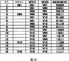
图11是表示4位DAC的输入输出特性的输入输出电平对应关系图。参照图11,对将4个输入电压A、B、C、D选择输入到输入端子T1、T2,输出4个输入电压的平方个的16个电压电平的DAC进行说明。4个输入电压A、B、C、D向输入端子T1、T2的16种输入选择,由4位数据D3、D2、D1、D0来控制。而且,图11的电平编号可以对应于图10的电压电平(Vo1~Vo16)。另外,放大电路13也能输出将输入到端子T1、T2的电压V(T1)、V(T2)内分为1对2的内插(内分)电压,使16个输出电压等间隔。FIG. 11 is a graph showing the input-output level correspondence relationship of the input-output characteristics of a 4-bit DAC. Referring to FIG. 11 , a DAC that selectively inputs four input voltages A, B, C, and D to input terminals T1 and T2 and outputs 16 voltage levels that are squares of the four input voltages will be described. 16 input options from 4 input voltages A, B, C, D to input terminals T1, T2 are controlled by 4-bit data D3, D2, D1, D0. Also, the level numbers of FIG. 11 may correspond to the voltage levels (Vo1˜Vo16) of FIG. 10 . In addition, the amplifying
而且,将第1乃至第4参考电压A、B、C、D分别设定为第1、第4、第13、第16电平,选择电路12根据4位的选择信号D3、D2、D1、D0,可以将:Moreover, the first to fourth reference voltages A, B, C, and D are respectively set to the first, fourth, thirteenth, and sixteenth levels, and the
(01)第1、第1参考电压(A、A)、(01) 1st, 1st reference voltage (A, A),
(02)第1、第2参考电压(A、B)、(02) The first and second reference voltages (A, B),
(03)第2、第1参考电压(B、A)、(03) 2nd, 1st reference voltage (B, A),
(04)第2、第2参考电压(B、B)、(04) 2nd, 2nd reference voltage (B, B),
(05)第1、第3参考电压(A、C)、(05) The first and third reference voltages (A, C),
(06)第1、第4参考电压(A、D)、(06) The first and fourth reference voltages (A, D),
(07)第2、第3参考电压(B、C)、(07) The second and third reference voltages (B, C),
(08)第2、第4参考电压(B、D)、(08) The second and fourth reference voltages (B, D),
(09)第3、第1参考电压(C、A)、(09) 3rd, 1st reference voltage (C, A),
(10)第3、第2参考电压(C、B)、(10) The third and second reference voltages (C, B),
(11)第4、第1参考电压(D、A)、(11) 4th, 1st reference voltage (D, A),
(12)第4、第2参考电压(D、B)、(12) The 4th and 2nd reference voltages (D, B),
(13)第3、第3参考电压(C、C)、(13) The third and third reference voltages (C, C),
(14)第3、第4参考电压(C、D)、(14) The third and fourth reference voltages (C, D),
(15)第4、第3参考电压(D、C)、(15) The 4th and 3rd reference voltages (D, C),
(16)第4、第4参考电压(D、D)(16) The 4th, 4th reference voltage (D, D)
对的任一个供给到放大电路13的第1、第2端子T1、T2。并且,在放大电路13的内分比为1∶2时,第1端子电压V(T1)的2倍与第2端子电压V(T2)之和等于输出电压Vout的3倍,能够输出第1乃至第16电压电平。Either one of the pairs is supplied to the first and second terminals T1 and T2 of the
还有,在放大电路13的内分比为2∶1时,通过将端子T1与T2的输入电压设定为与上述相反,从而可以得到完全相同的输出。此时,第1端子电压V(T1)与第2端子电压V(T2)的2倍之和等于输出电压Vout的3倍,能够输出第1乃至第16电压电平。In addition, when the internal division ratio of the
图12是表示实现图11所例示的控制的4位译码器(Nch)的构成的一例的图。参照图12,在该译码器中,是分为高位2位(D3、D2)和低位2位(D1、D0),将低位2位相对于高位2位共有化并削减了晶体管数的构成。在图12所示的例子中,可以由4个输入电压与12个晶体管401~412来构成(在图32的构成中为4个输入电压与16个晶体管401~416)。而且,各位信号D3、D2、D1、D0及其反相信号的顺序可以是任意的。FIG. 12 is a diagram illustrating an example of a configuration of a 4-bit decoder (Nch) for realizing the control illustrated in FIG. 11 . Referring to FIG. 12, this decoder is divided into upper 2 bits (D3, D2) and lower 2 bits (D1, D0), and the lower 2 bits are shared with the upper 2 bits to reduce the number of transistors. In the example shown in FIG. 12 , it can be configured with four input voltages and 12 transistors 401 to 412 (in the configuration of FIG. 32 , four input voltages and 16 transistors 401 to 416 ). Furthermore, the order of the bit signals D3, D2, D1, D0 and their inverted signals may be arbitrary.
参照图12,该译码器电路(选择电路)备有:With reference to Fig. 12, this decoder circuit (selection circuit) has:
连接在第1参考电压(A:电平1)与所述第1端子T1之间,并将D1B与D3B分别输入到控制端子的第1及第2开关401、402;connected between the first reference voltage (A: level 1) and the first terminal T1, and input D1B and D3B to the first and second switches 401 and 402 of the control terminals respectively;
连接在第1参考电压A与第2端子T2之间,并将D0B与D2B分别输入到控制端子的第3及第4开关403、404;connected between the first reference voltage A and the second terminal T2, and input D0B and D2B to the third and fourth switches 403 and 404 of the control terminals respectively;
连接在第2参考电压(B:电平4)与第1端子T1之间,并将D1与D3B分别输入到控制端子的第5及第6开关405、406;connected between the second reference voltage (B: level 4) and the first terminal T1, and input D1 and D3B to the fifth and sixth switches 405 and 406 of the control terminals respectively;
连接在第2参考电压B与第2端子T2之间,并将D0与D2B分别输入到控制端子的第7及第8开关407、408;connected between the second reference voltage B and the second terminal T2, and input D0 and D2B to the seventh and eighth switches 407 and 408 of the control terminals respectively;
连接在第3参考电压(C:电平13)与第1及第2开关401、402的连接点之间,并将D3输入到控制端子的第9开关409;Connected between the third reference voltage (C: level 13) and the connection point of the first and second switches 401, 402, and input D3 to the ninth switch 409 of the control terminal;
连接在第3参考电压C与第3及第4开关403、404的连接点之间,并将D2输入到控制端子的第10开关410;connected between the third reference voltage C and the connection points of the third and fourth switches 403, 404, and input D2 to the tenth switch 410 of the control terminal;
连接在第4参考电压(D:电平16)与第5及第6开关405、406的连接点之间,并将D3输入到控制端子的第11开关411;Connected between the fourth reference voltage (D: level 16) and the connection point of the fifth and sixth switches 405, 406, and input D3 to the eleventh switch 411 of the control terminal;
连接在第4参考电压D与所述第7及第8开关407、408的连接点之间,并将D2输入到控制端子的第12开关412。即,晶体管的数为401~412的共计12个。The twelfth switch 412 is connected between the fourth reference voltage D and the connection point of the seventh and eighth switches 407 and 408 and inputs D2 to the control terminal. That is, the number of transistors is 12 in total of 401 to 412 .
图13是表示图12的另一变形例的图,是分为高位2位(D3、D2)与低位2位(D1、D0),将高位2位相对于低位2位共有化来削减晶体管数的构成。参照图13,备有:Fig. 13 is a diagram showing another modified example of Fig. 12, which is divided into upper 2 bits (D3, D2) and lower 2 bits (D1, D0), and the upper 2 bits are shared with the lower 2 bits to reduce the number of transistors constitute. Referring to Figure 13, there are:
连接在第1参考电压A(电平V1)与第1端子T1之间,并将D1B与D3B分别输入到控制端子的第1及第2开关401、402;connected between the first reference voltage A (level V1) and the first terminal T1, and input D1B and D3B to the first and second switches 401 and 402 of the control terminals respectively;
连接在第1参考电压A与第2端子T2之间,并将D0B与D2B分别输入到控制端子的第3及第4开关403、404;connected between the first reference voltage A and the second terminal T2, and input D0B and D2B to the third and fourth switches 403 and 404 of the control terminals respectively;
连接在第2参考电压B(电平V4)与所述第1及第2开关401、402的连接点之间,并将D1输入到控制端子的第5开关405;Connected between the second reference voltage B (level V4) and the connection point of the first and second switches 401, 402, and input D1 to the fifth switch 405 of the control terminal;
连接在第2参考电压B与所述第3及第4开关403、404的连接点之间,并将D0输入到控制端子的第6开关406;connected between the second reference voltage B and the connection point of the third and fourth switches 403, 404, and input D0 to the sixth switch 406 of the control terminal;
连接在第3参考电压C(电平V13)与第1端子T1之间,并将D1B与D3分别输入到控制端子的第7及第8开关407、408;Connected between the third reference voltage C (level V13) and the first terminal T1, and input D1B and D3 to the seventh and eighth switches 407 and 408 of the control terminals respectively;
连接在第3参考电压C与第2端子T2之间,并将D0B与D2分别输入到控制端子的第9及第10开关409、410;connected between the third reference voltage C and the second terminal T2, and input D0B and D2 to the ninth and tenth switches 409 and 410 of the control terminals respectively;
连接在第4参考电压D(电平V16)与第7及第8开关407、408的连接点之间,并将D1输入到控制端子的第11开关411;Connected between the fourth reference voltage D (level V16) and the connection point of the seventh and eighth switches 407, 408, and input D1 to the eleventh switch 411 of the control terminal;
连接在第4参考电压D与所述第9及第10开关409、410的连接点之间,并将D0输入到控制端子的第12开关412。该情况下晶体管数也为12个。The twelfth switch 412 is connected between the fourth reference voltage D and the connection point of the ninth and tenth switches 409 and 410 and inputs D0 to the control terminal. In this case, the number of transistors is also twelve.
这样,作为译码器的电路构成,各种各样的构成是可能的,由于其构成不同,晶体管数也稍有不同。但是,无论何种构成,都成为:经由将D1B与D3B分别输入到控制端子的2个开关连接第1参考电压A与第1端子T1之间;经由将D0B与D2B分别输入到控制端子的2个开关连接第1参考电压A与第2端子T2之间;Thus, various configurations are possible as a circuit configuration of the decoder, and the number of transistors is slightly different depending on the configuration. However, regardless of the configuration, the first reference voltage A is connected to the first terminal T1 via two switches that respectively input D1B and D3B to the control terminals; A switch is connected between the first reference voltage A and the second terminal T2;
经由将D1与D3B分别输入到控制端子的2个开关连接第2参考电压B与第1端子T1之间;Connect between the second reference voltage B and the first terminal T1 via two switches that respectively input D1 and D3B to the control terminals;
经由将D0与D2B分别输入到控制端子的2个开关连接第2参考电压B与第2端子T2之间;Connect between the second reference voltage B and the second terminal T2 via two switches that respectively input D0 and D2B to the control terminal;
经由将D1B与D3分别输入到控制端子的2个开关连接第3参考电压C与第1端子T1之间;Connect between the third reference voltage C and the first terminal T1 via two switches that respectively input D1B and D3 to the control terminals;
经由将D0B与D2分别输入到控制端子的2个开关连接第3参考电压C与第2端子T2之间;Connect between the third reference voltage C and the second terminal T2 via two switches that respectively input D0B and D2 to the control terminals;
经由将D1与D3分别输入到控制端子的2个开关连接第4参考电压D与第1端子T1之间;Connect between the fourth reference voltage D and the first terminal T1 via two switches that respectively input D1 and D3 to the control terminals;
经由将D0与D2分别输入到控制端子的2个开关连接第4参考电压D与第2端子T2之间的构成。在以下的译码器的说明中,以晶体管数较少的代表性构成为例进行说明。而且,与参照图12、图13说明的4位译码器的变形例同样,即使在以下所说明的本发明的多位译码器的代表性构成中,也可以成为与经由将选择用信号输入到控制端子的多个开关来连接规定的参考电压与规定的端子(T1或T2)的构成相同的变形例。A configuration in which the fourth reference voltage D and the second terminal T2 are connected via two switches for inputting D0 and D2 to the control terminals, respectively. In the following description of the decoder, a typical configuration with a small number of transistors will be described as an example. 12 and 13, even in the representative configuration of the multi-bit decoder of the present invention described below, it is also possible to use the selection signal via the A modification in which a predetermined reference voltage is connected to a plurality of switches inputted to a control terminal and a predetermined terminal (T1 or T2) has the same configuration.
在相同的4位译码器中,如果与图24所示的现有的译码器(图21的译码器984的具体例)相比,则图12、图13不仅可以削减输入电压数(参考电压的个数),构成译码器电路的晶体管数也在相对于图24的30个而在图12、图13所示的构成中仅有12个的状况,被大幅度削减,可以实现节省面积化。In the same 4-bit decoder, if compared with the conventional decoder shown in FIG. 24 (a specific example of the decoder 984 in FIG. 21 ), not only can the number of input voltages be reduced in FIGS. 12 and 13 (Number of reference voltages), the number of transistors constituting the decoder circuit is also reduced to 12 in the configuration shown in FIG. 12 and FIG. 13 compared to 30 in FIG. Realize area saving.
即使对于4位以上的数据输入的译码器,同样也可以说节省面积的效果高。因此,通过采用本发明,从而可以大幅度简化译码器并能进行节省面积化。Similarly, it can be said that the area saving effect is high even for a decoder for inputting data of 4 bits or more. Therefore, by adopting the present invention, it is possible to greatly simplify the decoder and realize area saving.
图14是表示:在图1的数字模拟转换器(DAC)中,作为选择电路12采用图12、图13所示的译码器电路,作为放大电路13采用图5所示的差动放大器的4位DAC的输出波形的图。图14是:在一定期间内使4位数据D3、D2、D1、D0顺次变化为(0,0,0,0)→(0,0,0,1)→(0,0,1,0)→…→(1,1,1,1)时的端子T1、T2的电压V(T1)、V(T2)及DAC输出电压Vout的输出波形。输入电压A、B、C、D分别设为5.00V、5.06V、5.24V、5.30V,输出电压Vout的相邻电平间的电压差设定为20mV。通过图14可以确认:根据从(0,0,0,0)到(1,1,1,1)为止的4位数据,可以高精度地输出从5.0V到5.3V为止、20mV间隔的16个电平。FIG. 14 shows: in the digital-to-analog converter (DAC) of FIG. 1, the decoder circuit shown in FIG. 12 and FIG. 13 is used as the
接下来,作为本发明的其他实施例,对6位DAC的构成进行说明。图15是表示本实施例的6位DAC的输入输出特性的输入输出电平对应关系的图。在该例中,就向输入端子T1、T2选择输入8个输入电压A、B、C、D、E、F、G、H中的2个(包含相同电压的情况),输出8个输入电压的平方个的64个电压电平的DAC进行说明。8个输入电压A、B、C、D、E、F、G、H向输入端子T1、T2的64种输入选择,由6位数据D5、D4、D3、D2、D1、D0来控制。而且,在放大电路13可以输出将输入到端子T1、T2的电压V(T1)、V(T2)内分为1对2的内插(内分)电压时,可以使64个输出电压等间隔。另外,此时输入电压A、B、C、D、E、F、G、H设定为第1、第4、第13、第16及第49、第52、第61、第64电压电平。并且,在放大电路13输出将输入到端子T1、T2的电压V(T1)、V(T2)内分为2对1的电压的构成中,在图15中调换T1与T2。Next, a configuration of a 6-bit DAC will be described as another embodiment of the present invention. FIG. 15 is a diagram showing the input/output level correspondence relationship of the input/output characteristics of the 6-bit DAC of this embodiment. In this example, 2 of 8 input voltages A, B, C, D, E, F, G, and H (including the case of the same voltage) are selected and input to the input terminals T1 and T2, and 8 input voltages are output. The square of the 64 voltage level DAC is described. 8 input voltages A, B, C, D, E, F, G, H to input terminals T1, T2 for 64 input options, controlled by 6-bit data D5, D4, D3, D2, D1, D0. Furthermore, when the amplifying
若将8个参考电压A~H分别设为第01、第04、第13、第16、第49、第52、第61、第64电平(V1、V4、V13、V16、V49、V52、V61、V64),则选择电路(译码器电路)12根据6位的数据信号(选择信号),可以向放大电路13的第1、第2端子T1、T2供给:If the eight reference voltages A~H are respectively set to the 01st, 04th, 13th, 16th, 49th, 52nd, 61st, and 64th levels (V1, V4, V13, V16, V49, V52, V61, V64), then the selection circuit (decoder circuit) 12 can supply to the first and second terminals T1, T2 of the
(01)第1、第1参考电压(A、A)、(01) 1st, 1st reference voltage (A, A),
(02)第1、第2参考电压(A、B)、(02) The first and second reference voltages (A, B),
(03)第2、第1参考电压(B、A)、(03) 2nd, 1st reference voltage (B, A),
(04)第2、第2参考电压(B、B)、(04) 2nd, 2nd reference voltage (B, B),
(05)第1、第3参考电压(A、C)、(05) The first and third reference voltages (A, C),
(06)第1、第4参考电压(A、D)、(06) The first and fourth reference voltages (A, D),
(07)第2、第3参考电压(B、C)、(07) The second and third reference voltages (B, C),
(08)第2、第4参考电压(B、D)、(08) The second and fourth reference voltages (B, D),
(09)第3、第1参考电压(C、A)、(09) 3rd, 1st reference voltage (C, A),
(10)第3、第2参考电压(C、B)、(10) The third and second reference voltages (C, B),
(11)第4、第1参考电压(D、A)、(11) 4th, 1st reference voltage (D, A),
(12)第4、第2参考电压(D、B)、(12) The 4th and 2nd reference voltages (D, B),
(13)第3、第3参考电压(C、C)、(13) The third and third reference voltages (C, C),
(14)第3、第4参考电压(C、D)、(14) The third and fourth reference voltages (C, D),
(15)第4、第3参考电压(D、C)、(15) The 4th and 3rd reference voltages (D, C),
(16)第4、第4参考电压(D、D)、(16) The 4th and 4th reference voltages (D, D),
(17)第1、第5参考电压(A、E)、(17) The first and fifth reference voltages (A, E),
(18)第1、第6参考电压(A、F)、(18) The first and sixth reference voltages (A, F),
(19)第2、第5参考电压(B、E)、(19) The second and fifth reference voltages (B, E),
(20)第2、第6参考电压(B、F)、(20) The second and sixth reference voltages (B, F),
(21)第1、第7参考电压(A、G)、(21) The first and seventh reference voltages (A, G),
(22)第1、第8参考电压(A、H)、(22) The first and eighth reference voltages (A, H),
(23)第2、第7参考电压(B、G)、(23) The second and seventh reference voltages (B, G),
(24)第2、第8参考电压(B、H)、(24) The second and eighth reference voltages (B, H),
(25)第3、第5参考电压(C、E)、(25) The third and fifth reference voltages (C, E),
(26)第3、第6参考电压(C、F)、(26) The third and sixth reference voltages (C, F),
(27)第4、第5参考电压(D、E)、(27) The 4th and 5th reference voltages (D, E),
(28)第4、第6参考电压(D、F)、(28) The 4th and 6th reference voltages (D, F),
(29)第3、第7参考电压(C、G)、(29) The 3rd and 7th reference voltages (C, G),
(30)第3、第8参考电压(C、H)、(30) The third and eighth reference voltages (C, H),
(31)第4、第7参考电压(D、G)、(31) The 4th and 7th reference voltages (D, G),
(32)第4、第8参考电压(D、H)、(32) The 4th and 8th reference voltages (D, H),
(33)第5、第1参考电压(E、A)、(33) 5th, 1st reference voltage (E, A),
(34)第5、第2参考电压(E、B)、(34) The fifth and second reference voltages (E, B),
(35)第6、第1参考电压(F、A)、(35) 6th, 1st reference voltage (F, A),
(36)第6、第2参考电压(F、B)、(36) The sixth and second reference voltages (F, B),
(37)第5、第3参考电压(E、C)、(37) The fifth and third reference voltages (E, C),
(38)第5、第4参考电压(E、D)、(38) The fifth and fourth reference voltages (E, D),
(39)第6、第3参考电压(F、C)、(39) The sixth and third reference voltages (F, C),
(40)第6、第4参考电压(F、D)、(40) The sixth and fourth reference voltages (F, D),
(41)第7、第1参考电压(G、A)、(41) 7th, 1st reference voltage (G, A),
(42)第7、第2参考电压(G、B)、(42) The seventh and second reference voltages (G, B),
(43)第8、第1参考电压(H、A)、(43) 8th, 1st reference voltage (H, A),
(44)第8、第2参考电压(H、B)、(44) 8th, 2nd reference voltage (H, B),
(45)第7、第3参考电压(G、C)、(45) The seventh and third reference voltages (G, C),
(46)第7、第4参考电压(G、D)、(46) The seventh and fourth reference voltages (G, D),
(47)第8、第3参考电压(H、C)、(47) The 8th and 3rd reference voltages (H, C),
(48)第8、第4参考电压(H、D)、(48) The 8th and 4th reference voltages (H, D),
(49)第5、第5参考电压(E、E)、(49) 5th, 5th reference voltage (E, E),
(50)第5、第6参考电压(E、F)、(50) The fifth and sixth reference voltages (E, F),
(51)第6、第5参考电压(F、E)、(51) The sixth and fifth reference voltages (F, E),
(52)第6、第6参考电压(F、F)、(52) The sixth and sixth reference voltages (F, F),
(53)第5、第7参考电压(E、G)、(53) The fifth and seventh reference voltages (E, G),
(54)第5、第8参考电压(E、H)、(54) The fifth and eighth reference voltages (E, H),
(55)第6、第7参考电压(F、G)、(55) The sixth and seventh reference voltages (F, G),
(56)第6、第8参考电压(F、H)、(56) The sixth and eighth reference voltages (F, H),
(57)第7、第5参考电压(G、E)、(57) The seventh and fifth reference voltages (G, E),
(58)第7、第6参考电压(G、F)、(58) The seventh and sixth reference voltages (G, F),
(59)第8、第5参考电压(H、E)、(59) The 8th and 5th reference voltages (H, E),
(60)第8、第6参考电压(H、F)、(60) The 8th and 6th reference voltages (H, F),
(61)第7、第7参考电压(G、G)、(61) The seventh and seventh reference voltages (G, G),
(62)第7、第8参考电压(G、H)、(62) The seventh and eighth reference voltages (G, H),
(63)第8、第7参考电压(H、G)、(63) The 8th and 7th reference voltages (H, G),
(64)第8、第8参考电压(H、H)的对的任一个。而且,放大电路13的内分比为1∶2时,第1端子电压V(T1)的2倍与第2端子电压V(T2)之和等于输出电压Vout的3倍,能够输出第1乃至第64电压电平。并且,在放大电路13的内分比为2∶1时,通过将图15的T1与T2的输入电压设定为与上述相反,从而可以得到完全相同的输出。此时,第1端子电压V(T1)与第2端子电压V(T2)的2倍之和等于输出电压Vout的3倍,能够输出第1乃至第64电压电平。(64) Either one of the eighth, eighth reference voltage (H, H) pair. Moreover, when the internal division ratio of the amplifying
图16是可以实现图15的控制的6位译码器(Nch)的构成例。图16是按每2位分为(D5,D4)、(D3,D2)、(D1,D0),将高位位相对于低位位共有化而削减晶体管数的构成。Fig. 16 is a configuration example of a 6-bit decoder (Nch) capable of realizing the control in Fig. 15 . FIG. 16 is a configuration in which each 2 bits is divided into (D5, D4), (D3, D2), and (D1, D0), and the upper bits are shared with the lower bits to reduce the number of transistors.
参照图16,该译码器电路备有:Referring to Figure 16, the decoder circuit is provided with:
连接在第1参考电压A(V1)与第1端子T1之间,并将D1B、D3B与D5B分别输入到控制端子的第1乃至第3开关501~503;Connected between the first reference voltage A (V1) and the first terminal T1, and input D1B, D3B and D5B to the first and third switches 501-503 of the control terminals respectively;
连接在第1参考电压A与第2端子T2之间,并将D0B、D2B与D4B分别输入到控制端子的第4乃至第6开关504~506;Connected between the first reference voltage A and the second terminal T2, and input D0B, D2B and D4B to the fourth and sixth switches 504-506 of the control terminals respectively;
连接在第2参考电压B(V4)与第1及第2开关501、502的连接点之间,并将D1输入到控制端子的第7开关507;Connected between the second reference voltage B (V4) and the connection point of the first and second switches 501 and 502, and input D1 to the seventh switch 507 of the control terminal;
连接在第2参考电压B与所述第4及第5开关504、505的连接点之间,并将D0输入到控制端子的第8开关508;connected between the second reference voltage B and the connection points of the fourth and fifth switches 504, 505, and input D0 to the eighth switch 508 of the control terminal;
连接在第3参考电压C(V13)与第2及第3开关502、503的连接点之间,并将D1B与D3分别输入到控制端子的第9及第10开关509、510;Connected between the third reference voltage C (V13) and the connection points of the second and third switches 502, 503, and input D1B and D3 to the ninth and tenth switches 509, 510 of the control terminals respectively;
连接在第3参考电压C与第5及第6开关505、506的连接点之间,并将D0B与D2分别输入到控制端子的第11及第12开关511、512;connected between the third reference voltage C and the connection points of the fifth and sixth switches 505, 506, and input D0B and D2 to the eleventh and twelfth switches 511, 512 of the control terminals respectively;
连接在第4参考电压D(V16)与第9及第10开关509、510的连接点之间,并将D1输入到控制端子的第13开关513;connected between the fourth reference voltage D (V16) and the connection points of the ninth and tenth switches 509, 510, and input D1 to the thirteenth switch 513 of the control terminal;
连接在第4参考电压D与第11及第12开关511、512的连接点之间,并将D0输入到控制端子的第14开关514;A 14th switch 514 connected between the 4th reference voltage D and the connection points of the 11th and 12th switches 511, 512, and inputting D0 to the control terminal;
连接在第5参考电压E(V49)与第1端子T1之间,并将D1B、D3B与D5分别输入到控制端子的第15乃至第17开关515~517;Connect between the fifth reference voltage E (V49) and the first terminal T1, and input D1B, D3B and D5 to the fifteenth and seventeenth switches 515-517 of the control terminals respectively;
连接在第5参考电压E与第2端子T2之间,并将D0B、D2B与D4分别输入到控制端子的第18乃至第20开关518~520;connected between the fifth reference voltage E and the second terminal T2, and input D0B, D2B and D4 to the eighteenth and even the twentyth switches 518-520 of the control terminals respectively;
连接在第6参考电压F(V52)与第15及第16开关515、516的连接点之间,并将D1输入到控制端子的第21开关521;The 21st switch 521 connected between the 6th reference voltage F(V52) and the connection points of the 15th and 16th switches 515, 516, and inputting D1 to the control terminal;
连接在第6参考电压F与第18及第19开关518、519的连接点之间,并将D0输入到控制端子的第22开关522;The 22nd switch 522 connected between the 6th reference voltage F and the connection points of the 18th and 19th switches 518, 519, and inputting D0 to the control terminal;
连接在第7参考电压G(V61)与第16及第17开关516、517的连接点之间,并将D1B与D3分别输入到控制端子的第23及第24开关523、524;connected between the 7th reference voltage G (V61) and the connection points of the 16th and 17th switches 516, 517, and input D1B and D3 to the 23rd and 24th switches 523, 524 of the control terminals respectively;
连接在第7参考电压G与第19及第20开关519、520的连接点之间,并将D0B与D2分别输入到控制端子的第25及第26开关525、526;connected between the 7th reference voltage G and the connection points of the 19th and 20th switches 519, 520, and input D0B and D2 to the control terminals of the 25th and
连接在第8参考电压H(V64)与第23及第24开关523、524的连接点之间,并将D1输入到控制端子的第27开关527;The 27th switch 527 connected between the 8th reference voltage H (V64) and the connection points of the 23rd and 24th switches 523 and 524, and inputting D1 to the control terminal;
连接在第8参考电压H与第25及第26开关525、526的连接点之间,并将D0输入到控制端子的第28开关528。图16所示的构成可以由8个输入电压A~H(V1、V4、V13、V16、V49、V52、V61、V64)和28个晶体管501~528来构成。因此,如果利用本发明,则可以大幅度简化译码器,能够节省面积。而且,各位信号D5、D4、D3、D2、D1、D0及其反相信号的顺序是任意的。另外,经由将规定的信号输入到控制端子的多个开关来连接规定的参考电压与规定的端子(T1或T2)的构成,如果与图16相同,则能够进行任意的变更。The 28th switch 528 is connected between the eighth reference voltage H and the connection point of the 25th and
图17是表示:在图1的数字模拟转换器(DAC)中,作为选择电路12采用图16所示的译码器电路、作为图1的放大电路13采用图5的差动放大器的6位DAC的输出波形的图。在图17中示出:在一定期间内使6位数据D5、D4、D3、D2、D1、D0顺次变化为例如(0,0,0,0,0,0)→(0,0,0,0,0,1)→(0,0,0,0,1,0)→…→(1,1,1,1,1,1)时的端子T1、T2的电压V(T1)、V(T2)及DAC输出电压Vout的输出电压波形。输入电压A、B、C、D、E、F、G、H分别设为5.00V、5.01V、5.04V、5.05V、5.16V、5.17V、5.20V、5.21V,输出电压Vout的相邻电平间的电压差设定为3.3mV。通过图17可以确认:根据6位数据,可以高精度地输出从5.01V到5.21V为止、3.3mV间隔的64个电平。Fig. 17 shows: in the digital-to-analog converter (DAC) of Fig. 1, the decoder circuit shown in Fig. 16 is adopted as the
以上,对在2、4、6位的数据输入的DAC中,输出输入电压数的平方个电压电平的情况进行了说明。而且,虽然输入电压数m可以是任意的,但在输出等间隔的电压电平的情况下,输入电压数优选设定为m=2、4、8等2的幂乘个(m=2的K次方,其中K为1以上的整数)。该情况下,用2K位的数字数据来选择输入电压数(2K个)的平方个(=4K个)的连续的输出电平(第1~4K电平),另外各输入电压设定为下式(1)给出的顺序的电平。In the above, the case where the DAC with 2, 4, and 6-bit data input outputs a voltage level equal to the square of the input voltage has been described. Moreover, although the number m of input voltages can be arbitrary, in the case of outputting voltage levels at equal intervals, the number of input voltages is preferably set to a power of 2 such as m=2, 4, 8 (m=2 K power, wherein K is an integer greater than 1). In this case, 2K-bit digital data is used to select continuous output levels (1st to4K levels) of the square (=4K ) of the number of input voltages (2K ), and each input voltage setting Set to levels in the order given by the following equation (1).
{1+a1×4(K-1)+a2×4(K-2)+a3×4(K-3)+…+aK×4(K-K)}{1+a1×4(K-1) +a2×4(K-2) +a3×4(K-3) +…+aK×4(KK) }
…(1) …(1)
其中,在上式(1)中,系数a1、a2、a3、…取0或3。Wherein, in the above formula (1), the coefficients a1, a2, a3, . . . take 0 or 3.
例如,在K=1时,输入电压数m为m=2,2个输入电压为连续的4个输出电平(1电平~4电平)中、(1+a1)电平(a1=0,3)。即,如图7所示,输入电压A、B为电平1、4。For example, when K=1, the number of input voltages m is m=2, 2 input voltages are continuous 4 output levels (1 level to 4 levels), (1+a1) level (a1= 0, 3). That is, as shown in FIG. 7 , input voltages A and B are at
另外,在K=2时,输入电压数m为m=4,4个输入电压变为连续的16个输出电平中的、{1+a1×4+a2}电平(a1、a2=0,3)。即,如图11所示,4个输入电压A、B、C、D为电平1(a1=a2=0)、电平4(a1=0,a2=3)、电平13(a1=3,a2=0)、电平16(a1=a3=3)。In addition, when K=2, the number of input voltages m is m=4, and the 4 input voltages become {1+a1×4+a2} levels (a1, a2=0 , 3). That is, as shown in Figure 11, the four input voltages A, B, C, D are level 1 (a1=a2=0), level 4 (a1=0, a2=3), level 13 (a1= 3, a2=0), level 16 (a1=a3=3).
在K=3时,输入电压数m为m=8,8个输入电压变为连续的64个输出电平中的、{1+a1×4+a2×16+a3}电平(a1、a2、a3=0,3),系数的组(a1,a2,a3)=(0,0,0)、(0,0,3)、(0,3,0)、(0,3,3)、(3,0,0)、(3,0,3)、(3,3,0)、(3,3,3)所分别对应的电平1、4、13、16、49、52、61、64变为图15所示的输入电压A~H。When K=3, the number of input voltages m is m=8, and the 8 input voltages become {1+a1×4+a2×16+a3} levels (a1, a2 , a3=0, 3), the group of coefficients (a1, a2, a3)=(0, 0, 0), (0, 0, 3), (0, 3, 0), (0, 3, 3) , (3, 0, 0), (3, 0, 3), (3, 3, 0), (3, 3, 3) corresponding to the
即,与2、4、6的2K位的数据输入的DAC(图7、图11、图15)各自的输入电压的设定一致。这对于K=4以上也同样成立。That is, it corresponds to the setting of each input voltage of the DAC ( FIG. 7 , FIG. 11 , and FIG. 15 ) for 2K-bit data input of 2, 4, and 6 data. The same holds true for K=4 or more.
而且,即使为2的幂乘个以外的输入电压数,也能进行其平方个输出,但规则性的输出电平的设定有些困难。Furthermore, even if the number of input voltages is other than a power of 2, the square output can be performed, but it is somewhat difficult to set a regular output level.
通过组合到此为止说明的本发明,从而可以应用于液晶驱动器用DAC(数字模拟转换器)。即,液晶驱动器用DAC需要根据γ曲线(curve)来调节灰度等级电压的间隔。γ曲线在中间灰度等级几乎为直线,但如图19所示,在最高位灰度等级附近或最低位灰度等级附近倾斜度改变。因此,可以设计:在灰度等级特性为直线的中间灰度等级中采用输入电压数4(16分割)、输入电压数8(64分割)的译码器,在灰度等级特性为曲线的最高位灰度等级附近或最低位附近采用分割数少的输入电压数为2(分割数4)的译码器等组合为任意灰度等级特性曲线的译码器。By combining the present invention described so far, it can be applied to a DAC (digital-to-analog converter) for a liquid crystal driver. That is, the DAC for a liquid crystal driver needs to adjust the interval of grayscale voltages according to a γ curve. The γ curve is almost a straight line at the intermediate grayscale level, but as shown in FIG. 19 , the inclination changes near the highest grayscale level or near the lowest grayscale level. Therefore, it can be designed that a decoder with an input voltage number of 4 (divided by 16) and an input voltage number of 8 (divided by 64) is used in the intermediate gray scale with a gray scale characteristic of a straight line, and the gray scale characteristic is the highest of the curve Near the bit gray level or near the lowest bit, use a decoder with a small number of divisions and an input voltage number of 2 (division number 4), which is combined into an arbitrary gray level characteristic curve.
图18是对液晶用途等显示装置的数据驱动器适用本发明的构成。参照图18,以上述实施例来构成译码器12与放大电路(放大器)13。锁存地址选择器、锁存器等电路块与图21同样。在图18所示的构成中,通过将本发明适用于DAC整体或中间灰度等级的部分,从而即使增加分割数,也无需变更放大器的构成,由于可以大幅度削减构成此时的译码器12的晶体管数,故数据驱动器整体的节省面积化也可以实现。另外,在灰度等级电压产生电路14中,生成上述各实施例的参考电压。因此,即使在灰度等级电压产生电路14中也可以大幅度削减所生成的电压数。Fig. 18 shows a configuration in which the present invention is applied to a data driver of a display device such as a liquid crystal application. Referring to FIG. 18, the
而且,灰度等级电压产生电路14可以设为将其一部分或全部设置在数据驱动器的外部的构成。另外,在将本发明应用于DAC的情况下,希望输入到1个区间的多个参考电压相对于灰度等级值尽量设定为线性。以下对该理由进行说明。例如在图11所示的情况下,即在参考电压数为4个、输出16电平的区间中,由于16个输出电压电平通过参考电压的运算来生成,故在相对于灰度等级值而将参考电压设定为线性的情况下,16个输出电平全部为线性。另一方面,在参考电压没有被设定为线性的情况下,不仅16个输出电平没有变为线性,而且根据情况的不同,成为灰度等级翻转的原因。这对于显示装置的驱动电路来说是致命的。由此,希望参考电压相对于灰度等级值设定为线性。此外,在液晶数据驱动器等根据γ曲线来进行调整的情况下,希望灰度等级电压产生电路14调整区间两端的电平所对应的灰度等级电压。若将区间的中间电平所对应的电压设为调整点,则输入到该区间的参考电压未被设定为线性,因此产生上述问题。In addition, the gradation
以上,虽然对本发明涉及的差动放大器及使用其的DAC的实施例进行了说明,但本发明涉及的差动放大器及DAC不止是形成于硅基板上的LSI电路,也能是置换为形成于玻璃或塑料等绝缘性基板上的没有背面栅极(back gate)的薄膜晶体管的构成。As mentioned above, although the examples of the differential amplifier and the DAC using the same according to the present invention have been described, the differential amplifier and the DAC according to the present invention are not limited to an LSI circuit formed on a silicon substrate, but can also be formed on a A thin film transistor without a back gate on an insulating substrate such as glass or plastic.
再者,采用了本发明涉及的差动放大器及DAC的数据驱动器,可以用作图20所示的液晶显示装置的数据驱动器980。具备本发明涉及的差动放大器及DAC的数据驱动器980通过减小译码器面积,从而低成本化成为可能,使用其的液晶显示装置的低成本化也可以实现。而且,图20所示的液晶显示装置也可以构成为,将数据驱动器980作为硅LSI单独地形成后连接在显示部960上,或者也可以采用多晶硅TFT(薄膜晶体管)等,通过形成电路而在玻璃基板等绝缘性基板上与显示部960一体地形成。特别是,在将数据驱动器与显示部一体地形成的情况下,根据本发明,通过减小数据驱动器的面积,从而窄框化(缩短显示部960的外周与基板外周的宽度)也成为可能。Furthermore, a data driver using the differential amplifier and DAC according to the present invention can be used as the data driver 980 of the liquid crystal display device shown in FIG. 20 . The data driver 980 including the differential amplifier and DAC according to the present invention can reduce the cost by reducing the area of the decoder, and the cost of the liquid crystal display device using it can also be reduced. Furthermore, the liquid crystal display device shown in FIG. 20 may also be configured such that the data driver 980 is formed separately as a silicon LSI and connected to the display portion 960, or a polysilicon TFT (thin film transistor) or the like may be used, and the data driver 980 may be connected to the display unit 960 by forming a circuit. The display unit 960 is integrally formed on an insulating substrate such as a glass substrate. In particular, when the data driver is integrally formed with the display unit, according to the present invention, it is also possible to reduce the area of the data driver to narrow the frame (shortening the width of the outer periphery of the display unit 960 and the outer periphery of the substrate).
也包含其他方式,即使对于这种显示装置的数据驱动器的任一个,通过采用本发明涉及的差动放大器及DAC,从而可以促进显示装置的低成本化或窄框化。例如,与液晶显示装置同样,即使对于向数据线输出多值电平的电压信号后进行显示的有源矩阵驱动方式的有机EL显示器等显示装置,当然也可以采用本发明涉及的差动放大器。Including other aspects, even for any of the data drivers of such a display device, by using the differential amplifier and DAC according to the present invention, it is possible to promote cost reduction or frame narrowing of the display device. For example, like a liquid crystal display device, the differential amplifier according to the present invention can of course also be used for a display device such as an organic EL display of an active matrix driving method that outputs multi-level voltage signals to data lines for display.
用上述实施例说明的差动放大器由MOS晶体管构成,在液晶显示装置的驱动电路中,例如也可以由多晶硅构成的MOS晶体管(TFT)来构成。另外,在上述实施例中,虽然示出适用于集成电路的例子,但当然也可以适用于分立(discrete)元件构成。The differential amplifier described in the above-mentioned embodiments is composed of MOS transistors, but may be composed of, for example, MOS transistors (TFTs) composed of polysilicon in a drive circuit of a liquid crystal display device. In addition, in the above-mentioned embodiments, although an example applied to an integrated circuit was shown, it is of course also applicable to a discrete element configuration.
以下,对本说明书第7页第29行~第8页第13行以及第31页第26行~第32页第18行的说明进一步补充。在本发明涉及的数字模拟转换电路中,在输入电压数m为2的幂次方个(m=2K,其中K为正整数)、输出电压数为4K个的情况下,用于选择输出电压的数字数据信号最小为2K位。这是因为可以通过作为二进制的数字数据可以选择的数是用2的位数次方来规定的,即,2的2K次方为4K,从对应于上述输出电压数的情况来看也是容易理解的。而且,在上述实施例中,针对将图8、图12、图13、图16说明的数字数据信号在下面扩展为2K位(其中K为正整数)的情况,说明数字数据信号为2、4、6位时的译码器构成例。图30是表示数字数据信号为2K位的本实施例的译码器(选择电路)的构成。Hereinafter, the explanations on
参照图30,该译码器是通过2K位的数字数据信号来选择2的K次方(2K)个输入电压V(1)、V(2)、V(3)、…、V(2K),并输出到端子T1、T2的译码器构成。图30的译码器由从第1列到第K列为止的电路块组构成,各电路块组由单个或多个电路块61构成。电路块61构成为:在4个输入端子I1~I4接收电压信号,将根据2位信号而选择出的电压信号由2个输出端子O1、O2输出。Referring to Fig. 30, the decoder selects 2 to the Kth power (2K ) input voltages V(1), V(2), V(3), ..., V(2) through a 2K-bit digital data signalK ), and output to the decoder of terminals T1 and T2. The decoder in FIG. 30 is composed of circuit block groups from the first column to the Kth column, and each circuit block group is composed of a single or a plurality of circuit blocks 61 . The circuit block 61 is configured to receive a voltage signal at four input terminals I1 to I4, and output a voltage signal selected from a 2-bit signal through two output terminals O1 and O2.
第1列电路块组由2的(K-1)次方个电路块61构成。此时,各电路块61分别与4个输入端子的I1与I2及I3与I4共同连接,向其2个输入端输入第1乃至第2K参考电压(V(1)~V(2K))的各2个。而且,在各电路块61中,所输入的2个参考电压根据数字数据信号的第1、第2位信号D0、D1而被选择,并作为2个输出电压信号而被输出到端子O1、O2。The circuit block group in the first column is composed of 2(K−1) power circuit blocks 61 . At this time, each circuit block 61 is connected to the four input terminals I1 and I2 and I3 and I4 respectively, and the first and secondK reference voltages (V(1)~V(2K ) are input to the two input terminals. ) of each 2. In addition, in each circuit block 61, the two input reference voltages are selected according to the first and second bit signals D0 and D1 of the digital data signal, and are output as two output voltage signals to the terminals O1 and O2. .
第2列电路块组由2的(K-2)次方个电路块61构成。此时各电路块61分别向4个输入端子I1~I4输入第1列电路块组的各2个电路块61的输出电压信号(共计4个)。并且,在各电路块61中,所输入的4个电压信号根据数字数据信号的第3、第4位信号D2、D3而被选择,并作为2个输出电压信号而被输出到端子O1、O2。The circuit block group in the second column is composed of 2(K-2) power circuit blocks 61 . At this time, each circuit block 61 inputs output voltage signals (four in total) of each of the two circuit blocks 61 of the circuit block group in the first column to the four input terminals I1 to I4, respectively. In addition, in each circuit block 61, the four input voltage signals are selected according to the third and fourth bit signals D2 and D3 of the digital data signal, and are output as two output voltage signals to the terminals O1 and O2. .
以下同样,也可以构成第3列以后的电路块组。而且,若使用变量F来说明,则第F列(F为从3到K-1的正整数)的电路块组由2的(K-F)次方个电路块61构成。此时,各电路块61分别向4个输入端子I1~I4输入第F-1列电路块组的各2个电路块61的输出电压信号(供给4个)。而且,在各电路块61中,所输入的4个电压信号根据数字数据信号的第2F-1、第2F位信号D(2F-2)、D(2F-1)而被选择,并作为2个输出电压信号而被输出到端子O1、O2。Similarly, circuit block groups in the third and subsequent columns may also be configured. In addition, when the variable F is used to describe, the circuit block group of the F-th column (F is a positive integer ranging from 3 to K−1) is composed of 2(K−F) power circuit blocks 61 . At this time, each circuit block 61 inputs the output voltage signals of each of the two circuit blocks 61 of the F-1-th column circuit block group to the four input terminals I1 to I4 (four are supplied). In addition, in each circuit block 61, the
第K列电路块组由1个电路块61构成。此时电路块61向4个输入端子I1~I4输入第K-1列电路块组的2个电路块61的输出电压信号(共计4个)。并且,在电路块61中,所输入的4个电压信号根据数字数据信号的第2K-1、第2K位信号(D(2K-2),D(2K-2))而被选择,并作为2个输出电压信号,经由端子O1、O2而被分别输出到端子T1、T2。The K-th column circuit block group is composed of one circuit block 61 . At this time, the circuit block 61 inputs the output voltage signals (four in total) of the two circuit blocks 61 of the K-1-th column circuit block group to the four input terminals I1 to I4. And, in the circuit block 61, the
特别是,在K=1的情况下,仅构成上述第1列的电路块组,由1个电路块61构成。此时,电路块61构成为:输入第1、第2参考电压V(1)、V(2),根据第1、第2位信号D0、D1进行选择,并作为2个输出电压,经由端子O1、O2而被分别输出到端子T1、T2。而且,电路块61可以采用图31的构成。In particular, when K=1, only the circuit block group in the first column described above is constituted by one circuit block 61 . At this time, the circuit block 61 is configured to input the first and second reference voltages V(1) and V(2), select them according to the first and second bit signals D0 and D1, and use them as two output voltages via the terminal O1, O2 are output to terminals T1, T2, respectively. Furthermore, the circuit block 61 may employ the configuration shown in FIG. 31 .
图31的电路块61是2位译码器(Nch晶体管)的构成例。参照图31,该译码器由以下部件构成:连接在端子I3、I1与端子O1之间,并将数据位信号DY及其反相信号DYB分别输入到控制端子的晶体管开关703、701;连接在端子I4、I2与端子O2之间,并将数据位信号DX及其反相信号DXB分别输入到控制端子的晶体管开关704、702。并且,信号DX、DY,DY设为比DX还高位的位。The circuit block 61 in FIG. 31 is a configuration example of a 2-bit decoder (Nch transistor). Referring to Fig. 31, the decoder is composed of the following components: transistor switches 703, 701 connected between the terminals I3, I1 and the terminal O1, and inputting the data bit signal DY and its inverted signal DYB to the control terminals respectively; Between the terminals I4, I2 and the terminal O2, the data bit signal DX and its inverted signal DXB are respectively input to the transistor switches 704, 702 of the control terminals. Also, the signals DX, DY, and DY are set to higher bits than DX.
在图30的译码器中,作为电路块61,通过采用图31的构成,从而在K=1时变为与图8同等的构成,在K=2的情况下变为与图14同等的构成。即,图30所示的构成是将本发明的译码器以节省元件数来实现的译码器构成的一例。In the decoder of FIG. 30, by adopting the configuration of FIG. 31 as the circuit block 61, the configuration is equivalent to that of FIG. 8 when K=1, and the configuration is equivalent to that of FIG. 14 when K=2. constitute. That is, the configuration shown in FIG. 30 is an example of a decoder configuration in which the decoder of the present invention is realized with a reduced number of components.
另外,在上述实施例中,说明了作为译码器的构成例,即使是表示图8、图12、图13、图16并具有相同功能的译码器,有时根据其构成的不同,晶体管数也不同。此外,也说明了可以分别组合多个上述所说明的输入电压数m为2、4、8等2的幂次方个且m的值相同的译码器或m的值不同的译码器的情况。特别是,若输出电压数变得非常多,则根据译码器的构成情况,晶体管数也大为不同,大大地左右译码器的面积,因此以下对输入电压数非常多时的译码器构成与晶体管数的关系进行说明。In addition, in the above-mentioned embodiment, the configuration example of the decoder was described, and even the decoders shown in FIG. 8 , FIG. 12 , FIG. 13 , and FIG. 16 have the same functions. Also different. In addition, it is also described that a plurality of decoders whose input voltage m is 2, 4, 8, etc., which are powers of 2, and whose value of m is the same, or decoders whose values of m are different, can be combined respectively. Condition. In particular, if the number of output voltages becomes very large, the number of transistors will greatly vary depending on the configuration of the decoder, which greatly affects the area of the decoder. Therefore, the following configuration of the decoder when the number of input voltages is very large The relationship with the number of transistors will be described.
图25及图26是用于说明本发明优选的2个不同译码器的构成的图,是表示图18所示的数据驱动器的灰度等级电压产生电路14及1输出份的译码器12与放大电路(放大器)13的构成的图。FIG. 25 and FIG. 26 are diagrams for explaining the configuration of two different decoders preferred in the present invention, showing the gray scale
译码器12,作为1输出份的译码器整体或其一部分,备有S个具有输入电压数m和与其对应的m2个输出电压电平的区间(m2输出区间)。将该S个区间设为译码器块12A(图25)、译码器块12B(图26)。而且,为了使说明容易,设为在S个各区间内输出电压电平没有重复。即,图25的译码器块12A的输入电压设为(m×S)个,与其对应的输出电压电平设为(m2×S)个。图26的译码器块12B的输入电压也设为(m×S)个,与其对应的输出电压电平设为(m2×S)个。The
此外,向译码器块12A输入位组L、M、N。向译码器块12B也输入位组L、M、N。Furthermore, bit groups L, M, N are input to the
位组L、M、N是从输入到译码器12的数字数据之中选择所需的位也包含重复在内而被分配的。另外,参照图25,(m×S)个输入电压由灰度等级电压产生电路14生成并输入到译码器块12A中。参照图26,(m×S)个输入电压由灰度等级电压产生电路14生成并输入到译码器块12B中。The bit groups L, M, and N are allocated by selecting required bits from among the digital data input to the
在图25、图26中,放大电路13放大将输入到端子T1、T2的电压以1对2或2对1的内分比内分了的电压后输出。放大电路13例如为图4、图5、图6所示的构成。In FIGS. 25 and 26 , the amplifying
首先,对图25的译码器块12A的构成进行说明。译码器块12A由:输入位组L的第1~第S电路块41、输入位组M的第1及第2电路块42、输入位组N的电路块43构成。在译码器块12A中,第1~第S电路块41根据位组L从每个区间内的m个输入电压之中选择也包含重复在内的2个电压。First, the configuration of the
第1电路块42将以第1~第S电路块41的每一个选择出的2个电压的一方电压(共计S个)作为输入,第2电路块42输入以第1~第S电路块41的每一个选择出的2个电压的另一方电压(共计S个),第1及第2电路块42根据位组M从S个输入电压之中分别选择某个区间的1个电压。此时,位组M成为从译码器块12A的S个区间选择上述某一个区间的位。The
电路块43输入第1及第2电路块42的每一个选择出的电压(共计2个),根据位组N选择译码器块12A的S个区间与除此以外的区间,位组N在选择S个区间时将2个输入电压分别输出到端子T1、T2。The
而且,作为电路块41,根据输入电压数,可以采用作为上述实施例说明过的图8、图12、图13、图16、图30等的构成。另外,作为电路块42,可以采用图24的淘汰晋级(tournament)型译码器等,可以根据输入电压数来最佳化。In addition, as the
图25的译码器12的构成与晶体管数的关系是:在1区间的输入电压数m大、区间数S小的时候,成为晶体管数比较少的译码器构成。这是因为:电路块41的输入电压数m越大,电路块41的元件效率(相对于现有的同等电路的元件削减率)变得越高。The relationship between the configuration of the
接着,对图26的译码器块12B的构成进行说明。译码器块12B由输入位组M的第1~第m电路块52、输入位组L的电路块51、输入位组N的电路块53构成。在译码器块12B中,第1~第m电路块52首先从S个的各区间输入区间内相同顺序的输入电压(共计S个),根据位组M,从S个输入电压之中分别选择某个区间的1个电压。此时,位组M成为选择译码器块12B的S个区间中的上述某个区间。Next, the configuration of the
电路块51输入用第1~第m的电路块52的每一个选择出的电压(共计m个),根据位组L,从m个输入电压中选择也包含重复在内的2个电压。The
进而,电路块53输入由电路块51选择出的电压(共计2个),根据位组N,选择译码器块12B的S个区间与除此以外的区间,在位组N选择S个区间时,将2个输入电压分别输入到端子T1、T2。Furthermore, the
而且,电路块51根据输入电压数m,可以采用图8、图12、图13、图16、图30等的构成。另外,电路块52可以采用图24的淘汰晋级型译码器,可以根据输入电压数来最佳化。Furthermore, the
图26的译码器12的构成与晶体管数的关系也是:在1区间的输入电压数m大且区间数S小的时候成为晶体管数比较少的译码器构成。这是因为:电路块51的输入电压数m越大,电路块51的元件效率变得越高。The relationship between the configuration and the number of transistors of the
以上,在图25及图26中对译码器块12A及12B的2个构成例进行了说明,但各构成都希望译码器块内的(m2×S)个输出电压电平为连续的输出电压电平。In the above, two configuration examplesof the decoder blocks 12A and 12B have been described in FIG. 25 and FIG. output voltage level.
如果输出电压电平在区间与区间之间变为非连续的情况下,则按每个连续的区间分开,来构成译码器块也是可以的。If the output voltage level becomes discontinuous between sections, it is also possible to configure a decoder block for each continuous section.
另外,译码器块内的各区间可以按每个区间而单独设定相邻电压电平间的电压差(在区间内为等间隔)。In addition, the voltage difference between adjacent voltage levels can be individually set for each section in the decoder block (equal intervals within the section).
此外,在图25及图26分别示出的例子中,虽然对某个m的值所对应的译码器块12A及12B的构成进行了说明,但在译码器12具有m的值不同的区间的情况下,希望按每个m的值来构成译码器块。In addition, in the examples shown in FIG. 25 and FIG. 26 , although the configurations of the decoder blocks 12A and 12B corresponding to a certain value of m have been described, the
再有,在图25的译码器块12A中,在位组N的每个位被完全包含于位组L及M中的情况下,也可以省略电路块43。这是因为在位组L及M中已经进行着译码器块间的选择。In addition, in the
还有,在图26的译码器块12B中,在译码器12整体具有多个m的值不同的译码器块的情况下,在m为最大的译码器块中,在其位组N的每一位被全部包含于位组L及M中的情况下,可以省略电路块53。Also, in the
在m为最大的译码器块以外的译码器块中无法省略电路块53的理由是:在m小的译码器块中,在省略了电路块53的情况下,在电路块51中,会发生意想不到的端子T1、T2间的短路,有产生误输出的可能性。The reason why the
接着,对图25及图26的译码器12的构成,示出具体例并更详细地进行说明。Next, the configuration of the
图27是表示本发明的实施例的DAC中的输入输出对应的图。虽然没有特别限制,但在图27所示的例子中,表示:输入8位数据(D7~D0),根据数据来输出256个电压电平的8位DAC的输入输出对应关系。电平1~256表示从本发明涉及的放大电路13输出的输出电压电平,输入电压表示在灰度等级电压产生电路14生成并输入到译码器12的电压。另外,输入电压对应于规定的输出电压电平,在对应的输出电压电平的编号前附加记号V来表示。此外,V(T1)、V(T2)表示在本实施例的译码器(选择电路)中根据8位数据(D7~D0)而分别选择输出到端子T1、T2的电压。而且,输出电压电平表示通过放大电路13以1对2的内分比对分别输出到端子T1、T2的电压V(T1)、V(T2)进行过内分的电压。并且,在该例子中,虽然放大电路13设为输出将输出到端子T1与T2的电压内分为1∶2的电压的放大电路,但在将放大电路13设为输出内分为2∶1的电压的放大电路时,如本说明书第19页第12~18行所述,为了使输出到端子T1、T2的电压相反,只要变更电路块41或电路块51即可。在以下的说明中,为了方便,将放大电路13设为输出将端子T1与T2的电压V(T1)、V(T2)内分为1∶2的电压的放大电路。Fig. 27 is a diagram showing the correspondence between input and output in the DAC according to the embodiment of the present invention. Although not particularly limited, the example shown in FIG. 27 shows the input-output correspondence relationship of an 8-bit DAC that inputs 8-bit data (D7 to D0) and outputs 256 voltage levels according to the data.
在本实施例中,将256个输出电平(灰度等级电平)由输入电压数2、输出电压电平数4的区间(4输出区间;m=2)和输入电压数4、输出电压电平数16的区间(16输出区间;m=4)两种构成。In this embodiment, the 256 output levels (gray scale levels) are divided into intervals with 2 input voltages and 4 output voltage levels (4 output intervals; m=2) and 4 input voltages and 4 output voltages. There are two types of sections with 16 levels (16 output sections; m=4).
第1~32电压电平由4输出区间×8个来构成;The 1st to 32nd voltage levels are composed of 4 output intervals × 8;
第33~224电压电平由16输出区间×12个来构成;The 33rd to 224th voltage levels are composed of 16 output intervals × 12;
第225~256电压电平由4输出区间×8个来构成。The 225th to 256th voltage levels are composed of 4 output sections×8.
输入到译码器12的输入电压,input to the input voltage of
在4输出区间中设为各区间的第1与第4电压电平;In the 4-output section, set the first and fourth voltage levels of each section;
在16输出区间中设为各区间的第1、第4、第13、第16电压电平。相对于256个输出电平,输入电压合计为80个。In the 16 output sections, the first, fourth, thirteenth, and sixteenth voltage levels of each section are set. The input voltages add up to 80 relative to the 256 output levels.
而且,在图27中,关于从第97到176在制作附图时省略了,但根据规则性是可以容易地理解的。In addition, in FIG. 27, the 97th to 176th paragraphs are omitted when making the drawing, but they can be easily understood from the regularity.
图28是根据图25来构成实现图27的输入输出对应关系的译码器12的例子。即使在图28中,也与图25同样地示出图18所示的数据驱动器的灰度等级电压产生电路14和1输出份的译码器12和放大电路13的构成。FIG. 28 is an example of configuring the
在图28中,译码器12由译码器块12A1、12A2、12A3的3个译码器块构成。In FIG. 28, the
译码器块12A1是具有第1~32电压电平所对应的4输出区间8个份的译码器块,译码器块12A2是具有第225~256电压电平所对应的4输出区间8个份的译码器块,译码器块12A3是具有第33~224电压电平所对应的16输出区间12个份的译码器块。The decoder block 12A1 is a decoder block having 8 parts of 4 output intervals corresponding to the 1st to 32nd voltage levels, and the decoder block 12A2 is a decoder block having 8 parts of 4 output intervals corresponding to the 225th to 256th voltage levels. There are 12 decoder blocks, and the decoder block 12A3 is a decoder block with 16 output intervals corresponding to the 33rd to 224th voltage levels.
而且,由于4输出区间被分为2个连续的区间(第1~32电压电平区间与第225~256电压电平区间),故按每个连续区间进行分割来构成译码器块。Furthermore, since the 4 output intervals are divided into two consecutive intervals (1st to 32nd voltage level intervals and 225th to 256th voltage level intervals), each continuous interval is divided to form a decoder block.
另外,位组L、M、N是从输入到译码器12的1输出份的8位数据信号(D7~D0)之中进行选择所需的位也包含重复在内而被分割的。并且,8位数据信号(D7~D0)的每一位都与其反相信号(D7B~D0B)成对,但在图中省略反相信号。In addition, bit groups L, M, and N are divided into bits necessary for selection from among 8-bit data signals (D7 to D0) input to one output of the
接着,对图28的各译码器块进行说明。译码器块12A1是第1~32电压电平所对应的4输出区间的8个份的译码器块,在图25的译码器块12A中,为m=2、S=8的构成。因此,译码器块12A1由第1~第8电路块41a、第1及第2电路块42a、电路块43a构成。Next, each decoder block in FIG. 28 will be described. The decoder block 12A1 is a decoder block for 8 parts of the 4 output intervals corresponding to the 1st to 32nd voltage levels, and in the
在译码器块12A1中,对于第1~第8电路块41a,向第1电路块41a输入第1~4电压电平所对应的区间的输入电压V001及V004,向第2电路块41a输入第5~8电压电平所对应的区间的输入电压V005及V008,以下到第8电路块41a都是同样的。In the decoder block 12A1, for the first to eighth circuit blocks 41a, input voltages V001 and V004 corresponding to the first to fourth voltage levels are input to the first circuit block 41a, and input to the second circuit block 41a. The input voltages V005 and V008 in the intervals corresponding to the fifth to eighth voltage levels are the same up to the eighth circuit block 41a thereafter.
并且,在各电路块41a中,根据位组L,从各区间的2个输入电压中选择输出也包含重复在内的2个电压。因此,位组L可以是2位,也可以设为8位数据中的2位数据D1、D0。而且,各电路块41a为与图7同样的输入输出对应关系,可以采用图8的构成等。In addition, in each circuit block 41a, according to the bit group L, two voltages including overlapping are selected and output from the two input voltages in each section. Therefore, the bit group L may be 2 bits, or may be 2-bit data D1, D0 in 8-bit data. Moreover, each circuit block 41a has the same input-output correspondence relation as that of FIG. 7, and the configuration of FIG. 8 or the like can be employed.
此外,对于第1及第2电路块42a,向第1电路块42a输入由第1~第8电路块42a的每一个选择出的2个电压的一方电压(共计8个),向第2电路块42a输入由第1~第8电路块41a的每一个选择出的2个电压的另一方电压(共计8个)。In addition, with regard to the first and second circuit blocks 42a, one voltage (8 voltages in total) selected from each of the first to eighth circuit blocks 42a is input to the first circuit block 42a, and the second circuit block 42a The block 42a inputs the other voltage (8 voltages in total) of the 2 voltages selected by each of the 1st - 8th circuit block 41a.
而且,在第1及第2电路块42a中,根据位组M,分别从8个输入电压中选择输出某个区间的1个电压。此时,位组M为从译码器块12A1的8个区间选择上述某个区间的位。因此,位组M可以是3位,可以设为8位数据中的3位数据(D4、D3、D2)。并且,各电路块42a可以对图24所示的淘汰晋级型的构成等进行最佳化来使用。Furthermore, in the first and second circuit blocks 42a, one voltage in a certain section is selected and output from eight input voltages according to the bit group M, respectively. At this time, the bit group M is a bit for selecting any one of the above-mentioned sections from the eight sections of the decoder block 12A1. Therefore, the bit group M may be 3 bits, and may be set as 3-bit data ( D4 , D3 , D2 ) out of 8-bit data. In addition, each circuit block 42a can be used by optimizing the configuration of the knock-out type shown in FIG. 24 .
再有,电路块43a输入由第1及第2电路块42a的每一个选择出的电压(共计2个)。而且,在电路块43a中,根据位组N,选择译码器块12A1(第1~32电压电平所对应的区间)和除此以外的译码器块,在位组N选择译码器块12A1时,2个输入电压分别被输出到端子T1、T2。In addition, the circuit block 43a inputs voltages (two voltages in total) selected for each of the first and second circuit blocks 42a. Furthermore, in the circuit block 43a, the decoder block 12A1 (the section corresponding to the 1st to 32nd voltage levels) and other decoder blocks are selected according to the bit group N, and the decoder block is selected in the bit group N. In block 12A1, two input voltages are output to terminals T1 and T2, respectively.
在本实施例中,根据图27,译码器块12A1的区间和除此以外的选择可以用D7、D6、D5的3位来选择,位组N为8位数据中的3位数据D7、D6、D5。In this embodiment, according to FIG. 27 , the section of decoder block 12A1 and other selections can be selected using 3 bits of D7, D6, and D5, and bit group N is 3-bit data D7, D6, D5.
而且,在(D7,D6,D5)=(0,0,0)时,电路块43a将2个电压分别输出到端子T1、T2,在不为(0,0,0)时不输出到端子T1、T2。Moreover, when (D7, D6, D5) = (0, 0, 0), the circuit block 43a outputs two voltages to the terminals T1 and T2, respectively, and does not output to the terminals when it is not (0, 0, 0). T1, T2.
接下来,对译码器块12A2进行说明。译码器块12A2是第225~256电压电平所对应的4输出区间的8个份的译码器块,可以成为与译码器块12A1同样的构成。Next, the decoder block 12A2 will be described. The decoder block 12A2 is a decoder block for eight of the four output intervals corresponding to the 225th to 256th voltage levels, and may have the same configuration as the decoder block 12A1.
对于所输入的位组L、M、N,也可以设为与译码器块12A1同样的分配。The input bit groups L, M, and N may also be allocated in the same manner as the decoder block 12A1.
译码器块12A2与译码器块12A1的不同点仅在于:向译码器块的输入电压和电路块43a中的位数据(D7,D6,D5)的选择内容。若具体地说明不同点,则对于输入电压,向译码器块12A2中的第1电路块41a输入第225~228电压电平所对应的区间的输入电压V225及V228,向第2电路块41a输入第229~232电压电平所对应的输入电压V229及V232,以下到第8电路块41a为止都是同样的。另外,电路块43a中的位数据(D7,D6,D5)的选择内容,根据图27,在(D7,D6,D5)=(1,1,1)时将2个输入电压分别输出到端子T1、T2,而在(1,1,1)以外时不输出到端子T1、T2。The decoder block 12A2 differs from the decoder block 12A1 only in the input voltage to the decoder block and the selection content of the bit data (D7, D6, D5) in the circuit block 43a. To describe the difference in detail, as for the input voltage, the input voltages V225 and V228 in the interval corresponding to the 225th to 228th voltage levels are input to the first circuit block 41a in the decoder block 12A2, and the input voltages V228 and V228 are input to the second circuit block 41a. The input voltages V229 and V232 corresponding to the 229th to 232nd voltage levels are input, and the same applies to the eighth circuit block 41a. In addition, the selection content of the bit data (D7, D6, D5) in the circuit block 43a, according to FIG. 27, when (D7, D6, D5) = (1, 1, 1), two input voltages are output to the terminals respectively. T1, T2, and not output to terminals T1, T2 when it is other than (1, 1, 1).
接着,对译码器块12A3进行说明。译码器块12A3是第33~224电压电平所对应的16输出区间的12个份的译码器块,在图25的译码器块12A中,为m=4、S=12的构成。Next, the decoder block 12A3 will be described. The decoder block 12A3 is a decoder block for 12 parts of the 16 output intervals corresponding to the 33rd to 224th voltage levels. In the
因此,译码器块12A3由第1~第12电路块41b、第1及第2电路块42b、电路块43b构成。Therefore, the decoder block 12A3 is composed of the first to twelfth circuit blocks 41b, the first and second circuit blocks 42b, and the circuit block 43b.
在译码器块12A3中,对于第1~第12电路块41b,向第1电路块41b输入第33~48电压电平所对应的区间的4个输入电压V033、V036、V045及V048,向第2电路块41b输入第49~64电压电平所对应的区间的4个输入电压V049、V052、V061、V064,以下同样,对第12电路块41b输入第209~224电压电平所对应的区间的4个输入电压V209、V212、V221、V224。In the decoder block 12A3, for the first to twelfth circuit blocks 41b, four input voltages V033, V036, V045, and V048 in the intervals corresponding to the 33rd to 48th voltage levels are input to the first circuit block 41b, and are supplied to the first circuit block 41b. The second circuit block 41b inputs four input voltages V049, V052, V061, and V064 corresponding to the intervals corresponding to the 49th to 64th voltage levels. Similarly, the twelfth circuit block 41b inputs the four input voltages corresponding to the 209th to 224th voltage levels. 4 input voltages V209, V212, V221, V224 in the interval.
而且,在各电路块41b中,根据位组L,从各区间的4个输入电压中选择输出也包含重复在内的2个电压。因此,位组L可以是4位,可以设为8位数据中的4位数据(D3,D2,D1,D0)。并且,各电路块41b为与图11同样的输入输出对应关系,可以采用图12、图13的构成等。Furthermore, in each circuit block 41b, according to the bit group L, two voltages including overlap are selected and output from the four input voltages in each section. Therefore, the bit group L may be 4 bits, and may be set as 4-bit data ( D3 , D2 , D1 , D0 ) among 8-bit data. Moreover, each circuit block 41b has the same input-output correspondence relationship as that of FIG. 11, and the configuration of FIG. 12, FIG. 13, etc. can be employ|adopted.
此外,对于第1及第2电路块42b,向第1电路块42b输入由第1~第12电路块41b的每个选择出的2个电压的一方电压(共计12个),向第2电路块42b输入由第1~第12电路块41b的每一个选择出的2个电压的另一方电压(共计12个)。In addition, for the first and second circuit blocks 42b, one of the two voltages selected by each of the first to twelfth circuit blocks 41b (12 voltages in total) is input to the first circuit block 42b, and the voltage is supplied to the second circuit block 42b. The block 42b inputs the other voltage (12 voltages in total) of the two voltages selected by each of the first to twelfth circuit blocks 41b.
并且,在各电路块42b中,根据位组M,从12个输入电压中选择输出某区间的1个电压。此时,位组M是从译码器块12A3的12个区间中选择上述某区间的位。因此,位组M需要4位,设为8位数据中的4位数据(D7,D6,D5,D4)。而且,各电路块42b可以对图24所示的淘汰晋级型的构成等进行最佳化来使用。And, in each circuit block 42b, according to the bit group M, one voltage in a certain section is selected and output from 12 input voltages. At this time, the bit group M is a bit for selecting the above-mentioned certain section from the 12 sections of the decoder block 12A3. Therefore, 4 bits are required for the bit group M, which is set as 4-bit data (D7, D6, D5, D4) in 8-bit data. In addition, each circuit block 42b can be used by optimizing the configuration of the cut-out type shown in FIG. 24 .
另外,电路块43b输入由2个电路块42b的每一个选择出的电压(共计2个)。而且,在电路块43b中,根据位组N,选择译码器块12A3(第33~224电压电平所对应的区间)和除此以外的译码器块,在位组N选择译码器块12A3时,2个输入电压分别被输出到端子T1、T2。In addition, the circuit block 43b inputs voltages selected for each of the two circuit blocks 42b (total two voltages). Furthermore, in the circuit block 43b, the decoder block 12A3 (the section corresponding to the 33rd to 224th voltage levels) and other decoder blocks are selected according to the bit group N, and the decoder is selected in the bit group N. In block 12A3, two input voltages are output to terminals T1 and T2, respectively.
在图28所示的例子中,译码器块12A3和除此以外的选择可以用D7、D6、D5的3位来选择,位组N为8位数据中的3位数据D7、D6、D5。In the example shown in FIG. 28, the decoder block 12A3 and other selections can be selected with 3 bits of D7, D6, and D5, and the bit group N is 3-bit data D7, D6, and D5 in 8-bit data. .
而且,在3位数据(D7,D6,D5)=(0,0,0)、(1,1,1)以外时,选择译码器块12A3,电路块43b将2个输入电压分别输出到端子T1、T2。And, when the 3-bit data (D7, D6, D5)=(0, 0, 0), (1, 1, 1), the decoder block 12A3 is selected, and the circuit block 43b outputs two input voltages to Terminals T1, T2.
并且,在图28中,可以省略电路块43b,也可以构成为将由2个电路块42b的每一个选择出的电压(共计2个)分别输出到端子T1、T2的构成。这是因为:输入到电路块43b的3位数据(D7,D6,D5)包含于输入到电路块42b的4位数据(D7,D6,D5,D4),在电路块42b中,已经进行了译码器块12A3与除此以外的选择。In addition, in FIG. 28 , the circuit block 43b may be omitted, and the voltages (two in total) selected by each of the two circuit blocks 42b may be configured to be output to the terminals T1 and T2, respectively. This is because: the 3-bit data (D7, D6, D5) input to the circuit block 43b is included in the 4-bit data (D7, D6, D5, D4) input to the circuit block 42b, and in the circuit block 42b, the Decoder block 12A3 and other options.
图29是根据图26来构成实现图27的输入输出对应关系的其他译码器12的例子。即使在图29中,也与图26同样,示出图18所示的数据驱动器的灰度等级电压产生电路14及1输出份的译码器12、放大电路13的构成。FIG. 29 is an example of another
在图29中,译码器12由8个第1~32电压电平所对应的4输出区间的译码器块12B1、8个第225~256电压电平所对应的4输出区间的译码器块12B2和12个第33~224电压电平所对应的16输出区间的译码器块12B3的3个译码器块构成。而且,4输出区间与图28同样,将连续的区间作为一个整体由2个译码器块12B1、12B2来构成。In Fig. 29, the
另外,位组L、M、N是从输入到译码器12的1输出份的8位数据信号(D7~D0)中进行选择所需的位数也包含重复在内而被分配的。In addition, bit groups L, M, and N are allocated by the number of bits required to select from 8-bit data signals (D7 to D0) for one output input to the
而且,8位数据信号(D7~D0)的每一位都与其反相信号(D7B~D0B)成对,但在图中省略反相信号。Also, each bit of the 8-bit data signal (D7-D0) is paired with its inverted signal (D7B-D0B), but the inverted signal is omitted in the figure.
接着,对图29的各译码器块进行说明。译码器块12B1是第1~32电压电平所对应的4输出区间的8个份的译码器块,在图26的译码器块12B中,为m=2、S=8的构成。因此,译码器块12B1由第1及第2电路块52a、电路块51a、电路块53a构成。Next, each decoder block in FIG. 29 will be described. The decoder block 12B1 is a decoder block for 8 parts of the 4 output intervals corresponding to the 1st to 32nd voltage levels, and in the
在译码器块12B1中,对于第1及第2电路块52a,向第1电路块52a输入8个各区间的区间内第1电压电平的输入电压V001、V005、…、V029(共计8个),向第2电路块52a输入8个各区间的区间内第4电压电平的输入电压V004、V008、…,V032(共计8个)。In the decoder block 12B1, with respect to the first and
并且,在各电路块52a中,根据位组M,分别从8个输入电压中选择输出某个区间的1个电压。此时,位组M为从译码器块12B1的8个区间选择上述某个区间的位。因此,位组M可以是3位,可以设为8位数据中的3位数据(D4、D3、D2)。并且,各电路块42a可以对图24所示的淘汰晋级型的构成等进行最佳化来使用。In addition, in each
另外,电路块51a输入由第1及第2电路块52a的每一个选择出的电压(共计2个)。而且,在电路块51a中,根据位组L,从2个输入电压中选择输出也包含重复在内的2个电压。因此,位组L可以是2位,也可以设为8位数据中的2位数据D1、D0。而且,电路块51a为与图7同样的输入输出对应关系,可以采用图8的构成等。In addition, the
此外,电路块53a输入由电路块51a选择出的2个电压。而且,在电路块53a中,根据位组N,选择译码器块12B1(第1~32电压电平所对应的区间)和除此以外的译码器块,在位组N选择译码器块12B1时,2个输入电压分别被输出到端子T1、T2。In addition, the
在本实施例中,根据图27,译码器块12B1的区间和除此以外的选择可以用D7、D6、D5的3位来选择,位组N为8位数据中的3位数据D7、D6、D5。而且,在(D7,D6,D5)=(0,0,0)时,电路块53a将2个电压分别输出到端子T1、T2,在不为(0,0,0)时不输出到端子T1、T2。In this embodiment, according to FIG. 27 , the section of decoder block 12B1 and other options can be selected with 3 bits of D7, D6, and D5, and bit group N is 3-bit data D7, D7, and D5 in 8-bit data. D6, D5. Furthermore, when (D7, D6, D5)=(0, 0, 0), the
接下来,对译码器块12B2进行说明。译码器块12B2是第225~256电压电平所对应的4输出区间的8个份的译码器块,可以成为与译码器块12B1同样的构成。对于所输入的位组L、M、N,也可以设为与译码器块12B1同样的分配。Next, the decoder block 12B2 will be described. The decoder block 12B2 is a decoder block for eight of the four output intervals corresponding to the 225th to 256th voltage levels, and may have the same configuration as the decoder block 12B1. The same allocation as that of the decoder block 12B1 can also be set for the input bit groups L, M, and N.
译码器块12B2与译码器块12B1的不同点仅在于:向译码器块的输入电压和电路块53a中的位数据(D7,D6,D5)的选择内容。若具体地说明不同点,则对于译码器块12B2中的输入电压,向第1电路块52a输入译码器块12B2的各区间的区间内第1电压电平的输入电压V225、V229、…、V253等共计8个,向第2电路块52a输入译码器块12B2的各区间的区间内第4电压电平的输入电压V228、V232、…、V256等共计8个。The decoder block 12B2 differs from the decoder block 12B1 only in the input voltage to the decoder block and the selection content of the bit data (D7, D6, D5) in the
另外,电路块53a中的3位数据(D7,D6,D5)的选择内容,根据图27,在(D7,D6,D5)=(1,1,1)时,电路块53a将2个输入电压分别输出到端子T1、T2,而在(1,1,1)以外时不输出到端子T1、T2。In addition, the selection contents of the 3-bit data (D7, D6, D5) in the
接着,对译码器块12B3进行说明。译码器块12B3是第33~224电压电平所对应的16输出区间的12个份的译码器块,在图26的译码器块12B中,为m=4、S=12的构成。因此,译码器块12B3由第1~第4电路块52b、电路块51b、电路块53b构成。Next, the decoder block 12B3 will be described. The decoder block 12B3 is a decoder block for 12 parts of the 16 output intervals corresponding to the 33rd to 224th voltage levels. In the
对于译码器块12B3的第1~第4电路块52b,For the first to fourth circuit blocks 52b of the decoder block 12B3,
向第1电路块52b输入12个各区间的区间内第1电压电平的输入电压V033、V049、…、V209(共计12个);
向第2电路块52b输入12个各区间的区间内第4电压电平的输入电压V036、V052、…、V212(共计12个);
向第3电路块52b输入12个各区间的区间内第13电压电平的输入电压V045、V061、…、V221(共计12个);
向第4电路块52b输入12个各区间的区间内第16电压电平的输入电压V048、V064、…、V224(共计12个)。12 input voltages V048, V064, . . . , V224 (12 in total) at the 16th voltage level in each section are input to the fourth circuit block 52b.
而且,在各电路块52b中,根据位组M,分别选择输出12个输入电压中的某个区间的电压(1个)。Furthermore, in each circuit block 52b, according to the bit group M, a voltage (one) in a certain section among the 12 input voltages is selected and output.
此时,位组M是从译码器块12B3的12个区间中选择上述某区间的位。因此,位组M需要4位,设为8位数据中的4位数据(D7,D6,D5,D4)。而且,各电路块52b可以对图24所示的淘汰晋级型的构成等进行最佳化来使用。At this time, the bit group M is a bit for selecting the above-mentioned certain section from among the 12 sections of the decoder block 12B3. Therefore, 4 bits are required for the bit group M, which is set as 4-bit data (D7, D6, D5, D4) in 8-bit data. Furthermore, each circuit block 52b can be used by optimizing the configuration of the knock-out type shown in FIG. 24 .
另外,电路块51b输入由第1~第4电路块52b选择出的电压(共计4个)。In addition, the
而且,在电路块51b中,根据位组L,从4个输入电压中选择输出也包含重复在内的2个电压。因此,位组L可以是4位,可以设为8位数据中的4位数据(D3,D2,D1,D0)。并且,各电路块51b为与图11同样的输入输出对应关系,可以采用图12、图13的构成等。Furthermore, in the
另外,电路块53b输入由电路块51b选择出的2个电压。而且,在电路块53b中,根据位组N,选择译码器块12B3(第33~224电压电平所对应的区间)和除此以外的译码器块,在位组N选择译码器块12B3时,2个输入电压分别被输出到端子T1、T2。In addition, the
在本实施例中,根据图27,译码器块12B3的区间和除此以外的选择可以用D7、D6、D5的3位来选择,位组N为8位数据中的3位数据D7、D6、D5。而且,在3位数据(D7,D6,D5)=(0,0,0)、(1,1,1)以外时,电路块53b将2个输入电压分别输出到端子T1、T2。In this embodiment, according to FIG. 27 , the section of decoder block 12B3 and other options can be selected with 3 bits of D7, D6, and D5, and bit group N is 3-bit data D7, D7, and D5 in 8-bit data. D6, D5. And, when the 3-bit data (D7, D6, D5)=(0, 0, 0), (1, 1, 1), the
并且,在图29所示的构成中,可以省略电路块53b。即,可以构成为将由电路块51b的每一个选择出的2个电压分别输出到端子T1、T2。这是因为:译码器块12B1、12B2、12B3分别对应于m=2、2、4,在m最大的译码器块12B3中,输入到电路块53b的3位数据(D7,D6,D5)包含于输入到电路块52b的4位数据(D7,D6,D5,D4)中。由此,即使省略电路块53b,在电路块52b中也已经进行了译码器块12B3与除此以外的选择,同时在m较小的译码器块12B1或译码器块12B2的电路块51a中,可以防止无意识的端子T1、T2间的短路。Furthermore, in the configuration shown in FIG. 29, the
以下对译码器块12B1或译码器块12B2的电路块51a中的无意识的端子T1、T2间的短路进行说明。而且,为了使说明容易,在图29中,假设能够省略输入位组N的电路块53a、53b。Hereinafter, an unintentional short circuit between the terminals T1 and T2 in the
此时,电路块51a、51b的2个输出端子分别直接连接到端子T1、T2。在此,作为电路块51a,可以采用图8的构成,电路块51b可以分别采用图12、图13的构成。在图8中,有时由于2位数据(D1,D0)的值,端子T1、T2短路;在图12、图13中,有时由于4位数据(D3,D2,D1,D0)的值,端子T1、T2短路。At this time, two output terminals of the circuit blocks 51a and 51b are directly connected to the terminals T1 and T2, respectively. Here, as the
参照图27,在译码器块12B1或12B2中,在2位数据(D1,D0)=(0,0)、(1,1)时,在电路块51a中T1与T2短路。27, in decoder block 12B1 or 12B2, when 2-bit data (D1, D0) = (0, 0), (1, 1), T1 and T2 are short-circuited in
另一方面,在译码器块12B3中,在4位数据(D3,D2,D1,D0)=(0,0,0,0)、(0,0,1,1)、(1,1,0,0)、(1,1,1,1)时,在电路块51b中T1与T2短路。On the other hand, in decoder block 12B3, in 4-bit data (D3, D2, D1, D0) = (0, 0, 0, 0), (0, 0, 1, 1), (1, 1 , 0, 0), (1, 1, 1, 1), T1 and T2 are short-circuited in the
因此,在译码器块12B3中,即使在上述以外的4位数据(D3,D2,D1,D0)的值之时,也有时发生译码器块12B1或12B2所导致的端子T1与T2的短路,产生误输出。例如,在4位数据(D3,D2,D1,D0)=(0,1,0,0)时,在译码器块12B3中T1与T2虽然没有短路,但在译码器块12B1及译码器块12B2中,由于上述4位数据中的低位2位(D1,D0)满足条件,故短路。这样,在图29中,在打算输出第37灰度等级(D7,D6,D5,D4,D3,D2,D1,D0)=(0,0,1,0,0,1,0,0)时,由于不管译码器块12B3中的输出电压在T1与T2不同(V(T1)=V033V(T2)=V045),在译码器块12B1及译码器块12B2中发生短路,故供给到端子T1与T2的电压成为无意识的电压。Therefore, in the decoder block 12B3, even when the value of the 4-bit data (D3, D2, D1, D0) other than the above is used, a discrepancy between the terminals T1 and T2 caused by the decoder block 12B1 or 12B2 may sometimes occur. short circuit, resulting in false output. For example, when 4-bit data (D3, D2, D1, D0)=(0, 1, 0, 0), although T1 and T2 are not short-circuited in the decoder block 12B3, there is no short circuit between the decoder block 12B1 and the decoder block 12B1. In the coder block 12B2, since the lower 2 bits (D1, D0) of the above-mentioned 4-bit data satisfy the condition, they are short-circuited. Like this, in Fig. 29, when intending to output the 37th gray level (D7, D6, D5, D4, D3, D2, D1, D0) = (0, 0, 1, 0, 0, 1, 0, 0) , since a short circuit occurs in the decoder block 12B1 and the decoder block 12B2 regardless of the difference between T1 and T2 (V(T1)=V033V(T2)=V045) in the output voltage of the decoder block 12B3, the supply The voltage to the terminals T1 and T2 becomes an involuntary voltage.
另一方面,在译码器块12B1或译码器块12B2中,译码器块12B3的端子T1与T2的短路所导致的误输出不会产生。这是因为:在电路块51b中,端子T1与T2短路时,即使在电路块51a中,也成为端子T1与T2短路的条件。On the other hand, in the decoder block 12B1 or the decoder block 12B2, an erroneous output due to a short circuit between the terminals T1 and T2 of the decoder block 12B3 does not occur. This is because when the terminals T1 and T2 are short-circuited in the
因此,在具有多个m值不同的译码器块的情况下,为了防止端子T1与T2的短路而导致的误输出,虽然能够省略m最大的译码器块的输入位组N的电路块,但需要设置除此以外的译码器块的输入位组N的电路块。Therefore, in the case of a plurality of decoder blocks with different values of m, in order to prevent erroneous output due to the short-circuit of terminals T1 and T2, although it is possible to omit the circuit block of the input bit group N of the decoder block with the largest m , but it is necessary to set the circuit block of the input bit group N of the decoder block other than this.
接着,对图28、图29所示的构成中的元件数进行说明。Next, the number of elements in the configuration shown in FIGS. 28 and 29 will be described.
在图28、图29中,在In Figure 28 and Figure 29, in
作为电路块41a、51a,采用图8的构成(晶体管数:4);As the
作为电路块41b、51b,采用图12或图13的构成(晶体管数:12);As the circuit blocks 41b, 51b, the configuration of FIG. 12 or FIG. 13 is adopted (the number of transistors: 12);
作为电路块42a、52a,采用8输入的淘汰晋级型译码器(晶体管数:14);As the
作为电路块42b、52b,采用12输入的最佳化过的淘汰晋级型译码器(晶体管数:24)的情况下,As the circuit blocks 42b, 52b, in the case of adopting a 12-input optimized step-down decoder (number of transistors: 24),
图28的译码器12的晶体管数为276,图29的译码器12的晶体管数为184。The
虽然根据区间的设定,译码器的元件数不同,但从上述元件数的比较也可以知道:一般来说图29的译码器的构成与图28的译码器的构成相比,晶体管数少,节省面积。Although the number of elements of the decoder is different according to the setting of the interval, it can also be known from the comparison of the number of elements above: generally speaking, the structure of the decoder in Figure 29 is compared with the structure of the decoder in Figure 28. The number is small and the area is saved.
进一步对本发明的变形例进行说明。在上述说明中,对图1的放大电路13输出将分别选择输出到端子T1、T2的电压V(T1)、V(T2)内插为1对2的电压的实施例进行说明。但是,本发明并不只限于上述构成,例如也可以构成为从一个端子串行输入2个输入电压V(T1)、V(T2),由于可以进一步削减元件数。以下对将2个输入电压串行输入到放大电路时的构成及其效果进行说明。Modifications of the present invention will be further described. In the above description, an example in which the
图33是表示本发明的实施方式的一个构成的图,是表示采用了串行输入2个输入电压的放大电路的数字模拟转换器(DAC)的构成的图。参照图33,该DAC是根据2K位数字数据,最大能够输出4K个电压电平的DAC,构成为包括参考电压产生电路24、译码器22、数据输入控制电路26和放大电路23。33 is a diagram showing one configuration of an embodiment of the present invention, and is a diagram showing a configuration of a digital-to-analog converter (DAC) using an amplifier circuit that inputs two input voltages in series. Referring to FIG. 33 , the DAC is a DAC capable of outputting a maximum of4K voltage levels based on 2K-bit digital data, and is configured to include a reference
参考电压产生电路24生成2K个(m=2K)参考电压V(1)、V(2)、…、V(2K),并输入到译码器22。在参考电压V(1)、V(2)、…、V(2K)根据(1)式而被设定的情况下,4K个电压电平成为各电平等间隔的线性输出。参考电压产生电路24例如由向两端供给了规定电压的电阻串构成,可以采用从电阻串的各抽头(tap)取出电压的构成等。另外,也可以从各抽头,用电压跟随器构成的放大器等进行放大输出。The reference
数据输入控制电路26是在数字数据被并行输入的情况下变换为串行输入的电路。而且,在图33以后的说明中,将2K位的数字数据信号记为(B(2K),B(2K-1),…,B3,B2,B1)。这与图1~图32中的数字数据(D(2K-1),D(2K-2),…,D2,D1,D0)对应。数据输入控制电路26输入2K位的数字数据信号(B(2K),B(2K-1),…,B3,B2,B1),分为从MSB到LSB被序列化的2K位的数字数据信号的第偶数位信号(B(2K),…,B4,B2)的组和第奇数位信号(B(2K-1),…,B3,B1)的组的位组,根据控制信号2,按各位组的K位数据进行串行输出。The data
译码器22按数据输入控制电路26以相同的定时输入的K位数据,从2K个参考电压V(1)、V(2)、…、V(2K)中分别选择1个,串行输出到端子T0。放大电路23具备保持串行输出到端子T0的2个电压(设为V(T1)、V(T2))的至少一方电压的电容,放大输出将2个电压内插为规定比率(1对2)的电压。该动作控制根据控制信号1来进行。The
如上所述,图33的DAC是在图1中将2个电压经由2个端子T1、T2而被并行输入到放大电路13的构成,变更为经由1个端子T0而被串行输入的构成的DAC。因此,参考电压数或输出电压电平数与上述实施例没有任何变化。但是,图33的译码器22由于从图1的译码器12选择输出到端子T1、T2的任一方所需的晶体管是不需要的,故元件数变为1/2,可以比图1的DAC节省面积。As described above, the DAC in FIG. 33 is a configuration in which two voltages are input in parallel to the amplifying
对于图33的数据输入控制电路26、译码器22、放大电路23的构成,以下详细说明。The configuration of the data
图34(A)是表示图33的放大电路23的构成例的图,是表示变更了图4的构成的图。图4的放大电路通过保持在设定为2对1的比率的电容C1、C2中的电荷的重新结合,从而可以放大输出将端子T1、T2的电压V(T1)、V(T2)内插为1对2的比率的电压。而且,图4的开关SB1、SB2可以仅是其中一方。图34(A)是将图4的放大电路的端子T1、T2共同连接而作为端子T0,取消了开关SB1的构成。FIG. 34(A) is a diagram showing a configuration example of the
图34(B)是图34(A)的放大电路中的1数据输出期间(t1~t3)中的开关SA1、SA2、SB2的接通、断开控制的时间图。在期间t1,若接通开关SA1、断开开关SA2、SB2,则此时输入到端子T0的电压被保持在电容C1中,若将该电压设为V(T1),则由电压跟随器A1放大输出电压V(T1)。在期间t2,若接通开关SA2、断开开关SA1、SB2,则此时输入到端子T0的电压被保持在电容C2中,将该电压设为V(T2)。另一方面,即使开关SA1变为断开,保持在电容C1中的电压V(T1)也被继续保持。在期间t3,若接通开关SB2、断开开关SA1、SA2,则通过保持在电容C1、C2中的电荷的重新结合,电压跟随器A1的非反相输入端子(+)的电压变为将电压V(T1)内插为1对2的比率的电压,该电压被放大输出。FIG. 34(B) is a timing chart of on and off control of switches SA1, SA2, and SB2 during one data output period (t1 to t3) in the amplifier circuit of FIG. 34(A). During the period t1, if the switch SA1 is turned on and the switches SA2 and SB2 are turned off, the voltage input to the terminal T0 at this time is held in the capacitor C1. If the voltage is set to V(T1), the voltage follower A1 Amplifies the output voltage V(T1). During period t2, when switch SA2 is turned on and switches SA1 and SB2 are turned off, the voltage input to terminal T0 at this time is held in capacitor C2, and this voltage is V(T2). On the other hand, even if the switch SA1 is turned off, the voltage V( T1 ) held in the capacitor C1 continues to be held. During period t3, if the switch SB2 is turned on and the switches SA1 and SA2 are turned off, the voltage of the non-inverting input terminal (+) of the voltage follower A1 changes to The voltage V( T1 ) is interpolated into a voltage with a ratio of 1:2, and the voltage is amplified and output.
即,图34(A)的放大电路是将图4的2个输入电压V(T1)、V(T2)分别在期间t1、t2串行输入的放大电路。而且,在调换输入电压V(T1)、V(T2)的输入顺序的情况下,通过调换开关SA1、SA2的接通、断开控制的定时就能够实现。That is, the amplifying circuit of FIG. 34(A) is an amplifying circuit in which two input voltages V(T1) and V(T2) of FIG. 4 are serially input during periods t1 and t2, respectively. In addition, when the input order of the input voltages V( T1 ) and V( T2 ) is changed, it can be realized by changing the timing of on and off control of the switches SA1 and SA2 .
图35(A)是表示图33的放大电路23的其他构成例的图,是变更了图5的构成。参照图35(A),该放大电路是将图5的放大电路的端子T2作为端子T0,将开关SW41连接在端子T0、T1之间,将电容C41连接在端子T1与电源电压VSS之间的构成。另外,放大器112能够采用图5、图6的任一方,在图35(A)中表示采用了图6的放大器112的构成。其他构成与图5相同。FIG. 35(A) is a diagram showing another configuration example of the amplifying
图35(B)是在图35(A)中、1数据输出期间(t1~t2)中的开关SW41的接通、断开控制的时间图。在期间t1,若接通开关SW41,则此时输入到端子T0的电压被保持在电容C41中,若将该电压设为V(T1),则电压V(T1)被输入到差动对(101,102)、(103,104)、(105,106)的非反相输入端子(晶体管101、103、105的栅极),电压V(T1)作为输出电压Vout而被放大输出。在期间t2,若断开开关SW41,则此时输入到端子T0的电压被输入到差动对(101,102)的非反相输入端子(晶体管101的栅极),将该电压设为V(T2)。另一方面,向差动对(103,104)、(105,106)的非反相输入端子(晶体管103、105的栅极)直接输入由电容C41保持的电压V(T1)。因此,在期间t2,图35(B)变为与图5等效,将电压V(T1)、V(T2)内插为1对2的比率的电压作为输出电压Vout来输出。FIG. 35(B) is a timing chart of on and off control of the switch SW41 in one data output period (t1 to t2) in FIG. 35(A). During the period t1, if the switch SW41 is turned on, the voltage input to the terminal T0 at this time is held in the capacitor C41, and if this voltage is V(T1), the voltage V(T1) is input to the differential pair ( The non-inverting input terminals (gates of
即,图35(A)所示的构成是将图5的2个输入电压V(T1)、V(T2)分别在期间t1、t2串行输入的放大电路。而且,在调换输入电压V(T1)、V(T2)的输入顺序的情况下,通过构成为:将端子T1设为端子T0,将开关SW41连接在端子T0、T2之间,将电容C41连接在端子T2与电源电压VSS之间,从而能够实现。That is, the configuration shown in FIG. 35(A) is an amplifier circuit for serially inputting two input voltages V(T1) and V(T2) of FIG. 5 during periods t1 and t2, respectively. Furthermore, when switching the input order of the input voltages V(T1) and V(T2), the terminal T1 is set as the terminal T0, the switch SW41 is connected between the terminals T0 and T2, and the capacitor C41 is connected to Between the terminal T2 and the power supply voltage VSS, it can thus be realized.
接下来,对图33的数据输入控制电路26和译码器22的构成进行说明。图36是相对于2K位数字数据信号(B(2K-1),B(2K-2),…,B3,B2,B1)的数据输入控制电路26与译码器22的构成例。Next, the configurations of the data
参照图36,数据输入控制电路26将2K位数字数据并行输入,按位数据B(2L-1)、B(2L)(其中L是1到K的正数)的每两位成对,每一对具有1个输出端。奇数位的数据B(2L-1)的输入端经由开关821、823、…、825而与输出端连接,偶数位的数据B(2L)的输入端经由开关822、824、…、826而与输出端连接。各开关按偶数位组(B(2K),…,B4,B2)及奇数位组(B(2K-1),…,B3,B1),根据控制信号2来控制。从数据输入控制电路26,按偶数位组的K位数字数据或奇数位组的K位数字数据,顺次输出到译码器22。Referring to Fig. 36, the data
译码器22可以采用:根据来自数据输入控制电路26的K位数字数据,从2K个参考电压(V(1)~V(2K))向端子T0选择输出1个电压的任意译码器。在图36中虽然省略一部分,但示出与图24同样的淘汰晋级型译码器的构成。2K个参考电压根据(1)式来设定,按照电平低的顺序,从V(1)向V(2K)顺次分配。而且,若将根据偶数位组(B(2K),…,B4,B2)的数据而向端子T0选择输出的电压设为V(T1),将根据奇数位组(B(2K-1),…,B3,B1)的数据而向端子T0选择输出的电压设为V(T2),则根据控制信号2,向端子T0串行输出2个电压V(T1)、V(T2)。
在图36所示的构成中,译码器22以偶数位组及奇数位组而被共有,因此,不仅是2K位的数字数据输入,也可以设为K位的译码器构成,可以大幅度削减元件数。在以下说明这种构成是可能的理由。In the configuration shown in FIG. 36 , the
首先,对2K位,针对K=2的情况进行确认。图39是表示图11的4位数据(D3,D2,D1,D0)相对的输入输出电平对应关系的图。图39对4位数据(B4,B3,B2,B1)进行了改写,另外使电压A、B、C、D也与电压电平对应并在电平数上附加记号V来表示。参照图39,是根据4位数据(B4,B3,B2,B1)选择输出16个电压电平时的输入输出电平对应图。此时,参考电压数最小可以为4个,若将这4个参考电压分别设为第1、第4、第13、第16电平V01、V04、V13、V16,则可以将16个电压电平设为线性输出。First, for 2K bits, confirmation is performed for the case of K=2. FIG. 39 is a diagram showing the correspondence relationship between input and output levels of 4-bit data ( D3 , D2 , D1 , D0 ) in FIG. 11 . In FIG. 39, 4-bit data (B4, B3, B2, B1) are rewritten, and voltages A, B, C, and D are also made to correspond to voltage levels, and a symbol V is added to the number of levels to indicate. Referring to FIG. 39, it is a corresponding diagram of input and output levels when 16 voltage levels are selected and output according to 4-bit data (B4, B3, B2, B1). At this time, the minimum number of reference voltages can be 4. If these 4 reference voltages are respectively set as the 1st, 4th, 13th, and 16th levels V01, V04, V13, and V16, the 16 voltage levels can be set to Flattened to linear output.
另外,图40是表示将图39所对应的各参考电压作为电压V(T1)、V(T2)而选择输出时的位数据的选择条件的图。参照图40,电压V(T1)的选择根据第偶数个位信号(B4,B2)来进行,电压V(T2)的选择根据第奇数个位信号(B3,B1)来进行,选择相同的参考电压时的各个数据相等。因此,用第偶数个位信号(B4,B2)选择4个参考电压时的电路和用第奇数个位信号(B3,B1)选择4个参考电压的电路是等效的,在将各个位信号串行输入的情况下,可以共有化选择参考电压的电路。这并未限于K=2的情况,对于K为所有正数的情况都成立。关于该原理,以下进行说明。In addition, FIG. 40 is a diagram showing selection conditions of bit data when the respective reference voltages corresponding to FIG. 39 are selected and output as voltages V( T1 ) and V( T2 ). Referring to Figure 40, the voltage V(T1) is selected according to the even-numbered bit signal (B4, B2), the voltage V(T2) is selected according to the odd-numbered bit signal (B3, B1), and the same reference Each data is equal at voltage. Therefore, the circuit using the even-numbered bit signal (B4, B2) to select 4 reference voltages is equivalent to the circuit using the odd-numbered bit signal (B3, B1) to select 4 reference voltages. In the case of serial input, the circuit for selecting the reference voltage can be shared. This is not limited to the case of K=2, and holds true for all positive numbers of K. This principle will be described below.
如已经说明的,在输出电压Vout是将电压V(T1)、V(T2)内插为1对2时,以下的关系成立。As already described, when the output voltage Vout interpolates the voltages V( T1 ) and V( T2 ) on a 1:2 basis, the following relationship holds true.
Vout={2·V(T1)+V(T2)}/3 …(2)Vout={2·V(T1)+V(T2)}/3 ...(2)
另外,对于2K位数据,根据2K个参考电压来进行4K个线性电压输出的情况下,以式(1)来设定2K个参考电压VREF。将式(1)改写为下式(3)。In addition, for 2K-bit data, in the case of performing4K linear voltage outputs based on2K reference voltages, the2K reference voltages VREF are set according to formula (1). Formula (1) is rewritten as the following formula (3).
VREF=1+(ε0·40)+(ε1·41)+(ε2·42)+…+(εK-1·4K-1)…(3)VREF =1+(ε0 ·40 )+(ε1 ·41 )+(ε2 ·42 )+...+(εK-1 ·4K-1 )...(3)
式中,εX=0,3In the formula, εX =0,3
此外,在数字数据为2K位数据时,输出电压Vout的1~4K电平,若采用2K位的2进制(bK-1,cK-1,bK-2,cK-2,…,b1,c1,b0,c0),则可以表示为:In addition, when the digital data is 2K-bit data, the1-4K level of the output voltage Vout, if the 2K-bit binary system (bK-1 , cK-1 , bK-2 , cK-2 ,..., b1 , c1 , b0 , c0 ), it can be expressed as:
Vout=1+(c0·20)+(b0·21)+(c1·22)+(b1·23)+…+(cK-1·22(K-1)+(bK-1·22(K-1)+1)Vout =1+(c0 ·20 )+(b0 ·21 )+(c1 ·22 )+(b1 ·23 )+…+(cK-1 ·22(K- 1) +(bK-1 22(K-1)+1 )
式中cX,bX=0,1 …(4)In the formula, cX , bX =0, 1 ... (4)
式中cX,bX=0,1 …(5)In the formula, cX , bX =0, 1...(5)
而且,cX、bX分别是2K位的二进制数的奇数位、偶数位的各值。另外,2K位的二进制数表示0~(4K-1),因此在右边加1,可以与左边Vout的电平数1~4K一致。此外,式(5)的∑的项可以是K位的四进制数表述。并且,相对cX,bX=0,1的(cX+2·bX)的关系为表1所示的关系。Furthermore, cX and bX are values of odd-numbered bits and even-numbered bits of a 2K-bit binary number, respectively. In addition, a 2K-bit binary number represents 0 to (4K -1), so adding 1 to the right can be consistent with the
表1Table 1
但是,在输出电压Vout为将参考电压V(T1)、V(T2)内分(内插)为1对2的电压电平时,式(2)成立,另外参考电压V(T1)、V(T2)用式(3)规定。在此,根据式(3),将V(T1)、V(T2)如以下表示。However, when the output voltage Vout is a voltage level in which the reference voltages V(T1), V(T2) are internally divided (interpolated) into 1:2, Equation (2) holds true, and the reference voltages V(T1), V( T2) is defined by formula (3). Here, based on the formula (3), V(T1) and V(T2) are expressed as follows.
若将式(6)、式(7)代入式(2),则得到以下的式子。When formula (6) and formula (7) are substituted into formula (2), the following formula is obtained.
式(8)的∑项表示K位的4进制数,(αX+2·βX)/3表示各位的值。相对αX,βX=0,3的{(αX+2·βX)/3}的关系为表2所示的关系。The Σ term in formula (8) represents a K-bit 4-ary number, and (αX +2·βX )/3 represents the value of each bit. The relation of {(αX +2·βX )/3} of βX =0,3 with respect to αX is the relation shown in Table 2.
表2
在此,将式(8)及表2与式(5)及表1比较,则可以知道两者处于同等的关系。由此,V(T1)、V(T2)用式(3)来规定,在满足式(2)的关系时,Vout的电压电平可以取1~4K电平,可以确认基于式(3)的参考电压设定是正确的。另外,通过表1、表2的比较,可以导出以下的关系。Here, comparing the formula (8) and Table 2 with the formula (5) and Table 1, it can be seen that both are in the same relationship. Therefore, V(T1) and V(T2) are specified by formula (3). When the relationship of formula (2) is satisfied, the voltage level of Vout can be1-4K level. It can be confirmed that based on formula (3) ) reference voltage setting is correct. In addition, by comparing Table 1 and Table 2, the following relationship can be derived.
βX=3·bX 式中bX=0,1 …(9)βX = 3·bX where bX = 0, 1 ... (9)
αX=3·cX 式中cX=0,1 …(10)αX =3·cX where cX =0,1...(10)
若将式(9)、式(10)代入式(6)、式(7),则为:If formula (9) and formula (10) are substituted into formula (6) and formula (7), it is:
根据式(11)、式(12),V(T1)的电平由Vout的二进制数表述的偶数位的各值(bX)来规定,V(T2)的电平由Vout的二进制数表述的奇数位的各值(cX)来规定。因此,表示:在输出电压Vout为将电压V(T1)、V(T2)外分为1对2的电压电平的情况下,电压V(T1)、V(T2)的选择分别根据第偶数个位信号及第奇数个位信号来进行。According to formula (11) and formula (12), the level of V(T1) is specified by the values (bX ) of the even bits expressed by the binary number of Vout, and the level of V(T2) is expressed by the binary number of Vout Each value (cX ) of the odd-numbered bits is specified. Therefore, it means that when the output voltage Vout is a voltage level that divides the voltages V(T1) and V(T2) into 1 to 2, the selection of the voltages V(T1) and V(T2) is based on the even-numbered Ones bit signal and odd-numbered bit signal.
并且,对Vout的二进制数表述与电压V(T1)、V(T2)的关系进行说明。V(T1)相关的式(11)变形为以下的二进制数表述。Furthermore, the relationship between the binary representation of Vout and the voltages V( T1 ) and V( T2 ) will be described. Equation (11) related to V(T1) is transformed into the following binary representation.
式中bX=0,1 …(13)Where bX = 0, 1 ... (13)
通过式(4)与式(13)的比较,在Vout的输出电平以二进制数对应,偶数位用bX表述,1位下的奇数位用cX表述的情况下,可以导出与(bX,cX)相同的2位设为(bX,bX)的电压电平为V(T1)。Through the comparison of formula (4) and formula (13), in the case that the output level of Vout corresponds to a binary number, the even bit is expressed by bX , and the odd bit under 1 bit is expressed by cX , it can be derived and (b The voltage level of (bX , bX ) for the same 2 bits ofX , cX ) is V(T1).
另外,V(T2)相关的式(12)也同样地变形为二进制数表述。In addition, Equation (12) related to V(T2) is similarly transformed into a binary number expression.
式中cX=0,1 …(14)where cX = 0, 1 ... (14)
通过式(4)与式(14)的比较,在Vout的输出电平以二进制数对应,偶数位用bX表述,1位下的奇数位用cX表述的情况下,可以导出与(bX,cX)相同的2位设为(cX,cX)的电压电平为V(T2)。Through the comparison of formula (4) and formula (14), in the case that the output level of Vout corresponds to a binary number, the even bit is expressed by bX , and the odd bit under 1 bit is expressed by cX , it can be derived and (b The voltage level of (cX , cX ) for the same 2 bits ofX , cX ) is V(T2).
例如,在4位数据(B4,B3,B2,B1)所对应的Vout为(0,1,0,0)的情况下,根据偶数位的B4、B2的值,V(T1)为(0,0,0,0);根据奇数位的B3、B1的值,V(T2)为(1,1,0,0),与图39所述的关系一致。For example, in the case that Vout corresponding to 4-bit data (B4, B3, B2, B1) is (0, 1, 0, 0), according to the values of B4 and B2 of even-numbered bits, V(T1) is (0 , 0, 0, 0); according to the odd-numbered values of B3 and B1, V(T2) is (1, 1, 0, 0), which is consistent with the relationship described in FIG. 39 .
而且,对于V(T1)、V(T2)选择相同的参考电压的情况,根据式(2)为V(T1)=V(T2)=Vout,根据式(13)、式(14)可以导出bX=cX。因此,在V(T1)、V(T2)选择相同的参考电压的情况下,规定V(T1)的二进制数表述的偶数位的各值(bX)与规定V(T2)的奇数位的各值(cX)为相等的关系。例如在图40中,将参考电压V01向V(T1)、V(T2)选择输出的偶数位数据(B4,B2)、奇数位数据(B3,B1)都处于(0,0)的相等关系,对于其他参考电压也同样。Moreover, for the case where the same reference voltage is selected for V(T1) and V(T2), according to formula (2) V(T1)=V(T2)=Vout, according to formula (13) and formula (14), it can be derivedbX =cX . Therefore, when the same reference voltage is selected for V(T1) and V(T2), each value (bX ) of the even-numbered bit expressed by the binary number that specifies V(T1) is different from that of the odd-numbered bit that specifies V(T2) Each value (cX ) is in an equal relationship. For example, in Figure 40, the even-numbered data (B4, B2) and odd-numbered data (B3, B1) selected and output from the reference voltage V01 to V(T1) and V(T2) are all in an equal relationship of (0, 0) , and the same for other reference voltages.
因此,在本发明中,根据偶数位组的数据来选择参考电压的电路和根据奇数位组的数据来选择参考电压的电路是等效的。因此,顺次串行输入偶数及奇数位组的数据的图36的译码器22可以相对各位组共有化。因此,图33的DAC可以大幅度削减构成译码器22的元件数,可以节省面积地构成。Therefore, in the present invention, the circuit for selecting the reference voltage according to the data of the even-numbered group and the circuit for selecting the reference voltage according to the data of the odd-numbered group are equivalent. Therefore, the
图37是本发明的数据驱动器的实施方式的一种,是将图33的DAC多输出化的构成。图37是将图18的数据驱动器的译码器12、放大电路13、灰度等级电压产生电路14置换为图33的数据输入控制电路26、译码器22、放大电路23、参考电压产生电路24的构成。而且,在图37中,将数据输入控制电路26及译码器22合为一体,用电路25来表示。另外,锁存地址选择器981及锁存器982可以采用与图18同等的部件。FIG. 37 is one embodiment of the data driver of the present invention, which is a configuration in which the DAC of FIG. 33 has multiple outputs. FIG. 37 replaces the
参考电压产生电路24相对于4K个输出电平,生成输出2K个参考电压,相对于多输出DAC而被共有化。用式(3)来设定2K个参考电压的每一个时,各DAC的4K个输出电平变为线性的。图37的电路25可以采用图36的构成。放大电路23可以采用图34、图35的构成。该情况下,控制信号1及控制信号2被进行定时控制,以便:在图34、图35的期间t1,偶数位组的数据由数据输入控制电路26输出到译码器22,将根据其选择的参考电压作为电压V(T1)而输入到放大电路23;在期间t2,奇数位组的数据由数据输入控制电路26输出到译码器22,将根据其选择的参考电压作为电压V(T2)而输入到放大电路23。The reference
而且,图37的各DAC,可以将4K个输出电平作为1块,由多个块来构成。该情况下,参考电压产生电路24也将2K个参考电压设置块数份,译码器22也根据块数来构成。并且,数据输入控制电路26相对于由多个块构成的译码器22能够共有。各块中的元件数的削减或节省面积效果与上述是同样的。Furthermore, each DAC in FIG. 37 can be composed of a plurality of blocks with 4K output levels as one block. In this case as well, the reference
此外,在图18及图37中,参考(灰度等级)电压产生电路14、24、译码器12、22、放大电路13、23的每一个,根据参考(灰度等级)电压产生电路生成的电压来规定其电源电压。另一方面,数据输入控制电路26、锁存地址选择器981、锁存器982的每一个,可以与所述电源电压分别设定,以节省面积或节省电力为目的,可以设定为比所述参考(灰度等级)电压产生电路、译码器、放大电路的电源电压还低的电源电压。In addition, in FIG. 18 and FIG. 37, each of the reference (gray scale)
这种情况下,设置电平移动电路。在适用于本发明的情况下,优选:电平移动电路在图18中设置在锁存器982与译码器12之间,在图37中设置在数据输入控制电路26与译码器22之间。In this case, a level shift circuit is provided. In the case of being applicable to the present invention, preferably: the level shifting circuit is arranged between the
图39是本发明的显示装置的实施方式的一种。在图39中,数据驱动器980是由图38的结构所构成的数据驱动器,以m(=2K)位数据输入来进行线性输出。在采用线性输出的数据驱动器的情况下,在多个线性输出电平中,通过分配与显示设备(液晶或有机EL元件等)的γ特性配合的灰度等级电压,从而可以输出与显示设备的γ特性配合的灰度等级电压。因此,数据驱动器具有比显示灰度等级数还多的线性灰度等级数。在图39中,备有:用于将显示灰度等级所对应的n位数据变换为线性灰度等级所对应的m(m>n)位数据的数据变换表991;根据其进行数据变换的数据变换电路990。数据变换表991例如优选可以和液晶的γ曲线或液晶、有机EL的RGB的特性对应的构成等。数据变换表991与数据变换电路990只要是将m(=2K)位数据输入到数据驱动器980的构成即可,如图39那样,与显示控制器950链接而具备是简单的。Fig. 39 is one embodiment of the display device of the present invention. In FIG. 39, a data driver 980 is constituted by the structure of FIG. 38, and performs linear output with m (=2K) bit data input. In the case of a data driver that uses a linear output, it is possible to output a grayscale voltage that matches the γ characteristic of the display device (liquid crystal or organic EL element, etc.) among multiple linear output levels, so that The gray level voltage for the gamma characteristic fit. Therefore, the data driver has a larger number of linear gray levels than the number of display gray levels. In Fig. 39, there are: a data conversion table 991 for converting the n-bit data corresponding to the display gray scale into m (m>n) bit data corresponding to the linear gray scale; Data conversion circuit 990. For example, the data conversion table 991 is preferably configured to correspond to the gamma curve of liquid crystal or RGB characteristics of liquid crystal or organic EL. The data conversion table 991 and the data conversion circuit 990 only need to be configured to input m (=2K) bits of data to the data driver 980, and it is easy to link them with the display controller 950 as shown in FIG. 39 .
以上,在本发明中,如在图33乃至图40中追加说明的,设置相对于2K位数字数据,变换为偶数位组及奇数位组的串行输出的数据输入控制电路26,另外通过将放大电路变更为放大输出将时间串行输入的2个电压内插为1对2的电压,从而可以大幅度削减译码器的元件数,可以实现节省面积化。而且,通过芯片尺寸的减小,可以实现低成本的数据驱动器LSI,对显示装置的低成本化有很大帮助。此外,在使用多晶硅(非晶硅)等薄膜半导体,一体地形成显示部、栅极驱动器、数据驱动器等的显示装置中,通过数据驱动器的节省面积化,从而可以实现窄框化。As above, in the present invention, as additionally explained in FIG. 33 to FIG. 40 , the data
以上虽然根据上述实施例说明了本发明,但本发明并不只限于上述实施例,当然也包括本领域的普通技术人员在本发明的技术方案范围内能够进行的各种变形、修改等。Although the present invention has been described above according to the above-mentioned embodiments, the present invention is not limited to the above-mentioned embodiments, and of course also includes various deformations, modifications, etc. that can be performed by those skilled in the art within the scope of the technical solutions of the present invention.
Claims (75)
Translated fromChineseApplications Claiming Priority (6)
| Application Number | Priority Date | Filing Date | Title |
|---|---|---|---|
| JP2004364953 | 2004-12-16 | ||
| JP2004-364953 | 2004-12-16 | ||
| JP2004364953 | 2004-12-16 | ||
| JP2005092651 | 2005-03-28 | ||
| JP2005092651AJP4100407B2 (en) | 2004-12-16 | 2005-03-28 | Output circuit, digital analog circuit, and display device |
| JP2005-092651 | 2005-03-28 |
Related Child Applications (1)
| Application Number | Title | Priority Date | Filing Date |
|---|---|---|---|
| CN2011102634135ADivisionCN102361457A (en) | 2004-12-16 | 2005-12-16 | Output circuit, digital/analog circuit and display apparatus |
Publications (2)
| Publication Number | Publication Date |
|---|---|
| CN1790917Atrue CN1790917A (en) | 2006-06-21 |
| CN1790917B CN1790917B (en) | 2012-03-21 |
Family
ID=36594991
Family Applications (2)
| Application Number | Title | Priority Date | Filing Date |
|---|---|---|---|
| CN2011102634135APendingCN102361457A (en) | 2004-12-16 | 2005-12-16 | Output circuit, digital/analog circuit and display apparatus |
| CN200510131698.1AExpired - Fee RelatedCN1790917B (en) | 2004-12-16 | 2005-12-16 | Digital analog circuit and display device |
Family Applications Before (1)
| Application Number | Title | Priority Date | Filing Date |
|---|---|---|---|
| CN2011102634135APendingCN102361457A (en) | 2004-12-16 | 2005-12-16 | Output circuit, digital/analog circuit and display apparatus |
Country Status (3)
| Country | Link |
|---|---|
| US (1) | US7369075B2 (en) |
| JP (1) | JP4100407B2 (en) |
| CN (2) | CN102361457A (en) |
Cited By (9)
| Publication number | Priority date | Publication date | Assignee | Title |
|---|---|---|---|---|
| CN102201193A (en)* | 2010-03-26 | 2011-09-28 | 瑞萨电子株式会社 | Digital analog converter circuit, digital driver and display device |
| CN102448221A (en)* | 2010-10-07 | 2012-05-09 | 原景科技股份有限公司 | Voltage selection circuit, diode driving circuit and diode channel driving method |
| CN102539774A (en)* | 2010-12-21 | 2012-07-04 | 中国科学院电子学研究所 | Handheld type multi-parameter on-site fast biochemical detector |
| CN101316103B (en)* | 2007-05-30 | 2013-02-27 | 三星电子株式会社 | Digital-to-analog converter and method thereof |
| CN101505154B (en)* | 2008-02-07 | 2013-04-17 | 瑞萨电子株式会社 | Digital-to-analog converting circuit, data driver and display device |
| CN104766578A (en)* | 2015-04-14 | 2015-07-08 | 深圳市华星光电技术有限公司 | Multi-voltage generation device and liquid crystal display |
| CN109523964A (en)* | 2018-12-17 | 2019-03-26 | 合肥奕斯伟集成电路有限公司 | A kind of selection circuit, numerical digit analogy converter and display equipment |
| CN110047439A (en)* | 2018-01-17 | 2019-07-23 | 联咏科技股份有限公司 | Source electrode driver and its operating method |
| CN109817141B (en)* | 2017-11-20 | 2024-03-26 | 三星电子株式会社 | Source driving circuit and display device including the same |
Families Citing this family (33)
| Publication number | Priority date | Publication date | Assignee | Title |
|---|---|---|---|---|
| JP2004325716A (en)* | 2003-04-24 | 2004-11-18 | Sharp Corp | Driving circuit for displaying color images and display device having the same |
| JP4100407B2 (en)* | 2004-12-16 | 2008-06-11 | 日本電気株式会社 | Output circuit, digital analog circuit, and display device |
| JP4472507B2 (en)* | 2004-12-16 | 2010-06-02 | 日本電気株式会社 | DIFFERENTIAL AMPLIFIER, DATA DRIVER OF DISPLAY DEVICE USING SAME, AND METHOD FOR CONTROLLING DIFFERENTIAL AMPLIFIER |
| JP4803711B2 (en)* | 2005-08-25 | 2011-10-26 | オンセミコンダクター・トレーディング・リミテッド | Drive circuit for STN-LCD panel |
| KR100770723B1 (en)* | 2006-03-16 | 2007-10-30 | 삼성전자주식회사 | Digital / Analog Converter and Digital / Analog Converter Method for Source Driver of Flat Panel Display. |
| KR100796140B1 (en) | 2006-09-22 | 2008-01-21 | 삼성에스디아이 주식회사 | Driving circuit and organic light emitting display device using same |
| JP4275166B2 (en) | 2006-11-02 | 2009-06-10 | Necエレクトロニクス株式会社 | Data driver and display device |
| JP4282710B2 (en) | 2006-11-08 | 2009-06-24 | Necエレクトロニクス株式会社 | Output circuit, data driver using the same, and display device |
| KR100815754B1 (en) | 2006-11-09 | 2008-03-20 | 삼성에스디아이 주식회사 | Driving circuit and organic light emitting display device using same |
| JP2008122567A (en) | 2006-11-10 | 2008-05-29 | Nec Electronics Corp | Data driver and display apparatus |
| JP5047699B2 (en)* | 2007-06-08 | 2012-10-10 | ルネサスエレクトロニクス株式会社 | Amplifier circuit, digital-analog converter circuit, and display device |
| JP5137686B2 (en)* | 2008-05-23 | 2013-02-06 | ルネサスエレクトロニクス株式会社 | DIGITAL / ANALOG CONVERSION CIRCUIT, DATA DRIVER AND DISPLAY DEVICE |
| KR101532268B1 (en) | 2008-12-18 | 2015-07-01 | 삼성전자주식회사 | A display device including a digital-analog converter, a source driver circuit including the same, and a source driver circuit |
| JP5273377B2 (en) | 2009-03-19 | 2013-08-28 | 株式会社ジャパンディスプレイ | Multi-input single-output circuit and display device |
| JP4846819B2 (en)* | 2009-04-13 | 2011-12-28 | ルネサスエレクトロニクス株式会社 | Data driver and display device |
| US9016511B2 (en)* | 2010-07-19 | 2015-04-28 | Silgan Containers Llc | Heated container |
| JP5508978B2 (en)* | 2010-07-29 | 2014-06-04 | ルネサスエレクトロニクス株式会社 | Digital-analog conversion circuit and display driver |
| US8547257B2 (en)* | 2011-10-26 | 2013-10-01 | Texas Instruments Incorporated | Digital error correction in an analog-to-digital converter |
| US8847625B2 (en)* | 2012-02-16 | 2014-09-30 | Southern Methodist University | Single clock distribution network for multi-phase clock integrated circuits |
| TWI482439B (en)* | 2012-08-09 | 2015-04-21 | Ili Technology Corp | Interpolated digital to analog converter |
| US10262570B2 (en) | 2015-03-05 | 2019-04-16 | Semiconductor Energy Laboratory Co., Ltd. | Semiconductor device and method for driving the same |
| JP2017010000A (en) | 2015-04-13 | 2017-01-12 | 株式会社半導体エネルギー研究所 | Display device |
| JP6601477B2 (en) | 2017-11-16 | 2019-11-06 | セイコーエプソン株式会社 | Display driver, electro-optical device, and electronic device |
| JP6708229B2 (en) | 2018-07-23 | 2020-06-10 | セイコーエプソン株式会社 | Display driver, electro-optical device and electronic device |
| CN109787635A (en)* | 2019-01-10 | 2019-05-21 | 京东方科技集团股份有限公司 | D/A converting circuit and its digital-analog convertion method, display device |
| JP7046860B2 (en) | 2019-03-12 | 2022-04-04 | ラピスセミコンダクタ株式会社 | Digital-to-analog conversion circuit and data driver |
| JP6937331B2 (en)* | 2019-03-12 | 2021-09-22 | ラピスセミコンダクタ株式会社 | Digital-to-analog conversion circuit and data driver |
| TWI744614B (en)* | 2019-03-21 | 2021-11-01 | 瑞鼎科技股份有限公司 | Source driver and operating method thereof |
| JP7374627B2 (en)* | 2019-06-28 | 2023-11-07 | キヤノン株式会社 | Digital-to-analog conversion circuits, display devices, electronic equipment |
| US12402496B2 (en) | 2020-12-24 | 2025-08-26 | Semiconductor Energy Laboratory Co., Ltd. | Display device |
| JP2024107792A (en)* | 2023-01-30 | 2024-08-09 | ラピステクノロジー株式会社 | Digital-to-analog converter, data driver and display device |
| JP2024131579A (en)* | 2023-03-16 | 2024-09-30 | ラピステクノロジー株式会社 | Digital-to-analog converter, data driver and display device |
| JP2024151473A (en)* | 2023-04-12 | 2024-10-25 | ラピステクノロジー株式会社 | Digital-to-analog converter, data driver and display device |
Family Cites Families (26)
| Publication number | Priority date | Publication date | Assignee | Title |
|---|---|---|---|---|
| JPS61248619A (en) | 1985-04-26 | 1986-11-05 | Fujitsu Ltd | Multi-value logic circuit |
| JPH07105710B2 (en) | 1986-04-08 | 1995-11-13 | 日本電気株式会社 | Logic circuit |
| JPH05307368A (en) | 1992-04-30 | 1993-11-19 | Fujitsu Ltd | Multi-gradation active matrix liquid crystal drive circuit |
| US5396245A (en)* | 1993-01-21 | 1995-03-07 | Linear Technology Corporation | Digital to analog converter |
| JPH09152847A (en)* | 1995-09-29 | 1997-06-10 | Sharp Corp | Driving method of liquid crystal display panel and driving circuit thereof |
| JP3181544B2 (en) | 1996-11-21 | 2001-07-03 | 松下電器産業株式会社 | A / D converter and A / D conversion method |
| DE69719296T2 (en)* | 1996-11-21 | 2003-09-04 | Matsushita Electric Industrial Co., Ltd. | A / D converter and A / D conversion method |
| US5859606A (en)* | 1997-07-25 | 1999-01-12 | Linear Technology Corporation | Interpolation circuit for digital-to-analog converter |
| US5877717A (en)* | 1997-12-15 | 1999-03-02 | Industrial Technology Research Institute | D/A converter with a Gamma correction circuit |
| JP3718607B2 (en) | 1999-07-21 | 2005-11-24 | 株式会社日立製作所 | Liquid crystal display device and video signal line driving device |
| US6225931B1 (en)* | 1999-08-30 | 2001-05-01 | Industrial Technology Research Institute | D/A converter with a gamma correction circuit |
| US6246351B1 (en)* | 1999-10-07 | 2001-06-12 | Burr-Brown Corporation | LSB interpolation circuit and method for segmented digital-to-analog converter |
| US6326913B1 (en)* | 2000-04-27 | 2001-12-04 | Century Semiconductor, Inc. | Interpolating digital to analog converter and TFT-LCD source driver using the same |
| JP3594125B2 (en)* | 2000-07-25 | 2004-11-24 | シャープ株式会社 | DA converter and liquid crystal driving device using the same |
| JP2003045181A (en) | 2001-07-30 | 2003-02-14 | Hitachi Ltd | Semiconductor device |
| TW529009B (en)* | 2001-08-08 | 2003-04-21 | Chi Mei Electronics Corp | Switching unit of Gamma voltage signal |
| JP3795361B2 (en)* | 2001-09-14 | 2006-07-12 | シャープ株式会社 | Display driving device and liquid crystal display device using the same |
| CN1455515A (en)* | 2002-04-30 | 2003-11-12 | 旭宏通讯股份有限公司 | Digital-to-analog conversion device and method |
| US6697005B2 (en)* | 2002-05-24 | 2004-02-24 | Broadcom Corporation | Analog to digital converter with interpolation of reference ladder |
| JP3891426B2 (en)* | 2002-12-13 | 2007-03-14 | 富士通株式会社 | Integrated circuit and A / D conversion circuit |
| US6707404B1 (en)* | 2003-04-21 | 2004-03-16 | Texas Instruments Incorporated | Integral nonlinearity error correction circuitry and method for DAC |
| US6937178B1 (en)* | 2003-05-15 | 2005-08-30 | Linear Technology Corporation | Gradient insensitive split-core digital to analog converter |
| JP4143588B2 (en)* | 2003-10-27 | 2008-09-03 | 日本電気株式会社 | Output circuit, digital analog circuit, and display device |
| US6970122B1 (en)* | 2004-08-05 | 2005-11-29 | Texas Instruments Incorporated | Integral nonlinearity error correction for interpolating string DAC |
| JP4100407B2 (en)* | 2004-12-16 | 2008-06-11 | 日本電気株式会社 | Output circuit, digital analog circuit, and display device |
| JP4645258B2 (en)* | 2005-03-25 | 2011-03-09 | 日本電気株式会社 | Digital-analog conversion circuit and display device |
- 2005
- 2005-03-28JPJP2005092651Apatent/JP4100407B2/ennot_activeExpired - Fee Related
- 2005-12-15USUS11/300,387patent/US7369075B2/ennot_activeExpired - Fee Related
- 2005-12-16CNCN2011102634135Apatent/CN102361457A/enactivePending
- 2005-12-16CNCN200510131698.1Apatent/CN1790917B/ennot_activeExpired - Fee Related
Cited By (12)
| Publication number | Priority date | Publication date | Assignee | Title |
|---|---|---|---|---|
| CN101316103B (en)* | 2007-05-30 | 2013-02-27 | 三星电子株式会社 | Digital-to-analog converter and method thereof |
| CN101505154B (en)* | 2008-02-07 | 2013-04-17 | 瑞萨电子株式会社 | Digital-to-analog converting circuit, data driver and display device |
| CN102201193A (en)* | 2010-03-26 | 2011-09-28 | 瑞萨电子株式会社 | Digital analog converter circuit, digital driver and display device |
| CN102201193B (en)* | 2010-03-26 | 2016-01-20 | 瑞萨电子株式会社 | D/A conversion circuit, data driver and display device |
| CN102448221A (en)* | 2010-10-07 | 2012-05-09 | 原景科技股份有限公司 | Voltage selection circuit, diode driving circuit and diode channel driving method |
| CN102448221B (en)* | 2010-10-07 | 2014-10-08 | 原景科技股份有限公司 | Voltage selection circuit, diode drive circuit and diode channel drive method |
| CN102539774A (en)* | 2010-12-21 | 2012-07-04 | 中国科学院电子学研究所 | Handheld type multi-parameter on-site fast biochemical detector |
| CN104766578A (en)* | 2015-04-14 | 2015-07-08 | 深圳市华星光电技术有限公司 | Multi-voltage generation device and liquid crystal display |
| CN109817141B (en)* | 2017-11-20 | 2024-03-26 | 三星电子株式会社 | Source driving circuit and display device including the same |
| CN110047439A (en)* | 2018-01-17 | 2019-07-23 | 联咏科技股份有限公司 | Source electrode driver and its operating method |
| US10755655B2 (en) | 2018-01-17 | 2020-08-25 | Novatek Microelectronics Corp. | Source driver and operation method for improving display quality |
| CN109523964A (en)* | 2018-12-17 | 2019-03-26 | 合肥奕斯伟集成电路有限公司 | A kind of selection circuit, numerical digit analogy converter and display equipment |
Also Published As
| Publication number | Publication date |
|---|---|
| CN1790917B (en) | 2012-03-21 |
| CN102361457A (en) | 2012-02-22 |
| JP4100407B2 (en) | 2008-06-11 |
| US20060132344A1 (en) | 2006-06-22 |
| JP2006197532A (en) | 2006-07-27 |
| US7369075B2 (en) | 2008-05-06 |
Similar Documents
| Publication | Publication Date | Title |
|---|---|---|
| CN1790917A (en) | Output circuit, digital analog circuit and display device | |
| CN1612002A (en) | Output circuit, digital analog circuit and display device | |
| CN1838541A (en) | Digital-to-analog converting circuit and display device using same | |
| CN1136529C (en) | Sampling circuit, signal amplifier, and image display | |
| CN1297951C (en) | Signal wire precharging method, precharging circuit,chip of liquid crystal screen and liquid crystal display device | |
| CN1271457C (en) | Display device | |
| CN1260889C (en) | Driving circuit with low current loss | |
| CN1204689C (en) | Digital-to-analog conversion circuits and semiconductor devices | |
| CN1248031C (en) | Display device and portable apparatus | |
| CN1218491C (en) | Digital-to-analog converter and electronic equipment using it | |
| CN1249655C (en) | Photoelectric device driving device, display device, driving method and weight determining method | |
| CN1193333C (en) | Display device, portable equipment and substrate | |
| CN1573854A (en) | Current generation supply circuit and display device | |
| CN1608280A (en) | Signal line drive circuit and light emitting device | |
| CN1790900A (en) | Differential amplifier and data driver of display device using it | |
| CN1224509A (en) | Active Matrix Liquid Crystal Display Device Driving Circuit | |
| CN1556976A (en) | Display device and driving method thereof | |
| CN1809858A (en) | Signal line drive circuit and light emitting device | |
| CN1691102A (en) | Device and method for driving display device | |
| CN1723622A (en) | Semiconductor device, digital-analog converter and display device thereof | |
| CN1123577A (en) | System for compensating crosstalk in LCDS | |
| CN1416110A (en) | display device | |
| CN1855703A (en) | Digital analog circuit, digital driver and display device | |
| CN1533562A (en) | Control circuit for electronic element, electronic circuit, electro-optical device, driving method for electro-optical device, electronic apparatus, and control method for electronic element | |
| CN1855701A (en) | Differential amplifier and data driver for display |
Legal Events
| Date | Code | Title | Description |
|---|---|---|---|
| C06 | Publication | ||
| PB01 | Publication | ||
| C10 | Entry into substantive examination | ||
| SE01 | Entry into force of request for substantive examination | ||
| C14 | Grant of patent or utility model | ||
| GR01 | Patent grant | ||
| CF01 | Termination of patent right due to non-payment of annual fee | Granted publication date:20120321 Termination date:20141216 | |
| EXPY | Termination of patent right or utility model |