CN1776513A - Thin film transistor array panel and manufacturing method thereof - Google Patents
Thin film transistor array panel and manufacturing method thereofDownload PDFInfo
- Publication number
- CN1776513A CN1776513ACNA2005101254326ACN200510125432ACN1776513ACN 1776513 ACN1776513 ACN 1776513ACN A2005101254326 ACNA2005101254326 ACN A2005101254326ACN 200510125432 ACN200510125432 ACN 200510125432ACN 1776513 ACN1776513 ACN 1776513A
- Authority
- CN
- China
- Prior art keywords
- layer
- forming
- conductive oxide
- conductive
- gate
- Prior art date
- Legal status (The legal status is an assumption and is not a legal conclusion. Google has not performed a legal analysis and makes no representation as to the accuracy of the status listed.)
- Granted
Links
Images


Classifications
- G—PHYSICS
- G02—OPTICS
- G02F—OPTICAL DEVICES OR ARRANGEMENTS FOR THE CONTROL OF LIGHT BY MODIFICATION OF THE OPTICAL PROPERTIES OF THE MEDIA OF THE ELEMENTS INVOLVED THEREIN; NON-LINEAR OPTICS; FREQUENCY-CHANGING OF LIGHT; OPTICAL LOGIC ELEMENTS; OPTICAL ANALOGUE/DIGITAL CONVERTERS
- G02F1/00—Devices or arrangements for the control of the intensity, colour, phase, polarisation or direction of light arriving from an independent light source, e.g. switching, gating or modulating; Non-linear optics
- G02F1/01—Devices or arrangements for the control of the intensity, colour, phase, polarisation or direction of light arriving from an independent light source, e.g. switching, gating or modulating; Non-linear optics for the control of the intensity, phase, polarisation or colour
- G02F1/13—Devices or arrangements for the control of the intensity, colour, phase, polarisation or direction of light arriving from an independent light source, e.g. switching, gating or modulating; Non-linear optics for the control of the intensity, phase, polarisation or colour based on liquid crystals, e.g. single liquid crystal display cells
- G02F1/133—Constructional arrangements; Operation of liquid crystal cells; Circuit arrangements
- G02F1/136—Liquid crystal cells structurally associated with a semi-conducting layer or substrate, e.g. cells forming part of an integrated circuit
- H—ELECTRICITY
- H10—SEMICONDUCTOR DEVICES; ELECTRIC SOLID-STATE DEVICES NOT OTHERWISE PROVIDED FOR
- H10D—INORGANIC ELECTRIC SEMICONDUCTOR DEVICES
- H10D86/00—Integrated devices formed in or on insulating or conducting substrates, e.g. formed in silicon-on-insulator [SOI] substrates or on stainless steel or glass substrates
- H10D86/40—Integrated devices formed in or on insulating or conducting substrates, e.g. formed in silicon-on-insulator [SOI] substrates or on stainless steel or glass substrates characterised by multiple TFTs
- H10D86/421—Integrated devices formed in or on insulating or conducting substrates, e.g. formed in silicon-on-insulator [SOI] substrates or on stainless steel or glass substrates characterised by multiple TFTs having a particular composition, shape or crystalline structure of the active layer
- H10D86/423—Integrated devices formed in or on insulating or conducting substrates, e.g. formed in silicon-on-insulator [SOI] substrates or on stainless steel or glass substrates characterised by multiple TFTs having a particular composition, shape or crystalline structure of the active layer comprising semiconductor materials not belonging to the Group IV, e.g. InGaZnO
- H—ELECTRICITY
- H10—SEMICONDUCTOR DEVICES; ELECTRIC SOLID-STATE DEVICES NOT OTHERWISE PROVIDED FOR
- H10D—INORGANIC ELECTRIC SEMICONDUCTOR DEVICES
- H10D86/00—Integrated devices formed in or on insulating or conducting substrates, e.g. formed in silicon-on-insulator [SOI] substrates or on stainless steel or glass substrates
- H10D86/40—Integrated devices formed in or on insulating or conducting substrates, e.g. formed in silicon-on-insulator [SOI] substrates or on stainless steel or glass substrates characterised by multiple TFTs
- H10D86/441—Interconnections, e.g. scanning lines
- H—ELECTRICITY
- H10—SEMICONDUCTOR DEVICES; ELECTRIC SOLID-STATE DEVICES NOT OTHERWISE PROVIDED FOR
- H10D—INORGANIC ELECTRIC SEMICONDUCTOR DEVICES
- H10D86/00—Integrated devices formed in or on insulating or conducting substrates, e.g. formed in silicon-on-insulator [SOI] substrates or on stainless steel or glass substrates
- H10D86/40—Integrated devices formed in or on insulating or conducting substrates, e.g. formed in silicon-on-insulator [SOI] substrates or on stainless steel or glass substrates characterised by multiple TFTs
- H10D86/60—Integrated devices formed in or on insulating or conducting substrates, e.g. formed in silicon-on-insulator [SOI] substrates or on stainless steel or glass substrates characterised by multiple TFTs wherein the TFTs are in active matrices
Landscapes
- Physics & Mathematics (AREA)
- Nonlinear Science (AREA)
- Mathematical Physics (AREA)
- Engineering & Computer Science (AREA)
- Chemical & Material Sciences (AREA)
- Crystallography & Structural Chemistry (AREA)
- Microelectronics & Electronic Packaging (AREA)
- General Physics & Mathematics (AREA)
- Optics & Photonics (AREA)
- Thin Film Transistor (AREA)
- Liquid Crystal (AREA)
- Electroluminescent Light Sources (AREA)
- Electrodes Of Semiconductors (AREA)
- Internal Circuitry In Semiconductor Integrated Circuit Devices (AREA)
- Devices For Indicating Variable Information By Combining Individual Elements (AREA)
Abstract
Description
Translated fromChinese技术领域technical field
本发明涉及用于液晶显示器(LCD)或有机发光显示器(OLED)的薄膜晶体管(TFT)阵列面板,以及该面板的制造方法。The present invention relates to a thin film transistor (TFT) array panel for a liquid crystal display (LCD) or an organic light emitting display (OLED), and a method for manufacturing the panel.
背景技术Background technique
液晶显示器(LCD)是应用最为广泛的平板显示器之一。LCD包括插入在两个面板之间的液晶(LC)层,所述两个面板设置有场产生电极。LCD通过将电压施加到场产生电极、从而在LC层中产生确定其中LC分子取向的电场以调整入射光的偏振状态来显示图像。Liquid crystal displays (LCDs) are among the most widely used flat panel displays. The LCD includes a liquid crystal (LC) layer interposed between two panels provided with field generating electrodes. The LCD displays images by applying a voltage to the field generating electrodes, thereby generating an electric field in the LC layer that determines the orientation of LC molecules therein to adjust the polarization state of incident light.
一种LCD在LCD市场中占据了首要地位,该LCD包括分别设置有场产生电极的两个面板,其中一个面板具有呈矩阵形式的多个象素电极,另一面板具有覆盖该面板的整个表面的公共电极。A type of LCD has dominated the LCD market comprising two panels each provided with field-generating electrodes, one of which has a plurality of pixel electrodes in a matrix and the other has a surface covering the entire surface of the panel the common electrode.
LCD通过将不同的电压施加到各个象素电极来显示图像。为了这一目的,具有三个端子以切换施加到象素电极上的电压的薄膜晶体管(TFT)连接到象素电极,并且在薄膜晶体管阵列面板上形成栅极线和数据线,栅极线用于传输控制薄膜晶体管的信号,数据线用于传输施加到象素电极上的电压。LCDs display images by applying different voltages to individual pixel electrodes. For this purpose, a thin film transistor (TFT) having three terminals to switch the voltage applied to the pixel electrode is connected to the pixel electrode, and a gate line and a data line are formed on the thin film transistor array panel, and the gate line is used for The data line is used for transmitting the signal for controlling the thin film transistor, and the data line is used for transmitting the voltage applied to the pixel electrode.
TFT是一种开关元件,其响应于来自栅极线的扫描信号而将图像信号从数据线传输到象素电极。A TFT is a switching element that transmits an image signal from a data line to a pixel electrode in response to a scan signal from a gate line.
TFT应用于有源矩阵有机发光显示器以作为开关元件,用于控制各个发光元件。TFTs are applied to active matrix organic light emitting displays as switching elements for controlling individual light emitting elements.
同时,铬(Cr)是常规上用于TFT阵列面板的栅极线和数据线的主要材料。Meanwhile, chromium (Cr) is a main material conventionally used for gate lines and data lines of a TFT array panel.
鉴于大尺寸LCD的趋势,迫切需要具有低电阻率的材料,因为栅极线和数据线的长度随着LCD的尺寸而增大。因此,存在将Cr应用于大尺寸LCD的限制。In view of the trend of large-sized LCDs, materials with low resistivity are urgently needed because the lengths of gate lines and data lines increase with the size of LCDs. Therefore, there is a limit to applying Cr to large-sized LCDs.
由于其低电阻率,Cu是众所周知的Cr的替代品。然而,Cu与玻璃基板的较差粘附性以及蚀刻Cu的困难性是将Cu用于栅极线和数据线的阻碍。Cu is a well-known substitute for Cr due to its low resistivity. However, poor adhesion of Cu to a glass substrate and difficulty in etching Cu are obstacles to using Cu for gate lines and data lines.
发明内容Contents of the invention
因此,需要解决上述问题并提供一种具有电阻率低且可靠性良好的信号线的薄膜晶体管阵列面板。Therefore, it is necessary to solve the above problems and provide a thin film transistor array panel with signal lines with low resistivity and good reliability.
根据本发明,提供了一种薄膜晶体管阵列面板。该薄膜晶体管阵列面板包括:绝缘基板;形成在所述绝缘基板上的栅极线;形成在所述栅极线上的栅极绝缘层;形成在所述栅极绝缘层上的漏电极和具有源电极的数据线,所述漏电极与所述源电极相邻,其间具有间隙;以及,耦合到所述漏电极上的象素电极,其中所述栅极线、所述数据线和所述漏电极中的至少一个包括第一导电层和第二导电层,所述第一导电层包括导电氧化物,所述第二导电层包括铜(Cu)。According to the present invention, a thin film transistor array panel is provided. The thin film transistor array panel includes: an insulating substrate; a gate line formed on the insulating substrate; a gate insulating layer formed on the gate line; a drain electrode formed on the gate insulating layer; a data line of a source electrode, the drain electrode being adjacent to the source electrode with a gap therebetween; and a pixel electrode coupled to the drain electrode, wherein the gate line, the data line and the At least one of the drain electrodes includes a first conductive layer including a conductive oxide and a second conductive layer including copper (Cu).
此处,所述第一导电层包括选自ITO、ITON、IZO和IZON中的至少一种材料。Here, the first conductive layer includes at least one material selected from ITO, ITON, IZO, and IZON.
根据本发明,提供了一种薄膜晶体管阵列面板的制造方法。该制造方法包括:在绝缘基板上形成具有栅电极的栅极线;在所述栅极线上顺序沉积栅极绝缘层和半导体层;在所述栅极绝缘层和所述半导体层上形成漏电极和具有源电极的数据线,所述漏电极与所述源电极相邻,其间具有间隙;以及,形成耦合到所述漏电极的象素电极,其中形成所述栅极线以及形成所述数据线和漏电极的步骤中的至少一个步骤包括形成导电氧化物层以及形成包含Cu的导电层。According to the present invention, a method for manufacturing a thin film transistor array panel is provided. The manufacturing method includes: forming a gate line with a gate electrode on an insulating substrate; sequentially depositing a gate insulating layer and a semiconductor layer on the gate line; forming a leakage current on the gate insulating layer and the semiconductor layer. and a data line having a source electrode, the drain electrode being adjacent to the source electrode with a gap therebetween; and forming a pixel electrode coupled to the drain electrode, wherein the gate line is formed and the At least one of the steps of the data line and the drain electrode includes forming a conductive oxide layer and forming a conductive layer including Cu.
形成所述栅极线以及形成所述数据线和漏电极的步骤中的至少一个步骤可以包括在形成包含Cu的导电层之后形成导电氧化物层的步骤。At least one of the steps of forming the gate line and forming the data line and the drain electrode may include a step of forming a conductive oxide layer after forming a conductive layer including Cu.
所述导电氧化物层可以包括IZO或ITO。The conductive oxide layer may include IZO or ITO.
形成所述导电氧化物层的步骤可以包括将所述导电氧化物层暴露于含氮气体。Forming the conductive oxide layer may include exposing the conductive oxide layer to a nitrogen-containing gas.
形成所述导电氧化物层的步骤可以包括将导电氧化物材料暴露于氢(H2)和水蒸汽(H2O)中的至少一种。Forming the conductive oxide layer may include exposing the conductive oxide material to at least one of hydrogen (H2 ) and water vapor (H2 O).
形成所述导电氧化物层的步骤可以在25℃至150℃的温度下执行。The step of forming the conductive oxide layer may be performed at a temperature of 25°C to 150°C.
附图说明Description of drawings
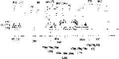
图1是根据本发明一实施例的用于LCD的TFT阵列面板的布局图;1 is a layout diagram of a TFT array panel for LCD according to an embodiment of the present invention;
图2是沿着线II-II得到的图1所示的TFT阵列面板的截面图;Fig. 2 is a sectional view of the TFT array panel shown in Fig. 1 obtained along the line II-II;
图3A、4A、5A和6A是布局图,依次示出了根据图1和图2实施例的用于LCD的TFT阵列面板的制造方法的中间步骤;3A, 4A, 5A and 6A are layout diagrams, showing in turn the intermediate steps of the manufacturing method for the TFT array panel for LCD according to the embodiment of FIG. 1 and FIG. 2;
图3B是沿着线IIIb-IIIb’得到的图3A所示的TFT阵列面板的截面图;Figure 3B is a sectional view of the TFT array panel shown in Figure 3A obtained along the line IIIb-IIIb';
图4B是在图3B所示步骤之后的步骤中,沿着线IVb-IVb’得到的图4A所示的TFT阵列面板的界面图;Fig. 4B is in the step after the step shown in Fig. 3B, the interface diagram of the TFT array panel shown in Fig. 4A obtained along the line IVb-IVb';
图5B是在图4B所示步骤之后的步骤中,沿着线Vb-Vb’得到的图5A所示的TFT阵列面板的界面图;Fig. 5 B is in the step after step shown in Fig. 4 B, the interface diagram of the TFT array panel shown in Fig. 5 A obtained along line Vb-Vb ';
图6B是在图5B所示步骤之后的步骤中,沿着线VIb-VIb’得到的图6A所示的TFT阵列面板的界面图;Fig. 6 B is in the step after step shown in Fig. 5 B, the interface diagram of the TFT array panel shown in Fig. 6 A obtained along line VIb-VIb ';
图7是根据本发明另一实施例的用于OLED的TFT阵列面板的布局图;7 is a layout diagram of a TFT array panel for an OLED according to another embodiment of the present invention;
图8A和8B分别是沿着线VIIIa-VIIIa’和线VIIIb-VIIIb’得到的图7所示的TFT阵列面板的截面图;Fig. 8 A and 8B are respectively the sectional view of the TFT array panel shown in Fig. 7 obtained along line VIIIa-VIIIa ' and line VIIIb-VIIIb ';
图9、11、13、15、17、19和21是在根据本发明一实施例的制造方法的中间步骤中,图7至8B所示的TFT阵列面板的布局图;Figures 9, 11, 13, 15, 17, 19 and 21 are layout views of the TFT array panel shown in Figures 7 to 8B in intermediate steps of the manufacturing method according to an embodiment of the present invention;
图10A和10B是沿着线Xa-Xa’和Xb-Xb’得到的图9所示的TFT阵列面板的截面图;Figures 10A and 10B are cross-sectional views of the TFT array panel shown in Figure 9 obtained along lines Xa-Xa' and Xb-Xb';
图12A和12B是沿着线XIIa-XIIa’和XIIb-XIIb’得到的图11所示的TFT阵列面板的截面图;12A and 12B are cross-sectional views of the TFT array panel shown in FIG. 11 obtained along lines XIIa-XIIa' and XIIb-XIIb';
图14A和14B是沿着线XIVa-XIVa’和XIVb-XIVb’得到的图13所示的TFT阵列面板的截面图;14A and 14B are cross-sectional views of the TFT array panel shown in FIG. 13 obtained along lines XIVa-XIVa' and XIVb-XIVb';
图16A和16B是沿着线XVIa-XVIa’和XVIb-XVIb’得到的图15所示的TFT阵列面板的截面图;16A and 16B are cross-sectional views of the TFT array panel shown in FIG. 15 obtained along lines XVIa-XVIa' and XVIb-XVIb';
图18A和18B是沿着线XVIIIa-XVIIIa’和XVIIIb-XVIIIb’得到的图17所示的TFT阵列面板的截面图;18A and 18B are cross-sectional views of the TFT array panel shown in FIG. 17 obtained along lines XVIIIa-XVIIIa' and XVIIIb-XVIIIb';
图20A和20B是沿着线XXa-XXa’和XXb-XXb’得到的图19所示的TFT阵列面板的截面图;以及20A and 20B are cross-sectional views of the TFT array panel shown in FIG. 19 obtained along lines XXa-XXa' and XXb-XXb'; and
图22A和22B是沿着线XXIIa-XXIIa’和XXIIb-XXIIb’得到的图21所示的TFT阵列面板的截面图。22A and 22B are cross-sectional views of the TFT array panel shown in FIG. 21 taken along lines XXIIa-XXIIa' and XXIIb-XXIIb'.
具体实施方式Detailed ways
下文中将参照其中示出了本发明优选实施例的附图更充分地描述本发明的优选实施例。然而,本发明可以以不同的形式实施,而不应解释为仅限于在此阐述的实施例。此外,提供这些实施例是为了使本公开全面而彻底,并将本发明的范围充分告知本领域技术人员。Preferred embodiments of the invention will be described more fully hereinafter with reference to the accompanying drawings, in which preferred embodiments of the invention are shown. However, this invention may be embodied in different forms and should not be construed as limited to only the embodiments set forth herein. Moreover, these embodiments are provided so that this disclosure will be thorough and thorough, and will fully convey the scope of the invention to those skilled in the art.
在附图中,为清楚起见,夸大了层、膜和区域的厚度。通篇用相同的附图标记表示相同的元件。应理解的是,当诸如层、膜、区域或基板的一个元件被称为在另一元件“上”时,其可以直接在另一元件上,或者,也可以存在插入元件。In the drawings, the thickness of layers, films and regions are exaggerated for clarity. The same reference numerals are used to refer to the same elements throughout. It will be understood that when an element such as a layer, film, region, or substrate is referred to as being "on" another element, it can be directly on the other element or intervening elements may also be present.
现在,将参照附图详细描述根据本发明实施例的用于LCD和OLED的TFT阵列面板及其制造方法。Now, a TFT array panel for LCDs and OLEDs and methods of manufacturing the same according to embodiments of the present invention will be described in detail with reference to the accompanying drawings.
实施例1Example 1
首先,参照图1和2详细描述根据本发明实施例的TFT阵列面板。First, a TFT array panel according to an embodiment of the present invention will be described in detail with reference to FIGS. 1 and 2 .
图1是根据本发明一实施例的用于LCD的TFT阵列面板的布局图;图2是沿着线II-II得到的图1所示的TFT阵列面板的截面图。1 is a layout diagram of a TFT array panel for an LCD according to an embodiment of the present invention; FIG. 2 is a cross-sectional view of the TFT array panel shown in FIG. 1 taken along line II-II.
用于传输栅极信号的多条栅极线121形成在绝缘基板110上。栅极线121主要形成在水平方向上并且其局部(partial portion)形成了多个栅电极124。而且,在向下方向上延伸的其不同的局部形成了多个延展部127。栅极线121的端部129具有扩大的宽度,用于与诸如驱动电路的外部装置连接。A plurality of
栅极线121具有第一层124p、127p、129p,第二层124q、127q、129q,以及第三层124r、127r、129r。第一层124p、127p、129p包括诸如ITO(氧化铟锡)或IZO(氧化铟锌)的导电氧化物,并且形成在基板110上。第二层124q、127q、129q包括形成在第一层124p、127p、129p上的含Cu金属,比如Cu和Cu合金。第三层124r、127r、129r包括形成在第二层124q、127q、129q上的导电氧化物,比如ITO或IZO。The
此处,第三层124r、127r、129r防止第二层124q、127q、129q的Cu扩散到形成在其上的栅极绝缘层140中。Here, the
当在Cu层与基板之间设置导电氧化物层时,增强了Cu层与基板之间的粘附性,从而防止了Cu层的剥落和抬起。When the conductive oxide layer is provided between the Cu layer and the substrate, the adhesion between the Cu layer and the substrate is enhanced, thereby preventing peeling and lifting of the Cu layer.
当所述导电氧化物层包括非晶ITO时,则更加显著地增强了Cu层与基板之间的粘附性。这是因为在低温下形成的非晶ITO层在后续栅极绝缘层140和半导体层151的形成期间要经受约200℃的高温,由此导致ITO层的结晶。When the conductive oxide layer includes amorphous ITO, the adhesion between the Cu layer and the substrate is more significantly enhanced. This is because the amorphous ITO layer formed at a low temperature is subjected to a high temperature of about 200° C. during subsequent formation of the
可以通过相同的蚀刻工艺来蚀刻Cu层和诸如ITO层或IZO层的导电氧化物层。由于Cu受到酸的强烈影响,所以当Cu暴露于酸时,其被非常迅速地蚀刻。因此,通常使用弱酸来蚀刻Cu层。然而,由于诸如Mo、Cr和Ti的其他金属被蚀刻得比Cu慢的多,当这样的金属用作Cu层的下层时,则应用两种不同的蚀刻条件以构图这些层。相反,由于非晶ITO或IZO与Cu层一起通过相同的蚀刻工艺被蚀刻,它们被同时构图以形成栅极线121。A Cu layer and a conductive oxide layer such as an ITO layer or an IZO layer can be etched by the same etching process. Since Cu is strongly affected by acids, it is etched very rapidly when Cu is exposed to acids. Therefore, a weak acid is usually used to etch the Cu layer. However, since other metals such as Mo, Cr and Ti are etched much slower than Cu, when such metals are used as underlying layers of the Cu layer, two different etching conditions are applied to pattern these layers. On the contrary, since the amorphous ITO or IZO is etched through the same etching process together with the Cu layer, they are simultaneously patterned to form the
第一层124p、127p、129p和第三层124r、127r、129r可以包括ITON层或IZON层以防止在第二层124q、127q、129q与第一层124p、127p、129p和第三层124r、127r、129r的界面处Cu的氧化。ITON层或IZON层通过将ITO层或IZO层暴露于氮气氛而形成并防止了由于Cu氧化所致的电阻的迅速增大。The
第三层124r、127r、129r,第二层124q、127q、129q以及第一层124p、127p、129p的横向侧面相对于基板110的表面倾斜,并且其倾角在约30至80度的范围内。The lateral sides of the
在栅极线121上形成有优选包括氮化硅(SiNx)的栅极绝缘层140。A
在栅极绝缘层140上形成多个半导体条151,其优选包括氢化非晶硅(缩写为“a-Si”)。每个半导体条151基本上沿纵向延伸,并且周期性地弯曲。每个半导体条151具有朝向栅电极124分支出来的多个突出体154。每个半导体条151的宽度在栅极线121附近变大,使得半导体条151覆盖住栅极线121的较大面积。A plurality of semiconductor strips 151 are formed on the
在半导体条151上形成多个欧姆接触条161和岛165,它们优选包括硅化物或者用n型杂质重掺杂的n+氢化a-Si。每个欧姆接触条161具有多个突出体163,并且突出体163和欧姆接触岛165在半导体条151的突出体154上成对设置。A plurality of ohmic contact strips 161 and
半导体条151以及欧姆接触161和165的横向侧面呈锥形,并且半导体151以及欧姆接触161和165的横向侧面的倾角优选处于约30至80度的范围内。The lateral sides of the
在欧姆接触161和165以及栅极绝缘层140上形成多个数据线171、多个漏电极175以及多个存储电容器导体177。A plurality of
用于传输数据电压的数据线171基本上沿着纵向延伸并且与栅极线121交叉,从而界定了呈矩阵排布的象素区域。每条数据线171具有朝向漏电极175突出的多个分支,形成了多个源电极173,并具有宽度增大的端部179。每对源电极173和漏电极175在栅电极124上相互分离,并且相互对置。The data lines 171 for transmitting data voltages substantially extend longitudinally and cross the
数据线171、漏电极175以及存储电容器导体177具有第一层171p、175p、177p,第二层171q、175q、177q,以及第三层171r、175r、177r。第一层171p、175p、177p和第三层171r、175r、177r分别设置在第二层171q、175q、177q的上下两侧。第一层171p、175p、177p和第三层171r、175r、177r包括导电氧化物。第二层171q、175q、177q包括含Cu金属,比如Cu或Cu合金。The
第一层171p、175p、177p和第三层171r、175r、177r可以包括ITO或IZO。此处,导电氧化物制成的第一层171p、175p、177p和第三层171r、175r、177r防止了第二层171q、175q、177q的Cu扩散到半导体层151和形成在其上的象素电极190中。当导电氧化物层包括ITO时,优选的是非晶ITO。由于非晶ITO或IZO与Cu一起通过相同的蚀刻工艺被蚀刻,其被同时构图以形成数据线171,数据线171具有平滑的轮廓而没有凹切(undercutting)。第一层171p、175p、177p和第三层171r、175r、177r优选包括ITON层或IZON层,以防止在第二层171q、175q、177q与第一层171p、175p、177p和第三层171r、175r、177r的界面处Cu的氧化。ITON层或IZON层通过将ITO层或IZO层暴露于氮气氛而形成,并有助于防止由于Cu氧化所致的电阻的迅速增大。The
栅电极124、源电极173以及漏电极175与半导体条151的突出体154一起,形成了TFT,该TFT具有形成于设置在源电极173与漏电极175之间的突出体154中的沟道。存储电容器导体177与栅极线121的延展部127重叠。The
数据线171、漏电极175以及存储电容器导体177具有锥形横向侧面,并且横向侧面的倾角处于约30至80度的范围内。The
欧姆接触161和165仅插入在半导体条151与数据线171之间和漏电极175与半导体条151的突出体154之间,以便降低它们之间的接触电阻。The
半导体条151部分地暴露在源电极173与漏电极175之间的位置,以及没有被数据线171和漏电极175覆盖的其他位置。半导体条151的大部分窄于数据线171,但是在半导体条151与栅极线121彼此相遇的位置附近半导体条151的宽度变大,以便防止数据线171的断开。The
在数据线171、漏电极175、存储电容器导体177以及半导体条151的暴露区域上,设置有钝化层180,该钝化层180包括具有相当的平坦化特性和感光度的有机材料,或者具有低介电常数的绝缘材料,比如a-Si:C:O,a-Si:O:F,等等。该钝化层180可以通过等离子体增强化学气相沉积(PECVD)工艺形成。为了防止钝化层180的有机材料与暴露于数据线171和漏电极175之间的半导体条151发生接触,该钝化层180可以以这样的方式构造而成,即在所述有机材料层下方额外地形成由SiNx或者SiO2制成的绝缘层。On the exposed areas of the
在钝化层180中,形成有多个接触孔181、185、187和182,以分别暴露出栅极线121的端部129、漏电极175、存储电容器导体177以及数据线171的端部179。In the
在钝化层180上形成包括IZO或ITO的多个接触辅助物(contactassistants)81和82和多个象素电极190。A plurality of
由于象素电极190分别通过接触孔185和187与漏电极175和存储电容器导体177物理地并且电气性地连接起来,所以象素电极190从漏电极175接收数据电压,并且将其传送至存储电容器导体177。Since the
其上施加有所述数据电压的象素电极190与其上施加有公共电压的对置面板(未示出)的公共电极(未示出)一起产生电场,从而使得液晶层中的液晶分子重新排列。The
还有,如上所述,象素电极190和所述公共电极一起形成电容器,以在TFT被关断之后存储并保持所接收的电压。该电容器将被称作“液晶电容器”。为了增强电压存储能力,设置有另一电容器,该电容器与所述液晶电容器并行连接,并且将被称作“存储电容器”。该存储电容器形成于象素电极190与相邻栅极线121的重叠部分处,其中所述栅极线121将被称作“在前栅极线(previous gate line)”。栅极线121的延展部127用于确保最大可能的重叠面积,并由此提高所述存储电容器的存储容量。存储电容器导体177连接在象素电极190上,并且与延展部127发生重叠,且被设置在钝化层180之下,从而使得象素电极190靠近在前栅极线121。Also, as described above, the
接触辅助物81和82分别连接至栅极线121的端部129和数据线171的端部179。接触辅助物81和82分别提供了栅极线121的端部129与诸如驱动集成电路的外部装置之间以及数据线171的端部179与外部装置之间的保护与补充粘附力。应用接触辅助物81和82是可选的,因为它们不是必要的元件。The
现将参照图3A至6B以及图1和2对TFT阵列面板的制造方法进行详细描述。A method of manufacturing a TFT array panel will now be described in detail with reference to FIGS. 3A to 6B and FIGS. 1 and 2 .
首先,如图3A和3B所示,在绝缘基板110上形成诸如ITO或IZO的导电氧化物的第一层,含Cu金属的第二层,以及诸如ITO或IZO的导电氧化物的第三层。First, as shown in FIGS. 3A and 3B , a first layer of conductive oxide such as ITO or IZO, a second layer containing Cu metal, and a third layer of conductive oxide such as ITO or IZO are formed on an insulating
第一层和第二层可以通过共溅射(co-sputtering)沉积而成。两个靶被安置在用于共溅射的同一溅射室中。一个靶包括导电氧化物,比如ITO或IZO。另一个靶包括含Cu金属,比如Cu或Cu合金。下文中,将描述ITO靶和Cu靶的实例。The first and second layers may be deposited by co-sputtering. Both targets were placed in the same sputtering chamber for co-sputtering. One target includes a conductive oxide, such as ITO or IZO. Another target includes a Cu-containing metal, such as Cu or a Cu alloy. Hereinafter, examples of an ITO target and a Cu target will be described.
所述共溅射工艺如下进行。The co-sputtering process is performed as follows.
首先,为了沉积第一ITO层,将功率施加至ITO靶,同时对Cu靶不施加功率。在25℃与150℃之间的温度下执行溅射同时供应氢气(H2)或水蒸汽(H2O)。这样的条件导致了非晶ITO层的形成。该ITO层具有50至500的厚度。First, to deposit the first ITO layer, power was applied to the ITO target while no power was applied to the Cu target. Sputtering is performed at a temperature between 25°C and 150°C while supplying hydrogen (H2 ) or water vapor (H2 O). Such conditions lead to the formation of an amorphous ITO layer. The ITO layer has a thickness of 50 Å to 500 Å.
接下来,通过切换功率使其施加到Cu靶而不施加到ITO靶来沉积Cu层。Cu层具有50至2000的厚度。Next, a Cu layer was deposited by switching the power to the Cu target and not the ITO target. The Cu layer has a thickness of 50 Å to 2000 Å.
接着,通过切换功率使其再次施加到ITO靶而不施加到Cu靶,来沉积第二ITO层。在25℃与150℃之间的温度下执行溅射同时供应氢气(H2)或水蒸汽(H2O)。这样的条件导致了非晶ITO层的形成。第二ITO层具有50至500的厚度。Next, a second ITO layer was deposited by switching the power again to the ITO target and not to the Cu target. Sputtering is performed at a temperature between 25°C and 150°C while supplying hydrogen (H2 ) or water vapor (H2 O). Such conditions lead to the formation of an amorphous ITO layer. The second ITO layer has a thickness of 50 Å to 500 Å.
在溅射ITO靶时,可以施加氮气(N2)、一氧化二氮(N2O)或氨(NH3),以形成ITON层。Nitrogen (N2 ), nitrous oxide (N2 O), or ammonia (NH3 ) may be applied when sputtering an ITO target to form an ITON layer.
当在Cu层与基板之间设置导电氧化物层时,增强了Cu层与基板之间的粘附性。施加在Cu层顶部的导电氧化物层防止了Cu扩散到将要形成在其上的栅极绝缘层140中。When the conductive oxide layer is provided between the Cu layer and the substrate, the adhesion between the Cu layer and the substrate is enhanced. The conductive oxide layer applied on top of the Cu layer prevents Cu from diffusing into the
当所述导电氧化物层包括非晶ITO时,则显著地增强了Cu层与基板110之间的粘附性。这是因为在低温下形成的非晶ITO层在栅极绝缘层140和半导体层151的形成期间要经受约200℃的高温,由此导致了ITO层的结晶。When the conductive oxide layer includes amorphous ITO, the adhesion between the Cu layer and the
可以通过弱酸来蚀刻非晶ITO层或非晶IZO层。由于Cu受到酸的强烈影响,所以其被非常迅速地蚀刻。因此,通常使用弱酸来蚀刻Cu层。然而,由于诸如Mo、Cr和Ti的其他金属被蚀刻得比Cu慢的多,所以当这样的金属用作Cu层的下层时,则应用两种不同的蚀刻条件以构图这些层。相反,由于非晶ITO或IZO与Cu层一起被弱酸蚀刻,所以这些层被同时构图以形成栅极线121。The amorphous ITO layer or the amorphous IZO layer can be etched by weak acid. Since Cu is strongly affected by acid, it is etched very rapidly. Therefore, a weak acid is usually used to etch the Cu layer. However, since other metals such as Mo, Cr and Ti are etched much slower than Cu, when such metals are used as the underlying layer of the Cu layer, two different etching conditions are applied to pattern these layers. In contrast, since the amorphous ITO or IZO is etched with weak acid together with the Cu layer, these layers are simultaneously patterned to form the
如上所述,当在Cu层与基板之间设置非晶ITO或IZO层时,增强了Cu层与基板之间的粘附性以及蚀刻效率。非晶ITO或IZO层防止了Cu扩散到其他层中。As described above, when the amorphous ITO or IZO layer is provided between the Cu layer and the substrate, the adhesion between the Cu layer and the substrate and the etching efficiency are enhanced. The amorphous ITO or IZO layer prevents Cu from diffusing into other layers.
当在ITO或IZO靶的溅射期间供应氮气(N2)、一氧化二氮(N2O)或氨(NH3)时,形成了ITON或IZON层,从而防止了界面处Cu层的氧化。When nitrogen gas (N2 ), nitrous oxide (N2O ), or ammonia (NH3 ) is supplied during sputtering of ITO or IZO targets, an ITON or IZON layer is formed, preventing oxidation of the Cu layer at the interface .
然后,在第二ITO层上涂敷光致抗蚀剂,并通过光掩模用光来照射光致抗蚀剂。接着,显影被照射的光致抗蚀剂。Then, a photoresist is coated on the second ITO layer, and the photoresist is irradiated with light through a photomask. Next, the irradiated photoresist is developed.
利用蚀刻剂同时蚀刻两个ITO层以及Cu层以形成多个栅极线121,该蚀刻剂比如是过氧化氢(H2O2),或者包含适量的磷酸(H2PO3)、硝酸(HNO3)和醋酸(CH3COOH)的普通蚀刻剂。A plurality of
如图3A和3B所示,通过上述工艺,形成了多个栅极线121,其具有多个栅电极124、延展部127和端部129。As shown in FIGS. 3A and 3B , through the above process, a plurality of
参照图4A和4B,在栅极绝缘层140、本征a-Si层以及非本征a-Si层被依次沉积之后,对非本征a-Si层和本征a-Si层进行光蚀刻(photo-etched),以形成多个非本征半导体条161和多个本征半导体条151,它们分别具有突出体164和154。栅极绝缘层140优选包括氮化硅,其厚度为约2000至约5000,并且沉积温度优选处于约250℃至约500℃之间的范围内。Referring to FIGS. 4A and 4B, after the
由于这一工艺在200℃以上的高温下执行,所以将栅极线121的非晶ITO结晶。Since this process is performed at a high temperature of 200° C. or higher, the amorphous ITO of the
接着,在非本征半导体条161上依次沉积诸如ITO的导电氧化物的第一层,含Cu金属的第二层,以及诸如ITO的导电氧化物的第三层。Next, a first layer of a conductive oxide such as ITO, a second layer of Cu metal, and a third layer of a conductive oxide such as ITO are sequentially deposited on the extrinsic semiconductor strips 161 .
导电氧化物的第一层和第三层防止了第二层的Cu扩散到其上将要形成的半导体层151和象素电极190中。The first and third layers of the conductive oxide prevent Cu of the second layer from diffusing into the
第一层和第三层可以包括ITO或IZO。当第一层和第三层由ITO形成时,在25℃与150℃之间的温度下执行溅射同时供应氢气(H2O)或水蒸汽(H2O)。这一操作条件导致非晶ITO层的形成。The first and third layers may include ITO or IZO. When the first and third layers are formed of ITO, sputtering is performed at a temperature between 25° C. and 150° C. while supplying hydrogen gas (H2 O) or water vapor (H2 O). This operating condition results in the formation of an amorphous ITO layer.
由于非晶ITO或IZO可以与Cu层一起通过弱酸被蚀刻,所以可以同时构图这些层。Since amorphous ITO or IZO can be etched together with the Cu layer by weak acid, these layers can be patterned simultaneously.
当在ITO或IZO靶的溅射期间供应氮气(N2)、一氧化二氮(N2O)或氨(NH3)时,形成了ITON或IZON层,用于防止界面处Cu层的氧化。When nitrogen gas (N2 ), nitrous oxide (N2 O) or ammonia (NH3 ) is supplied during sputtering of an ITO or IZO target, an ITON or IZON layer is formed for preventing oxidation of the Cu layer at the interface .
第一和第三层形成为具有约50至500的厚度,并且第二层形成为具有约1500至3000的厚度。The first and third layers are formed to have a thickness of about 50 Å to 500 Å, and the second layer is formed to have a thickness of about 1500 Å to 3000 Å.
然后,在第三层上涂敷光致抗蚀剂,并通过光掩模用光来照射光致抗蚀剂。接着,显影被照射的光致抗蚀剂。Then, a photoresist is coated on the third layer, and the photoresist is irradiated with light through a photomask. Next, the irradiated photoresist is developed.
利用蚀刻剂同时蚀刻第一至第三层以形成多个数据线171,该蚀刻剂比如是过氧化氢(H2O2),或者包含适量的磷酸(H2PO3)、硝酸(HNO3)和醋酸(CH3COOH)的普通蚀刻剂。A plurality of
如图5A和5B所示,通过上述工艺,形成了多个数据线171和存储电容器导体177,数据线171具有多个源电极173、多个漏电极175和端部179。As shown in FIGS. 5A and 5B , through the above process, a plurality of
接着,通过蚀刻去除没有被数据线171和漏电极175覆盖的非本征半导体条161部分,以形成多个欧姆接触163和165,并且暴露出部分本征半导体条151。可以随后进行氧等离子体处理,以便稳定半导体条151的暴露表面。Next, the portion of the
参照图6A和6B,钝化层180被沉积并且与栅极绝缘层140一起被干法蚀刻,以形成多个接触孔181、185、187和182。栅极绝缘层140和钝化层180优选在这样的蚀刻条件下被蚀刻,即对于栅极绝缘层140和钝化层180来说具有基本上相同的蚀刻比率。Referring to FIGS. 6A and 6B , a
当钝化层包括光敏材料时,可以仅利用光刻来形成接触孔,而没有后续的蚀刻步骤。When the passivation layer includes a photosensitive material, the contact hole may be formed using only photolithography without a subsequent etching step.
接着,在钝化层180上将氧化铟锡(ITO)层沉积至约400至1500的厚度并对其构图,以形成多个象素电极190和接触辅助物81和82。Next, an indium tin oxide (ITO) layer is deposited to a thickness of about 400 Å to 1500 Å on the
在本实施例中,ITO是主要的导电氧化物,但也可以使用诸如IZO的其他导电氧化物来作为本发明的导电氧化物。In this embodiment, ITO is the main conductive oxide, but other conductive oxides such as IZO can also be used as the conductive oxide in the present invention.
在本实施例中,在Cu层的下侧和上侧设置导电氧化物层。然而,也可以省略上部和下部导电氧化物层之一。In this embodiment, conductive oxide layers are provided on the lower and upper sides of the Cu layer. However, one of the upper and lower conductive oxide layers may also be omitted.
实施例2Example 2
现在,将描述根据本发明另一实施例的用于有源矩阵有机发光显示器(AM-OLED)的TFT面板。Now, a TFT panel for an active matrix organic light emitting display (AM-OLED) according to another embodiment of the present invention will be described.
图7是根据本发明另一实施例的用于OLED的TFT阵列面板的布局图。图8A和8B分别是沿着线VIIIa-VIIIa’和线VIIIb-VIIIb’得到的图7所示的TFT阵列面板的截面图。FIG. 7 is a layout diagram of a TFT array panel for an OLED according to another embodiment of the present invention. 8A and 8B are cross-sectional views of the TFT array panel shown in FIG. 7 taken along line VIIIa-VIIIa' and line VIIIb-VIIIb', respectively.
在诸如透明玻璃的绝缘基板110上形成多个栅极导体(gateconductors),所述栅极导体包括多个栅极线121,所述多个栅极线121包括多个第一栅电极124a和多个第二栅电极124b。A plurality of gate conductors (gate conductors) are formed on an insulating
传输栅极信号的栅极线121基本上沿着横向延伸,并且相互分离。第一栅电极124a向上突伸,如从图7所示的透视图所看到的那样。栅极线121可以延伸以连接于集成在基板110上的驱动电路(未示出)。可选择地,栅极线121可以具有大面积的端部(未示出),用于与安装在基板110或者另一装置上的外部驱动电路或另一层连接,或在另一装置上,所述另一装置比如是可以附着到基板110上的柔性印刷电路膜(未示出)。The gate lines 121 transmitting gate signals extend substantially in a lateral direction and are separated from each other. The
每个第二栅电极124b与栅极线121分离,并且包括在两条相邻栅极线121之间基本上横向延伸的存储电极133。Each
栅极线121、第一栅电极124a和第二栅电极124b以及存储电极133具有第一层124ap、124bp、133p,形成在第一层124ap、124bp、133p上的第二层124aq、124bq、133q,以及形成在第二层124aq、124bq、133q上的第三层124ar、124br、133r。第一层124ap、124bp、133p包括诸如ITO或IZO的导电氧化物。第二层124aq、124bq、133q包括含Cu金属,比如Cu或Cu合金。第三层124ar、124br、133r包括导电氧化物,比如ITO或IZO。The
此处,第三层124ar、124br、133r防止第二层124aq、124bq、133q的Cu扩散到形成在其上的栅极绝缘层140中。Here, the third layers 124ar, 124br, 133r prevent Cu of the second layers 124aq, 124bq, 133q from diffusing into the
当在Cu层与基板之间设置导电氧化物层时,增强了Cu层与基板之间的粘附性,从而防止了Cu层的剥落和抬起。When the conductive oxide layer is provided between the Cu layer and the substrate, the adhesion between the Cu layer and the substrate is enhanced, thereby preventing peeling and lifting of the Cu layer.
当所述导电氧化物层包括非晶ITO时,则显著地增强了Cu层与基板之间的粘附性。这是因为在低温下形成的非晶ITO层在栅极绝缘层140和半导体层151的形成期间要经受约200℃的高温,由此导致ITO层的结晶。When the conductive oxide layer includes amorphous ITO, the adhesion between the Cu layer and the substrate is significantly enhanced. This is because the amorphous ITO layer formed at a low temperature is subjected to a high temperature of about 200° C. during the formation of the
可以通过相同的蚀刻工艺来蚀刻Cu层和诸如ITO层或IZO层的导电氧化物层。由于Cu受到酸的强烈影响,所以当Cu暴露于酸时,其被非常迅速地蚀刻。因此,通常使用弱酸来蚀刻Cu层。然而,由于诸如Mo、Cr和Ti的其他金属被蚀刻得比Cu慢的多,所以当这样的金属用作Cu层的下层时,则应用两种不同的蚀刻条件以构图这些层。相反,由于非晶ITO或IZO与Cu层一起通过相同的蚀刻工艺被蚀刻,它们被同时构图以形成栅极线121。A Cu layer and a conductive oxide layer such as an ITO layer or an IZO layer can be etched by the same etching process. Since Cu is strongly affected by acids, it is etched very rapidly when Cu is exposed to acids. Therefore, a weak acid is usually used to etch the Cu layer. However, since other metals such as Mo, Cr and Ti are etched much slower than Cu, when such metals are used as the underlying layer of the Cu layer, two different etching conditions are applied to pattern these layers. On the contrary, since the amorphous ITO or IZO is etched through the same etching process together with the Cu layer, they are simultaneously patterned to form the
第一层124ap、124bp、133p和第三层124ar、124br、133r可以包括ITON层或IZON层以防止在第二层124aq、124bq、133q与第一层124ap、124bp、133p和第三层124ar、124br、133r的界面处Cu的氧化。ITON层或IZON层通过将ITO层或IZO层暴露于氮气氛而形成,并有助于防止由于Cu氧化所致的电阻的迅速增大。The first layer 124ap, 124bp, 133p and the third layer 124ar, 124br, 133r may include an ITON layer or an IZON layer to prevent the Oxidation of Cu at the interface of 124br, 133r. The ITON layer or the IZON layer is formed by exposing the ITO layer or the IZO layer to a nitrogen atmosphere, and helps prevent rapid increase in resistance due to Cu oxidation.
此外,栅极导体121和124b的横向侧面相对于基板110的表面倾斜,并且其倾角的范围约为30至80度。优选包括氮化硅(SiNx)的栅极绝缘层140形成在栅极导体121和124b上。In addition, the lateral sides of the
在栅极绝缘层140上形成多个半导体条151和岛154b,其优选包括氢化非晶硅(缩写为“a-Si”)。每个半导体条151基本上沿着纵向延伸,并且具有朝向第一栅电极124a分支出来的多个突出体154a。每个半导体岛154b与第二栅电极124b相交,并且包括与第二栅电极124b的存储电极133重叠的部分157。A plurality of semiconductor strips 151 and
在半导体条151和岛154b上形成多个欧姆接触条161和欧姆接触岛163b、165a和165b,它们优选包括硅化物或者利用诸如磷的n型杂质重掺杂的n+氢化a-Si。每个欧姆接触条161具有多个突出体163a,并且突出体163a和欧姆接触岛165a在半导体条151的突出体154a上成对设置。欧姆接触岛163b和165b在半导体岛154b上成对设置。A plurality of ohmic contact strips 161 and
半导体条151和岛154b以及欧姆接触161、163b、165b以及165b的横向侧面相对于基板的表面倾斜,并且其倾角优选处于约30至8O度之间的范围内。The lateral sides of semiconductor strips 151 and
在欧姆接触161、163b、165b和165b以及栅极绝缘层140上形成包括多个数据线171、多个电压传输线172以及多个第一和第二漏电极175a和175b的多个数据导体。A plurality of data conductors including a plurality of
用于传输数据信号的数据线171基本上沿着纵向延伸,并且与栅极线121交叉。每个数据线171包括多个第一源电极173a和具有大面积的端部,该端部用于与另一层或者外部装置发生接触。数据线171可以直接连接到用于产生栅极信号的数据驱动电路上,所述数据驱动电路可以被集成在基板110上。The data lines 171 for transmitting data signals extend substantially in a longitudinal direction and cross the gate lines 121 . Each
用于传输驱动电压的电压传输线172基本上沿着纵向延伸,并且与栅极线121交叉。每个电压传输线172包括多个第二源电极173b。电压传输线172可以相互连接。电压传输线172与半导体岛154b的存储区域157重叠。The
第一漏电极175a和第二漏电极175b与数据线171和电压传输线172分离,并且相互分离开。每对第一源电极173a和第一漏电极175a相对于第一栅电极124a彼此相对地设置,并且每对第二源电极173b和第二漏电极175b相对于第二栅电极124b彼此相对地设置。The
第一栅电极124a、第一源电极173a以及第一漏电极175a与半导体条151的突出体154a一起,形成了开关TFT,其具有形成于设置在第一源电极173a与第一漏电极175a之间的突出体154a中的沟道。同时,第二栅电极124b、第二源电极173b以及第二漏电极175b与半导体岛154b一起,形成了驱动TFT,其具有形成于设置在第二源电极173b与第二漏电极175b之间的半导体岛154b中的沟道。The
数据导体171、172、175a、175b优选具有第一层171p、172p、175ap、175bp,第二层171q、172q、175aq、175bq,以及第三层171r、172r、175ar、175br。第二层171q、172q、175aq、175bq包括含Cu金属,比如Cu或Cu合金。第一层171p、172p、175ap、175bp和第三层171r、172r、175ar、175br分别设置在第二层171q、172q、175aq、175bq的上下两侧。第一层171p、172p、175ap、175bp和第三层171r、172r、175ar、175br包括导电氧化物。The
第一层171p、172p、175ap、175bp和第三层171r、172r、175ar、175br可以包括ITO或IZO。此处,第一层171p、172p、175ap、175bp和第三层171r、172r、175ar、175br包括导电氧化物以防止第二层171q、172q、175aq、175bq的Cu扩散到半导体层151和形成在其上的象素电极190中。当导电氧化物层包括ITO时,优选的是非晶ITO。由于非晶ITO或IZO与Cu一起通过相同的蚀刻工艺被蚀刻,所以这些层被同时构图以形成具有平滑轮廓的数据线171。The
第一层171p、172p、175ap、175bp和第三层171r、172r、175ar、175br优选包括ITON层或IZON层,以防止在第二层171q、172q、175aq、175bq与第一层171p、172p、175ap、175bp和第三层171r、172r、175ar、175br的界面处Cu的氧化。ITON层或IZON层通过将ITO层或IZO层暴露于氮气氛而形成,并防止了由于Cu氧化所致的电阻的迅速增大。The
类似于栅极导体121和124b,数据导体171、172、175a和175b相对于基板110的表面具有锥形的横向侧面,并且其倾角处于约30至80度的范围内。Similar to the
欧姆接触161、163b、165b和165b仅插入在下层半导体条151和岛154b与其上的上层数据导体171、172、175a和175b之间,并且降低了它们之间的接触电阻。半导体条151包括没有被数据导体171、172、175a和175b覆盖的多个暴露部分。The
大部分半导体条151窄于数据线171,但是在半导体条151与栅极线121彼此相遇的位置附近,半导体151的宽度变大,以便防止数据线171的断开,如前所述。Most of the semiconductor strips 151 are narrower than the
在数据导体171、172、175a、175b以及半导体条151的暴露部分和岛154b上,形成钝化层180。该钝化层180优选包括诸如氮化硅或氧化硅的无机材料、具有良好平面度特性的光敏有机材料、或者诸如a-Si:C:O和a-Si:O:F的介电常数低于4.0的低介电绝缘材料,比如通过等离子体增强化学气相沉积(PECVD)而形成的a-Si:C:O和a-Si:O:F。该钝化层180可以包括无机绝缘体的下层膜和有机绝缘体的上层膜。On the
钝化层180具有多个接触孔189、183、185、181和182,分别暴露出部分第一漏电极175a、第二栅电极124b、第二漏电极175b以及栅极线121的端部129和数据线171的端部179。The
接触孔181和182暴露出栅极线121的端部129和数据线171的端部179,用以在栅极线121和数据线171与外部驱动电路之间提供连接。在所述外部驱动电路的输出端与端部129和179之间设置各向异性导电膜,用以辅助电连接和物理附着。但是,当驱动电路被直接制造在基板110上时,则不形成接触孔。在其中栅极驱动电路被直接制造在基板110上同时数据驱动电路作为单独的芯片形成的实施例中,仅形成暴露数据线171的端部179的接触孔181。The contact holes 181 and 182 expose the
在钝化层180上形成多个象素电极190、多个连接构件192以及多个接触辅助物81和82。A plurality of
象素电极190通过接触孔185连接到第二漏电极175b上。连接构件192通过接触孔189和183将第一漏电极175a和第二栅电极124b连接起来。接触辅助物81和82分别通过接触孔181和182连接到栅极线121的端部129和数据线171的端部179上。The
象素电极190、连接构件192以及接触辅助物81和82包括诸如ITO或者IZO的透明导体。The
在钝化层180和象素电极190上形成隔离物(partition)803、辅助电极272、多个发光构件70以及公共电极270。A
隔离物803包括有机或者无机绝缘材料,并且形成了有机发光单元的框架。隔离物803沿着象素电极190的边界形成,并且界定用于填充有机发光材料的空间。The
发光构件70设置在象素电极190上,并且由隔离物803环绕。发光构件70包括发出红色、绿色或者蓝色光的一种发光材料。红色、绿色和蓝色发光构件70被依次并重复地设置。The
辅助电极272具有与隔离物803基本上相同的平面图案。辅助电极272与公共电极270接触,以降低公共电极270的电阻。The
公共电极270形成在隔离物803、辅助电极272以及发光构件70上。公共电极270包括诸如Al的金属,其具有低的电阻率。本实施例示出了背侧发光OLED。但是,在包括前侧发光OLED或者双侧发光OLED的实施例中,公共电极270包括诸如ITO或者IZO的透明导体。The
现将参照图9A至22B以及图7至8B详细描述根据本发明一实施例的图7至8B所示的TFT阵列面板的制造方法。A method of manufacturing the TFT array panel shown in FIGS. 7 to 8B according to an embodiment of the present invention will now be described in detail with reference to FIGS. 9A to 22B and FIGS. 7 to 8B.
图9、11、13、15、17、19和21是在根据本发明一实施例的制造方法的中间步骤中,图7至8B所示的TFT阵列面板的布局图。图10A和10B是沿着线Xa-Xa’和Xb-Xb’得到的图9所示的TFT阵列面板的截面图。图12A和12B是沿着线XIIa-XIIa’和XIIb-XIIb’得到的图11所示的TFT阵列面板的截面图。图14A和14B是沿着线XIVa-XIVa’和XIVb-XIVb’得到的图13所示的TFT阵列面板的截面图。图16A和16B是沿着线XVIa-XVIa’和XVIb-XVIb’得到的图15所示的TFT阵列面板的截面图。图18A和18B是沿着线XVIIIa-XVIIIa’和XVIIIb-XVIIIb’得到的图17所示的TFT阵列面板的截面图。图20A和20B是沿着线XXa-XXa’和XXb XXb’得到的图19所示的TFT阵列面板的截面图。图22A和22B是沿着线XXIIa-XXIIa’和XXIIb-XXIIb’得到的图21所示的TFT阵列面板的截面图。9 , 11 , 13 , 15 , 17 , 19 and 21 are layout views of the TFT array panel shown in FIGS. 7 to 8B in intermediate steps of the manufacturing method according to an embodiment of the present invention. 10A and 10B are cross-sectional views of the TFT array panel shown in FIG. 9 taken along lines Xa-Xa' and Xb-Xb'. 12A and 12B are cross-sectional views of the TFT array panel shown in FIG. 11 taken along lines XIIa-XIIa' and XIIb-XIIb'. 14A and 14B are cross-sectional views of the TFT array panel shown in FIG. 13 taken along lines XIVa-XIVa' and XIVb-XIVb'. 16A and 16B are cross-sectional views of the TFT array panel shown in FIG. 15 taken along lines XVIa-XVIa' and XVIb-XVIb'. 18A and 18B are cross-sectional views of the TFT array panel shown in FIG. 17 taken along lines XVIIIa-XVIIIa' and XVIIIb-XVIIIb'. 20A and 20B are cross-sectional views of the TFT array panel shown in FIG. 19 taken along lines XXa-XXa' and XXb XXb'. 22A and 22B are cross-sectional views of the TFT array panel shown in FIG. 21 taken along lines XXIIa-XXIIa' and XXIIb-XXIIb'.
首先,如图9和10B所示,在绝缘基板110上形成诸如ITO或IZO的导电氧化物的第一层,含Cu金属的第二层,以及诸如ITO或IZO的导电氧化物的第三层。First, as shown in FIGS. 9 and 10B, a first layer of a conductive oxide such as ITO or IZO, a second layer containing Cu metal, and a third layer of a conductive oxide such as ITO or IZO are formed on an insulating
第一层和第二层可以通过共溅射沉积而成。两个靶被安置在用于共溅射的同一溅射室中。一个靶包括导电氧化物,比如ITO或IZO,另一个靶包括含Cu金属,比如Cu或Cu合金。下文中,将描述ITO靶和Cu靶的实例。The first and second layers can be deposited by co-sputtering. Both targets were placed in the same sputtering chamber for co-sputtering. One target comprises a conductive oxide, such as ITO or IZO, and the other target comprises a Cu-containing metal, such as Cu or a Cu alloy. Hereinafter, examples of an ITO target and a Cu target will be described.
所述共溅射工艺如下进行。The co-sputtering process is performed as follows.
首先,为了沉积第一ITO层,将功率施加至ITO靶,同时对Cu靶不施加功率。在25℃与150℃之间的温度下执行溅射同时供应氢气(H2)或水蒸汽(H2O)。这样的条件导致了非晶ITO层的形成。该ITO层具有50至500的厚度。First, to deposit the first ITO layer, power was applied to the ITO target while no power was applied to the Cu target. Sputtering is performed at a temperature between 25°C and 150°C while supplying hydrogen (H2 ) or water vapor (H2 O). Such conditions lead to the formation of an amorphous ITO layer. The ITO layer has a thickness of 50 Å to 500 Å.
接下来,通过切换功率使其施加到Cu靶而不施加到ITO靶来沉积Cu层。Cu层具有50至2000的厚度。Next, a Cu layer was deposited by switching the power to the Cu target and not the ITO target. The Cu layer has a thickness of 50 Å to 2000 Å.
接着,通过切换功率使其再次施加到ITO靶而不施加到Cu靶,来沉积第二ITO层。在25℃与150℃之间的温度下执行溅射同时供应氢气(H2)或水蒸汽(H2O)。这样的条件导致了非晶ITO层的形成。第二ITO层具有50至500的厚度。Next, a second ITO layer was deposited by switching the power again to the ITO target and not to the Cu target. Sputtering is performed at a temperature between 25°C and 150°C while supplying hydrogen (H2 ) or water vapor (H2 O). Such conditions lead to the formation of an amorphous ITO layer. The second ITO layer has a thickness of 50 Å to 500 Å.
在溅射ITO靶期间,可以施加氮气(N2)、一氧化二氮(N2O)或氨(NH3),以形成ITON层。During sputtering of the ITO target, nitrogen (N2 ), nitrous oxide (N2 O), or ammonia (NH3 ) may be applied to form an ITON layer.
当在Cu层与基板之间设置导电氧化物层时,增强了Cu层与基板之间的粘附性。施加在Cu层顶部的导电氧化物层防止了Cu扩散到将要形成在其上的栅极绝缘层140中。When the conductive oxide layer is provided between the Cu layer and the substrate, the adhesion between the Cu layer and the substrate is enhanced. The conductive oxide layer applied on top of the Cu layer prevents Cu from diffusing into the
当所述导电氧化物层包括非晶ITO时,则显著地增强了Cu层与基板110之间的粘附性。这是因为在低温下形成的非晶ITO层在栅极绝缘层140和半导体层151的形成期间要经受约200℃的高温,由此导致了ITO层的结晶。When the conductive oxide layer includes amorphous ITO, the adhesion between the Cu layer and the
可以通过弱酸来蚀刻非晶ITO层或非晶IZO层。由于Cu受到酸的强烈影响,所以其被非常迅速地蚀刻。因此,通常使用弱酸来蚀刻Cu层。然而,由于诸如Mo、Cr和Ti的其他金属被蚀刻得比Cu慢的多,所以当这样的金属用作Cu层的下层时,则应用两种不同的蚀刻条件以构图这些层。相反,由于非晶ITO或IZO与Cu层一起被弱酸蚀刻,所以这些层被同时构图以形成栅极线121、第二栅电极124b以及电压传输线172。The amorphous ITO layer or the amorphous IZO layer can be etched by weak acid. Since Cu is strongly affected by acid, it is etched very rapidly. Therefore, a weak acid is usually used to etch the Cu layer. However, since other metals such as Mo, Cr and Ti are etched much slower than Cu, when such metals are used as the underlying layer of the Cu layer, two different etching conditions are applied to pattern these layers. In contrast, since the amorphous ITO or IZO is etched with weak acid together with the Cu layer, these layers are simultaneously patterned to form the
如上所述,当在Cu层与基板之间设置非晶ITO或IZO层时,增强了Cu层与基板之间的粘附性以及蚀刻效率。非晶ITO或IZO层防止了Cu扩散到其他层中。As described above, when the amorphous ITO or IZO layer is provided between the Cu layer and the substrate, the adhesion between the Cu layer and the substrate and the etching efficiency are enhanced. The amorphous ITO or IZO layer prevents Cu from diffusing into other layers.
当在ITO或IZO靶的溅射期间供应氮气(N2)、一氧化二氮(N2O)或氨(NH3)时,形成了ITON或IZON层,从而防止了界面处Cu层的氧化。When nitrogen gas (N2 ), nitrous oxide (N2O ), or ammonia (NH3 ) is supplied during sputtering of ITO or IZO targets, an ITON or IZON layer is formed, preventing oxidation of the Cu layer at the interface .
然后,在第二ITO层上涂敷光致抗蚀剂,并通过光掩模用光来照射光致抗蚀剂。接着,显影被照射的光致抗蚀剂。Then, a photoresist is coated on the second ITO layer, and the photoresist is irradiated with light through a photomask. Next, the irradiated photoresist is developed.
利用蚀刻剂同时蚀刻两个ITO层以及Cu层以形成多个栅极线121、第二栅电极124b以及电压传输线172。该蚀刻剂可以是过氧化氢(H2O2)或者包含适量的磷酸(H2PO3)、硝酸(HNO3)和醋酸(CH3COOH)的普通蚀刻剂中的一种。The two ITO layers and the Cu layer are simultaneously etched using an etchant to form a plurality of
参照图11至12B,在栅极绝缘层140、本征a-Si层以及非本征a-Si层被依次沉积之后,对非本征a-Si层和本征a-Si层进行光蚀刻,以形成多个非本征半导体条164和包括栅极绝缘层140上的突出体154a的多个本征半导体条151以及岛154b。栅极绝缘层140优选包括氮化硅,其厚度为约2000至约5000,并且沉积温度优选处于约250℃至约500℃之间的范围内。Referring to FIGS. 11 to 12B, after the
由于这一工艺在200℃以上的高温下执行,所以将栅极线121的非晶ITO结晶。Since this process is performed at a high temperature of 200° C. or higher, the amorphous ITO of the
接着,参照图13至14B,在非本征半导体条161上依次沉积诸如ITO的导电氧化物的第一层,合Cu金属的第二层,以及诸如ITO的导电氧化物的第三层。Next, referring to FIGS. 13 to 14B , a first layer of a conductive oxide such as ITO, a second layer of a Cu metal, and a third layer of a conductive oxide such as ITO are sequentially deposited on the
导电氧化物的第一层和第三层防止了第二层的Cu扩散到其上将要形成的半导体层151和象素电极190中。The first and third layers of the conductive oxide prevent Cu of the second layer from diffusing into the
第一层和第三层可以包括ITO或IZO。当第一层和第三层由ITO形成时,在25℃与150℃之间的温度下执行溅射同时供应氢气(H2O)或水蒸汽(H2O)。这一操作条件导致非晶ITO层的形成。The first and third layers may include ITO or IZO. When the first and third layers are formed of ITO, sputtering is performed at a temperature between 25° C. and 150° C. while supplying hydrogen gas (H2 O) or water vapor (H2 O). This operating condition results in the formation of an amorphous ITO layer.
由于非晶ITO或IZO可以与Cu层一起被弱酸蚀刻,所以可以同时构图这些层。Since amorphous ITO or IZO can be etched by weak acid together with the Cu layer, these layers can be patterned simultaneously.
当在ITO或IZO靶的溅射期间供应氮气(N2)、一氧化二氮(N2O)或氨(NH3)时,形成了ITON或IZON层,以用于防止界面处Cu层的氧化。When nitrogen (N2 ), nitrous oxide (N2 O) or ammonia (NH3 ) is supplied during sputtering of an ITO or IZO target, an ITON or IZON layer is formed for preventing the Cu layer at the interface from oxidation.
第一和第三层形成为具有约50至500的厚度,并且第二层形成为具有约1500至3000的厚度。The first and third layers are formed to have a thickness of about 50 Å to 500 Å, and the second layer is formed to have a thickness of about 1500 Å to 3000 Å.
然后,在第三层上涂敷光致抗蚀剂,并通过光掩模用光来照射光致抗蚀剂。接着,显影被照射的光致抗蚀剂。Then, a photoresist is coated on the third layer, and the photoresist is irradiated with light through a photomask. Next, the irradiated photoresist is developed.
利用蚀刻剂同时蚀刻第一至第三层以形成多个数据线171,该蚀刻剂比如是过氧化氢(H2O2),或者包含适量的磷酸(H2PO3)、硝酸(HNO3)和醋酸(CH3COOH)的普通蚀刻剂。A plurality of
如图13和14B所示,通过上述工艺,形成了具有多个第一源电极173a的多个数据线171、多个第一和第二漏电极175a和175b,以及具有第二源电极173b的多个电压传输线172。As shown in FIGS. 13 and 14B, through the above process, a plurality of
在去除光致抗蚀剂之前或之后,通过蚀刻去除没有被数据导体171、172、175a和175b覆盖的非本征半导体条164部分,以形成包括突出体163a的多个欧姆接触条161以及多个欧姆接触岛163b、165a和165b,并且暴露出部分本征半导体条151和岛154b。Before or after removing the photoresist, the parts of the extrinsic semiconductor strips 164 not covered by the
可以随后进行氧等离子体处理,以便稳定半导体条151的暴露表面。An oxygen plasma treatment may then be performed in order to stabilize the exposed surfaces of the semiconductor strips 151 .
参照图15至16B,钝化层180由有机绝缘材料或无机绝缘材料形成。由于在200℃以上的高温下执行这一工艺,所以将数据导体171、172、175a和175b的非晶ITO结晶。15 to 16B, the
构图钝化层180,以形成多个接触孔189、185、183、181和182,所述多个接触孔分别暴露出第一漏电极175a、第二漏电极175b、第二栅电极124b、栅极线121的端部129以及数据线171的端部179。The
参照图17至18B,在钝化层180上形成包括ITO或IZO的接触辅助物81和82、多个象素电极190以及多个连接构件192。Referring to FIGS. 17 to 18B ,
参照图19至20B,通过利用单一光刻步骤以及其后的单一蚀刻步骤来形成隔离物803和辅助电极272。最终,通过掩蔽之后的沉积或者喷墨印刷,在开口中形成优选包括多层的多个有机发光构件70,并且如图21至22B中所示那样,随后形成公共电极270。19 to 20B, the
根据本发明,由于在Cu层与基板之间设置了导电氧化物层,所以提高了Cu层与基板之间的粘附性以及蚀刻效率。此外,导电氧化物层防止了Cu到另一层的扩散。因此,改善了信号线的可靠性。According to the present invention, since the conductive oxide layer is provided between the Cu layer and the substrate, the adhesion between the Cu layer and the substrate and the etching efficiency are improved. Furthermore, the conductive oxide layer prevents the diffusion of Cu into another layer. Therefore, the reliability of the signal line is improved.
在本实施例中,ITO是主要的导电氧化物,但也可以使用诸如IZO的其他导电氧化物来作为本发明的导电氧化物。In this embodiment, ITO is the main conductive oxide, but other conductive oxides such as IZO can also be used as the conductive oxide in the present invention.
在本实施例中,在Cu层的下侧和上侧设置导电氧化物层。然而,也可以省略上部和下部导电氧化物层之一。In this embodiment, conductive oxide layers are provided on the lower and upper sides of the Cu layer. However, one of the upper and lower conductive oxide layers may also be omitted.
尽管以上详细描述了本发明的优选实施例,但应清楚理解的是,对于本领域技术人员显而易见的对此处教授的基本发明构思的多种变化和/或改进,仍将落入由权利要求限定的本发明的主旨和范围内。Although the preferred embodiments of the present invention have been described in detail above, it should be clearly understood that various changes and/or improvements to the basic inventive concept taught here that are obvious to those skilled in the art will still fall within the scope of the claims defined in the claims. within the spirit and scope of the present invention.
Claims (19)
Translated fromChineseApplications Claiming Priority (2)
| Application Number | Priority Date | Filing Date | Title |
|---|---|---|---|
| KR93887/04 | 2004-11-17 | ||
| KR1020040093887AKR101054344B1 (en) | 2004-11-17 | 2004-11-17 | Thin film transistor array panel and manufacturing method thereof |
Publications (2)
| Publication Number | Publication Date |
|---|---|
| CN1776513Atrue CN1776513A (en) | 2006-05-24 |
| CN1776513B CN1776513B (en) | 2012-07-04 |
Family
ID=36385321
Family Applications (1)
| Application Number | Title | Priority Date | Filing Date |
|---|---|---|---|
| CN2005101254326AActiveCN1776513B (en) | 2004-11-17 | 2005-11-17 | Thin film transistor array panel and method of manufacturing the same |
Country Status (5)
| Country | Link |
|---|---|
| US (5) | US7619254B2 (en) |
| JP (1) | JP2006148040A (en) |
| KR (1) | KR101054344B1 (en) |
| CN (1) | CN1776513B (en) |
| TW (1) | TWI385803B (en) |
Cited By (10)
| Publication number | Priority date | Publication date | Assignee | Title |
|---|---|---|---|---|
| CN101752390A (en)* | 2008-12-05 | 2010-06-23 | 株式会社半导体能源研究所 | Semiconductor device with a plurality of semiconductor chips |
| CN103000627A (en)* | 2012-12-06 | 2013-03-27 | 京东方科技集团股份有限公司 | Array substrate, manufacture method thereof and display device |
| CN103915451A (en)* | 2014-03-28 | 2014-07-09 | 京东方科技集团股份有限公司 | Array substrate, manufacturing method thereof and display device |
| CN104733543A (en)* | 2007-06-14 | 2015-06-24 | 三星显示有限公司 | Thin film transistor array panel and manufacturing method thereof |
| CN104779254A (en)* | 2014-01-10 | 2015-07-15 | 三星显示有限公司 | Thin film transistor array panel and method for manufacturing the same |
| CN106784013A (en)* | 2016-11-29 | 2017-05-31 | 京东方科技集团股份有限公司 | A kind of thin film transistor (TFT), array base palte and display device |
| CN106910779A (en)* | 2017-04-06 | 2017-06-30 | 京东方科技集团股份有限公司 | Thin film transistor (TFT), array base palte and preparation method thereof and display device |
| CN108520856A (en)* | 2018-05-18 | 2018-09-11 | 中国科学院微电子研究所 | Patterning method of ITO thin film |
| CN109273458A (en)* | 2018-09-21 | 2019-01-25 | 惠科股份有限公司 | Array substrate, manufacturing method thereof and display panel |
| CN110942715A (en)* | 2018-09-24 | 2020-03-31 | 群创光电股份有限公司 | flexible electronics |
Families Citing this family (102)
| Publication number | Priority date | Publication date | Assignee | Title |
|---|---|---|---|---|
| KR101219038B1 (en)* | 2004-10-26 | 2013-01-07 | 삼성디스플레이 주식회사 | Thin film transistor array panel and manufacturing method thereof |
| KR101054344B1 (en)* | 2004-11-17 | 2011-08-04 | 삼성전자주식회사 | Thin film transistor array panel and manufacturing method thereof |
| TWI326379B (en)* | 2005-09-20 | 2010-06-21 | Au Optronics Corp | A double-sided liquid crystal display |
| KR20080008562A (en)* | 2006-07-20 | 2008-01-24 | 삼성전자주식회사 | Manufacturing Method of Array Substrate, Array Substrate and Display Device Having Same |
| JP4438790B2 (en) | 2006-11-17 | 2010-03-24 | ソニー株式会社 | Pixel circuit, display device, and method of manufacturing pixel circuit |
| JP4438789B2 (en) | 2006-11-17 | 2010-03-24 | ソニー株式会社 | Pixel circuit, display device, and method of manufacturing pixel circuit |
| JP4353237B2 (en) | 2006-11-17 | 2009-10-28 | ソニー株式会社 | Pixel circuit, display device, and method of manufacturing pixel circuit |
| CN102097472A (en)* | 2006-12-28 | 2011-06-15 | 株式会社爱发科 | Process for forming a wiring film, a transistor, and an electronic device |
| CN101529566B (en) | 2006-12-28 | 2011-11-16 | 株式会社爱发科 | Method for forming wiring film, transistor and electronic device |
| CN101663762B (en)* | 2007-04-25 | 2011-09-21 | 佳能株式会社 | Oxynitride semiconductor |
| JP4496237B2 (en)* | 2007-05-14 | 2010-07-07 | 株式会社 日立ディスプレイズ | Liquid crystal display |
| JP2009020199A (en)* | 2007-07-10 | 2009-01-29 | Mitsubishi Electric Corp | Display panel and manufacturing method thereof |
| JP2009088049A (en)* | 2007-09-28 | 2009-04-23 | Hitachi Displays Ltd | Liquid crystal display device |
| CN100550325C (en)* | 2007-11-07 | 2009-10-14 | 友达光电股份有限公司 | A kind of thin film transistor and its manufacturing method |
| JP5303155B2 (en)* | 2008-02-20 | 2013-10-02 | 株式会社ジャパンディスプレイ | Liquid crystal display device and manufacturing method thereof |
| JP4956461B2 (en)* | 2008-02-20 | 2012-06-20 | 株式会社 日立ディスプレイズ | Liquid crystal display device and manufacturing method thereof |
| US9041202B2 (en) | 2008-05-16 | 2015-05-26 | Semiconductor Energy Laboratory Co., Ltd. | Semiconductor device and manufacturing method of the same |
| KR101488925B1 (en)* | 2008-06-09 | 2015-02-11 | 삼성디스플레이 주식회사 | Thin film transistor substrate, method of manufacturing the same, and display apparatus having the same |
| JP2010056541A (en)* | 2008-07-31 | 2010-03-11 | Semiconductor Energy Lab Co Ltd | Semiconductor device and manufacturing method thereof |
| JP5451280B2 (en)* | 2008-10-09 | 2014-03-26 | キヤノン株式会社 | Wurtzite crystal growth substrate, manufacturing method thereof, and semiconductor device |
| KR100936881B1 (en)* | 2008-11-26 | 2010-01-14 | 삼성모바일디스플레이주식회사 | Organic light emitting display and method of manufacturing the same |
| US20100224878A1 (en)* | 2009-03-05 | 2010-09-09 | Semiconductor Energy Laboratory Co., Ltd. | Semiconductor device |
| US8461582B2 (en) | 2009-03-05 | 2013-06-11 | Semiconductor Energy Laboratory Co., Ltd. | Semiconductor device and method for manufacturing the same |
| US20100224880A1 (en)* | 2009-03-05 | 2010-09-09 | Semiconductor Energy Laboratory Co., Ltd. | Semiconductor device |
| KR101857405B1 (en) | 2009-07-10 | 2018-05-11 | 가부시키가이샤 한도오따이 에네루기 켄큐쇼 | Semiconductor device and method for manufacturing the same |
| TWI700810B (en)* | 2009-08-07 | 2020-08-01 | 日商半導體能源研究所股份有限公司 | Semiconductor device and method for manufacturing the same |
| KR101065317B1 (en)* | 2009-11-13 | 2011-09-16 | 삼성모바일디스플레이주식회사 | Organic light emitting display and manufacturing method thereof |
| KR20180006507A (en)* | 2010-02-05 | 2018-01-17 | 가부시키가이샤 한도오따이 에네루기 켄큐쇼 | Semiconductor device and method for manufacturing the same |
| JP4852663B2 (en)* | 2010-02-09 | 2012-01-11 | 富士フイルム株式会社 | Photoelectric conversion device, imaging device, and driving method thereof |
| TWI565079B (en)* | 2010-10-20 | 2017-01-01 | 半導體能源研究所股份有限公司 | Semiconductor device and method of manufacturing semiconductor device |
| US8569754B2 (en)* | 2010-11-05 | 2013-10-29 | Semiconductor Energy Laboratory Co., Ltd. | Semiconductor device and manufacturing method thereof |
| US8894825B2 (en) | 2010-12-17 | 2014-11-25 | Semiconductor Energy Laboratory Co., Ltd. | Sputtering target, method for manufacturing the same, manufacturing semiconductor device |
| US9103012B2 (en) | 2011-02-11 | 2015-08-11 | Headway Technologies, Inc. | Copper plating method |
| KR20120138074A (en)* | 2011-06-14 | 2012-12-24 | 삼성디스플레이 주식회사 | Thin film transistor, thin film transistor display panel and method of manufacturing the same |
| WO2013108326A1 (en)* | 2012-01-17 | 2013-07-25 | パナソニック株式会社 | Thin film transistor array apparatus and el display apparatus using same |
| KR20130126240A (en) | 2012-05-11 | 2013-11-20 | 삼성디스플레이 주식회사 | Thin film transistor array panel |
| KR20130139438A (en)* | 2012-06-05 | 2013-12-23 | 삼성디스플레이 주식회사 | Thin film transistor array panel |
| CN102769040B (en)* | 2012-07-25 | 2015-03-04 | 京东方科技集团股份有限公司 | Thin-film transistor, array substrate, array substrate manufacturing method and display device |
| KR101953215B1 (en)* | 2012-10-05 | 2019-03-04 | 삼성디스플레이 주식회사 | Etchant composition, metal wiring and method of manufacturing a display substrate |
| US9331165B2 (en)* | 2012-11-02 | 2016-05-03 | Boe Technology Group Co., Ltd. | Thin-film transistor (TFT), manufacturing method thereof, array substrate, display device and barrier layer |
| CN112911252B (en) | 2012-11-28 | 2023-07-04 | 核心光电有限公司 | Multi-aperture imaging system |
| CN103984171A (en)* | 2013-02-22 | 2014-08-13 | 上海天马微电子有限公司 | Array substrate, manufacturing method thereof and liquid crystal display |
| KR101634516B1 (en) | 2013-06-13 | 2016-06-28 | 코어포토닉스 리미티드 | Dual aperture zoom digital camera |
| JP2016523389A (en) | 2013-07-04 | 2016-08-08 | コアフォトニクス リミテッド | Compact telephoto lens assembly |
| CN108989649B (en) | 2013-08-01 | 2021-03-19 | 核心光电有限公司 | Slim multi-aperture imaging system with autofocus and method of use |
| KR20150027342A (en)* | 2013-08-30 | 2015-03-12 | 삼성디스플레이 주식회사 | Display device and manufacturing method thereof |
| KR102247048B1 (en)* | 2013-12-04 | 2021-05-03 | 삼성디스플레이 주식회사 | Display substrate and method of manufacturing the same |
| CN103915452B (en)* | 2014-03-28 | 2016-04-06 | 京东方科技集团股份有限公司 | A kind of array base palte, its manufacture method and display unit |
| US9392188B2 (en) | 2014-08-10 | 2016-07-12 | Corephotonics Ltd. | Zoom dual-aperture camera with folded lens |
| CN104157611B (en)* | 2014-08-21 | 2017-04-05 | 深圳市华星光电技术有限公司 | The manufacture method and its structure of oxide semiconductor TFT substrate |
| CN112433331B (en) | 2015-01-03 | 2022-07-08 | 核心光电有限公司 | Miniature telephoto lens module and camera using the same |
| KR20160087024A (en)* | 2015-01-12 | 2016-07-21 | 삼성디스플레이 주식회사 | Thin film transistor and method for fabricaing the same |
| US10109651B2 (en)* | 2015-03-19 | 2018-10-23 | Shenzhen China Star Optoelectronics Technology Co., Ltd | Manufacture method of TFT substrate and sturcture thereof |
| CN112394467B (en) | 2015-04-16 | 2023-06-09 | 核心光电有限公司 | Autofocus and Optical Image Stabilization in a Compact Folding Camera |
| CN110687655B (en) | 2015-05-28 | 2022-10-21 | 核心光电有限公司 | Bi-directional stiffness for optical image stabilization and auto-focus in dual aperture digital cameras |
| US10230898B2 (en) | 2015-08-13 | 2019-03-12 | Corephotonics Ltd. | Dual aperture zoom camera with video support and switching / non-switching dynamic control |
| CN105161523B (en)* | 2015-08-13 | 2018-09-25 | 京东方科技集团股份有限公司 | A kind of electrode, thin film transistor (TFT), array substrate and display equipment |
| CN105226016B (en)* | 2015-10-14 | 2018-11-23 | 京东方科技集团股份有限公司 | Array substrate and preparation method thereof |
| TWI569426B (en)* | 2015-12-24 | 2017-02-01 | 財團法人工業技術研究院 | Pixel array structure, display panel, and pixel array structure manufacturing method |
| KR102369223B1 (en) | 2015-12-29 | 2022-03-02 | 코어포토닉스 리미티드 | Dual-aperture zoom digital camera with automatic adjustable tele field of view |
| US9728650B1 (en)* | 2016-01-14 | 2017-08-08 | Hon Hai Precision Industry Co., Ltd. | Thin film transistor array panel and conducting structure |
| US10263114B2 (en)* | 2016-03-04 | 2019-04-16 | Semiconductor Energy Laboratory Co., Ltd. | Semiconductor device, method for manufacturing the same, or display device including the same |
| KR101973163B1 (en) | 2016-03-22 | 2019-04-29 | 삼성디스플레이 주식회사 | Display device |
| KR102002718B1 (en) | 2016-05-30 | 2019-10-18 | 코어포토닉스 리미티드 | Rotary Ball-Guid Voice Coil Motor |
| KR20240036133A (en) | 2016-06-19 | 2024-03-19 | 코어포토닉스 리미티드 | Frame synchronization in a dual-aperture camera system |
| KR20240051317A (en) | 2016-07-07 | 2024-04-19 | 코어포토닉스 리미티드 | Linear ball guided voice coil motor for folded optic |
| US10706518B2 (en) | 2016-07-07 | 2020-07-07 | Corephotonics Ltd. | Dual camera system with improved video smooth transition by image blending |
| EP3842853B1 (en) | 2016-12-28 | 2024-03-06 | Corephotonics Ltd. | Folded camera structure with an extended light-folding-element scanning range |
| US10884321B2 (en) | 2017-01-12 | 2021-01-05 | Corephotonics Ltd. | Compact folded camera |
| KR102530535B1 (en) | 2017-03-15 | 2023-05-08 | 코어포토닉스 리미티드 | Cameras with panoramic scanning range |
| TWI630590B (en)* | 2017-07-05 | 2018-07-21 | Industrial Technology Research Institute | Pixel structure and display panel |
| WO2019048904A1 (en) | 2017-09-06 | 2019-03-14 | Corephotonics Ltd. | Combined stereoscopic and phase detection depth mapping in a dual aperture camera |
| US10951834B2 (en) | 2017-10-03 | 2021-03-16 | Corephotonics Ltd. | Synthetically enlarged camera aperture |
| US11333955B2 (en) | 2017-11-23 | 2022-05-17 | Corephotonics Ltd. | Compact folded camera structure |
| CN114609746A (en) | 2018-02-05 | 2022-06-10 | 核心光电有限公司 | Folding camera device |
| CN113568251B (en) | 2018-02-12 | 2022-08-30 | 核心光电有限公司 | Digital camera and method for providing focus and compensating for camera tilt |
| US10694168B2 (en) | 2018-04-22 | 2020-06-23 | Corephotonics Ltd. | System and method for mitigating or preventing eye damage from structured light IR/NIR projector systems |
| KR20250053984A (en) | 2018-04-23 | 2025-04-22 | 코어포토닉스 리미티드 | An optical-path folding-element with an extended two degree of freedom rotation range |
| CN119919618A (en) | 2018-07-04 | 2025-05-02 | 核心光电有限公司 | Cameras with folded scanning beam path for automotive or surveillance applications |
| CN111316346B (en) | 2018-08-04 | 2022-11-29 | 核心光电有限公司 | Switchable continuous display information system above camera |
| US11635596B2 (en) | 2018-08-22 | 2023-04-25 | Corephotonics Ltd. | Two-state zoom folded camera |
| US11287081B2 (en) | 2019-01-07 | 2022-03-29 | Corephotonics Ltd. | Rotation mechanism with sliding joint |
| KR102839408B1 (en)* | 2019-01-17 | 2025-07-28 | 삼성디스플레이 주식회사 | Display devices and manufacturing method thereof |
| EP4224841B1 (en) | 2019-03-09 | 2025-06-25 | Corephotonics Ltd. | Method for dynamic stereoscopic calibration |
| US11056666B2 (en)* | 2019-04-29 | 2021-07-06 | Wuhan China Star Optoelectronics Semiconductor Display Technology Co., Ltd. | Display panel, fabricating method thereof, and display device |
| US11368631B1 (en) | 2019-07-31 | 2022-06-21 | Corephotonics Ltd. | System and method for creating background blur in camera panning or motion |
| US11659135B2 (en) | 2019-10-30 | 2023-05-23 | Corephotonics Ltd. | Slow or fast motion video using depth information |
| US11949976B2 (en) | 2019-12-09 | 2024-04-02 | Corephotonics Ltd. | Systems and methods for obtaining a smart panoramic image |
| CN114641983A (en) | 2019-12-09 | 2022-06-17 | 核心光电有限公司 | System and method for obtaining intelligent panoramic image |
| EP4546027A3 (en) | 2020-02-22 | 2025-08-13 | Corephotonics Ltd. | Split screen feature for macro photography |
| EP4097773A4 (en) | 2020-04-26 | 2023-11-01 | Corephotonics Ltd. | TEMPERATURE CONTROL FOR HALL BAR SENSOR CORRECTION |
| CN117372249A (en) | 2020-05-17 | 2024-01-09 | 核心光电有限公司 | Image stitching of full field of view reference images |
| US11770609B2 (en) | 2020-05-30 | 2023-09-26 | Corephotonics Ltd. | Systems and methods for obtaining a super macro image |
| JP7435273B2 (en) | 2020-06-03 | 2024-02-21 | 富士通オプティカルコンポーネンツ株式会社 | Optical integrated devices and optical integrated circuits |
| US11637977B2 (en) | 2020-07-15 | 2023-04-25 | Corephotonics Ltd. | Image sensors and sensing methods to obtain time-of-flight and phase detection information |
| KR102862382B1 (en) | 2020-07-15 | 2025-09-18 | 코어포토닉스 리미티드 | Point of view aberrations correction in a scanning folded camera |
| CN118433505A (en) | 2020-07-31 | 2024-08-02 | 核心光电有限公司 | camera |
| WO2022034402A1 (en) | 2020-08-12 | 2022-02-17 | Corephotonics Ltd. | Optical image stabilization in a scanning folded camera |
| KR102696960B1 (en) | 2020-12-26 | 2024-08-19 | 코어포토닉스 리미티드 | Video support in a multi-aperture mobile camera with a scanning zoom camera |
| KR102589548B1 (en) | 2021-03-11 | 2023-10-13 | 코어포토닉스 리미티드 | Pop-out camera system |
| US12007671B2 (en) | 2021-06-08 | 2024-06-11 | Corephotonics Ltd. | Systems and cameras for tilting a focal plane of a super-macro image |
| US12328505B2 (en) | 2022-03-24 | 2025-06-10 | Corephotonics Ltd. | Slim compact lens optical image stabilization |
Family Cites Families (34)
| Publication number | Priority date | Publication date | Assignee | Title |
|---|---|---|---|---|
| JPH05150259A (en)* | 1991-11-27 | 1993-06-18 | Fujitsu Ltd | Liquid crystal display device and production thereof |
| JPH06139844A (en)* | 1992-10-23 | 1994-05-20 | Sharp Corp | ITO conductive film and method for manufacturing the same |
| JPH0818058A (en) | 1994-06-27 | 1996-01-19 | Furontetsuku:Kk | Film transistor array and liquid crystal display |
| JPH08167608A (en) | 1994-12-15 | 1996-06-25 | Furon Tec:Kk | Wirings structure and liquid crystal element |
| JPH1062816A (en)* | 1996-08-26 | 1998-03-06 | Toppan Printing Co Ltd | Electrode plate for liquid crystal display |
| CN1148600C (en) | 1996-11-26 | 2004-05-05 | 三星电子株式会社 | Liquid crystal display using organic insulating material and manufacturing methods thereof |
| US6333518B1 (en) | 1997-08-26 | 2001-12-25 | Lg Electronics Inc. | Thin-film transistor and method of making same |
| KR100269521B1 (en) | 1997-11-01 | 2000-10-16 | 구본준 | Thin film transistor and its manufacturing method |
| JP4458563B2 (en) | 1998-03-31 | 2010-04-28 | 三菱電機株式会社 | Thin film transistor manufacturing method and liquid crystal display device manufacturing method using the same |
| JP2000002892A (en)* | 1998-04-17 | 2000-01-07 | Toshiba Corp | Liquid crystal display device, matrix array substrate and method of manufacturing the same |
| JP3955156B2 (en) | 1998-08-31 | 2007-08-08 | エルジー フィリップス エルシーディー カンパニー リミテッド | Electronic equipment component board and electronic equipment |
| JP4382181B2 (en)* | 1998-11-25 | 2009-12-09 | エルジー ディスプレイ カンパニー リミテッド | Method for manufacturing thin film transistor array substrate |
| KR100480368B1 (en) | 1998-12-19 | 2005-09-05 | 엘지.필립스 엘시디 주식회사 | Thin film transistor and its manufacturing method |
| KR100303141B1 (en) | 1999-02-23 | 2001-09-26 | 구본준, 론 위라하디락사 | Method for fabricating thin film transistor |
| JP2000330134A (en) | 1999-03-16 | 2000-11-30 | Furontekku:Kk | Thin film transistor substrate and liquid crystal display |
| JP3479023B2 (en)* | 1999-05-18 | 2003-12-15 | シャープ株式会社 | Method for manufacturing electric wiring, wiring board, display device, and image detector |
| KR100596468B1 (en) | 1999-07-28 | 2006-07-03 | 엘지.필립스 엘시디 주식회사 | Gate electrode of thin film transistor and manufacturing method thereof |
| JP4238956B2 (en)* | 2000-01-12 | 2009-03-18 | エルジー ディスプレイ カンパニー リミテッド | Copper wiring board, manufacturing method thereof, and liquid crystal display device |
| JP4224661B2 (en)* | 2000-02-10 | 2009-02-18 | エルジー ディスプレイ カンパニー リミテッド | Copper wiring board, manufacturing method thereof, and liquid crystal display device |
| JP2001281698A (en) | 2000-03-30 | 2001-10-10 | Advanced Display Inc | Production method for optoelectronic element |
| KR100710142B1 (en) | 2000-08-30 | 2007-04-20 | 엘지.필립스 엘시디 주식회사 | Low resistance wiring liquid crystal display device |
| KR100672623B1 (en) | 2000-08-30 | 2007-01-23 | 엘지.필립스 엘시디 주식회사 | Liquid Crystal Display Manufacturing Method |
| JP2002141512A (en)* | 2000-11-06 | 2002-05-17 | Advanced Display Inc | Thin film patterning method, TFT array substrate using the same, and method of manufacturing the same |
| KR100843472B1 (en) | 2001-03-20 | 2008-07-03 | 엘지디스플레이 주식회사 | LCD and its manufacturing method |
| JP2002353222A (en)* | 2001-05-29 | 2002-12-06 | Sharp Corp | Metal wiring, thin film transistor and display device including the same |
| JP4391126B2 (en) | 2002-05-15 | 2009-12-24 | 株式会社半導体エネルギー研究所 | Method for manufacturing light emitting device |
| JP4620340B2 (en) | 2002-10-23 | 2011-01-26 | 信越半導体株式会社 | Light emitting device and manufacturing method thereof |
| KR100897505B1 (en)* | 2002-11-19 | 2009-05-15 | 삼성전자주식회사 | Thin film transistor substrate of liquid crystal display device and manufacturing method thereof |
| KR100904524B1 (en)* | 2002-12-31 | 2009-06-25 | 엘지디스플레이 주식회사 | Manufacturing method of array substrate for liquid crystal display device |
| KR20040062193A (en)* | 2002-12-31 | 2004-07-07 | 엘지.필립스 엘시디 주식회사 | Thin Film Transistor and fabrication method of thereof |
| KR100537375B1 (en) | 2002-12-31 | 2005-12-19 | 엘지.필립스 엘시디 주식회사 | multi layer structure including Indium-Thin-Oxide |
| KR100968560B1 (en)* | 2003-01-07 | 2010-07-08 | 삼성전자주식회사 | Metal wiring formation method of thin film transistor substrate and thin film transistor substrate |
| JP4278034B2 (en)* | 2003-03-10 | 2009-06-10 | シャープ株式会社 | Display device substrate, manufacturing method thereof, and display device including the same |
| KR101054344B1 (en)* | 2004-11-17 | 2011-08-04 | 삼성전자주식회사 | Thin film transistor array panel and manufacturing method thereof |
- 2004
- 2004-11-17KRKR1020040093887Apatent/KR101054344B1/ennot_activeExpired - Lifetime
- 2005
- 2005-03-16JPJP2005074685Apatent/JP2006148040A/enactivePending
- 2005-09-16USUS11/228,852patent/US7619254B2/ennot_activeExpired - Lifetime
- 2005-09-26TWTW094133282Apatent/TWI385803B/enactive
- 2005-11-17CNCN2005101254326Apatent/CN1776513B/enactiveActive
- 2009
- 2009-10-08USUS12/576,217patent/US8372701B2/enactiveActive
- 2012
- 2012-11-05USUS13/669,278patent/US8637869B2/ennot_activeExpired - Lifetime
- 2014
- 2014-01-27USUS14/165,399patent/US9111802B2/ennot_activeExpired - Lifetime
- 2015
- 2015-08-17USUS14/828,384patent/US9431426B2/ennot_activeExpired - Lifetime
Cited By (16)
| Publication number | Priority date | Publication date | Assignee | Title |
|---|---|---|---|---|
| CN104733543A (en)* | 2007-06-14 | 2015-06-24 | 三星显示有限公司 | Thin film transistor array panel and manufacturing method thereof |
| CN101752390B (en)* | 2008-12-05 | 2014-09-24 | 株式会社半导体能源研究所 | Semiconductor device |
| CN101752390A (en)* | 2008-12-05 | 2010-06-23 | 株式会社半导体能源研究所 | Semiconductor device with a plurality of semiconductor chips |
| US9515101B2 (en) | 2012-12-06 | 2016-12-06 | Boe Technology Group Co., Ltd. | Array substrate and method for manufacturing the same, and display device |
| CN103000627A (en)* | 2012-12-06 | 2013-03-27 | 京东方科技集团股份有限公司 | Array substrate, manufacture method thereof and display device |
| CN104779254A (en)* | 2014-01-10 | 2015-07-15 | 三星显示有限公司 | Thin film transistor array panel and method for manufacturing the same |
| CN103915451A (en)* | 2014-03-28 | 2014-07-09 | 京东方科技集团股份有限公司 | Array substrate, manufacturing method thereof and display device |
| WO2015143818A1 (en)* | 2014-03-28 | 2015-10-01 | 京东方科技集团股份有限公司 | Array substrate and method for fabrication and display device thereof |
| CN103915451B (en)* | 2014-03-28 | 2016-05-18 | 京东方科技集团股份有限公司 | A kind of array base palte and manufacture method thereof, display unit |
| CN106784013A (en)* | 2016-11-29 | 2017-05-31 | 京东方科技集团股份有限公司 | A kind of thin film transistor (TFT), array base palte and display device |
| CN106910779A (en)* | 2017-04-06 | 2017-06-30 | 京东方科技集团股份有限公司 | Thin film transistor (TFT), array base palte and preparation method thereof and display device |
| CN108520856A (en)* | 2018-05-18 | 2018-09-11 | 中国科学院微电子研究所 | Patterning method of ITO thin film |
| CN109273458A (en)* | 2018-09-21 | 2019-01-25 | 惠科股份有限公司 | Array substrate, manufacturing method thereof and display panel |
| WO2020056906A1 (en)* | 2018-09-21 | 2020-03-26 | 惠科股份有限公司 | Array substrate, manufacturing method therefor, and display panel |
| CN110942715A (en)* | 2018-09-24 | 2020-03-31 | 群创光电股份有限公司 | flexible electronics |
| CN110942715B (en)* | 2018-09-24 | 2022-01-18 | 群创光电股份有限公司 | Flexible electronic device |
Also Published As
| Publication number | Publication date |
|---|---|
| US20060102907A1 (en) | 2006-05-18 |
| US20130056740A1 (en) | 2013-03-07 |
| JP2006148040A (en) | 2006-06-08 |
| TWI385803B (en) | 2013-02-11 |
| US7619254B2 (en) | 2009-11-17 |
| TW200618311A (en) | 2006-06-01 |
| US20150357349A1 (en) | 2015-12-10 |
| CN1776513B (en) | 2012-07-04 |
| US8372701B2 (en) | 2013-02-12 |
| US9111802B2 (en) | 2015-08-18 |
| US20100022041A1 (en) | 2010-01-28 |
| KR101054344B1 (en) | 2011-08-04 |
| US20140167054A1 (en) | 2014-06-19 |
| KR20060053505A (en) | 2006-05-22 |
| US9431426B2 (en) | 2016-08-30 |
| US8637869B2 (en) | 2014-01-28 |
Similar Documents
| Publication | Publication Date | Title |
|---|---|---|
| CN1776513A (en) | Thin film transistor array panel and manufacturing method thereof | |
| CN1808710A (en) | Thin film transistor array panel and method for manufacturing the same | |
| CN1786801A (en) | Thin film transistor array panel and method for manufacturing the same | |
| CN1761049A (en) | Thin film transistor array panel and manufacturing method thereof | |
| CN100340914C (en) | Display device and photoelectric conversion device | |
| CN1258230C (en) | Polysilicon film transistor of liquid crystal display device and its mfg. method | |
| CN1495851A (en) | Thin film transistor array panel and method of manufacturing the same | |
| CN1940688A (en) | Display apparatus and manufacturing method thereof | |
| CN1610859A (en) | Wiring structure, thin film transistor substrate using the wiring structure and manufacturing method thereof | |
| CN1282106A (en) | Contact structure and semiconductor device | |
| CN1353329A (en) | Thin film transistor array and its manufacturing method and display board using same | |
| CN1276630A (en) | Semiconductor device and manufacturing method thereof | |
| CN1769528A (en) | Etchant for conductive material and manufacturing method of thin film transistor array panel | |
| CN1373384A (en) | Semiconductor device and manufacturing method thereof | |
| CN1671255A (en) | display device | |
| CN1462481A (en) | Thin film transistor and active matrix type display unit and production method thereof | |
| CN1855396A (en) | Thin film transistor, display device and method for manufacturing electronic device | |
| CN101068025A (en) | display device | |
| CN1458665A (en) | Method of transferring stack and method of manufacturing semiconductor device | |
| CN1085352A (en) | Semiconductor device and method of forming the same | |
| CN1523413A (en) | display device | |
| CN1828911A (en) | Thin film transistor substrate and manufacturing method thereof | |
| CN1728363A (en) | Thin film transistor array panel and manufacturing method thereof | |
| CN1702533A (en) | Substrate for display device, manufacturing method for same and display device | |
| CN1388591A (en) | Thin film transistor and its producing method |
Legal Events
| Date | Code | Title | Description |
|---|---|---|---|
| C06 | Publication | ||
| PB01 | Publication | ||
| C10 | Entry into substantive examination | ||
| SE01 | Entry into force of request for substantive examination | ||
| C14 | Grant of patent or utility model | ||
| GR01 | Patent grant | ||
| ASS | Succession or assignment of patent right | Owner name:SAMSUNG DISPLAY CO., LTD. Free format text:FORMER OWNER: SAMSUNG ELECTRONICS CO., LTD. Effective date:20121106 | |
| C41 | Transfer of patent application or patent right or utility model | ||
| TR01 | Transfer of patent right | Effective date of registration:20121106 Address after:Gyeonggi Do, South Korea Patentee after:Samsung Display Co., Ltd. Address before:Gyeonggi Do, South Korea Patentee before:Samsung Electronics Co., Ltd. |