CN1774639A - Systems and methods for site monitor and film thickness and trench depth control - Google Patents
Systems and methods for site monitor and film thickness and trench depth controlDownload PDFInfo
- Publication number
- CN1774639A CN1774639ACNA2004800103568ACN200480010356ACN1774639ACN 1774639 ACN1774639 ACN 1774639ACN A2004800103568 ACNA2004800103568 ACN A2004800103568ACN 200480010356 ACN200480010356 ACN 200480010356ACN 1774639 ACN1774639 ACN 1774639A
- Authority
- CN
- China
- Prior art keywords
- reflectivity data
- calculating
- observation
- reflectivity
- data
- Prior art date
- Legal status (The legal status is an assumption and is not a legal conclusion. Google has not performed a legal analysis and makes no representation as to the accuracy of the status listed.)
- Granted
Links
Images


Classifications
- H—ELECTRICITY
- H01—ELECTRIC ELEMENTS
- H01L—SEMICONDUCTOR DEVICES NOT COVERED BY CLASS H10
- H01L22/00—Testing or measuring during manufacture or treatment; Reliability measurements, i.e. testing of parts without further processing to modify the parts as such; Structural arrangements therefor
- G—PHYSICS
- G01—MEASURING; TESTING
- G01B—MEASURING LENGTH, THICKNESS OR SIMILAR LINEAR DIMENSIONS; MEASURING ANGLES; MEASURING AREAS; MEASURING IRREGULARITIES OF SURFACES OR CONTOURS
- G01B11/00—Measuring arrangements characterised by the use of optical techniques
- G01B11/02—Measuring arrangements characterised by the use of optical techniques for measuring length, width or thickness
- G01B11/06—Measuring arrangements characterised by the use of optical techniques for measuring length, width or thickness for measuring thickness ; e.g. of sheet material
- G01B11/0616—Measuring arrangements characterised by the use of optical techniques for measuring length, width or thickness for measuring thickness ; e.g. of sheet material of coating
- G01B11/0683—Measuring arrangements characterised by the use of optical techniques for measuring length, width or thickness for measuring thickness ; e.g. of sheet material of coating measurement during deposition or removal of the layer
- G—PHYSICS
- G01—MEASURING; TESTING
- G01B—MEASURING LENGTH, THICKNESS OR SIMILAR LINEAR DIMENSIONS; MEASURING ANGLES; MEASURING AREAS; MEASURING IRREGULARITIES OF SURFACES OR CONTOURS
- G01B11/00—Measuring arrangements characterised by the use of optical techniques
- G01B11/02—Measuring arrangements characterised by the use of optical techniques for measuring length, width or thickness
- G01B11/06—Measuring arrangements characterised by the use of optical techniques for measuring length, width or thickness for measuring thickness ; e.g. of sheet material
- G01B11/0616—Measuring arrangements characterised by the use of optical techniques for measuring length, width or thickness for measuring thickness ; e.g. of sheet material of coating
- G01B11/0625—Measuring arrangements characterised by the use of optical techniques for measuring length, width or thickness for measuring thickness ; e.g. of sheet material of coating with measurement of absorption or reflection
- G—PHYSICS
- G06—COMPUTING OR CALCULATING; COUNTING
- G06K—GRAPHICAL DATA READING; PRESENTATION OF DATA; RECORD CARRIERS; HANDLING RECORD CARRIERS
- G06K7/00—Methods or arrangements for sensing record carriers, e.g. for reading patterns
- G06K7/0095—Testing the sensing arrangement, e.g. testing if a magnetic card reader, bar code reader, RFID interrogator or smart card reader functions properly
- H—ELECTRICITY
- H01—ELECTRIC ELEMENTS
- H01L—SEMICONDUCTOR DEVICES NOT COVERED BY CLASS H10
- H01L21/00—Processes or apparatus adapted for the manufacture or treatment of semiconductor or solid state devices or of parts thereof
- H01L21/02—Manufacture or treatment of semiconductor devices or of parts thereof
- H01L21/04—Manufacture or treatment of semiconductor devices or of parts thereof the devices having potential barriers, e.g. a PN junction, depletion layer or carrier concentration layer
- H01L21/18—Manufacture or treatment of semiconductor devices or of parts thereof the devices having potential barriers, e.g. a PN junction, depletion layer or carrier concentration layer the devices having semiconductor bodies comprising elements of Group IV of the Periodic Table or AIIIBV compounds with or without impurities, e.g. doping materials
- H01L21/30—Treatment of semiconductor bodies using processes or apparatus not provided for in groups H01L21/20 - H01L21/26
- H01L21/302—Treatment of semiconductor bodies using processes or apparatus not provided for in groups H01L21/20 - H01L21/26 to change their surface-physical characteristics or shape, e.g. etching, polishing, cutting
- H01L21/306—Chemical or electrical treatment, e.g. electrolytic etching
- H01L21/3065—Plasma etching; Reactive-ion etching
- H—ELECTRICITY
- H01—ELECTRIC ELEMENTS
- H01L—SEMICONDUCTOR DEVICES NOT COVERED BY CLASS H10
- H01L21/00—Processes or apparatus adapted for the manufacture or treatment of semiconductor or solid state devices or of parts thereof
- H01L21/70—Manufacture or treatment of devices consisting of a plurality of solid state components formed in or on a common substrate or of parts thereof; Manufacture of integrated circuit devices or of parts thereof
- H01L21/71—Manufacture of specific parts of devices defined in group H01L21/70
- H01L21/76—Making of isolation regions between components
- G—PHYSICS
- G01—MEASURING; TESTING
- G01N—INVESTIGATING OR ANALYSING MATERIALS BY DETERMINING THEIR CHEMICAL OR PHYSICAL PROPERTIES
- G01N21/00—Investigating or analysing materials by the use of optical means, i.e. using sub-millimetre waves, infrared, visible or ultraviolet light
- G01N21/84—Systems specially adapted for particular applications
- G01N21/8422—Investigating thin films, e.g. matrix isolation method
- H—ELECTRICITY
- H01—ELECTRIC ELEMENTS
- H01L—SEMICONDUCTOR DEVICES NOT COVERED BY CLASS H10
- H01L22/00—Testing or measuring during manufacture or treatment; Reliability measurements, i.e. testing of parts without further processing to modify the parts as such; Structural arrangements therefor
- H01L22/10—Measuring as part of the manufacturing process
- H01L22/12—Measuring as part of the manufacturing process for structural parameters, e.g. thickness, line width, refractive index, temperature, warp, bond strength, defects, optical inspection, electrical measurement of structural dimensions, metallurgic measurement of diffusions
Landscapes
- Engineering & Computer Science (AREA)
- Physics & Mathematics (AREA)
- General Physics & Mathematics (AREA)
- Manufacturing & Machinery (AREA)
- Power Engineering (AREA)
- Microelectronics & Electronic Packaging (AREA)
- Computer Hardware Design (AREA)
- Computer Vision & Pattern Recognition (AREA)
- Condensed Matter Physics & Semiconductors (AREA)
- Theoretical Computer Science (AREA)
- Artificial Intelligence (AREA)
- Plasma & Fusion (AREA)
- Length Measuring Devices By Optical Means (AREA)
- Testing Or Measuring Of Semiconductors Or The Like (AREA)
- Drying Of Semiconductors (AREA)
- Filling Or Discharging Of Gas Storage Vessels (AREA)
- Length Measuring Devices With Unspecified Measuring Means (AREA)
- Investigating Or Analysing Materials By Optical Means (AREA)
Abstract
Description
Translated fromChinese技术领域technical field
本发明涉及半导体加工。更具体地说,本发明涉及用于在半导体工艺中监视膜厚和沟槽深度的系统、方法和计算的程序产品。The present invention relates to semiconductor processing. More particularly, the present invention relates to systems, methods and computational program products for monitoring film thickness and trench depth in semiconductor processing.
相关技术related technology
例如用于制造集成电路和微电机系统(MEMS)的半导体加工技术采用旨在层中产生或去除材料膜、或者产生或去除层的选择性部分以便在这些层上产生表面图案的多个加工步骤。例子包括等离子蚀刻和化学气相淀积工艺。Semiconductor processing techniques such as those used in the manufacture of integrated circuits and micro-electromechanical systems (MEMS) employ multiple processing steps designed to create or remove films of material in layers, or to create or remove selective portions of layers in order to create surface patterns on those layers . Examples include plasma etching and chemical vapor deposition processes.
通常需要这些工艺的最终结果具有精确控制的尺寸,例如膜的厚度或者沟槽的深度。一个例子是在硅中沟槽的挖掘(excavation),以便通过浅槽隔离(STI)工艺来制作晶体管。在这种情况下,引入的部分是其上已经淀积了包括多个层的叠层的硅晶圆。顶层是一个掩膜,通常是光刻胶,其中具有沟槽形式的开口。在STI工艺期间,在掩膜中存在开口的地方,通过将沟槽蚀刻到硅中,开口的图案将转移到硅中。在该步骤期间,掩膜本身也可能被蚀刻。理想的是将硅中沟槽的最终深度控制在几纳米之内。因为沟槽是从掩膜和所有随后的层开凿到硅中的,因此获知沟槽进入硅中的深度既需要获知总的沟槽深度,也需要获知所有中间层的厚度。The end result of these processes is often required to have precisely controlled dimensions, such as the thickness of a film or the depth of a trench. One example is the excavation of trenches in silicon to make transistors by shallow trench isolation (STI) processes. In this case, the part introduced is a silicon wafer on which a stack comprising a plurality of layers has been deposited. The top layer is a mask, usually photoresist, with openings in the form of trenches. During the STI process, where there are openings in the mask, the pattern of the openings will be transferred into the silicon by etching trenches into the silicon. The mask itself may also be etched during this step. It is ideal to control the final depth of the trenches in silicon to within a few nanometers. Because the trench is dug into the silicon from the mask and all subsequent layers, knowing the depth of the trench into the silicon requires knowing both the total trench depth and the thickness of all intermediate layers.
通常通过保持引入晶圆上的层的厚度的严格控制以及保持蚀刻工艺自身的严格控制来获得这种高精度。现有技术通过采用复杂的多步骤方法来获得必须的控制度。一旦认为蚀刻工艺稳定,则在一个或多个测试情况下运行该蚀刻工艺。然后将所得到的晶圆拿到度量台,在那里测量有关的厚度和深度。度量技术通常是扫描电镜(SEM)或者原子力显微术(AFM),它们是破坏性的,或者是光学测量法。这些测量提供了校准,这使得可以推断蚀刻率。然后可以仅仅通过控制蚀刻步骤的时间来获得层厚或者沟槽深度所需的精度。在生产蚀刻期间,从生产中定期地抽出额外的晶圆,并且使用上述技术对其进行测量,以确保该工艺保持在控制之下。如果需要的话,然后对蚀刻时间或者蚀刻率进行调节,以便使厚度或者深度返回目标值。This high precision is generally achieved by maintaining tight control of the thickness of the layers introduced onto the wafer, as well as of the etching process itself. Prior art achieves the necessary degree of control by employing a complex multi-step approach. Once the etch process is deemed stable, the etch process is run on one or more test cases. The resulting wafer is then taken to a metrology station where the relevant thickness and depth are measured. Metrology techniques are usually scanning electron microscopy (SEM) or atomic force microscopy (AFM), which are destructive, or optical measurements. These measurements provide a calibration, which allows the etch rate to be inferred. The desired precision in layer thickness or trench depth can then be obtained simply by controlling the timing of the etching step. During production etch, additional wafers are periodically pulled from production and measured using the techniques described above to ensure the process remains under control. The etch time or etch rate is then adjusted, if necessary, to return the thickness or depth to the target value.
尽管这种技术可以较好地实现所需的控制,但是它有两个方面不理想。首先是为了执行校准测量在材料、时间和劳力上的成本。其次,这种操作模式需要比否则必须的更加精确地保持工艺。Although this technique works well to achieve the desired control, it is not ideal in two respects. The first is the cost in materials, time and labor to perform the calibration measurements. Second, this mode of operation requires maintaining the process more precisely than would otherwise be necessary.
然后需要周期性的测量来确保维持所需的控制。如果使用破坏性的测量技术,则以损失产品的形式带来额外的成本。最终,如果失去控制,到已经执行了所需的测量从而这变得已知的时候,则已经生产出额外的不合格的产品。Periodic measurements are then required to ensure the desired control is maintained. If destructive measurement techniques are used, additional costs are incurred in the form of lost product. Eventually, if control is lost, by the time it becomes known that the required measurements have been performed, additional off-spec product has been produced.
由于这个原因,理想的是具有这样一种技术,该技术允许在生产蚀刻期间可以对每个晶圆连续地、现场地测量沟槽深度和层厚。现场测量沟槽深度和层厚将会减小离线度量步骤的需求,排除了不合格产品的生产,并且允许工艺控制可以使用更大的容差。然而,现场进行测量,比在专用度量台上进行测量更加困难。不可能考虑需要与晶圆接触的方法或者是破坏性的方法,因此优选光学方法。现有技术中存在与现场实时测量兼容的光学方法,但是通常对于在当前关注的图案化的器件晶圆上测量数值还不太完善。For this reason, it would be desirable to have a technique that allows continuous, in-situ measurement of trench depth and layer thickness for each wafer during production etch. On-site measurement of trench depth and layer thickness will reduce the need for off-line metrology steps, eliminate the production of off-spec products, and allow greater tolerances to be used for process control. However, measuring on site is more difficult than measuring on a dedicated measuring platform. It is not possible to consider methods that require contact with the wafer or are destructive, so optical methods are preferred. Optical methods exist in the prior art that are compatible with in-situ real-time measurements, but are generally not well-established for measuring values on patterned device wafers of current interest.
例如,在Nishizawa等人的美国专利号5587792中公开了一种用于测量多层膜叠层中的层厚的方法,这里将其全文引入作为参考。Nishizawa等人介绍了一种用于通过用波长范围在可见光和红外光谱之间的光照射该多层半导体膜以及用于从该多层膜反射的光的连续光谱测定的光度(photometry)系统,例如迈克尔逊干涉仪来测量薄半导体多层膜的层厚的装置。将从多层膜反射的光的干涉波形色散光谱与通过利用光学特性矩阵的数值计算得到波形进行比较。从空间干涉波形的计算分析中得到的各个层厚值与实际测量值进行波形拟合。当改变层厚的近似值时重新计算理论的干涉光谱直到获得匹配,以获得精确的各个层厚。For example, a method for measuring layer thickness in multilayer film stacks is disclosed in US Patent No. 5,587,792 to Nishizawa et al., which is incorporated herein by reference in its entirety. Nishizawa et al. introduce a photometry system for continuous spectrometry by illuminating the multilayer semiconductor film with light in the wavelength range between the visible and infrared spectrum and for light reflected from the multilayer film, A device such as a Michelson interferometer to measure the layer thickness of thin semiconductor multilayer films. The interference waveform dispersion spectrum of light reflected from the multilayer film is compared with the waveform obtained by numerical calculation using the optical property matrix. The waveform fitting is carried out between each layer thickness value obtained from the calculation and analysis of the space interference waveform and the actual measurement value. When changing the approximate value of the layer thickness the theoretical interference spectrum is recalculated until a match is obtained to obtain the exact individual layer thickness.
上述膜厚测量技术需要均质膜叠层存在于被测量的整个区域。现代器件晶圆(device wafer)的特征是小且被致密地封装,因此使该技术适合于这种晶圆可能需要使用非常小的光学探针(即,照明点),并且可能还需要使光束转而位于理想区域来进行测量的能力。对于现场测量来说这样做是困难且不实际的。The film thickness measurement techniques described above require the presence of a homogeneous film stack over the entire area being measured. Modern device wafers are characterized by being small and densely packed, so adapting this technique to such wafers may require the use of very small optical probes (i.e., illumination spots), and possibly also the need to make the beam The ability to take measurements in the desired area in turn. Doing this is difficult and impractical for field measurements.
Kondo在美国专利号4988198和Wickramasinghe在美国专利号5392118中介绍了用于测量沟槽深度的方法,这里将它们中的每一篇都全文引入作为参考。这些方法利用了当光束从沟槽的顶部和底部两个地方部分反射时发生的干涉现象。从晶圆反射的光信号中相邻的最小值或最大值的间隔推断出沟槽深度。可以作为时间的函数来监测该反射,在这种情况下仅仅得到相对的深度信息。也可以当波长或入射角变化时来监测它,在这种情况下可以得到绝对的深度信息。Kondo in US Patent No. 4988198 and Wickramasinghe in US Patent No. 5392118 describe methods for measuring groove depth, each of which is hereby incorporated by reference in its entirety. These methods take advantage of the interference phenomenon that occurs when light beams are partially reflected from both the top and bottom of the trench. The trench depth is deduced from the spacing of adjacent minima or maxima in the optical signal reflected from the wafer. This reflection can be monitored as a function of time, in which case only relative depth information is obtained. It can also be monitored as the wavelength or angle of incidence varies, in which case absolute depth information can be obtained.
这些方法对于类似上述STI的情况的问题也是不够的,因为它们只能得到总的沟槽深度。当沟槽切进多层结构时它们仍然难以应用。These methods are also insufficient for problems like the case of STI above, since they only get the total trench depth. They are still difficult to apply when trenches are cut into multilayer structures.
近来已经努力通过使用更加复杂的算法结合光学反射计来克服这些限制。想法是使用宽的波长范围,并且对在包括两个或者多个分离区域的晶圆上的扩展点测量光谱反射率,所述两个或者多个分离区域中的每一个都具有不同的可能是多层的膜叠层。通过认识到各个区域的上表面可能不是全都处于单个平面上来调节(accommodate)晶圆上的表面地貌。Recent efforts have been made to overcome these limitations by using more complex algorithms in conjunction with optical reflectometers. The idea is to use a broad wavelength range and measure the spectral reflectance at an extended point on a wafer comprising two or more separate regions, each of which has a different probability of Multilayer film stack. The surface topography on the wafer is accommodated by recognizing that the top surfaces of the various regions may not all lie on a single plane.
上述所有的现有技术方法都利用了我们所关注的这一类结构的反射率是由多重干涉效应来决定这一事实。可以认为已经从该结构反射然后被检测的可见光子已经选取了大量可选择路径中的任意一条。这些路径的不同之处在于从晶圆平面中的不同区域反射,如果这些区域的间隔距离小于光的横向相干长度的话。还存在着在界面处经历不同反射组合的路径,假如它们的长度差不超过光的纵向相干长度的话。来自所有这些路径的贡献加在一起,并且它们相对的相位决定它们是破坏性地加还是建设性地加,由此得到观察的信号的强度。所述相位由路径长度差与波长的比率来确定。当干涉主要是建设性的时,反射率高,而当其主要是破坏性的时,则反射率低。这是关于层厚和沟槽深度的信息隐含在反射光谱中的主要方式。反射率的大小以及从一个波长到另一个波长的大小变化的幅度主要由各个界面处折射率不连续性尺寸和不同区域的相对尺寸决定——伴随着我们设法监视的结构的垂直尺寸的事物,尽管如果反射率将要与光学模型匹配的话它们很重要。All of the prior art methods described above take advantage of the fact that the reflectivity of the type of structure we are concerned with is determined by multiple interference effects. Visible photons that have been reflected from the structure and then detected can be considered to have taken any one of a large number of alternative paths. These paths differ by reflecting from different regions in the plane of the wafer if these regions are separated by a distance less than the transverse coherence length of the light. There are also paths that experience different combinations of reflections at the interface, provided their lengths differ by no more than the longitudinal coherence length of the light. The contributions from all these paths add together, and their relative phase determines whether they add destructively or constructively, and thus the strength of the observed signal. The phase is determined by the ratio of path length difference to wavelength. The reflectivity is high when the interference is mostly constructive and low when it is mostly destructive. This is the main way in which information about layer thickness and trench depth is implicit in the reflectance spectrum. The magnitude of the reflectivity, and the magnitude of the change in magnitude from one wavelength to another, is largely determined by the size of the refractive index discontinuities at the various interfaces and the relative sizes of the different regions—things that go along with the vertical dimensions of the structures we try to monitor, Although they are important if the reflectance is to be matched to the optical model.
这些方法依靠的是使用光学反射率模型,该模型详细得足以说明测量点内的每个不同区域。该模型采用了几个参数的函数形式。每个分离区域内的每个层厚和每个沟槽深度由该模型中的一个参数代表。通常也会有其他参数。通过改变相应参数的值直到使观察的光谱和模型之间的差值最小化来实现未知层厚和沟槽深度的测量。These methods rely on the use of an optical reflectance model that is detailed enough to account for each distinct region within the measurement point. The model takes a functional form with several parameters. Each layer thickness and each groove depth within each separation zone is represented by a parameter in the model. There are usually other parameters as well. Measurements of unknown layer thicknesses and trench depths are achieved by varying the values of the corresponding parameters until the difference between the observed spectrum and the model is minimized.
Solomon等人在美国专利号5900633中公开了该方法的总的介绍,这里将其全文引入作为参考。在制造期间制造的层的厚度和组成可以使用测量点来确定,该测量点足够大以便照射由其图案化的特征产生的样品的两个或多个不同区域的面积,通常在可再现的位置。测量反射系数、透射系数和辐射光谱(radiance spectrance)中的一个或者多个,并且使用例如发散辐射(emanating radiation)的偏振和幅度的基于模型的分析来得到描述图案化的区域中的厚度和组成的各种参数,迭代调节所述模型参数,以实现与测量值的匹配。既可以在处理步骤起效之前也可以在处理步骤起效之后进行测量,和/或通过使用从经历了相同工艺的指定样品上的相同位置的测量,以减少参考模型中未知参数的数量,由此增加该方法的实用性和速度。A general description of this method is disclosed by Solomon et al. in US Patent No. 5,900,633, which is hereby incorporated by reference in its entirety. The thickness and composition of layers fabricated during fabrication can be determined using a measurement spot large enough to illuminate the area of two or more distinct regions of the sample resulting from its patterned features, usually at reproducible locations . Measure one or more of reflectance, transmittance, and radiance spectrum, and use model-based analysis such as polarization and magnitude of emanating radiation to derive thickness and composition describing the patterned region Various parameters of the model are adjusted iteratively to match the measured values. Measurements can be made either before or after the processing step becomes effective, and/or by using measurements from the same location on a given sample that has undergone the same process, to reduce the number of unknown parameters in the reference model, given by This increases the practicality and speed of the method.
Scheiner等人在美国专利号6281974B1中公开了与上述刚刚介绍的方法基本相同的另一份说明,这里也将其全文引入作为参考。Scheiner等人声称该测量方法使用图案化的结构的至少一个想要的参数,该结构具有由其制造的某个工艺限定的多个特征。该结构代表具有由至少两个局部相邻的元件形成的至少一个周期的栅格,所述元件具有关于入射的辐射的不同光学特性。该方法还采用基于该结构的至少一些特征,并且能够确定代表从该结构镜面反射的不同波长的光分量的光度计强度的理论数据的光学模型。该光学模型还能够计算该结构的想要的参数。本质上,基本上大于所述栅格周期限定的该结构的表面面积的测量面积由预设的基本上宽的波长范围的入射辐射来照明。检测基本上从测量区域镜面反射的光分量,并且获得代表该波长范围内每个波长的光度计强度的测量数据。测量的和理论的数据满足预定条件。一检测到满足预定条件,则计算该结构的想要的参数。Scheiner et al., US Patent No. 6,281,974B1, discloses another description substantially identical to the process immediately above, which is also incorporated herein by reference in its entirety. Scheiner et al. claim that the measurement method uses at least one desired parameter of a patterned structure with features defined by a certain process for its fabrication. The structure represents a grid with at least one period formed by at least two locally adjacent elements having different optical properties with respect to the incident radiation. The method also employs an optical model based on at least some characteristics of the structure and capable of determining theoretical data representing photometric intensities of light components of different wavelengths specularly reflected from the structure. The optical model also enables calculation of the desired parameters of the structure. Essentially, a measurement area substantially larger than the surface area of the structure defined by said grid period is illuminated by incident radiation of a predetermined substantially broad wavelength range. Light components that are substantially specularly reflected from the measurement area are detected, and measurement data representative of the photometric intensity for each wavelength within the wavelength range are obtained. The measured and theoretical data satisfy predetermined conditions. As soon as predetermined conditions are detected, the desired parameters of the structure are calculated.
Zalicki在美国专利号6275297中提供了另一份类似方法的内容,这里将其全文引入作为参考。Zalicki公开的方法具体针对STI沟槽深度测量。Zalicki介绍了测量包括多个凹陷部分和非凹陷部分的半导体衬底上的结构的深度几何形状,其中所述凹陷部分和非凹陷部分中的一个包括参考界面,并且所述凹陷部分和非凹陷部分中的一个在其上具有介质层。用于测量的装置使用一个宽带光源,用于照射该衬底,以及一个检测器,用于检测包括从非凹陷部分反射的光的第一光谱分量、包括从凹陷部分反射的光的第二光谱分量、和包括从所述介质层反射的光的第三光谱分量。存储所检测光线的光谱反射系数信息,并且生成反射系数强度关于波长的曲线图。基于该曲线图的干涉仪分析、相对于该参考界面来确定凹陷部分中的一个和介质层的深度几何形状,且能够以低至100埃的分辨率来区分深度几何形状。Zalicki还陈述该方法可以现场执行,并且用于确定深度几何形状的分析优选包括将该曲线图拟合到一个参考模型。Another similar approach is provided by Zalicki in US Patent No. 6,275,297, which is hereby incorporated by reference in its entirety. The method disclosed by Zalicki is specific to STI trench depth measurement. Zalicki describes measuring the depth geometry of a structure on a semiconductor substrate comprising a plurality of recessed and non-recessed portions, wherein one of the recessed and non-recessed portions includes a reference interface, and the recessed and non-recessed portions One of them has a dielectric layer on it. The means for measuring uses a broadband light source for illuminating the substrate, and a detector for detecting a first spectral component comprising light reflected from non-recessed portions, a second spectral component comprising light reflected from recessed portions component, and a third spectral component comprising light reflected from said dielectric layer. Spectral reflectance information for detected light rays is stored and a graph of reflectance intensity versus wavelength is generated. Based on interferometric analysis of the graph, the depth geometry of one of the recessed portions and the dielectric layer is determined relative to the reference interface, and the depth geometry can be distinguished with a resolution as low as 100 angstroms. Zalicki also states that the method can be performed in situ and that the analysis used to determine the depth geometry preferably includes fitting the graph to a reference model.
关于用于进行反射率测量的装置,其中所述反射率测量形成了这些方法的基础,根据测量是现场进行还是依序(in line)进行、将要采用光的哪一个波长以及许多其它因素,物理装置可以采取许多形式。例如,由K.P.Kileen和W.G.Breiland(J.Electron Mater 23,179(1994),and Optical Diagnostics for Thin Film Processing by I.P.Herman,Academic Press(1996),p.358)以及由Perry等人在美国专利6160621中给出了适合的设置的说明,这里将他们中的每一个的全文引入作为参考。对于这些方法中的每一种的总的要求是对于相当宽的波长范围,该装置能够准确地返回被测量表面的反射率。With respect to the apparatus used to make the reflectance measurements that form the basis of these methods, depending on whether the measurements are made in situ or in line, which wavelength of light is to be employed, and many other factors, physical Devices can take many forms. For example, by K.P. Kileen and W.G. Breiland (J. Electron Mater 23, 179 (1994), and Optical Diagnostics for Thin Film Processing by I.P. Herman, Academic Press (1996), p.358) and by Perry et al. in U.S. Patent 6160621 Descriptions of suitable settings are given in , the full text of each of which is incorporated herein by reference. A general requirement for each of these methods is that the device be able to accurately return the reflectance of the surface being measured for a relatively wide range of wavelengths.
在这些实施方式中的每一种当中,该方法需要构造一个光学模型,该模型充分完整,以便于当参数使用适当的值的时候能够与观察的反射光谱大体一致。该模型采取等式的形式,其包括代表待确定的量的参数。In each of these embodiments, the method entails constructing an optical model that is sufficiently complete so as to roughly agree with the observed reflectance spectrum when appropriate values for the parameters are used. The model takes the form of an equation comprising parameters representing the quantities to be determined.
使用标准最小化技术来寻找使计算的模型和观察的反射光谱之间产生最好的一致性的参数的值。上下文中一致性指的是定义测量的和理论的数据之间所谓的“吻合度”的“优值(merit)函数”的最小化。上述现有技术参考文献中没有任何一篇清楚地教导怎样去定义该优值函数,或者怎样进行最小化。然而,该优值函数的标准形式是在测量存在的一些或所有的波长处所观察的和计算的光谱之间差值的平方和。Solomon等人建议可以使用Levenberg-Marquardt方法来进行非线性回归分析(Press,WH.,Flannery,B.P.,Teukolsky,S.A.,Vetterling,W.T.,Numerical Recipes,Cambridge University Press,1992)。然而,将这种技术应用到这些光学方法产生的这类摆动的数据可能是有问题的,因为该优值函数典型地具有许多对应于参数的不正确的值的局部最小值。这些技术需要对被确定的参数中的每一个进行初试猜测,并且总是存在着危险,即该算法将收敛到附近的局部最小值,而不收敛到作为正确答案的全局最小值。Standard minimization techniques were used to find the values of the parameters that yielded the best agreement between the calculated model and the observed reflectance spectra. Agreement in this context refers to the minimization of a "merit function" that defines the so-called "goodness of fit" between measured and theoretical data. None of the above prior art references clearly teach how to define this merit function, or how to minimize it. However, the standard form of this figure of merit function is the sum of squares of the difference between the observed and calculated spectra at some or all of the wavelengths where the measurement is present. Solomon et al suggested that the Levenberg-Marquardt method could be used for nonlinear regression analysis (Press, WH., Flannery, B.P., Teukolsky, S.A., Vetterling, W.T., Numerical Recipes, Cambridge University Press, 1992). However, applying this technique to data of the type of oscillations produced by these optical methods can be problematic because the merit function typically has many local minima corresponding to incorrect values of the parameters. These techniques require an initial guess for each of the identified parameters, and there is always the danger that the algorithm will converge to a nearby local minimum instead of the global minimum as the correct answer.
这些方法成功非常重要的是该优值函数具有很好地限定的最小值,并且该最小值对于对应于被确定的厚度和深度的正确值的参数的值而实际出现。如若不是这样,则可能出现这样的情况,即不正确值的一些组合将生成优值函数的值,其几乎和正确值一样低或者甚至低于正确值。采用现有技术方法,这强加了这样的要求,即该光学模型能够准确地再现该结构的观察的反射系数。为此,通常发现除了代表待测量的量的参数之外,还需要包括额外的代表该结构的其它特性的参数。It is very important for the success of these methods that the figure of merit function has a well-defined minimum and that this minimum actually occurs for values of the parameters corresponding to the correct values of thickness and depth determined. If this were not the case, it might happen that some combination of incorrect values would generate a value of the merit function that is almost as low as or even lower than the correct value. With prior art methods, this imposes the requirement that the optical model be able to accurately reproduce the observed reflectance of the structure. For this reason, it is often found necessary to include, in addition to the parameter representing the quantity to be measured, additional parameters representing other properties of the structure.
这种参数的例子包括:Examples of such parameters include:
1)在使用的每个波长下、每个区域中每层的光学常数n和k;1) the optical constants n and k of each layer in each region at each wavelength used;
2)不同的分离区域的相对面积,Solomon等人(col.9,41行)、Scheiner等人(col.9,60行,介绍参数C1、C2和C3)、以及Zalicki(col.7,37行);2) The relative area of different separation regions, Solomon et al. (col.9, line 41), Scheiner et al. (col.9,
3)描述从沟槽侧面的散射的参数,Zalicki(col.7,37行介绍参数C4),3) Describe the parameter of scattering from the side of the groove, Zalicki (col.7, line 37 introduces parameter C4 ),
4)描述光学系统中光的相干性的参数λ,Scheiner等人(col.7,35行,介绍参数λ);4) Describe the parameter λ of the coherence of light in the optical system, Scheiner et al. (col.7, line 35, introduce the parameter λ);
5)探索式的“尺寸耦合因子”,Scheiner等人(col.8,16行,介绍参数c1和c2);5) Exploratory "size coupling factor", Scheiner et al. (col.8, line 16, introducing parameters c1 and c2 );
6)损耗因子,Scheiner等人(col.8,43行,介绍参数b2和B);以及6) Loss factor, Scheiner et al. (col.8, line 43, introduces parameters b2 and B); and
7)偏振因子,Scheiner等人(col.9,10行,介绍参数p1和P2)7) Polarization factor, Scheiner et al. (col.9,
这些现有技术的方法潜在地适合于现场度量,因为不需要小的被照明点。然而,由于现有技术中前面没有提到的几个因素,上述现有技术方法通常在它们连续现场监视的使用性上有局限。These prior art methods are potentially suitable for field metrology since no small illuminated spots are required. However, the prior art methods described above are generally limited in their usability for continuous site monitoring due to several factors not previously mentioned in the prior art.
一个缺点是现有技术方法需要在宽的波长范围上对晶圆反射率的准确测量。反射率是入射的对从晶圆反射的光学功率的比率。在现场测量中,入射到晶圆上和从晶圆反射的光束都不是直接可以测量的。因此,必须从作为反射率和例如窗口的传输的一些其他系统特性的卷积的测量推断反射率。如果这些特性未知,或者如果使它们改变,则所述推断需要添加进一步的参数。One disadvantage is that prior art methods require accurate measurements of wafer reflectivity over a wide range of wavelengths. Reflectivity is the ratio of incident to reflected optical power from the wafer. In field measurements, neither the beam incident on the wafer nor the beam reflected from the wafer is directly measurable. Therefore, reflectivity must be inferred from measurements that are a convolution of reflectivity and some other system property, such as the transmission of the window. If these properties are unknown, or if they are made to vary, the inference requires the addition of further parameters.
现有技术未能完全解决的另一个问题是最小化。为了进行测量应该被解决的最小化问题需要在其维度高于被确定的未知数数目的参数空间上进行搜索。至少,对于被确定的量中的每一个必须存在一个拟合的参数。因为这些方法依赖于在观察的和计算的反射率之间寻找准确的拟合,然而,通常必须使用额外的参数,诸如所提到的(例如,用于描述以下情况的参数:从沟槽侧面的散射;光学系统中光的相干性;探索式的“尺寸耦合因子”;损耗因子;以及偏振因子)。所需的每个额外的拟合参数提高了该问题的困难度。Another problem that existing technologies do not fully address is minimization. The minimization problem that should be solved for the measurement requires a search over a parameter space whose dimension is higher than the number of unknowns determined. At least one fitted parameter must exist for each of the quantities being determined. Because these methods rely on finding an exact fit between the observed and calculated reflectance, however, it is often necessary to use additional parameters, such as those mentioned (e.g., those used to describe the situation where: from the side of the trench scattering of light; coherence of light in optical systems; heuristic "size coupling factors"; loss factors; and polarization factors). Each additional fitting parameter required increases the difficulty of the problem.
最终,依赖于基本上准确拟合的要求的现有技术施加了这样的限制,即该模型特定于其所适合的窄的结构范围。这使得其不便于在加工了许多不同种类的结构的生产环境中使用,因为对不同的结构必须使用模型的不同形式。Finally, prior art techniques that rely on the requirement of a substantially exact fit impose the constraint that the model is specific to the narrow range of structures to which it fits. This makes it inconvenient to use in a production environment where many different kinds of structures are manufactured, since different versions of the model must be used for different structures.
发明内容Contents of the invention
根据本发明的示例性实施例公开了一种用于现场监视和膜厚及沟槽深度控制的方法。利用采用了精简的参数集的简化的光学模型以及主要敏感于反射率中最大值和最小值位置的新型优值函数准确地实时计算出工艺晶圆上的沟槽深度。A method for site monitoring and film thickness and trench depth control is disclosed according to an exemplary embodiment of the present invention. Trench depths on process wafers are accurately calculated in real-time using a simplified optical model with a reduced parameter set and a novel figure of merit function that is primarily sensitive to the location of maxima and minima in reflectivity.
在不需要观察的光谱和计算的光谱之间充分良好的拟合的情况下,将从工艺晶圆观察的光谱与计算的光谱进行匹配。这使得可以使用具有精简参数集的更简单的光学模型。这还使得可以使用例如在实际的现场监视环境的实践中可能实现的折衷的(compromised)反射率数据。该方法进一步涉及构造用于在观察的和计算的数据之间进行比较的优值函数,该优值函数对观察的和计算的数据的由层厚决定的那些方面较为敏感,而对由不感兴趣的结构的其他方面决定的那些方面不敏感。In cases where a sufficiently good fit between the observed and calculated spectra is not required, the observed spectra from the process wafer are matched to the calculated spectra. This enables the use of simpler optical models with reduced parameter sets. This also makes it possible to use compromised reflectance data such as is possible in practice in an actual field monitoring environment. The method further involves constructing a merit function for comparison between the observed and calculated data that is sensitive to those aspects of the observed and calculated data that are determined by the slice thickness and is not interested in those aspects of the observed and calculated data that are determined by Other aspects of the structure determine those aspects that are insensitive.
根据本发明的一个方面,来自生产晶圆的表面的光谱反射率数据的实时流被实时监视,并且观察的数据的垂直范围被重新定标(rescale)到计算的数据的垂直范围,这放宽了精确计算反射率的要求。接着,将数据减小到有助于快速计算,但是保存了原始光谱的信息内容的最小的集合。简化所述数据的一个示例性的方法包括将光谱细分成N个小区域,其端点具有均匀间隔开的倒数(reciprocal),然后在每个区域内对波长和反射率进行平均,以对每个区域i获得单个(波长、反射率)(λ、Robs)对。所选择的区域的数量足够大,使得反射率光谱中感兴趣的最小特征跨越四个或者更多区域。用于拟合的光谱数据则可以被认为是不显式地涉及波长的长度N的一列Robs。According to one aspect of the invention, the real-time stream of spectral reflectance data from the surface of the production wafer is monitored in real-time, and the vertical extent of the observed data is rescaled (rescaled) to the vertical extent of the calculated data, which relaxes the Accurate calculation of reflectivity requirements. Next, the data are reduced to the smallest set that facilitates fast computation, but preserves the information content of the original spectrum. An exemplary method of simplifying the data involves subdividing the spectrum into N small regions whose endpoints have evenly spaced reciprocals, and then averaging the wavelength and reflectance within each region to calculate A single (wavelength, reflectivity) (λ, Robs ) pair is obtained for each region i. The number of regions selected is sufficiently large that the smallest feature of interest in the reflectance spectrum spans four or more regions. The spectral data used for fitting can then be considered as a column of Robs of length N that does not explicitly refer to wavelengths.
为工艺晶圆确定了值N之后,生成一个光学模型Rc(λ、p1、p2、...、pn),并且在N个波长进行求值,每个划分的区域选一个波长。结果是用于与观察的数据Robs进行比较的长度N的一列Rc,其也是长度N的列表的形式。一旦确定了所述划分,则列表Rc变成仅仅是所需的许多参数pi的函数,并且为了使其显而易见,我们可以将其写成Rc(p1、p2、...、pn)。After determining the value N for the process wafer, an optical model Rc (λ, p1 , p2 , ..., pn ) is generated and evaluated at N wavelengths, one wavelength is selected for each divided area . The result is a column Rc of length N for comparison with the observed data Robs , which is also in the form of a list of length N. Once the partitioning is determined, the list Rc becomes just a function of as many parameters pi as needed, and to make it obvious we can write it as Rc (p1 , p2 , . . . , pn ).
利用优值函数Mt(p1、p2、...、pn)将观察的数据Robs与模型Rc(p1、p2、...、pn)进行比较。然而,无论是计算的数据还是观察的数据的垂直范围根据其中含有的最大和最小值来进行定标。在通过优值函数将两者进行比较之前对观察的数据和计算的模型数据两者进行重新定标。而且,对观察的数据和计算的模型两者进行变换,使得它们的垂直范围和光谱平均的值相一致。利用变换的数据和正确构造的优值函数,即使在观察的数据和计算模型两者中存在大的误差,也可以在参数的正确值找到深的最小值。通过现有技术中公知的标准数值技术或者根据本发明的另一方面实现了优值函数的最小化,或者代替地可以通过在离散网格上整个参数空间的穷举搜索来实现。在搜索的参数数量小的情况下,例如仅仅要使用两个厚度参数的情况下,第二种最小化选择是可能的。The observed data Robs is compared with the model Rc (p1 , p2 , . . . , pn ) using the merit function Mt (p1 , p2 , . . . , pn ). However, the vertical extent of both calculated and observed data is scaled according to the maximum and minimum values contained therein. Both the observed data and the calculated model data were rescaled before comparing the two through the figure of merit function. Furthermore, both the observed data and the calculated model are transformed so that their vertical extents coincide with the values of the spectral mean. With transformed data and a properly constructed merit function, deep minima can be found at the correct values of the parameters even if there are large errors in both the observed data and the computational model. The minimization of the merit function is achieved by standard numerical techniques known in the art or according to another aspect of the invention, or alternatively may be achieved by an exhaustive search of the entire parameter space on a discrete grid. The second minimization option is possible in cases where the number of parameters to be searched is small, for example only two thickness parameters have to be used.
附图简述Brief description of the drawings
在所附的权利要求书中阐述了被认为是本发明特点的新颖特征。然而,通过以下结合附图对示例性实施例的详细介绍将更好地理解本发明本身以及其优选实施方式、其进一步的目的和优点。在附图中:The novel features believed characteristic of the invention are set forth in the appended claims. However, the invention itself, together with its preferred embodiments, its further objects and advantages, will be better understood from the following detailed description of exemplary embodiments taken in conjunction with the accompanying drawings. In the attached picture:
图1是示例性的STI结构的剖面图;1 is a cross-sectional view of an exemplary STI structure;
图2是示出根据本发明一个示例性实施例用于实施确定膜厚和沟槽深度的过程的一般方法的流程图;2 is a flowchart illustrating a general method for implementing the process of determining film thickness and trench depth according to an exemplary embodiment of the present invention;
图3是从晶圆蚀刻的现场监视获取的典型的归一化(nominal)反射率光谱;Figure 3 is a typical normalized (nominal) reflectance spectrum obtained from on-site monitoring of wafer etching;
图4示出根据本发明的一个示例性实施例构造的、在参数a的两个不同的值对正确值p1nm和p2nm求值的光学模型;Figure 4 shows an optical model constructed in accordance with an exemplary embodiment of the present invention, evaluating the correct valuesp1nm andp2nm at two different values of the parameter a;
图5示出根据本发明的一个示例性实施例的归一化反射率光谱的41个离散的反射率值,每个值代表反射率光谱的41个划分的区域中的每一个;5 shows 41 discrete reflectance values of a normalized reflectance spectrum according to an exemplary embodiment of the present invention, each value representing each of the 41 divided regions of the reflectance spectrum;
图6是示出根据本发明的一个示例性实施例的变换的反射率矢量T(Ri,t)的图,该变换的矢量T(Ri,t)示出了重新定标的41个离散的反射率值,使得垂直范围和光谱平均的值与变换的模型矢量T(Rci,t)相一致;FIG. 6 is a diagram showing a transformed reflectance vector T(R i,t ) showing the rescaled 41 Discrete reflectance values such that the vertical range and spectral average values coincide with the transformed model vector T(Rci,t );
图7A和7B示出根据本发明的一个示例性实施例用于膜厚和沟槽深度参数的现场监视以及控制蚀刻工艺的过程的流程图;7A and 7B show a flowchart of a process for on-site monitoring of film thickness and trench depth parameters and control of an etching process according to an exemplary embodiment of the present invention;
图8是示出根据本发明的一个示例性实施例关于膜厚和沟槽深度参数p1和p2的两个参数搜索的结果的图;FIG. 8 is a graph showing the results of two parameter searches on film thickness and trench depth parametersp1 andp2 according to an exemplary embodiment of the present invention;
图9是示出根据本发明的实施例得到的并且以时间步长t描绘的顶层厚度p1和沟槽深度p2的值的图;以及Figure 9 is a graph showing the values of top layer thicknessp1 and trench depthp2 obtained in accordance with an embodiment of the present invention and plotted in time steps t; and
图10示出根据本发明的实施例得到的并且以与图9相同的时间间隔描绘的硅中的沟槽深度p4的曲线图。FIG. 10 shows a graph of trench depth p4 in silicon obtained according to an embodiment of the invention and plotted at the same time intervals as FIG. 9 .
从附图和以下详细说明,本发明的其他特征将变得显而易见。Other features of the invention will become apparent from the accompanying drawings and the following detailed description.
发明详述Detailed description of the invention
图1是示例性的STI结构的剖面图。本STI结构包括两个分离区域类型:区域113和区域114。第一类型,区域113,是在硅衬底104顶部的多层介质叠层102。多层介质叠层形成区域102的顶层106是光刻胶。顶层106下面是中间层108。除了顶层106的厚度未知以外,区域113中每一层的厚度都是已知的,即,中间层108的厚度是已知的。区域114,第二类型区域,处在由衬底104组成的示例性STI结构中,因为在所示出的示例性STI结构中,沟槽112最初通过区域108延伸到或者进入到区域104中。FIG. 1 is a cross-sectional view of an exemplary STI structure. The present STI structure includes two separate region types:
作为沟槽挖掘工艺的结果形成了沟槽112,该工艺的类型对于介绍本发明的目的来说并不重要,其可以是任何已知的工艺,例如等离子蚀刻,或者可以是目前还未知的蚀刻类型。在所示出的例子中,沟槽112穿过区域102并且延伸到区域104中;然而,应该理解所示的工艺仅仅是示例性的,并且该方法还可以应用于区域114具有更加复杂结构的情况。进一步参照所示出的例子,顶层106的厚度示为膜厚p1,且沟槽112的总深度标识为沟槽深度p2。中间层108的厚度由已知的厚度p3表示。沟槽112延伸进入到衬底104的部分由深度p4表示并且对于尝试控制衬底104中沟槽深度112的工艺操作员来说特别感兴趣。最好应当将深度p4的幅度控制在几纳米(nm)以内。因为沟槽112穿过了掩膜(光刻胶顶层106)、所有的后续层108和衬底104,因此除了获知中间层厚p3之外,确定沟槽112延伸进入衬底104中的深度需要找到总的沟槽深度p2和膜厚p1两者。
应当意识到,通常挖掘工艺磨损掉暴露区域的表面;在所示的例子中,这些区域由区域102和104来代表。随着挖掘工艺的推进,顶层厚度p1和沟槽深度p2两者的幅度都随着时间变化,即,沟槽深度p2的值增加,而膜厚p1由于该工艺分别磨损掉区域104和顶层106的表面而减小。找到深度p4的值变得更加困难,因为参数厚度p1和深度p2随着挖掘工艺的推进而改变,但是不以相同的速率改变。顶层106的光刻胶旨在减慢蚀刻,而衬底(104)以快得多的速率被磨损掉。总的沟槽深度p2=p1+p3+p4,并且p2≥(p1+p3)。当沟槽112切进区域104时,p4>0,然后蚀刻掉区域104的衬底104,直到磨损掉区域104的理想的量,即,深度p4达到预定值,并且终止挖掘工艺。在这种情况下,当p4达到它的预定值时,顶层106仍然是完好的,并且顶层106厚度p1和沟槽112深度p2为待确定的量。从这些值可以容易地计算深度p4来用于控制蚀刻工艺。应当理解所示出的工艺仅仅是示例性的,并且该方法还可以应用于顶层的全部和中间层108的一部分或者全部都被除去的情况。It should be appreciated that typically the excavation process wears away the surface of the exposed areas; these areas are represented by
本发明的一个方面是其缺乏对在宽的波长范围上的晶圆的高度准确的反射率测量的依赖,其通常仅仅通过连续的现场监视来推断。因此,根据本发明的一个示例性实施例,利用常规现场监视技术在实际的加工条件下来搜集数据。用于数据搜集的一个示例性现场监视装置提供来自晶圆上的通常在晶圆中心附近的10mm直径的斑点的光谱。穿过真空窗口的入射光束从样品以垂直入射被反射,通过真空窗口返回,并且发送到到光谱仪。典型地,每个光谱以0.5nm的分辨率跨越波长λ为225nm到800nm的范围。Perry等人在美国专利6160621中介绍了一种类似的搜集装置,这里将其全文引入作为参考。然而,本发明的工艺既不依赖于Perry的装置,也不严格地依赖于上述现场监视。在阅读了本说明书之后,本领域的普通技术人员应容易理解在不偏离本发明的范围的情况下,从这里介绍的内容可以采用广泛的各种已知的或者目前为止未知的现场监视技术和协同设备。通过下面对本发明的示例性实施例所作的介绍,从涉及实时数据的收集、现场监视和膜厚控制,以及沟槽深度确定的本发明得到其他优点将变得更加显而易见。One aspect of the present invention is its lack of reliance on highly accurate reflectivity measurements of the wafer over a broad wavelength range, which is usually inferred only by continuous site monitoring. Thus, according to an exemplary embodiment of the present invention, data is collected under actual process conditions using conventional site monitoring techniques. An exemplary site monitoring setup used for data collection provides spectra from a 10 mm diameter spot on the wafer, typically near the center of the wafer. An incident beam passing through the vacuum window is reflected from the sample at normal incidence, returned through the vacuum window, and sent to the spectrometer. Typically, each spectrum spans the range of wavelength λ from 225 nm to 800 nm with a resolution of 0.5 nm. A similar collection device is described by Perry et al. in US Patent 6,160,621, which is hereby incorporated by reference in its entirety. However, the process of the present invention neither relies on Perry's apparatus nor strictly relies on the aforementioned on-site monitoring. After reading this description, those of ordinary skill in the art should easily understand that without departing from the scope of the present invention, a wide variety of known or hitherto unknown on-site monitoring techniques and collaborative equipment. Other advantages derived from the present invention involving real-time data collection, in-situ monitoring and film thickness control, and trench depth determination will become more apparent from the following description of exemplary embodiments of the invention.
图2是示出根据本发明一个示例性实施例用于实施确定膜厚和沟槽深度的过程的一般方法的流程图。在讨论该方法之前,应当理解这里所介绍的示例性方法假定存在例如通过上述现场监视装置得到的来自被监视表面的光谱反射率数据的实时流。另外,在处理之前,将实时光谱反射率数据转换成归一化反射率R(λ,t),然后取其作为观察的数据。从当前光谱与参考光谱的比率来确定该归一化反射率。使用与用于加工生产晶圆同样的加工和监视设备来从裸硅晶圆收集参考光谱,并且预先存储起来。可以使用裸硅,因为在半导体加工制造设备中这些晶圆容易获得,并且它们的反射特性被很好地特性化。本质上,参考光谱提供涉及来自照明光源的光波长特性的光谱强度信息。在晶圆加工期间,在每个时间步长通过监视装置收集实时光谱,并且通过例如监视仪器计算当前光谱与参考光谱的比率。归一化反射率近似等于加工中的晶圆相对于裸硅的反射率的相对反射率。在图3中示出代表性的光谱302,其是从晶圆蚀刻的现场监视获取的。2 is a flowchart illustrating a general method for implementing the process of determining film thickness and trench depth according to an exemplary embodiment of the present invention. Before discussing the method, it should be understood that the exemplary method presented herein assumes the existence of a real-time stream of spectral reflectance data from the monitored surface, such as obtained by the above-described field monitoring devices. In addition, before processing, the real-time spectral reflectance data is converted into normalized reflectance R(λ, t), and then taken as the observed data. The normalized reflectance is determined from the ratio of the current spectrum to the reference spectrum. Reference spectra are collected from bare silicon wafers using the same processing and monitoring equipment used to process production wafers and stored in advance. Bare silicon can be used because these wafers are readily available in semiconductor fabrication equipment and their reflective properties are well characterized. Essentially, the reference spectrum provides spectral intensity information related to the wavelength characteristics of the light from the illumination source. During wafer processing, a real-time spectrum is collected by a monitoring device at each time step, and a ratio of the current spectrum to a reference spectrum is calculated by, for example, the monitoring instrument. Normalized reflectivity is approximately equal to the relative reflectivity of the wafer in process relative to the reflectivity of bare silicon. A
返回到图2所示的用于实施确定膜厚和沟槽深度的过程的一般方法的讨论,该方法开始于构造一个一般的光学模型Rc(λ、p1、p2、...、pn)作为波长λ和所需的许多参数(p1、p2、...、pn)的函数(步骤202)。构造用于工艺晶圆的光学模型所做的仅有的假设是反射与来自每个区域(r1、r2、...、rn)的反射的总和成比例。根据本发明的一个示例性实施例,仅需要精简的参数集(p1、p2、...、pn)就可以使用一个非常简单的光学模型来与观察的数据进行比较。Returning to the discussion of the general approach shown in FIG. 2 for implementing the process of determining film thickness and trench depth, the approach begins by constructing a general optical model Rc (λ, p1 , p2 , . . . pn ) as a function of the wavelength λ and as many parameters as desired (p1 , p2 , . . . , pn ) (step 202). The only assumption made in constructing the optical model for the process wafer is that the reflections are proportional to the sum of the reflections from each region (r1 , r2 , . . . ,rn ). According to an exemplary embodiment of the present invention, only a reduced set of parameters (p1 , p2 , . . . , pn ) is required to use a very simple optical model for comparison with the observed data.
用于其表面由几个分离的区域构成的晶圆的简单光学模型的例子为:An example of a simple optical model for a wafer whose surface consists of several discrete regions is:
在等式1的公式中,每个区域1、2、3...都由等式中一项代表。在每一项中,字母a、b、c...代表由该区域占据的表面的部分。项r1等为各个区域的反射系数,每一个区域都包括单个叠层,并且可以使用用于计算多层叠层的反射系数的标准形式来计算这些反射系数。在例如Ellipsometry and Polarized Light(Azzam and Bashara,pp.332-340,Elsevier,1987)中可以找到关于这些计算的细节,这里将其全文引入。这些项中的参数p为各个组成层的折射率和厚度。对于除第一项之外的所有项,引入第一层的顶部和被讨论的层的顶部之间的垂直距离作为参数(例如,第二项中的p1b)来说明来自各个区域的反射之间的相移。In the formula of
使用简单的光学模型来准确地确定膜厚和沟槽深度是可行的,这是因为,与现有技术的光学模型不同,本方法消除了计算精确地匹配观察的光谱的必要性。因此,除了利用高度简化的光学模型之外,使用例如可以从实时现场监视环境预期的折衷的反射率数据,获得了较好的膜厚和沟槽深度厚度结果。Using a simple optical model to accurately determine film thickness and groove depth is feasible because, unlike prior art optical models, this method eliminates the need for calculations to exactly match the observed spectrum. Thus, better film thickness and trench depth thickness results were obtained using, in addition to utilizing highly simplified optical models, compromised reflectance data such as can be expected from real-time field monitoring environments.
于是,表面的反射率为:Then, the reflectivity of the surface is:
在上面公开的并且如下文使用的示例性的一般模型中,参数p涉及以任何可计算的方式影响晶圆的区域的反射特性的任何特性、特征或者属性。如用于介绍本发明的示例性实施例,p1和p2为晶圆上相应区域的STI结构的空间参数(深度和厚度)。相应地,p1涉及一个区域中结构特有的空间参数,而p2涉及第二区域中分离结构特有的空间参数。a和b为描述从每个区域预期的相对贡献的加权系数,并且是相应区域对于生产晶圆的相对部分的估计,使得(a+b=1)。In the exemplary general model disclosed above and used below, the parameter p refers to any property, feature or property that affects the reflective properties of a region of the wafer in any computable way. As used to introduce the exemplary embodiment of the present invention, p1 and p2 are the spatial parameters (depth and thickness) of the STI structure of the corresponding regions on the wafer. Correspondingly, p1 relates to spatial parameters specific to structures in one region, while p2 relates to spatial parameters specific to separated structures in a second region. a and b are weighting coefficients describing the relative contribution expected from each region, and are estimates of the relative portion of the corresponding region to the production wafer such that (a+b=1).
应当理解尽管本示例性实施例关于包括两个分离的区域,并且对每个区域具有相应的深度或厚度参数的示例性晶圆来介绍了本发明,但是在不脱离本发明的范围或精神的情况下,所述参数可以改为表示影响区域的反射特性的任何其他特性、特征或者属性,例如区域的折射率。而且,通过相应地增加参数的数量,并且如果需要的话,提供相当数量的额外的加权系数,可以将该光学模型扩展为用于计算具有超过两个分离区域的晶圆的反射率。It should be understood that although the present exemplary embodiment describes the invention with respect to an exemplary wafer comprising two separate regions, with corresponding depth or thickness parameters for each region, without departing from the scope or spirit of the present invention In this case, the parameter may instead represent any other property, feature or attribute that affects the reflective properties of the region, such as the refractive index of the region. Furthermore, the optical model can be extended for calculating the reflectivity of wafers with more than two separate regions by correspondingly increasing the number of parameters and, if necessary, providing a considerable number of additional weighting coefficients.
更加具体地关于上面公开的示例性一般模型,现在将参照如上面图1所示具有两个分离的区域的示例性STI结构来介绍本发明。为了介绍本发明,第一区域(113)是多层介质叠层102,而第二区域(114)是晶圆的衬底104,在这种情况下,是硅。这里r1和r2分别是两个区域113和114的反射系数。P1是顶层106的厚度,而p2是区域113和114的顶层之间的间隔。a和b是加权系数。区域114的反射系数r2仅仅是衬底104或者硅的反射率,其可以利用硅的折射率的实部和虚部n和k从Fresnel等式计算出来:With more particular reference to the exemplary general model disclosed above, the invention will now be described with reference to an exemplary STI structure having two separate regions as shown in Figure 1 above. To illustrate the invention, the first region (113) is the multilayer
区域113的反射系数可以利用用于计算多层叠层的反射系数的标准形式计算出来。例如在Ellipsometry and Polarized Light(Azzamand Bashara,pp.332-340,Elsevier,1987)中可以找到关于这些计算的细节,这里将其全文引入。加权系数a和b(b=1-a)为生产晶圆上相应区域的相对部分的估计。例如,a和b之一为第一区域113或者介质叠层102,而a和b中的另一个为第二区域114或者晶圆的衬底104。在对应于数据的一系列波长求值的等式2包括该光学模型。The reflectance of
来自等式2的光学模型包含三个未知的参数a、p1和p2,假设组成材料中每一个的光学常数是已知的。这种形式的光学模型不准确地预测该结构的观察的归一化反射率。从对正确值p1和p2求值的模型叠加在观察的光谱上的曲线图可以更加容易地理解模型和观察的数据之间的差异。图4示出由等式2描述的、对正确值p1=167nm和p2=690nm以及参数a的两个不同的值进行求值的光学模型。曲线404示出对如通过拟合确定的最佳值a=0.779进行求值的模型。另外,曲线406示出对最佳值a=0.25进行求值的模型。在任何一种情况下,观察的数据402和计算的模型(404和406)之间的大的残差表明对参数p1、p2的3参数拟合收敛到正确值是不可能的。因此,当前介绍的光学模型太简单,以至于不能与现有技术的匹配方法一起使用来获得准确的厚度结果。The optical model from Equation 2 contains three unknown parameters a, p1 and p2 , assuming the optical constants of each of the constituent materials are known. Optical models of this form do not accurately predict the observed normalized reflectance of the structure. The difference between the model and the observed data can be more easily understood from a plot of the model evaluated for the correct values ofp1 andp2 superimposed on the observed spectrum. FIG. 4 shows the optical model described by Equation 2 evaluating the correct values p1 =167 nm and p2 =690 nm and two different values of the parameter a. Curve 404 shows the model evaluating to the optimum value a = 0.779 as determined by fitting. In addition, curve 406 shows the model evaluated for the optimal value a=0.25. In either case, large residuals between the observed data 402 and the calculated model (404 and 406) indicate that it is unlikely that the 3-parameter fit for the parameterspi ,p2 will converge to the correct value. Therefore, the currently presented optical model is too simple to be used with prior art matching methods to obtain accurate thickness results.
因此,根据本发明的一个示例性实施例,观察的光谱与计算的光谱的比较利用了一种方法,其不要求观察的光谱和计算的光谱之间充分良好的拟合。因此,下面介绍的比较技术仅仅使用上述简化的光学模型以及来自工艺晶圆的实时现场监视的观察的数据。将观察的数据匹配到光学模型的第一步是将数据减小到有助于更快速的计算同时保存原始归一化反射率光谱的信息内容的最小集合(步骤204)。典型地由监视仪器作为在规则间隔的波长栅格上的一系列测量来报告观察的归一化反射率光谱。关于上述示例性的监视装置,每个光谱由225nm和800nm之间的波长λ组成,其中以(或者平均跨过)0.5nm的分辨率来进行测量,生成在每个采样时间t获得的归一化反射率光谱数据的1151个离散的数据点。不需要为了估计观察的和计算的光谱之间的一致程度而在每个点比较观察的和建模的光谱。在足够小的波长间隔上,反射率变化得足够慢,使得在单个点的比较就足够了。在额外的点进行的比较增加了需要的计算时间,而没有在膜厚和沟槽深度结果中提供任何附加的准确性。因此,使用本发明的一个示例性实施例的成分是从观察的归一化反射率光谱计算用于比较的最小一组值而不损害结果的一种方式。这将优先伴随将光谱划分成其上可以认为该光谱缓慢变化的波长间隔,并且对每个这种波长间隔做单个比较。Therefore, according to an exemplary embodiment of the present invention, the comparison of the observed and calculated spectra utilizes a method that does not require a sufficiently good fit between the observed and calculated spectra. Therefore, the comparison technique presented below uses only the simplified optical model described above and observed data from real-time site monitoring of process wafers. The first step in fitting observed data to an optical model is to reduce the data to a minimal set that facilitates faster calculations while preserving the information content of the original normalized reflectance spectrum (step 204). The observed normalized reflectance spectrum is typically reported by the monitoring instrument as a series of measurements on a regularly spaced wavelength grid. With respect to the exemplary monitoring device described above, each spectrum consists of a wavelength λ between 225nm and 800nm, where measurements are made with (or averaged across) a resolution of 0.5nm, yielding a normalized value obtained at each sampling time t 1151 discrete data points of the normalized reflectance spectral data. It is not necessary to compare the observed and modeled spectra at each point in order to estimate the degree of agreement between the observed and calculated spectra. Over sufficiently small wavelength intervals, the reflectivity changes slowly enough that comparisons at a single point are sufficient. The comparison at the extra points increases the required computation time without providing any additional accuracy in the film thickness and trench depth results. Thus, using the composition of an exemplary embodiment of the present invention is a way to calculate from the observed normalized reflectance spectra a minimal set of values for comparison without compromising the results. This would preferably be accompanied by dividing the spectrum into wavelength intervals over which the spectrum can be considered to vary slowly, and making a single comparison for each such wavelength interval.
在图4中可以看出,在该光谱的短波长端,其上可以认为观察的归一化反射率光谱402缓慢变化的波长间隔的大小较小。这是因为物理相关参数是晶圆上的某一特性特征尺寸与波长的比率。相应地,我们介绍一种将观察的光谱简化到更加接近优化必须选择的点数的最佳的简化集合的示例性方法。首先我们挑选代表在处理过程中将要遇到的数据的光谱。如果光谱在例如处理的整个过程中或者在样本之间改变它们的复杂性,则应该选择具有最大的复杂性的光谱。然后我们挑选划分的数量N来尝试,其中N比原始数量小得多,但是仍然期望足够大以抓住每个光谱的实质形状。然后我们计算划分边界。这些是一组N+1个波长i=1、...、N+1,其包括原始列表的端点(225nm和800nm)和N-1个选择的中间波长,使得这N+1λi的倒数(reciprocals)在波长分辨率允许的精度内近似均匀地间隔开。可以利用生成近似均匀分布的倒数的任何方法来选择用于划分的端点。然后将每个划分区域内的波长和反射率数据平均,以得到代表各自区域的单个对(波长、反射率)。然后将简化的数据集的图绘制在与完整的光谱相同的轴上(图4)。如果简化的光谱的点之间的插值生成了具有与完整光谱基本上相同形状的光谱,如本例中的情况那样,则N足够大。不需要或者甚至希望找到N最小的可能值,因为如果N太小,则存在该方法将失败的风险,并且在不靠近该限度的情况下通常就可以获得计算工作量的相当大的减轻。As can be seen in Figure 4, at the short wavelength end of the spectrum, the size of the wavelength interval over which the observed normalized reflectance spectrum 402 can be considered to vary slowly is smaller. This is because the physically relevant parameter is the ratio of the size of a characteristic feature on the wafer to the wavelength. Accordingly, we introduce an exemplary method of reducing the observed spectrum to an optimal set of reductions closer to the number of points that the optimization has to choose. First we pick the spectra that represent the data we will encounter during processing. If spectra change their complexity eg throughout processing or between samples, the spectrum with the greatest complexity should be selected. We then try to pick a number N of divisions, where N is much smaller than the original number, but is still expected to be large enough to capture the substantial shape of each spectrum. Then we compute the partition boundaries. These are a set of N+1 wavelengths i=1,...,N+1 including the endpoints of the original list (225nm and 800nm) and N-1 chosen intermediate wavelengths such that the reciprocal of N+1λi (reciprocals) are approximately evenly spaced within the accuracy allowed by the wavelength resolution. The endpoints for the partition can be chosen by any method that produces an approximately inverse of a uniform distribution. The wavelength and reflectance data within each divided region are then averaged to obtain a single pair (wavelength, reflectivity) representing the respective region. The reduced dataset was then plotted on the same axes as the full spectrum (Fig. 4). N is sufficiently large if the interpolation between the points of the simplified spectrum produces a spectrum with substantially the same shape as the full spectrum, as is the case in this example. It is not necessary or even desirable to find the smallest possible value of N, since there is a risk that the method will fail if N is too small, and a considerable reduction in computational effort can usually be obtained without approaching this limit.
在为N确定了一个值之后,将原始的数据集简化成具有N个元的最小尺寸的数据集。After determining a value for N, the original data set is reduced to a minimum size data set with N elements.
从图5可以看出划分数据集的效果。在图5中,对应于图3中的归一化反射率光谱302的矢量502示出为41个离散的反射率值,每一个值代表整个反射率光谱中N个划分的区域中的每一个区域。如刚刚在上面所述的,通过在整个区域上对归一化反射率进行平均来为每个划分计算单个数据点。在数据简化变换之后,在每个时间步长t,数据为矢量Ri,t的形式,其中i是对应于波长的指数,且从1一直到划分的数目,N(在图5中示出了41个划分)。因此,在不明显地涉及波长的情况下,可以将用于拟合的光谱数据认为是长度为N的一列R。The effect of dividing the dataset can be seen from Figure 5. In FIG. 5, a vector 502 corresponding to the normalized
接着,关于垂直轴对数据进行变换,使得数据的平均值为零,并且数据的垂直范围(extent)为1(步骤206)。数据的垂直范围(range)提供了可以施加在模型结果上而不用试图去计算它的便利的比例尺。通过以观察的数据和计算的模型它们的垂直范围和光谱平均的值一致这样的方式来变换观察的数据和计算的模型两者,则可以忍受数据和模型两者之间的大的误差,并且在适当构造的优值函数中、在参数的正确的值仍然发现深的最小值。于是变换的数据为:Next, the data is transformed about the vertical axis such that the mean of the data is zero and the vertical extent of the data is one (step 206). The vertical range of the data provides a convenient scale that can be imposed on the model results without trying to compute it. By transforming both the observed data and the calculated model in such a way that their vertical extents and spectral mean values agree, large errors between the data and the model can be tolerated, and In a properly constructed merit function, deep minima are still found at correct values of the parameters. Then the transformed data is:
对数据的重新定标和平均涉及到首先在每个时间步长t找到对于特定光谱的数据的垂直范围。从N个样本中,从N个反射率样本找到Ri的最小和最大值,i从1到N。这些是Min(Ri)和Max(Ri)。数据的垂直范围,Max(Ri)-Min(Ri),建立了用于对观察的数据和计算的模型重新定标的垂直范围,其放宽了准确计算反射率的要求。每个光谱,无论是计算的光谱还是观察的光谱,都根据其内含有的最大和最小的Ri值来定标。如果在每个光谱中出现干涉最小和最大值,则该方法是非常成功的,如果数据包括宽的波长范围,并且尤其是紫外线波长,通常在200nm和400nm之间的话,则这种情况更加可能。Rescaling and averaging of the data involves first finding the vertical extent of the data for a particular spectrum at each time step t. From N samples, find the minimum and maximum value of Ri from N reflectance samples, i from 1 to N. These are Min(Ri ) and Max(Ri ). The vertical range of data, Max(Ri )-Min(Ri ), establishes the vertical range used to rescale the observed data and the calculated model, which relaxes the requirement for accurate calculation of reflectance. Each spectrum, whether calculated or observed, is scaled according to the largest and smallest Ri values it contains. The method is very successful if interference minima and maxima occur in each spectrum, which is more likely if the data include a broad wavelength range, and especially ultraviolet wavelengths, typically between 200nm and 400nm .
图6是示出矢量602,T(Ri,t)的图,其对应于图3中的归一化反射率光谱302,其示出了最终变换之后将要出现的41个离散的反射率值。矢量602具有接近1的垂直范围,并且整个光谱的平均值为0。FIG. 6 is a graph showing a
利用正确变换的数据,使用优值函数的图形或者优值函数Mt(p1,p2、...、pn)来用于观察的数据Robs和模型Rc之间的比较(步骤210)。由于本领域的普通技术人员容易理解,优值函数测量观察的数据和具有特定选择的参数的模型之间的一致性。设计并设置优值函数,使得观察的数据和模型之间的紧密一致将由一个小的值来代表。通过调节模型的参数来确定优值函数中的最小值,由此产生最佳拟合的参数,并且可以采用现有技术中已知的任何标准数值技术的形式,例如Levenburg-Marquardt法。下面介绍根据本发明一个示例性实施例的一般的优值函数。With correctly transformed data, a graph of the merit function or the merit function Mt (p1 , p2 , . . . , pn ) is used for the comparison between the observed data Robs and the model Rc (step 210). As is readily understood by those of ordinary skill in the art, a figure of merit function measures the agreement between observed data and a model with particular choices of parameters. Design and set the merit function such that close agreement between the observed data and the model will be represented by a small value. The minima in the merit function are determined by adjusting the parameters of the model, thereby yielding the best-fit parameters, and may take the form of any standard numerical technique known in the art, such as the Levenburg-Marquardt method. A general merit function according to an exemplary embodiment of the present invention is introduced below.
且and
最后,可以进行优值函数的最小化。根据本发明的一个示例性实施例,可以预先计算出该模型,以便生成一个查找表,其在运行时间被穷举搜索。使用本过程这是可能的,因为参数空间仅仅是二维的,即,p1和p2。该表由在预期的值的整个范围内以1nm间隔的每一个可能的沟槽深度和层厚对的矢量T[Rcj,t(p1,p2)]的集合构成。通过穷举整个二维参数空间而不是通过数值最小化技术来找到观察的数据和模型之间的一致性。这个选择比现有技术的标准数值最小化技术更好,因为结果不依赖于初始猜值。Finally, the minimization of the merit function can be performed. According to an exemplary embodiment of the present invention, the model may be precomputed to generate a lookup table which is exhaustively searched at runtime. This is possible using the present procedure because the parameter space is only two-dimensional, ie p1 and p2 . The table consists of the set of vectors T[Rcj,t (p1 ,p2 )] for each possible trench depth and layer thickness pair at 1 nm intervals over the entire range of expected values. The agreement between the observed data and the model is found by exhaustively exhausting the entire two-dimensional parameter space rather than by numerical minimization techniques. This choice is better than standard state-of-the-art numerical minimization techniques, since the results do not depend on initial guesses.
图7A和7B示出根据本发明的一个示例性实施例用于现场监视和控制膜厚和沟槽深度的过程的流程图。在晶圆加工期间使用上述普通的实施方法实时地获得了所示出的过程产生的结果,并且下面将结合图1所示的STI结构进行介绍。该流程图被划分成两个部分,图7A示出的部分叙述了应该在加工该晶圆之前完成的步骤,而图7B示出了本发明的实时加工步骤。7A and 7B show a flowchart of a process for in situ monitoring and controlling film thickness and trench depth according to an exemplary embodiment of the present invention. The results of the illustrated process are obtained in real-time during wafer processing using the general implementation described above, and will be described below in connection with the STI structure shown in FIG. 1 . The flowchart is divided into two parts, the part shown in FIG. 7A describes the steps that should be done before processing the wafer, and FIG. 7B shows the real-time processing steps of the present invention.
如前面提到的,在实际加工晶圆之前,应该为将要进行的特定晶圆工艺集合数据的几个位。应当使用在加工随后类似的生产晶圆中采用的蚀刻腔和监视装置来得到这些步骤的数据。图7A中代表这些数据获取步骤的块作为虚线示出,以表示其中获得的数据对于使用该腔和测量装置对类似生产晶圆的任何随后的加工保持有效。然而,应当理解,如果通过本发明得到的厚度结果的准确性是有问题的,即,涉及蚀刻工艺或者生产晶圆的某些情况可能已经改变,则在加工其它生产晶圆之前应当重新获取这些数据。As mentioned earlier, several bits of data should be assembled for the particular wafer process that will be performed before the wafer is actually processed. Data for these steps should be obtained using the etch chamber and monitoring equipment employed in processing subsequent similar production wafers. The blocks in Figure 7A representing these data acquisition steps are shown as dashed lines to indicate that the data acquired therein remains valid for any subsequent processing of similar production wafers using the chamber and measurement device. It should be understood, however, that if the accuracy of the thickness results obtained by the present invention is questionable, i.e., something may have changed regarding the etching process or production wafers, these should be reacquired before processing other production wafers. data.
初始地,使用将在晶圆的生产处理中采用的蚀刻腔和现场监视装置从硅晶圆获得参考光谱(步骤702)。然后将参考光谱存储在监视装置中,用于将在生产处理期间得到的实时光谱反射率数据转换成归一化反射率R(λ,t)。另外,在开始蚀刻工艺之前,应当确定N的值,用于将数据简化到保存原始归一化反射率光谱的信息内容的最小的一组数据(步骤704)。通常,确定N,使得简化的光谱的形状不会与原始光谱的形状有很大的不同。可以通过分析由加工生产晶圆得到的光谱数据根据经验来确定N,或者可以改为通过利用为该生产晶圆构造的光学模型分析计算的数据来确定N。Initially, a reference spectrum is obtained from a silicon wafer using the etch chamber and site monitoring equipment that will be employed in the wafer's production process (step 702). The reference spectrum is then stored in the monitoring device for converting the real-time spectral reflectance data obtained during the production process into normalized reflectance R(λ,t). Additionally, before starting the etching process, a value of N should be determined for reducing the data to the smallest set of data that preserves the information content of the original normalized reflectance spectrum (step 704). In general, N is determined such that the shape of the simplified spectrum does not differ significantly from that of the original spectrum. N can be determined empirically by analyzing spectral data obtained from processing a production wafer, or can instead be determined by analyzing calculated data using an optical model constructed for the production wafer.
这里应当理解,作为实际问题,根据本发明的示例性实施例,可以在两个可选流程之一中进行厚度确定和控制过程。第一选择涉及预先构造光学模型,然后创建一个由代表蚀刻工艺预期的每一个可能的沟槽深度和层厚对的矢量T[Rcj,t(p1,p2)]组成的查找表。然后为了与观察的数据的一致,可以对这张表进行穷举搜索。第二选择是预先构造光学模型,但是通过调节参数值在运行中(on the fly)评估它,以生成对于在任何时间步长t取得的观察数据来说最佳拟合的参数。这里,使用任何标准的数值技术将光学模型与观察到的数据进行比较。第一种方法稍微节省时间,但是任何一种方法在运行时间环境中都实现了较好的厚度结果。在下面整个的讨论中将强调两种方法的差异。It should be understood here that, as a practical matter, according to an exemplary embodiment of the present invention, the thickness determination and control process may be performed in one of two alternative flows. The first option involves pre-constructing the optical model and then creating a lookup table consisting of a vector T[Rcj,t (p1 ,p2 )] representing every possible trench depth and layer thickness pair expected for the etch process . This table can then be searched exhaustively for consistency with the observed data. A second option is to pre-construct the optical model, but evaluate it on the fly by adjusting parameter values to generate parameters that best fit the observation data taken at any time step t. Here, the optical model is compared to the observed data using any standard numerical technique. The first method saves a little time, but either method achieves better thickness results in a runtime environment. The differences between the two approaches will be emphasized throughout the discussion below.
在任意一种方法中,使用将要加工的特定类型的STI结构的反射系数为将要评估的晶圆结构得到光学模型Rc(p1,p2),例如上面的等式2(步骤706)。在第一种方法中,将代表预期范围内的每一个可能的沟槽深度和层厚的一组矢量T[Rcj,t(P1,p2)]编辑成一个查找表。如此,对于每一个沟槽深度和层厚对,模型数据被简化成平均的反射率数据的N个值(步骤708),然后对于这N个反射率样本为每个参数对找到Min(Ri)和Max(Ri)(Ri的最小和最大值)。然后通过线性变换将与每一个深度和层厚对相关联的模型数据进行逐点变换,以生成其平均为零且其范围(定义成最大值减去最小值)为1的矢量(步骤710)。上面介绍的等式4是为了这个目的可以使用的一个示例性的算法。在查找表中合并所得到的矢量T[Rcj,t(P1,p2)],其以它们的p1和p2值来标记(步骤712)。In either approach, an optical model Rc (p1 , p2 ) is derived for the wafer structure to be evaluated using the reflectance of the particular type of STI structure to be processed, such as Equation 2 above (step 706 ). In the first approach, a set of vectors T[Rcj,t (P1 ,p2 )] representing every possible trench depth and layer thickness within the expected range is compiled into a look-up table. Thus, for each trench depth and layer thickness pair, the model data is reduced to N values of the averaged reflectance data (step 708), and Min(Ri ) and Max(Ri ) (minimum and maximum value of Ri ). The model data associated with each depth and layer thickness pair is then point-wise transformed by a linear transformation to generate a vector whose mean is zero and whose range (defined as maximum minus minimum) is one (step 710) . Equation 4 presented above is an exemplary algorithm that may be used for this purpose. The resulting vectors T[Rcj,t (P1 ,p2 )] are merged in a lookup table, labeled with their p1 and p2 values (step 712 ).
现在转到图7B,在目标工艺晶圆上开始蚀刻工艺,并且在时间步长t从晶圆的表面现场监视反射率数据(步骤714)。使用参考光谱从设备收集的光谱自动计算归一化反射率R(λ,t)。接着,由该设备产生的数据集简化成N个数据点(步骤716)。这个步骤可以由监视装置在内部完成,但是也可以改成是外部数据处理器的功能。接着,找到N组Ri,t的Max(Ri,t)和Min(Ri,t)值(步骤718),并且用于变换观察的数据T(Rj,t),使得其垂直范围和光谱平均的值与如上面的等式4的计算出的模型(T(Rcj,t(P1,p2))一致(步骤720)。回想起在进入该表之前已经类似地变换了用于该查找表的矢量数据。Turning now to FIG. 7B, the etch process is started on the target process wafer, and reflectivity data is monitored in situ from the surface of the wafer at time step t (step 714). The normalized reflectance R(λ,t) is automatically calculated from the spectra collected by the device using the reference spectrum. Next, the data set generated by the device is reduced to N data points (step 716). This step may be performed internally by the monitoring device, but may instead be a function of an external data processor. Next, find the Max(Ri,t ) and Min(Ri,t ) values of N sets of R i,t (step 718), and use to transform the observed data T(Rj,t ) so that its vertical range and spectrally averaged values are consistent (step 720) with the calculated model (T(Rcj,t (P1 ,p2 )) as in Equation 4 above (step 720). Recall that the table has been transformed similarly before entering The vector data used for this lookup table.
另一方面,如果不使用查找表,则必须在N个波长中的每一个波长对光学模型Rc(λ、p1、p2、...、pn)进行求值,以生成列表Rc(p1,p2)。如上面关于步骤708和710所述的对该列表进行变换。一旦进行了变换,将模型数据与第t时间步长的观察数据进行比较。这利用在上面等式5中所介绍的一般优值函数对于两个参数p1和p2的具体形式来完成,即优值函数为Mt(p1,p2)的形式。通过关于参数p1和p2对优值函数Mt(p1,p2)进行最小化来为蚀刻工艺的第t时间步长的晶圆状态确定顶层厚度p1和沟槽深度p2两者的大小(步骤722)。可以利用标准数值技术来进行最小化,例如Levenburg-Marquardt法。On the other hand, if a lookup table is not used, the optical model Rc (λ, p1 , p2 , ..., pn ) must be evaluated at each of the N wavelengths to generate the list Rc (p1 ,p2 ). The list is transformed as described above with respect to
相反地,如果已经预先创建了一个查找表,则在运行时间为参数p1和p2对该二维参数空间进行穷举搜索。如上面关于步骤712所述的,查找表由代表在预期值的整个范围内的每一个可能的沟槽深度和层厚对的一组矢量T[Rcj,t(p1,p2)]构成。以某个非任意的间隔,例如1nm增加范围参数值,其提供了控制蚀刻工艺所需的分辨率。Conversely, if a lookup table has been pre-created, an exhaustive search of the two-dimensional parameter space is performed at runtime for parametersp1 andp2 . As described above with respect to step 712, the look-up table consists of a set of vectors T[Rcj,t (p1 , p2 ) representing each possible trench depth and layer thickness pair over the entire range of expected values ]constitute. Increasing the range parameter value at some non-arbitrary interval, eg 1 nm, provides the resolution needed to control the etch process.
图8是示出为上面的图6示出的光谱602关于p1和p2进行的2参数搜索结果的图。在那里,代表T(Ri,t)802的41个离散的值被矢量T[Rcj,t(p1,p2)]804覆盖(overlay)。FIG. 8 is a graph showing the results of a 2-parameter search performed with respect to p1 and p2 for the
在获得了顶层厚度p1和沟槽深度p2的正确的值之后,可以通过p4=p2-(p1+p3)得到沟槽112延伸到衬底110中的深度部分(深度p4),其中p3是已知的中间层108的厚度(步骤724)。将深度p4与停止深度Pstop进行比较,其代表衬底110中挖掘的目标深度。如果深度p4<pstop,该过程返回到步骤714,用于在下个时间步长t得到新的归一化反射率R(λ,t)。于是该过程重复地从步骤716到726,直到深度p4≥Pstop,并且终止挖掘工艺(步骤728)。After obtaining the correct values ofthe top layer thickness p1 and thetrench depth p2 , the depth portionof the
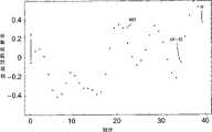
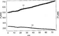
现在转到图9,相对于时间绘出了顶层厚度p1802和沟槽深度p2804。注意到,由于蚀刻工艺随着时间步长t的进行,如应该预期的,沟槽深度p2804增加,而顶层厚度p1802减小。在每个时间步长t计算的参数对独立于先前的值,因此在这些曲线图中看到的平滑的变化表明搜索确实返回了正确值,因为每个值在时间步长之间平滑地转变。图10示出硅中的沟槽深度p41002在相同时间间隔上的曲线图。回想起深度p4是从厚度p1802和深度p2804以及中间层108的已知厚度得到的,很明显硅深度p4的值也是正确的,因为它们在时间步长之间也是从一个值平滑地转变到另一个值。Turning now to FIG. 9 , the top layer thickness p1 802 and trench depth p2 804 are plotted against time. Note that as the etch process proceeds with time step t, trench depthp2 804 increases, while top layer thicknessp1 802 decreases, as should be expected. The parameter pairs computed at each time step t are independent of previous values, so the smooth changes seen in these plots indicate that the search indeed returned the correct values, as each value transitions smoothly between time steps . FIG. 10 shows a graph of trench depth p4 1002 in silicon over the same time interval. Recalling that the depth p4 is obtained from the thickness p1 802 and the depth p2 804 and the known thickness of the
下面的权利要求书中的所有装置或步骤加功能单元的相应结构、材料、运作(act)及等价物旨在包括用于与其它主张权利的单元结合来执行功能的任何结构、材料、或者运作,如具体申明的。为了描述和说明的目的已经陈述了本发明的说明书,但是不想无遗漏地介绍本发明或者局限于公开形式的发明。在不脱离本发明的范围和精神的情况下,许多修改和变化对于本领域的普通技术人员将是显而易见的。选择并且介绍了实施例,以便最好地解释本发明的原理和实际应用,并且是为了当适宜于想要的特定用途时,使本领域的其他普通技术人员能够理解本发明的具有各种修改的各种实施例。本领域的技术人员做出了前面的实施例,并且可以做出各种修改。The corresponding structures, materials, acts and equivalents of all means or step plus function elements in the claims below are intended to include any structure, material, or act for performing the function in combination with other claimed elements, as specifically stated. The description of the present invention has been presented for purposes of illustration and description, but is not intended to be exhaustive or limited to the invention in the form disclosed. Many modifications and variations will be apparent to those of ordinary skill in the art without departing from the scope and spirit of the invention. The embodiment was chosen and described in order to best explain the principles of the invention and the practical application, and to enable others skilled in the art to understand the invention with various modifications as are suited to the particular use contemplated. various embodiments. Those skilled in the art have made the foregoing embodiments and can make various modifications.
Claims (36)
Applications Claiming Priority (3)
| Application Number | Priority Date | Filing Date | Title |
|---|---|---|---|
| US10/392,991 | 2003-03-19 | ||
| US10/392,991US7049156B2 (en) | 2003-03-19 | 2003-03-19 | System and method for in-situ monitor and control of film thickness and trench depth |
| PCT/US2004/007118WO2004086068A1 (en) | 2003-03-19 | 2004-03-09 | System and method for in-situ monitor and control of film thickness and trench depth |
Publications (2)
| Publication Number | Publication Date |
|---|---|
| CN1774639Atrue CN1774639A (en) | 2006-05-17 |
| CN1774639B CN1774639B (en) | 2010-12-15 |
Family
ID=32988016
Family Applications (1)
| Application Number | Title | Priority Date | Filing Date |
|---|---|---|---|
| CN2004800103568AExpired - LifetimeCN1774639B (en) | 2003-03-19 | 2004-03-09 | Method for determining a value of at least one parameter associated with a wafer |
Country Status (9)
| Country | Link |
|---|---|
| US (1) | US7049156B2 (en) |
| EP (1) | EP1611447B1 (en) |
| JP (2) | JP4958546B2 (en) |
| KR (1) | KR100782192B1 (en) |
| CN (1) | CN1774639B (en) |
| AT (1) | ATE497160T1 (en) |
| DE (1) | DE602004031201D1 (en) |
| TW (1) | TWI287080B (en) |
| WO (1) | WO2004086068A1 (en) |
Cited By (7)
| Publication number | Priority date | Publication date | Assignee | Title |
|---|---|---|---|---|
| CN104022049A (en)* | 2013-02-13 | 2014-09-03 | 三星电子株式会社 | Method of calibrating target values and processing systems configured to calibrate target values |
| CN111446179A (en)* | 2020-03-31 | 2020-07-24 | 中国科学院微电子研究所 | Method and device for testing wafers |
| CN111982007A (en)* | 2020-08-27 | 2020-11-24 | 天津大学 | Contrast spectrum system and measurement method for realizing depth measurement of micro groove with high depth-to-width ratio |
| CN115552537A (en)* | 2021-04-13 | 2022-12-30 | 真实仪器公司 | Systems, devices, and methods for spectral filtering |
| CN115579304A (en)* | 2022-11-09 | 2023-01-06 | 广州粤芯半导体技术有限公司 | Wafer detection method and device, computer equipment and readable storage medium |
| CN116482143A (en)* | 2022-01-14 | 2023-07-25 | 长鑫存储技术有限公司 | Wafer measurement system, control method, equipment and medium |
| CN120064120A (en)* | 2025-02-24 | 2025-05-30 | 武汉市莫雷光电科技有限公司 | Blind hole adhesive residue detection device and detection method |
Families Citing this family (59)
| Publication number | Priority date | Publication date | Assignee | Title |
|---|---|---|---|---|
| US7869057B2 (en) | 2002-09-09 | 2011-01-11 | Zygo Corporation | Multiple-angle multiple-wavelength interferometer using high-NA imaging and spectral analysis |
| US7139081B2 (en)* | 2002-09-09 | 2006-11-21 | Zygo Corporation | Interferometry method for ellipsometry, reflectometry, and scatterometry measurements, including characterization of thin film structures |
| US8564780B2 (en) | 2003-01-16 | 2013-10-22 | Jordan Valley Semiconductors Ltd. | Method and system for using reflectometry below deep ultra-violet (DUV) wavelengths for measuring properties of diffracting or scattering structures on substrate work pieces |
| US20080246951A1 (en)* | 2007-04-09 | 2008-10-09 | Phillip Walsh | Method and system for using reflectometry below deep ultra-violet (DUV) wavelengths for measuring properties of diffracting or scattering structures on substrate work-pieces |
| US7324214B2 (en) | 2003-03-06 | 2008-01-29 | Zygo Corporation | Interferometer and method for measuring characteristics of optically unresolved surface features |
| US7106454B2 (en)* | 2003-03-06 | 2006-09-12 | Zygo Corporation | Profiling complex surface structures using scanning interferometry |
| US7271918B2 (en)* | 2003-03-06 | 2007-09-18 | Zygo Corporation | Profiling complex surface structures using scanning interferometry |
| US6999180B1 (en)* | 2003-04-02 | 2006-02-14 | Kla-Tencor Technologies Corporation | Optical film topography and thickness measurement |
| US7298494B2 (en) | 2003-09-15 | 2007-11-20 | Zygo Corporation | Methods and systems for interferometric analysis of surfaces and related applications |
| KR101006422B1 (en) | 2005-01-20 | 2011-01-06 | 지고 코포레이션 | Interferometer to determine the characteristics of the object surface |
| US7884947B2 (en) | 2005-01-20 | 2011-02-08 | Zygo Corporation | Interferometry for determining characteristics of an object surface, with spatially coherent illumination |
| EP1883781B1 (en)* | 2005-05-19 | 2019-08-07 | Zygo Corporation | Analyzing low-coherence interferometry signals for thin film structures |
| US8392012B2 (en)* | 2008-10-27 | 2013-03-05 | Applied Materials, Inc. | Multiple libraries for spectrographic monitoring of zones of a substrate during processing |
| US7636168B2 (en) | 2005-10-11 | 2009-12-22 | Zygo Corporation | Interferometry method and system including spectral decomposition |
| TWI428559B (en) | 2006-07-21 | 2014-03-01 | Zygo Corp | Compensation of systematic effects in low coherence interferometry |
| US20080129986A1 (en)* | 2006-11-30 | 2008-06-05 | Phillip Walsh | Method and apparatus for optically measuring periodic structures using orthogonal azimuthal sample orientations |
| WO2008080127A2 (en) | 2006-12-22 | 2008-07-03 | Zygo Corporation | Apparatus and method for measuring characteristics of surface features |
| US7889355B2 (en) | 2007-01-31 | 2011-02-15 | Zygo Corporation | Interferometry for lateral metrology |
| US7952708B2 (en) | 2007-04-02 | 2011-05-31 | Applied Materials, Inc. | High throughput measurement system |
| TWI416096B (en) | 2007-07-11 | 2013-11-21 | Nova Measuring Instr Ltd | Method and system for use in monitoring properties of patterned structures |
| US7619746B2 (en) | 2007-07-19 | 2009-11-17 | Zygo Corporation | Generating model signals for interferometry |
| US20090065478A1 (en)* | 2007-09-11 | 2009-03-12 | Dockery Kevin P | Measuring etching rates using low coherence interferometry |
| US7761179B2 (en)* | 2007-09-24 | 2010-07-20 | Intel Corporation | Method for consistent updates to automated process control (APC) models with partitioning along multiple components |
| US8072611B2 (en) | 2007-10-12 | 2011-12-06 | Zygo Corporation | Interferometric analysis of under-resolved features |
| US8327191B2 (en) | 2007-10-19 | 2012-12-04 | International Business Machines Corporation | Automatically populating symptom databases for software applications |
| KR101274517B1 (en) | 2007-11-13 | 2013-06-13 | 지고 코포레이션 | Interferometer utilizing polarization scanning |
| EP2232195B1 (en) | 2007-12-14 | 2015-03-18 | Zygo Corporation | Analyzing surface structure using scanning interferometry |
| KR100897109B1 (en)* | 2008-01-25 | 2009-05-14 | 메트로솔 인코포레이티드 | Vacuum ultraviolet reference reflectometer |
| US8760649B1 (en) | 2008-01-28 | 2014-06-24 | Kla-Tencor Corporation | Model-based metrology using tesselation-based discretization |
| US20090275265A1 (en)* | 2008-05-02 | 2009-11-05 | Applied Materials, Inc. | Endpoint detection in chemical mechanical polishing using multiple spectra |
| US8004688B2 (en) | 2008-11-26 | 2011-08-23 | Zygo Corporation | Scan error correction in low coherence scanning interferometry |
| CN103119704A (en) | 2010-07-23 | 2013-05-22 | 第一太阳能有限公司 | In-line metrology system and method |
| US8954186B2 (en) | 2010-07-30 | 2015-02-10 | Applied Materials, Inc. | Selecting reference libraries for monitoring of multiple zones on a substrate |
| US8892568B2 (en)* | 2010-10-15 | 2014-11-18 | Applied Materials, Inc. | Building a library of spectra for optical monitoring |
| US8666530B2 (en) | 2010-12-16 | 2014-03-04 | Electro Scientific Industries, Inc. | Silicon etching control method and system |
| US8867041B2 (en) | 2011-01-18 | 2014-10-21 | Jordan Valley Semiconductor Ltd | Optical vacuum ultra-violet wavelength nanoimprint metrology |
| US8565379B2 (en) | 2011-03-14 | 2013-10-22 | Jordan Valley Semiconductors Ltd. | Combining X-ray and VUV analysis of thin film layers |
| GB2489722B (en) | 2011-04-06 | 2017-01-18 | Precitec Optronik Gmbh | Apparatus and method for determining a depth of a region having a high aspect ratio that protrudes into a surface of a semiconductor wafer |
| CN102420152A (en)* | 2011-04-29 | 2012-04-18 | 上海华力微电子有限公司 | Method for controlling thickness of surplus silicon oxide in groove of power device in on-line manner |
| DE102011051146B3 (en) | 2011-06-17 | 2012-10-04 | Precitec Optronik Gmbh | Test method for testing a bonding layer between wafer-shaped samples |
| KR101892914B1 (en) | 2012-03-08 | 2018-08-29 | 어플라이드 머티어리얼스, 인코포레이티드 | Fitting of optical model to measured spectrum |
| CN104395690B (en)* | 2012-06-13 | 2017-05-31 | 株式会社新柯隆 | Film thickness measurement device and film formation device |
| US9248544B2 (en)* | 2012-07-18 | 2016-02-02 | Applied Materials, Inc. | Endpoint detection during polishing using integrated differential intensity |
| DE102012111008B4 (en) | 2012-11-15 | 2014-05-22 | Precitec Optronik Gmbh | Optical measuring method and optical measuring device for detecting a surface topography |
| KR101882591B1 (en) | 2013-06-17 | 2018-08-24 | 프레시텍 옵트로닉 게엠베하 | Optical measuring device for recording differences in distance and optical measuring method |
| US10955359B2 (en)* | 2013-11-12 | 2021-03-23 | International Business Machines Corporation | Method for quantification of process non uniformity using model-based metrology |
| US10234265B2 (en) | 2016-12-12 | 2019-03-19 | Precitec Optronik Gmbh | Distance measuring device and method for measuring distances |
| US10861755B2 (en) | 2017-02-08 | 2020-12-08 | Verity Instruments, Inc. | System and method for measurement of complex structures |
| US11424115B2 (en)* | 2017-03-31 | 2022-08-23 | Verity Instruments, Inc. | Multimode configurable spectrometer |
| DE102017126310A1 (en) | 2017-11-09 | 2019-05-09 | Precitec Optronik Gmbh | Distance measuring device |
| DE102018130901A1 (en) | 2018-12-04 | 2020-06-04 | Precitec Optronik Gmbh | Optical measuring device |
| KR102786800B1 (en) | 2019-05-20 | 2025-03-25 | 삼성전자주식회사 | Apparatus and method for determining validity of bio-information estimation model |
| DE102020100565A1 (en) | 2020-01-13 | 2021-07-15 | Aixtron Se | Process for depositing layers |
| KR102825817B1 (en) | 2020-08-28 | 2025-06-30 | 삼성전자주식회사 | Thickness estimation method and process control method |
| US12218015B2 (en)* | 2021-04-16 | 2025-02-04 | Taiwan Semiconductor Manufacturing Company, Ltd. | Interferometer systems and methods for real time etch process compensation control |
| US12165936B2 (en) | 2021-07-08 | 2024-12-10 | Taiwan Semiconductor Manufacturing Co., Ltd. | End point control in etching processes |
| KR20230092176A (en) | 2021-12-17 | 2023-06-26 | 삼성전자주식회사 | Device for radical diagonostic in plasma process chamber, radical diagonostic systemt having the same, and operating method thereof |
| EP4235469A1 (en)* | 2022-02-25 | 2023-08-30 | Commissariat À L'Énergie Atomique Et Aux Énergies Alternatives | A system for detecting malwares in a resources constrained device |
| US12174071B2 (en) | 2022-05-13 | 2024-12-24 | Verity Instruments, Inc. | System, apparatus, and method for improved background correction and calibration of optical devices |
Family Cites Families (21)
| Publication number | Priority date | Publication date | Assignee | Title |
|---|---|---|---|---|
| JPH0617774B2 (en)* | 1987-06-22 | 1994-03-09 | 大日本スクリ−ン製造株式会社 | Micro height difference measuring device |
| US4807994A (en)* | 1987-11-19 | 1989-02-28 | Varian Associates, Inc. | Method of mapping ion implant dose uniformity |
| US5392118A (en)* | 1992-05-13 | 1995-02-21 | International Business Machines Corporation | Method for measuring a trench depth parameter of a material |
| US5365340A (en)* | 1992-12-10 | 1994-11-15 | Hughes Aircraft Company | Apparatus and method for measuring the thickness of thin films |
| JPH074922A (en)* | 1993-06-21 | 1995-01-10 | Jasco Corp | Semiconductor multilayer thin film thickness measuring apparatus and its measuring method |
| US5555472A (en)* | 1993-12-22 | 1996-09-10 | Integrated Process Equipment Corp. | Method and apparatus for measuring film thickness in multilayer thin film stack by comparison to a reference library of theoretical signatures |
| JP3670336B2 (en)* | 1995-03-27 | 2005-07-13 | 富士通株式会社 | Silicon oxide film evaluation method and semiconductor device manufacturing method |
| JPH0961344A (en)* | 1995-08-24 | 1997-03-07 | Dainippon Screen Mfg Co Ltd | Surface treatment end point detecting method |
| JPH10209039A (en)* | 1997-01-27 | 1998-08-07 | Nikon Corp | Projection exposure method and projection exposure apparatus |
| JPH1114312A (en)* | 1997-06-24 | 1999-01-22 | Toshiba Corp | Film forming apparatus and etching apparatus |
| US5900633A (en)* | 1997-12-15 | 1999-05-04 | On-Line Technologies, Inc | Spectrometric method for analysis of film thickness and composition on a patterned sample |
| US6048742A (en)* | 1998-02-26 | 2000-04-11 | The United States Of America As Represented By The Secretary Of The Air Force | Process for measuring the thickness and composition of thin semiconductor films deposited on semiconductor wafers |
| IL123727A (en)* | 1998-03-18 | 2002-05-23 | Nova Measuring Instr Ltd | Method and apparatus for measurement of patterned structures |
| US6106662A (en)* | 1998-06-08 | 2000-08-22 | Speedfam-Ipec Corporation | Method and apparatus for endpoint detection for chemical mechanical polishing |
| US6275297B1 (en)* | 1998-08-19 | 2001-08-14 | Sc Technology | Method of measuring depths of structures on a semiconductor substrate |
| DE19852323C2 (en)* | 1998-11-12 | 2001-08-16 | Steag Hamatech Ag | Method for determining the thickness of layers provided on a substrate |
| JP2000205833A (en)* | 1999-01-06 | 2000-07-28 | Internatl Business Mach Corp <Ibm> | Non-destructive method and apparatus for measuring depth of recessed material |
| TW507305B (en)* | 1999-09-18 | 2002-10-21 | Samsung Electronics Co Ltd | Method of measuring etched state of semiconductor wafer |
| JP2001099622A (en)* | 1999-09-29 | 2001-04-13 | Toshiba Corp | Depth measuring device and depth measuring method |
| US6491569B2 (en)* | 2001-04-19 | 2002-12-10 | Speedfam-Ipec Corporation | Method and apparatus for using optical reflection data to obtain a continuous predictive signal during CMP |
| CN1187600C (en)* | 2002-10-31 | 2005-02-02 | 中国科学院上海技术物理研究所 | Apparatus and method for measuring equivalent refraction power of optical film and physical thickness |
- 2003
- 2003-03-19USUS10/392,991patent/US7049156B2/ennot_activeExpired - Lifetime
- 2004
- 2004-03-09DEDE602004031201Tpatent/DE602004031201D1/ennot_activeExpired - Lifetime
- 2004-03-09JPJP2006506975Apatent/JP4958546B2/ennot_activeExpired - Lifetime
- 2004-03-09EPEP04718815Apatent/EP1611447B1/ennot_activeExpired - Lifetime
- 2004-03-09WOPCT/US2004/007118patent/WO2004086068A1/enactiveApplication Filing
- 2004-03-09CNCN2004800103568Apatent/CN1774639B/ennot_activeExpired - Lifetime
- 2004-03-09KRKR1020057017362Apatent/KR100782192B1/ennot_activeExpired - Fee Related
- 2004-03-09ATAT04718815Tpatent/ATE497160T1/ennot_activeIP Right Cessation
- 2004-03-19TWTW093107542Apatent/TWI287080B/ennot_activeIP Right Cessation
- 2009
- 2009-12-21JPJP2009289774Apatent/JP2010199557A/enactivePending
Cited By (10)
| Publication number | Priority date | Publication date | Assignee | Title |
|---|---|---|---|---|
| CN104022049A (en)* | 2013-02-13 | 2014-09-03 | 三星电子株式会社 | Method of calibrating target values and processing systems configured to calibrate target values |
| CN104022049B (en)* | 2013-02-13 | 2018-05-25 | 三星电子株式会社 | It calibrates the method for desired value and is configured to the processing system of calibration desired value |
| CN111446179A (en)* | 2020-03-31 | 2020-07-24 | 中国科学院微电子研究所 | Method and device for testing wafers |
| CN111446179B (en)* | 2020-03-31 | 2022-11-01 | 中国科学院微电子研究所 | Method and device for testing wafers |
| CN111982007A (en)* | 2020-08-27 | 2020-11-24 | 天津大学 | Contrast spectrum system and measurement method for realizing depth measurement of micro groove with high depth-to-width ratio |
| CN115552537A (en)* | 2021-04-13 | 2022-12-30 | 真实仪器公司 | Systems, devices, and methods for spectral filtering |
| CN115552537B (en)* | 2021-04-13 | 2024-03-19 | 真实仪器公司 | Systems, devices and methods for spectral filtering |
| CN116482143A (en)* | 2022-01-14 | 2023-07-25 | 长鑫存储技术有限公司 | Wafer measurement system, control method, equipment and medium |
| CN115579304A (en)* | 2022-11-09 | 2023-01-06 | 广州粤芯半导体技术有限公司 | Wafer detection method and device, computer equipment and readable storage medium |
| CN120064120A (en)* | 2025-02-24 | 2025-05-30 | 武汉市莫雷光电科技有限公司 | Blind hole adhesive residue detection device and detection method |
Also Published As
| Publication number | Publication date |
|---|---|
| JP2010199557A (en) | 2010-09-09 |
| KR100782192B1 (en) | 2007-12-04 |
| WO2004086068A1 (en) | 2004-10-07 |
| JP2006521014A (en) | 2006-09-14 |
| US20040185582A1 (en) | 2004-09-23 |
| EP1611447A4 (en) | 2009-11-11 |
| US7049156B2 (en) | 2006-05-23 |
| EP1611447B1 (en) | 2011-01-26 |
| ATE497160T1 (en) | 2011-02-15 |
| CN1774639B (en) | 2010-12-15 |
| TWI287080B (en) | 2007-09-21 |
| DE602004031201D1 (en) | 2011-03-10 |
| KR20050110011A (en) | 2005-11-22 |
| JP4958546B2 (en) | 2012-06-20 |
| TW200422589A (en) | 2004-11-01 |
| EP1611447A1 (en) | 2006-01-04 |
Similar Documents
| Publication | Publication Date | Title |
|---|---|---|
| CN1774639B (en) | Method for determining a value of at least one parameter associated with a wafer | |
| US7826071B2 (en) | Parametric profiling using optical spectroscopic systems | |
| CN113167744B (en) | Scattering measurement-based method and system for strain measurement in semiconductor structures | |
| US6485872B1 (en) | Method and apparatus for measuring the composition and other properties of thin films utilizing infrared radiation | |
| JP5102329B2 (en) | Measurement of diffractive structures, broadband, polarization, ellipsometry and underlying structures | |
| TWI603052B (en) | Method, system, and computer-readable medium to generate optimized measurement recipe | |
| US20130245985A1 (en) | Calibration Of An Optical Metrology System For Critical Dimension Application Matching | |
| KR101656436B1 (en) | Method for measuring film thickness distribution of wafer having thin film | |
| US7327475B1 (en) | Measuring a process parameter of a semiconductor fabrication process using optical metrology | |
| US20020113966A1 (en) | Parametric profiling using optical spectroscopic systems | |
| TW200403785A (en) | Method for in-situ monitoring of patterned substrate processing using reflectometry | |
| US9243886B1 (en) | Optical metrology of periodic targets in presence of multiple diffraction orders | |
| JP2009536354A (en) | A method and apparatus for precisely calibrating a reflectometer using a specific reflectivity measurement method | |
| US7839509B2 (en) | Method of measuring deep trenches with model-based optical spectroscopy | |
| US7773232B2 (en) | Apparatus and method for determining trench parameters | |
| US20240053280A1 (en) | Methods And Systems For Systematic Error Compensation Across A Fleet Of Metrology Systems Based On A Trained Error Evaluation Model | |
| US6472238B1 (en) | Evaluation of etching processes in semiconductors | |
| US6605482B2 (en) | Process for monitoring the thickness of layers in a microelectronic device | |
| CN117685899A (en) | Method for measuring pattern structure morphology parameters | |
| TWI452283B (en) | A method of calibrating a system that obtains reflectance data and a method of calibrating a reflectometer | |
| TW202534814A (en) | Methods and systems for reflectometry based measurements of deep, large pitch semiconductor structures | |
| Hu et al. | Measurements of shallow trench isolation by normal incidence optical critical dimension technique | |
| Venugopal et al. | Manufacturability considerations in designing optical monitoring methods for control of plasma etch processes | |
| Galarza et al. | Analysis of time-evolved spectroscopic ellipsometry data from patterned structures for etching process monitoring and control |
Legal Events
| Date | Code | Title | Description |
|---|---|---|---|
| C06 | Publication | ||
| PB01 | Publication | ||
| C10 | Entry into substantive examination | ||
| SE01 | Entry into force of request for substantive examination | ||
| C14 | Grant of patent or utility model | ||
| GR01 | Patent grant | ||
| C56 | Change in the name or address of the patentee | ||
| CP01 | Change in the name or title of a patent holder | Address after:Texas, USA Patentee after:VERITY INSTRUMENTS, Inc. Address before:Texas, USA Patentee before:Verity Instruments, Inc. | |
| C56 | Change in the name or address of the patentee | ||
| CP02 | Change in the address of a patent holder | Address after:Texas, USA Patentee after:VERITY INSTRUMENTS, Inc. Address before:Texas, USA Patentee before:VERITY INSTRUMENTS, Inc. | |
| CX01 | Expiry of patent term | Granted publication date:20101215 | |
| CX01 | Expiry of patent term |