CN1763968A - Bipolar device and method of increasing charge carrier mobility therein - Google Patents
Bipolar device and method of increasing charge carrier mobility thereinDownload PDFInfo
- Publication number
- CN1763968A CN1763968ACNA2005100978284ACN200510097828ACN1763968ACN 1763968 ACN1763968 ACN 1763968ACN A2005100978284 ACNA2005100978284 ACN A2005100978284ACN 200510097828 ACN200510097828 ACN 200510097828ACN 1763968 ACN1763968 ACN 1763968A
- Authority
- CN
- China
- Prior art keywords
- intrinsic base
- base stage
- sige
- bipolar device
- stressor layers
- Prior art date
- Legal status (The legal status is an assumption and is not a legal conclusion. Google has not performed a legal analysis and makes no representation as to the accuracy of the status listed.)
- Granted
Links
- 238000000034methodMethods0.000titleclaimsabstractdescription27
- 230000001965increasing effectEffects0.000titleclaimsabstractdescription25
- 239000002800charge carrierSubstances0.000titleclaimsabstractdescription6
- 229910000577Silicon-germaniumInorganic materials0.000claimsdescription53
- 229910052710siliconInorganic materials0.000claimsdescription29
- 239000010703siliconSubstances0.000claimsdescription29
- 239000000463materialSubstances0.000claimsdescription20
- 230000006835compressionEffects0.000claimsdescription10
- 238000007906compressionMethods0.000claimsdescription10
- 229910010271silicon carbideInorganic materials0.000claimsdescription9
- 230000037230mobilityEffects0.000description35
- XUIMIQQOPSSXEZ-UHFFFAOYSA-NSiliconChemical compound[Si]XUIMIQQOPSSXEZ-UHFFFAOYSA-N0.000description23
- 230000007935neutral effectEffects0.000description18
- 229910021420polycrystalline siliconInorganic materials0.000description14
- 229920005591polysiliconPolymers0.000description14
- 239000010408filmSubstances0.000description13
- 150000004767nitridesChemical class0.000description11
- 230000008901benefitEffects0.000description10
- 239000000969carrierSubstances0.000description10
- 239000004065semiconductorSubstances0.000description10
- VYPSYNLAJGMNEJ-UHFFFAOYSA-NSilicium dioxideChemical compoundO=[Si]=OVYPSYNLAJGMNEJ-UHFFFAOYSA-N0.000description8
- LEVVHYCKPQWKOP-UHFFFAOYSA-N[Si].[Ge]Chemical compound[Si].[Ge]LEVVHYCKPQWKOP-UHFFFAOYSA-N0.000description8
- 238000000151depositionMethods0.000description7
- 125000006850spacer groupChemical group0.000description7
- 239000012535impuritySubstances0.000description6
- 238000002955isolationMethods0.000description6
- 229910021332silicideInorganic materials0.000description5
- 238000001020plasma etchingMethods0.000description4
- FVBUAEGBCNSCDD-UHFFFAOYSA-Nsilicide(4-)Chemical compound[Si-4]FVBUAEGBCNSCDD-UHFFFAOYSA-N0.000description4
- HBMJWWWQQXIZIP-UHFFFAOYSA-Nsilicon carbideChemical compound[Si+]#[C-]HBMJWWWQQXIZIP-UHFFFAOYSA-N0.000description4
- 239000000377silicon dioxideSubstances0.000description4
- 239000000758substrateSubstances0.000description4
- ZOXJGFHDIHLPTG-UHFFFAOYSA-NBoronChemical compound[B]ZOXJGFHDIHLPTG-UHFFFAOYSA-N0.000description3
- 229910052796boronInorganic materials0.000description3
- 230000008021depositionEffects0.000description3
- 238000009792diffusion processMethods0.000description3
- 239000002019doping agentSubstances0.000description3
- 238000005516engineering processMethods0.000description3
- 238000005530etchingMethods0.000description3
- 229910052732germaniumInorganic materials0.000description3
- GNPVGFCGXDBREM-UHFFFAOYSA-Ngermanium atomChemical compound[Ge]GNPVGFCGXDBREM-UHFFFAOYSA-N0.000description3
- 239000012212insulatorSubstances0.000description3
- 238000004519manufacturing processMethods0.000description3
- 238000000206photolithographyMethods0.000description3
- 235000012239silicon dioxideNutrition0.000description3
- 238000004088simulationMethods0.000description3
- 239000000126substanceSubstances0.000description3
- OAICVXFJPJFONN-UHFFFAOYSA-NPhosphorusChemical compound[P]OAICVXFJPJFONN-UHFFFAOYSA-N0.000description2
- 229910052581Si3N4Inorganic materials0.000description2
- 238000006243chemical reactionMethods0.000description2
- 238000011161developmentMethods0.000description2
- 238000000407epitaxyMethods0.000description2
- 238000001451molecular beam epitaxyMethods0.000description2
- 229910052698phosphorusInorganic materials0.000description2
- 239000011574phosphorusSubstances0.000description2
- 238000012545processingMethods0.000description2
- 238000001289rapid thermal chemical vapour depositionMethods0.000description2
- 229910045601alloyInorganic materials0.000description1
- 239000000956alloySubstances0.000description1
- 229910052787antimonyInorganic materials0.000description1
- WATWJIUSRGPENY-UHFFFAOYSA-Nantimony atomChemical compound[Sb]WATWJIUSRGPENY-UHFFFAOYSA-N0.000description1
- 238000013459approachMethods0.000description1
- 229910052785arsenicInorganic materials0.000description1
- RQNWIZPPADIBDY-UHFFFAOYSA-Narsenic atomChemical compound[As]RQNWIZPPADIBDY-UHFFFAOYSA-N0.000description1
- 238000010420art techniqueMethods0.000description1
- 238000005229chemical vapour depositionMethods0.000description1
- 229910052681coesiteInorganic materials0.000description1
- 229910052906cristobaliteInorganic materials0.000description1
- 230000000694effectsEffects0.000description1
- 230000002708enhancing effectEffects0.000description1
- 230000005669field effectEffects0.000description1
- 125000005842heteroatomChemical group0.000description1
- 230000001939inductive effectEffects0.000description1
- 229910052751metalInorganic materials0.000description1
- 239000002184metalSubstances0.000description1
- 239000000203mixtureSubstances0.000description1
- 229910021421monocrystalline siliconInorganic materials0.000description1
- 230000003071parasitic effectEffects0.000description1
- 238000005389semiconductor device fabricationMethods0.000description1
- HQVNEWCFYHHQES-UHFFFAOYSA-Nsilicon nitrideChemical compoundN12[Si]34N5[Si]62N3[Si]51N64HQVNEWCFYHHQES-UHFFFAOYSA-N0.000description1
- 239000007787solidSubstances0.000description1
- 238000004544sputter depositionMethods0.000description1
- 229910052682stishoviteInorganic materials0.000description1
- 238000006467substitution reactionMethods0.000description1
- 239000010409thin filmSubstances0.000description1
- 238000012546transferMethods0.000description1
- 229910052905tridymiteInorganic materials0.000description1
- 238000001039wet etchingMethods0.000description1
Images


Classifications
- H—ELECTRICITY
- H10—SEMICONDUCTOR DEVICES; ELECTRIC SOLID-STATE DEVICES NOT OTHERWISE PROVIDED FOR
- H10D—INORGANIC ELECTRIC SEMICONDUCTOR DEVICES
- H10D10/00—Bipolar junction transistors [BJT]
- H10D10/01—Manufacture or treatment
- H10D10/021—Manufacture or treatment of heterojunction BJTs [HBT]
- H—ELECTRICITY
- H10—SEMICONDUCTOR DEVICES; ELECTRIC SOLID-STATE DEVICES NOT OTHERWISE PROVIDED FOR
- H10D—INORGANIC ELECTRIC SEMICONDUCTOR DEVICES
- H10D10/00—Bipolar junction transistors [BJT]
- H10D10/80—Heterojunction BJTs
- H10D10/821—Vertical heterojunction BJTs
- H10D10/891—Vertical heterojunction BJTs comprising lattice-mismatched active layers, e.g. SiGe strained-layer transistors
- H—ELECTRICITY
- H10—SEMICONDUCTOR DEVICES; ELECTRIC SOLID-STATE DEVICES NOT OTHERWISE PROVIDED FOR
- H10D—INORGANIC ELECTRIC SEMICONDUCTOR DEVICES
- H10D62/00—Semiconductor bodies, or regions thereof, of devices having potential barriers
- H10D62/80—Semiconductor bodies, or regions thereof, of devices having potential barriers characterised by the materials
- H10D62/871—Semiconductor bodies, or regions thereof, of devices having potential barriers characterised by the materials being Group I-VI materials, e.g. Cu2O; being Group I-VII materials, e.g. CuI
- H—ELECTRICITY
- H10—SEMICONDUCTOR DEVICES; ELECTRIC SOLID-STATE DEVICES NOT OTHERWISE PROVIDED FOR
- H10D—INORGANIC ELECTRIC SEMICONDUCTOR DEVICES
- H10D84/00—Integrated devices formed in or on semiconductor substrates that comprise only semiconducting layers, e.g. on Si wafers or on GaAs-on-Si wafers
- H10D84/01—Manufacture or treatment
- H10D84/0107—Integrating at least one component covered by H10D12/00 or H10D30/00 with at least one component covered by H10D8/00, H10D10/00 or H10D18/00, e.g. integrating IGFETs with BJTs
- H10D84/0109—Integrating at least one component covered by H10D12/00 or H10D30/00 with at least one component covered by H10D8/00, H10D10/00 or H10D18/00, e.g. integrating IGFETs with BJTs the at least one component covered by H10D12/00 or H10D30/00 being a MOS device
- H—ELECTRICITY
- H10—SEMICONDUCTOR DEVICES; ELECTRIC SOLID-STATE DEVICES NOT OTHERWISE PROVIDED FOR
- H10D—INORGANIC ELECTRIC SEMICONDUCTOR DEVICES
- H10D84/00—Integrated devices formed in or on semiconductor substrates that comprise only semiconducting layers, e.g. on Si wafers or on GaAs-on-Si wafers
- H10D84/01—Manufacture or treatment
- H10D84/02—Manufacture or treatment characterised by using material-based technologies
- H10D84/03—Manufacture or treatment characterised by using material-based technologies using Group IV technology, e.g. silicon technology or silicon-carbide [SiC] technology
- H10D84/038—Manufacture or treatment characterised by using material-based technologies using Group IV technology, e.g. silicon technology or silicon-carbide [SiC] technology using silicon technology, e.g. SiGe
Landscapes
- Bipolar Transistors (AREA)
Abstract
Translated fromChineseDescription
Translated fromChinese技术领域technical field
本发明涉及半导体器件制造,更具体地,是涉及用于提高双极型器件的性能的技术。The present invention relates to semiconductor device fabrication and, more particularly, to techniques for improving the performance of bipolar devices.
背景技术Background technique
双极型器件是一种半导体器件,其工作是以同时使用多数载流子和少数载流子(也称作“电荷载流子”)为基础。多数载流子和少数载流子根据器件的极性或者是电子或者是空穴。A bipolar device is a semiconductor device whose operation is based on the simultaneous use of majority and minority carriers (also called "charge carriers"). The majority and minority carriers are either electrons or holes depending on the polarity of the device.
一种双极型器件的例子是双极结晶体管(BJT),其是具有称作发射极、基极和集电极的三个半导体区的晶体管。发射极是具有非常高的导电率的区域,用作被注入到临近的基极的自由载流子的源。集电极是收集来自基极的载流子的区域。基极区夹在发射区与集电区之间,通常控制发射极与集电极之间的自由载流子的流动。与从发射极流到集电极的载流子极性相反的较小的载流子流从基极流到发射极。An example of a bipolar device is a bipolar junction transistor (BJT), which is a transistor having three semiconductor regions called emitter, base and collector. The emitter is a region of very high conductivity that acts as a source of free carriers that are injected into the adjacent base. The collector is the region where the carriers from the base are collected. The base region is sandwiched between the emitter and collector regions and normally controls the flow of free carriers between the emitter and collector. A flow of smaller carriers of opposite polarity to the carriers flowing from the emitter to the collector flows from the base to the emitter.
传统的BJT是使用一种具有不同掺杂区的半导体材料(Si)来制造的。异质结双极型晶体管(HBT)使用多于一种的半导体材料(利用不同材料的不同特性如带隙),例如与Si组合的SiGe。其它的材料(除了Si以外)通常使用MBE(分子束外延)、RTCVD(快速热化学气相淀积)或LPCVD(低温化学气相淀积)技术而作为外延层形成。Traditional BJTs are fabricated using a semiconductor material (Si) with differently doped regions. Heterojunction bipolar transistors (HBT) use more than one semiconductor material (taking advantage of different properties of different materials such as bandgap), eg SiGe combined with Si. Other materials (other than Si) are usually formed as epitaxial layers using MBE (Molecular Beam Epitaxy), RTCVD (Rapid Thermal Chemical Vapor Deposition) or LPCVD (Low Temperature Chemical Vapor Deposition) techniques.
双极型晶体管包括含有第一导电类型的杂质的发射极层(或区)、含有第二导电类型的杂质的基极层(或区)、以及含有第一导电类型的杂质的集电极层(或区)。A bipolar transistor includes an emitter layer (or region) containing impurities of a first conductivity type, a base layer (or region) containing impurities of a second conductivity type, and a collector layer (or regions) containing impurities of a first conductivity type ( or area).
双极型晶体管通常有两种不同的类型或极性——npn(具有n型发射极和集电极以及p型基极)或者pnp(具有p型发射极和集电极以及n型基极)。“类型”(p或n)由外延期间注入或淀积到半导体材料中的杂质而定。用于p型的杂质是硼(B),用于n型的杂质是磷(P)、砷(As)、锑(Sb)。Bipolar transistors generally come in two different types or polarities - npn (with n-type emitter and collector and p-type base) or pnp (with p-type emitter and collector and n-type base). The "type" (p or n) is determined by the impurities implanted or deposited into the semiconductor material during epitaxy. Impurities for p-type are boron (B), and impurities for n-type are phosphorus (P), arsenic (As), and antimony (Sb).
对于npn型双极型晶体管,从发射极注入的自由载流子是电子,从基极流到发射极的载流子是空穴。对于pnp型双极型晶体管,载流子类型相反。通常,将电子而不是空穴称作多数电荷载流子,因为载流子迁移率(μ)μn>μp,饱和速度(V)Vn>Vp。因此,在可能的情况下n型双极型器件通常是优选的。For npn bipolar transistors, the free carriers injected from the emitter are electrons, and the carriers flowing from the base to the emitter are holes. For pnp bipolar transistors, the carrier types are reversed. Typically, electrons rather than holes are referred to as majority charge carriers, since carrier mobility (μ) μn > μp and saturation velocity (V) Vn > Vp . Therefore, n-type bipolar devices are generally preferred where possible.
图1一般性地示出了现有技术的npn型BJT,其包括中性的发射极、中性的集电极和设置在中性发射极与中性集电极之间的中性的基极,示出了电子经由基极从中性的发射极到中性的集电极的通路,并且示出了空穴从中性的基极到中性的发射极的通路。发射极基极空间电荷层(区)形成在中性的发射极与中性的基极之间。基极集电极空间电荷层(区)形成在中性的基极与中性的集电极之间。(对于pnp极性BJT,空穴在中性的发射极与中性的集电极之间移动,电子在中性的基极与中性的发射极之间移动。)Figure 1 generally shows a prior art npn-type BJT comprising a neutral emitter, a neutral collector, and a neutral base disposed between the neutral emitter and neutral collector, The passage of electrons from the neutral emitter to the neutral collector via the base is shown, and the passage of holes from the neutral base to the neutral emitter is shown. An emitter-base space charge layer (region) is formed between a neutral emitter and a neutral base. The base-collector space charge layer (region) is formed between the neutral base and the neutral collector. (For a pnp polarity BJT, holes move between a neutral emitter and a neutral collector, and electrons move between a neutral base and a neutral emitter.)
已知晶格应力影响载流子迁移率和饱和速度。已经显示了各种在场效应晶体管(FET)中导致应力的方法。例如,在电流方向中(有时在垂直于电流方向的方向上)产生张应力的薄膜能够提高FET中的电子迁移率和饱和速度。应当理解,FET工作的基本原理不同于BJT。首先,只在一个方向上有电荷流,其平行于晶片表面。此外,FET具有单一的载流子(对于N型FET为电子,对于P型FET为空穴),晶格应力的应用直向的,以便主要在单一载流子类型的一个方向上产生应力。Lattice stress is known to affect carrier mobility and saturation velocity. Various methods of inducing stress in field effect transistors (FETs) have been shown. For example, thin films that create tensile stress in the direction of current flow (sometimes in a direction perpendicular to the direction of current flow) can increase electron mobility and saturation velocity in FETs. It should be understood that the fundamentals of operation of FETs differ from those of BJTs. First, there is charge flow in only one direction, parallel to the wafer surface. Furthermore, FETs have a single carrier (electrons for N-type FETs, holes for P-type FETs) and the application of lattice stress is vertical so as to induce stress primarily in one direction of the single carrier type.
能够在下面的论文中发现在FET中采用应力技术的一些例子:Some examples of stress techniques employed in FETs can be found in the following papers:
T.Ghani等人的“A 90nm High Volume Manufacturing LogicTechnology Featuring Novel 45nm Gate Length Strained SiliconCMOS Transistors”,英特尔公司Portland Technology Development,希尔巴罗(Hillsboro),俄勒冈州,在2003年3月3日的IEEE+(0-7803-7873)中公开了应变晶体管结构的细节,该晶体管结合了300mm晶片上的90nm逻辑技术。该应变PMOS晶体管结构的特征在于外延生长的埋入在源极区的应变SiGe薄膜。报道了其相对于未应变器件的显著的性能提升。其附图1显示了具有应变外延SiGe薄膜的PMOS晶体管,该外延SiGe薄膜埋入在源极区以在沟道区中产生压缩应变。"A 90nm High Volume Manufacturing Logic Technology Featuring Novel 45nm Gate Length Strained Silicon CMOS Transistors" by T. Ghani et al., Portland Technology Development, Intel Corporation, Hillsboro, Ore., IEEE+( 0-7803-7873) discloses details of the structure of the strained transistor incorporating 90nm logic technology on a 300mm wafer. The strained PMOS transistor structure is characterized by an epitaxially grown strained SiGe film buried in the source region. Significant performance improvements over unstrained devices are reported. Figure 1 thereof shows a PMOS transistor with a strained epitaxial SiGe film buried in the source region to create compressive strain in the channel region.
K.Rim等人的“Enhanced Hole Mobilities in Surface-channelStrained-Si p-MOSFETs”,固体电子实验室(Solid State ElectricsLaboratory),斯坦福大学(Stanford University),斯坦福,加利福尼亚州94305,1995年(c)的IEEE(0-7803-2700-4)中公开了在采用伪晶应变硅层的应变表面沟道p-MOSFETs中空穴迁移率的应变依赖性。观察到了当Ge含量在弛豫Si1-xGex缓冲层中增加时,空穴迁移率的增加随着应变而线性增加。"Enhanced Hole Mobilities in Surface-channel Strained-Si p-MOSFETs" by K. Rim et al., Solid State Electrics Laboratory, Stanford University, Stanford, CA 94305, 1995 (c) The strain dependence of hole mobility in strained surface channel p-MOSFETs employing pseudomorphic strained silicon layers is disclosed in IEEE (0-7803-2700-4). It was observed that the increase in hole mobility increases linearly with strain as the Ge content increases in the relaxed Si1-x Gex buffer layer.
K.Rim等人的“Fabrication and Mobility Characteristics ofUltra-thin Strained Si Directly on Insulator(SSDOI)MOSFETs”,T·J·沃森研究中心(T.J.Watson Research Center),YorktownHeights,纽约10598,IEEE(0-7803-78733/03)中公开了转移拉伸应变硅层,以直接在绝缘体(SSDOI)结构上形成超薄(小于20nm)应变硅。制造MOSFET,根据直接在绝缘体结构上的应变硅证明了电子和空穴迁移率的增加,该绝缘结构在应变硅沟道下没有SiGe层。"Fabrication and Mobility Characteristics of Ultra-thin Strained Si Directly on Insulator (SSDOI) MOSFETs" by K. Rim et al., T.J. Watson Research Center, Yorktown Heights, New York 10598, IEEE (0-7803 - 78733/03) discloses the transfer of tensile strained silicon layers to form ultrathin (less than 20 nm) strained silicon directly on insulator (SSDOI) structures. Fabricated MOSFETs demonstrated increased electron and hole mobility based on strained silicon directly on the insulator structure without a SiGe layer under the strained silicon channel.
发明内容Contents of the invention
电路可从增加晶体管的性能而获益。如上所述,应变的硅晶格可增强MOSFET器件的性能,由此提高这些器件中低场载流子迁移率以及驱动电流。然而,根据发明人的了解,外部应变没有被引入到双极型器件用于增强性能。其中,迄今为止许多方法说明了将应变引入MOSFET器件,但是用于双极型器件的领域仍然未被开发。Circuits can benefit from increased transistor performance. As noted above, strained silicon lattices can enhance the performance of MOSFET devices, thereby increasing low-field carrier mobility and drive current in these devices. However, to the inventors' knowledge, no external strain has been introduced into the bipolar device for performance enhancement. Of these, many approaches have so far demonstrated the introduction of strain into MOSFET devices, but the field for bipolar devices remains unexplored.
双极型器件(BJT)性能部分地受到载流子通过空间电荷区和通过中性基极的穿越时间的限制。低的场迁移率和饱和速度将有益于此穿越时间。性能也受到基极区、发射区和集电区中非固有电阻的限制。这些电阻值由低的场电子和空穴迁移率来控制,并且受到器件中应变的影响。压缩应变将有益于空穴迁移率,拉伸应变将有益于电子迁移率。施加在器件中适当位置的应变将明显提高性能。Bipolar junction device (BJT) performance is limited in part by the transit time of carriers through the space charge region and through the neutral base. Low field mobility and saturation velocity will benefit this transit time. Performance is also limited by the extrinsic resistance in the base, emitter and collector regions. These resistance values are controlled by low field electron and hole mobilities and are influenced by strain in the device. Compressive strain will benefit hole mobility and tensile strain will benefit electron mobility. Strain applied at the appropriate location in the device will significantly improve performance.
参照图1,npn型晶体管的性能可从提高空穴在横向中的迁移率以及提高电子在垂直方向中的迁移率而获益。在相反极性的情况下,pnp型晶体管的性能可从提高电子在横向中的迁移率以及提高空穴在垂直方向中的迁移率而获益。Referring to FIG. 1 , the performance of an npn type transistor can benefit from increased mobility of holes in the lateral direction and increased mobility of electrons in the vertical direction. In the case of opposite polarity, the performance of pnp-type transistors can benefit from increased mobility of electrons in the lateral direction and increased mobility of holes in the vertical direction.
按照本发明,对于npn型双极型器件,通常通过产生垂直拉伸应变来提高垂直向中的电子迁移率,通过产生横向压缩应变来提高横向中的空穴迁移率。对于pnp型双极型器件,通常通过产生垂直压缩应变来提高垂直向中的空穴迁移率,通过产生横向拉伸应变来提高横向中的电子迁移率。According to the present invention, for npn type bipolar devices, the electron mobility in the vertical direction is generally increased by generating vertical tensile strain, and the hole mobility in the lateral direction is increased by generating lateral compressive strain. For pnp-type bipolar devices, the hole mobility in the vertical direction is usually increased by generating vertical compressive strain, and the electron mobility in the lateral direction is improved by generating lateral tensile strain.
按照本发明,对于npn型双极型器件,拉伸应变在电子流的方向(图中垂直向)上施加在器件的固有部分(包括发射极、基极和集电极),压缩应变施加在空穴流的方向(图中横向),因为空穴流主要在基极层中的该方向上,所以通过压缩应变提高空穴迁移率能明显影响基极端的电阻。According to the present invention, for the npn type bipolar device, the tensile strain is applied to the inherent part of the device (including the emitter, base and collector) in the direction of electron flow (vertical direction in the figure), and the compressive strain is applied to the space The direction of hole flow (transverse direction in the figure), since hole flow is mainly in this direction in the base layer, increasing hole mobility through compressive strain can significantly affect the resistance of the base terminal.
按照本发明,对于npn和pnp型BJT,通常形成一种结构,其中通过形成在基极层上、临近固有基极(在发射极的任一侧上)的应力层在该器件的固有基极(发射极底下)中产生拉伸应变和压缩应变。对于npn型BJT,应力层在垂直向中产生拉伸应变,由此增加电子迁移率,并在水平向中产生压缩应变,由此增加空穴迁移率。对于pnp型BJT,应力层在垂直向中产生压缩应变,由此增加空穴迁移率,并在水平向中产生拉伸应变,由此增加电子迁移率。According to the present invention, for npn and pnp type BJTs, a structure is generally formed in which the intrinsic base of the device is formed by a stress layer formed on the base layer adjacent to the intrinsic base (on either side of the emitter). (Under the emitter) tensile and compressive strains are produced. For npn-type BJTs, the stress layer generates tensile strain in the vertical direction, thereby increasing electron mobility, and generates compressive strain in the horizontal direction, thereby increasing hole mobility. For a pnp-type BJT, the stress layer produces a compressive strain in the vertical direction, thereby increasing hole mobility, and a tensile strain in the horizontal direction, thereby increasing electron mobility.
通常地,应力层至少部分地埋入在底下的基极层中。固有基极(见图4B中421)通常是硅(Si)或硅锗(SiGe)。对于npn型BJT,应力层的晶格常数需要大于固有基极的晶格常数。例如,如果固有基极是硅,则应力层可以是其晶格常数大于固有基极的晶格常数的硅锗。例如,如果固有基极是硅锗(SiGe),则应力层可以是具有较高Ge含量的、其晶格常数大于固有基极的晶格常数的SiGe。应力层在固有基极中产生垂直拉伸应变,增加固有基极中的电子迁移率。应力层在固有基极中产生水平压缩应变,增加固有基极中的空穴迁移率。Typically, the stressor layer is at least partially buried in the underlying base layer. The intrinsic base (see 421 in Figure 4B) is typically silicon (Si) or silicon germanium (SiGe). For npn-type BJTs, the lattice constant of the stress layer needs to be larger than that of the intrinsic base. For example, if the intrinsic base is silicon, the stressor layer may be silicon germanium having a lattice constant greater than that of the intrinsic base. For example, if the intrinsic base is silicon germanium (SiGe), the stressor layer may be SiGe with a higher Ge content and a lattice constant greater than that of the intrinsic base. The stress layer generates vertical tensile strain in the intrinsic base, increasing the electron mobility in the intrinsic base. The stress layer generates horizontal compressive strain in the intrinsic base, increasing the hole mobility in the intrinsic base.
按照本发明,一种增加双极型器件内的电荷载流子迁移率的方法,包括以下步骤:在该器件中产生水平压缩应变,以增加该器件的固有基极中的空穴迁移率;在该器件中产生垂直拉伸应变,以增加该器件的固有基极中的电子迁移率。通过靠近该器件的固有基极形成应力层来产生该压缩应变和拉伸应变。该应力层临近该器件的发射极结构、至少部分地埋入在该器件的基极层中。According to the present invention, a method of increasing charge carrier mobility in a bipolar device comprising the steps of: creating a horizontal compressive strain in the device to increase hole mobility in an intrinsic base of the device; Vertical tensile strain is generated in the device to increase electron mobility in the intrinsic base of the device. The compressive and tensile strains are created by forming a stress layer close to the intrinsic base of the device. The stressor layer is at least partially buried in the base layer of the device adjacent to the emitter structure of the device.
对于npn型双极型器件,应力层的晶格常数大于固有基极的晶格常数。该固有基极可以包括硅,其中在此情况下应力层包括硅锗(SiGe)。该固有基极可以包括硅锗(SiGe),其中在此情况下应力层包括具有较高Ge含量的SiGe。For npn type bipolar devices, the lattice constant of the stress layer is larger than that of the intrinsic base. The intrinsic base may comprise silicon, wherein in this case the stressor layer comprises silicon germanium (SiGe). The intrinsic base may comprise silicon germanium (SiGe), wherein in this case the stressor layer comprises SiGe with a higher Ge content.
对于pnp型双极型器件,应力层的晶格常数小于固有基极的晶格常数。该固有基极可以包括硅,其中在此情况下应力层包括碳化硅(SiC)。该固有基极可以包括硅锗(SiGe),其中在此情况下应力层包括选自于具有较低Ge含量的SiGe、硅、或碳化硅的材料。For a pnp type bipolar device, the lattice constant of the stress layer is smaller than that of the intrinsic base. The intrinsic base may comprise silicon, wherein in this case the stressor layer comprises silicon carbide (SiC). The intrinsic base may comprise silicon germanium (SiGe), wherein in this case the stressor layer comprises a material selected from SiGe with a lower Ge content, silicon, or silicon carbide.
附图说明Description of drawings
根据下面结合附图的说明,本发明的结构、操作和优点将变得更加清楚。附图旨在示意性的而不是限制性的。The structure, operation and advantages of the present invention will become more clear from the following description in conjunction with the accompanying drawings. The drawings are intended to be illustrative and not restrictive.
为了使示例清楚,一些附图中的某些元件被省略或未按尺寸显示。剖面图可以是“片段”或“近视”剖面图的形式,为了使示例清楚,其省略了某些在“实际”剖面图中可见的背景线。In some of the figures, certain elements have been omitted or not shown to scale for clarity of illustration. The profiles may be in the form of "segmented" or "close-up" profiles, which omit certain background lines that would be visible in the "actual" profile for clarity of illustration.
在下面的说明书附图中,经常采用参考标记和图例(符号、文本描述)来识别元件。如果提供了图例,则它们仅旨在用于帮助读者,而不应以任何方式作为限制性的说明。In the drawings of the following specification, reference numerals and legends (symbols, textual descriptions) are often used to identify elements. Legends, if provided, are intended to assist the reader only and should not be construed as limiting in any way.
通常,在各附图中可由类似的标记来标识类似的元件,其中典型情况是最后两位有效的阿拉伯数字可以相同,最高有效的阿拉伯数字作为附图的标记。In general, similar elements may be identified by similar numerals in each drawing, where typically the last two significant Arabic numerals may be the same, and the most significant Arabic numeral shall serve as the numeral for the drawing.
图1示意性给出了现有技术的BJT,一般性的双极型晶体管结构及其工作的一些基本原理,特别是电荷流;Fig. 1 schematically provides the BJT of the prior art, the general bipolar transistor structure and some basic principles of its work, especially the charge flow;
图2A是按照现有技术的BJT的简化剖面图;Figure 2A is a simplified cross-sectional view of a BJT according to the prior art;
图2B和2C是按照本发明实施例的BJT的简化剖面图;2B and 2C are simplified cross-sectional views of a BJT according to an embodiment of the invention;
图3是一部分图2视图的放大图;Figure 3 is an enlarged view of a portion of the view in Figure 2;
图4A至4J是按照本发明的用于制造BJT的步骤顺序的剖面图;4A to 4J are cross-sectional views of a sequence of steps for fabricating a BJT according to the present invention;
图5A是按照本发明的图4A至4J所示步骤形成的完整BJT的剖面图;Figure 5A is a cross-sectional view of a complete BJT formed according to the steps shown in Figures 4A to 4J of the present invention;
图5B是按照本发明可选实施例的图4A至4J所示步骤形成的完整BJT的剖面图;5B is a cross-sectional view of a complete BJT formed according to the steps shown in FIGS. 4A to 4J in accordance with an alternative embodiment of the present invention;
图6示出了按照本发明的在BJT中横向应力的视图;Figure 6 shows a view of lateral stress in a BJT according to the present invention;
图7示出了按照本发明的在图6的BJT中的垂直应力的视图;Figure 7 shows a view of the vertical stress in the BJT of Figure 6 according to the present invention;
图8示出了按照本发明的在图6的BJT中的应力的曲线。FIG. 8 shows a plot of stress in the BJT of FIG. 6 according to the present invention.
具体实施方式Detailed ways
在下面的说明中,说明了各种细节以便提供对于本发明的全面理解。本领域技术人员应当意识到,这些具体细节的变化是可能的,同时仍能够实现本发明的结果。但是,为了避免使本发明被不必要地模糊,可以不详细地说明熟知的处理步骤。In the following description, various details are set forth in order to provide a thorough understanding of the invention. Those skilled in the art will appreciate that variations from these specific details are possible while still achieving the results of the present invention. However, well known process steps have not been described in detail in order to avoid unnecessarily obscuring the present invention.
可以通过材料(例如二氧化硅)的正式和/或通用名称来引用它们,也可以通过它们的化学式来引用。关于化学式,数字以正常的字体存在而不是下标。例如,二氧化硅可简单地称之为“氧化物”,化学式为SiO2。例如,氮化硅(化学上表示为Si3N4,经常简写为“SiN”)可简单地称之为“氮化物”。Materials (eg, silica) may be referenced by their formal and/or common name, or by their chemical formula. With respect to chemical formulas, numbers are present in normal font rather than subscripts. For example, silicon dioxide is simply called "oxide" and has the chemical formulaSiO2 . For example, silicon nitride (chemically represented asSi3N4 , often abbreviated as "SiN ") may be referred to simply as "nitride".
在下面的说明中,对于本发明示意性实施例可采用典型的尺寸来表示。该尺寸不应当被认为是限制。可包含它们用于提供比例的感觉。一般说来,它是各种元件之间的关系,各种元件定位的位置,它们的对比成分,以及有时是它们重要的相对尺寸。In the following description, typical dimensions may be used for illustrative embodiments of the present invention. This size should not be considered limiting. They can be included to provide a sense of proportion. In general, it is the relationship between the various elements, where the various elements are positioned, their contrasting compositions, and, sometimes, their relative dimensions that matter.
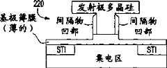
图2A示出了形成在半导体衬底(没有具体给出)中的现有技术的BJT 200。BJT包括限定在浅沟隔离(STI)区之间的集电区202、设置在集电区202顶上的基极薄膜204和形成在基极层204上的发射极结构206。发射极结构206通常由多晶硅形成。间隔物形成在发射极结构两侧的任一侧。器件200是通过本领域技术人员公知的步骤(例如,接触形式等)完成的,因此不需要再详细说明。FIG. 2A shows a
BJT 200的元件的示意性尺寸是:The schematic dimensions of the components of the
基极薄膜的厚度(图中的垂直向)为:10至50nm;The thickness of the base film (vertical direction in the figure) is: 10 to 50nm;
集电区的宽度(图中水平向,STI之间)为:100至200nm;The width of the collector region (horizontal direction in the figure, between STIs) is: 100 to 200nm;
间隔物的宽度/厚度(图中水平向)为:10至50nm;The width/thickness (horizontal direction in the figure) of the spacer is: 10 to 50 nm;
应力层的厚度(图中垂直向)为:10至50nm(如下所述,由于可以仅部分地埋入应力层,所以其能够具有与下面的基极薄膜相同的或甚至更大的厚度);The thickness of the stress layer (vertical direction in the figure) is: 10 to 50 nm (as described below, since the stress layer can be only partially buried, it can have the same or even greater thickness than the underlying base film);
发射极结构的整体高度为:100至200nm;The overall height of the emitter structure is: 100 to 200 nm;
发射极的宽度为:100至200nm。Width of the emitter: 100 to 200 nm.
按照本发明,使用非固有的“应力层”制造双极型晶体管,用于增强固有基极中的电子和空穴的迁移率。应力层(其可以是SiGe)在器件中既产生拉伸应变也产生压缩应变。通常,应力层至少部分地埋在基极层底下,并具有与底下的基极层不同的晶格常数,由此在临近的且在其下面的区域中产生应力。具体的益处是形成在发射极下面的固有基极区中的拉伸和压缩应变,其分别提高了电子和空穴的迁移率。According to the present invention, bipolar transistors are fabricated using an extrinsic "stress layer" for enhancing the mobility of electrons and holes in the intrinsic base. The stressor layer, which may be SiGe, creates both tensile and compressive strains in the device. Typically, the stressor layer is at least partially buried beneath the base layer and has a different lattice constant than the underlying base layer, thereby creating stress in the adjacent and underlying region. A particular benefit is the development of tensile and compressive strains in the intrinsic base region below the emitter, which increase the mobility of electrons and holes, respectively.
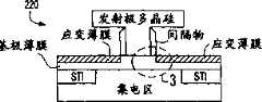
图2B和2C示出了按照本发明的BJT 200的实施例。集电区202限定在两个STI区之间的衬底中,基极薄膜204设置在集电区的顶上,发射极结构206设置在基极薄膜的顶上,间隔物形成在发射极结构的侧面。这些元件的典型尺寸可以与BJT 200中的一样。2B and 2C illustrate an embodiment of a
使用任何适当的刻蚀步骤在发射极结构的两侧(即,临近侧壁间隔物)的基极薄膜中形成凹部。凹部适宜地约为10至25nm深(图中垂直向),横向延伸到集电区之外且在STI之上。由此基极薄膜的“变薄的”层具有大约25至45nm的厚度。Recesses are formed in the base film on both sides of the emitter structure (ie, adjacent to the sidewall spacers) using any suitable etching step. The recess is suitably about 10 to 25nm deep (vertically in the figure), extending laterally beyond the collector region and above the STI. The "thinned" layer of the base film thus has a thickness of approximately 25 to 45 nm.
然后使用已知的工艺由外延生长的应力层填充该凹部。这包括过填充该凹部。由此形成的应力层具有大约10至100nm(基本上等于凹部的深度)的厚度。可以掺杂该应力层以连接发射极结构下的固有基极。The recess is then filled with an epitaxially grown stress layer using known processes. This includes overfilling the recess. The stress layer thus formed has a thickness of approximately 10 to 100 nm (substantially equal to the depth of the recess). This stressor layer can be doped to connect the intrinsic base under the emitter structure.
图2C所示的最终结构包括发射极多晶硅,并可以包括高掺杂的较低电阻的非固有基极。The final structure shown in FIG. 2C includes emitter polysilicon and may include a highly doped lower resistance extrinsic base.
图3示出了图2C的最终结构中的应变。SiGe层(“应力层”)在垂直方向产生拉伸应变,该方向平行于由图2D中垂直双箭头显示的电子流的方向(电子流由图1中的单箭头表示)。拉伸应变将增强电子迁移率并减少穿越时间,增加电流和跨导。应力层也产生垂直于电子流方向的压缩应变,电子流方向由图3中水平单箭头表示(如果在图3中显示的话,在发射极的左侧将具有另一个向内的点箭头)。压缩应变增强固有基极区中的空穴迁移率。Figure 3 shows the strain in the final structure of Figure 2C. The SiGe layer ("stress layer") is tensile strained in a vertical direction parallel to the direction of electron flow shown by the vertical double arrows in Figure 2D (electron flow is represented by the single arrow in Figure 1). Tensile strain will enhance electron mobility and reduce transit time, increasing current and transconductance. The stressor layer also produces a compressive strain perpendicular to the direction of electron flow, which is indicated by the single horizontal arrow in Figure 3 (if shown in Figure 3, there would be another dotted arrow pointing inward to the left of the emitter). Compressive strain enhances hole mobility in the intrinsic base region.
示意性实施例illustrative embodiment
图4A至4J示出了用于形成按照本发明BJT 400的示意性实施例的步骤的顺序。图5A示出了按照图4A至4J所示步骤形成的完成的BJT。图5B示出了按照图4A至4J所示步骤形成的完成的BJT的可选实施例。4A to 4J show a sequence of steps for forming an exemplary embodiment of a
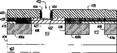
如图4A所示,多个间隔分开的浅沟槽406a、406b、406c(统称406)形成在硅半导体材料的轻掺杂(n)的外延层404,该外延层404已经淀积在重掺杂(n+)单晶硅半导体的副集电极或衬底402上。浅沟槽隔离406填充有隔离氧化物408。使用已知的共形氧化物淀积和氧化物剖光步骤或其它的方法适当地形成浅沟槽隔离(STI)氧化物408,以使氧化物408的表面与外延层404的表面处于同一水平。在沟槽406b与406c之间的层404的最右边直立部分或平台410将最终形成贯穿衬底402的副集电极延伸区,其将是最终BJT的副集电极。As shown in FIG. 4A, a plurality of spaced apart
在沟槽406a与406b之间的层404的最左边直立部分或平台412将最终形成最终的BJT的集电极。The leftmost upright portion or
可优选地形成深沟槽隔离(没有显示)。可优选地形成CMOS层(没有显示)(例如,见美国专利No.6,448,124)。Deep trench isolation (not shown) may preferably be formed. A CMOS layer (not shown) may preferably be formed (eg, see US Patent No. 6,448,124).
在平台410和412的表面上以及隔离氧化物408上淀积刻蚀阻挡阻材料(优选地为二氧化硅)层416和多晶硅薄层(没有显示)。这组层为平台410提供了保护以避免稍后的处理。通过光刻技术限定对应于区域412且与STI 406交迭的区域,刻蚀薄多晶硅层,停止在薄刻蚀阻挡层416。然后优选地使用例如稀释的HF的湿法刻蚀工艺刻蚀层416,暴露出平台412的表面以及部分的相邻氧化物408。A
接下来,如图4B所示,使用非选择性外延淀积技术在平台412的表面以及相邻氧化物408的暴露部分上淀积硅半导体材料层420。层420作为多晶材料淀积在氧化物408上,作为单晶材料(标记为421)淀积在平台412的表面上,并作为多晶硅淀积在416上残留的薄多晶硅层上。掺杂层420,使其在npn型双极器件中具有p型导电类型,在pnp型双极器件中具有n型导电类型。层420的部分421将形成BJT的基极。层420也可以包括硅锗(SiGe)合金,以便形成异质结的双极型晶体管(HBT)。层420/421在平台412(开口中)上以及层416和418上具有大约10至50nm的厚度。Next, as shown in FIG. 4B , a silicon
可以使用任何已知的外延淀积技术来淀积层420(421),该淀积技术在临近平台412的氧化物区域408上以及平台410上分别提供预期的多晶和单晶区域。优选的方法是使用低温外延(LTE)技术淀积层420/421。硼或磷可分别用作p型或n型导电类型的掺杂剂,并可以具有5×1018至5×1019cm-3的掺杂浓度。以此方式,在公知方式的淀积步骤期间,通过简单的引入适当的组分形成了硼或磷掺杂的硅或硅/锗的淀积层420/421。Layer 420 (421) may be deposited using any known epitaxial deposition technique that provides the desired polycrystalline and monocrystalline regions on
在淀积层420/421之后,淀积氧化物层422和氮化物层424。可以半导体制造领域技术人员熟知的方式淀积这些层。可选择地使用公知的现有技术来热生长氧化物层422。氧化物层422具有大约10至20nm的典型厚度。氮化物层424具有大约100至200nm的典型厚度。After depositing
接下来,如图4C所示,使用光刻和刻蚀来图形化氮化物424,并停止在氧化物422上。然后去除氧化物422,留下发射极轴心结构426。发射极轴心426具有大约100至200nm的典型高度,大约100至200nm的典型宽度,并且大约位于平台412顶上的固有基极421的中心。发射极轴心426包括刻蚀的氮化物424(在此附图中显示为424′)和刻蚀的氧化物422(在此附图中显示为422′)。Next, as shown in FIG. 4C , photolithography and etching are used to pattern the nitride 424 , stopping on the
接下来,如图4D所示,使用发射极轴心426作为掩膜通过RIE(反应离子刻蚀)或湿法刻蚀来刻蚀固有基极421。由此产生薄的固有基极421(在此附图中显示为421′)。其也产生变薄的硅层420(在此附图中显示为420′)。薄的SiGe层421′成为固有基极。Next, as shown in FIG. 4D , the
接下来,如图4E所示,外延生长应力层450。应力层显示为覆盖硅420的450以及覆盖SiGe 421′的451。应力层生长到至少达到氧化物422的高度,包括超过薄层421′的原始高度,在任一种情况中均被埋入。凹部尺寸大约为5至25nm。应力层厚度大约为5至50nm。对于npn型双极型器件,应力层的晶格常数大于固有基极的晶格常数。在此情况下,对于硅基极421′,应力层是硅锗(SiGe),而对于SiGe层421′,应力层是具有更高锗含量的SiGe。另一方面,对于pnp型双极型器件,应力层的晶格常数小于固有基极421′的晶格常数。在此情况下,对于硅基极421′,应力层是碳化硅(SiC),而对于SiGe层421′,应力层是具有更低锗含量的SiGe、或者硅、或者碳化硅。Next, as shown in FIG. 4E , the
接下来,如图4F所示,淀积并平坦化氧化物428。氧化物428具有与发射极轴心426的氮化物424相同的厚度(图中垂直向)。Next, an
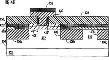
接下来,如图4G所示,使用底层氧化物422′作为刻蚀阻挡,通过选择性刻蚀去除发射极轴心426的氮化物424,在氧化物428中产生“发射极”开口432。此步骤中,开口432向下延伸到氧化物422′。开口432具有与发射极轴心426的宽度相等的宽度(图中水平向)。氮化物间隔物434形成在开口432的侧壁上。间隔物434具有大约10至50nm的典型厚度(图中水平向)。由此在侧壁间隔物434之间产生具有大约100至200nm的典型宽度的发射极开口。Next, as shown in FIG. 4G , using the
接下来,如图4H所示,刻蚀底层氧化物422′,在发射极开口432中暴露出基极层421′。然后淀积多晶硅。淀积(氮化物)硬掩膜436。使用光刻来图形化氮化物硬掩膜436并进行刻蚀。然后将氮化物硬掩膜436用于刻蚀多晶硅,产生图4H中所示的发射极结构430。T型发射极结构的垂直(直立)部分位于发射极开口432中。T型发射极结构的水平(横向)部分延伸在该氧化物428上。Next, as shown in FIG. 4H , the
接下来,如图4I所示,使用湿法刻蚀或RIE刻蚀工艺刻蚀位于发射极结构突出延伸(水平)部分下面的所有的氧化物428。残留的氧化物在图中显示为428′。如图4I所示,通过氧化物硬掩膜淀积、光刻和停止在氧化物层416上的基极多晶硅的RIE刻蚀,限定了非固有基极区域层420″/450′。稍后去除硬掩膜氧化物和氧化物层416,产生如图4I所示的晶体管结构。Next, as shown in FIG. 41 , all of the
接下来,如图4J所示,在全部的结构436、430、428′上形成氮化物侧壁间隔物438。如图4J所示,通过金属溅射淀积、反应和转变的已知工艺形成硅化物层。硅化物只形成在暴露的硅上。硅化物440a形成在位于发射极430左侧的SiGe/多晶硅450′/420″部分上。硅化物440b形成在位于发射极430右侧的SiGe/多晶硅450′/420″部分上。硅化物440c形成在平台410暴露出的硅上,但不形成在相邻平台410暴露出的氧化物408上。Next, as shown in FIG. 4J ,
在最后一组步骤中,如图5A所示,通过淀积氧化物电介质452并形成分别用于发射极、基极和集电极的接触454a、454b和454c,完成了BJT器件400的处理。In a final set of steps, as shown in FIG. 5A, processing of the
在可选实施例中,如图5B所示,在应力层顶上淀积额外的掺杂多晶硅层560,其成为凸出的非固有基极的一部分。在此情况下,通过增加多晶硅层560中的掺杂水平可进一步降低基极电阻,而不增加寄生的集电极-基极电容。更具体地,应变SiGe层的晶体区域减少了掺杂剂从多晶硅层560向集电极区412的扩散。相比于在Si中而言,降低的掺杂剂扩散在SiGe中产生较低的硼扩散系数。In an alternative embodiment, as shown in Figure 5B, an additional doped polysilicon layer 560 is deposited on top of the stressor layer, which becomes part of the raised extrinsic base. In this case, the base resistance can be further reduced by increasing the doping level in the polysilicon layer 560 without increasing the parasitic collector-base capacitance. More specifically, straining the crystalline region of the SiGe layer reduces the diffusion of dopants from the polysilicon layer 560 to the
仿真结果Simulation results
图6至8示出了结合应力层的仿真效果。Figures 6 to 8 show the simulation effects of incorporating stress layers.
图6示出了感兴趣的半个器件区域的剖面图。两个轴都是以微米显示距离。为了仿真效率,只显示了半个器件。应力层在基极薄膜的顶上。在该结构中显示了表示横向应力的等值应力线。在发射极层的垂直部分底下,横向应力是压缩的,在基极薄膜与发射极薄膜之间的界面附近具有最大的应力。在应力层底下,基极层应力是拉伸的,在表面附近也具有最大幅度。Figure 6 shows a cross-sectional view of the half device area of interest. Both axes display distances in microns. For simulation efficiency, only half of the device is shown. A stressor layer is on top of the base film. Equivalent stress lines representing transverse stresses are shown in this structure. Underneath the vertical portion of the emitter layer, the lateral stress is compressive, with maximum stress near the interface between the base and emitter films. Beneath the stressed layer, the base layer stress is tensile and also has a maximum magnitude near the surface.
图7显示了与图6相同的结构,而等值应力线表示垂直应力。两个轴都是以微米显示距离。在此,发射极薄膜底下的基极薄膜是垂直拉伸的应力,在表面附近具有最大幅度。Figure 7 shows the same structure as in Figure 6, while the isovalue stress lines represent the vertical stress. Both axes display distances in microns. Here, the base film underlying the emitter film is vertically tensile, with the greatest magnitude near the surface.
图8显示了在图6和7中所示的“eSiGe材料”表面下面10nm的“图示”位置处的应力图。水平轴是以微米表示的距离,垂直轴是以Mpa表示的应力(在此,例如0微米处Sxx大约是-375Mpa)。正的拉伸应变值表示拉伸,而负值表示压缩。埋入的SiGe的边缘(在图6和7中标记为eSiGe)位于0.14微米处,由图中垂直的虚线表示。Figure 8 shows the stress map at the "illustrated" position 10 nm below the surface of the "eSiGe material" shown in Figures 6 and 7 . The horizontal axis is the distance in microns, and the vertical axis is the stress in Mpa (here, for example, Sxx at 0 micron is about -375Mpa). Positive tensile strain values indicate tension, while negative values indicate compression. The edge of the buried SiGe (labeled eSiGe in Figures 6 and 7) is located at 0.14 microns, indicated by the vertical dashed line in the figure.
图6和7的两组分别表示横向应力(SXX)和垂直应力(SYY),能够看出在该器件的固有部分中具有垂直拉伸应力和横向压缩应力。The two groups of Figures 6 and 7 represent lateral stress (SXX) and vertical stress (SYY), respectively, and it can be seen that there is vertical tensile stress and lateral compressive stress in the intrinsic part of the device.
这表示应力层具有在该器件的固有部分中产生垂直拉伸应力和横向压缩应力的特性。This indicates that the stressor layer has the property of generating vertical tensile stress and lateral compressive stress in the intrinsic part of the device.
已经主要关于n型(npn:npn)BJT说明了本发明。从上面阐述的教授内容可知,与本发明最有关联的本领域普通技术人员应当意识到,对于p型(pnp)BJT来讲,空穴和电子可以被颠倒(相互替换),拉伸应力和压缩应力可以被颠倒,并且可以使用具有比固有基极晶格常数更低的晶格常数而不是更高的晶格常数的应力层。此外,如上所述,同样适用于较高(对于npn)和较低(对于pnp)的Ge含量。因此,因为与本发明相关,这些内容应当被视为等价物(处于解释权利要求覆盖范围的目的)。The invention has been described mainly in relation to n-type (npn:npn) BJTs. From the teachings set forth above, those of ordinary skill in the art most relevant to the present invention will appreciate that for a p-type (pnp) BJT, holes and electrons can be reversed (replaced for each other), tensile stress and The compressive stress can be reversed and a stressed layer with a lower rather than a higher lattice constant than the intrinsic base lattice constant can be used. Furthermore, as mentioned above, the same applies to higher (for npn) and lower (for pnp) Ge contents. Accordingly, these should be considered equivalents (for purposes of explaining the scope of claim coverage) as they relate to the present invention.
尽管已经关于某种优选实施例或多种优选实施例显示并说明了本发明,但是对于本领域技术人员来说,在阅读并理解了本说明以及附图之后,可以实施某种等价的替换和修改。特别地,关于由上述部件(组件、器件、电路等)执行的各种功能,用于说明这些部件的术语(包括提及的“装置”)倾向于对应(除非以其它方式指出)任何执行所述部件的具体功能的部件(即,功能上等价),即使结构上没有等价于执行此处本发明典型实施例所示功能的结构。此外,尽管已经关于几个实施例中的一个说明了本发明的具体特征,但是对于任何给定的或特别的应用,这样的特征可与其它实施例的一个或多个特征组合获得预期的优点。Although the present invention has been shown and described with respect to a certain preferred embodiment or embodiments, certain equivalent substitutions will be possible to those skilled in the art after a reading and understanding of this specification and the accompanying drawings. and modify. In particular, with respect to the various functions performed by the components (components, devices, circuits, etc.) described above, terms used to describe these components (including references to "means") are intended to correspond (unless otherwise indicated) to any components that perform the specified functions of those described (ie, functional equivalents), even if there is no structural equivalent to structures performing the functions illustrated in the exemplary embodiments of the invention herein. Furthermore, although specific features of the invention have been described with respect to one of several embodiments, for any given or particular application, such features may be combined with one or more features of other embodiments to achieve the desired advantages .
Claims (20)
Applications Claiming Priority (2)
| Application Number | Priority Date | Filing Date | Title |
|---|---|---|---|
| US10/931,660US7102205B2 (en) | 2004-09-01 | 2004-09-01 | Bipolar transistor with extrinsic stress layer |
| US10/931,660 | 2004-09-01 |
Publications (2)
| Publication Number | Publication Date |
|---|---|
| CN1763968Atrue CN1763968A (en) | 2006-04-26 |
| CN100407442C CN100407442C (en) | 2008-07-30 |
Family
ID=35941887
Family Applications (1)
| Application Number | Title | Priority Date | Filing Date |
|---|---|---|---|
| CN2005100978284AExpired - Fee RelatedCN100407442C (en) | 2004-09-01 | 2005-08-30 | bipolar device |
Country Status (4)
| Country | Link |
|---|---|
| US (1) | US7102205B2 (en) |
| JP (1) | JP5107512B2 (en) |
| CN (1) | CN100407442C (en) |
| TW (1) | TW200623392A (en) |
Cited By (6)
| Publication number | Priority date | Publication date | Assignee | Title |
|---|---|---|---|---|
| CN103000674A (en)* | 2012-12-14 | 2013-03-27 | 复旦大学 | Transistor and manufacturing method thereof |
| CN102082172B (en)* | 2009-11-26 | 2013-04-24 | 上海华虹Nec电子有限公司 | Polycrystalline triode manufactured by applying germanium silicon technology and manufacture method thereof |
| WO2014089813A1 (en)* | 2012-12-14 | 2014-06-19 | 复旦大学 | Transistor and manufacturing method thereof |
| CN104425577A (en)* | 2013-08-30 | 2015-03-18 | 上海华虹宏力半导体制造有限公司 | Self-alignment germanium-silicon heterojunction bipolar triode device and manufacturing method thereof |
| CN104900686A (en)* | 2014-03-03 | 2015-09-09 | 中芯国际集成电路制造(上海)有限公司 | Transistor and manufacturing method thereof |
| CN108400162A (en)* | 2017-02-08 | 2018-08-14 | 格芯公司 | The heterojunction bipolar transistor with stress material for improving mobility |
Families Citing this family (31)
| Publication number | Priority date | Publication date | Assignee | Title |
|---|---|---|---|---|
| US7329941B2 (en)* | 2004-07-20 | 2008-02-12 | International Business Machines Corporation | Creating increased mobility in a bipolar device |
| US7262484B2 (en)* | 2005-05-09 | 2007-08-28 | International Business Machines Corporation | Structure and method for performance improvement in vertical bipolar transistors |
| US8407634B1 (en) | 2005-12-01 | 2013-03-26 | Synopsys Inc. | Analysis of stress impact on transistor performance |
| US7342293B2 (en)* | 2005-12-05 | 2008-03-11 | International Business Machines Corporation | Bipolar junction transistors (BJTS) with second shallow trench isolation (STI) regions, and methods for forming same |
| JP2007250903A (en)* | 2006-03-16 | 2007-09-27 | Matsushita Electric Ind Co Ltd | Heterojunction bipolar transistor and manufacturing method thereof |
| WO2007122698A1 (en)* | 2006-04-18 | 2007-11-01 | Panasonic Corporation | Ultrasonograph |
| US7888745B2 (en)* | 2006-06-21 | 2011-02-15 | International Business Machines Corporation | Bipolar transistor with dual shallow trench isolation and low base resistance |
| US7772676B2 (en)* | 2006-06-23 | 2010-08-10 | Infineon Technologies Ag | Strained semiconductor device and method of making same |
| JP2008041899A (en)* | 2006-08-04 | 2008-02-21 | Toshiba Corp | Semiconductor device |
| KR100817403B1 (en)* | 2006-11-20 | 2008-03-27 | 전북대학교산학협력단 | Semiconductor device structure and manufacturing method thereof |
| US7557010B2 (en)* | 2007-02-12 | 2009-07-07 | Agere Systems Inc. | Method to improve writer leakage in a SiGe bipolar device |
| CN101641792B (en) | 2007-02-22 | 2012-03-21 | 富士通半导体股份有限公司 | Semiconductor device and process for producing the same |
| US7982269B2 (en)* | 2008-04-17 | 2011-07-19 | International Business Machines Corporation | Transistors having asymmetric strained source/drain portions |
| US7964465B2 (en)* | 2008-04-17 | 2011-06-21 | International Business Machines Corporation | Transistors having asymmetric strained source/drain portions |
| EP2315238B1 (en)* | 2009-10-26 | 2012-06-20 | Nxp B.V. | Heterojunction Bipolar Transistor |
| CN101866947A (en)* | 2010-05-12 | 2010-10-20 | 上海宏力半导体制造有限公司 | Silicon germanium heterojunction bipolar transistor |
| US20120313146A1 (en) | 2011-06-08 | 2012-12-13 | International Business Machines Corporation | Transistor and method of forming the transistor so as to have reduced base resistance |
| US8603883B2 (en)* | 2011-11-16 | 2013-12-10 | International Business Machines Corporation | Interface control in a bipolar junction transistor |
| US9817928B2 (en) | 2012-08-31 | 2017-11-14 | Synopsys, Inc. | Latch-up suppression and substrate noise coupling reduction through a substrate back-tie for 3D integrated circuits |
| US9190346B2 (en) | 2012-08-31 | 2015-11-17 | Synopsys, Inc. | Latch-up suppression and substrate noise coupling reduction through a substrate back-tie for 3D integrated circuits |
| US8847324B2 (en) | 2012-12-17 | 2014-09-30 | Synopsys, Inc. | Increasing ION /IOFF ratio in FinFETs and nano-wires |
| US9379018B2 (en) | 2012-12-17 | 2016-06-28 | Synopsys, Inc. | Increasing Ion/Ioff ratio in FinFETs and nano-wires |
| US8975146B2 (en)* | 2013-05-01 | 2015-03-10 | International Business Machines Corporation | Trench isolation structures and methods for bipolar junction transistors |
| US9608096B1 (en) | 2015-10-02 | 2017-03-28 | Globalfoundries Inc. | Implementing stress in a bipolar junction transistor |
| US9825157B1 (en) | 2016-06-29 | 2017-11-21 | Globalfoundries Inc. | Heterojunction bipolar transistor with stress component |
| US10847409B2 (en)* | 2018-09-27 | 2020-11-24 | Taiwan Semiconductor Manufacturing Company, Ltd. | Semiconductor device and method |
| US11145725B2 (en)* | 2019-09-23 | 2021-10-12 | Globalfoundries U.S. Inc. | Heterojunction bipolar transistor |
| US11721722B2 (en) | 2021-08-27 | 2023-08-08 | Globalfoundries U.S. Inc. | Bipolar junction transistors including a stress liner |
| US20230178638A1 (en)* | 2021-12-06 | 2023-06-08 | Globalfoundries Singapore Pte. Ltd. | Bipolar transistors |
| US12336206B2 (en) | 2022-11-21 | 2025-06-17 | Globalfoundries U.S. Inc. | Heterojunction bipolar transistors with a cut stress liner |
| US12211929B1 (en)* | 2024-05-14 | 2025-01-28 | Globalfoundries U.S. Inc. | Heterojunction bipolar transistors with terminals having a non-planar arrangement |
Family Cites Families (14)
| Publication number | Priority date | Publication date | Assignee | Title |
|---|---|---|---|---|
| JPH0766981B2 (en)* | 1987-03-26 | 1995-07-19 | 日本電気株式会社 | Infrared sensor |
| JPH04179235A (en)* | 1990-11-14 | 1992-06-25 | Toshiba Corp | heterojunction bipolar transistor |
| JP3085553B2 (en)* | 1991-11-20 | 2000-09-11 | 日本電信電話株式会社 | Surface structure of semiconductor device |
| JPH06275814A (en)* | 1993-03-17 | 1994-09-30 | Sankyo Seiki Mfg Co Ltd | Semiconductor material |
| JP3326427B2 (en)* | 1996-09-17 | 2002-09-24 | 松下電器産業株式会社 | Semiconductor device and manufacturing method thereof |
| FR2804247B1 (en)* | 2000-01-21 | 2002-04-12 | St Microelectronics Sa | METHOD FOR PRODUCING A BIPOLAR TRANSISTOR WITH SELF-ALIGNED EXTRINSIC BASE |
| US20030199153A1 (en)* | 2000-01-27 | 2003-10-23 | Kovacic Stephen J. | Method of producing SI-GE base semiconductor devices |
| WO2002061842A1 (en)* | 2001-01-31 | 2002-08-08 | Matsushita Electric Industrial Co., Ltd. | Semiconductor crystal film and method for preparation thereof |
| JP4569026B2 (en)* | 2001-03-30 | 2010-10-27 | 信越半導体株式会社 | Semiconductor substrate and manufacturing method thereof |
| WO2002099890A1 (en)* | 2001-06-05 | 2002-12-12 | Sony Corporation | Semiconductor layer and forming method therefor, and semiconductor device and production method therefor |
| JP2003151987A (en)* | 2001-11-19 | 2003-05-23 | Mitsubishi Heavy Ind Ltd | Semiconductor substrate and method of manufacturing semiconductor substrate |
| JP4182177B2 (en)* | 2002-10-30 | 2008-11-19 | 富士通マイクロエレクトロニクス株式会社 | Manufacturing method of semiconductor device |
| US7101742B2 (en)* | 2003-08-12 | 2006-09-05 | Taiwan Semiconductor Manufacturing Company, Ltd. | Strained channel complementary field-effect transistors and methods of manufacture |
| US7005359B2 (en)* | 2003-11-17 | 2006-02-28 | Intel Corporation | Bipolar junction transistor with improved extrinsic base region and method of fabrication |
- 2004
- 2004-09-01USUS10/931,660patent/US7102205B2/ennot_activeExpired - Lifetime
- 2005
- 2005-08-29JPJP2005247839Apatent/JP5107512B2/ennot_activeExpired - Fee Related
- 2005-08-30CNCN2005100978284Apatent/CN100407442C/ennot_activeExpired - Fee Related
- 2005-08-31TWTW094129854Apatent/TW200623392A/enunknown
Cited By (10)
| Publication number | Priority date | Publication date | Assignee | Title |
|---|---|---|---|---|
| CN102082172B (en)* | 2009-11-26 | 2013-04-24 | 上海华虹Nec电子有限公司 | Polycrystalline triode manufactured by applying germanium silicon technology and manufacture method thereof |
| CN103000674A (en)* | 2012-12-14 | 2013-03-27 | 复旦大学 | Transistor and manufacturing method thereof |
| WO2014089813A1 (en)* | 2012-12-14 | 2014-06-19 | 复旦大学 | Transistor and manufacturing method thereof |
| CN104425577A (en)* | 2013-08-30 | 2015-03-18 | 上海华虹宏力半导体制造有限公司 | Self-alignment germanium-silicon heterojunction bipolar triode device and manufacturing method thereof |
| CN104425577B (en)* | 2013-08-30 | 2017-08-08 | 上海华虹宏力半导体制造有限公司 | Autoregistration germanium-silicon heterojunction bipolar triode device and its manufacture method |
| CN104900686A (en)* | 2014-03-03 | 2015-09-09 | 中芯国际集成电路制造(上海)有限公司 | Transistor and manufacturing method thereof |
| CN104900686B (en)* | 2014-03-03 | 2018-10-26 | 中芯国际集成电路制造(上海)有限公司 | Transistor and its manufacturing method |
| CN108400162A (en)* | 2017-02-08 | 2018-08-14 | 格芯公司 | The heterojunction bipolar transistor with stress material for improving mobility |
| CN108400162B (en)* | 2017-02-08 | 2021-03-30 | 格芯(美国)集成电路科技有限公司 | Heterojunction bipolar transistors with stressed materials for improved mobility |
| US11876123B2 (en) | 2017-02-08 | 2024-01-16 | Globalfoundries U.S. Inc. | Heterojunction bipolar transistors with stress material for improved mobility |
Also Published As
| Publication number | Publication date |
|---|---|
| US20060043529A1 (en) | 2006-03-02 |
| US7102205B2 (en) | 2006-09-05 |
| CN100407442C (en) | 2008-07-30 |
| JP2006074040A (en) | 2006-03-16 |
| TW200623392A (en) | 2006-07-01 |
| JP5107512B2 (en) | 2012-12-26 |
Similar Documents
| Publication | Publication Date | Title |
|---|---|---|
| CN100407442C (en) | bipolar device | |
| US7741186B2 (en) | Creating increased mobility in a bipolar device | |
| CN1225797C (en) | Semiconductor device and manufacturing method thereof | |
| CN100345308C (en) | Semiconductor element and its manufacturing method | |
| CN1661811A (en) | Ultrathin SOI Vertical Bipolar Transistor and Method | |
| CN107546264B (en) | Heterojunction bipolar transistor with stress component | |
| CN101908543B (en) | Integrated circuit structure | |
| CN103022107B (en) | Fin bipolar junction transistor and manufacture method | |
| CN107342319B (en) | A compound strained Si/SiGe heterojunction bipolar transistor and its preparation method | |
| CN1398432A (en) | Bipolar transistor and method of manufacturing the same | |
| CN103956323A (en) | Semiconductor and manufacturing method thereof, and non-instantaneous computer readable storage medium | |
| CN1825625A (en) | Strained transistor with hybrid strain-inducing layer and method of forming same | |
| CN1303696C (en) | Process for making high voltage NPN bipolar device with improved AC performance | |
| CN1717793A (en) | Method for producing bipolar transistors | |
| CN1790638A (en) | Metal Oxide Semiconductor Field Effect Transistor with Localized Stress Structure | |
| CN1941296A (en) | In-situ silicon-germanium doped and silicon carbide source leakage pole area for strain silicon CMOS transistor | |
| CN1841684A (en) | Manufacturing method of semiconductor device | |
| US9263345B2 (en) | SOI transistors with improved source/drain structures with enhanced strain | |
| CN101060121A (en) | Semiconductor structure and fabrication method thereof | |
| CN1645616A (en) | Semiconductor chip and semiconductor component and method for forming the same | |
| SE522891C2 (en) | A silicon-germanium mesa transistor, a method for its preparation and an integrated circuit comprising such a transistor | |
| US7846806B1 (en) | System and method for providing a self aligned silicon germanium (SiGe) heterojunction bipolar transistor using a mesa emitter-base architecture | |
| JP5090163B2 (en) | Bipolar transistor and manufacturing method thereof | |
| US11804542B2 (en) | Annular bipolar transistors | |
| US12040388B2 (en) | Lateral bipolar transistors |
Legal Events
| Date | Code | Title | Description |
|---|---|---|---|
| C06 | Publication | ||
| PB01 | Publication | ||
| C10 | Entry into substantive examination | ||
| SE01 | Entry into force of request for substantive examination | ||
| C14 | Grant of patent or utility model | ||
| GR01 | Patent grant | ||
| TR01 | Transfer of patent right | Effective date of registration:20171122 Address after:Grand Cayman, Cayman Islands Patentee after:GLOBALFOUNDRIES INC. Address before:American New York Patentee before:Core USA second LLC Effective date of registration:20171122 Address after:American New York Patentee after:Core USA second LLC Address before:American New York Patentee before:International Business Machines Corp. | |
| TR01 | Transfer of patent right | ||
| CF01 | Termination of patent right due to non-payment of annual fee | Granted publication date:20080730 | |
| CF01 | Termination of patent right due to non-payment of annual fee |