CN1756654A - Sheeting and wiring plate - Google Patents
Sheeting and wiring plateDownload PDFInfo
- Publication number
- CN1756654A CN1756654ACNA200380109996XACN200380109996ACN1756654ACN 1756654 ACN1756654 ACN 1756654ACN A200380109996X ACNA200380109996X ACN A200380109996XACN 200380109996 ACN200380109996 ACN 200380109996ACN 1756654 ACN1756654 ACN 1756654A
- Authority
- CN
- China
- Prior art keywords
- layer
- sheet material
- wiring board
- wiring
- temperature
- Prior art date
- Legal status (The legal status is an assumption and is not a legal conclusion. Google has not performed a legal analysis and makes no representation as to the accuracy of the status listed.)
- Granted
Links
Images


Classifications
- H—ELECTRICITY
- H05—ELECTRIC TECHNIQUES NOT OTHERWISE PROVIDED FOR
- H05K—PRINTED CIRCUITS; CASINGS OR CONSTRUCTIONAL DETAILS OF ELECTRIC APPARATUS; MANUFACTURE OF ASSEMBLAGES OF ELECTRICAL COMPONENTS
- H05K3/00—Apparatus or processes for manufacturing printed circuits
- H05K3/46—Manufacturing multilayer circuits
- H05K3/4644—Manufacturing multilayer circuits by building the multilayer layer by layer, i.e. build-up multilayer circuits
- H05K3/4673—Application methods or materials of intermediate insulating layers not specially adapted to any one of the previous methods of adding a circuit layer
- B—PERFORMING OPERATIONS; TRANSPORTING
- B32—LAYERED PRODUCTS
- B32B—LAYERED PRODUCTS, i.e. PRODUCTS BUILT-UP OF STRATA OF FLAT OR NON-FLAT, e.g. CELLULAR OR HONEYCOMB, FORM
- B32B7/00—Layered products characterised by the relation between layers; Layered products characterised by the relative orientation of features between layers, or by the relative values of a measurable parameter between layers, i.e. products comprising layers having different physical, chemical or physicochemical properties; Layered products characterised by the interconnection of layers
- B32B7/04—Interconnection of layers
- B32B7/12—Interconnection of layers using interposed adhesives or interposed materials with bonding properties
- H—ELECTRICITY
- H05—ELECTRIC TECHNIQUES NOT OTHERWISE PROVIDED FOR
- H05K—PRINTED CIRCUITS; CASINGS OR CONSTRUCTIONAL DETAILS OF ELECTRIC APPARATUS; MANUFACTURE OF ASSEMBLAGES OF ELECTRICAL COMPONENTS
- H05K2201/00—Indexing scheme relating to printed circuits covered by H05K1/00
- H05K2201/01—Dielectrics
- H05K2201/0137—Materials
- H05K2201/0154—Polyimide
- H—ELECTRICITY
- H05—ELECTRIC TECHNIQUES NOT OTHERWISE PROVIDED FOR
- H05K—PRINTED CIRCUITS; CASINGS OR CONSTRUCTIONAL DETAILS OF ELECTRIC APPARATUS; MANUFACTURE OF ASSEMBLAGES OF ELECTRICAL COMPONENTS
- H05K2201/00—Indexing scheme relating to printed circuits covered by H05K1/00
- H05K2201/01—Dielectrics
- H05K2201/0183—Dielectric layers
- H05K2201/0195—Dielectric or adhesive layers comprising a plurality of layers, e.g. in a multilayer structure
- H—ELECTRICITY
- H05—ELECTRIC TECHNIQUES NOT OTHERWISE PROVIDED FOR
- H05K—PRINTED CIRCUITS; CASINGS OR CONSTRUCTIONAL DETAILS OF ELECTRIC APPARATUS; MANUFACTURE OF ASSEMBLAGES OF ELECTRICAL COMPONENTS
- H05K2201/00—Indexing scheme relating to printed circuits covered by H05K1/00
- H05K2201/03—Conductive materials
- H05K2201/0332—Structure of the conductor
- H05K2201/0335—Layered conductors or foils
- H05K2201/0358—Resin coated copper [RCC]
- H—ELECTRICITY
- H05—ELECTRIC TECHNIQUES NOT OTHERWISE PROVIDED FOR
- H05K—PRINTED CIRCUITS; CASINGS OR CONSTRUCTIONAL DETAILS OF ELECTRIC APPARATUS; MANUFACTURE OF ASSEMBLAGES OF ELECTRICAL COMPONENTS
- H05K3/00—Apparatus or processes for manufacturing printed circuits
- H05K3/46—Manufacturing multilayer circuits
- H05K3/4644—Manufacturing multilayer circuits by building the multilayer layer by layer, i.e. build-up multilayer circuits
- Y—GENERAL TAGGING OF NEW TECHNOLOGICAL DEVELOPMENTS; GENERAL TAGGING OF CROSS-SECTIONAL TECHNOLOGIES SPANNING OVER SEVERAL SECTIONS OF THE IPC; TECHNICAL SUBJECTS COVERED BY FORMER USPC CROSS-REFERENCE ART COLLECTIONS [XRACs] AND DIGESTS
- Y10—TECHNICAL SUBJECTS COVERED BY FORMER USPC
- Y10T—TECHNICAL SUBJECTS COVERED BY FORMER US CLASSIFICATION
- Y10T428/00—Stock material or miscellaneous articles
- Y10T428/24—Structurally defined web or sheet [e.g., overall dimension, etc.]
- Y10T428/24802—Discontinuous or differential coating, impregnation or bond [e.g., artwork, printing, retouched photograph, etc.]
- Y10T428/24917—Discontinuous or differential coating, impregnation or bond [e.g., artwork, printing, retouched photograph, etc.] including metal layer
- Y—GENERAL TAGGING OF NEW TECHNOLOGICAL DEVELOPMENTS; GENERAL TAGGING OF CROSS-SECTIONAL TECHNOLOGIES SPANNING OVER SEVERAL SECTIONS OF THE IPC; TECHNICAL SUBJECTS COVERED BY FORMER USPC CROSS-REFERENCE ART COLLECTIONS [XRACs] AND DIGESTS
- Y10—TECHNICAL SUBJECTS COVERED BY FORMER USPC
- Y10T—TECHNICAL SUBJECTS COVERED BY FORMER US CLASSIFICATION
- Y10T428/00—Stock material or miscellaneous articles
- Y10T428/249921—Web or sheet containing structurally defined element or component
- Y10T428/249953—Composite having voids in a component [e.g., porous, cellular, etc.]
- Y10T428/249955—Void-containing component partially impregnated with adjacent component
- Y10T428/249958—Void-containing component is synthetic resin or natural rubbers
- Y—GENERAL TAGGING OF NEW TECHNOLOGICAL DEVELOPMENTS; GENERAL TAGGING OF CROSS-SECTIONAL TECHNOLOGIES SPANNING OVER SEVERAL SECTIONS OF THE IPC; TECHNICAL SUBJECTS COVERED BY FORMER USPC CROSS-REFERENCE ART COLLECTIONS [XRACs] AND DIGESTS
- Y10—TECHNICAL SUBJECTS COVERED BY FORMER USPC
- Y10T—TECHNICAL SUBJECTS COVERED BY FORMER US CLASSIFICATION
- Y10T428/00—Stock material or miscellaneous articles
- Y10T428/31504—Composite [nonstructural laminate]
- Y10T428/31678—Of metal
- Y10T428/31681—Next to polyester, polyamide or polyimide [e.g., alkyd, glue, or nylon, etc.]
Landscapes
- Engineering & Computer Science (AREA)
- Manufacturing & Machinery (AREA)
- Microelectronics & Electronic Packaging (AREA)
- Laminated Bodies (AREA)
- Production Of Multi-Layered Print Wiring Board (AREA)
- Insulated Metal Substrates For Printed Circuits (AREA)
Abstract
Description
Translated fromChinese技术领域technical field
本发明涉及使用将2种特性互异的层层叠而成的薄片材料及使用该薄片材料的布线板,特别涉及能够在组合布线板(build up布线板)等半导体封装的布线板中使用、耐裂性高、可靠性优异的薄片材料及布线板。The present invention relates to a sheet material formed by laminating two layers with different properties and a wiring board using the sheet material, and particularly to a wiring board that can be used in semiconductor packages such as build-up wiring boards (build up wiring boards), and is crack-resistant Sheet materials and wiring boards with high reliability and high reliability.
背景技术Background technique
伴随着近来的便携式机器的小型化、多功能化及互联网通信系统的高度化,用于这些用途的半导体元件的端子数量日益增加,端子间距越来越窄。因此,在半导体封装中,对搭载半导体元件的布线板,也提出了前所未有的高密度化及细微布线化的要求。With recent miniaturization and multifunctionalization of portable devices and sophistication of Internet communication systems, the number of terminals of semiconductor elements used for these purposes is increasing, and the pitch between terminals is becoming narrower. Therefore, even in semiconductor packages, higher densification and finer wiring are required than ever before on wiring boards on which semiconductor elements are mounted.
作为具有这种高密度的细微布线的布线板,有在核心(base core)基板的外层设置高密度地形成布线的组合布线层的组合印刷布线板。As a wiring board having such high-density fine wiring, there is a built-up printed wiring board in which a built-up wiring layer in which wiring is formed at a high density is provided on an outer layer of a base core substrate.
图6是表示现有技术的组合印刷布线板的剖面图。如图6所示,在该现有技术的组合印刷布线板中,设置着由环氧玻璃构成的核心基板73,在该核心基板73上,利用钻头形成通路孔71。通路孔71的直径例如约300μm。然后,在核心基板73的两面,形成导体布线72,再设置覆盖该导体布线72的层间绝缘膜75。在层间绝缘膜75上,形成与导体布线72连接的通路孔74,在层间绝缘膜75的表面,设置通过通路孔74与导体布线72连接的导体布线76。此外,根据需要,还往往在导体布线76上反复设置形成通路孔的层间绝缘膜及导体布线,从而将布线板多层布线化。Fig. 6 is a sectional view showing a conventional built-up printed wiring board. As shown in FIG. 6 , in this conventional build-up printed wiring board, a
另外,作为使动作速度进一步提高的布线板,有人提出了没有板芯基板的薄型而且高密度的布线板的方案。它是在金属板等支持体上形成由布线及布线膜构成的布线层,然后除去支持体,从而将所述布线层本身作为布线板(例如,参照特开2001-177010号公报、特开2002-83893号公报及特开2002-198462号公报)。该布线板,是除去通常的组合印刷布线板中的板芯基板后,只使组合层独立的基板,堪称是极限的薄型布线板。In addition, a thin and high-density wiring board without a core substrate has been proposed as a wiring board that further improves the operating speed. In this method, a wiring layer composed of wiring and a wiring film is formed on a support such as a metal plate, and then the support is removed to use the wiring layer itself as a wiring board (for example, refer to JP-A-2001-177010, JP-A-2002 -83893 bulletin and JP-A-2002-198462 bulletin). This wiring board is a substrate in which only the build-up layer is independent after removing the core substrate in a common build-up printed wiring board, and it can be called the ultimate thin wiring board.
在这种布线板中,由于根本没有贯通通路孔,所以不需要设置旨在将布线与贯通通路孔连接的岛(land)部。因此,阻抗的控制容易,环路电感小,布线板整体的动作速度快。所以,使用该布线板后,能够进行高速布线设计。另外,作为支持体,由于使用平坦性优异、弹性率大、耐热性高的金属板,所以可以采用高温工艺,形成形状稳定性高、高密度而且细微的布线图案。In such a wiring board, since there are no through via holes at all, there is no need to provide a land portion for connecting wiring to the through via holes. Therefore, the impedance control is easy, the loop inductance is small, and the operation speed of the wiring board as a whole is fast. Therefore, using this wiring board enables high-speed wiring design. In addition, since a metal plate with excellent flatness, high elastic modulus, and high heat resistance is used as the support, high-temperature processes can be used to form fine wiring patterns with high shape stability and high density.
布线板主要由旨在电连接的金属布线和在该金属布线之间起绝缘作用的绝缘膜构成。作为组合基板等具有高密度的细微布线的布线板的绝缘膜使用的绝缘材料,在现有技术中,使用下列材料。A wiring board is mainly composed of metal wirings intended to be electrically connected and an insulating film that functions as insulation between the metal wirings. As an insulating material used for an insulating film of a wiring board having high-density fine wiring such as a build-up substrate, the following materials are conventionally used.
在采用半添加法或添加法制作的布线板、即采用无电解电镀法及/或电解电镀法形成金属布线的布线板的绝缘膜中,使用由环氧树脂等热硬化性树脂构成的绝缘材料。该绝缘材料以半硬化状态,在基板上层叠,层叠后加热硬化,成为绝缘膜。然后,使用钻头或激光,制作通路孔后,实施去污(デスミア)等处理,采用无电解电镀法及/或电解电镀法形成金属布线。An insulating material made of a thermosetting resin such as epoxy resin is used in the insulating film of a wiring board produced by a semi-additive method or an additive method, that is, a wiring board in which metal wiring is formed by an electroless plating method and/or an electrolytic plating method . This insulating material is laminated on the substrate in a semi-hardened state, and after lamination, it is cured by heating to form an insulating film. Then, after via holes are formed using a drill or a laser, desmia treatment or the like is performed, and metal wiring is formed by an electroless plating method and/or an electrolytic plating method.
另外,在采用消去法制作的布线板、即腐蚀铜箔后形成金属布线的布线板的绝缘膜中,也使用由环氧树脂等热硬化性树脂构成的绝缘材料。在这种消去法中,在铜箔上涂敷绝缘材料后制作半硬化状态的RCC(带树脂的铜箔),将该RCC以半硬化状态层叠到基板上,热硬化后形成通路孔,然后局部腐蚀除去铜箔层后,形成布线图案。In addition, an insulating material made of a thermosetting resin such as epoxy resin is also used in the insulating film of a wiring board produced by the erasing method, that is, a wiring board in which copper foil is etched to form metal wiring. In this erasing method, a semi-hardened RCC (copper foil with resin) is produced after coating an insulating material on the copper foil, and the RCC is laminated on the substrate in a semi-hardened state, and after thermosetting, a via hole is formed, and then After local etching removes the copper foil layer, the wiring pattern is formed.
进而,作为绝缘材料,还在研制使环氧树脂等热硬化性树脂包含无机填充物的材料,以及将玻璃丝网等作为基材,使该基材含浸环氧树脂等树脂材料的玻璃一环氧复合材料。Furthermore, as insulating materials, materials containing inorganic fillers in thermosetting resins such as epoxy resins, and glass-epoxy materials in which resin materials such as epoxy resins are impregnated with glass mesh as a base material have also been developed. composite material.
进而,作为布线板的绝缘膜,还公布了由多层构成的叠层体。例如,在聚酰亚胺薄膜的至少一面设置导体层,在另一面设置由环氧树脂构成的粘接层的技术(例如,参阅特开2002-124751号公报)。就是说,在该技术中,作为绝缘膜,使用由聚酰亚胺及环氧树脂构成的叠层体。Furthermore, as an insulating film of a wiring board, a laminate composed of multiple layers has also been disclosed. For example, there is a technique in which a conductive layer is provided on at least one side of a polyimide film and an adhesive layer made of epoxy resin is provided on the other side (for example, refer to JP-A-2002-124751). That is, in this technique, a laminated body made of polyimide and epoxy resin is used as an insulating film.
可是,在上述的现有技术中,存在如下问题。通常,半导体封装是将由硅等半导体材料构成的半导体元件搭载在布线板上后形成的。而且,该半导体元件,在动作时发热则温度上升,停止时不发热则温度下降。作为布线板的绝缘材料使用有机材料时,一般来说,有机材料的热膨胀系数是数十ppm/C°,比硅(Si)的热膨胀系数(约4ppm/C°)大得多。因此,伴随着半导体元件的动作,在半导体元件和布线板之间,产生起因于热膨胀系数之差的热应力。而且,半导体元件反复进行动作及停止时,就反复给布线板外加热应力。其结果,在该热应力的作用下,在布线板的绝缘层就要产生裂纹。另外,将该半导体封装作为汽车搭载用部件等使用时,由于使用环境的温度变化较大,所以在伴随着半导体元件的动作的温度变化之外,再加上使用环境的温度变化,热应力就更大,更容易产生裂纹。However, in the above-mentioned prior art, there are the following problems. Generally, a semiconductor package is formed by mounting a semiconductor element made of a semiconductor material such as silicon on a wiring board. Furthermore, the semiconductor element generates heat during operation, and its temperature rises, and when it stops, it does not generate heat, and its temperature decreases. When an organic material is used as the insulating material of the wiring board, the thermal expansion coefficient of the organic material is generally several tens of ppm/C°, which is much larger than that of silicon (Si) (about 4 ppm/C°). Therefore, along with the operation of the semiconductor element, thermal stress due to the difference in thermal expansion coefficient is generated between the semiconductor element and the wiring board. Furthermore, when the semiconductor element repeatedly operates and stops, heat stress is repeatedly applied to the outside of the wiring board. As a result, the thermal stress causes cracks in the insulating layer of the wiring board. In addition, when the semiconductor package is used as a component for automobiles, etc., since the temperature change of the use environment is large, in addition to the temperature change accompanying the operation of the semiconductor element, the thermal stress will be increased due to the temperature change of the use environment. Larger and more prone to cracks.
特别是热硬化性树脂的断裂延伸率较小(百分之几以下),所以由热硬化性树脂构成的绝缘膜在热应力的作用下容易产生裂纹。在热硬化性树脂之中,由环氧树脂构成的绝缘膜,产生的裂纹容易变大,导致金属布线被切断。这样,布线断线,半导体封装成为断开状态。另外,在热应力的作用下,还出现布线板中的BGA及FC连接用的岛部和焊锡点的接合界面遭到破坏的问题。其结果,由于这种金属布线被切断及岛部被破坏等,造成布线板上的半导体元件不能正常地发挥作用的问题。In particular, the elongation at break of the thermosetting resin is small (less than a few percent), so the insulating film made of the thermosetting resin tends to be cracked by thermal stress. Among thermosetting resins, the insulating film made of epoxy resin tends to generate larger cracks and cause the metal wiring to be cut. In this way, the wiring is disconnected, and the semiconductor package is in an disconnected state. In addition, thermal stress has also caused the problem that the bonding interface between BGA and FC connection islands and solder pads in the wiring board is destroyed. As a result, the semiconductor element on the wiring board cannot function normally due to the cutting of the metal wiring and the destruction of the island portion.
另外,只由环氧树脂形成绝缘膜时,由于环氧树脂延伸小、发脆,所以环氧层单体的操作困难。因此,通常将PET(聚对苯二甲酸乙二醇脂)作为支持基体,在其上形成由环氧树脂构成的薄膜,在作为绝缘膜使用之际,再将该支持基体从环氧树脂上剥去。因此,在形成布线板之际,存在着需要将支持基体从该环氧树脂上剥去的工序的问题。In addition, when the insulating film is formed only from epoxy resin, since the epoxy resin has little elongation and becomes brittle, it is difficult to handle the epoxy layer alone. Therefore, PET (polyethylene terephthalate) is usually used as a support base, on which a film made of epoxy resin is formed, and when it is used as an insulating film, the support base is removed from the epoxy resin. peel off. Therefore, there is a problem that a step of peeling the supporting base from the epoxy resin is required when forming the wiring board.
进而,使热硬化性树脂含有无机填充物的绝缘膜材料,由于无机材料的热膨胀系数通常较小,所以向环氧树脂等热硬化性树脂中添加无机填充物后,可以降低其热膨胀系数,接近半导体元件的热膨胀系数,从而能够减少热应力。可是,使其含有无机填充物后,绝缘材料整体的断裂延伸率及断裂强度下降,所以仍然不能得到足够的耐裂纹性。Furthermore, the insulating film material in which the thermosetting resin contains inorganic fillers generally has a small thermal expansion coefficient, so adding inorganic fillers to thermosetting resins such as epoxy resins can reduce the thermal expansion coefficient to be close to The coefficient of thermal expansion of semiconductor components, thereby reducing thermal stress. However, when the inorganic filler is added, the elongation at break and the strength at break of the insulating material as a whole decrease, so sufficient crack resistance cannot be obtained.
在使玻璃丝网材料中含浸环氧树脂的绝缘材料中,虽然应力被高强度的玻璃丝网吸收,但因为是织布结构,所以必然产生没有玻璃纤维的部分,在该部分产生裂纹,出现布线的断裂。另外,作为在布线板上形成通路孔的方法,通常采用利用光的方法(光通路孔)及采用激光的方法,但布线板中包含玻璃纤维后,就不能采用利用光形成通路孔,而即使采用激光形成通路孔,也由于玻璃的熔点远比有机材料的熔点高,所以采用激光的加工性差,得到的通路孔的直径也大到100μm以上。因此,难以在需要细微布线及细微通路孔的高密度基板中使用这种绝缘材料。另外,无机材料——玻璃丝网和有机材料——环氧树脂之间的贴紧性低,通过玻璃丝网和环氧树脂的界面后,容易产生移动。进而,玻璃丝网的比重比环氧树脂大,所以不适合作为便携式机器等要求轻量化的机器的布线板的材料使用。In the insulating material impregnated with epoxy resin, the stress is absorbed by the high-strength glass mesh, but because of the woven fabric structure, there will inevitably be parts without glass fibers, and cracks will occur in this part, and wiring failure will occur. fracture. In addition, as a method of forming a via hole on a wiring board, a method using light (optical via hole) and a method using a laser are generally used. The via hole is formed by laser, and because the melting point of glass is much higher than that of organic material, the processability of using laser is poor, and the diameter of the obtained via hole is also as large as 100 μm or more. Therefore, it is difficult to use such an insulating material in a high-density substrate requiring fine wiring and fine via holes. In addition, the adhesion between the inorganic material-glass mesh and the organic material-epoxy resin is low, and it is easy to move after passing through the interface between the glass mesh and epoxy resin. Furthermore, glass mesh has a larger specific gravity than epoxy resin, so it is not suitable for use as a material for wiring boards of devices requiring weight reduction, such as portable devices.
进而,在使用特开2002-124751号公报公布的向聚酰亚胺薄膜层叠由环氧树脂等构成的粘接层的叠层体时,通过减小聚酰亚胺薄膜的线膨胀系数,从而在某种程度上能够获得防止制作布线板时及实验初期产生裂纹的效果。但由于不能适当控制在所定的温度中的抗拉断裂强度等,所以存在反复给布线板外加热应力后,其机械特性就逐渐劣化,产生裂纹的问题。因此,在该布线板中不能获得长期的可靠性。Furthermore, when using a laminate in which an adhesive layer made of epoxy resin or the like is laminated to a polyimide film disclosed in JP-A-2002-124751, by reducing the coefficient of linear expansion of the polyimide film, thereby To some extent, the effect of preventing cracks during the production of the wiring board and the initial stage of the experiment can be obtained. However, since the tensile breaking strength at a predetermined temperature cannot be properly controlled, there is a problem that the mechanical properties of the wiring board gradually deteriorate and cracks occur after repeated external heating stress is applied to the wiring board. Therefore, long-term reliability cannot be obtained in this wiring board.
可以预料:伴随着半导体元件的高速化及高集成化而出现的大型化、多通路孔化及窄间距化,今后将迅猛发展,在搭载这些半导体元件的布线板中,需要进一步地高密度化及细微布线化,在绝缘膜上产生裂纹的问题今后将更加显著。特别是在上述的特开2002-124751号公报、特开2002-83893号公报及特开2002-198462号公报公布的没有设置板芯基板的多层布线板中,由于没有吸收产生的应力的板芯基板,所以伴随热应力的起因于裂纹的金属布线的断线,将成为特别严重的问题。It can be expected that with the high speed and high integration of semiconductor components, the increase in size, multi-via and narrow pitch will develop rapidly in the future. In the wiring boards equipped with these semiconductor components, further high density is required. And finer wiring, the problem of cracks on the insulating film will become more prominent in the future. In particular, in the multilayer wiring boards without a core substrate disclosed in the above-mentioned JP-A-2002-124751, JP-A-2002-83893, and JP-A-2002-198462, since there is no board to absorb the stress generated Since the core substrate, disconnection of metal wiring due to cracks accompanied by thermal stress becomes a particularly serious problem.
发明内容Contents of the invention
本发明就是针对这些问题研制的,目的在于提供适合于作为在半导体封装中使用的组合布线板等的布线板的绝缘膜的薄片材料,以及在使用这种薄片材料的布线板中,在具有优异的耐裂纹性的同时还提高了与基板或下层薄片材料之间的贴紧性、可靠性优异的薄片材料及布线板。The present invention has been developed in response to these problems, and aims to provide a sheet material suitable for use as an insulating film of a wiring board such as a built-up wiring board used in a semiconductor package, and in a wiring board using this sheet material, it has excellent In addition to the excellent crack resistance, the adhesion between the substrate and the underlying sheet material is improved, and the sheet material and wiring board are excellent in reliability.
本发明涉及的薄片材料,其特征在于:在作为布线板的绝缘膜使用的薄片材料中,具有:由第1绝缘材料构成的第1层;由在该第l层上层叠、温度为23℃时的抗拉断裂强度为100MPa以上、温度为23℃时的断裂延伸率为10%以上、设温度为-65℃时的抗拉断裂强度为a(MPa)、温度为150℃时的抗拉断裂强度为b(MPa)时、比(a/b)的值为2.5以下的第2绝缘材料构成的第2层。The sheet material according to the present invention is characterized in that: in the sheet material used as an insulating film of a wiring board, there is: a first layer composed of a first insulating material; When the tensile breaking strength is above 100MPa, when the temperature is 23°C, the elongation at break is above 10%, when the temperature is -65°C, the tensile breaking strength is a (MPa), when the temperature is 150°C, the tensile strength A second layer made of a second insulating material having a ratio (a/b) of 2.5 or less when the breaking strength is b (MPa).
在本发明中,采用温度为23℃时的抗拉断裂强度为100MPa以上、温度为23℃时的断裂延伸率为10%以上的第2绝缘材料构成第2层后,假如在第1层中,因热应力而产生裂纹,也能利用第2层使该裂纹停止扩大。因此,薄片材料整体不会由于裂纹而断裂,耐裂纹性优异。另外,将所述比(a/b)的值定为2.5以下后,从而使高温时和低温时的机械特性变动小,即使长期反复外加热应力,也能防止耐裂纹性下降。因此,本发明的薄片材料的可靠性优异。进而,在本发明中,由于不需要使用玻璃-环氧树脂复合材料等,所以通路孔的加工性能良好,能够形成细微的通路孔。另外,不容易产生移动,不会增大比重。进而,与层叠这种薄片材料的基板或下层的薄片材料一致,适当选择第1绝缘材料后,还能确保与基板或下层的薄片材料之间的贴紧性。In the present invention, after the second layer is formed of a second insulating material having a tensile breaking strength of 100 MPa or more at a temperature of 23°C and an elongation at break of 10% or more at a temperature of 23°C, if in the first layer , Cracks are generated due to thermal stress, and the second layer can also be used to stop the cracks from expanding. Therefore, the entire sheet material does not break due to cracks, and has excellent crack resistance. In addition, when the value of the ratio (a/b) is set to 2.5 or less, the change in mechanical properties at high temperature and low temperature is small, and even if the external heating stress is repeated for a long time, the crack resistance can be prevented from being reduced. Therefore, the sheet material of the present invention is excellent in reliability. Furthermore, in the present invention, since it is not necessary to use a glass-epoxy resin composite material or the like, the processability of via holes is good, and fine via holes can be formed. In addition, it does not easily move and does not increase the specific gravity. Furthermore, by appropriately selecting the first insulating material in accordance with the substrate on which such sheet materials are laminated or the underlying sheet material, adhesion to the substrate or the underlying sheet material can also be ensured.
另外,所述第2绝缘材料可以是聚酰亚胺,这时,可以是多孔质的聚酰亚胺。将聚酰亚胺采用多孔质的聚酰亚胺后,可以使第2绝缘材料的介电常数及介电损失降低,可以获得在高频区域中也能使用的薄片材料。In addition, the second insulating material may be polyimide, and in this case, porous polyimide may be used. By using porous polyimide as the polyimide, the dielectric constant and dielectric loss of the second insulating material can be reduced, and a sheet material that can be used also in a high-frequency region can be obtained.
进而,聚酰亚胺最好是包含二苯甲酮骨架的聚酰亚胺,这样,由于具有苯酮基是极性基的羰基,所以使用这种薄片材料制作布线板时,可以大大改善与由铜等金属形成的布线的贴紧性。Furthermore, the polyimide is preferably a polyimide comprising a benzophenone skeleton. Like this, since it has a carbonyl group in which the benzophenone group is a polar group, when using this thin sheet material to make a wiring board, the connection with the wiring board can be greatly improved. Adhesion of wiring made of metal such as copper.
另外,所述第2绝缘材料,既可以是液晶聚合物,也可以是氟类聚合物。另外,这些材料还可以是多孔质。In addition, the second insulating material may be a liquid crystal polymer or a fluoropolymer. In addition, these materials may also be porous.
进而,最好是在所定的硬化温度范围中硬化的热硬化材料;所述第2绝缘材料,最好是在所述硬化温度范围中不软化的耐热性材料。由热硬化材料形成第1层后,将本发明涉及的薄片材料层叠到基板上或其它薄片材料上时,第1层可以作为粘接层在与该基板或其它薄片材料之间发挥作用,能够实现良好的贴紧性。另外,热硬化材料在热硬化前是软质,所以在层叠第1层之际,能够埋入设置在基板上或其它薄片材料上的布线,然后再加热硬化,从而能够保持埋入布线的形状地固定第1层的形状。进而,固定第1层的形状,在其上形成布线,对该布线进行焊锡接合时,第1层不会在焊锡接合的热量的作用下软化。即焊锡耐性优异。Furthermore, it is preferable that it is a thermosetting material that hardens in a predetermined hardening temperature range; and that the second insulating material is preferably a heat-resistant material that does not soften in the hardening temperature range. After forming the first layer from a thermosetting material, when the sheet material according to the present invention is laminated on a substrate or other sheet materials, the first layer can function as an adhesive layer between the substrate or other sheet materials, and can Good adhesion is realized. In addition, the thermosetting material is soft before thermosetting, so when the first layer is laminated, it can embed the wiring provided on the substrate or other sheet materials, and then heat and harden, so that the shape of the embedded wiring can be maintained. ground to fix the shape of layer 1. Furthermore, when the shape of the first layer is fixed, wiring is formed thereon, and the wiring is soldered, the first layer is not softened by the heat of soldering. That is, it is excellent in solder resistance.
进而,在所述第l绝缘材料中,最好是温度为150℃时的弹性率在2.0GPa以上。这样,在使用本发明的薄片材料的布线板上,连接焊锡点或引线接合等之际,能够确保第1绝缘材料的刚性,切实连接焊锡点或引线接合等。Furthermore, in the first insulating material, it is preferable that the modulus of elasticity at a temperature of 150° C. is 2.0 GPa or more. In this manner, when connecting solder pads or wire bonding to a wiring board using the sheet material of the present invention, the rigidity of the first insulating material can be ensured, and solder pads or wire bonding can be reliably connected.
进而,所述第1绝缘材料,最好包含芳族聚酰胺纤维或氟类聚合物。这样,可以进一步提高耐裂纹性。Furthermore, the first insulating material preferably contains aramid fibers or fluoropolymers. In this way, crack resistance can be further improved.
进而,在所述第2层中的与所述第1层相接的表面,形成多个深度为0.1~10μm的凹部,所述凹部的开口部的面积,最好小于其内部中的与所述第2层的表面平行的剖面的面积。这样,所述第1绝缘材料浸入所述凹部,固化后形成凸部,该凸部可以作为第1层和第2层之间的固定器发挥作用,能够提高第1层和第2层之间的贴紧性。Furthermore, on the surface of the second layer in contact with the first layer, a plurality of recesses with a depth of 0.1 to 10 μm are formed, and the area of the opening of the recesses is preferably smaller than that of the openings in the interior of the recesses. The area of the cross-section parallel to the surface of the second layer. In this way, the first insulating material soaks into the concave part, and forms a convex part after solidification, and the convex part can function as a fixture between the first layer and the second layer, and can improve the gap between the first layer and the second layer. of tightness.
这时,所述第2层的凹部,最好是在表面形成凸部的铜箔上,使所述第2绝缘材料成膜后,再除去所述铜箔,从而将所述凸部复制到所述第2层的表面后形成。采用这种方法后,能够很容易地获得形成所述凹部的第2层。At this time, it is preferable that the concave portion of the second layer is formed on a copper foil having a convex portion formed on the surface, and after forming a film of the second insulating material, the copper foil is removed, so that the convex portion is replicated on the copper foil. The surface of the second layer is formed later. By adopting this method, the second layer forming the recess can be easily obtained.
另外,形成所述凹部的第2层的表面的十点平均粗糙度,最好是0.1~10μm,1~5μm则更好。此外,关于“十点平均粗糙度”,在JIS B 0601中对其内容进行了定义。In addition, the ten-point average roughness of the surface of the second layer forming the concave portion is preferably 0.1 to 10 μm, more preferably 1 to 5 μm. In addition, the content of "ten-point average roughness" is defined in JIS B 0601.
进而,本发明涉及的薄片材料,还可以具有由金属或合金构成的第3层,该第3层配置在和所述第1层一起夹住所述第2层的位置上。这样,腐蚀该第3层,有选择地除去后,可以很容易地形成布线。Furthermore, the sheet material according to the present invention may further have a third layer made of metal or alloy, and the third layer is disposed at a position sandwiching the second layer together with the first layer. In this way, wiring can be easily formed after etching the third layer and selectively removing it.
本发明涉及的布线板,其特征在于:具有基板,和在该基板上设置的所述薄片材料。此外,所述基板,既可以是印刷基板,也可以是由金属或合金构成的金属基板。这样,能够形成组合布线板。A wiring board according to the present invention is characterized by comprising a substrate and the sheet material provided on the substrate. In addition, the substrate may be a printed circuit board or a metal substrate made of metal or alloy. In this way, a built-up wiring board can be formed.
本发明涉及的其它布线板,其特征在于:具有所述薄片材料,在金属板上形成所述薄片材料后,除去所述金属板后形成。这样,可以获得没有设置板芯基板的薄型的布线板。Another wiring board according to the present invention is characterized in that it has the sheet material and is formed after the sheet material is formed on a metal plate and then the metal plate is removed. In this way, a thin wiring board without a core substrate can be obtained.
综上所述,采用本发明后,通过将第1层和由高强度材料构成的第2层重叠,从而可以获得耐裂纹性优异而且可靠性优异的布线板用的薄片材料。这种薄片材料及布线板,可以在半导体封装的布线板、例如组合布线板等中使用。As described above, according to the present invention, by laminating the first layer and the second layer made of a high-strength material, a sheet material for wiring boards having excellent crack resistance and reliability can be obtained. Such sheet materials and wiring boards can be used in wiring boards for semiconductor packages, such as build-up wiring boards.
附图说明Description of drawings
图1是表示本发明的第1实施方式涉及的薄片材料的剖面图。FIG. 1 is a cross-sectional view showing a sheet material according to a first embodiment of the present invention.
图2是表示本实施方式涉及的布线板的剖面图。FIG. 2 is a cross-sectional view showing a wiring board according to this embodiment.
图3是表示本发明的第3实施方式中的粘接层和高强度层的界面的剖面图。3 is a cross-sectional view showing an interface between an adhesive layer and a high-strength layer in a third embodiment of the present invention.
图4(a)~(g)是按照其工序顺序表示各实施方式涉及的布线板的制造方法的剖面图。4( a ) to ( g ) are cross-sectional views showing the manufacturing method of the wiring board according to each embodiment in the order of the steps.
图5是表示薄片材料中的聚酰亚胺层和环氧树脂层的界面的截面的图纸代用照片(光学显微镜照片、倍率2000倍)。Fig. 5 is a photograph instead of a drawing (optical microscope photograph, magnification: 2000 times) showing a cross section of the interface between the polyimide layer and the epoxy resin layer in the sheet material.
图6是表示现有技术的组合印刷布线板的剖面图。Fig. 6 is a sectional view showing a conventional built-up printed wiring board.
具体实施方式Detailed ways
下面,参照附图,具体讲述本发明的实施方式。首先,讲述本发明的第1实施方式。图1是表示本实施方式涉及的薄片材料的剖面图,图2是表示本实施方式涉及的布线板的剖面图。本实施方式涉及的薄片材料1,是薄膜状或薄片状的材料,可以作为布线板的绝缘膜使用。如图1所示,在薄片材料1中,设置着作为第1层的粘接层2,在该粘接层2上层叠着作为第2层的高强度层3。第1层(粘接层2),是担保薄片材料1和层叠该薄片材料1的基板或下层的薄片材料之间的贴紧性的层,所以以下称作“粘接层”。该粘接层2,例如可以由热硬化树脂或热可塑性树脂形成。特别是由热硬化树脂形成粘接层2后,由于层叠时是软质,所以能够埋入基板上或其它薄片材料上配置的布线,然后使其热硬化,从而能够确保焊锡接合时必要的耐热性。另一方面,第2层(高强度层3),是担保薄片材料1要求的机械特性的层,所以以下称作“高强度层”。Hereinafter, embodiments of the present invention will be described in detail with reference to the drawings. First, the first embodiment of the present invention will be described. FIG. 1 is a cross-sectional view showing a sheet material according to this embodiment, and FIG. 2 is a cross-sectional view showing a wiring board according to this embodiment. The sheet material 1 according to the present embodiment is a film-like or sheet-like material, and can be used as an insulating film of a wiring board. As shown in FIG. 1 , a sheet material 1 is provided with an
薄片材料1的厚度,随着使用该薄片材料1的布线板要求的强度及该布线板中的薄片材料的层叠数量的不同而不同,所以没有特别限定。但例如是1~100μm,最好是10~50μm。另外,粘接层2的膜厚,例如是5~99μm;高强度层3的膜厚,例如是1~95μm。The thickness of the sheet material 1 is not particularly limited because it varies depending on the required strength of the wiring board using the sheet material 1 and the number of laminations of the sheet material in the wiring board. However, it is, for example, 1 to 100 μm, preferably 10 to 50 μm. In addition, the film thickness of the
粘接层2由加热到所定的硬化温度范围后硬化的热硬化材料构成。在热硬化材料中,最好使用耐热性高、介电常数低、强度高的树脂。本实施方式中,作为这种热硬化材料,使用。另外,环氧树脂的硬化温度,是100~200℃左右。The
此外,形成粘接层2的热硬化材料,温度为150℃时的弹性率是2.0GPa以上。在由薄片材料1形成的布线板上搭载半导体元件时,将焊锡点、金突起或金引线粘接等与布线板连接。但这时,在焊锡的熔点温度或外加超声波时的软化温度中进行连接。所以在高温度气氛中,粘接层2的弹性率下降后,往往会出现布线板的刚性不足、不能切实连接的问题。所以热硬化材料,最好是温度为150℃时的弹性率在2.0GPa以上。In addition, the thermosetting material forming the
将薄片材料1粘附到基板上(未图示)时,粘接层2作为和该基板之间的粘接层发挥作用,将薄片材料1多层层叠时或将薄片材料1层叠到其它的薄片材料上时,粘接层2作为和下层的薄片材料之间的粘接层发挥作用。另外,粘接层2在热硬化前是软质的,容易变形,所以具有埋入在基板上或下层的薄片材料上形成的布线的功能。而且,埋入布线后使其硬化,从而将粘接层2的形状固定,薄片材料1被基板或下层的薄片材料粘接。When the sheet material 1 is adhered to a substrate (not shown), the
高强度层3,由耐热性及强度优异的高强度材料形成。该高强度材料,在形成粘接层2的环氧树脂的热硬化温度范围中不软化·变形,抗拉断裂强度比硬化后的环氧树脂的抗拉断裂强度高,温度为23℃时的抗拉断裂强度为100MPa以上,最好为200MPa以上,为300MPa以上则更好,断裂延伸率为10%以上,最好为20%以上,为50%以上则更好。另外,设温度为-65℃时的抗拉断裂强度为a(MPa)、温度为150℃时的抗拉断裂强度为b(MPa)时,比(a/b)的值为2.5以下,例如是0.4以上。在本实施方式中,作为使用的聚酰亚胺,是全芳香族聚酰亚胺或热可塑性聚酰亚胺,还是包含二苯甲酮骨架的聚酰亚胺。The high-
下面,讲述本实施方式涉及的布线板。如图2所示,在本实施方式涉及的布线板4中,设置着印刷基板5。印刷基板5,例如是将使FR-4等玻璃丝网含浸环氧树脂的材料作为构成材料的基板。印刷基板5,既可以是由上述的玻璃丝网—环氧树脂复合材料等绝缘材料构成的单层结构的基板,也可以是层叠多层由这种绝缘材料构成的层的多层结构的基板。另外,可以在基板的表面不形成布线(外层布线)。进而,印刷基板5是多层结构的基板时,可以在层间不形成布线(内层布线)。而且,在该印刷基板5上,层叠2层薄片材料1。在印刷基板5的表面,形成布线6a;在下层的薄片材料1的表面,形成布线6b;在上层的薄片材料1的表面,形成布线6c。布线6a,埋入下层的薄片材料1的粘接层2;布线6b,埋入上层的薄片材料1的粘接层2。另外,在薄片材料1中,形成通路孔7,通过该通路孔7做媒介,布线6a与布线6b连接,布线6b与布线6c连接。本实施方式涉及的布线板4,例如是组合布线板,搭载半导体元件(未图示)后形成半导体封装。Next, the wiring board according to this embodiment will be described. As shown in FIG. 2 , a printed circuit board 5 is provided on the wiring board 4 according to the present embodiment. The printed circuit board 5 is, for example, a substrate made of a glass mesh such as FR-4 impregnated with an epoxy resin as a constituent material. The printed circuit board 5 may be a single-layer substrate made of an insulating material such as the above-mentioned glass mesh-epoxy resin composite material, or a multi-layer substrate in which layers made of such an insulating material are laminated. In addition, no wiring (outer layer wiring) may be formed on the surface of the substrate. Furthermore, when the printed circuit board 5 is a substrate with a multilayer structure, no wiring (internal layer wiring) may be formed between layers. Furthermore, on this printed circuit board 5, two layers of sheet material 1 are laminated. On the surface of the printed circuit board 5,
布线板4是先将粘接层2和高强度层3互相贴在一起,再就它们贴到印刷基板5上后制作而成。或者还可以将未硬化的环氧树脂涂敷到高强度层3上,作为半硬化状态的粘接层2,将其配置到印刷基板5上后,再使粘接层2硬化。或者还可以将未硬化的环氧树脂涂敷到印刷基板5上,使其硬化后形成粘接层2,再在该粘接层2上形成高强度层3。The wiring board 4 is manufactured by attaching the
下面,讲述本发明的各构成要素中的数值限定的理由。Next, the reason for numerical limitation in each constituent element of the present invention will be described.
温度为23℃时的第2层的抗拉断裂强度:100MPa以上The tensile breaking strength of the second layer at a temperature of 23°C: 100MPa or more
第2层(高强度层3)的断裂强度小于100MPa后,就不能确保薄片材料所需的机械特性。所以规定温度为23℃时第2层的抗拉断裂强度为100MPa以上。When the fracture strength of the second layer (high strength layer 3 ) is less than 100 MPa, the mechanical properties required for the sheet material cannot be ensured. Therefore, the tensile breaking strength of the second layer at a predetermined temperature of 23°C is 100 MPa or more.
在第2层中,设温度为-65℃时的抗拉断裂强度为a(MPa)、温度为In the second layer, let the tensile breaking strength at -65°C be a (MPa), and the temperature be150℃时的抗拉断裂强度为b(MPa)时,比(a/b)的值:2.5以下When the tensile breaking strength at 150°C is b (MPa), the ratio (a/b) value: 2.5 or less
所述比(a/b)的值超过2.5后,薄片材料的温度上升,成为高温(150℃)时的断裂强度的下降显著。因此,即使在低温(-65℃)及常温(23℃)中,薄片材料具有足够的强度,也由于在低温时和高温时的强度的变动增大,致使薄片材料不能承受反复外加的热应力,产生裂纹的可能性增大。所以规定比(a/b)的值为2.5以下。另一方面,对比(a/b)的值的下限值,没有特别限定,但可以认为如果是上限值(2.5)的倒数-0.4,就能抑制裂纹的产生。但是,目前不存在比(a/b)的值小于1.0的树脂材料,无法通过试验确认。最理想的情况是:如果使用在温度为-65℃时和150℃时物理性能毫无变化的材料、即比(a/b)的值成为1.0的材料形成基体绝缘膜,就不存在温度变化引起的物理性能的变化,完全不受热循环的影响,所以可以获得最高的可靠性。When the value of the ratio (a/b) exceeds 2.5, the temperature of the sheet material rises, and the breaking strength drops significantly at high temperature (150° C.). Therefore, even if the sheet material has sufficient strength at low temperature (-65°C) and normal temperature (23°C), the sheet material cannot withstand repeated external thermal stress due to the increase in strength variation at low temperature and high temperature. , the possibility of cracking increases. Therefore, the value of the predetermined ratio (a/b) is 2.5 or less. On the other hand, the lower limit of the value of the ratio (a/b) is not particularly limited, but it is considered that the occurrence of cracks can be suppressed if it is the reciprocal of the upper limit (2.5) -0.4. However, currently, there is no resin material having a value of the ratio (a/b) smaller than 1.0, and it cannot be confirmed experimentally. Ideally, if the base insulating film is formed using a material whose physical properties do not change at a temperature of -65°C and 150°C, that is, a material whose ratio (a/b) becomes 1.0, there will be no temperature change The resulting changes in physical properties are completely unaffected by thermal cycling, so the highest reliability can be obtained.
温度为23℃时第2层的断裂延伸率:10%以上Elongation at break of the second layer at 23°C: 10% or more
第2层(高强度层3)的断裂延伸率小于10%后,就不能确保薄片材料所需的机械特性。所以规定温度为23℃时第2层的断裂延伸率为10%以上。If the elongation at break of the second layer (high-strength layer 3 ) is less than 10%, the mechanical properties required for the sheet material cannot be ensured. Therefore, when the predetermined temperature is 23°C, the elongation at break of the second layer is 10% or more.
温度为150℃时第2层的弹性率:2.0GPa以上The elastic modulus of the second layer at a temperature of 150°C: 2.0 GPa or more
将所述弹性率定为2.0Gpa以上后,可以确保高温中的薄片材料的刚性,由能够防止由施加给该薄片材料的应力引起的薄片材料的过剩的变形,所以能够防止往布线板上安装时的焊锡点的破损。所以最好将温度为150℃时第2层的弹性率规定为2.0GPa以上。When the modulus of elasticity is set to 2.0 Gpa or more, the rigidity of the sheet material at high temperature can be ensured, and excessive deformation of the sheet material caused by the stress applied to the sheet material can be prevented, so it is possible to prevent installation on the wiring board. When the solder joints are damaged. Therefore, it is preferable to set the elastic modulus of the second layer at 2.0 GPa or more at a temperature of 150°C.
在如上结构的本实施方式的薄片材料及布线板中,层叠由环氧树脂构成的粘接层2和高强度层3后,形成薄膜状或薄片状的薄片材料1。而且,由温度为23℃时的抗拉断裂强度为100MPa以上、断裂延伸率为10%以上的聚酰亚胺形成高强度层3。这样,即使假如在粘接层2中产生裂纹时,该裂纹的扩大也被高强度层3阻止,所以不会由于裂纹的扩大而导致金属布线的断线、突起的破坏等严重后果。In the sheet material and the wiring board according to the present embodiment having the above structure, the
另外,在高强度层3中,设温度为-65℃时的抗拉断裂强度为a(MPa)、温度为150℃时的抗拉断裂强度为b(MPa)时、比(a/b)的值为2.5以下。这表明温度差所造成的机械特性的差异较小,因此,对热应力的耐久性高,能够切实防止反复外加的热应力产生及传播裂纹。其结果,布线板4能够长期维持很高的可靠性。这样,本实施方式涉及的薄片材料及布线板,耐裂纹性及可靠性优异。In addition, in the high-
进而,由于聚酰亚胺的介电常数及介电损耗比环氧树脂低,所以象本实施方式这样,通过在叠层板的一部分中使用聚酰亚胺后,可以获得被布线传输的信号的频率区域是高频区域时也能够不成问题地使用的布线板。另外,聚酰亚胺是多孔质的聚酰亚胺时,绝缘层的介电常数及介电损耗更低,所以更能获得在高频中也能使用的布线板。Furthermore, since the dielectric constant and dielectric loss of polyimide are lower than those of epoxy resin, by using polyimide for a part of the laminate as in this embodiment, it is possible to obtain signals transmitted by wiring. It is a wiring board that can be used without any problem even in the high-frequency region. In addition, when the polyimide is porous polyimide, the dielectric constant and dielectric loss of the insulating layer are lower, so a wiring board that can be used even at high frequencies can be obtained.
一般来说,由于聚酰亚胺化学稳定性高,所以耐热性及耐溶剂性高,但是与由铜等金属构成的金属布线的粘接性不太好。可是,在本实施方式中,由于聚酰亚胺是包含二苯甲酮骨架的聚酰亚胺,所以具有苯酮基是极性基的羰基。因此得到改善。聚酰亚胺最好是包含二苯甲酮骨架的聚酰亚胺,这样,与金属布线的粘接性得到改善。Generally, since polyimide has high chemical stability, it has high heat resistance and solvent resistance, but its adhesion to metal wiring made of metal such as copper is not good. However, in this embodiment, since the polyimide is a polyimide containing a benzophenone skeleton, it has a carbonyl group in which a benzophenone group is a polar group. thus improved. The polyimide is preferably a polyimide containing a benzophenone skeleton, so that the adhesion to metal wiring is improved.
在形成薄片材料1之际,高强度层3兼作粘接层2的支持基体,所以与只用环氧树脂构成薄片材料时不同,在粘接层2硬化后,不需要从支持基体剥离粘接层2的工序。When forming the sheet material 1, the high-
此外,粘接层2和高强度层3的界面未必需要明确地存在。就是说,薄片材料1的成分可以是在粘接层2和高强度层3之间连续变化的倾斜材料等。另外,在本实施方式中,作为基板,使用印刷基板5,但作为基板,还可以使用由金属或合金构成的金属基板,例如可以使用由铜或铜合金构成的板状基板。这样,例如将本实施方式的布线板用作GaAs系LSI封装时,能够提高散热性。另外,作为基板,取代印刷基板5,还可以使用陶瓷基板。In addition, the interface between the
接着,讲述本发明的第2实施方式。在本实施方式涉及的薄片材料中,与前文讲述的第1实施方式相比,在高强度层中与粘接层相反一侧的面上,形成由铜构成的薄膜(铜箔)。就是说,本实施方式涉及的薄片材料,是将环氧树脂层与单面镶铜的聚酰亚胺薄膜粘贴而成。本实施方式的薄片材料中的上述以外的结构,与前文讲述的第1实施方式一样。此外,单面镶铜的聚酰亚胺薄膜,既可以是将铜箔直接层叠到聚酰亚胺薄膜上的薄膜、即所谓2层CCL(Copper Clad Laminate);还可以是通过粘接层做媒介,将铜箔层叠到聚酰亚胺薄膜上的薄膜、即所谓3层CCL。Next, a second embodiment of the present invention will be described. In the sheet material according to this embodiment, compared with the first embodiment described above, a thin film (copper foil) made of copper is formed on the surface of the high-strength layer opposite to the adhesive layer. That is to say, the sheet material according to the present embodiment is formed by bonding an epoxy resin layer and a polyimide film with one side copper inlaid. The configuration other than the above in the sheet material of this embodiment is the same as that of the first embodiment described above. In addition, the polyimide film inlaid with copper on one side can be a film in which copper foil is directly laminated on the polyimide film, so-called 2-layer CCL (Copper Clad Laminate); it can also be made through an adhesive layer. The medium is a film in which copper foil is laminated on a polyimide film, so-called 3-layer CCL.
在如上结构的本实施方式的薄片材料及布线板中,由于在高强度层的单面设置铜箔,所以使用这种薄片材料制作布线板之际,可以采用消去法形成布线。即腐蚀铜箔,有选择地将其除去后,就能够很容易地形成布线图案。In the sheet material and wiring board of the present embodiment configured as above, since the copper foil is provided on one side of the high-strength layer, wiring can be formed by the erasing method when manufacturing a wiring board using this sheet material. That is, after the copper foil is etched and selectively removed, wiring patterns can be easily formed.
另外,在高强度层的单面设置铜箔后,腐蚀铜箔从高强度层将其除去后,就在高强度层的表面,形成写入铜箔粗糙面的凹部。该凹部的深度为0.1~10μm。然后,由于能够使Pd等催化剂附着在该凹部中,所以可以利用这种催化剂对高强度层的表面实施无电解电镀。其结果,就可以利用添加法及半添加法制造布线板。Also, after the copper foil is provided on one side of the high-strength layer, and the copper foil is removed from the high-strength layer by etching, a concave portion written into the rough surface of the copper foil is formed on the surface of the high-strength layer. The depth of the concave portion is 0.1 to 10 μm. Then, since a catalyst such as Pd can be attached to the concave portion, electroless plating can be performed on the surface of the high-strength layer using this catalyst. As a result, wiring boards can be manufactured by additive and semi-additive methods.
由于高强度材料大多缺乏反应性,所以多层层叠前文讲述的第1实施方式涉及的薄片材料1(参照图1)或在该薄片材料1上层叠其它薄片材料制作多层布线板时,在其叠层界面中的贴紧性往往不太好。另外,与金属布线的贴紧性也往往不太好。与此不同,采用本实施方式后,在高强度层的表面形成细小的凹部,向该凹部中流入一部分上层的薄片材料或金属布线后形成凸部,利用该凸部的定位效果,就可以改善与上层的薄片材料或金属布线的贴紧性。此外,凹部的深度小于0.1μm时,使催化剂附着的效果就不太好,定位效果也不太好。另一方面,凹部的深度超过10μm时,在使高强度层薄膜化之际,高强度层的强度就要下降,所以往往不能确保薄片材料的强度。因此,凹部的深度最好是0.1~10μm。本实施方式涉及的上述以外的效果,与前文讲述的第1实施方式一样。Since most high-strength materials lack reactivity, when laminating the sheet material 1 (see FIG. 1 ) related to the first embodiment described above or laminating other sheet materials on the sheet material 1 to produce a multilayer wiring board, the Snugness in stack interfaces is often poor. In addition, the adhesion to metal wiring is often poor. On the other hand, according to this embodiment, a small concave portion is formed on the surface of the high-strength layer, and a part of the upper sheet material or metal wiring is poured into the concave portion to form a convex portion. By utilizing the positioning effect of the convex portion, it is possible to improve Adhesion to upper sheet material or metal wiring. In addition, when the depth of the concave portion is less than 0.1 μm, the catalyst adhesion effect is not so good, and the positioning effect is not so good. On the other hand, if the depth of the concave portion exceeds 10 μm, the strength of the high-strength layer will decrease when the high-strength layer is thinned, so the strength of the sheet material may not be ensured. Therefore, the depth of the concave portion is preferably 0.1 to 10 μm. Effects other than those described above in this embodiment are the same as those in the first embodiment described above.
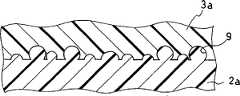
接着,讲述本发明的第3实施方式。图3是表示本实施方式中的粘接层和高强度层的界面的剖面图。如图3所示,在本实施方式中,在高强度层3a中的粘接层2a一侧的面上,形成细小的凹部9。该凹部9的深度为0.1~10μm,开口部的面积小于与内部中的高强度层3a的表面平行的剖面的面积,具有“罐子”状的形状。此外,高强度层3a中的粘接层2a一侧的面的十点的平均粗糙度,为1~5μm。然后,向该凹部9内注入形成粘接层2a的环氧树脂。Next, a third embodiment of the present invention will be described. Fig. 3 is a cross-sectional view showing the interface between the adhesive layer and the high-strength layer in the present embodiment. As shown in FIG. 3 , in the present embodiment, fine recesses 9 are formed on the surface of the high-strength layer 3 a on the side of the
下面,讲述本实施方式涉及的薄片材料的制造方法。首先,制造至少使单面成为粗糙面、表面形成凸部的铜箔。该凸部,例如在铜箔的表面,使铜再结晶后形成。然后,向该铜箔的表面涂敷液态的聚酰亚胺,使其硬化。这样,就制作出单面镶铜的聚酰亚胺薄膜。然后,采用湿腐蚀等手段,从该单面镶铜的聚酰亚胺薄膜上除去铜箔。这样,就能将铜箔的粗糙面写入聚酰亚胺薄膜的单面,能够形成表面具有凹部9的高强度层3a。接着,向高强度层3a上涂敷液态的环氧树脂。这时,环氧树脂浸入凹部9内。再接着,加热环氧树脂,使其热硬化。这样,就能制造出本实施方式涉及的薄片材料。本实施方式涉及的上述以外的结构,与前文讲述的第1实施方式一样。Next, a method of manufacturing the sheet material according to the present embodiment will be described. First, at least one surface of the copper foil is roughened and a convex portion is formed on the surface. The protrusions are formed, for example, on the surface of copper foil by recrystallizing copper. Then, liquid polyimide was applied to the surface of the copper foil and cured. In this way, a polyimide film with copper inlaid on one side is produced. Then, the copper foil is removed from the single-sided copper-laid polyimide film by means of wet etching or the like. In this way, the rough surface of the copper foil can be written on one surface of the polyimide film, and the high-strength layer 3 a having the concave portion 9 on the surface can be formed. Next, a liquid epoxy resin is applied to the high-strength layer 3a. At this time, the epoxy resin penetrates into the concave portion 9 . Next, heat the epoxy resin to make it thermally harden. In this way, the sheet material according to this embodiment can be manufactured. The configurations other than those described above in this embodiment are the same as those in the first embodiment described above.
如前所述,一般来说,聚酰亚胺等强度高的树脂,化学稳定性高,与粘接层之间的贴紧性差。与此不同,在采用上述结构的本实施方式的薄片材料及布线板中,由于在高强度层中的粘接层一侧的表面,形成细小的凹部,向该凹部内注入形成粘接层的树脂后形成凸部,所以可以获得由该凸部发挥的定位效果,高强度层和粘接层的贴紧性良好。这样,在本实施方式的薄片材料及布线板中,可以获得良好的可靠性。另外,在高强度层中的布线一侧的表面形成凹部后,在表皮效应的作用下,高频传输时的特性会稍稍下降。但布线一侧没有凹部时,就不存在这种问题。本实施方式中的上述以外的效果,与前文讲述的第1实施方式一样。As mentioned above, in general, high-strength resins such as polyimide have high chemical stability and poor adhesion to the adhesive layer. On the other hand, in the sheet material and the wiring board of the present embodiment having the above-mentioned structure, since fine recesses are formed on the surface of the high-strength layer on the side of the adhesive layer, the resin that forms the adhesive layer is injected into the recesses. The protrusions are formed after the resin, so the positioning effect exerted by the protrusions can be obtained, and the adhesion between the high-strength layer and the adhesive layer is good. In this way, good reliability can be obtained in the sheet material and the wiring board of the present embodiment. In addition, when recesses are formed on the surface of the wiring side in the high-strength layer, the characteristics at the time of high-frequency transmission are slightly lowered due to the skin effect. However, this problem does not exist when there is no recess on the wiring side. Effects other than those described above in this embodiment are the same as in the first embodiment described above.
此外,本第3实施方式可以与前文讲述的第2实施方式组合起来实施。即可以使用双面镶铜的聚酰亚胺薄膜,在高强度层中的两面形成细小的凹部。这样,与前文讲述的只在粘接层一侧的表面形成凹部时相比,虽然高频传输时的特性会稍稍下降,但在能够使高强度层和粘接层之间的贴紧性及高强度层和其它的薄片材料及布线的贴紧性得到提高的同时,还能获得采用消去法、添加法或半添加法可以轻易形成布线的薄片材料。另外,在前文讲述的第2及第3实施方式中,从镶铜的聚酰亚胺薄膜中除去铜箔后,复制铜箔的粗糙面,在高强度层的表面形成凹部。但本发明并不局限于此,可以采用其它方法形成凹部。In addition, this third embodiment can be implemented in combination with the second embodiment described above. That is, it is possible to form fine recesses on both sides of the high-strength layer by using a polyimide film inlaid with copper on both sides. In this way, compared with the case where the concave portion is formed only on the surface of the adhesive layer as described above, although the characteristics at the time of high-frequency transmission will be slightly lowered, the adhesion between the high-strength layer and the adhesive layer and the The adhesiveness of the high-strength layer and other sheet materials and wiring is improved, and it is possible to obtain a sheet material that can easily form wiring by a subtractive method, an additive method, or a semi-additive method. In addition, in the second and third embodiments described above, after the copper foil was removed from the copper-embedded polyimide film, the rough surface of the copper foil was copied to form the recesses on the surface of the high-strength layer. However, the present invention is not limited thereto, and other methods may be used to form the concave portion.
下面,讲述本发明的第4实施方式。在本实施方式中,对由聚酰亚胺构成的高强度层的表面实施表面处理。这时,有对高强度层中的与粘接层相接的一侧的面实施表面处理的情况和对与金属布线相接的一侧的面实施表面处理的情况。作为表面处理,有各种处理,例如紫外线照射处理、等离子体处理、离子束处理,碱处理等。Next, a fourth embodiment of the present invention will be described. In this embodiment, surface treatment is performed on the surface of the high-strength layer made of polyimide. In this case, surface treatment may be applied to the surface of the high-strength layer that is in contact with the adhesive layer, or surface treatment may be applied to the surface of the high-strength layer that is in contact with the metal wiring. As the surface treatment, there are various treatments such as ultraviolet irradiation treatment, plasma treatment, ion beam treatment, alkali treatment and the like.
在紫外线照射处理中,对紫外线的波长没有特别限定。但是采用照射波长为300nm以下的短波长的紫外线照射后,可以极大地改善高强度层和粘接层、其它的薄片材料或布线之间的贴紧性。作为这种紫外线光源,有UV灯泡及受激准分子灯泡等。作为受激准分子灯泡的示例,可以列举宇西欧电机制造的受激准分子VUU洗涤装置。该光源因型号而异,可以照射接近126nm、146nm、172nm、222nm、308nm的单波长的紫外线。此外,作为照射这种紫外线后提高贴紧性的原因,被认为是由于使表面的有机附着物分解后清净化、材料表面的化学反应等,但详细情况尚不明了。In the ultraviolet irradiation treatment, the wavelength of ultraviolet rays is not particularly limited. However, the adhesion between the high-strength layer and the adhesive layer, other sheet materials, or wiring can be greatly improved by irradiating with short-wavelength ultraviolet rays with an irradiation wavelength of 300 nm or less. Examples of such ultraviolet light sources include UV bulbs, excimer bulbs, and the like. As an example of an excimer light bulb, an excimer VUU washing device manufactured by Useo Electric can be cited. Depending on the model, this light source can irradiate single-wavelength ultraviolet rays near 126nm, 146nm, 172nm, 222nm, and 308nm. In addition, as the reason for the improvement of the adhesiveness after irradiation of such ultraviolet rays, it is considered that the organic deposits on the surface are decomposed and then cleaned, or a chemical reaction on the surface of the material, etc., but the details are not yet clear.
作为等离子体处理,向等离子体装置装入氧、氮或氟化氢等气体后,将该气体等离子化,对强度层进行腐蚀等表面处理。据认为高强度材料是聚酰亚胺时,效果特别显著。此外,在等离子体处理时导入的气体,并不局限于氧、氮或氟化氢等气体。As the plasma treatment, gas such as oxygen, nitrogen, or hydrogen fluoride is charged into a plasma device, and the gas is plasmaized to perform surface treatment such as etching on the strength layer. The effect is considered to be particularly pronounced when the high-strength material is polyimide. In addition, the gas introduced during the plasma treatment is not limited to gases such as oxygen, nitrogen, or hydrogen fluoride.
在离子束处理中,将离子束加速后照射到高强度层的表面。这样,如后文所述,由氟类聚合物构成高强度层时,可以获得与布线之间的良好的贴紧性。In ion beam processing, an ion beam is accelerated and irradiated onto the surface of the high-intensity layer. In this way, as will be described later, when the high-strength layer is made of a fluorine-based polymer, good adhesion to wiring can be obtained.
作为碱处理,有采用KOH、NaOH等水溶液的表面处理。高强度材料是聚酰亚胺时,使高强度层与强碱溶液接触后,聚酰亚胺的亚胺环开环,生成羧基及酰胺基。由于这些基的反应性强,所以可以在高强度层和粘接层、其它薄片材料或布线之间,获得很高的贴紧性。As the alkali treatment, there is surface treatment using an aqueous solution of KOH, NaOH or the like. When the high-strength material is polyimide, when the high-strength layer is brought into contact with a strong alkali solution, the imide rings of the polyimide are opened to form carboxyl groups and amide groups. Due to the high reactivity of these groups, very high adhesion can be obtained between the high-strength layer and the adhesive layer, other sheet materials or wiring.
这样,在本实施方式中,通过对高强度层的表面实施表面处理,从而可以提高高强度层和粘接层之间、高强度层和其它薄片材料之间、高强度层和金属布线之间的贴紧性。这样,还能在热循环试验之外,提高THB(steady-state Temperature Humidity Bias life test)及HAST(HighlyAccelerated Temperature and Humidity Stress Test)等的可靠性试验的评价结果。另外,对高强度层的表面实施表面处理时,由于在该表面形成的凹凸小到分子级或接近于它的程度,所以具有下述优点:在高强度层中的金属布线一侧的表面形成的凹凸,在高速传输中毫无问题。本实施方式中的上述以外的效果,与前文讲述的第1实施方式一样。Thus, in this embodiment, by performing surface treatment on the surface of the high-strength layer, the gap between the high-strength layer and the adhesive layer, between the high-strength layer and other sheet materials, and between the high-strength layer and metal wiring can be improved. of tightness. In this way, in addition to the thermal cycle test, the evaluation results of reliability tests such as THB (steady-state Temperature Humidity Bias life test) and HAST (Highly Accelerated Temperature and Humidity Stress Test) can be improved. In addition, when surface treatment is performed on the surface of the high-strength layer, since the unevenness formed on the surface is small at the molecular level or close to it, there is an advantage that the surface of the metal wiring side in the high-strength layer is formed. There is no problem in high-speed transmission. Effects other than those described above in this embodiment are the same as in the first embodiment described above.
此外,本实施方式中的表面处理,既可以实施上述处理中的某一个处理,也可以依次实施多个处理。In addition, in the surface treatment in this embodiment, one of the above-mentioned treatments may be performed, or a plurality of treatments may be performed sequentially.
下面,讲述本发明的第5实施方式。在本实施方式中,由液晶聚合体形成高强度层。作为液晶聚合体,是具有亚甲胺类、偶氮类、脂类、二苯乙烯类、联苯基类、联三苯类、二苯乙炔类、环己烷类、间而氮苯类、芴类、内元基、(硬直基)等的液晶聚合体。这些内元基,可以在聚合体的侧链上存在,但最好在主链上存在。此外,这些液晶聚合体也可以是多孔质体。本实施方式涉及的上述以外的结构,与前文讲述的第1实施方式一样。Next, a fifth embodiment of the present invention will be described. In this embodiment, the high-strength layer is formed of a liquid crystal polymer. As liquid crystal polymers, there are methyleneamines, azos, lipids, stilbenes, biphenyls, terphenyls, tolanylacetylenes, cyclohexanes, m-azobenzenes, Liquid crystal polymers of fluorenes, internal radicals, (hard straight radicals), etc. These internal groups can exist on the side chains of the polymer, but preferably exist on the main chain. In addition, these liquid crystal polymers may also be porous. The configurations other than those described above in this embodiment are the same as those in the first embodiment described above.
在如上结构的本实施方式的薄片材料及布线板中,作为形成高强度层的的高强度材料,使用液晶聚合体。这样,由于液晶聚合体具有分子次序的定向性,所以热膨胀系数小,能够制作具有接近于硅的热膨胀系数的材料,以及接近于形成布线的铜等金属的热膨胀系数的材料。例如,作为高强度层,制作具有接近于硅的热膨胀系数的材料后,布线板与半导体元件之间的热膨胀系数之差减小,外加热循环时,能够将热应力的产生抑制到很小的程度。另外,制作接近于金属的热膨胀系数的材料后,可以降低高强度层和布线之间的热应力。另外,液晶聚合体具有介电常数和介电损失小、吸水率小的特性,从这些方面说,也最好将液晶聚合体作为布线板材料。In the sheet material and the wiring board according to the present embodiment having the above configuration, a liquid crystal polymer is used as a high-strength material forming the high-strength layer. In this way, since the liquid crystal polymer has molecular order orientation, the thermal expansion coefficient is small, and a material having a thermal expansion coefficient close to that of silicon and a material close to that of metal such as copper forming wiring can be produced. For example, as a high-strength layer, after making a material with a thermal expansion coefficient close to that of silicon, the difference in thermal expansion coefficient between the wiring board and the semiconductor element is reduced, and the generation of thermal stress can be suppressed to a small amount during the external heating cycle. degree. In addition, by making a material with a thermal expansion coefficient close to that of metal, thermal stress between the high-strength layer and wiring can be reduced. In addition, liquid crystal polymers have the characteristics of low dielectric constant and dielectric loss, and low water absorption. From these points of view, liquid crystal polymers are also preferable as wiring board materials.
此外,作为布线板的绝缘膜,还考虑用单体使用液晶聚合体的方法。可是,由于具有焊锡耐热性等的液晶聚合体的软化点高(300℃左右),所以存在不能使用加热温度为200℃左右的普通的加热压力机的问题。另外,还存在软化时粘度急剧下降,所以层叠时难以控制的问题,和在多层布线化时,在上层挤压时的热量的作用下,已经制作好的下层由于软化而变形,所以难以多层布线化的问题。与此不同,在本实施方式中,只用液晶聚合体形成高强度层,使该高强度层与粘接层层叠后形成薄片材料,所以可以利用粘接层与基板或下层的薄片材料进行粘接,而不必将由液晶聚合体构成的高强度层加热到软化温度为止。因此,用单体使用液晶聚合体时,不会出现问题。In addition, as an insulating film of a wiring board, a method of using a liquid crystal polymer as a monomer is also conceivable. However, since the softening point of the liquid crystal polymer having solder heat resistance and the like is high (about 300°C), there is a problem that a general heating press with a heating temperature of about 200°C cannot be used. In addition, there is also the problem that the viscosity drops sharply when softening, so it is difficult to control when laminating, and when multilayer wiring is performed, under the action of heat when the upper layer is extruded, the lower layer that has already been produced is deformed due to softening, so it is difficult to do more. Layer routing issues. On the other hand, in this embodiment, only the liquid crystal polymer is used to form the high-strength layer, and the high-strength layer and the adhesive layer are laminated to form a sheet material, so the adhesive layer can be used to bond the substrate or the underlying sheet material. It is not necessary to heat the high-strength layer made of liquid crystal polymer to the softening temperature. Therefore, no problem occurs when the liquid crystal polymer is used as a monomer.
下面,讲述本发明的第6实施方式。在本实施方式中,利用使环氧树脂含有芳族聚酰胺纤维的复合材料形成粘接层。该复合材料中的芳族聚酰胺纤维的含有率,例如是10~50质量%。另外,作为高强度材料,使用液晶聚合体。本实施方式涉及的上述以外的结构,与前文讲述的第1实施方式一样。Next, a sixth embodiment of the present invention will be described. In this embodiment, the adhesive layer is formed using a composite material in which aramid fiber is contained in an epoxy resin. The content of the aramid fiber in the composite material is, for example, 10 to 50% by mass. In addition, as a high-strength material, a liquid crystal polymer is used. The configurations other than those described above in this embodiment are the same as those in the first embodiment described above.
在如上结构的本实施方式的薄片材料及布线板中,由于粘接层包含的芳族聚酰胺纤维本身具有抑制产生裂纹的效果,所以将该粘接层与高强度层组合后形成薄片材料时,可以获得更优异的耐裂纹性。另外,由于含有芳族聚酰胺纤维的热硬化树脂的热膨胀系数小,所以作为高强度材料使用液晶聚合体,作为热硬化材料使用含有芳族聚酰胺纤维的环氧树脂,从而可以使粘接层的热膨胀系数,与形成半导体元件的硅(Si)的热膨胀系数基本相等。其结果,即使外加热循环,也几乎产生热应力,所以可以制作不出现裂纹及挠曲的布线板。本实施方式涉及的上述以外的效果,与前文讲述的第1实施方式一样。In the sheet material and wiring board of the present embodiment having the above-mentioned structure, since the aramid fiber contained in the adhesive layer itself has the effect of suppressing cracks, when the sheet material is formed by combining the adhesive layer with the high-strength layer, , can obtain more excellent crack resistance. In addition, since the thermal expansion coefficient of thermosetting resin containing aramid fiber is small, liquid crystal polymer is used as a high-strength material, and epoxy resin containing aramid fiber is used as a thermosetting material, so that the adhesive layer can be made The coefficient of thermal expansion is substantially equal to the coefficient of thermal expansion of silicon (Si) forming semiconductor elements. As a result, thermal stress is almost generated even in an external heating cycle, so a wiring board free from cracks and warps can be produced. Effects other than those described above in this embodiment are the same as those in the first embodiment described above.
此外,在本实施方式中,热硬化性材料的矩阵,不限于环氧树脂,还可以使用其它的热硬化树脂。另外,作为热硬化性材料,可以代替含芳族聚酰胺纤维的热硬化树脂,使用含氟类聚合体。环氧树脂的介电常数及介电损耗通常稍大。但使用将介电常数低而且介电损耗低的树脂——氟素树脂分散的材料后,可以使这一点得到改善。作为这种材料,例如有使延伸PTFE含浸环氧树脂的材料(例如哥尔泰公司制造的maikuroramu600)。In addition, in this embodiment, the matrix of the thermosetting material is not limited to epoxy resin, and other thermosetting resins may be used. In addition, as the thermosetting material, instead of the thermosetting resin containing aramid fiber, a fluorine-containing polymer may be used. The dielectric constant and dielectric loss of epoxy resin are usually slightly higher. However, this can be improved by using a material in which fluororesin, a resin with low dielectric constant and low dielectric loss, is dispersed. As such a material, there is, for example, a material obtained by impregnating expanded PTFE with an epoxy resin (for example, maikuroramu 600 manufactured by Goltech Corporation).
另外,本实施方式中的热硬化树脂,考虑到在高频中使用布线板,最好是使用介电常数和介电损耗尽量低的材料。作为这种材料,除了环氧树脂外,还有聚烯及乙烯类树脂。另外,作为热硬化树脂,可以使用BT树脂。In addition, as for the thermosetting resin in this embodiment, it is preferable to use a material with a dielectric constant and a dielectric loss as low as possible in consideration of the use of a wiring board at high frequencies. Examples of such materials include polyolefin and vinyl resins in addition to epoxy resins. In addition, BT resin can be used as the thermosetting resin.
下面,讲述本发明的第7实施方式。在本实施方式中,由氟类聚合物形成高强度层。所谓“氟类聚合物”,是指分子结构内含氟原子的聚合物,例如:聚四氟乙烯、四氟合乙烯—全氟烷基乙烯醚共聚体、四氟合乙烯—乙烯共聚体、聚三氟氯乙烯、三氟氯乙烯—乙烯共聚体、聚偏氟乙烯、聚乙烯(基)等。此外,这些氟类聚合物,还可以是多孔质体。本实施方式涉及的上述以外的结构,与前文讲述的第1实施方式一样。Next, a seventh embodiment of the present invention will be described. In this embodiment, the high-strength layer is formed of a fluoropolymer. The so-called "fluorine polymers" refer to polymers containing fluorine atoms in the molecular structure, such as polytetrafluoroethylene, tetrafluoroethylene-perfluoroalkyl vinyl ether copolymer, tetrafluoroethylene-ethylene copolymer, Polychlorotrifluoroethylene, chlorotrifluoroethylene-ethylene copolymer, polyvinylidene fluoride, polyethylene (base), etc. In addition, these fluoropolymers may also be porous. The configurations other than those described above in this embodiment are the same as those in the first embodiment described above.
在如上结构的本实施方式的薄片材料及布线板中,由氟类聚合物形成高强度层。氟类聚合物的介电常数和介电损耗,在树脂中最低,是使用高频的高速传输布线板最理想的材料。另外,氟类聚合物虽然强度小,但延伸率极大,所以防止产生裂纹的效果大。但是,由于氟类聚合物是疏水性,所以与其它树脂层及金属布线的贴紧性低。因此,在由氟类聚合物构成的高强度层的表面,最好实施前文叙及的第4实施方式中的表面处理。In the sheet material and the wiring board of the present embodiment having the above configuration, the high-strength layer is formed of a fluorine-based polymer. Fluoropolymers have the lowest dielectric constant and dielectric loss among resins, making them ideal materials for high-frequency, high-speed transmission wiring boards. In addition, although fluoropolymers have low strength, they have extremely high elongation, so the effect of preventing cracks is large. However, since fluoropolymers are hydrophobic, they have low adhesion to other resin layers and metal wiring. Therefore, it is preferable to perform the surface treatment described above in the fourth embodiment on the surface of the high-strength layer made of a fluorine-based polymer.
下面,讲述本发明的第8实施方式。本实施方式涉及的薄片材料,与前文叙及的第1实施方式涉及的薄片材料1(参照图1)相同。在本实施方式中,在制作布线板之际,在金属板上形成薄片材料1,形成布线6a~6c及通路孔7后,腐蚀、除去金属板。这样,就制造出本实施方式涉及的布线板。Next, an eighth embodiment of the present invention will be described. The sheet material according to this embodiment is the same as the sheet material 1 (see FIG. 1 ) according to the first embodiment mentioned above. In this embodiment, when fabricating a wiring board, the sheet material 1 is formed on a metal plate to form the
本实施方式中,在制作布线板的工序中,由于在金属板上形成薄片材料1,所以金属板作为支持基板发挥作用,可以很容易地制造出平坦性优异的布线板。而且,最终除去金属板后,可以获得没有支持基板的非常薄的布线板。在这种薄型的布线板中,没有吸收热应力的支持基板,产生的应力全部集中到层叠的薄片材料中。因此,本发明的耐裂纹性良好的薄片材料特别有效。本实施方式涉及的上述以外的效果,与前文讲述的第1实施方式一样。In the present embodiment, since the sheet material 1 is formed on the metal plate in the process of producing the wiring board, the metal plate functions as a supporting substrate, and a wiring board excellent in flatness can be easily produced. Also, after finally removing the metal plate, a very thin wiring board without a supporting substrate can be obtained. In such a thin wiring board, there is no supporting substrate to absorb thermal stress, and all the stress generated is concentrated in the laminated sheet material. Therefore, the sheet material having excellent crack resistance of the present invention is particularly effective. Effects other than those described above in this embodiment are the same as those in the first embodiment described above.
此外,在本实施方式中,如前文讲述的第2~第4实施方式所示,最好在高强度层的表面,形成微小的凹部,或实施表面处理,提高和粘接层、其它薄片材料或布线的贴紧性。其理由是:本实施方式的布线板,由于没有吸收应力的支持基板,所以薄片材料的界面贴紧性差,容易产生界面剥离,使布线板的特性及可靠性下降。In addition, in this embodiment, as shown in the second to fourth embodiments described above, it is preferable to form minute recesses on the surface of the high-strength layer, or to perform surface treatment to improve the strength of the bonding layer and other sheet materials. Or the tightness of wiring. The reason is that the wiring board of this embodiment has no support substrate for absorbing stress, so the interface adhesion of the sheet material is poor, and interfacial peeling tends to occur, which reduces the characteristics and reliability of the wiring board.
下面,讲述前文所述的第8实施方式涉及的布线板的制造方法。图4(a)~(g),是按照其工序顺序表示本实施方式涉及的布线板的制造方法的剖面图。首先,如图4(a)所示,将粘接层2和高强度层3相互贴在一起后,制作薄片材料1。这时,粘接层2成为半硬化状态。Next, the method of manufacturing the wiring board according to the eighth embodiment described above will be described. 4( a ) to ( g ) are cross-sectional views showing the manufacturing method of the wiring board according to the present embodiment in order of the steps. First, as shown in FIG. 4( a ), after the
接着,如图4(b)所示,在金属板8上,形成布线6a。然后,在金属板8上配置薄片材料1,以便覆盖该布线6a。这时,薄片材料1的粘接层2与金属板8相接。这样,薄片材料1的粘接层2变形,埋入布线6a。再然后,加热,使粘接层2热硬化。Next, as shown in FIG. 4( b ), wiring 6 a is formed on
接着,如图4(c)所示,采用激光加工等方法,在薄片材料1中的布线6a的正上方的一部分区域形成通路孔11。接着,如图4(d)所示,将导体层埋入该通路孔11的内部,形成通路孔7。再接着,如图4(e)所示,在薄片材料1上形成布线6b。这时,布线6b通过通路孔7作媒介,与布线6a连接。Next, as shown in FIG. 4( c ), a via
接着,如图4(f)所示,在薄片材料1上层叠其它的薄片材料1(以下称作“薄片材料1a”),使其热硬化。这时薄片材料1a的粘接层2。埋入布线6b。接着,在薄片材料1a中的布线6b的正上方的一部分区域形成通路孔7。然后,在薄片材料1a上形成布线6c。这时,布线6c通过薄片材料1a中的通路孔7作媒介,与布线6b连接。Next, as shown in FIG. 4( f ), another sheet material 1 (hereinafter referred to as "
接着,如图4(g)所示,通过腐蚀除去金属板8。这样,第8实施方式涉及的布线板就制作了出来。Next, as shown in FIG. 4(g), the
此外,在图4(a)~(g)所示的制造方法中,作为支持基板使用了金属板8。但支持基板只要是具有平坦性的基板就行,并不需要特别限定金属板。另外,支持基板的除去方法也不局限于腐蚀,可以使用剥离等腐蚀以外的方法。In addition, in the manufacturing method shown in FIGS. 4( a ) to ( g ), a
另外,制作前文所述的第1实施方式涉及的布线板4时,在图4(a)~(f)所示的工具中,取代金属板8,在印刷基板上层叠薄片材料1及1a。然后,省略图4(g)所示的工序。这样,就能够制造出图2所示的布线板4。In addition, when manufacturing the wiring board 4 according to the first embodiment described above, in the jig shown in FIGS. Then, the steps shown in FIG. 4(g) are omitted. In this way, the wiring board 4 shown in FIG. 2 can be manufactured.
另外,在前文所述的第1~8实施方式中,取代热硬化树脂,可以使用热可塑性树脂。In addition, in the first to eighth embodiments described above, a thermoplastic resin may be used instead of a thermosetting resin.
以下,采用将本发明的实施示例与权利要求书的范围以外的比较示例进行比较的方式具体讲述。此外,本发明并不局限于以下的实施示例,在本发明的技术思想的范围内可以进行各种变形、变更。Hereinafter, a specific description will be made by comparing the embodiment examples of the present invention with comparative examples outside the scope of the claims. In addition, this invention is not limited to the following embodiment example, Various deformation|transformation and changes are possible within the range of the technical idea of this invention.
在以下所示的实施示例及比较示例中,制造形成高强度层的材料及表面状态不同的薄片材料时,对后文讲述的各实施示例及比较示例,分别使用该薄片材料,制作20个布线板的样品。然后,对其中的10个样品,在温度变化范围为-65~150℃中进行热循环试验,然后测量其布线电阻。对另外的10个样品,进行耐湿试验(HAST),经过所定的时间后,测量高强度层和粘接层之间的力学性的剥离强度及绝缘电阻。另外,还测量高强度层的抗拉强度。进而,对一部分实施示例测量高强度层和布线之间的抗剥离强度。In the examples of implementation and comparison examples shown below, when fabricating sheet materials with different materials and surface conditions for forming the high-strength layer, 20 wirings were produced using the sheet materials for each of the examples of implementation and comparison examples described later. Plate samples. Then, 10 of the samples were subjected to a thermal cycle test in a temperature range of -65 to 150° C., and then their wiring resistance was measured. The other 10 samples were subjected to a humidity resistance test (HAST), and after a predetermined period of time, the mechanical peel strength and insulation resistance between the high-strength layer and the adhesive layer were measured. In addition, the tensile strength of the high strength layer was also measured. Furthermore, the peeling resistance between the high-strength layer and the wiring was measured for a part of the implementation examples.
下面,讲述热循环试验及耐湿试验的目的及详细的试验方法。如果在在实际使用条件(25~70℃)中评价半导体器件的热应力耐久性,评价就相当费时。因此,对样品外加(-65~150℃)的热循环,进行加速试验。就是说,外加将在-65℃的温度中保持30分钟后再在+150℃的温度中保持30分钟的基本循环反复进行所定次数的热循环。此外,从低温(-65℃)到高温(+150℃)移行的移行时间及从高温到低温移行的移行时间,因热循环试验机的能力及样品的热容量而异,所以要适当调整。假设在热循环试验中,由于热应力在绝缘膜中产生裂纹,该裂纹切断布线板的布线,那么所述布线电阻就要比热循环试验前增大。因此,测量布线电阻后,能够评价布线板的可靠性。Next, the purpose and detailed test methods of the thermal cycle test and the humidity resistance test will be described. If the thermal stress durability of a semiconductor device is evaluated under actual use conditions (25 to 70° C.), the evaluation takes a considerable amount of time. Therefore, a thermal cycle (-65 to 150° C.) was applied to the sample to perform an accelerated test. That is, the basic cycle of holding at a temperature of -65°C for 30 minutes followed by holding at a temperature of +150°C for 30 minutes is repeated for a given number of thermal cycles. In addition, the transition time from low temperature (-65°C) to high temperature (+150°C) and the transition time from high temperature to low temperature vary depending on the capability of the thermal cycle tester and the heat capacity of the sample, so appropriate adjustments should be made. Assuming that in the thermal cycle test, a crack is generated in the insulating film due to thermal stress, and the crack cuts the wiring of the wiring board, the wiring resistance is increased compared to before the thermal cycle test. Therefore, after measuring the wiring resistance, the reliability of the wiring board can be evaluated.
另外,如前所述,聚酰亚胺等的高强度材料因其化学稳定性高,所以与其它材料的贴紧性及粘接性往往较低。将这种贴紧性及粘接性较低的材料与其它材料层叠时,两种材料的界面的强度就不够。这种不够的粘接强度虽然也能原封不动地进行评价,但放置样品的环境存在极性很高的水时,这种水容易浸入粘接较弱的界面,在使该界面的粘接强度进一步降低的同时,还使绝缘电阻降低。所以,在高湿高温下,长时间置放样品后,就能够更明确地检出粘接强度是否足够。作为这种试验,可以列举HAST(High1yAccelerated Temperature and Humidity Stress Test、标准:JESD22-A110-B)及THB(steady-state Temperature Humidity Bias life test、标准:JESD22-A110-B)。此外,试验标准JESD,是指“JEDEC Standards”;JEDEC表示Joint Electron Device Engineering Council(美国电子器件的有关标准化团体;网址http://www·jedec·org)。Also, as mentioned above, high-strength materials such as polyimide tend to have low adhesion and adhesiveness to other materials due to their high chemical stability. When such a material with low adhesiveness and adhesiveness is laminated with another material, the strength of the interface between the two materials is insufficient. Although such insufficient adhesive strength can be evaluated as it is, if there is highly polar water in the environment where the sample is placed, this water will easily infiltrate into the interface with weak adhesion, and the adhesion of the interface will be reduced. While the strength is further reduced, the insulation resistance is also reduced. Therefore, after placing the sample for a long time under high humidity and high temperature, it is possible to more clearly detect whether the adhesive strength is sufficient. Examples of such tests include HAST (High Accelerated Temperature and Humidity Stress Test, standard: JESD22-A110-B) and THB (steady-state Temperature Humidity Bias life test, standard: JESD22-A110-B). In addition, the test standard JESD refers to "JEDEC Standards"; JEDEC means Joint Electron Device Engineering Council (the relevant standardization body for electronic devices in the United States; website http://www.jedec.org).
下面,详细讲述各实施示例及比较示例Next, each implementation example and comparison example will be described in detail.
(实施示例1)(implementation example 1)
作为高强度材料,使用双面镶铜的聚酰亚胺薄膜(宇部兴产制ユピセルN、铜箔厚度:12μm、聚酰亚胺厚度:25μm)。用碱铜腐蚀液溶解双面镶铜的聚酰亚胺薄膜的双面的铜箔。使用扫描型电子显微镜(SEM),观察铜箔腐蚀后的聚酰亚胺薄膜的表面后,可以看到写入铜箔的粗糙面后形成的细小的凹部。As a high-strength material, a polyimide film (upisel N manufactured by Ube Industries, Copper Foil Thickness: 12 μm, Polyimide Thickness: 25 μm) was used with double-sided copper inlaid. Dissolve the copper foil on both sides of the polyimide film with copper inlaid on both sides with alkaline copper etching solution. When the surface of the polyimide film after the copper foil was etched was observed using a scanning electron microscope (SEM), fine recesses formed by writing on the rough surface of the copper foil were observed.
接着,将腐蚀了铜箔的聚酰亚胺薄膜和半硬化状态(B等级)的环氧树脂材料(味之素制ABF、厚度:40μm)加热到80℃后,采用真空叠片法粘贴到一起,作为薄片材料。另一方面,在铜板上形成作为腐蚀阻挡层的Ni电镀层,在该腐蚀阻挡层上,形成由金属层及铜层的2层膜构成的BGA岛部。然后,在该铜板上层叠挤压所述薄片材料,在170℃的温度中保持60分钟,使环氧树脂硬化。切出在该铜板上形成的一部分薄片材料,观察其截面。Next, heat the polyimide film etched with the copper foil and the epoxy resin material (ABF manufactured by Ajinomoto, thickness: 40 μm) in a semi-cured state (B grade) to 80°C, and then stick them on by the vacuum lamination method. together, as sheet material. On the other hand, a Ni plating layer was formed as a corrosion barrier layer on the copper plate, and a BGA island portion composed of a two-layer film of a metal layer and a copper layer was formed on the corrosion barrier layer. Then, the sheet material was laminated and extruded on the copper plate, and kept at a temperature of 170° C. for 60 minutes to harden the epoxy resin. A part of the sheet material formed on the copper plate was cut out, and its cross section was observed.
图5是表示薄片材料中的聚酰亚胺层和环氧树脂层的界面的截面光学显微镜照片。此外,在图5中示出刻度,该刻度的最小单位是1μm。如图5所示,在作为高强度层的聚酰亚胺层13作为粘接层的环氧树脂层12中,在聚酰亚胺层13的表面,形成罐子状的凹部14,环氧树脂流入该凹部14中,环氧树脂层12成为咬入聚酰亚胺层13的结构。在这种状态下,想将聚酰亚胺层13和环氧树脂层12互相分离,但两者却牢固地贴在一起,无法分离。5 is a cross-sectional optical micrograph showing the interface between a polyimide layer and an epoxy resin layer in a sheet material. In addition, a scale is shown in FIG. 5 , and the minimum unit of the scale is 1 μm. As shown in FIG. 5 , in the
接着,用二氧化碳激光在该铜板上形成通路孔后,进行去污(デスミア)处理,实施以钯为催化剂的无电解电镀。其结果,在与电镀液相接的薄片的表面及通路孔的侧面形成均匀的无电解电镀层。使用电镀抗蚀剂,在形成无电解电镀层的试料上形成图案,经过电镀后,在形成厚约18μm的布线的同时,还电镀充填通路孔。接着,经过腐蚀,有选择地除去不需要的无电解电镀层。Next, via holes were formed on the copper plate with a carbon dioxide laser, desmia treatment was performed, and electroless plating using palladium as a catalyst was performed. As a result, a uniform electroless plating layer is formed on the surface of the sheet in contact with the plating solution and the side surfaces of the via holes. Using a plating resist, a pattern was formed on a sample on which an electroless plating layer was formed, and after plating, wiring was formed with a thickness of about 18 μm, and via holes were also plated and filled. Next, through etching, unnecessary electroless plating is selectively removed.
反复进行上述工序后,就制作出多层布线板。接着,在该布线板上,用倒装片连接搭载测试用的半导体元件。然后,腐蚀、除去下层的铜板,接着还除去腐蚀阻挡层——Ni层。经过以上工序后,就得到搭载半导体元件的布线板。此外,在制造的布线板中,在没有搭载半导体元件的区域,设置了设置着HAST试验用的通路孔和布线的TEG(测试元件组)。After the above steps are repeated, a multilayer wiring board is produced. Next, on this wiring board, a semiconductor element for testing is mounted by flip-chip connection. Then, the copper plate of the lower layer is etched and removed, and then the corrosion barrier layer—the Ni layer is also removed. After the above steps, a wiring board on which semiconductor elements are mounted is obtained. In addition, in the manufactured wiring board, a TEG (Test Element Group) in which via holes and wiring for the HAST test are provided is provided in an area where no semiconductor element is mounted.
在该布线板的BGA岛部上搭载焊锡点后,将半导体元件逐一切断,作为试验样品。使用10个这种试验样品,进行了温度变化范围为-65~150℃的热循环试验。其结果,经过1000个热循环后,也没有发生布线电阻因断线等而增大的现象。After mounting solder bumps on the BGA islands of this wiring board, the semiconductor elements were cut one by one to obtain test samples. Using 10 of these test samples, a heat cycle test was performed in a temperature range of -65 to 150°C. As a result, even after 1000 thermal cycles, the wiring resistance did not increase due to disconnection or the like.
对另外10个样品进行了HAST试验(温度:130℃、温度:85%RH、外加电压:5V)。对通路孔间的绝缘电阻进行了HAST试验(通路孔/岛直径:90/150μm、通路孔间距:300μm)。在HAST试验中,经过400小时后,也没有出现绝缘电阻值的下降等问题。另外,对HAST试验后的样品,试着使聚酰亚胺层和环氧树脂层分离。但两者相互牢固地紧贴在一起,没有能够分离。A HAST test (temperature: 130° C., temperature: 85% RH, applied voltage: 5 V) was performed on the other 10 samples. A HAST test was performed on the insulation resistance between via holes (via hole/island diameter: 90/150 μm, via hole pitch: 300 μm). In the HAST test, there was no problem such as a decrease in the insulation resistance value even after 400 hours had elapsed. In addition, for the sample after the HAST test, it was attempted to separate the polyimide layer and the epoxy resin layer. But the two are firmly attached to each other and cannot be separated.
通过电镀对形成无电解电镀层的其它铜板上的薄片材料实施板电镀,形成厚约18μm的铜层。将该铜层留下宽度为10mm的矩形后,除去剩余部分,测量了90度抗剥离强度(抗剥强度,遵照JIS C6481)。抗剥离强度是1.5KN/m。Plate plating was performed on the sheet material on another copper plate forming the electroless plated layer by electroplating to form a copper layer having a thickness of about 18 μm. After leaving the copper layer in a rectangle with a width of 10 mm, the remaining part was removed, and the 90-degree peel strength was measured (peel strength, in accordance with JIS C6481). The peel strength is 1.5KN/m.
另外,将使用了铜箔腐蚀后的聚酰亚胺薄膜切出宽度为10mm的矩形后,进行了抗拉试验。抗拉试验遵照《JPCA标准组合布线板JPCA-BU01》。其结果,断裂延伸为78%(温度:23℃℃)、抗拉强度为450MPa(温度:23℃)、480MPa(温度:-65℃)、350MPa(温度:150℃)。所以,前文叙及的(a/b)比、即温度为-65℃时的抗拉断裂强度a和温度为150℃时的抗拉断裂强度b之比,是1.37。Moreover, the tensile test was done after cutting out the polyimide film etched using the copper foil into a rectangle with a width of 10 mm. The tensile test complies with the "JPCA Standard Combined Wiring Board JPCA-BU01". As a result, the elongation at break was 78% (temperature: 23°C), and the tensile strength was 450 MPa (temperature: 23°C), 480 MPa (temperature: -65°C), and 350 MPa (temperature: 150°C). Therefore, the aforementioned (a/b) ratio, that is, the ratio of the tensile breaking strength a at a temperature of -65°C to the tensile breaking strength b at a temperature of 150°C, is 1.37.
(实施示例2)(implementation example 2)
用保护薄膜盖住双面镶铜的聚酰亚胺薄膜的单面,使用和实施示例1一样腐蚀液,只除去其单面的铜箔。另外,该聚酰亚胺薄膜的厚度及机械特性,和前文讲述的实施示例1相同。在腐蚀了聚酰亚胺薄膜中的铜箔的一侧的面上,将半硬化状态的环氧树脂(日本油漆制プロビユ一ト、厚度:50μm)真空叠片后,获得叠层薄片材料。Cover one side of the polyimide film with double-sided copper inlaid with a protective film, use the same etching solution as in Example 1, and only remove the copper foil on one side. In addition, the thickness and mechanical properties of the polyimide film are the same as those of Embodiment 1 described above. A laminated sheet material was obtained by vacuum laminating a semi-hardened epoxy resin (Project, thickness: 50 μm) in a semi-hardened state on the surface of the polyimide film on which the copper foil was etched.
将该叠层材料,层叠挤压到和实施示例1一样的铜板上,获得在铜板上形成的薄片材料。接着,在其剩下的一侧的铜箔上布图,采用消去法形成布线。再接着搭载半导体元件,腐蚀、除去铜板后,就制作出布线板。The laminated material was stacked and extruded onto the same copper plate as in Example 1 to obtain a sheet material formed on the copper plate. Next, a pattern is patterned on the copper foil on the remaining side, and wiring is formed by the erasing method. Next, semiconductor elements are mounted, and the copper plate is etched and removed to produce a wiring board.
在本实施方式中,和实施示例1一样,采用使环氧树脂层咬入聚酰亚胺薄膜的表面凹部的结构,使两者不能离开。In the present embodiment, as in Embodiment 1, the structure in which the epoxy resin layer bites into the concave portion of the surface of the polyimide film is adopted so that both cannot separate.
另外,和实施示例1一样,进行了热循环试验及HAST试验。经过1000个热循环后,也没有发生布线电阻因断线等而增大的现象;在经过400小时的HAST试验后,也没有出现绝缘电阻值的下降等问题。另外,对HAST试验后的样品,试着使聚酰亚胺薄膜—环氧树脂层分离。但两者相互牢固地紧贴在一起,没有能够分离。In addition, as in Example 1, a heat cycle test and a HAST test were performed. After 1,000 thermal cycles, there was no increase in wiring resistance due to disconnection, etc.; after 400 hours of HAST testing, there was no decrease in insulation resistance. In addition, for the sample after the HAST test, it was attempted to separate the polyimide film-epoxy resin layer. But the two are firmly attached to each other and cannot be separated.
在上述实施示例1及2中,讲述了对在金属板上制作、最后除去金属板的布线板的实施示例。这是因为最后除去金属板、只具有由薄片材料构成的绝缘膜和金属布线的布线板,与具有板芯基板的布线板相比,搭载半导体元件等时产生的热应力的影响大。就是说,必须产生的热应力由薄薄的绝缘膜吸收,所以要求绝缘膜的断裂强度大。这就意味着,如果是可以在最后除去金属板的布线板中使用的材料,那么在印刷布线板等具有板芯基板的布线板中也能使用。可是,在印刷布线板等具有板芯基板的布线板中,线膨胀系数也和薄片材料不同,在搭载的半导体元件的插脚数量较多时,有可能以薄片材料和金属布线及其它不同的材料的界面为起点,产生裂纹,因此,本发明所示的这种耐裂纹性高的薄片材料是有效的。下面,作为实施示例3,讲述具有印刷基板的布线板。In the above Embodiments 1 and 2, the embodiment of the wiring board which is fabricated on a metal plate and finally removed from the metal plate has been described. This is because a wiring board having only an insulating film made of a thin sheet material and metal wiring without the metal plate at the end is more affected by thermal stress generated when semiconductor elements are mounted than a wiring board having a core substrate. That is, the thermal stress that must be generated is absorbed by the thin insulating film, so the breaking strength of the insulating film is required to be large. This means that if it is a material that can be used in a wiring board from which the metal plate is removed last, it can also be used in a wiring board having a core substrate such as a printed wiring board. However, in a wiring board with a core substrate such as a printed wiring board, the linear expansion coefficient is also different from that of the sheet material, and when the number of pins of the mounted semiconductor element is large, it may be possible to use the sheet material, metal wiring, or other different materials. The interface is the starting point, and cracks are generated, so the sheet material with high crack resistance shown in the present invention is effective. Next, as
(实施示例3)(implementation example 3)
将和实施示例1一样制作的层叠薄片材料,层叠挤压到具有印刷布线的FR-4基板上,在170℃的温度中保持80分钟后,使下层的环氧树脂硬化,与FR-4基板粘接。切出含有该FR-4基板的层叠材料中的-部分,观察其截面,可以看到环氧树脂层咬入聚酰亚胺薄膜的凹部的结构。在这种种状态下,试着使聚酰亚胺层和环氧树脂层分离。但两者相互牢固地紧贴在一起,没有能够分离。The laminated sheet material produced in the same way as in Example 1 is laminated and extruded onto the FR-4 substrate with printed wiring, and after being kept at a temperature of 170°C for 80 minutes, the epoxy resin of the lower layer is hardened, and the FR-4 substrate bonding. A part of the laminated material including this FR-4 substrate was cut out, and its cross-section was observed, and a structure in which the epoxy resin layer bit into the concave portion of the polyimide film was seen. In these states, try to separate the polyimide layer and the epoxy resin layer. But the two are firmly attached to each other and cannot be separated.
用激光在FR-4基板上的层叠材料中形成通路孔后,进行去污(デスミア)处理,实施以钯为催化剂的无电解电镀。从而在薄片材料的上面及通路孔部的内面形成由无电解电镀层构成的电镀基底层。Via holes are formed in the laminated material on the FR-4 substrate by laser, followed by desmia treatment and electroless plating using palladium as a catalyst. Accordingly, a plating base layer composed of an electroless plating layer is formed on the upper surface of the sheet material and the inner surface of the via hole portion.
接着,使用抗蚀剂,在形成电镀基底层的试料上形成布线图案,进行电镀,除去抗蚀剂,在形成所需的图案的布线的同时,还电镀充填通路孔内。布线的厚度调整为约18μm。然后,有选择地除去不需要的无电解电镀层。Next, using a resist, a wiring pattern is formed on the sample on which the plating base layer is formed, plating is performed, the resist is removed, and the wiring of a desired pattern is formed, and the inside of the via hole is also plated and filled. The thickness of the wiring was adjusted to about 18 μm. Then, the unnecessary electroless plating layer is selectively removed.
反复进行上述工序后,就制作出多层基板。接着,在该多层基板上,用倒装片连接搭载半导体元件。这样,就得到搭载半导体元件的布线板。After the above steps are repeated, a multilayer substrate is produced. Next, semiconductor elements are mounted on the multilayer substrate by flip-chip connection. In this way, a wiring board on which a semiconductor element is mounted is obtained.
按照半导体元件切断该多层布线板,作为试验样品。使用20个这种试验样品,进行了热循环试验(-65~150℃)。经过1000个热循环后,也没有发生断线等问题。This multilayer wiring board was cut according to a semiconductor element and used as a test sample. Using 20 of these test samples, a thermal cycle test (-65 to 150° C.) was performed. After 1000 thermal cycles, there were no problems such as disconnection.
(实施示例4)(implementation example 4)
作为热硬化树脂,使用了将芳族聚酰胺纤维作为加强基材,将环氧树脂作为矩阵的半硬化的热硬化材料(新神户电极制EA541、芳族聚酰胺纤维含有率30质量%)。除此之外,采用和实施示例1同样的方法,制造布线板。就是说,本实施示例使用的聚酰亚胺薄膜,和前文讲述的实施示例1中使用的聚酰亚胺薄膜一样。As the thermosetting resin, a semi-cured thermosetting material (EA541 manufactured by Shin-Kobe Electrode Co., Ltd., 30% by mass of aramid fiber content) having aramid fiber as a reinforcing base material and an epoxy resin as a matrix was used. Other than that, in the same manner as in Embodiment Example 1, a wiring board was produced. That is, the polyimide film used in this embodiment example is the same as the polyimide film used in Embodiment Example 1 described above.
在本实施示例的布线板中,也采用使粘界层咬入聚酰亚胺层的凹部的结构,使两者不能离开。另外,热循环试验也经过1000个热循环后,没有发生断线等问题;在经过400小时的HAST试验后,也没有出现绝缘电阻值的下降等问题。Also in the wiring board of this embodiment example, a structure is employed in which the interface layer bites into the concave portion of the polyimide layer so that both cannot separate. In addition, after 1,000 thermal cycles in the thermal cycle test, there were no problems such as disconnection; after 400 hours of the HAST test, there was no problem such as a drop in insulation resistance.
(实施示例5)(implementation example 5)
作为热硬化性树脂,使用由使延伸多孔质氟类聚合物(聚四氟乙烯)含浸环氧树脂、由半硬化的热硬化性材料构成的热硬化性材料(哥尔泰制マイクロラム600、氟类聚合物含有率25%),制作布线板。本实施示例的布线板中上述以外的结构,和前文讲述的实施示例1一样。就是说,本实施示例使用的聚酰亚胺薄膜,和前文讲述的实施示例1中使用的聚酰亚胺薄膜一样。As the thermosetting resin, a thermosetting material made of a semi-cured thermosetting material (Microlam 600, manufactured by Galtech, Inc.) was used by impregnating an extended porous fluoropolymer (polytetrafluoroethylene) with an epoxy resin. Fluoropolymer content rate 25%), a wiring board was produced. The configuration other than the above in the wiring board of this embodiment example is the same as that of Embodiment 1 described above. That is, the polyimide film used in this embodiment example is the same as the polyimide film used in Embodiment Example 1 described above.
在本实施示例的布线板中,也采用使粘界层咬入聚酰亚胺层的凹部的结构,使两者不能离开。另外,热循环试验也经过1000个热循环后,没有发生断线等问题。Also in the wiring board of this embodiment example, a structure is employed in which the interface layer bites into the concave portion of the polyimide layer so that both cannot separate. In addition, in the heat cycle test, after 1,000 heat cycles, no problems such as disconnection occurred.
(实施示例6)(implementation example 6)
作为包含二苯甲酮骨架的聚酰亚胺,利用棒状涂料器将聚[N,N’(1,4苯撑)-3,3’4,4—二苯甲酮4羧基亚胺](アルドリッチ试药)涂敷到PTFE上,使其干燥后形成聚酰亚胺薄膜。然后,将聚酰亚胺薄膜从PTFE上剥离。这样,就得到第2层使用的包含二苯甲酮骨架的聚酰亚胺薄膜(薄膜厚度:20μm)。将得到的聚酰亚胺薄膜,两面是平坦的。该聚酰亚胺薄膜和半硬化状态的环氧树脂(味之素制ABF、厚度:40μm)加热到80℃的温度后,采用真空叠片的方法贴在一起,作为薄片材料。从该薄片材料中采取样品,供做聚酰亚胺层和环氧树脂层之间的抗剥离强度试验、热循环试验及HAST试验、聚酰亚胺层和布线之间的抗剥离强度试验、聚酰亚胺薄膜的抗拉试验。As a polyimide containing a benzophenone skeleton, poly[N,N'(1,4phenylene)-3,3'4,4-benzophenone 4 carboxyimide]( Aldrich reagent) is coated on PTFE and dried to form a polyimide film. Then, the polyimide film was peeled off from the PTFE. In this way, a polyimide film (film thickness: 20 μm) containing a benzophenone skeleton used for the second layer was obtained. Both surfaces of the obtained polyimide film were flat. This polyimide film and a semi-hardened epoxy resin (ABF manufactured by Ajinomoto, thickness: 40 μm) were heated to a temperature of 80° C. and bonded together by vacuum lamination to form a sheet material. Samples are taken from the sheet material for the peel strength test between the polyimide layer and the epoxy resin layer, the thermal cycle test and the HAST test, the peel strength test between the polyimide layer and the wiring, Tensile test of polyimide film.
在聚酰亚胺层和环氧树脂层之间的抗剥离强度试验中,在该铜板上层叠挤压所述薄片材料,在170℃的温度中保持60分钟,使环氧树脂硬化。然后,采用和实施实例1同样的方法,测量聚酰亚胺层和环氧树脂层之间的抗剥离强度。但两者却牢固地贴在一起,无法分离。In the peel strength test between the polyimide layer and the epoxy resin layer, the sheet material was laminated and extruded on the copper plate, and kept at a temperature of 170° C. for 60 minutes to harden the epoxy resin. Then, using the same method as in Example 1, the peel strength between the polyimide layer and the epoxy resin layer was measured. But the two are firmly attached together and cannot be separated.
另一方面,在热循环试验及HAST试验中,和实施实例1同样,在铜板上形成BGA岛部,在该铜板上层叠挤压所述叠片后的薄片材料,在170℃的温度中保持60分钟,使环氧树脂硬化,得到由铜板上形成的薄片材料构成的绝缘膜。然后,通过溅射,在该绝缘膜上形成金属层。此外,该金属层是由贴紧用的下层和由铜构成的上层的2层膜。接着,将该金属层作为晶种层,实施无电解电镀,形成布线。然后,采用和前文叙及的实示施例1同样的方法,制作搭载半导体元件的布线板,将焊锡点搭载到BGA岛部上。On the other hand, in the thermal cycle test and the HAST test, as in Example 1, a BGA island was formed on a copper plate, and the laminated sheet material was laminated and extruded on the copper plate, and kept at a temperature of 170°C. For 60 minutes, the epoxy resin was cured to obtain an insulating film composed of the flake material formed on the copper plate. Then, a metal layer is formed on the insulating film by sputtering. In addition, this metal layer is a two-layer film consisting of a lower layer for adhesion and an upper layer made of copper. Next, using this metal layer as a seed layer, electroless plating is performed to form wiring. Then, a wiring board on which a semiconductor element is mounted was produced by the same method as in the first exemplary embodiment described above, and solder dots were mounted on the BGA islands.
接着,按照半导体元件,切断该布线板,作为试验样品。然后,和实示施例1一样,进行热循环试验及HAST试验。其结果,在热循环试验中,经过800个热循环后,也没有发生布线电阻因断线等而增大的现象;在HAST试验中,经过400小时后,也没有出现绝缘电阻值的下降等问题。另外,对HAST试验后的样品,试着使聚酰亚胺薄膜和环氧树脂层分离。但两者相互牢固地紧贴在一起,没有能够分离。Next, according to the semiconductor element, this wiring board was cut, and it was set as a test sample. Then, as in Example 1, a thermal cycle test and a HAST test were performed. As a result, in the thermal cycle test, there was no increase in wiring resistance due to disconnection after 800 thermal cycles; in the HAST test, there was no decrease in insulation resistance after 400 hours. question. In addition, for the sample after the HAST test, it was attempted to separate the polyimide film and the epoxy resin layer. But the two are firmly attached to each other and cannot be separated.
进而,在聚酰亚胺层和布线之间的抗剥离试验中,和实示施例1一样,在铜板上层叠所述薄片材料,在170℃的温度中保持60分钟,使其硬化。然后,采用溅射法贴附铜的薄膜,将它作为晶种层进行电镀,形成厚约18μm的铜箔。然后,采用和实示施例1一样的方法,测量的结果是抗剥离强度为1.2KN/m。Furthermore, in the peeling resistance test between the polyimide layer and the wiring, as in Example 1, the sheet material was stacked on a copper plate, and it was cured at a temperature of 170° C. for 60 minutes. Then, a copper thin film was attached by sputtering, and it was plated as a seed layer to form a copper foil with a thickness of about 18 μm. Then, using the same method as in Example 1, the result of measurement was that the peel strength was 1.2 KN/m.
将使用了包含二苯甲酮骨架的聚酰亚胺薄膜切出宽度为10mm的矩形后,进行了抗拉试验。断裂延伸为19%(温度:23℃°)、抗拉强度为170MPa(温度:23℃)、190MPa(温度:-65℃)、79MPa(温度:150℃)。所以,所述(a/b)比是2.41。The tensile test was performed after cutting out the polyimide film containing a benzophenone skeleton into a rectangle with a width of 10 mm. The elongation at break is 19% (temperature: 23°C), and the tensile strength is 170MPa (temperature: 23°C), 190MPa (temperature: -65°C), and 79MPa (temperature: 150°C). Therefore, the (a/b) ratio is 2.41.
(实示施例7)(Example 7)
作为高强度材料,使用单面形成铜箔的带铜箔的液晶聚合物(新日铁化学制エスパネツクス)。液晶聚合物层的膜厚是25μm,铜箔的膜厚是18μm。除此之外,采用和实示施例1同样的方法,制作布线板,进行了试验。在热循环试验中,经过900个热循环后,也没有发生布线电阻因断线等而增大的现象;在HAST试验(温度:120℃、湿度:85%RH)中,经过400小时后,也没有问题。铜箔的抗剥离强度为1.2KN/m。As a high-strength material, a copper-foiled liquid crystal polymer (Espanex, manufactured by Nippon Steel Chemical Co., Ltd.) with copper foil formed on one side was used. The film thickness of the liquid crystal polymer layer was 25 μm, and the film thickness of the copper foil was 18 μm. Other than that, by the same method as in Example 1, a wiring board was fabricated and tested. In the thermal cycle test, after 900 thermal cycles, the wiring resistance did not increase due to disconnection, etc.; in the HAST test (temperature: 120°C, humidity: 85%RH), after 400 hours, No problem either. The peel strength of copper foil is 1.2KN/m.
测量了除去铜箔后的液晶聚合物层的抗拉断裂强度,结果是:断裂延伸为28%(温度:23℃℃)、抗拉拉断强度为190MPa(温度:23℃)、230MPa(温度:-65℃)、120MPa(温度:150℃)。所以,所述(a/b)比是1.92。The tensile breaking strength of the liquid crystal polymer layer after removing the copper foil was measured, and the results were: the elongation at break was 28% (temperature: 23°C), the tensile breaking strength was 190MPa (temperature: 23°C), 230MPa (temperature : -65°C), 120MPa (temperature: 150°C). Therefore, the (a/b) ratio is 1.92.
(实示施例8)(Example 8)
作为高强度材料,准备了聚酰亚胺薄膜(宇部兴产制ユ一ピレックス、厚度:25μm)。将该聚酰亚胺薄膜切出宽度为1cm的矩形后,进行了抗拉试验。其结果是:断裂延伸为120%(温度:23℃℃)、抗拉强度为270MPa(温度:23℃)、310MPa(温度:-65℃)、210MPa(温度:150℃)。所以,所述(a/b)比是1.48。A polyimide film (upilex manufactured by Ube Industries, thickness: 25 μm) was prepared as a high-strength material. This polyimide film was cut out into a rectangle with a width of 1 cm, and then a tensile test was performed. As a result, the elongation at break was 120% (temperature: 23°C), and the tensile strength was 270MPa (temperature: 23°C), 310MPa (temperature: -65°C), and 210MPa (temperature: 150°C). Therefore, the (a/b) ratio is 1.48.
准备3块前文讲述的聚酰亚胺薄膜,对其中1块实施紫外线照射处理,对另1块实施等离子体处理,对剩下的一块不进行处理。然后,分别将半硬化状态的环氧树脂(味之素制ABF)真空叠片到这些聚酰亚胺薄膜上,获得叠层薄片材料。紫外线照射处理,用受激准分子UV灯泡(宇西欧电机制、中心波长:172nm)照射2分钟。在等离子体处理中,利用温度为45℃的氧等离子体处理3分钟。然后,分别从如此制成的3种薄片材料中切出样品,供做聚酰亚胺层—环氧树脂层之间的抗剥离强度试验、热循环可靠性试验布线—聚酰亚胺层之间的抗剥离强度试验。Three polyimide films described above were prepared, one of which was subjected to ultraviolet irradiation treatment, the other was subjected to plasma treatment, and the remaining one was not treated. Then, semi-cured epoxy resin (ABF manufactured by Ajinomoto Co., Ltd.) was vacuum-laminated on each of these polyimide films to obtain a laminated sheet material. For ultraviolet irradiation treatment, irradiate for 2 minutes with an excimer UV bulb (Usio Denki, center wavelength: 172 nm). In the plasma treatment, oxygen plasma at a temperature of 45° C. was used for 3 minutes. Then, samples were cut out from the three kinds of sheet materials thus prepared for the peel strength test between the polyimide layer and the epoxy resin layer, and the thermal cycle reliability test between the wiring and the polyimide layer. Peel strength test between.
在聚酰亚胺层—环氧树脂层之间的抗剥离强度试验中,在铜板上层叠挤压得到的薄片材料,在170℃的温度中保持60分钟,使环氧树脂硬化后,测量聚酰亚胺—环氧树脂之间的抗剥离强度。其结果,未进行处理的样品,抗剥离强度为0.6KN/m。紫外线照射处理的样品及等离子体处理的样品,聚酰亚胺层和环氧树脂层牢固地贴在一起,无法分离。这时,推断抗剥离强度为2KN/m以上。In the peel strength test between the polyimide layer and the epoxy resin layer, laminate the extruded thin sheet material on the copper plate, keep it at a temperature of 170°C for 60 minutes, and measure the polyimide after hardening the epoxy resin. Peel strength between imide-epoxy resins. As a result, the untreated sample had a peel strength of 0.6 KN/m. For samples treated with UV irradiation and samples treated with plasma, the polyimide layer and the epoxy resin layer were firmly attached together and could not be separated. At this time, it is estimated that the peel strength is 2 KN/m or more.
另一方面,在热循环试验中,和实施实例1同样,在铜板上形成BGA岛部,在该铜板上层叠挤压各种薄片材料,在170℃的温度中保持60分钟,使环氧树脂硬化,得到绝缘膜。然后,除了作为电镀用的晶种层,取代无电解电镀层,使用通过溅射获得的金属层外,采用和实施示例1同样的方法,制作搭载半导体元件的布线板,将焊锡点搭载到BGA岛部上。此外,通过溅射获得的金属层,是由贴紧用的金属构成的下层和由铜构成的上层的2层膜。On the other hand, in the heat cycle test, as in Example 1, a BGA island was formed on a copper plate, and various sheet materials were laminated and extruded on the copper plate, and kept at a temperature of 170° C. for 60 minutes to make the epoxy resin hardened to obtain an insulating film. Next, except that a metal layer obtained by sputtering was used instead of the electroless plating layer as the seed layer for plating, a wiring board on which a semiconductor element was mounted was produced in the same manner as in Example 1, and solder dots were mounted on the BGA. on the island. In addition, the metal layer obtained by sputtering is a two-layer film of a lower layer made of metal for bonding and an upper layer made of copper.
接着,按照半导体元件,切断如此制造的布线板,作为试验样品。然后,和实施示例1一样,进行热循环试验及HAST试验。其结果,未进行处理的样品,经过800个热循环及900个热循环后,布线电阻增大的样品各有一个。但对剩余的8个样品,直到完成1000个热循环后,也没有发生布线电阻因断线等而增大的现象。另外,未进行处理的样品,在HAST试验中,经过350小时后,有2个样品出现绝缘电阻值下降10%。但剩余的8个样品,却没有出现绝缘电阻值的下降等问题。另外,对HAST试验后的各样品,试着使聚酰亚胺薄膜和环氧树脂层分离。其结果,紫外线照射处理的样品及等离子体处理的样品,两层牢固地贴在一起,无法分离。未进行处理的样品,粘接强度则比HAST试验前下降。Next, according to the semiconductor element, the thus-produced wiring board was cut to prepare a test sample. Then, in the same manner as in Example 1, a thermal cycle test and a HAST test were performed. As a result, among the unprocessed samples, one sample each had increased wiring resistance after 800 thermal cycles and 900 thermal cycles. However, for the remaining 8 samples, no increase in wiring resistance due to disconnection or the like occurred until 1000 thermal cycles were completed. In addition, for the untreated samples, in the HAST test, after 350 hours, the insulation resistance value of two samples decreased by 10%. However, the remaining 8 samples did not have problems such as a decrease in insulation resistance. In addition, for each sample after the HAST test, it was attempted to separate the polyimide film and the epoxy resin layer. As a result, the two layers of the sample treated with ultraviolet radiation and the sample treated with plasma were firmly attached and could not be separated. The bond strength of the untreated sample is lower than that before the HAST test.
在聚酰亚胺层和布线之间的抗剥离试验中,和实施示例1一样,在前文讲述的薄片材料中的聚酰亚胺层上,采用溅射法形成晶种层薄,然后,通过电镀实施板镀,形成厚约18μm的铜层。有选择地除去该铜层后,剩余宽度为10mm的矩形,测量90度抗剥离强度(拉伸强度),结果是:紫外线照射处理的样品为1.0KN/m,等离子体处理的样品为1.2KN/m。In the anti-peeling test between the polyimide layer and the wiring, as in Example 1, on the polyimide layer in the sheet material described above, a seed layer was formed by sputtering, and then, by Electroplating Perform plate plating to form a copper layer with a thickness of about 18 μm. After selectively removing the copper layer, a rectangle with a width of 10mm remains, and the 90-degree peel strength (tensile strength) is measured. The result is: the sample treated by ultraviolet radiation is 1.0KN/m, and the sample treated by plasma is 1.2KN /m.
(实施示例9)(implementation example 9)
作为高强度材料,使用聚酰亚胺薄膜(東レ·デユポン制カプトン),作为表面处理方法,除了使用碱处理外,采用和实施示例8同样的方法,制造、评价布线板。此外,对使用的聚酰亚胺薄膜进行了抗拉测量,结果是:断裂延伸为45%(温度:23℃℃)、抗拉强度为280MPa(温度:23℃)、320MPa(温度:-65℃)、230MPa(温度:150℃)。所以,所述(a/b)比是1.39。A polyimide film (Capton manufactured by Toray Dupont Co., Ltd.) was used as a high-strength material, and a wiring board was manufactured and evaluated in the same manner as in Example 8 except for using an alkali treatment as a surface treatment method. In addition, the tensile measurement was carried out on the polyimide film used, and the results were: the elongation at break was 45% (temperature: 23°C), the tensile strength was 280MPa (temperature: 23°C), 320MPa (temperature: -65 ℃), 230MPa (temperature: 150℃). Therefore, the (a/b) ratio is 1.39.
碱处理,是将各样品在温度为50℃、浓度为5N的氢氧化纳水溶液中浸渍10分钟。碱处理后,测量了聚酰亚胺层—环氧树脂层的抗剥离强度,结果是:没有进行碱处理的未处理品的抗剥离强度是0.4KN/m,而碱处理后的样品,两者互相牢固紧地贴在一起,不能分离开。In the alkali treatment, each sample was immersed in an aqueous sodium hydroxide solution having a temperature of 50°C and a concentration of 5N for 10 minutes. After the alkali treatment, the anti-peel strength of the polyimide layer-epoxy resin layer was measured, and the result was: the anti-peel strength of the untreated product without alkali treatment was 0.4KN/m, and the sample after the alkali treatment, two They are firmly attached to each other and cannot be separated.
另一方面,和实施示例8一样,制作了搭载半导体元件的布线板,进行了热循环试验和HAST试验,碱处理样品都在1000个循环结束后,没有发生断线等问题;在HAST 400小时中,也没有问题。碱处理样品中的铜层的抗剥离强度,是0.9KN/m。On the other hand, as in Example 8, a wiring board carrying a semiconductor element was produced, and a thermal cycle test and a HAST test were carried out. After 1000 cycles of the alkali treatment sample, there were no problems such as disconnection; , there is no problem. The peel strength of the copper layer in the alkali-treated sample was 0.9 KN/m.
(实施示例10)(implementation example 10)
作为高强度材料,使用多孔质的聚酰亚胺(日东电工制),采用和实施示例8一样的方法,进行紫外线照射,制造了布线板。本实施示例中的上述以外的条件,和前文讲述的实施示例8一样。进行热循环试验的结果,在800个循环中也没有发生断线等问题。另外,进行HAST试验的结果,经过500小时后也没有发生问题。Using porous polyimide (manufactured by Nitto Denko) as a high-strength material, ultraviolet irradiation was performed in the same manner as in Example 8 to manufacture a wiring board. Conditions other than the above in this implementation example are the same as in implementation example 8 described above. As a result of the thermal cycle test, no problems such as disconnection occurred even after 800 cycles. In addition, as a result of the HAST test, no problem occurred even after 500 hours.
此外,本实施示例中使用的多孔质聚酰亚胺薄膜的抗拉特性是:断裂延伸为15%、抗拉强度为130MPa(温度:23℃)、150MPa(温度:-65℃)、95MPa(温度:150℃)。所以,所述(a/b)比是1.57。In addition, the tensile properties of the porous polyimide film used in this embodiment example are: the elongation at break is 15%, the tensile strength is 130MPa (temperature: 23°C), 150MPa (temperature: -65°C), 95MPa ( temperature: 150°C). Therefore, the (a/b) ratio is 1.57.
(比较示例1)(comparison example 1)
作为布线板用绝缘材料,使用环氧树脂溥膜(味之素制ABF-SH、厚度:60μm)。将这种环氧树脂薄膜切出宽度为1cm的矩形,进行了抗拉测量。结果是:断裂延伸为5.9%(温度:23℃)、抗拉强度为64MPa(温度:23℃)、130MPa(温度:-65℃)、25MPa(温度:150℃)。所以,所述(a/b)比是5.2。As an insulating material for a wiring board, an epoxy resin film (ABF-SH manufactured by Ajinomoto, thickness: 60 μm) was used. This epoxy resin film was cut out into a rectangle with a width of 1 cm, and tensile measurement was performed. The results were: elongation at break 5.9% (temperature: 23°C), tensile strength 64MPa (temperature: 23°C), 130MPa (temperature: -65°C), 25MPa (temperature: 150°C). Therefore, the (a/b) ratio is 5.2.
作为薄片材料,除了使用单层的环氧树脂薄膜以外,采用和实施示例1相同的方法制作了搭载半导体元件的布线板。按照半导体元件切断该布线板,作为试验样品。然后,实施示例1一样,对各10个样品进行了热循环试验及HAST试验。A wiring board on which a semiconductor element is mounted was produced in the same manner as in Embodiment 1 except that a single-layer epoxy resin film was used as the sheet material. This wiring board was cut according to a semiconductor element and used as a test sample. Then, in the same manner as in Example 1, a thermal cycle test and a HAST test were performed on each of 10 samples.
在热循环试验中,在200循环~400循环中,所有样品的布线电阻值都增大了。试验结束后,切断样品,观察其截面后,看到绝缘层上从岛部的周围产生的裂纹切断了金属布线。在HAST试验中,400小时后,也没有发现绝缘电阻下降等现象。In the heat cycle test, the wiring resistance values of all samples increased in 200 cycles to 400 cycles. After the test, the sample was cut and its cross-section was observed, and it was seen that the metal wiring was cut off by cracks generated in the insulating layer from around the island portion. In the HAST test, after 400 hours, no decrease in insulation resistance was found.
(比较示例2)(comparative example 2)
作为布线板材料,将在聚酰亚胺类绝缘树脂薄膜(旭电化制BUR-201、厚度40μm)上层叠挤压具有粗糙面的电解铜箔、使其硬化的材料,作为高强度材料使用。利用碱铜腐蚀液溶解聚酰亚胺薄膜两面的铜箔。用扫描型电子显微镜(SEM)观察铜箔被腐蚀后的聚酰亚胺薄膜的表面后,可以看到铜箔的粗糙面写入的细小的凹部。As a wiring board material, a polyimide-based insulating resin film (BUR-201 manufactured by Asahi Denka, 40 μm in thickness) was laminated and extruded with an electrolytic copper foil having a rough surface and cured, and used as a high-strength material. Dissolve the copper foil on both sides of the polyimide film with an alkaline copper etching solution. When the surface of the polyimide film after the copper foil was etched was observed with a scanning electron microscope (SEM), fine recesses written on the rough surface of the copper foil were seen.
将使用的聚酰亚胺薄膜(铜箔被腐蚀后)切出宽度为10mm的矩形,进行抗拉强度测量。其结果是:断裂延伸为8%(温度:23℃)、抗拉强度为80MPa(温度:23℃)、120MPa(温度:-65℃)、42MPa(温度:150℃)。所以,所述(a/b)比是2.86。此外,本比较示例的聚酰亚胺薄膜的抗拉强度也比实施示例1的低。一般来说,聚酰亚胺的强度,取决于分子的结构,存在着这下述倾向:如果分子的结构是线性的,强度就高:如果是三维结构,强度就低。The polyimide film used (after the copper foil was corroded) was cut out into a rectangle with a width of 10 mm, and the tensile strength was measured. As a result, the elongation at break was 8% (temperature: 23°C), and the tensile strength was 80MPa (temperature: 23°C), 120MPa (temperature: -65°C), and 42MPa (temperature: 150°C). Therefore, the (a/b) ratio is 2.86. In addition, the tensile strength of the polyimide film of this comparative example was also lower than that of Embodiment Example 1. In general, the strength of polyimide depends on the molecular structure, and there is a tendency that if the molecular structure is linear, the strength is high; if it is a three-dimensional structure, the strength is low.
采用真空叠片的方法,将半硬化状态的环氧树脂材料(味之素制ABF、宽度:40μm)与腐蚀了铜箔的聚酰亚胺薄膜粘贴到一起,作为薄片材料,采用和实施示例1相同的方法,用它制作搭载了半导体元件的布线板。Using the vacuum lamination method, a semi-hardened epoxy resin material (ABF manufactured by Ajinomoto, width: 40 μm) and a polyimide film with etched copper foil are pasted together as a sheet material. Example of adoption and implementation 1, use the same method to make a wiring board on which semiconductor elements are mounted.
将焊锡点搭载到BGA岛部上后,按照切断半导体元件布线板,作为试验样品。然后,和实施示例1一样,进行热循环试验及HAST试验。After mounting the solder dots on the BGA islands, the semiconductor element wiring board was cut as a test sample. Then, in the same manner as in Example 1, a thermal cycle test and a HAST test were performed.
关于热循环试验,从400个循环起出现布线电阻值增大的样品,在800个热循环时,所有的样品都成为高电阻值。试验结束后,切断样品,观察其截面后,看到绝缘层上从岛部的周围产生的裂纹贯通聚酰亚胺层,切断了金属布线。Regarding the heat cycle test, the samples showed an increase in the wiring resistance value after 400 cycles, and all the samples had high resistance values at 800 heat cycles. After the test, the sample was cut and the cross-section was observed. It was seen that cracks generated in the insulating layer from around the island part penetrated the polyimide layer, and the metal wiring was cut.
在HAST试验中,经过200小时后,出现绝缘电阻值下降;经过400小时后,所有样品的绝缘电阻值下降到HAST试验前的1×10⁻³~1×10⁻⁶倍左右。In the HAST test, after 200 hours, the insulation resistance value decreased; after 400 hours, the insulation resistance values of all samples decreased to about 1×10⁻³ to 1×10⁻⁶ times that before the HAST test.
(比较例3)(comparative example 3)
作为高强度材料,使用带铜箔的液晶聚合物薄膜(哥尔泰制、铜箔厚度:12μm、液晶聚合物厚度:25μm)。从该液晶聚合物薄膜上腐蚀、除去铜箔后,切出宽度为10mm的矩形,进行抗拉强度测量。其结果是:断裂延伸为9%(温度:23℃)、抗拉强度为81MPa(温度:23℃)、130MPa(温度:-65℃)、32MPa(温度:150℃)。所以,所述(a/b)比是4.06。As a high-strength material, a liquid crystal polymer film with copper foil (manufactured by Gaultier, copper foil thickness: 12 μm, liquid crystal polymer thickness: 25 μm) was used. After etching and removing the copper foil from the liquid crystal polymer film, a rectangle having a width of 10 mm was cut out to measure the tensile strength. As a result, the elongation at break was 9% (temperature: 23°C), and the tensile strength was 81 MPa (temperature: 23°C), 130 MPa (temperature: -65°C), and 32 MPa (temperature: 150°C). Therefore, the (a/b) ratio is 4.06.
另一方面,利用铜腐蚀液溶解铜箔后,采用真空叠片的方法,粘贴半硬化状态的环氧树脂材料(味之素制ABF、宽度:40μm),作为薄片材料。然后使用该薄片材料,采用和实施示例1相同的方法,制作搭载了半导体元件的布线板。On the other hand, a semi-cured epoxy resin material (ABF manufactured by Ajinomoto, width: 40 μm) was pasted as a sheet material by vacuum lamination after dissolving the copper foil with a copper etching solution. Then, using this sheet material, a wiring board on which a semiconductor element was mounted was produced by the same method as in Example 1.
将焊锡点搭载到BGA岛部上后,按照切断半导体元件布线板,作为试验样品。然后,和实施示例1一样,对各10个样品进行热循环试验及HAST试验。After mounting the solder dots on the BGA islands, the semiconductor element wiring board was cut as a test sample. Then, in the same manner as in Example 1, a heat cycle test and a HAST test were performed on each of 10 samples.
关于热循环试验,从300个循环起出现布线电阻值增大的样品,在700个热循环时,所有的样品都成为高电阻值。试验结束后,切断样品,观察其截面后,看到绝缘层上从岛部的周围产生的裂纹贯通液晶聚合物层,切断了金属布线。Regarding the heat cycle test, the samples showed an increase in the wiring resistance value after 300 cycles, and all the samples had high resistance values at 700 heat cycles. After the test, the sample was cut and the cross-section was observed. It was seen that cracks generated in the insulating layer from around the island part penetrated the liquid crystal polymer layer, and the metal wiring was cut off.
在HAST试验中,经过300小时后,出现绝缘电阻值下降;经过400小时后,样品的绝缘电阻值也是HAST试验前的0.1倍左右。In the HAST test, after 300 hours, the insulation resistance value decreased; after 400 hours, the insulation resistance value of the sample was about 0.1 times that before the HAST test.
本发明涉及作为搭载半导体元件的布线板的绝缘膜使用的薄片材料及使用该薄片材料的布线板。The present invention relates to a sheet material used as an insulating film of a wiring board on which a semiconductor element is mounted, and a wiring board using the sheet material.
Claims (26)
Translated fromChineseApplications Claiming Priority (3)
| Application Number | Priority Date | Filing Date | Title |
|---|---|---|---|
| JP2002380631 | 2002-12-27 | ||
| JP380631/2002 | 2002-12-27 | ||
| PCT/JP2003/014732WO2004060660A1 (en) | 2002-12-27 | 2003-11-19 | Sheet material and wiring board |
Publications (2)
| Publication Number | Publication Date |
|---|---|
| CN1756654Atrue CN1756654A (en) | 2006-04-05 |
| CN1756654B CN1756654B (en) | 2011-05-11 |
Family
ID=32708444
Family Applications (1)
| Application Number | Title | Priority Date | Filing Date |
|---|---|---|---|
| CN200380109996XAExpired - LifetimeCN1756654B (en) | 2002-12-27 | 2003-11-19 | Sheet material and wiring board |
Country Status (4)
| Country | Link |
|---|---|
| US (1) | US7294393B2 (en) |
| JP (1) | JP4389788B2 (en) |
| CN (1) | CN1756654B (en) |
| WO (1) | WO2004060660A1 (en) |
Cited By (3)
| Publication number | Priority date | Publication date | Assignee | Title |
|---|---|---|---|---|
| US8188373B2 (en) | 2007-12-07 | 2012-05-29 | Integral Technology, Inc. | Insulating layer for rigid printed circuit boards |
| CN103314649A (en)* | 2011-01-14 | 2013-09-18 | 贺利实公司 | Method of transferring and electrically joining high density multilevel thin film to circuitized and flexible organic substrate and associated devices |
| TWI625990B (en)* | 2011-09-12 | 2018-06-01 | 新光電氣工業股份有限公司 | Wiring board and method of manufacturing the same |
Families Citing this family (26)
| Publication number | Priority date | Publication date | Assignee | Title |
|---|---|---|---|---|
| US7356905B2 (en)* | 2004-05-25 | 2008-04-15 | Riverside Research Institute | Method of fabricating a high frequency ultrasound transducer |
| JP5066836B2 (en)* | 2005-08-11 | 2012-11-07 | セイコーエプソン株式会社 | Electro-optical device and electronic apparatus |
| JP4967116B2 (en)* | 2005-08-23 | 2012-07-04 | 国立大学法人東北大学 | Multilayer circuit board and electronic device |
| US20070046198A1 (en)* | 2005-08-25 | 2007-03-01 | Yung-Chia Kuan | Organic electroluminescent device, cover plate of organic electroluminescent device, and method for fabricating cover plate |
| JP2008244325A (en)* | 2007-03-28 | 2008-10-09 | Japan Gore Tex Inc | Printed wiring boards and ball grid array packages |
| US8358511B2 (en)* | 2007-09-06 | 2013-01-22 | International Business Machines Corporation | Electronic board arrangement and electronic interconnect board of an electronic board arrangement |
| CN101878678A (en) | 2007-09-28 | 2010-11-03 | 三星层板有限公司 | Improved systems and methods for drilling holes in printed circuit boards |
| US7891091B2 (en)* | 2008-11-25 | 2011-02-22 | Yonggang Li | Method of enabling selective area plating on a substrate |
| US8458896B2 (en)* | 2008-11-25 | 2013-06-11 | HGST Netherlands B.V. | Robotic end-effector for component center alignment and assembly |
| EP2379326A4 (en)* | 2008-12-31 | 2015-04-08 | Saint Gobain Performance Plast | Multilayer polymeric articles and methods for making same |
| JP4760930B2 (en)* | 2009-02-27 | 2011-08-31 | 株式会社デンソー | IC mounting substrate, multilayer printed wiring board, and manufacturing method |
| JP5351640B2 (en)* | 2009-03-23 | 2013-11-27 | 日本電産セイミツ株式会社 | Flat vibration motor |
| JP2011011456A (en)* | 2009-07-02 | 2011-01-20 | Toyobo Co Ltd | Multilayered fluoroplastic film, and multilayered fluoroplastic substrate |
| EP2448380A1 (en)* | 2010-10-26 | 2012-05-02 | ATOTECH Deutschland GmbH | Composite build-up material for embedding of circuitry |
| JP6065354B2 (en)* | 2011-08-23 | 2017-01-25 | 日立化成株式会社 | Coreless multilayer wiring board and manufacturing method thereof |
| KR102125905B1 (en)* | 2013-04-25 | 2020-06-24 | 삼성디스플레이 주식회사 | printed circuit board, display device and manufacturing method of printed circuit board |
| KR20170020561A (en)* | 2013-09-18 | 2017-02-22 | 쓰리엠 이노베이티브 프로퍼티즈 컴파니 | Articles having a multilayer structure including undercut features interlocked with an adhesive, and methods of making same |
| US9666514B2 (en)* | 2015-04-14 | 2017-05-30 | Invensas Corporation | High performance compliant substrate |
| JP2016219478A (en)* | 2015-05-15 | 2016-12-22 | イビデン株式会社 | Wiring board and manufacturing method therefor |
| KR102493463B1 (en)* | 2016-01-18 | 2023-01-30 | 삼성전자 주식회사 | Printed circuit board, semiconductor package having the same, and method for manufacturing the same |
| JP6672953B2 (en)* | 2016-03-29 | 2020-03-25 | 味の素株式会社 | Resin sheet |
| WO2017175649A1 (en)* | 2016-04-05 | 2017-10-12 | 株式会社村田製作所 | Liquid crystal polymer single-sided laminate |
| JP6497487B2 (en)* | 2016-12-02 | 2019-04-10 | 株式会社村田製作所 | Multilayer wiring board |
| JP7454929B2 (en)* | 2019-09-13 | 2024-03-25 | 日東電工株式会社 | Manufacturing method of wired circuit board |
| WO2021095865A1 (en)* | 2019-11-13 | 2021-05-20 | パナソニックIpマネジメント株式会社 | Method for producing multilayer printed wiring board and multilayer printed wiring board |
| WO2022260082A1 (en)* | 2021-06-09 | 2022-12-15 | 株式会社村田製作所 | Porous liquid crystal polymer sheet, porous liquid crystal polymer sheet with metal layer, and electronic circuit board |
Family Cites Families (25)
| Publication number | Priority date | Publication date | Assignee | Title |
|---|---|---|---|---|
| US3932689A (en)* | 1973-10-13 | 1976-01-13 | Sumitomo Bakelite Company, Limited | Flexible adhesive composition and method for utilizing same and article formed therefrom |
| US4543295A (en)* | 1980-09-22 | 1985-09-24 | The United States Of America As Represented By The Director Of The National Aeronautics And Space Administration | High temperature polyimide film laminates and process for preparation thereof |
| JPS57209608A (en)* | 1981-06-22 | 1982-12-23 | Ube Ind Ltd | Preparation of composite polyimide separation film |
| JPS62270636A (en)* | 1986-05-20 | 1987-11-25 | Mitsui Toatsu Chem Inc | Manufacturing method for copper clad laminates |
| JPS62279936A (en)* | 1986-05-29 | 1987-12-04 | 日立化成工業株式会社 | Manufacture of metal-lined laminated board for high frequency |
| US5538789A (en)* | 1990-02-09 | 1996-07-23 | Toranaga Technologies, Inc. | Composite substrates for preparation of printed circuits |
| US5374469A (en)* | 1991-09-19 | 1994-12-20 | Nitto Denko Corporation | Flexible printed substrate |
| US5326488A (en)* | 1992-02-18 | 1994-07-05 | Idemitsu Kosan Co., Ltd. | Mannich reaction product and process for producing the same and use of the product |
| JP3320524B2 (en)* | 1993-10-29 | 2002-09-03 | 三井化学株式会社 | Polyimide film / metal foil laminate and method for producing the same |
| US5719354A (en)* | 1994-09-16 | 1998-02-17 | Hoechst Celanese Corp. | Monolithic LCP polymer microelectronic wiring modules |
| JPH08132574A (en)* | 1994-11-07 | 1996-05-28 | Nitsukan Kogyo Kk | Polyimide film |
| US5741598A (en)* | 1995-08-01 | 1998-04-21 | Ube Industries, Ltd. | Polyimide/metal composite sheet |
| JPH09116273A (en)* | 1995-08-11 | 1997-05-02 | Shinko Electric Ind Co Ltd | Multilayered circuit board and its manufacture |
| TW341022B (en)* | 1995-11-29 | 1998-09-21 | Nippon Electric Co | Interconnection structures and method of making same |
| JPH1044350A (en)* | 1996-07-30 | 1998-02-17 | Diafoil Co Ltd | Release film for green sheet |
| JPH118449A (en) | 1997-06-13 | 1999-01-12 | Hitachi Chem Co Ltd | Flexible wiring board |
| JP4250792B2 (en)* | 1999-01-07 | 2009-04-08 | 宇部興産株式会社 | Aromatic polyimide film with adhesive, metal-clad laminate and circuit board |
| US6379784B1 (en)* | 1999-09-28 | 2002-04-30 | Ube Industries, Ltd. | Aromatic polyimide laminate |
| JP3973340B2 (en) | 1999-10-05 | 2007-09-12 | Necエレクトロニクス株式会社 | Semiconductor device, wiring board, and manufacturing method thereof |
| JP4305799B2 (en)* | 2000-04-27 | 2009-07-29 | 株式会社カネカ | Laminate production method |
| JP4486196B2 (en)* | 1999-12-08 | 2010-06-23 | イビデン株式会社 | Single-sided circuit board for multilayer printed wiring board and manufacturing method thereof |
| JP3498732B2 (en) | 2000-06-30 | 2004-02-16 | 日本電気株式会社 | Semiconductor package substrate and semiconductor device |
| JP2002124751A (en)* | 2000-10-17 | 2002-04-26 | Kanegafuchi Chem Ind Co Ltd | Laminate and multilayered wiring board |
| JP3546961B2 (en) | 2000-10-18 | 2004-07-28 | 日本電気株式会社 | Wiring board for mounting semiconductor device, method of manufacturing the same, and semiconductor package |
| JP4550263B2 (en)* | 2000-12-14 | 2010-09-22 | 日鉱金属株式会社 | Copper alloy foil for laminates |
- 2003
- 2003-11-19JPJP2004564474Apatent/JP4389788B2/ennot_activeExpired - Lifetime
- 2003-11-19CNCN200380109996XApatent/CN1756654B/ennot_activeExpired - Lifetime
- 2003-11-19WOPCT/JP2003/014732patent/WO2004060660A1/enactiveApplication Filing
- 2005
- 2005-06-27USUS11/167,623patent/US7294393B2/ennot_activeExpired - Lifetime
Cited By (3)
| Publication number | Priority date | Publication date | Assignee | Title |
|---|---|---|---|---|
| US8188373B2 (en) | 2007-12-07 | 2012-05-29 | Integral Technology, Inc. | Insulating layer for rigid printed circuit boards |
| CN103314649A (en)* | 2011-01-14 | 2013-09-18 | 贺利实公司 | Method of transferring and electrically joining high density multilevel thin film to circuitized and flexible organic substrate and associated devices |
| TWI625990B (en)* | 2011-09-12 | 2018-06-01 | 新光電氣工業股份有限公司 | Wiring board and method of manufacturing the same |
Also Published As
| Publication number | Publication date |
|---|---|
| US20050281995A1 (en) | 2005-12-22 |
| CN1756654B (en) | 2011-05-11 |
| WO2004060660A1 (en) | 2004-07-22 |
| US7294393B2 (en) | 2007-11-13 |
| JPWO2004060660A1 (en) | 2006-05-11 |
| JP4389788B2 (en) | 2009-12-24 |
Similar Documents
| Publication | Publication Date | Title |
|---|---|---|
| CN1756654A (en) | Sheeting and wiring plate | |
| CN1189068C (en) | Multilayer printed circuit board and manufacturing method thereof | |
| CN1184868C (en) | Method for producing multi-layer circuit board | |
| CN1101126C (en) | Wiring board and its producing method | |
| CN1559162A (en) | Multilayer circuit wiring board, integrated circuit package and manufacturing method of multilayer circuit wiring board | |
| CN1946270A (en) | Printed-wiring board, multilayer printed-wiring board and manufacturing process therefor | |
| CN1697163A (en) | Wiring board and semiconductor package using same | |
| CN1578589A (en) | Wiring substrate for intermediate connection and multi-layered wiring board and their production | |
| CN1269538A (en) | Low-CTE power source and stratum | |
| KR20110121616A (en) | Resin composition for wiring boards, resin sheet for wiring boards, composites, method for producing composites and semiconductor device | |
| CN1393033A (en) | Semiconductor jointing substrate-use tape with adhesive and copper-clad laminate sheet using it | |
| CN1921730A (en) | Hinge board and method for producing the same | |
| CN1653873A (en) | Method for forming multilayer circuit structure and substrate with multilayer circuit structure | |
| JP7514157B2 (en) | Through-hole forming method and substrate for flexible printed wiring board | |
| CN1317759C (en) | Printed circuit board, semiconductor package, base insulating film, and manufacturing method for interconnect substrate | |
| CN1551709A (en) | A circuit board component, a method for manufacturing the component, and a method for manufacturing a circuit board | |
| JP4689375B2 (en) | Laminated substrate and electronic device having the laminated substrate | |
| CN1212049C (en) | Circuit-formed substrate and method for manufacturing circuit-formed substrate | |
| TW201101954A (en) | Printed circuit board, manufacturing method therefor, multilayer printed circuit board, and semiconductor package | |
| JP2009166404A (en) | Laminate, method for manufacturing laminate, multilayer printed wiring board and semiconductor device | |
| CN1364049A (en) | Circuit substrate and manufacturing method thereof | |
| JP4654062B2 (en) | Adhesive sheet for manufacturing semiconductor device and method for manufacturing semiconductor device | |
| JP2011099072A (en) | Resin composition, insulating layer, prepreg, laminate, print wiring board and semiconductor device | |
| JP2007116134A (en) | Tape for semiconductor, adhesive tape for semiconductor, substrate for connecting semiconductor integrated circuits, and semiconductor device | |
| JP4538398B2 (en) | Adhesive sheet for manufacturing semiconductor device and method for manufacturing semiconductor device |
Legal Events
| Date | Code | Title | Description |
|---|---|---|---|
| C06 | Publication | ||
| PB01 | Publication | ||
| C10 | Entry into substantive examination | ||
| SE01 | Entry into force of request for substantive examination | ||
| C14 | Grant of patent or utility model | ||
| GR01 | Patent grant | ||
| ASS | Succession or assignment of patent right | Owner name:INTELLECTUAL PROPERTY BRIDGE NO. 1 CO., LTD. Free format text:FORMER OWNER: NEC CORP. Effective date:20150311 | |
| C41 | Transfer of patent application or patent right or utility model | ||
| TR01 | Transfer of patent right | Effective date of registration:20150311 Address after:Tokyo, Japan Patentee after:GODO KAISHA IP BRIDGE 1 Address before:Tokyo, Japan Patentee before:NEC Corp. | |
| CX01 | Expiry of patent term | Granted publication date:20110511 | |
| CX01 | Expiry of patent term |