CN1750526B - Digital signal transfer device - Google Patents
Digital signal transfer deviceDownload PDFInfo
- Publication number
- CN1750526B CN1750526BCN200510113293.5ACN200510113293ACN1750526BCN 1750526 BCN1750526 BCN 1750526BCN 200510113293 ACN200510113293 ACN 200510113293ACN 1750526 BCN1750526 BCN 1750526B
- Authority
- CN
- China
- Prior art keywords
- signal
- input
- digital
- takes
- carrier signal
- Prior art date
- Legal status (The legal status is an assumption and is not a legal conclusion. Google has not performed a legal analysis and makes no representation as to the accuracy of the status listed.)
- Expired - Fee Related
Links
Images


Classifications
- H—ELECTRICITY
- H03—ELECTRONIC CIRCUITRY
- H03K—PULSE TECHNIQUE
- H03K7/00—Modulating pulses with a continuously-variable modulating signal
- H03K7/08—Duration or width modulation ; Duty cycle modulation
Landscapes
- Dc Digital Transmission (AREA)
- Digital Transmission Methods That Use Modulated Carrier Waves (AREA)
- Electronic Switches (AREA)
- Arrangements For Transmission Of Measured Signals (AREA)
- Amplitude Modulation (AREA)
Abstract
Description
Translated fromChinese本申请要求在2004年9月1日提交的日本申请第JP2004-254453号为优先权,将该篇申请在此引入作为参考。This application claims priority from Japanese Application No. JP2004-254453 filed September 1, 2004, which is incorporated herein by reference.
技术领域technical field
本发明涉及一种通过绝缘传送方式传送数字输入信号的数字信号传送装置。The invention relates to a digital signal transmission device for transmitting digital input signals through an insulating transmission method.
背景技术Background technique
以前,在使输入端和输出端处于电绝缘的状态下,在例如反相器门控制电路等各种电路中使用了从输入端向输出端传送数字输入信号的数字信号传送电路。Conventionally, digital signal transmission circuits that transmit digital input signals from input terminals to output terminals have been used in various circuits such as inverter gate control circuits while electrically insulating the input terminals and output terminals.
在这种数字信号传送电路中,作为实现使输入端和输出端电绝缘来传送信号的绝缘传送的部件,使用了光耦合器。例如,有东芝的Compact IPM应用说明,参见互联网址<URL:HTTP://www.Semicon.Toshiba.Co.jp/prd/tr/doc/db_bdjoo37a.html>,以及东芝的光耦合器和光中继产品指南,参见互联网址<URL:http://www.Semicon.Toshiba.Co.jp/prd/opto/doc/catalog_14362clap.html>等。In such a digital signal transmission circuit, a photocoupler is used as means for realizing isolated transmission in which an input terminal and an output terminal are electrically isolated to transmit a signal. For example, there are Toshiba's Compact IPM application notes, see Internet URL <URL:HTTP://www.Semicon.Toshiba.Co.jp/prd/tr/doc/db_bdjoo37a.html>, and Toshiba's photocouplers and optical relays For the product guide, refer to the Internet site <URL:http://www.Semicon.Toshiba.Co.jp/prd/opto/doc/catalog_14362clap.html>, etc.
在将光耦合器用作绝缘传送部件的数字信号传送电路中,在长时间使用了的情况下,由于该光耦合器的老化,常常发生不能传送数字信号的情况。此外,在电路的使用环境中,在100℃以上的高温环境下,由于光耦合器的特性方面的原因而使其不能使用。还有,由于光耦合器其输入输出间的信号时延为数百纳秒~数微秒左右,因此不适于在执行非常高速的信号传送的数字信号传送电路中。In a digital signal transmission circuit using a photocoupler as an insulating transmission member, when the photocoupler is used for a long period of time, digital signals may not be able to be transmitted due to aging of the photocoupler. In addition, in the environment in which the circuit is used, it cannot be used in a high-temperature environment of 100° C. or higher due to the characteristics of the photocoupler. In addition, since the signal time delay between the input and output of the photocoupler is on the order of hundreds of nanoseconds to several microseconds, it is not suitable for digital signal transmission circuits that perform very high-speed signal transmission.
因此,本发明的目的是,提供一种能够解决作为绝缘传送部件的光耦合器所存在的问题且具有优良特性的绝缘传送方式的数字信号传送装置。Therefore, an object of the present invention is to provide a digital signal transmission device of an insulating transmission method that can solve the problems of a photocoupler as an insulating transmission component and has excellent characteristics.
发明内容Contents of the invention
为了实现上述目的,本发明的数字信号传送装置是由下列结构组成的。In order to achieve the above objects, the digital signal transmission apparatus of the present invention is composed of the following structures.
首先,本发明的原理是提供一种数字信号传送装置,其构造为通过例如由脉冲变压器构成的绝缘传送部件来传送对应于数字输入信号的调制信号,并且在输出端上对该调制信号进行解调。First, the principle of the present invention is to provide a digital signal transmission device configured to transmit a modulated signal corresponding to a digital input signal through an insulated transmission component such as a pulse transformer, and to decode the modulated signal at an output terminal. Tune.
根据本发明的原理,提供一种数字信号传送装置,包括:According to the principles of the present invention, a digital signal transmission device is provided, comprising:
生成部件,生成方形波状的载波信号;Generate a component to generate a square wave carrier signal;
调制部件,生成根据数字输入信号改变所述载波信号的调制信号;a modulating component that generates a modulated signal that changes the carrier signal according to a digital input signal;
解调部件,生成根据该调制信号恢复了所述数字输入信号的波形的输出信号;和a demodulation section that generates an output signal in which a waveform of the digital input signal is restored from the modulated signal; and
绝缘传送部件,用于在电绝缘状态下将所述调制部件与该解调部件连接,并将所述调制信号从所述调制部件传送到所述解调部件,an insulating transmission part for connecting the modulation part with the demodulation part in an electrically isolated state, and transmitting the modulated signal from the modulation part to the demodulation part,
其中,所述解调部件包括:Wherein, the demodulation component includes:
开关部件,依照所述脉冲变压器的次级线圈上所感应的信号来导通或截止;电容,依照所述开关部件的导通或截止使两个端子短路或开路;电源,用于对所述电容充电电荷;限流部件,用于抑制所述电容的电压的上升速度;和恢复部件,依照所述开关部件的动作及所述电容的充放电,恢复所述数字输入信号的波形。The switch part is turned on or off according to the signal induced on the secondary coil of the pulse transformer; the capacitor is used to short-circuit or open the two terminals according to the turn-on or cut-off of the switch part; the power supply is used for the a capacitor charging charge; a current limiting part for suppressing a voltage rise rate of the capacitor; and a restoring part for restoring the waveform of the digital input signal according to the operation of the switching part and the charging and discharging of the capacitor.
根据本发明,能够提供这样一种消除作为绝缘传送部件的光耦合器所存在的问题、具有高可靠性、高耐久性、高速性等优良特性的绝缘传送方式的数字信号传送装置。According to the present invention, it is possible to provide a digital signal transmission device of an insulated transmission method having excellent characteristics such as high reliability, high durability, and high speed, eliminating the problems of a photocoupler as an insulated transmission component.
附图说明Description of drawings
通过结合附图参考下列详细说明,将更好地理解本发明并能容易地获得本发明的许多附带优点。The present invention will be better understood and its many attendant advantages readily obtained by referring to the following detailed description taken in conjunction with the accompanying drawings.
图1是用来说明本发明第一实施例所涉及的数字信号传送电路的结构的图;FIG. 1 is a diagram for explaining the configuration of a digital signal transmission circuit according to a first embodiment of the present invention;
图2A~图2G是用来说明第一实施例所涉及的数字信号传送电路的动作的时序图;2A to 2G are timing charts for explaining the operation of the digital signal transmission circuit according to the first embodiment;
图3是用来说明第二实施例所涉及的数字信号传送电路的结构的图;3 is a diagram for explaining the configuration of a digital signal transmission circuit according to the second embodiment;
图4A~图4G是用来说明第二实施例所涉及的数字信号传送电路的动作的时序图;4A to 4G are timing charts for explaining the operation of the digital signal transmission circuit according to the second embodiment;
图5是用来说明第三实施例所涉及的数字信号传送电路的结构的图;5 is a diagram for explaining the configuration of a digital signal transmission circuit according to the third embodiment;
图6A~图6G是用来说明第三实施例所涉及的数字信号传送电路的动作的时序图;6A to 6G are timing charts for explaining the operation of the digital signal transmission circuit according to the third embodiment;
图7是用来说明第四实施例所涉及的数字信号传送电路的结构的图;7 is a diagram for explaining the configuration of a digital signal transmission circuit according to the fourth embodiment;
图8A~图8G是用来说明第四实施例所涉及的数字信号传送电路的动作的时序图;8A to 8G are timing charts for explaining the operation of the digital signal transmission circuit according to the fourth embodiment;
图9是用来说明第五实施例所涉及的数字信号传送电路的结构的图;FIG. 9 is a diagram for explaining the configuration of a digital signal transmission circuit according to the fifth embodiment;
图10A~图10F是用来说明第五实施例所涉及的数字信号传送电路的动作的时序图;10A to 10F are timing charts for explaining the operation of the digital signal transmission circuit according to the fifth embodiment;
图11是用来说明第六实施例所涉及的数字信号传送电路的结构的图;FIG. 11 is a diagram for explaining the configuration of a digital signal transmission circuit according to the sixth embodiment;
图12A~图12G是用来说明第六实施例所涉及的数字信号传送电路的动作的时序图;12A to 12G are timing charts for explaining the operation of the digital signal transmission circuit according to the sixth embodiment;
图13是用来说明第七实施例所涉及的数字信号传送电路的结构的图;FIG. 13 is a diagram for explaining the configuration of a digital signal transmission circuit according to the seventh embodiment;
图14是用来说明第八实施例所涉及的数字信号传送电路的结构的图;FIG. 14 is a diagram for explaining the configuration of a digital signal transmission circuit according to the eighth embodiment;
图15是用来说明第九实施例所涉及的数字信号传送电路的结构的图。FIG. 15 is a diagram for explaining the configuration of a digital signal transmission circuit according to the ninth embodiment.
具体实施方式Detailed ways
下面参照附图,其中相同的参考标记自始至终都是指相同或相应的部分,更具体而言,将参照图1和图2A~图2G来描述本发明的一个实施例。Referring now to the drawings, wherein the same reference numerals refer to the same or corresponding parts throughout, and more specifically, an embodiment of the present invention will be described with reference to FIG. 1 and FIGS. 2A-2G .
(第一实施例)(first embodiment)
图1是示出使用第一实施例所涉及的数字信号传送电路的例如反相器门驱动电路的主要部分的图。图2A~图2G是用来说明本实施例的动作的时序图。FIG. 1 is a diagram showing main parts of, for example, an inverter gate drive circuit using a digital signal transmission circuit according to a first embodiment. 2A to 2G are timing charts for explaining the operation of this embodiment.
大体上讲,这个电路包括:输出数字信号(输入信号波)Vs的信号源1、生成载波信号Vc的载波信号源2、调制部件(输入门电路)100、构成绝缘传送部件的脉冲变压器6、和解调部件200。Generally speaking, this circuit includes: a
信号源1输出用于驱动控制绝缘门·晶体管(以下称为IGBT:绝缘门双极性晶体管)12的数字信号(以下称为ON/OFF信号)Vs(参照图2A),其中绝缘门·晶体管构成了门驱动电路的驱动器。The
另一方面,载波信号源2输出比ON/OFF信号Vs频率更高的载波信号Vc(参照图2B)。在此,“更高的频率”意味着如下所述的,反相驱动器11依照载波信号Vc不发生误动作的程度的高频,例如从数百kHz到数MHz是合适的。但是,在使用高束反相驱动器11的情况下,可以使用更高的频率。此外,为了不让脉冲变压器6达到饱和,优选载波信号Vc的占空(Duty)比为50%左右。On the other hand,
调制部件100包括:反相器3、第一与门电路(以下称为第一与门)4、以及第二与门电路(以下称为第二与门)5。反相器3连接于载波信号源2的输出端,并输出从载波信号源2输出的载波信号Vc的反相信号。The
第一与门4其第一输入端连接于信号源1的输出端,第二输入端连接于载波信号源2的输出端。接着,第一与门4根据ON/OFF信号Vs输出对载波信号Vc进行调制(门控制)后的输出信号Vp1(参照图2C)。The first input end of the first AND gate 4 is connected to the output end of the
另一方面,第二与门5其第一输入端连接于信号源1的输出端,第二输入端连接于反相器3的输出端,并根据ON/OFF信号Vs输出对载波信号Vc的反相信号进行调制(门控制)后的输出信号Vp2(参照图2D)。On the other hand, the first input end of the second AND
即,在本实施例中,调制意味着利用第一和第二与门4、5的与逻辑运算(与门控制)动作。That is, in the present embodiment, modulation means an AND logic operation (AND gate control) operation using the first and second AND
脉冲变压器6将初级端的调制部件100与次级端的解调部件200绝缘组合起来,从而构成将来自于调制部件100的调制信号(Vp1,Vp2)绝缘传送到解调部件200的绝缘传送部件。The
脉冲变压器6其初级线圈分别连接于第一和第二与门4、5各自的输出端,次级线圈连接于包含在解调部件200中的场效应晶体管(以下称为FET=FieldEffet Transistor)7的栅极端子和源极端子。The primary coil of the
解调部件200根据从调制部件100传送来的调制信号对与ON/OFF信号Vs相对应的IGBT 12的栅极信号Vgi进行解调(参照图2)。解调部件200包括:FET7、电源8、电阻9、电容10和反相驱动器11。The
FET 7作为根据脉冲变压器6的次级线圈所感应的电压而导通截止的开关元件进行动作。FET 7对连接于漏极端子与源极端子间的电容10的充放电进行控制。即,通过使FET 7导通,对电容10中的充电电荷进行放电。此外,当FET 7截止时,电容10通过电阻9由所连接的电源8进行充电。The
反相驱动器11其输入端连接于电容10,输出端连接于IGBT 12的栅极端子。反相驱动器11在电容10的电压为低电平(Low)时,向IGBT 12的栅极端子施加高(High)电平的栅极信号Vgi。The input end of the inverting driver 11 is connected to the
在如上所述的结构中,同时参照图1和图2A~图2G的时序图,来对本实施例的操作进行说明。In the configuration as described above, the operation of this embodiment will be described while referring to FIG. 1 and the timing charts of FIGS. 2A to 2G .
如图2A、图2B、图2C所示,如果从载波信号源2中输出高频的载波信号Vc、又从信号源1中输出逻辑电平为高电平的ON/OFF信号Vs,则从第一与门4输出作为所述各信号Vs、Vc的与运算结果的信号Vp1。另一方面,如图2D所示,从第二与门5输出第一与门4的输出信号Vp1的反相信号Vp2。As shown in Fig. 2A, Fig. 2B, and Fig. 2C, if a high-frequency carrier signal Vc is output from the
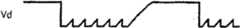
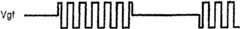
当将来自于这种调制部件100的输出信号施加到脉冲变压器6的初级线圈上时,在脉冲变压器6的次级线圈中,如图2E所示,感应出与载波信号Vc波形相似的电压Vgf。通过该电压Vgf,包含在解调部件200中的FET 7被交替地施加正电压和负电压以作为门信号,从而导通或截止。When an output signal from such a
当电压Vgf为正的时,因为FET 7导通,所以电容10中所充电的电荷进行放电。当电压Vgf为负的时,因为FET 7截止,所以电容10经电阻9利用来自于电源8的电荷进行充电。When the voltage Vgf is positive, the charge charged in the
在此,电容10的放电速度取决于电容10的容量和FET 7的导通电阻。另外电容10的充电速度取决于电容10和电阻9的时间常数。在通常情况下,将电阻9的阻值设定成大于FET 7的导通电阻的阻值。Here, the discharge speed of the
此外,如果FET7的截止持续,则电容10的电压Vd上升,但是在载波信号Vc的周期内每次施加使FET7变为导通的电压Vgf时,电容10的电荷都会被放电。因此,反相驱动器11的输入信号Vd不会变为高电平(参照图2)。换言之,在载波信号Vc的周期内,要不让FET 7导通/截止,就必须要将电容10和电阻9的时间常数设定得很长。Also, if the FET7 is kept off, the voltage Vd of the
然而,如果该时间常数过长的话,因为对于ON/OFF信号Vs的IGBT 12的栅极信号Vgi的时延变长,则必须将时间常数或载波信号Vc的周期设定成使这种时延不给IGBT 12的动作带来不良影响的程度。However, if the time constant is too long, since the time delay of the gate signal Vgi of the
当电容10的电荷被放电,反相驱动器11的输入信号Vd变为低电平后,反相驱动器11就使IGBT 12的栅极电压Vgi上升至电源8的电压电平附近,从而使IGBT 12导通(参照图2G)。When the charge of the
当从信号源1输出逻辑电平为低电平的ON/OFF信号后,则第一和第二与门4、5的输出信号Vp1、Vp2同时为零电平。因此,FET 7的栅极电压Vgf也变为零电平,FET7变为截止。在此,如果FET 7的截止持续,则电容10的电压上升,一旦超出反相驱动器11的输入电平的阈值,就从反相驱动器11输出用于使IGBT 12截止的栅极电压Vgi。When the
如上所述,包含在解调部件200中的反相驱动器11输出使输入数字信号(ON/OFF信号)Vs的波形恢复(解调)的栅极电压Vgi。由此,作为结果,IGBT 12进行对应于输入数字信号Vs的驱动控制。As described above, the inversion driver 11 included in the
根据本实施例,不使用光耦合器,而使用由脉冲变压器6构成的绝缘传送部件,从而能够实现数字信号传送电路即IGBT 12的门信号传送电路。脉冲变压器6与光耦合器相比,由于其在高温环境下的工作特性优良,因此能够实现可靠性高的数字信号传送电路。According to the present embodiment, the gate signal transmission circuit of the
此外,通过提高载波信号源2的输出频率,由于能够减低脉冲变压器6的磁通量,在能够使脉冲变压器6小型化的同时,能够提高ON/OFF信号Vs的传送速度。因此,可以实现能高速传送的数字信号传送电路。Furthermore, by increasing the output frequency of the
(变形例)(Modification)
进而,在第一和第二与门4、5的各个输出端上,即使连接有用于放大电压或电流的缓冲器电路,本实施例的技术效果也是相同的。Furthermore, even if a buffer circuit for amplifying voltage or current is connected to each output terminal of the first and second AND
此外,在硅衬底上形成高耐压绝缘膜,把脉冲变压器6的初级线圈和次级线圈之间进行绝缘,在该硅衬底上形成脉冲变压器6的线圈、初级侧的电路2~5以及次级线圈侧的电路7、9、10、11的一部分或全部,则可以将本实施例所涉及的数字信号传送电路集成电路化为单芯片的IC。由此,就能够实现小型且廉价的数字信号传送电路。In addition, a high withstand voltage insulating film is formed on a silicon substrate to insulate the primary coil of the
(第二实施例)(second embodiment)
图3和图4A~图4G是用来说明第二实施例所涉及的数字信号传送电路的图。下面,参照图3和图4A~图4G,说明第二实施例所涉及的数字信号传送电路的结构及技术效果。3 and 4A to 4G are diagrams for explaining a digital signal transmission circuit according to the second embodiment. Next, the configuration and technical effects of the digital signal transmission circuit according to the second embodiment will be described with reference to FIGS. 3 and 4A to 4G.
另外,在图3所示的本实施例中,对于同图1中所示的第一实施例相同的结构及动作,附上相同符号,并省略其详细说明。In addition, in the present embodiment shown in FIG. 3, the same structures and operations as those of the first embodiment shown in FIG. 1 are assigned the same reference numerals, and detailed description thereof will be omitted.
本实施例的调制部件100具有第一与非门电路(以下称为第一与非门)13和第二与非门电路(以下称为第二与非门)14。The
第一与非门13其第一输入端连接于信号源1的输出端,第二输入端连接于载波信号源2的输出端。并且,第一与非门13根据ON/OFF信号Vs输出对载波信号Vc进行了调制(门控制)的输出信号Vp3(参照图4C)。The first input end of the first NAND gate 13 is connected to the output end of the
另一方面,第二与非门14其第一输入端连接于信号源1的输出端,第二输入端连接于反相器3的输出端,根据ON/OFF信号Vs输出对载波信号Vc的反相信号进行了调制(门控制)的输出信号Vp4(参照图4D)。On the other hand, the first input end of the second NAND gate 14 is connected to the output end of the
也就是说,在本实施例中,调制就意味着利用第一和第二与非门13、14的与非逻辑运算(与非门控制)动作。That is to say, in this embodiment, modulation means the NAND logic operation (NAND gate control) action using the first and second NAND gates 13 and 14 .
脉冲变压器6其初级线圈连接于第一和第二与非门13、14各输出端。The primary coil of the
如图4A、图4B、图4C所示,如果从载波信号源2中输出高频载波信号Vc、又从信号源1输出高电平的ON/OFF信号Vs,则从第一与非门13中输出作为该各个信号Vs、Vc的与非运算结果的信号Vp3。另一方面,如图4D所示,从第二与非门14中输出第一与非门13的输出信号Vp3的反相信号Vp4。As shown in Figure 4A, Figure 4B, and Figure 4C, if the high-frequency carrier signal Vc is output from the
当将来自于这种调制部件100的输出信号施加到脉冲变压器6的初级线圈上后,在脉冲变压器6的次级线圈中,如图4E所示,就会感应出与载波信号Vc相似波形的电压Vgf。通过此电压Vgf,在包含于解调部件200中的FET 7中,交替地施加正电压和负电压以作为门信号,从而使FET 7导通或截止。When the output signal from the modulating
当从信号源1中输出低电平的ON/OFF信号Vs后,第一和第二与非门13、14的输出信号Vp3、Vp4就同时变为相同的电压电平。此时,FET 7的栅极电压Vgf变为零电平,FET 7变为截止状态(参照图4E)。When the low-level ON/OFF signal Vs is output from the
也就是说,本实施例的FET 7的栅极电压Vgf成为使前述第一实施例的栅极电压Vgf反相的波形。为此,同前述第一实施例的情况相比,反相驱动器11的门信号Vd成为相对于载波信号Vc相错最大半周期的波形。然而,相对于ON/OFF信号Vs的频率,当载波信号Vc的频率非常高时,该相错不会成为2。因此,本实施例的解调部件200为依照ON/OFF信号(数字信号)Vs,输出用于对IGBT 12进行导通截止控制的栅极电压Vgi(参照图4G)。That is, the gate voltage Vgf of the
如上所述的本实施例,由于从调制部件100输出的信号Vp3、Vp4以及感应电压Vgf相对于第一实施例的情况成为反相的波形,因此其结果是,能够获得同该第一实施例相同的技术效果。In this embodiment as described above, since the signals Vp3, Vp4 and the induced voltage Vgf output from the
(变形例)(Modification)
此外,在第一和第二与非门13、14的各输出端上,即使连接有用于放大电压或电流的缓冲器电路,本实施例的技术效果也是相同的。In addition, even if a buffer circuit for amplifying voltage or current is connected to each output terminal of the first and second NAND gates 13 and 14, the technical effect of this embodiment is the same.
(第三实施例)(third embodiment)
图5和图6A~图6G是用来说明第三实施例所涉及的数字信号传送电路的图。下面,参照图5和图6A~图6G,说明第三实施例所涉及的数字信号传送电路的结构及技术效果。5 and 6A to 6G are diagrams for explaining a digital signal transmission circuit according to the third embodiment. Next, the configuration and technical effects of the digital signal transmission circuit according to the third embodiment will be described with reference to FIG. 5 and FIGS. 6A to 6G.
另外,在图5所示的本实施例中,对于与图1中所示的第一实施例相同的结构及动作,附上相同的符号,并省略其详细说明。In addition, in the present embodiment shown in FIG. 5, the same structures and operations as those of the first embodiment shown in FIG. 1 are assigned the same reference numerals, and detailed description thereof will be omitted.
本实施例的调制部件100具有第一或门电路(以下称为第一或门)15和第二或门电路(以下称为第二或门)16。此外,本实施例的解调部件200具有输出IGBT 12的栅极信号Vgi的非反相驱动器17。The
第一或门15其第一输入端连接于信号源1的输出端,第二输入端连接于载波信号源2的输出端。并且,第一或门15根据ON/OFF信号Vs输出将载波信号Vc进行了调制(门控制)的输出信号Vp5(参照图6C)。The first input end of the first OR
另一方面,第二或门16其第一输入端连接于信号源1的输出端,第二输入端连接于反相器3的输出端,根据ON/OFF信号Vs输出将载波信号Vc的反相信号进行了调制(门控制)的输出信号Vp6(参照图6D)。On the other hand, the first input end of the second OR
也就是说,在本实施例中,调制意味着利用第一和第二或门15、16的或逻辑运算(或门控制)动作。That is to say, in this embodiment, modulation means an OR logic operation (OR gate control) action using the first and second OR
脉冲变压器6其初级线圈连接于第一和第二或门15、16的各输出端。The primary coil of the
在解调部件200中,非反相驱动器17其输入端连接于电容10,输出端连接于IGBT 12的栅极端子。当对应于电容10的输入电压Vd为低电平时,非反相驱动器17向IGBT 12的栅极端子施加低电平的栅极信号Vgi。此外,当输入电压Vd变为高电平后,非反相驱动器17就将IGBT 12的栅极电压Vgi上升至电源8的电压电平附近,从而使IGBT 12导通(参照图6F、图6G)。In the
如图6C、图6D、图6E所示,根据来自于信号源1的ON/OFF信号Vs和来自于载波信号源2的载波信号Vc,当来自于调制部件100的输出信号Vp5、Vp6被施加到脉冲变压器6的初级线圈上后,则在脉冲变压器6的次级线圈中,就会感应出与载波信号Vc波形相似的电压Vgf。As shown in FIG. 6C, FIG. 6D, and FIG. 6E, according to the ON/OFF signal Vs from the
通过此电压Vgf,在包含于解调部件200中的FET 7中,交替地施加正电压和负电压以作为门信号,从而导通或截止。当来自于调制部件100的输出信号Vp5、Vp6同时为相同的电压电平时,FET 7的栅极电压Vgf变为零电平,从而使FET 7变为截止状态(参照图6E)。By this voltage Vgf, in the
当ON/OFF信号Vs为高电平时,非反相驱动器17的输入电压Vd成为高电平,Vs和Vd成为同相。为此,尽管非反相驱动器17相对于ON/OFF信号Vs产生微小时延,但输出与该信号Vs波形相似的栅极电压Vgi(参照图6G)。据此,依照ON/OFF信号(数字信号)Vs对IGBT 12进行导通截止控制。When the ON/OFF signal Vs is at a high level, the input voltage Vd of the
(变形例)(Modification)
在如上所述的本实施例的情况下,能够获得与第一实施例相同的技术效果。此外,在第一和第二或门15、16的各输出端上,即使连接有用于放大电压或电流的缓冲器电路,本实施例的技术效果也是相同的。In the case of the present embodiment as described above, the same technical effects as those of the first embodiment can be obtained. In addition, even if a buffer circuit for amplifying voltage or current is connected to each output terminal of the first and second OR
(第四实施例)(fourth embodiment)
图7和图8A~图8G是用来说明根据第四实施例的数字信号传送电路的图。下面,参照图7和图8A~图8G,说明第四实施例所涉及的数字信号传送电路的结构及技术效果。7 and 8A to 8G are diagrams for explaining a digital signal transmission circuit according to the fourth embodiment. Next, the configuration and technical effects of the digital signal transmission circuit according to the fourth embodiment will be described with reference to FIG. 7 and FIGS. 8A to 8G .
另外,在图7所示的本实施例中,对于同图1中所示的第一实施例及图5中所示的第三实施例相同的结构和动作,附上相同的符号,并省略其详细说明。In addition, in the present embodiment shown in FIG. 7 , for the same structures and actions as those of the first embodiment shown in FIG. 1 and the third embodiment shown in FIG. 5 , the same symbols are attached and omitted. its detailed description.
本实施例的调制部件100具有第一或非门电路(以下称为第一或非门)18和第二或非门电路(以下称为第二或非门)19。第一或非门18其第一输入端连接于信号源1的输出端,第二输入端连接于载波信号源2的输出端。第一或非门18根据ON/OFF信号Vs输出将载波信号Vc进行了调制(门控制)的输出信号Vp7(参照图8)。The
另一方面,在第二或非门19中其第一输入端连接于信号源1的输出端,第二输入端连接于反相器3的输出端。第二或非门19根据ON/OFF信号Vs输出对载波信号Vc的反相信号进行了调制(门控制)的输出信号Vp8(参照图8D)。On the other hand, the first input terminal of the second NOR gate 19 is connected to the output terminal of the
也就是说,在本实施例中,调制意味着利用第一和第二或非门18、19的或非逻辑运算(或非门控制)动作。That is to say, in this embodiment, modulation means the NOR logic operation (NOR gate control) action using the first and second NOR gates 18 , 19 .
脉冲变压器6其初级线圈连接于第一和第二或非门18、19的各输出端。The primary winding of the
在本实施例中,如图8所示,尽管自调制部件100输出的信号Vp7、Vp8以及感应电压Vgf相对于前述第三实施例的情况成为反相的波形,但作为结果能够获得与该第三实施例相同的技术效果。In the present embodiment, as shown in FIG. 8, although the signals Vp7, Vp8 and the induced voltage Vgf output from the
(变形例)(Modification)
此外,在第一和第二或非门18、19的各输出端上,即使连接有用于放大电压或电流的缓冲器电路,本实施例的技术效果也是相同的。In addition, even if a buffer circuit for amplifying voltage or current is connected to each output terminal of the first and second NOR gates 18, 19, the technical effect of this embodiment is the same.
(第五实施例)(fifth embodiment)
图9和图10A~图10F是用来说明第五实施例所涉及的数字信号传送电路的图。下面,参照图9和图10A~图10F,说明第五实施例所涉及的数字信号传送电路的结构及技术效果。9 and 10A to 10F are diagrams for explaining a digital signal transmission circuit according to the fifth embodiment. Next, the configuration and technical effects of the digital signal transmission circuit according to the fifth embodiment will be described with reference to FIGS. 9 and 10A to 10F.
另外,在图9所示的本实施例中,对于同图1中所示的第一实施例相同的结构和动作,附上相同的符号,并省略其详细说明。In addition, in the present embodiment shown in FIG. 9, the same structures and operations as those of the first embodiment shown in FIG. 1 are assigned the same reference numerals, and detailed description thereof will be omitted.
本实施例的调制部件100具有异或门电路(以下称为异或门)20和缓冲器电路21。The
异或门20其第一输入端连接于信号源1的输出端,第二输入端连接于载波信号源2的输出端。异或门20根据ON/OFF信号Vs输出对载波信号Vc进行了调制(门控制)的输出信号Vp9(参照图10C)。The first input end of the XOR gate 20 is connected to the output end of the
也就是说,在本实施例中,调制意味着利用异或门20的异或逻辑运算(异或门控制)操作。That is, in the present embodiment, modulation means an exclusive OR logic operation (exclusive OR gate control) operation using the exclusive OR gate 20 .
另一方面,缓冲器电路21其第一输入端连接于载波信号源2的输出端,第二输入端接地,并连接于反相器3的输出端。缓冲器电路21是与载波信号Vc相似的波形,输出与异或门20的输出相同振幅的电压。On the other hand, the first input terminal of the buffer circuit 21 is connected to the output terminal of the
在此,异或门20由于需要运算时间,因而相对于输入信号,输出信号的应答反应被时延数纳秒。缓冲器电路21把确保与此同等的时延作为目的,为了向脉冲变压器6施加与载波信号Vc波形相似的(时间比率相等的)波形是有效的。但是,如果相对于载波信号Vc的频率异或门20的运算时间为充分短的时间、或者通过改变载波信号Vc的时间比率和施加于脉冲变压器6的电压的时间比率而导致脉冲变压器6不饱和,则就不一定需要缓冲器电路21。Here, since the exclusive OR gate 20 requires operation time, the response response of the output signal is delayed by several nanoseconds relative to the input signal. The buffer circuit 21 aims at securing a time delay equivalent to this, and it is effective to apply a waveform similar to the waveform of the carrier signal Vc (with the same time ratio) to the
在如上所述的这个实施例的情况下,也能够获得与第一实施例相同的技术效果。此外,同第一到第四实施例相比,由于可以不要反相器3,因而能够简化电路结构。再有,由于如上所述的理由,假如还省略掉缓冲器电路21的话,则就能更加简化电路结构。Also in the case of this embodiment as described above, the same technical effect as that of the first embodiment can be obtained. Furthermore, since the
(第六实施例)(sixth embodiment)
图11和图12A~图12G是用来说明第六实施例所涉及的数字信号传送电路的图。下面,参照图11和图12A~图12G,说明第六实施例所涉及的数字信号传送电路的结构及技术效果。11 and 12A to 12G are diagrams for explaining a digital signal transmission circuit according to the sixth embodiment. Next, the configuration and technical effects of the digital signal transmission circuit according to the sixth embodiment will be described with reference to FIG. 11 and FIGS. 12A to 12G.
本实施例所涉及的数字信号传送电路具有高频信号源22、缓冲器电路23、反相器24、脉冲变压器26、输入用开关电路27、延迟电路28和闩锁电路29。The digital signal transmission circuit according to this embodiment has a high
高频信号源22在脉冲变压器26为不饱和程度下输出高频的矩形波信号。缓冲器电路23连接于高频信号源22的输出端,并输出与从该高频信号源22输出的矩形波信号波形相似的波形的信号Vp10(参照图12B)。The high-
在另一方面,反相器24连接于高频信号源22的输出端,并输出从该高频信号源22输出的将矩形波信号反相的信号(相位相差180°)的信号Vp11(参照图12C)。因此,缓冲器电路23的输出信号Vp10和反相器24的输出信号Vp11成为相互反相的信号。在此,缓冲器电路23及反相器24都是提供为了驱动脉冲变压器26所需的电压和电流的组成部分。On the other hand, the
脉冲变压器26在其初级线圈的一端上经电阻25连接于反相器24的输出端,在另一端上连接于缓冲器电路23的输出端。在脉冲变压器26的次级线圈上,连接开关电路27。开关电路27通过打开和闭合动作(相当于逻辑电平的高电平和低电平),来控制脉冲变压器26的次级线圈短路和开路。The
延迟电路28连接于高频信号源22的输出端,输出比从高频信号源22输出的矩形波信号仅延迟延迟时间Td的闩锁信号VI(参照图12F)。The
闩锁电路29连接于电阻25,在从延迟电路28输出的闩锁信号VI的上升沿定时,输出对在电阻25的一端上产生的电压信号Vsens进行闩锁所了的信号Vout(参照图12G)。换言之,闩锁电路29相当于恢复与开关电路27的导通截止动作相应的数字输入的解调电路。The
接下来,对本实施例的动作进行说明。Next, the operation of this embodiment will be described.
如图12A所示,开关电路27相当于前述的ON/OFF信号Vs,意味着高电平为闭合状态,低电平为打开状态。即,当开关电路27为闭合状态时,脉冲变压器26的次级线圈就被短路。这样一来,因为使电阻25的电阻值比该脉冲变压器26的线圈阻抗更大,所以可以将脉冲变压器26的初级线圈的电压看作为零电平。As shown in FIG. 12A , the
因此,闩锁电路29的输入信号Vsens成为与缓冲器电路23的输出信号(电压)Vp10相等(参照图12E)。闩锁电路29在延迟时间Td的某个闩锁信号VI的上升沿的定时闩锁输入信号Vsens,并输出输出电压Vout(参照图12G)。Therefore, the input signal Vsens of the
在此,输出电压Vout虽然因延迟时间Td而不同,但是当该延迟时间Td比高频信号源22所输出的矩形波信号的半个周期还要短时,它就变为高电平。另外,当该延迟时间Td比半个周期长且比一个周期短时,输出电压Vout变为低电平。在本实施例中,将该延迟时间Td设定为比高频信号源22所输出的矩形波信号的半个周期还要短,如图12A、图12G所示,当开关电路27为闭合状态时,闩锁电路29的输出信号Vout变为高电平。Here, although the output voltage Vout differs depending on the delay time Td, when the delay time Td is shorter than half a cycle of the rectangular wave signal output from the high-
当开关电路27变为打开状态时,脉冲变压器26的次级线圈被开路。此时,在电阻25与脉冲变压器26的励磁阻抗上施加“Vp10-Vp11”的矩形波电压,流过电阻25的电流Ir变为流过的锯齿状波形(参照图12D)。When the
在通过流过这个电流Ir而导致电阻R25的电压下降部分上,施加了反相器24的输出电压Vp11的电压就变为闩锁电路29的输入电压Vsens。这个输入电压Vsens在Vp10为低电平时比为高电平时还要高,从而开关电路27转换成闭合状态。因此,如图12A、图12G所示,当开关电路27为打开状态时,闩锁电路29的输出信号Vout变为低电平。The voltage at which the output voltage Vp11 of the
在此,当开关电路27为打开状态时,如图12E所示,闩锁电路29的输入信号Vsens处于尖锐形状。在这种情况下,如果逐渐加大脉冲变压器26的励磁阻抗的话,则就逐渐接近于反相器24的输出信号Vp11的波形。即,在开关电路27为打开状态和闭合状态下时,闩锁电路29的输入信号Vsens变为电压波形反相的波形。Here, when the
总之根据上面所述的本实施例,使用脉冲变压器26,在开关电路27是绝缘的状态下,就可以构成把开关电路27的开闭状态作为电压信号来取得这样的开关开闭监视电路。换言之,使用同光耦合器相比在高温环境下工作特性优良的脉冲变压器26,就可以实现根据开关电路27的开闭来传送数字信号的可靠性高的数字信号传送电路。In short, according to the present embodiment described above, the
特别是,根据本实施例的结构,在开关电路27一侧上没有必要有电源,由于可以将开关电路27以外的电路集中在脉冲变压器26的初级一侧上,因而能够实现整个电路的简化。In particular, according to the structure of this embodiment, there is no need for a power supply on the switching
此外,通过提高高频信号源22的输出频率,由于能够减少脉冲变压器26的磁通量,同时能够使脉冲变压器26小型化,因此能够提高开关电路27的开闭状态的传送速度。In addition, by increasing the output frequency of the high-
(第七实施例)(seventh embodiment)
图13是用来说明第七实施例所涉及的数字信号传送电路的图。下面,参照图13,说明第七实施例所涉及的数字信号传送电路的结构及技术效果。FIG. 13 is a diagram for explaining a digital signal transmission circuit according to the seventh embodiment. Next, referring to FIG. 13, the configuration and technical effect of the digital signal transmission circuit according to the seventh embodiment will be described.
另外,在图13所示的本实施例中,对于与图11所示的第六实施例相同的结构和动作,附上相同的符号,并省略其详细说明。In addition, in the present embodiment shown in FIG. 13, the same reference numerals are attached to the same configurations and operations as those of the sixth embodiment shown in FIG. 11, and detailed description thereof will be omitted.
在本实施例中,如图13所示,脉冲变压器26的次级线圈连接于整流器30的交流端子。整流器30其直流端子连接于FET 31的漏极端子和源极端子。In this embodiment, the secondary coil of the
输入信号源32产生高电平和低电平的二值数字信号。FET 31其栅极连接于输入信号源32的输出端,依照从输入信号源32产生的数字信号导通或截止。The
接下来,说明本实施例的动作。Next, the operation of this embodiment will be described.
如果从输入信号源32输出的数字信号变为高电平,则FET 31就变为导通状态。据此,脉冲变压器26的次级线圈经整流器30变成短路状态。因此,正如在上述第六实施例中说明的那样,如果脉冲变压器26的次级线圈为短路,则闩锁电路29的输出信号Vout就变为高电平(参照与图12A的关闭状态相同的图G)。If the digital signal output from the
此外,如果从输入信号源32输出的数字信号变为低电平,则FET 31就变为截止状态。据此,脉冲变压器26的次级线圈变成开路状态。因此,闩锁电路29的输出信号Vout变为低电平(参照与图12A的导通状态相同的图G)。Also, if the digital signal output from the
总之根据上面所述的本实施例,通过依照从输入信号源32输出的数字信号的逻辑电平,闩锁电路29的输出信号Vout发生变化,作为结果,就能够绝缘传送数字信号。In short, according to the present embodiment described above, the output signal Vout of the
在此,假设如下这样的情况,即:FET 31导通时整流器30上所产生的电压降同FET 31截止时脉冲变压器26的次级线圈上所感应的电压的振幅相比是不可忽视的大小的情况。在这种情况下,在闩锁电路29的输入电压Vsens上产生的FET 31的导通时与截止时之差变小,从而使因噪声而引起误动作的可能性增高。Here, it is assumed that the voltage drop generated across the
然而,为了使FET 31导通时整流器30上所产生的电压降同FET 31截止时脉冲变压器26的次级线圈上所感应的电压的振幅相比变得足够小,通过将缓冲器电路23和反相器24的输出电压规格参数设高、将脉冲变压器26的次级线圈的匝数比设高等等,就可以对上述这样的误动作的发生防患于未然。However, in order to make the voltage drop generated on the
根据如上所述的这个实施例,与上述第六实施例相同,使用了同光耦合器相比在高温环境下工作特性优良的脉冲变压器26,从而能够实现可靠性高的数字信号传送电路。According to this embodiment as described above, as in the sixth embodiment described above, the
此外,如果在硅上形成高耐压的绝缘膜,使脉冲变压器26的初级线圈和次级线圈之间绝缘,并在硅上形成脉冲变压器26的线圈、初级端和次级端的各个电路22~31的一部分或全部,那么由于可将该电路集成化为单芯片IC,因而就可以实现小型而廉价的数字信号传送电路。In addition, if a high withstand voltage insulating film is formed on silicon, the primary coil and secondary coil of the
(第八实施例)(eighth embodiment)
图14是用来说明第八实施例所涉及的数字信号传送电路的图。下面,参照图14,说明第八实施例所涉及的数字信号传送电路的结构及技术效果。FIG. 14 is a diagram for explaining a digital signal transmission circuit according to the eighth embodiment. Next, referring to FIG. 14, the configuration and technical effect of the digital signal transmission circuit according to the eighth embodiment will be described.
另外,在图14所示的本实施例中,对于与图11所示的第六实施例相同的结构和动作,附上相同的符号,并省略其详细说明。In addition, in the present embodiment shown in FIG. 14, the same reference numerals are assigned to the same configurations and operations as those of the sixth embodiment shown in FIG. 11, and detailed description thereof will be omitted.
在本实施例中,如图14所示,脉冲变压器26的次级线圈的两端分别连接FET 33和FET 34的各漏极端子。FET 33和FET 34的各源极端子相互连接。FET 33和FET 34其各栅极端子连接于输入信号源32的输出端,并依照从输入信号源32产生的数字信号而导通或截止。In this embodiment, as shown in FIG. 14 , both ends of the secondary coil of the
接下来,说明本实施例的动作。Next, the operation of this embodiment will be described.
如果从输入信号源32输出的数字信号成为高电平,则FET 33和FET 34就变为导通状态。据此,脉冲变压器26的次级线圈变成短路状态。因此,正如在上述第六实施例中所述的那样,如果脉冲变压器26的次级线圈短路后,则闩锁电路29的输出信号Vout就变为高电平(参照与图12A的闭合状态相同的图G)。If the digital signal output from the
此外,如果从输入信号源32输出的数字信号成为低电平,则FET 33和FET34就变为截止状态。据此,脉冲变压器26的次级线圈变成开路状态。因此,闩锁电路29的输出信号Vout就变为低电平(参照与图12A的打开状态相同的图G)。Also, if the digital signal output from the
总之根据上面所述的这个实施例,与上述第七实施例相同,通过依照从输入信号源32输出的数字信号的逻辑电平,闩锁电路29的输入信号Vout发生变化,作为结果,能够绝缘传送数字信号。In short, according to this embodiment described above, as in the seventh embodiment described above, by changing the input signal Vout of the
再有,本实施例由于是在脉冲变压器26的次级线圈短路时未使用整流器的结构,因此同上述第七实施例相比,能够实现误动作的可能性小的数字信号传送电路。In addition, since the present embodiment does not use a rectifier when the secondary coil of the
(第九实施例)(ninth embodiment)
图15是用来说明第九实施例所涉及的数字信号传送电路的图。FIG. 15 is a diagram for explaining a digital signal transmission circuit according to the ninth embodiment.
下面,参照图15,说明第九实施例所涉及的数字信号传送电路的结构及技术效果。Next, referring to FIG. 15, the configuration and technical effects of the digital signal transmission circuit according to the ninth embodiment will be described.
另外,在图15所示的这个实施例中,对于与图14所示的第八实施例相同的结构和动作,附上相同的符号,并省略其详细说明。In this embodiment shown in FIG. 15, the same structures and operations as those of the eighth embodiment shown in FIG. 14 are denoted by the same reference numerals, and detailed description thereof will be omitted.
在本实施例中,如图15所示,在设在脉冲变压器26的初级一侧的电阻25的两端连接有第一电容35。此外,在脉冲变压器26和电阻25的连接点与脉冲变压器26的初级线圈一侧的接地点之间连接有第二电容36。利用这些电阻25、第一和第二电容35、36,发挥用于消除以下这种高频电流中所带有的某种噪声的滤波装置的功能。In this embodiment, as shown in FIG. 15 , a first capacitor 35 is connected to both ends of the
接下来,说明本实施例的动作。Next, the operation of this embodiment will be described.
由于在脉冲变压器26的初级线圈和次级线圈之间存在寄生电容,因而当发生初级线圈和次级线圈的电位变化等情况,噪声就会通过寄生电容而流入到初级线圈一侧中。由此,闩锁电路29的输入电压Vsens的波形就会失掉原形,从而就会有闩锁电路29错误地输出输出信号Vout的情况发生。Since there is a parasitic capacitance between the primary coil and the secondary coil of the
使用第二电容36,使流入脉冲变压器26的初级端上的噪声流入到接地面、防止闩锁电路29误动作。但是,如果增大第二电容36的电容量,则由于闩锁电路29的输入信号Vsens的高频分量被消除,因而闩锁电路29得不到足够的输入电平,从而就会有无法正常进行数字信号传送的情况发生。Using the second capacitor 36, the noise flowing into the primary side of the
因此,第一电容35降低了反相器24和脉冲变压器26之间的高频阻抗,用它来确保闩锁电路29的输入电平。此外,第一电容35既起到降低对于噪声分量的阻抗的作用,又有避免因上述噪声而引起的误动作的效果。Therefore, the first capacitor 35 lowers the high-frequency impedance between the
根据上面所述的这个实施例,使用同光耦合器相比在高温环境下工作特性优良的脉冲变压器26,就能够实现可靠性高且因噪声而引起误动作的可能性小的数字信号传送电路。According to the above-described embodiment, a digital signal transmission circuit with high reliability and low possibility of malfunction due to noise can be realized by using the
另外,本发明并仅不限于上述实施例,而是在实施阶段能够在不脱离本发明范围的情况下改变结构组成部分,并加以具体化。另外,通过对上述实施例中所公开的多个结构组成部分的适当组合,可以形成多种发明。例如,也可以从实施例中所示的所有结构组成部分去掉某几个结构组成部分。而且,适当组合涉及不同实施例的结构组成部分也是可以的。In addition, the present invention is not limited to the above-mentioned embodiments, but structural components can be changed and embodied at the stage of implementation without departing from the scope of the present invention. In addition, various inventions can be formed by appropriately combining a plurality of structural components disclosed in the above embodiments. For example, it is also possible to remove certain structural constituents from all structural constituents shown in the embodiments. Also, it is possible to appropriately combine structural components related to different embodiments.
Claims (9)
Translated fromChineseApplications Claiming Priority (3)
| Application Number | Priority Date | Filing Date | Title |
|---|---|---|---|
| JP2004254453 | 2004-09-01 | ||
| JP2004254453AJP2006074372A (en) | 2004-09-01 | 2004-09-01 | Digital signal transmission device |
| JP2004-254453 | 2004-09-01 |
Publications (2)
| Publication Number | Publication Date |
|---|---|
| CN1750526A CN1750526A (en) | 2006-03-22 |
| CN1750526Btrue CN1750526B (en) | 2010-06-23 |
Family
ID=35463962
Family Applications (1)
| Application Number | Title | Priority Date | Filing Date |
|---|---|---|---|
| CN200510113293.5AExpired - Fee RelatedCN1750526B (en) | 2004-09-01 | 2005-09-01 | Digital signal transfer device |
Country Status (4)
| Country | Link |
|---|---|
| US (1) | US7671372B2 (en) |
| EP (1) | EP1633046A3 (en) |
| JP (1) | JP2006074372A (en) |
| CN (1) | CN1750526B (en) |
Families Citing this family (15)
| Publication number | Priority date | Publication date | Assignee | Title |
|---|---|---|---|---|
| JP2007305702A (en)* | 2006-05-10 | 2007-11-22 | Toshiba Corp | Semiconductor device and manufacturing method thereof |
| US8345779B2 (en)* | 2008-04-01 | 2013-01-01 | Microsemi Corporation | Pulse transformer driver |
| US8164157B2 (en)* | 2008-07-27 | 2012-04-24 | David Robert Morgan | Signal absorption induction circuit |
| JP4640495B2 (en)* | 2008-11-27 | 2011-03-02 | トヨタ自動車株式会社 | Electrically isolated switching element drive device |
| JP5462880B2 (en)* | 2009-08-10 | 2014-04-02 | 株式会社 日立パワーデバイス | Power converter |
| CN101854158A (en)* | 2010-05-28 | 2010-10-06 | 上海集成电路研发中心有限公司 | D-type flip-flop unit and frequency divider with the same |
| DE102010038735B3 (en) | 2010-07-30 | 2011-11-17 | Semikron Elektronik Gmbh & Co. Kg | Method for operating a PWM output of a driver for a power semiconductor |
| US10270630B2 (en) | 2014-09-15 | 2019-04-23 | Analog Devices, Inc. | Demodulation of on-off-key modulated signals in signal isolator systems |
| US9660848B2 (en) | 2014-09-15 | 2017-05-23 | Analog Devices Global | Methods and structures to generate on/off keyed carrier signals for signal isolators |
| US10536309B2 (en) | 2014-09-15 | 2020-01-14 | Analog Devices, Inc. | Demodulation of on-off-key modulated signals in signal isolator systems |
| US9998301B2 (en) | 2014-11-03 | 2018-06-12 | Analog Devices, Inc. | Signal isolator system with protection for common mode transients |
| CN105429435B (en)* | 2015-11-11 | 2018-09-11 | 广州金升阳科技有限公司 | The isolation transmission method of signal and the isolation and transmission circuit of signal |
| JP6685192B2 (en)* | 2016-07-11 | 2020-04-22 | 三菱電機株式会社 | Signal transmission device and power switching element drive device |
| CN108649936B (en)* | 2018-07-25 | 2021-11-23 | 合肥工业大学 | Magnetic isolation driven pulse width modulation and demodulation circuit |
| DE102018132936A1 (en)* | 2018-12-19 | 2020-06-25 | Endress+Hauser SE+Co. KG | Transmitter for transmitting digital signals between galvanically isolated circuit parts and field device with such a transmitter |
Citations (2)
| Publication number | Priority date | Publication date | Assignee | Title |
|---|---|---|---|---|
| CN1258406A (en)* | 1997-03-31 | 2000-06-28 | 株式会社日立制作所 | Modem using capacitive insulating barrier, insulating coupler, and integrated circuit used in modem |
| CN1267159A (en)* | 1999-08-24 | 2000-09-20 | 南宁胜利科技股份有限公司 | Wireless modem based on wireless data transmission network |
Family Cites Families (10)
| Publication number | Priority date | Publication date | Assignee | Title |
|---|---|---|---|---|
| GB2102230A (en)* | 1981-07-16 | 1983-01-26 | Plessey Co Ltd | A pulse drive circuit |
| US4644321A (en)* | 1984-10-22 | 1987-02-17 | Westinghouse Electric Corp. | Wireless power line communication apparatus |
| US5399913A (en)* | 1992-09-02 | 1995-03-21 | Exide Elecronics Corp. | Gate-drive circuit |
| DE29617892U1 (en)* | 1996-10-15 | 1996-11-28 | Schuster, Wolfgang, Dipl.-Ing., 88410 Bad Wurzach | Isolating control circuit for an electronic switch |
| US5781040A (en)* | 1996-10-31 | 1998-07-14 | Hewlett-Packard Company | Transformer isolated driver for power transistor using frequency switching as the control signal |
| KR19990072936A (en)* | 1998-02-27 | 1999-09-27 | 가나이 쓰도무 | Isolator and modem unit using the same |
| US6658051B1 (en)* | 2000-10-31 | 2003-12-02 | Centillium Communications, Inc. | Electrical isolation techniques for DSL modem |
| US7277491B2 (en)* | 2002-05-14 | 2007-10-02 | Ess Technology, Inc. | Data access arrangement using a high frequency transformer for electrical isolation |
| DE10312704A1 (en)* | 2003-03-21 | 2004-09-30 | Conti Temic Microelectronic Gmbh | Method for controlling and monitoring the function of a power semiconductor switch and device for carrying out the method |
| CN1830199A (en)* | 2003-05-29 | 2006-09-06 | Tdk半导体公司 | Method and apparatus for full-duplex signal across transformer |
- 2004
- 2004-09-01JPJP2004254453Apatent/JP2006074372A/enactivePending
- 2005
- 2005-08-31EPEP05018896Apatent/EP1633046A3/ennot_activeWithdrawn
- 2005-08-31USUS11/215,126patent/US7671372B2/ennot_activeExpired - Fee Related
- 2005-09-01CNCN200510113293.5Apatent/CN1750526B/ennot_activeExpired - Fee Related
Patent Citations (2)
| Publication number | Priority date | Publication date | Assignee | Title |
|---|---|---|---|---|
| CN1258406A (en)* | 1997-03-31 | 2000-06-28 | 株式会社日立制作所 | Modem using capacitive insulating barrier, insulating coupler, and integrated circuit used in modem |
| CN1267159A (en)* | 1999-08-24 | 2000-09-20 | 南宁胜利科技股份有限公司 | Wireless modem based on wireless data transmission network |
Also Published As
| Publication number | Publication date |
|---|---|
| US7671372B2 (en) | 2010-03-02 |
| JP2006074372A (en) | 2006-03-16 |
| CN1750526A (en) | 2006-03-22 |
| EP1633046A2 (en) | 2006-03-08 |
| EP1633046A3 (en) | 2009-10-21 |
| US20060043389A1 (en) | 2006-03-02 |
Similar Documents
| Publication | Publication Date | Title |
|---|---|---|
| CN1750526B (en) | Digital signal transfer device | |
| US8643407B2 (en) | High temperature half bridge gate driver | |
| CN107612532B (en) | Signal transmission device and power switching element drive device | |
| US8928363B2 (en) | Semiconductor drive circuit and power conversion apparatus using same | |
| US10171130B2 (en) | Receiver circuit | |
| JP2018102119A (en) | Insulation type dc/dc converter | |
| CN101677240B (en) | Isolated gate bipolar transistor driving circuit | |
| JP5861054B2 (en) | High frequency receiver circuit and insulated signal transmission device | |
| KR20080074875A (en) | Circuit device and method for galvanic isolation control of semiconductor switch | |
| CN109690931B (en) | Power conversion device, control device for power conversion device, and control method for power conversion device | |
| CN117203884A (en) | Driving device for semiconductor switching element, driving method thereof and power conversion device | |
| JP2005020392A (en) | Signal transmission circuit and drive device | |
| EP4383571A1 (en) | Receiver circuit, corresponding isolated driver device, electronic system and method of decoding a differential signal into a digital output signal | |
| US7095184B2 (en) | Electronic ballast for a lamp to be operated using iterative voltage pulses | |
| WO2008101548A1 (en) | Level shift circuit | |
| JP2003299344A (en) | Gate drive circuit | |
| US7719861B2 (en) | Signal differentiation with differential conversion circuit | |
| US12407345B2 (en) | Switched inductive storage element to enhance gate drive at turn-off | |
| KR101970870B1 (en) | Gate voltage control device | |
| CN118157698A (en) | Receiver circuit, corresponding isolated driver device, electronic system and method for decoding differential signal into digital output signal | |
| JP2025125520A (en) | Isolation device having inductive and capacitive isolation circuits | |
| JPH04309010A (en) | Square wave generating circuit | |
| JP2002374667A (en) | Insulated drive circuit |
Legal Events
| Date | Code | Title | Description |
|---|---|---|---|
| C06 | Publication | ||
| PB01 | Publication | ||
| C10 | Entry into substantive examination | ||
| SE01 | Entry into force of request for substantive examination | ||
| C14 | Grant of patent or utility model | ||
| GR01 | Patent grant | ||
| C17 | Cessation of patent right | ||
| CF01 | Termination of patent right due to non-payment of annual fee | Granted publication date:20100623 Termination date:20110901 |