CN1744021A - Touch screen and manufacturing method thereof - Google Patents
Touch screen and manufacturing method thereofDownload PDFInfo
- Publication number
- CN1744021A CN1744021ACNA2005100958308ACN200510095830ACN1744021ACN 1744021 ACN1744021 ACN 1744021ACN A2005100958308 ACNA2005100958308 ACN A2005100958308ACN 200510095830 ACN200510095830 ACN 200510095830ACN 1744021 ACN1744021 ACN 1744021A
- Authority
- CN
- China
- Prior art keywords
- spacer
- touch screen
- spacers
- film
- conductive layer
- Prior art date
- Legal status (The legal status is an assumption and is not a legal conclusion. Google has not performed a legal analysis and makes no representation as to the accuracy of the status listed.)
- Granted
Links
Images


Classifications
- G—PHYSICS
- G06—COMPUTING OR CALCULATING; COUNTING
- G06F—ELECTRIC DIGITAL DATA PROCESSING
- G06F3/00—Input arrangements for transferring data to be processed into a form capable of being handled by the computer; Output arrangements for transferring data from processing unit to output unit, e.g. interface arrangements
- G06F3/01—Input arrangements or combined input and output arrangements for interaction between user and computer
- G06F3/03—Arrangements for converting the position or the displacement of a member into a coded form
- G06F3/041—Digitisers, e.g. for touch screens or touch pads, characterised by the transducing means
- G06F3/045—Digitisers, e.g. for touch screens or touch pads, characterised by the transducing means using resistive elements, e.g. a single continuous surface or two parallel surfaces put in contact
Landscapes
- Engineering & Computer Science (AREA)
- General Engineering & Computer Science (AREA)
- Theoretical Computer Science (AREA)
- Human Computer Interaction (AREA)
- Physics & Mathematics (AREA)
- General Physics & Mathematics (AREA)
- Position Input By Displaying (AREA)
- Push-Button Switches (AREA)
- Manufacture Of Switches (AREA)
Abstract
Translated fromChinese
Description
Translated fromChinese技术领域technical field
本发明涉及主要用于各种电子设备的触摸屏及其制造方法。The present invention relates to a touch screen mainly used in various electronic devices and a manufacturing method thereof.
背景技术Background technique
近年来,在移动电话或汽车导向系统等各种电子设备中,经常使用在液晶等显示元件的前面装有透光性触摸屏的设备。通过触摸屏对在背面的显示元件上显示出的文字或符号进行识别和选择,用手指或专用的笔等对触摸屏进行按压操作,从而进行设备各种功能的切换。对于这样的触摸屏,要求制造容易并且价格低廉。In recent years, in various electronic devices such as mobile phones and car navigation systems, devices in which a light-transmitting touch panel is mounted on the front of a display element such as a liquid crystal are often used. Identify and select the text or symbols displayed on the display element on the back through the touch screen, and press the touch screen with a finger or a special pen to switch various functions of the device. Such a touch panel is required to be easy to manufacture and inexpensive.
使用图5和图6来说明现有的触摸屏。A conventional touch panel will be described using FIG. 5 and FIG. 6 .
为了容易分辨其构成,图5、图6的截面图放大厚度方向上的尺寸表示。In order to easily distinguish its structure, the cross-sectional views of Fig. 5 and Fig. 6 are shown with enlarged dimensions in the thickness direction.
图5是现有的触摸屏的截面图。图5中在透光性的下基板51上面形成有氧化铟锡等透光性下导电层53,在薄膜状的透光性上基板52的下面同样形成有上导电层54。FIG. 5 is a cross-sectional view of a conventional touch screen. In FIG. 5 , a translucent lower
然后,在下导电层53的上面,以规定的间隔形成有多个由绝缘树脂形成的点间隔件(未图示)。在上导电层54的两端形成有一对上电极(未图示),在下导电层53的两端形成有一对与上电极垂直的下电极(未图示)。Then, a plurality of dot spacers (not shown) made of insulating resin are formed at predetermined intervals on the upper surface of the lower
通过在框状的间隔件55的上面和下面涂敷形成的粘接层56A、56B,将上基板52和下基板51的外侧周边贴合在一起,将上导电层54和下导电层53保持规定的空隙对向设置,构成触摸屏。By coating the
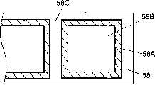
图6A是在制造过程中的触摸屏的平面图,图6B和图6C是在制造过程中触摸屏的截面图。首先形成粘接层56A、56B。然后在此粘接层56A、56B的上面和下面分别贴合剥离膜57A和下剥离膜57B。在它们的内侧夹持着带状的间隔件膜58。然后切下用阴影线表示的框状间隔件部分58A制成间隔件55。6A is a plan view of the touch screen during manufacturing, and FIGS. 6B and 6C are cross-sectional views of the touch screen during manufacturing. First, the
如图6C的截面图所示,在剥离上剥离膜57A和下剥离膜57B之后,通过露出的粘接层56A和56B将间隔件55贴合在上基板52和下基板51的外侧周边上,完成了触摸屏的制作。As shown in the cross-sectional view of FIG. 6C, after peeling off the
这样构成的触摸屏,被安装在前面配置有液晶显示元件的电子设备上,其一对上电极和下电极与设备的电路(未图示)相连接。The touch panel configured in this way is mounted on an electronic device with a liquid crystal display element disposed on the front, and a pair of upper electrodes and lower electrodes thereof are connected to a circuit (not shown) of the device.
在以上的结构中,识别触摸屏背面的液晶显示元件等的显示,用手指或笔尖等对上基板52上面进行按压操作,使上基板52凹陷,按压处的上导电层54和下导电层53接触。由电路依次向上电极和下电极施加电压,通过这些电极之间的电压比,由电路检测出被按压的位置,由此进行各式各样的设备功能的切换。In the above structure, the display of the liquid crystal display element on the back of the touch screen is recognized, and the
作为与本申请的发明关联的先有技术的文献,例如,已知有特开2003-280821号公报。As a prior art document related to the invention of the present application, for example, JP-A-2003-280821 is known.
但是,在如上所述现有的触摸屏中,贴合上基板52和下基板51外侧周边的间隔件55形成为框状,为此,如图6A所示,在制造间隔件55时,作为间隔件55使用的框状间隔件58A以外的内部58B和外部58C都不再使用。浪费了与间隔件58A相比面积很大的上述部分,规定尺寸的带状间隔件膜58可以制作的间隔件55的个数变少。因此,存在间隔件膜58的材料使用率低,触摸屏的成本高昂的问题。However, in the conventional touch screen as described above, the
发明内容Contents of the invention
本发明的目的是提供一种能够解决上述现有问题,较少浪费使用材料,制作容易且价格低廉的触摸屏及其制造方法。The object of the present invention is to provide a touch screen and a manufacturing method thereof which can solve the above existing problems, use less waste materials, and are easy to manufacture and low in price.
为了实现上述目的,本发明设置多个L字状的在上下面形成有粘接层的间隔件的同时,将此多个间隔件贴合在上基板和下基板之间的对向外侧周边上构成的触摸屏。按照此结构,可以由规定尺寸的间隔件膜制造多个间隔件,减少了使用材料的浪费,能够得到容易制造且价格低廉的触摸屏。In order to achieve the above object, the present invention arranges a plurality of L-shaped spacers with adhesive layers formed on the upper and lower surfaces, and sticks the plurality of spacers on the facing outer periphery between the upper substrate and the lower substrate. Composition of the touch screen. According to this configuration, a plurality of spacers can be produced from a spacer film of a predetermined size, and waste of materials used can be reduced, and an easy-to-manufacture and inexpensive touch panel can be obtained.
附图说明Description of drawings
图1是本发明一个实施方式的触摸屏的截面图。FIG. 1 is a cross-sectional view of a touch screen according to an embodiment of the present invention.
图2是本发明一个实施方式的触摸屏的平面图。FIG. 2 is a plan view of a touch panel according to an embodiment of the present invention.
图3是说明本发明一个实施方式的触摸屏的制造方法的平面图和截面图。3 is a plan view and a cross-sectional view illustrating a method of manufacturing a touch panel according to an embodiment of the present invention.
图4是说明本发明一个实施方式的触摸屏的制造方法的另一个截面图。4 is another cross-sectional view illustrating a method of manufacturing a touch panel according to an embodiment of the present invention.
图5是现有的触摸屏的截面图。FIG. 5 is a cross-sectional view of a conventional touch screen.
图6是说明现有的触摸屏制造方法的平面图和截面图。FIG. 6 is a plan view and a cross-sectional view illustrating a conventional touch panel manufacturing method.
具体实施方式Detailed ways
以下,使用图1~图4说明本发明的实施方式。Hereinafter, an embodiment of the present invention will be described using FIGS. 1 to 4 .
为了容易分辨其构成,图1~图4的截面图,放大其在厚度方向上的尺寸表示。对于与背景技术中已经说明结构同样的结构使用同样的符号,并简化其详细说明。In order to easily distinguish its structure, the cross-sectional views of Fig. 1 to Fig. 4 are enlarged to show the size in the thickness direction. The same symbols are used for the same structures as those already described in the background art, and the detailed description thereof is simplified.
图1是本发明一个实施方式的触摸屏的截面图。图2是本发明一个实施方式的触摸屏的平面图。FIG. 1 is a cross-sectional view of a touch screen according to an embodiment of the present invention. FIG. 2 is a plan view of a touch screen according to an embodiment of the present invention.
在图1中,下基板1是玻璃或丙烯酸树脂、聚碳酸酯树脂等具有透光性的基板。上基板2是具有透光性的聚对苯二甲酸乙二酯或聚碳酸酯树脂等薄膜状基板。然后,在下基板1的上面形成有氧化铟锡或氧化锡等具有透光性的下导电层3。同样,在上基板2的下面通过溅镀法等形成上导电层4。In FIG. 1 , the
在下导电层3的上面,由环氧树脂或硅树脂等绝缘树脂以规定的间隔形成有多个点间隔件(未图示)。在上导电层4的两端使用银或碳等形成一对上电极(未图示),在下导电层3的两端,形成与上电极垂直的一对下电极(未图示)。On the upper surface of the lower
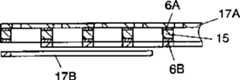
在图2中,间隔件15用无纺布或聚酯薄膜等制成L字状。在一个触摸屏上使用两个间隔件15。第一间隔件15贴在上基板2和下基板1之间的左下侧外周,第二间隔件15与此相对,贴在的右上侧外周。由这两个间隔件使上导电层4和下导电层3保持规定的空隙对向设置。而上导电层4和下导电层3分别经由丙烯酸树脂或橡胶等形成的粘接层6A和6B与间隔件15粘结。In FIG. 2, the
在聚对苯二甲酸乙二酯或聚碳酸酯树脂构成的薄膜状配线基板11的上面或下面,形成由银或碳、铜箔等制造的多个配线图案(未图示)。然后将此配线图案与上电极和下电极连接。再由环氧树脂或丙烯酸树酯、烯烃等密封材料16将左上端和右下端的两个间隔件15的间隙密封。A plurality of wiring patterns (not shown) made of silver, carbon, copper foil, etc. are formed on the upper surface or the lower surface of the film-
下面说明如上所述的间隔件15和触摸屏的制造方法。Next, a method of manufacturing the
图3是说明本发明一个实施方式的触摸屏的制造方法的平面图和截面图。3 is a plan view and a cross-sectional view illustrating a method of manufacturing a touch panel according to an embodiment of the present invention.
如图3A的平面图、图3B的截面图所示,首先在间隔件膜18的上面和下面形成粘接层6A和6B。然后在此粘接层6A和6B的上面和下面,贴合用纸或聚对苯二甲酸乙二酯等构成的上剥离膜17A和下剥离膜17B。在上端和下端以规定的间隔设有贯通孔18B的带状间隔件膜18上,从下面进行半切加工,剩下上剥离膜17A。As shown in the plan view of FIG. 3A and the cross-sectional view of FIG. 3B ,
如图3A所示,通过半切加工,形成用阴影线表示的多个L字状间隔件18A。然后,如图3C的截面图所示,从上剥离膜17A上剥离此间隔件部分18A以外部分的间隔件膜18和下剥离膜17B,在上剥离膜17A的下面形成在左右方向上排列的多个L字状间隔件15。As shown in FIG. 3A , a plurality of L-shaped
最后形成L字状的间隔件15,这些间隔件15按规定的方向排列在间隔件膜18上。如图3A所示,由于能够使多个间隔件15之间的间隔变得很小,所以由一定尺寸的间隔件膜18能够制造出许多间隔件15。结果就能够降低使用材料的浪费,提高使用效率。Finally, L-shaped
在图3A中,为了容易理解其结构,放大了多个间隔件15之间的间隔,以较大的状态表示其间隙。在实际上通过如上所述的半切加工形成多个间隔件15时,由于切刀量只要是具有间隙即可,所以能够以最小的间隔排列出很多的间隔件15。In FIG. 3A , for easy understanding of the structure, the intervals between the plurality of
图4是说明本发明一个实施方式的触摸屏的制造方法的截面图。4 is a cross-sectional view illustrating a method of manufacturing a touch panel according to an embodiment of the present invention.
如图4A的截面图所示,如剥离在左端形成的间隔件15的下剥离膜17B,露出其下面的粘接层6B。然后,如图4B所示,此间隔件15贴在保持在规定组装工具(未图示)上的下基板1的上面,使排列的间隔件15成为平行的状态,比如在左下侧的外侧周边上。此时,在保持下基板1的组装工具上设有突出销等,如果将其插入在间隔件膜18上以一定间隔设置的贯通孔18B中,将间隔件15贴合在下基板1的上面,就可以在下基板1的正确位置上贴上间隔件15而不会出现位置偏差。As shown in the cross-sectional view of FIG. 4A , when the
通过改变为了使上剥离膜17A的下面或下剥离膜17B的上面容易与粘接层6A或6B剥离而涂敷的硅树脂的种类和厚度,使上剥离膜17A与下剥离膜17B的剥离力不同,能够更容易地贴合间隔件15。即,在首先剥离下剥离膜17B时,使下剥离膜17B的剥离力很小,而使上剥离膜17A的剥离力较大。结果如图4A所示,剥离下剥离膜17B时,间隔件15原封不动地贴在剥离力较强的上剥离膜17A上,而不会浮附着在剥离力比较弱的下剥离膜17B一侧,很容易进行下剥离膜17B的剥离。By changing the type and thickness of the silicone resin coated in order to make the lower surface of the
再如图4C所示,将间隔件膜18或下基板1旋转和移动,使排列在下一个的间隔件15的下剥离膜17B剥离。然后,将排列在下一个的间隔件15贴合在下基板1上面的右上侧外周。Further, as shown in FIG. 4C , the
最后,如图4D所示,将下基板1的上面以与上导电层4和下导电层3对向设置的方式重叠上基板2,将下基板1与上基板2的外周边粘合。然后如图1或图2所示,将两个L字状的间隔件15贴在上基板2和下基板1之间的对向外侧周边上,完成了触摸屏的制作。为了密封两个间隔件15之间的间隙涂敷密封材料16、使其干燥,可以在图4C的下基板1上面贴上间隔件15的状态下进行,也可以在完成触摸屏的状态下进行。Finally, as shown in FIG. 4D , the upper surface of the
如此构成的触摸屏,安装在前面配置有液晶显示元件等的电子设备上。一对上电极和下电极由配线基板11的配线图案连接在设备的电路(未图示)上。The touch panel configured in this way is mounted on an electronic device on which a liquid crystal display element and the like are arranged on the front. A pair of upper and lower electrodes is connected to a circuit (not shown) of the device by a wiring pattern of the
在以上的结构中,识别出触摸屏背面的液晶显示元件等的显示,用手指或笔等对上基板2的上面进行按压操作时,上基板2凹陷,在被按压的位置,上导电层4与下导电层3接触。通过电路依次向上电极和下电极上施加电压,由这些电极之间的电压比,通过电路检测出按压的位置,使得设备进行各式各样的功能切换。In the above structure, when the display of the liquid crystal display element on the back of the touch screen is recognized, and the upper surface of the
根据本发明的实施方式,间隔件15做成L字状,多个间隔件15在间隔件膜18上按照一定方向排列,由此能够从规定尺寸的间隔件膜18制造出多个间隔件15,减少了使用材料的浪费,能够提供容易制造且价格低廉的触摸屏及其制造方法。According to the embodiment of the present invention, the
通过用密封材料16将多个L字状间隔件15的间隙密封,可以防止尘埃或水分浸入下导电层3和上导电层4之间的间隙,可以实现下导电层3和上导电层4的稳定接触。By sealing the gaps of a plurality of L-shaped
通过使上剥离膜17A和下剥离膜17B的剥离力不同,可以更容易地将间隔件15贴合在上基板2或下基板1上。By making the peeling force of the
本发明的触摸屏及其制造方法,具有可以提供容易制造且价格低廉的产品的效果,可以应用于各种电子设备的操作中。The touch screen and its manufacturing method of the present invention have the effect of providing an easy-to-manufacture and low-cost product, and can be applied to the operation of various electronic devices.
Claims (6)
Translated fromChineseApplications Claiming Priority (2)
| Application Number | Priority Date | Filing Date | Title |
|---|---|---|---|
| JP2004255210 | 2004-09-02 | ||
| JP2004255210AJP4539241B2 (en) | 2004-09-02 | 2004-09-02 | Touch panel and manufacturing method thereof |
Publications (2)
| Publication Number | Publication Date |
|---|---|
| CN1744021Atrue CN1744021A (en) | 2006-03-08 |
| CN1322408C CN1322408C (en) | 2007-06-20 |
Family
ID=35942392
Family Applications (1)
| Application Number | Title | Priority Date | Filing Date |
|---|---|---|---|
| CNB2005100958308AExpired - Fee RelatedCN1322408C (en) | 2004-09-02 | 2005-09-02 | Touch panel and the manufacturing method |
Country Status (3)
| Country | Link |
|---|---|
| US (1) | US7351922B2 (en) |
| JP (1) | JP4539241B2 (en) |
| CN (1) | CN1322408C (en) |
Cited By (39)
| Publication number | Priority date | Publication date | Assignee | Title |
|---|---|---|---|---|
| CN101770312A (en)* | 2010-03-02 | 2010-07-07 | 友达光电股份有限公司 | Touch control display panel |
| CN101620492B (en)* | 2008-07-04 | 2011-03-30 | 鸿富锦精密工业(深圳)有限公司 | Manufacturing method of touch screen |
| US8105126B2 (en) | 2008-07-04 | 2012-01-31 | Tsinghua University | Method for fabricating touch panel |
| US8111245B2 (en) | 2007-12-21 | 2012-02-07 | Tsinghua University | Touch panel and display device using the same |
| US8115742B2 (en) | 2007-12-12 | 2012-02-14 | Tsinghua University | Touch panel and display device using the same |
| US8125878B2 (en) | 2007-12-27 | 2012-02-28 | Tsinghua University | Touch panel and display device using the same |
| US8199119B2 (en) | 2007-12-12 | 2012-06-12 | Beijing Funate Innovation Technology Co., Ltd. | Touch panel and display device using the same |
| US8237673B2 (en) | 2007-12-14 | 2012-08-07 | Tsinghua University | Touch panel and display device using the same |
| US8237668B2 (en) | 2007-12-27 | 2012-08-07 | Tsinghua University | Touch control device |
| US8237669B2 (en) | 2007-12-27 | 2012-08-07 | Tsinghua University | Touch panel and display device using the same |
| US8237672B2 (en) | 2007-12-14 | 2012-08-07 | Tsinghua University | Touch panel and display device using the same |
| US8237675B2 (en) | 2007-12-27 | 2012-08-07 | Tsinghua University | Touch panel and display device using the same |
| US8237671B2 (en) | 2007-12-12 | 2012-08-07 | Tsinghua University | Touch panel and display device using the same |
| US8237670B2 (en) | 2007-12-12 | 2012-08-07 | Tsinghua University | Touch panel and display device using the same |
| US8237674B2 (en) | 2007-12-12 | 2012-08-07 | Tsinghua University | Touch panel and display device using the same |
| US8243029B2 (en) | 2007-12-14 | 2012-08-14 | Tsinghua University | Touch panel and display device using the same |
| US8243030B2 (en) | 2007-12-21 | 2012-08-14 | Tsinghua University | Touch panel and display device using the same |
| US8248377B2 (en) | 2007-10-23 | 2012-08-21 | Tsinghua University | Touch panel |
| US8248381B2 (en) | 2007-12-12 | 2012-08-21 | Tsinghua University | Touch panel and display device using the same |
| US8248379B2 (en) | 2007-12-14 | 2012-08-21 | Tsinghua University | Touch panel, method for making the same, and display device adopting the same |
| US8248378B2 (en) | 2007-12-21 | 2012-08-21 | Tsinghua University | Touch panel and display device using the same |
| US8248380B2 (en) | 2007-12-14 | 2012-08-21 | Tsinghua University | Touch panel and display device using the same |
| US8253701B2 (en) | 2007-12-14 | 2012-08-28 | Tsinghua University | Touch panel, method for making the same, and display device adopting the same |
| US8253700B2 (en) | 2007-12-14 | 2012-08-28 | Tsinghua University | Touch panel and display device using the same |
| US8260378B2 (en) | 2008-08-22 | 2012-09-04 | Tsinghua University | Mobile phone |
| CN102673086A (en)* | 2012-05-10 | 2012-09-19 | 无锡博一光电科技有限公司 | Bonding method of touch panel and LCD panel |
| US8325146B2 (en) | 2007-12-21 | 2012-12-04 | Tsinghua University | Touch panel and display device using the same |
| US8325145B2 (en) | 2007-12-27 | 2012-12-04 | Tsinghua University | Touch panel and display device using the same |
| US8325585B2 (en) | 2007-12-12 | 2012-12-04 | Tsinghua University | Touch panel and display device using the same |
| US8346316B2 (en) | 2008-08-22 | 2013-01-01 | Tsinghua University | Personal digital assistant |
| US8363017B2 (en) | 2007-12-12 | 2013-01-29 | Beijing Funate Innovation Technology Co., Ltd. | Touch panel and display device using the same |
| US8390580B2 (en) | 2008-07-09 | 2013-03-05 | Tsinghua University | Touch panel, liquid crystal display screen using the same, and methods for making the touch panel and the liquid crystal display screen |
| US8411044B2 (en) | 2007-12-14 | 2013-04-02 | Tsinghua University | Touch panel, method for making the same, and display device adopting the same |
| US8502786B2 (en) | 2007-10-23 | 2013-08-06 | Tsinghua University | Touch panel |
| US8542212B2 (en) | 2007-12-12 | 2013-09-24 | Tsinghua University | Touch panel, method for making the same, and display device adopting the same |
| US8574393B2 (en) | 2007-12-21 | 2013-11-05 | Tsinghua University | Method for making touch panel |
| US8585855B2 (en) | 2007-12-21 | 2013-11-19 | Tsinghua University | Method for making touch panel |
| US9040159B2 (en) | 2007-12-12 | 2015-05-26 | Tsinghua University | Electronic element having carbon nanotubes |
| US9077793B2 (en) | 2009-06-12 | 2015-07-07 | Tsinghua University | Carbon nanotube based flexible mobile phone |
Families Citing this family (7)
| Publication number | Priority date | Publication date | Assignee | Title |
|---|---|---|---|---|
| EP1667183A1 (en)* | 2004-12-01 | 2006-06-07 | IEE INTERNATIONAL ELECTRONICS & ENGINEERING S.A. | Reinforced foil-type switching element |
| US20080185192A1 (en)* | 2007-02-06 | 2008-08-07 | Hsih Lung-Sheng | Touch panel |
| KR100984071B1 (en)* | 2007-03-30 | 2010-09-30 | 후지쯔 콤포넌트 가부시끼가이샤 | Touch panel |
| CN101620454A (en)* | 2008-07-04 | 2010-01-06 | 清华大学 | Potable computer |
| CN101676832B (en)* | 2008-09-19 | 2012-03-28 | 清华大学 | Desktop PC |
| CN101470564B (en)* | 2007-12-28 | 2011-06-08 | 财团法人工业技术研究院 | Touch panel and manufacturing method thereof |
| CN114126207B (en)* | 2020-08-27 | 2024-03-26 | 致伸科技股份有限公司 | Thin film circuit board and production method thereof |
Family Cites Families (14)
| Publication number | Priority date | Publication date | Assignee | Title |
|---|---|---|---|---|
| US4958148A (en)* | 1985-03-22 | 1990-09-18 | Elmwood Sensors, Inc. | Contrast enhancing transparent touch panel device |
| US4786767A (en)* | 1987-06-01 | 1988-11-22 | Southwall Technologies Inc. | Transparent touch panel switch |
| JPH02105916A (en)* | 1988-10-14 | 1990-04-18 | Canon Inc | touch panel input device |
| JP2545233Y2 (en)* | 1990-07-09 | 1997-08-25 | カシオ計算機株式会社 | Key input device |
| JPH0927243A (en)* | 1995-07-13 | 1997-01-28 | Hitachi Aic Inc | Touch screen |
| TW388894B (en)* | 1997-10-09 | 2000-05-01 | Nissha Printing | High strength touch panel and manufacturing method therefor |
| JP4596687B2 (en)* | 2000-07-27 | 2010-12-08 | 富士通コンポーネント株式会社 | PANEL TYPE PERIPHERAL DEVICE, ITS MANUFACTURING METHOD, AND PANEL JIG FOR MANUFACTURING THE SAME |
| US6587097B1 (en)* | 2000-11-28 | 2003-07-01 | 3M Innovative Properties Co. | Display system |
| JP2002202855A (en)* | 2000-12-28 | 2002-07-19 | Matsushita Electric Ind Co Ltd | Touch panel and electronic device using the same |
| JP4055378B2 (en)* | 2001-07-06 | 2008-03-05 | 松下電器産業株式会社 | Touch panel switch |
| TWI224276B (en)* | 2001-11-02 | 2004-11-21 | Matsushita Electric Industrial Co Ltd | Touch panel and method of manufacturing the same |
| JP4066641B2 (en)* | 2001-11-20 | 2008-03-26 | 松下電器産業株式会社 | Touch panel |
| JP2003280821A (en) | 2002-03-26 | 2003-10-02 | Matsushita Electric Ind Co Ltd | Light transmissive touch panel |
| JP3960850B2 (en)* | 2002-04-26 | 2007-08-15 | ホシデン株式会社 | Touch panel |
- 2004
- 2004-09-02JPJP2004255210Apatent/JP4539241B2/ennot_activeExpired - Fee Related
- 2005
- 2005-07-27USUS11/191,798patent/US7351922B2/ennot_activeExpired - Fee Related
- 2005-09-02CNCNB2005100958308Apatent/CN1322408C/ennot_activeExpired - Fee Related
Cited By (48)
| Publication number | Priority date | Publication date | Assignee | Title |
|---|---|---|---|---|
| US8248377B2 (en) | 2007-10-23 | 2012-08-21 | Tsinghua University | Touch panel |
| US8502786B2 (en) | 2007-10-23 | 2013-08-06 | Tsinghua University | Touch panel |
| US8363017B2 (en) | 2007-12-12 | 2013-01-29 | Beijing Funate Innovation Technology Co., Ltd. | Touch panel and display device using the same |
| US8325585B2 (en) | 2007-12-12 | 2012-12-04 | Tsinghua University | Touch panel and display device using the same |
| US8115742B2 (en) | 2007-12-12 | 2012-02-14 | Tsinghua University | Touch panel and display device using the same |
| US9040159B2 (en) | 2007-12-12 | 2015-05-26 | Tsinghua University | Electronic element having carbon nanotubes |
| US8199119B2 (en) | 2007-12-12 | 2012-06-12 | Beijing Funate Innovation Technology Co., Ltd. | Touch panel and display device using the same |
| US8237671B2 (en) | 2007-12-12 | 2012-08-07 | Tsinghua University | Touch panel and display device using the same |
| US8237670B2 (en) | 2007-12-12 | 2012-08-07 | Tsinghua University | Touch panel and display device using the same |
| US8542212B2 (en) | 2007-12-12 | 2013-09-24 | Tsinghua University | Touch panel, method for making the same, and display device adopting the same |
| US8248381B2 (en) | 2007-12-12 | 2012-08-21 | Tsinghua University | Touch panel and display device using the same |
| US8237674B2 (en) | 2007-12-12 | 2012-08-07 | Tsinghua University | Touch panel and display device using the same |
| US8248380B2 (en) | 2007-12-14 | 2012-08-21 | Tsinghua University | Touch panel and display device using the same |
| US8243029B2 (en) | 2007-12-14 | 2012-08-14 | Tsinghua University | Touch panel and display device using the same |
| US8237673B2 (en) | 2007-12-14 | 2012-08-07 | Tsinghua University | Touch panel and display device using the same |
| US8237672B2 (en) | 2007-12-14 | 2012-08-07 | Tsinghua University | Touch panel and display device using the same |
| US8253700B2 (en) | 2007-12-14 | 2012-08-28 | Tsinghua University | Touch panel and display device using the same |
| US8248379B2 (en) | 2007-12-14 | 2012-08-21 | Tsinghua University | Touch panel, method for making the same, and display device adopting the same |
| US8411044B2 (en) | 2007-12-14 | 2013-04-02 | Tsinghua University | Touch panel, method for making the same, and display device adopting the same |
| US8253701B2 (en) | 2007-12-14 | 2012-08-28 | Tsinghua University | Touch panel, method for making the same, and display device adopting the same |
| US8574393B2 (en) | 2007-12-21 | 2013-11-05 | Tsinghua University | Method for making touch panel |
| US8325146B2 (en) | 2007-12-21 | 2012-12-04 | Tsinghua University | Touch panel and display device using the same |
| US8243030B2 (en) | 2007-12-21 | 2012-08-14 | Tsinghua University | Touch panel and display device using the same |
| US8248378B2 (en) | 2007-12-21 | 2012-08-21 | Tsinghua University | Touch panel and display device using the same |
| US8111245B2 (en) | 2007-12-21 | 2012-02-07 | Tsinghua University | Touch panel and display device using the same |
| US8585855B2 (en) | 2007-12-21 | 2013-11-19 | Tsinghua University | Method for making touch panel |
| US8237669B2 (en) | 2007-12-27 | 2012-08-07 | Tsinghua University | Touch panel and display device using the same |
| US8325145B2 (en) | 2007-12-27 | 2012-12-04 | Tsinghua University | Touch panel and display device using the same |
| US8125878B2 (en) | 2007-12-27 | 2012-02-28 | Tsinghua University | Touch panel and display device using the same |
| US8237675B2 (en) | 2007-12-27 | 2012-08-07 | Tsinghua University | Touch panel and display device using the same |
| US8237668B2 (en) | 2007-12-27 | 2012-08-07 | Tsinghua University | Touch control device |
| US8228308B2 (en) | 2008-07-04 | 2012-07-24 | Tsinghua University | Method for making liquid crystal display adopting touch panel |
| US8199123B2 (en) | 2008-07-04 | 2012-06-12 | Tsinghua University | Method for making liquid crystal display screen |
| US8237677B2 (en) | 2008-07-04 | 2012-08-07 | Tsinghua University | Liquid crystal display screen |
| US8237680B2 (en) | 2008-07-04 | 2012-08-07 | Tsinghua University | Touch panel |
| US8105126B2 (en) | 2008-07-04 | 2012-01-31 | Tsinghua University | Method for fabricating touch panel |
| CN101620492B (en)* | 2008-07-04 | 2011-03-30 | 鸿富锦精密工业(深圳)有限公司 | Manufacturing method of touch screen |
| US8237679B2 (en) | 2008-07-04 | 2012-08-07 | Tsinghua University | Liquid crystal display screen |
| US8411051B2 (en) | 2008-07-09 | 2013-04-02 | Tsinghua University | Liquid crystal display screen |
| US8411052B2 (en) | 2008-07-09 | 2013-04-02 | Tsinghua University | Touch panel, liquid crystal display screen using the same, and methods for making the touch panel and the liquid crystal display screen |
| US8390580B2 (en) | 2008-07-09 | 2013-03-05 | Tsinghua University | Touch panel, liquid crystal display screen using the same, and methods for making the touch panel and the liquid crystal display screen |
| US8346316B2 (en) | 2008-08-22 | 2013-01-01 | Tsinghua University | Personal digital assistant |
| US8260378B2 (en) | 2008-08-22 | 2012-09-04 | Tsinghua University | Mobile phone |
| US9077793B2 (en) | 2009-06-12 | 2015-07-07 | Tsinghua University | Carbon nanotube based flexible mobile phone |
| CN101770312A (en)* | 2010-03-02 | 2010-07-07 | 友达光电股份有限公司 | Touch control display panel |
| CN101770312B (en)* | 2010-03-02 | 2012-07-04 | 友达光电股份有限公司 | Touch control display panel |
| CN102673086B (en)* | 2012-05-10 | 2014-12-17 | 无锡博一光电科技有限公司 | Method for attaching touch panel and LCD panel |
| CN102673086A (en)* | 2012-05-10 | 2012-09-19 | 无锡博一光电科技有限公司 | Bonding method of touch panel and LCD panel |
Also Published As
| Publication number | Publication date |
|---|---|
| JP2006072693A (en) | 2006-03-16 |
| CN1322408C (en) | 2007-06-20 |
| JP4539241B2 (en) | 2010-09-08 |
| US20060044284A1 (en) | 2006-03-02 |
| US7351922B2 (en) | 2008-04-01 |
Similar Documents
| Publication | Publication Date | Title |
|---|---|---|
| CN1744021A (en) | Touch screen and manufacturing method thereof | |
| TWI428796B (en) | Touch panel and manufacturing method thereof | |
| JP5611864B2 (en) | Input device and method for manufacturing input device | |
| EP2703963B1 (en) | Spacer-less input device | |
| JP4711150B2 (en) | Touch panel and display device | |
| CN101075169A (en) | Touch panel | |
| CN1885250B (en) | Touch panel and manufacturing method for the same | |
| CN101446881B (en) | touch screen | |
| CN106155403B (en) | Touch control element | |
| CN1465005A (en) | Transparent touch panel and method of manufacturing the touch panel | |
| CN1815310A (en) | Pressure sensitive conductive sheet, method of manufacturing the same, and touch panel using the same | |
| CN101110010A (en) | touch panel | |
| CN100465870C (en) | touch panel | |
| CN1728060A (en) | input device | |
| CN100345095C (en) | Transparent touch panel | |
| CN101059740A (en) | Touch panel and manufacturing method thereof | |
| CN1967457A (en) | Touch panel, method of manufacturing the same, and input device using the same | |
| TWI471798B (en) | Input device | |
| KR20150134010A (en) | Touch window | |
| CN1794155A (en) | Touch screen | |
| KR100510723B1 (en) | Touch Panel with Liquid Crystal Display Device | |
| CN100365479C (en) | Touch screen with protective film and manufacturing method thereof | |
| CN209946863U (en) | Touch screen and touch screen terminal | |
| JPH0418628A (en) | Touch panel | |
| WO2011036996A1 (en) | Coordinate-input device, and electronic equipment and display device provided with said coordinate-input device |
Legal Events
| Date | Code | Title | Description |
|---|---|---|---|
| C06 | Publication | ||
| PB01 | Publication | ||
| C10 | Entry into substantive examination | ||
| SE01 | Entry into force of request for substantive examination | ||
| C14 | Grant of patent or utility model | ||
| GR01 | Patent grant | ||
| CF01 | Termination of patent right due to non-payment of annual fee | Granted publication date:20070620 Termination date:20150902 | |
| EXPY | Termination of patent right or utility model |