CN1737982A - Plasma display panel and manufacturing method thereof - Google Patents
Plasma display panel and manufacturing method thereofDownload PDFInfo
- Publication number
- CN1737982A CN1737982ACNA2005100928073ACN200510092807ACN1737982ACN 1737982 ACN1737982 ACN 1737982ACN A2005100928073 ACNA2005100928073 ACN A2005100928073ACN 200510092807 ACN200510092807 ACN 200510092807ACN 1737982 ACN1737982 ACN 1737982A
- Authority
- CN
- China
- Prior art keywords
- discharge
- electrodes
- dielectric
- electrode
- display panel
- Prior art date
- Legal status (The legal status is an assumption and is not a legal conclusion. Google has not performed a legal analysis and makes no representation as to the accuracy of the status listed.)
- Pending
Links
- 238000004519manufacturing processMethods0.000titleclaimsabstractdescription8
- 239000000758substrateSubstances0.000claimsabstractdescription76
- OAICVXFJPJFONN-UHFFFAOYSA-NPhosphorusChemical compound[P]OAICVXFJPJFONN-UHFFFAOYSA-N0.000claimsabstractdescription22
- 230000004888barrier functionEffects0.000claimsdescription28
- 239000010410layerSubstances0.000claimsdescription26
- 239000007789gasSubstances0.000claimsdescription25
- 238000000034methodMethods0.000claimsdescription21
- 239000000463materialSubstances0.000claimsdescription13
- 238000000059patterningMethods0.000claimsdescription6
- 239000011241protective layerSubstances0.000claimsdescription6
- 238000001035dryingMethods0.000claimsdescription4
- 239000002994raw materialSubstances0.000description6
- 239000011159matrix materialSubstances0.000description4
- 239000011521glassSubstances0.000description3
- 206010047571Visual impairmentDiseases0.000description2
- 230000005684electric fieldEffects0.000description2
- 239000002245particleSubstances0.000description2
- 230000002085persistent effectEffects0.000description2
- 230000005855radiationEffects0.000description2
- 229910004283SiO 4Inorganic materials0.000description1
- 230000005540biological transmissionEffects0.000description1
- 230000015572biosynthetic processEffects0.000description1
- 239000003086colorantSubstances0.000description1
- 230000007423decreaseEffects0.000description1
- 230000000694effectsEffects0.000description1
- 230000005284excitationEffects0.000description1
- 239000000945fillerSubstances0.000description1
- 239000003292glueSubstances0.000description1
- 238000002347injectionMethods0.000description1
- 239000007924injectionSubstances0.000description1
- 238000004969ion scattering spectroscopyMethods0.000description1
- 238000004904shorteningMethods0.000description1
- 239000005361soda-lime glassSubstances0.000description1
- 238000006467substitution reactionMethods0.000description1
Images


Classifications
- H—ELECTRICITY
- H01—ELECTRIC ELEMENTS
- H01J—ELECTRIC DISCHARGE TUBES OR DISCHARGE LAMPS
- H01J11/00—Gas-filled discharge tubes with alternating current induction of the discharge, e.g. alternating current plasma display panels [AC-PDP]; Gas-filled discharge tubes without any main electrode inside the vessel; Gas-filled discharge tubes with at least one main electrode outside the vessel
- H01J11/20—Constructional details
- H01J11/34—Vessels, containers or parts thereof, e.g. substrates
- H01J11/36—Spacers, barriers, ribs, partitions or the like
- H—ELECTRICITY
- H01—ELECTRIC ELEMENTS
- H01J—ELECTRIC DISCHARGE TUBES OR DISCHARGE LAMPS
- H01J11/00—Gas-filled discharge tubes with alternating current induction of the discharge, e.g. alternating current plasma display panels [AC-PDP]; Gas-filled discharge tubes without any main electrode inside the vessel; Gas-filled discharge tubes with at least one main electrode outside the vessel
- H01J11/10—AC-PDPs with at least one main electrode being out of contact with the plasma
- H01J11/16—AC-PDPs with at least one main electrode being out of contact with the plasma with main electrodes provided inside or on the side face of the spacers
- H—ELECTRICITY
- H01—ELECTRIC ELEMENTS
- H01J—ELECTRIC DISCHARGE TUBES OR DISCHARGE LAMPS
- H01J11/00—Gas-filled discharge tubes with alternating current induction of the discharge, e.g. alternating current plasma display panels [AC-PDP]; Gas-filled discharge tubes without any main electrode inside the vessel; Gas-filled discharge tubes with at least one main electrode outside the vessel
- H01J11/20—Constructional details
- H01J11/22—Electrodes, e.g. special shape, material or configuration
- H01J11/24—Sustain electrodes or scan electrodes
- H—ELECTRICITY
- H01—ELECTRIC ELEMENTS
- H01J—ELECTRIC DISCHARGE TUBES OR DISCHARGE LAMPS
- H01J11/00—Gas-filled discharge tubes with alternating current induction of the discharge, e.g. alternating current plasma display panels [AC-PDP]; Gas-filled discharge tubes without any main electrode inside the vessel; Gas-filled discharge tubes with at least one main electrode outside the vessel
- H01J11/20—Constructional details
- H01J11/22—Electrodes, e.g. special shape, material or configuration
- H01J11/26—Address electrodes
- H—ELECTRICITY
- H01—ELECTRIC ELEMENTS
- H01J—ELECTRIC DISCHARGE TUBES OR DISCHARGE LAMPS
- H01J11/00—Gas-filled discharge tubes with alternating current induction of the discharge, e.g. alternating current plasma display panels [AC-PDP]; Gas-filled discharge tubes without any main electrode inside the vessel; Gas-filled discharge tubes with at least one main electrode outside the vessel
- H01J11/20—Constructional details
- H01J11/54—Means for exhausting the gas
- H—ELECTRICITY
- H01—ELECTRIC ELEMENTS
- H01J—ELECTRIC DISCHARGE TUBES OR DISCHARGE LAMPS
- H01J2211/00—Plasma display panels with alternate current induction of the discharge, e.g. AC-PDPs
- H01J2211/20—Constructional details
- H01J2211/34—Vessels, containers or parts thereof, e.g. substrates
- H01J2211/36—Spacers, barriers, ribs, partitions or the like
- H01J2211/361—Spacers, barriers, ribs, partitions or the like characterized by the shape
- H01J2211/363—Cross section of the spacers
Landscapes
- Engineering & Computer Science (AREA)
- Physics & Mathematics (AREA)
- Plasma & Fusion (AREA)
- Chemical & Material Sciences (AREA)
- Materials Engineering (AREA)
- Gas-Filled Discharge Tubes (AREA)
Abstract
Description
Translated fromChinese与相关申请的交叉引用Cross References to Related Applications
本申请要求2004年8月18日在韩国知识产权局申请的韩国专利10-2004-0065038的优先权,在此将其公开全部引入作为参考。This application claims priority to Korean Patent No. 10-2004-0065038 filed with the Korean Intellectual Property Office on Aug. 18, 2004, the disclosure of which is hereby incorporated by reference in its entirety.
技术领域technical field
本发明涉及等离子体显示面板,更具体地说,涉及包括介质墙的等离子体显示面板及其制造方法,其中该介质墙覆盖沿着放电室周边设置的放电电极。The present invention relates to a plasma display panel, and more particularly, to a plasma display panel including a dielectric wall covering discharge electrodes disposed along the peripheries of discharge cells, and a manufacturing method thereof.
背景技术Background technique
总地来说,等离子体显示面板是平板显示设备,其中放电气体注入两个基板之间以产生放电。荧光粉层被放电产生的紫外线激发,以显示希望的数字、字符和图像。In general, a plasma display panel is a flat panel display device in which a discharge gas is injected between two substrates to generate a discharge. The phosphor layer is excited by the ultraviolet rays generated by the discharge to display desired numbers, characters and images.
参见图1,常规的等离子体显示面板100包括前基板110、面向前基板110的后基板120、设置在前基板110内表面的X电极131和Y电极134。面板100还包括覆盖X和Y电极131和134的前介电层140、涂覆在前介电层140上的保护层150、形成在后基板120的内表面上的寻址电极160。面板100进一步包括覆盖寻址电极160的后介电层170、设置在前后基板110和120之间的障壁180、以及形成在障壁180中的红、绿和蓝荧光粉层190。Referring to FIG. 1 , a conventional
X电极131包括第一透明电极线132和形成在第一透明电极线132上的第一汇流电极线133。Y电极134包括第二透明电极线135和形成在第二透明电极线135上的第二汇流电极线136。The
在包括上述结构的等离子体显示面板100中,电信号施加到Y电极134和寻址电极160,以选择放电室。一旦选择了放电室,电信号就交替施加到X和Y电极131和134,以从前基板110的内表面产生表面放电并产生紫外辐射。可见光从所选择的放电室里的荧光粉层190发射,以显示静止的图像或活动的图片。In the
一旦基板110和120以及障壁180被组装,则真空排气过程就通过i)典型地限定在后基板120内的孔(未示出)和ii)连接到该孔的管(未示出;典型地是玻璃管)被执行,以从面板100的内部排除不纯的气体。孔和管也被用作注入放电气体,并且气体注入后孔就被密封。在常规的显示面板100中,矩阵形的障壁180限定了放电室,并且放电室有四个封闭的侧。此外,在前基板110的较低部分和障壁180的上端部之间几乎没有空间。这种“紧密装配”结构使从前基板110的中心部分(指向障壁180)排除不纯的气体变得困难,而在前基板110的中心部分由于真空排气过程中在该区域未提供不纯气体的排气路径,所以通常会产生大量不纯的气体。Once the
因此,在真空排气过程中不能充分执行不纯气体的排放。因此,不纯气体保留在面板100内,因此缩短面板100的寿命,并且可能产生诸如持久残留图像和不稳定放电的问题。Therefore, the discharge of impure gas cannot be sufficiently performed during vacuum evacuation. Accordingly, impure gas remains inside the
此外,放电从X和Y电极131和134之间的放电间隙开始,并向X和Y电极131和134的外部扩散。这样,放电沿着前基板110的平面扩散,导致放电室的空间利用率低。In addition, the discharge starts from the discharge gap between the X and
由于X电极131、Y电极134、前介电层140和保护层150形成在前基板110的内表面上,所以可见光的能见度甚至达不到60%。因此,明度降低。Since the
在等离子体显示面板100长时间被驱动的情况下,放电向荧光粉层190扩散。因此,由于电场而喷射到荧光粉层190的放电气体的带电粒子造成持久的残留图像。When the
此外,当10%体积或更多的高浓度Xe气填充放电室时,电子的离子化和激发引起激子的产生,这样,明度和放电效率增加。然而,由于使用高浓度Xe气,初始放电点火电压变高。In addition, when the discharge cell is filled with high-concentration Xe gas of 10% by volume or more, ionization and excitation of electrons cause excitons to be generated, thus increasing brightness and discharge efficiency. However, due to the use of high-concentration Xe gas, the initial discharge ignition voltage becomes high.
发明内容Contents of the invention
本发明一方面提供一种能通过沿着放电室的周边设置放电电极并在放电室的对角方向产生相对放电来提高放电效率的等离子体显示面板,并提供一种制造该等离子体显示面板的方法。One aspect of the present invention provides a plasma display panel capable of improving discharge efficiency by arranging discharge electrodes along the periphery of the discharge cells and generating relative discharges in diagonal directions of the discharge cells, and provides a method for manufacturing the plasma display panel method.
本发明另一方面提供一种等离子体显示面板,其中通过在基板和介质墙之间形成空隙,可以充分执行排气过程。Another aspect of the present invention provides a plasma display panel in which an exhaust process can be sufficiently performed by forming a gap between a substrate and a dielectric wall.
本发明另一方面提供一种能通过将Y电极和寻址电极覆盖在介质墙中而执行高速寻址过程的等离子体显示面板。Another aspect of the present invention provides a plasma display panel capable of performing a high-speed addressing process by covering Y electrodes and address electrodes in a dielectric wall.
本发明另一方面提供一种等离子体显示面板。在一个实施例中,该面板包括i)前基板;ii)面向该前基板设置的后基板;iii)设置在所述前后基板之间以和所述前后基板一起限定放电室的介质墙,并且其具有彼此高度不同的部分;iv)包括X电极和Y电极的维持放电电极对,其嵌入所述介质墙内并围绕所述放电室的放电角设置;v)嵌入所述介质墙并沿着与所述Y电极交叉的方向设置的寻址电极;和vi)形成在所述放电室内的红、绿和蓝荧光粉层。Another aspect of the present invention provides a plasma display panel. In one embodiment, the panel comprises i) a front substrate; ii) a rear substrate disposed facing the front substrate; iii) a dielectric wall disposed between the front and rear substrates to define discharge cells together with the front and rear substrates, and It has parts different in height from each other; iv) a sustain discharge electrode pair including an X electrode and a Y electrode, which is embedded in the dielectric wall and arranged around the discharge corner of the discharge cell; v) embedded in the dielectric wall and arranged along address electrodes disposed in a direction crossing the Y electrodes; and vi) red, green and blue phosphor layers formed in the discharge cells.
在一个实施例中,所述介质墙可以包括沿着所述面板的一个方向设置的第一介质墙,和从相邻的第一介质墙延伸以与所述第一介质墙交叉的第二介质墙,并且所述第一介质墙的高度可以低于所述第二介质墙的高度。In one embodiment, the dielectric walls may include a first dielectric wall disposed along one direction of the panel, and a second dielectric wall extending from an adjacent first dielectric wall to cross the first dielectric wall. wall, and the height of the first dielectric wall may be lower than the height of the second dielectric wall.
在一个实施例中,所述寻址电极可以设置在所述第二介质墙内大致与第二介质墙平行,并且可以不设置在所述第一介质墙内。In one embodiment, the address electrodes may be arranged in the second dielectric wall substantially parallel to the second dielectric wall, and may not be arranged in the first dielectric wall.
在一个实施例中,可以在所述第一介质墙和所述前基板之间形成预定间隙,以提供不纯气体的排气路径。In one embodiment, a predetermined gap may be formed between the first dielectric wall and the front substrate to provide an exhaust path for impure gas.
在一个实施例中,所述X电极可以设置成围绕放电室的第一放电角,并且所述Y电极可以设置成围绕所述放电室内第一放电角的对角方向处的第二放电角。In one embodiment, the X electrodes may be disposed to surround a first discharge angle of the discharge cell, and the Y electrodes may be disposed to surround a second discharge angle in a diagonal direction of the first discharge angle within the discharge chamber.
在一个实施例中,所述X和Y电极可以设置在同一平面内,并且所述寻址电极可以设置在所述Y电极的上部或下部。In one embodiment, the X and Y electrodes may be disposed in the same plane, and the address electrodes may be disposed above or below the Y electrodes.
本发明的另一方面还提供一种制造等离子体显示面板的方法。在一个实施例中,该方法包括i)准备透明基板;ii)在该基板上形成X电极和Y电极;iii)图形化用于形成第一介质墙的原料,以覆盖所述第一介质墙内的X和Y电极;iv)干燥和烘烤用于所述第一介质墙的原料;v)沿着与所述Y电极交叉的方向在所述第一介质墙的原料上图形化寻址电极;vi)图形化用于形成第二介质墙的原料,以覆盖所述寻址电极;和vii)干燥和烘烤用于所述第二介质墙的原料,以形成彼此具有不同高度的所述第一介质墙和第二介质墙。Another aspect of the present invention also provides a method of manufacturing a plasma display panel. In one embodiment, the method includes i) preparing a transparent substrate; ii) forming X electrodes and Y electrodes on the substrate; iii) patterning the raw material for forming the first dielectric wall to cover the first dielectric wall X and Y electrodes within; iv) drying and baking the material for the first dielectric wall; v) patterning addressing on the material of the first dielectric wall along a direction crossing the Y electrodes electrodes; vi) patterning the raw material for forming the second dielectric wall to cover the address electrodes; and vii) drying and baking the raw material for the second dielectric wall to form all the raw materials having different heights from each other Describe the first dielectric wall and the second dielectric wall.
在一个实施例中,所述X和Y电极可以沿着放电室的周边设置,以围绕放电室内彼此成对角线的所述放电角。In one embodiment, the X and Y electrodes may be disposed along the periphery of the discharge chamber to surround the discharge corners that are diagonal to each other within the discharge chamber.
在一个实施例中,寻址电极可以沿着放电室的周边设置,并可以沿着与所述Y电极交叉的方向形成在Y电极的上部。In one embodiment, the address electrodes may be disposed along the periphery of the discharge cells, and may be formed on top of the Y electrodes along a direction crossing the Y electrodes.
在一个实施例中,由于在烘烤过程中的收缩,未形成所述寻址电极处的介质墙的高度可以低于形成所述寻址电极处的介质墙的高度。In one embodiment, due to shrinkage during baking, the height of the dielectric wall where the address electrodes are not formed may be lower than the height of the dielectric walls where the address electrodes are formed.
附图说明Description of drawings
下面参照附图描述本发明的实施例。Embodiments of the present invention are described below with reference to the drawings.
图1是常规等离子体显示面板的分解透视图。FIG. 1 is an exploded perspective view of a conventional plasma display panel.
图2是根据本发明第一实施例的等离子体显示面板的分解透视图。FIG. 2 is an exploded perspective view of a plasma display panel according to a first embodiment of the present invention.
图3是图2所示的放电电极的布置平面图。FIG. 3 is a plan view of the arrangement of discharge electrodes shown in FIG. 2 .
图4是图2所示的放电电极的分解透视图。FIG. 4 is an exploded perspective view of the discharge electrode shown in FIG. 2 .
图5是图2的等离子体显示面板在面板彼此连接处沿着I-I线的横截面图。5 is a cross-sectional view of the plasma display panel of FIG. 2 along line I-I where the panels are connected to each other.
图6是根据本发明第二实施例的等离子体显示面板的横截面图。6 is a cross-sectional view of a plasma display panel according to a second embodiment of the present invention.
具体实施方式Detailed ways
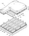
图2示出根据本发明一个实施例的等离子体显示面板200的一部分。FIG. 2 illustrates a portion of a
参见图2,等离子体显示面板200包括前基板210以及与前基板210平行设置的后基板220。Referring to FIG. 2 , the
前基板210一般由例如钠钙玻璃的透明基板形成。后基板220典型地由与前基板210相同的材料形成。The front substrate 210 is generally formed of a transparent substrate such as soda lime glass. The rear substrate 220 is typically formed of the same material as the front substrate 210 .
介质墙230设置在前基板210与后基板220之间,并和前后基板210和220一起限定了放电室。在一个实施例中,介质墙230通过在玻璃浆中添加多种填充物形成。The
在一个实施例中,介质墙230包括沿着面板200的X方向设置的第一介质墙231和沿着面板200的Y方向设置的第二介质墙232。在一个实施例中,第一介质墙231从相邻对的第二介质墙232的内壁向彼此延伸,并且相连的第一和第二介质墙231和232形成矩阵形。In one embodiment, the
在另一个实施例中,介质墙230可以形成弯曲形、△形、六角形或蜂窝形。在一个实施例中,被介质墙230限定的放电室如果限定放电空间,则可以形成其它的多边形或者形成圆形。In another embodiment, the
形成维持放电电极对的X电极240和Y电极250以及寻址电极260嵌入介质墙230中。在一个实施例中,X电极240、Y电极250和寻址电极260沿着放电室的周边设置,并且电极240-260彼此电绝缘。
由例如MgO形成的保护层270沉积在介质墙230的内表面上,以发射二次电子。A
障壁280形成在介质墙230和后基板220之间。在一个实施例中,不同于介质墙230,障壁280由低介电常数的材料形成。在一个实施例中,障壁280在对应于介质墙230的部分形成与介质墙230相同的形状。Barrier ribs 280 are formed between the
也就是,障壁280包括与第一介质墙231(X方向)平行设置的第一障壁281和与第二介质墙232(Y方向)平行设置的第二障壁282。在一个实施例中,第一和第二障壁281和282形成矩阵形。That is, the barrier ribs 280 include a first barrier rib 281 disposed parallel to the first dielectric wall 231 (X direction) and a second barrier rib 282 disposed parallel to the second dielectric wall 232 (Y direction). In one embodiment, the first and second barrier ribs 281 and 282 form a matrix shape.
在一个实施例中,如果仅介质墙230形成在前后基板210和220之间,放电室就被单一壁所限定。在另一个实施例中,如图2,如果介质墙230和障壁280形成在前后基板210和220之间,则放电室就被具有不同介电性质的材料形成的双壁所限定。In one embodiment, if only the
放电气体例如Ne-Xe或He-Xe被注入被前基板210、后基板220、介质墙230和障壁280限定的放电室内。A discharge gas such as Ne—Xe or He—Xe is injected into the discharge chamber defined by the front substrate 210 , the rear substrate 220 , the
由放电气体产生的紫外线所激发的红、绿和蓝荧光粉层290形成在放电室内。在一个实施例中,每个荧光粉层290都可以涂覆在放电室内的任何地方。在另一个实施例中,荧光粉层290以本实施例中的预定厚度涂覆在障壁280的内壁上和放电室的上表面上。Red, green and blue phosphor layers 290 excited by ultraviolet rays generated by the discharge gas are formed within the discharge cells. In one embodiment, each phosphor layer 290 can be applied anywhere within the discharge chamber. In another embodiment, the phosphor layer 290 is coated on the inner wall of the barrier rib 280 and the upper surface of the discharge cell with a predetermined thickness in this embodiment.
红、绿或蓝荧光粉层290涂覆在每个放电室上。在一个实施例中,红荧光粉层由(Y,Gd)BO3:Eu3+形成,绿荧光粉层由Zn2SiO4:Mn2+形成,而蓝荧光粉层由BaMgAl10O17:Eu2+形成。A red, green or blue phosphor layer 290 is coated on each discharge cell. In one embodiment, the red phosphor layer is formed of (Y,Gd)BO3 :Eu3+ , the green phosphor layer is formed of Zn2 SiO4 :Mn2+ , and the blue phosphor layer is formed of BaMgAl10 O17 : Eu2+ formation.
在一个实施例中,维持放电电极对,也就是X和Y电极240和250,在放电室内成对角线地产生放电。在本实施例中,寻址电极260沿着与Y电极250交叉的方向设置在Y电极250的上部或下部,并且第一和第二介质墙231和232的高度彼此不同。In one embodiment, the pair of sustain discharge electrodes, that is, the X and
图3是图2的放电电极的平面图,图4是图3的放电电极的透视图,而图5是面板沿着图3的I-I线的横截面图。3 is a plan view of the discharge electrode of FIG. 2, FIG. 4 is a perspective view of the discharge electrode of FIG. 3, and FIG. 5 is a cross-sectional view of the panel along line I-I of FIG.
参见图3至图5,等离子体显示面板200包括第一介质墙231和连接在第一介质墙231上的第二介质墙232。在一个实施例中,通过连接第一和第二介质墙231和232形成的放电室310被形成为方形。在一个实施例中,放电室310以彼此间的恒定间隔沿着面板200的X和Y方向连续设置。Referring to FIGS. 3 to 5 , the
X和Y电极240和250以及寻址电极260嵌入介质墙230内。X电极240被设置成围绕放电室310的第一放电角311,而Y电极250被设置成围绕与第一放电角311对角的第二放电角312。此外,寻址电极260与Y电极1250交叉设置。X and
X电极240包括沿着放电室310的X方向设置的X电极线241。在一个实施例中,X电极线241形成带状。在一个实施例中,一条X电极线241设置在每个第一介质墙231内,并且可以局部地具有不同的体积,以减少线阻抗。The
X电极突起242沿着放电室310的Y方向从X电极线241突起。在一个实施例中,X电极突起242从X电极线241整体地形成。X电极突起242的长度与放电室310在Y方向上的一侧一致。一个X电极突起242设置在每个第二介质墙232处。The
在一个实施例中,通过连接X电极线241和X电极突起242,X电极240沿着放电室310的X方向形成梳状。In one embodiment, the
Y电极250从放电室310的面对X电极240的一侧沿着平行于X电极240的方向设置。The
Y电极250包括沿着放电室310的X方向设置的Y电极线251。Y电极线251设置在每一个放电室310处,并与X电极线241成对,并且设置在放电室310内的X电极线241的相对侧。在一个实施例中,Y电极线251形成带状,并且一条Y电极线251设置在每个第一介质墙231内。The
Y电极突起252沿着放电室310的Y方向从Y电极线251突起。在一个实施例中,Y电极突起252从Y电极线251整体地形成。Y电极突起252的长度与放电室310在Y方向上的一侧一致。一个Y电极突起252设置在每个第二介质墙232处。The
如上所述,Y电极线251和Y电极突起252彼此连接,这样,Y电极250就沿着放电室310的X方向形成梳状。As described above, the
在一个实施例中,X电极线241和X电极突起242围绕第一放电角311。在本实施例中,Y电极线251和Y电极突起252围绕与第一放电角311对角的第二放电角312。在另一个实施例中,如果X和Y电极240和250能在每一个放电室内成对角线地围绕放电角,则它们就不限于上面的结构。In one embodiment, the
在一个实施例中,寻址电极260设置在Y电极250的上部。寻址电极260与前基板210相邻,而Y电极250与后基板220相邻。在另一个实施例中,寻址电极260可以设置在Y电极250之下。In one embodiment, the
寻址电极260与Y电极线251交叉,开与Y电极突起252平行设置。一个寻址电极260设置在每个第二介质墙232处。The
X电极240、Y电极250和寻址电极260沿着放电室310的周边而不是在放电室310内设置,这意味着这些电极不会阻塞光传榆路径。因此,X、Y和寻址电极240、250和260与面板200的开口率不相关,这样,这些电极240、250和260可以由具有高导电性的不透明材料形成,例如Ag胶或Cr-Cu-Cr。The
在一个实施例中,第一介质墙231和第二介质墙232形成为彼此具有不同的高度。In one embodiment, the first
也就是,寻址电极260设置在第二介质墙232内。寻址电极260沿着放电室310的Y方向设置。此外,彼此涉及不同放电室310的X和Y电极突起242和252设置在第二介质墙232内的寻址电极260之下。That is, the
在一个实施例中,寻址电极260不设置在第一介质墙231内。此外,彼此涉及不同放电室310的X和Y电极线241和251设置在第一介质墙231内。In one embodiment, the
在一个实施例中,X和Y电极线241和251以及X和Y电极突起242和252具有相同的厚度并整体地彼此连接。In one embodiment, the X and
因此,如图5所示,在第一介质墙231和第二介质墙232的高度之间产生与寻址电极260的厚度相同的间隙(g)。也就是,在上述实施例中,由于寻址电极260安装在第二介质墙232内而不是安装在第一介质墙231内,所以第一介质墙231由于不包括寻址电极260而在烘烤过程中比第二介质墙232缩短得多。因此,第一和第二介质墙231和232在烘烤过程中彼此具有不同的高度,这样就可以在它们之间产生间隙(g)。Therefore, as shown in FIG. 5 , a gap (g) equal to the thickness of the
下面简要描述制造介质墙230的过程。The process of manufacturing the
前后基板210和220由透明玻璃形成。合适的原料被印制和形成在后基板220上,以形成例如矩阵形的障壁280。形成障壁280后,用于形成红、绿和蓝荧光粉层的原料用颜色重复地涂覆在障壁280内,并且干燥和烘烤以形成红、绿和蓝荧光粉层290。The front and rear substrates 210 and 220 are formed of transparent glass. A suitable material is printed and formed on the rear substrate 220 to form, for example, barrier ribs 280 in a matrix shape. After forming barrier ribs 280 , raw materials for forming red, green, and blue phosphor layers are repeatedly coated in barrier ribs 280 with colors, and dried and baked to form red, green, and blue phosphor layers 290 .
接下来,印制和形成用于形成X和Y电极的原料,这样,就制成彼此面对在放电室的周边的梳状X和Y电极240和250。Next, materials for forming X and Y electrodes are printed and formed, thus, comb-like X and
此外,将用于第二介质墙的原料印制、干燥和烘烤在寻址电极260上,以覆盖寻址电极260,这样,可以形成矩阵形的介质墙230。将合适的原料沉积在介质墙230的内表面上以形成保护层270。In addition, the raw material for the second dielectric wall is printed, dried and baked on the
这里,在烘烤过程中,不包括寻址电极260的第一介质墙231比包括寻址电极260的第二介质墙232缩短得相对多。Here, the first
所以,第一和第二介质墙231和232形成为彼此具有不同的高度,并且在第一介质墙231和前基板210之间产生预定的间隙(g)。Therefore, the first and second
间隙(g)提供了在真空排气过程中面板装置中剩余的不纯气体的排气路径,并且不纯气体可以从许多不纯气体剩余处的面板200的中心部分排除,面板中心部分的放电污点可以被排除。The gap (g) provides an exhaust path for the remaining impure gas in the panel device during the vacuum exhaust process, and the impure gas can be discharged from the central part of the
在另一个实施例中,介质墙230、在介质墙230中形成的X和Y电极240和250、寻址电极260可以从前基板210而不是后基板220的内表面形成。In another embodiment, the
此外,寻址电极260可以设置在X和Y电极240和250之下。因此,如果介质墙具有至少彼此具有不同高度的部分以形成梯状结构并且能形成不纯气体的排气路径,那么介质墙的结构就不限于以上示例。In addition,
下面描述具有上述结构的等离子体显示面板200的操作。The operation of the
当预定的脉冲电压从外部电源施加到寻址电极260和Y电极250之间时,将发射光的放电室310被选择。壁电荷就累积到所选择的放电室310的内侧表面上。When a predetermined pulse voltage is applied between the
这里,寻址电极260和Y电极250分别设置在介质墙230的上部和下部,并且寻址电极260和Y电极突起252沿着放电室310的Y方向彼此平行设置。Here, the
如上所述,由于寻址电极260和Y电极250之间的距离比常规技术的短,所以施加到寻址电极260和Y电极250之间的脉冲电压可以比常规技术的低,常规技术中寻址电极设置在后基板上。此外,寻址电极260和Y电极250之间的寻址速度增加。As described above, since the distance between the
此外,当正电压施加到X电极240并且相对更高的电压施加到Y电极250时,壁电荷由于施加到X和Y电极240和250之间的电压差值而移动。Also, when a positive voltage is applied to the
这里,X电极240围绕放电室310的第一放电角311,而Y电极250围绕放电室310的第二放电角312,第二放电角312关于第一放电角311的对角方向设置。Here, the
壁电荷与放电室310中的放电气体原子碰撞,以产生放电和等离子体,并且放电从第一角311和第二角312开始,此处强电场被形成并向放电室310扩散。The wall charges collide with discharge gas atoms in the
产生放电后,当X电极240和Y电极250之间的电压差值变得比放电电压低时,不产生放电,并且空间电荷和壁电荷形成在放电室310内。After the discharge is generated, when the voltage difference between the
这里,如果施加到X和Y电极240和250的电压极性变化,放电会在壁电荷的帮助下再次发生。如上所述,当X和Y电极240和250的极性分别变化至相反时,会重复初始放电过程。通过上面重复的过程,放电就以稳定的方式产生。Here, if the polarity of the voltage applied to the X and
由放电产生的紫外辐射激发涂敷在放电室310内的荧光粉层290的荧光物质。通过这个过程,可见光从放电室310发射,以显示静止的图像或活动的图片图像。Ultraviolet radiation generated by the discharge excites phosphors of the phosphor layer 290 coated in the
图6示出根据本发明第二实施例的等离子体显示面板600。FIG. 6 shows a
参见图6,等离子体显示面板600包括前基板610和后基板620。介质墙630和障壁680设置在前后基板610和620之间,并在垂直方向上彼此对应。障壁680包括第一障壁681和与第一障壁681交叉的第二障壁682,以形成矩阵形。红、绿和蓝荧光粉层690涂覆在障壁680内部。Referring to FIG. 6 , the
这里,X和Y电极640和650沿着放电室的相对侧嵌入介质墙630内,以围绕在放电室内处于同一对角的放电角。寻址电极660设置在Y电极650之下,以与Y电极650交叉。Y电极650与前基板610相邻,寻址电极660与后基板620相邻。Here, the X and
此外,介质墙630包括相应于第一障壁681设置的第一介质墙631和与第一介质墙631交叉以形成矩形的第二介质墙632。In addition, the
这里,在介质墙630的干燥和烘烤过程中不包括寻址电极660的第一介质墙631比包括寻址电极660的第二介质墙632缩短更多。因此,在前基板610和第一介质墙631之间产生间隙(g),并且间隙(g)成为真空排气过程中的不纯气体的排气路径。Here, the first
如上所述,根据本发明实施例的等离子体显示面板和制造面板的方法一般具有下述效果。As described above, the plasma display panel and the method of manufacturing the panel according to the embodiments of the present invention generally have the following effects.
由于设置了寻址电极的介质墙和未设置寻址电极的介质墙形成为具有不同的高度,所以在基板和介质墙之间形成预定间隙。因此,通过间隙不纯气体的排放更加完全,这样,减少在面板装置中剩余的不纯气体,并且避免面板中心部分的放电污点。Since the dielectric wall provided with the address electrodes and the dielectric wall not provided with the address electrodes are formed to have different heights, a predetermined gap is formed between the substrate and the dielectric wall. Therefore, the discharge of the impure gas through the gap is more complete, thus reducing the remaining impure gas in the panel assembly and avoiding discharge stains at the central portion of the panel.
此外,放电从放电室的放电角开始并向放电室的中心部分扩散,这样,可以提高放电效率。此外,由于在维持放电操作中离子微粒的路径沿着关于荧光粉层的水平方向形成,所以可以避免荧光粉层的离子散射,并且可以增加面板的寿命。In addition, the discharge starts from the discharge corner of the discharge cell and spreads toward the center portion of the discharge cell, thus, the discharge efficiency can be improved. In addition, since the paths of ion particles are formed along the horizontal direction with respect to the phosphor layer in the sustain discharge operation, ion scattering of the phosphor layer can be avoided and the lifetime of the panel can be increased.
由于Y电极和寻址电极嵌入介质墙内,所以可以缩短电极之间的距离,并且可以执行低电压操作和高速寻址。Since the Y electrodes and address electrodes are embedded in the dielectric wall, the distance between the electrodes can be shortened, and low-voltage operation and high-speed addressing can be performed.
此外,放电沿着放电室的侧表面发生,这样,可以获得放电空间更高的利用率。In addition, discharge occurs along the side surfaces of the discharge cells, so that higher utilization of the discharge space can be obtained.
此外,放电电极、介质层和保护层不是形成在通过其而传送可见光的基板的内表面上,这样,面板的开口率可以显著改善。In addition, the discharge electrodes, the dielectric layer, and the protective layer are not formed on the inner surface of the substrate through which visible light is transmitted, so that the aperture ratio of the panel can be significantly improved.
虽然上面的描述已经指出了应用在不同实施例中的本发明的新颖特征,但是技术人员应该理解不脱离本发明的范围可以做所述的装置或方法的形式和细节上的各种省略、替换和改变。因此,本发明的范围被所附的权利要求而不是前面的描述所限定。权利要求的等效意义和范围内的所有变化都包含在它们的范围内。Although the above description has pointed out the novel features of the present invention applied in different embodiments, those skilled in the art should understand that various omissions and substitutions can be made in the forms and details of the described devices or methods without departing from the scope of the present invention. and change. Accordingly, the scope of the invention is defined by the appended claims rather than by the foregoing description. All changes within the equivalent meaning and range of the claims are included in their scope.
Claims (20)
Translated fromChineseApplications Claiming Priority (2)
| Application Number | Priority Date | Filing Date | Title |
|---|---|---|---|
| KR1020040065038AKR100573159B1 (en) | 2004-08-18 | 2004-08-18 | Plasma Display Panel And Method Of Manufacturing The Same |
| KR1020040065038 | 2004-08-18 |
Publications (1)
| Publication Number | Publication Date |
|---|---|
| CN1737982Atrue CN1737982A (en) | 2006-02-22 |
Family
ID=36080739
Family Applications (1)
| Application Number | Title | Priority Date | Filing Date |
|---|---|---|---|
| CNA2005100928073APendingCN1737982A (en) | 2004-08-18 | 2005-08-18 | Plasma display panel and manufacturing method thereof |
Country Status (4)
| Country | Link |
|---|---|
| US (1) | US7498744B2 (en) |
| JP (1) | JP2006059805A (en) |
| KR (1) | KR100573159B1 (en) |
| CN (1) | CN1737982A (en) |
Families Citing this family (6)
| Publication number | Priority date | Publication date | Assignee | Title |
|---|---|---|---|---|
| KR100592317B1 (en)* | 2004-12-07 | 2006-06-22 | 삼성에스디아이 주식회사 | Plasma display panel and flat panel display device having same |
| KR100751369B1 (en)* | 2006-03-06 | 2007-08-22 | 삼성에스디아이 주식회사 | Plasma display panel |
| KR100777734B1 (en)* | 2006-03-06 | 2007-11-19 | 삼성에스디아이 주식회사 | Plasma display panel |
| KR20070097191A (en)* | 2006-03-28 | 2007-10-04 | 삼성에스디아이 주식회사 | Plasma display panel |
| KR20080011570A (en)* | 2006-07-31 | 2008-02-05 | 삼성에스디아이 주식회사 | Plasma display panel |
| KR100956824B1 (en)* | 2006-10-09 | 2010-05-11 | 엘지전자 주식회사 | Plasma Display Panel And Method Of Manufacturing The Same |
Family Cites Families (12)
| Publication number | Priority date | Publication date | Assignee | Title |
|---|---|---|---|---|
| JP3470629B2 (en)* | 1999-02-24 | 2003-11-25 | 富士通株式会社 | Surface discharge type plasma display panel |
| JP3960579B2 (en) | 2000-01-31 | 2007-08-15 | パイオニア株式会社 | Plasma display panel |
| JP2002170493A (en) | 2000-11-29 | 2002-06-14 | Nec Corp | Plasma display panel |
| US7067979B2 (en)* | 2001-10-02 | 2006-06-27 | Noritake Co., Limited | Gas-discharge display device and its manufacturing method |
| JP2003257321A (en) | 2002-03-06 | 2003-09-12 | Pioneer Electronic Corp | Plasma display panel |
| JP2004039578A (en)* | 2002-07-08 | 2004-02-05 | Pioneer Electronic Corp | Plasma display panel |
| JP2004241379A (en) | 2003-01-15 | 2004-08-26 | Toray Ind Inc | Plasma display member and plasma display, as well as manufacturing method of plasma display member |
| JP2004281310A (en) | 2003-03-18 | 2004-10-07 | Matsushita Electric Ind Co Ltd | Plasma display device |
| KR20040087905A (en)* | 2003-04-09 | 2004-10-15 | 파이오니아 가부시키가이샤 | Plasma display panel |
| JP4259200B2 (en) | 2003-06-20 | 2009-04-30 | パナソニック株式会社 | Plasma display panel |
| JP4519629B2 (en) | 2003-12-24 | 2010-08-04 | パナソニック株式会社 | Plasma display member and plasma display |
| KR100615241B1 (en) | 2004-08-18 | 2006-08-25 | 삼성에스디아이 주식회사 | Plasma display panel with improved discharge electrode structure |
- 2004
- 2004-08-18KRKR1020040065038Apatent/KR100573159B1/ennot_activeExpired - Fee Related
- 2005
- 2005-07-14JPJP2005205910Apatent/JP2006059805A/enactivePending
- 2005-08-16USUS11/204,471patent/US7498744B2/ennot_activeExpired - Fee Related
- 2005-08-18CNCNA2005100928073Apatent/CN1737982A/enactivePending
Also Published As
| Publication number | Publication date |
|---|---|
| JP2006059805A (en) | 2006-03-02 |
| KR20060016550A (en) | 2006-02-22 |
| US20060038492A1 (en) | 2006-02-23 |
| KR100573159B1 (en) | 2006-04-24 |
| US7498744B2 (en) | 2009-03-03 |
Similar Documents
| Publication | Publication Date | Title |
|---|---|---|
| CN1612280A (en) | Plasma display panel | |
| CN1808674A (en) | Plasma display panel | |
| CN1691257A (en) | Plasma display panel and manufacturing method thereof | |
| CN1975975A (en) | Plasma display panel and plasma display apparatus comprising the same | |
| CN1763894A (en) | plasma display panel | |
| CN1761021B (en) | Plasma display panel (PDP) | |
| CN1737982A (en) | Plasma display panel and manufacturing method thereof | |
| CN1783405A (en) | Plasma display panel | |
| CN1722350A (en) | plasma display panel | |
| CN1681067A (en) | plasma display panel | |
| CN1790596A (en) | Display device | |
| CN1815673A (en) | Plasma display panel | |
| CN1681069A (en) | plasma display panel | |
| CN1917125A (en) | Plasma display panel | |
| CN1870212A (en) | Plasma display panel | |
| CN101047092A (en) | Plasma display panel ( PDP ) | |
| CN1838367A (en) | plasma display panel | |
| CN1815670A (en) | Plasma display panel | |
| CN1700391A (en) | plasma display panel | |
| CN1658363A (en) | Plasma display panel and manufacturing method thereof | |
| CN1909146A (en) | Plasma display panel | |
| CN1737981A (en) | Discharge electrode of plasma display panel and manufacturing method thereof | |
| CN1783400A (en) | Plasma display panel and method of driving the same | |
| CN1808677A (en) | Plasma display panel | |
| CN1691258A (en) | plasma display panel |
Legal Events
| Date | Code | Title | Description |
|---|---|---|---|
| C06 | Publication | ||
| PB01 | Publication | ||
| C10 | Entry into substantive examination | ||
| SE01 | Entry into force of request for substantive examination | ||
| C02 | Deemed withdrawal of patent application after publication (patent law 2001) | ||
| WD01 | Invention patent application deemed withdrawn after publication | Open date:20060222 |