CN1731287A - Method for Etching Wafers on Both Sides - Google Patents
Method for Etching Wafers on Both SidesDownload PDFInfo
- Publication number
- CN1731287A CN1731287ACN 200410055871CN200410055871ACN1731287ACN 1731287 ACN1731287 ACN 1731287ACN 200410055871CN200410055871CN 200410055871CN 200410055871 ACN200410055871 ACN 200410055871ACN 1731287 ACN1731287 ACN 1731287A
- Authority
- CN
- China
- Prior art keywords
- wafer
- area
- photoresist pattern
- manufacturing process
- etching
- Prior art date
- Legal status (The legal status is an assumption and is not a legal conclusion. Google has not performed a legal analysis and makes no representation as to the accuracy of the status listed.)
- Granted
Links
- 238000005530etchingMethods0.000titleclaimsabstractdescription48
- 238000000034methodMethods0.000titleclaimsabstractdescription35
- 235000012431wafersNutrition0.000titledescription40
- 238000004519manufacturing processMethods0.000claimsdescription33
- 229920002120photoresistant polymerPolymers0.000claimsdescription22
- 230000000149penetrating effectEffects0.000claims7
- 238000005260corrosionMethods0.000claims6
- 230000007797corrosionEffects0.000claims6
- 238000001259photo etchingMethods0.000claims6
- 239000000853adhesiveSubstances0.000claims5
- 230000001070adhesive effectEffects0.000claims5
- 239000011248coating agentSubstances0.000claims5
- 238000000576coating methodMethods0.000claims5
- 230000035515penetrationEffects0.000abstractdescription11
- 239000012790adhesive layerSubstances0.000abstractdescription9
- 239000010410layerSubstances0.000description7
- 238000010586diagramMethods0.000description6
- VYPSYNLAJGMNEJ-UHFFFAOYSA-NSilicium dioxideChemical compoundO=[Si]=OVYPSYNLAJGMNEJ-UHFFFAOYSA-N0.000description5
- 238000001020plasma etchingMethods0.000description3
- 239000004065semiconductorSubstances0.000description3
- 235000012239silicon dioxideNutrition0.000description3
- 239000004642PolyimideSubstances0.000description2
- XUIMIQQOPSSXEZ-UHFFFAOYSA-NSiliconChemical compound[Si]XUIMIQQOPSSXEZ-UHFFFAOYSA-N0.000description2
- UMIVXZPTRXBADB-UHFFFAOYSA-NbenzocyclobuteneChemical compoundC1=CC=C2CCC2=C1UMIVXZPTRXBADB-UHFFFAOYSA-N0.000description2
- 238000007796conventional methodMethods0.000description2
- 239000002184metalSubstances0.000description2
- 229920001721polyimidePolymers0.000description2
- 229910052710siliconInorganic materials0.000description2
- 239000010703siliconSubstances0.000description2
- 239000000377silicon dioxideSubstances0.000description2
- 239000000919ceramicSubstances0.000description1
- 230000009977dual effectEffects0.000description1
- 230000003628erosive effectEffects0.000description1
- 239000011521glassSubstances0.000description1
- 239000000463materialSubstances0.000description1
- 238000012986modificationMethods0.000description1
- 230000004048modificationEffects0.000description1
- 230000003287optical effectEffects0.000description1
- 239000010453quartzSubstances0.000description1
- 239000000725suspensionSubstances0.000description1
- 238000001039wet etchingMethods0.000description1
Images


Landscapes
- Drying Of Semiconductors (AREA)
- Micromachines (AREA)
Abstract
Translated fromChinese
Description
Translated fromChinese技术领域technical field
本发明涉及一种双面蚀刻晶片的方法,特别是涉及一种利用双面蚀刻制造工艺制作微旋转轴的方法。The invention relates to a method for etching a wafer on both sides, in particular to a method for manufacturing a micro-rotation shaft by using a double-side etching manufacturing process.
背景技术Background technique
微机电(micro electro mechanical system,MEMS)技术为一种高度整合电子电路与机械等的新兴科技,并已广泛地被应用于制作各种具有电子与机械双重特性的元件,例如微感应器、微致动器、微马达与光开关元件等。相较于半导体元件,微机电元件由于常具有特殊的机械结构,因此于制作时若直接利用标准半导体制造工艺,所形成的结构往往精密度不佳,而无法达到微机电元件的要求。其中微旋转轴为微机电元件中常见的结构,且由于旋转轴的形状与表面状态对于旋转轴旋转的可靠性与可承受的应力影响甚巨,因此于制作微旋转轴时对于形状与表面状态的要求特别严格。Micro Electro Mechanical System (MEMS) technology is an emerging technology that highly integrates electronic circuits and machinery, and has been widely used in the production of various components with dual characteristics of electronics and machinery, such as micro sensors, micro Actuators, micro motors and optical switching elements, etc. Compared with semiconductor components, MEMS components often have special mechanical structures. Therefore, if the standard semiconductor manufacturing process is directly used during fabrication, the formed structures often have poor precision and cannot meet the requirements of MEMS components. Among them, the micro-rotating shaft is a common structure in micro-electromechanical components, and because the shape and surface state of the rotating shaft have a great influence on the reliability of the rotating shaft and the stress it can withstand, so when making the micro-rotating shaft, the shape and surface state requirements are particularly strict.
请参考图1至图3,图1为一微旋转轴10的示意图,而图2与图3为现有制作微旋转轴的方法示意图。如图1所示,微旋转轴10具有一悬吊结构,并可受电压、光线或磁场等的驱动而依图1中的箭号所示的方向旋转,因此微旋转轴10的形状必须极为精确,并具有平滑的表面以及均匀的轴体,方可确保可靠性并达到对应力承受的要求。现有制作微旋转轴10的方法如下所述。Please refer to FIG. 1 to FIG. 3 , FIG. 1 is a schematic diagram of a micro-rotating shaft 10 , and FIGS. 2 and 3 are schematic diagrams of a conventional method for manufacturing a micro-rotating shaft. As shown in Figure 1, the micro-rotating shaft 10 has a suspension structure, and can be driven by voltage, light or magnetic field to rotate in the direction shown by the arrow in Figure 1, so the shape of the micro-rotating shaft 10 must be extremely Precise, smooth surfaces and uniform shafts ensure reliability and meet stress tolerance requirements. The existing method for manufacturing the micro rotating shaft 10 is as follows.
如图2所示,首先提供一晶片20,并于分别于晶片20的底表面与上表面形成一蚀刻停止层22与一光致抗蚀剂图案24。如图3所示,接着进行一蚀刻制造工艺,利用光致抗蚀剂图案24作为一硬屏蔽,以去除未被光致抗蚀剂图案24保护的晶片20直至蚀穿晶片20,并停止于蚀刻停止层22。As shown in FIG. 2 , a wafer 20 is provided first, and an etching stop layer 22 and a photoresist pattern 24 are formed on the bottom surface and the upper surface of the wafer 20 respectively. As shown in Figure 3, carry out an etching manufacturing process then, utilize photoresist pattern 24 as a hard mask, to remove the wafer 20 that is not protected by photoresist pattern 24 until etch through wafer 20, and stop at etch stop layer 22 .
然而,现有方法于蚀穿晶片20的过程中,未考虑蚀刻均匀度与晶片20厚度的均匀度对蚀刻速率的影响,因此蚀刻制造工艺的成品率容易因为晶片20的各区域的蚀刻速率不同而无法有效控制。举例来说,当蚀刻制造工艺进行到最后阶段即将蚀穿晶片20之际,蚀刻总面积将产生剧烈变化而导致蚀刻制造工艺产生无法预期的变化。除此之外,当蚀刻至蚀刻停止层22时,极易发生侧蚀现象而产生如图3所示的底切26,进而影响微旋转轴的结构。如前所述,一旦微旋转轴的形状的精密度不佳,即会严重影响微旋转轴的可靠性。However, in the process of etching through the wafer 20 in the existing method, the influence of the uniformity of etching and the uniformity of the thickness of the wafer 20 on the etching rate is not considered, so the yield of the etching manufacturing process is easily due to the different etching rates of each area of the wafer 20. and cannot be effectively controlled. For example, when the etching process is about to etch through the wafer 20 at the final stage, the total etching area will change drastically, resulting in unpredictable changes in the etching process. In addition, when the etch-stop layer 22 is etched, the side etching phenomenon is likely to occur, resulting in an undercut 26 as shown in FIG. 3 , which further affects the structure of the micro-rotation shaft. As mentioned above, once the precision of the shape of the micro-rotation shaft is not good, the reliability of the micro-rotation shaft will be seriously affected.
有鉴于此,申请人根据此等缺点及依据多年的相关经验,悉心观察且研究之,而提出改良的本发明,以提升微旋转轴的可靠性与成品率。In view of this, based on these shortcomings and years of related experience, the applicant carefully observes and studies them, and proposes an improved invention to improve the reliability and yield of the micro-rotating shaft.
发明内容Contents of the invention
因此,本发明的主要目的在提供一种双面蚀刻晶片的方法,以改善现有技术无法克服的难题。Therefore, the main purpose of the present invention is to provide a method for etching a wafer on both sides, so as to improve the insurmountable problems in the prior art.
根据本发明的一优选实施例,提供一种制作微旋转轴的方法。首先,提供一晶片,该晶片包括至少一旋转轴区与至少二穿透区,且该二穿透区位于该旋转轴区的二侧。接着由该晶片的一底表面去除部分位于该旋转轴区的该晶片。随后将该晶片的底表面利用一粘着层粘贴于一负载载具上,并由该晶片的上表面去除位于该二穿透区的该晶片直至穿透该晶片。According to a preferred embodiment of the present invention, a method for manufacturing a micro rotating shaft is provided. Firstly, a wafer is provided, the wafer includes at least one rotation axis area and at least two penetration areas, and the two penetration areas are located at two sides of the rotation axis area. Then a part of the wafer located in the rotation axis area is removed from a bottom surface of the wafer. Then, the bottom surface of the wafer is pasted on a load carrier with an adhesive layer, and the wafer located in the two penetration regions is removed from the upper surface of the wafer until the wafer is penetrated.
由于本发明的方法利用双面蚀刻方式来制作微旋转轴结构,可有效避免于蚀刻制造工艺中蚀刻总面积变化过大造成蚀刻结果不易控制,以及蚀刻至蚀刻停止层时易发生的侧蚀问题,因此可确保微旋转轴具有良好结构,进而提升微旋转轴的可靠性与可承受的应力。Because the method of the present invention utilizes the double-sided etching method to manufacture the micro-rotating shaft structure, it can effectively avoid the difficulty in controlling the etching result caused by the excessive change of the total etching area in the etching manufacturing process, and the side etching problem that is prone to occur when etching to the etching stop layer , so it can ensure that the micro-rotation shaft has a good structure, thereby improving the reliability and the withstand stress of the micro-rotation shaft.
为了更进一步了解本发明的特征及技术内容,请参阅以下有关本发明的详细说明与附图。然而附图仅供参考与辅助说明用,并非用来对本发明加以限制者。In order to further understand the features and technical content of the present invention, please refer to the following detailed description and accompanying drawings of the present invention. However, the drawings are only for reference and auxiliary description, and are not used to limit the present invention.
附图说明Description of drawings
图1为一微旋转轴的示意图。Fig. 1 is a schematic diagram of a micro-rotating shaft.
图2与图3为现有制作微旋转轴的方法示意图。FIG. 2 and FIG. 3 are schematic diagrams of a conventional method for manufacturing a micro-rotating shaft.
图4至图8为本发明的一优选实施例制作微旋转轴的方法示意图。简单符号说明4 to 8 are schematic diagrams of a method for manufacturing a micro-rotating shaft according to a preferred embodiment of the present invention. simple notation
10 微旋转轴 20 晶片10 Micro Rotation Axis 20 Wafer
22 蚀刻停止层 24 光致抗蚀剂图案22 Etch stop layer 24 Photoresist pattern
26 底切 50 晶片26
52 光致抗蚀剂图案 54 旋转轴区52
56 粘着层 58 负载载具56
60 光致抗蚀剂图案 62 穿透区60
具体实施方式Detailed ways
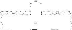
请参考图4至图8,图4至图8为本发明的一优选实施例制作微旋转轴的方法示意图。如图4所示,首先提供一晶片50,例如一硅晶片,并于晶片50的底表面形成一光致抗蚀剂图案52,以定义出一旋转轴区54的位置。如图5所示,接着进行一蚀刻制造工艺,例如一反应性离子蚀刻(reactive ionetching,RIE),利用光致抗蚀剂图案52作为一硬屏蔽,去除位于旋转轴区54的晶片50至一预定深度。其中上述预定深度必须大于后续由晶片50的上表面进行的另一蚀刻制造工艺的变异量与晶片50厚度的变异量的总和,以避免微旋转轴的结构于后续蚀刻制造工艺中损坏。Please refer to FIG. 4 to FIG. 8 . FIG. 4 to FIG. 8 are schematic diagrams of a method for manufacturing a micro-rotating shaft according to a preferred embodiment of the present invention. As shown in FIG. 4 , a
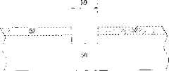
如图6所示,接着去除光致抗蚀剂图案(图未示),并利用一粘着层56将晶片50的底表面接合于一负载载具58上。随后再于晶片50的上表面形成另一光致抗蚀剂图案60,以定义出二穿透区62的位置。其中粘着层56可选用光致抗蚀剂、金属、二氧化硅、苯环丁烯(Benzocyclobutene,BCB)、聚亚酰胺(polyimide)、二氧化硅、金属、胶带、UV胶带或腊等可利用湿蚀刻、加热或照光方式去除的材料。负载载具58则可为硅、玻璃、石英或陶瓷等相容于半导体制造工艺的材料。As shown in FIG. 6 , the photoresist pattern (not shown) is then removed, and an
如图7,接着进行另一蚀刻制造工艺,例如一反应性离子蚀刻制造工艺,利用光致抗蚀剂图案60作为一硬屏蔽,去除位于穿透区62内的晶片50。其中当蚀刻制造工艺进行至图7所示的深度时,位于旋转轴区54的晶片会呈现悬浮状态,而此时蚀刻总面积的最大变化量仅为穿透区62内的晶片面积扣除旋转轴区54内的晶片面积,因此蚀刻总面积并不会产生剧烈变化而使蚀刻制造工艺产生无法预期的变化。除此之外,由于此时尚未蚀刻至粘着层56,因此位于旋转轴区54内的晶片50亦不会产生侧蚀的现象。另外,于本实施例中第一次蚀刻制造工艺中的光致抗蚀剂图案(图未示)所定义出的旋转轴区的尺寸略大于微旋转轴的实际尺寸,藉此可增加第二次蚀刻制造工艺的定位容忍度,藉此后续形成的微旋转轴的形状与尺寸可具有优选的准确性。As shown in FIG. 7 , another etching process, such as a reactive ion etching process, is performed, using the
如图8所示,继续进行蚀刻制造工艺直至蚀穿位于穿透区62内的晶片50为止,并将晶片50上表面的光致抗蚀剂图案60与下表面的粘着层56移除即完成微旋转轴的制作。值得注意的是粘着层56除了粘着晶片50与负载载具58的功能外,亦具有蚀刻停止层的功能,当蚀刻进行至粘着层56时,蚀刻总面积会产生较大的变化,并有可能产生侧蚀现象,然而由于位于旋转轴区54内的晶片50呈悬浮状态,且于第一次蚀刻制造工艺时于旋转轴区54所蚀刻的预定深度即将此次蚀刻制造工艺的变异量与晶片50厚度的变异量考虑在内,因此旋转轴区54内的晶片50不会受到影响。换句话说,微旋转轴的结构不会受到蚀刻制造工艺的变异量的影响,而具有如原先预期的形状,因此具有良好的可靠性。As shown in FIG. 8 , continue the etching process until the
相比于现有技术,本发明的方法利用双面蚀刻方式来制作微旋转轴结构,可有效避免于蚀刻制造工艺中蚀刻总面积变化过大造成蚀刻结果不易控制,以及蚀刻至蚀刻停止层时易发生的侧蚀问题,因此可确保微旋转轴具有良好结构,进而提升微旋转轴的可靠性与可承受的应力。Compared with the prior art, the method of the present invention uses a double-sided etching method to manufacture the micro-rotation shaft structure, which can effectively avoid the difficulty in controlling the etching result due to excessive changes in the total etching area in the etching manufacturing process, and when etching reaches the etching stop layer. The side erosion problem is easy to occur, so it can ensure that the micro-rotation shaft has a good structure, thereby improving the reliability and withstand stress of the micro-rotation shaft.
以上所述仅为本发明的优选实施例,凡依本发明权利要求所做的均等变化与修饰,皆应属本发明专利的涵盖范围。The above descriptions are only preferred embodiments of the present invention, and all equivalent changes and modifications made according to the claims of the present invention shall fall within the scope of the patent of the present invention.
Claims (11)
Priority Applications (1)
| Application Number | Priority Date | Filing Date | Title |
|---|---|---|---|
| CNB200410055871XACN100454144C (en) | 2004-08-05 | 2004-08-05 | Method for double-sided etching of wafers |
Applications Claiming Priority (1)
| Application Number | Priority Date | Filing Date | Title |
|---|---|---|---|
| CNB200410055871XACN100454144C (en) | 2004-08-05 | 2004-08-05 | Method for double-sided etching of wafers |
Publications (2)
| Publication Number | Publication Date |
|---|---|
| CN1731287Atrue CN1731287A (en) | 2006-02-08 |
| CN100454144C CN100454144C (en) | 2009-01-21 |
Family
ID=35963666
Family Applications (1)
| Application Number | Title | Priority Date | Filing Date |
|---|---|---|---|
| CNB200410055871XAExpired - Fee RelatedCN100454144C (en) | 2004-08-05 | 2004-08-05 | Method for double-sided etching of wafers |
Country Status (1)
| Country | Link |
|---|---|
| CN (1) | CN100454144C (en) |
Cited By (1)
| Publication number | Priority date | Publication date | Assignee | Title |
|---|---|---|---|---|
| CN100536259C (en)* | 2006-05-15 | 2009-09-02 | 探微科技股份有限公司 | Method for manufacturing micro connector |
Family Cites Families (4)
| Publication number | Priority date | Publication date | Assignee | Title |
|---|---|---|---|---|
| US6458615B1 (en)* | 1999-09-30 | 2002-10-01 | Carnegie Mellon University | Method of fabricating micromachined structures and devices formed therefrom |
| WO2001053872A1 (en)* | 2000-01-18 | 2001-07-26 | Cornell Research Foundation, Inc. | Single crystal silicon micromirror and array |
| US6818464B2 (en)* | 2001-10-17 | 2004-11-16 | Hymite A/S | Double-sided etching technique for providing a semiconductor structure with through-holes, and a feed-through metalization process for sealing the through-holes |
| SG121844A1 (en)* | 2002-12-20 | 2006-05-26 | Asml Netherlands Bv | Device manufacturing method |
- 2004
- 2004-08-05CNCNB200410055871XApatent/CN100454144C/ennot_activeExpired - Fee Related
Cited By (1)
| Publication number | Priority date | Publication date | Assignee | Title |
|---|---|---|---|---|
| CN100536259C (en)* | 2006-05-15 | 2009-09-02 | 探微科技股份有限公司 | Method for manufacturing micro connector |
Also Published As
| Publication number | Publication date |
|---|---|
| CN100454144C (en) | 2009-01-21 |
Similar Documents
| Publication | Publication Date | Title |
|---|---|---|
| CN105353506B (en) | Vertical comb teeth drives MOEMS micro mirror and preparation method thereof | |
| US7083997B2 (en) | Bonded wafer optical MEMS process | |
| TWI443730B (en) | A progressive trimming method | |
| US6465355B1 (en) | Method of fabricating suspended microstructures | |
| Burger et al. | High-resolution shadow-mask patterning in deep holes and its application to an electrical wafer feed-through | |
| CN103086316B (en) | MEMS vertical comb micro-mirror surface driver manufacturing method | |
| US6752931B2 (en) | Method for using DRIE with reduced lateral etching | |
| JP2002373912A (en) | Integrated circuit and fine working system | |
| JP2007015101A (en) | Hidden hinge mems device | |
| US6587613B2 (en) | Hybrid MEMS fabrication method and new optical MEMS device | |
| JP4688600B2 (en) | Manufacturing method of semiconductor sensor | |
| CN100515921C (en) | Method for producing microstructure and microstructure | |
| CN1731287A (en) | Method for Etching Wafers on Both Sides | |
| CN1247443C (en) | Dry deeply etching silicone wafer manufacture | |
| CN117105167A (en) | A method of manufacturing a MEMS torsion mirror array | |
| TWI255503B (en) | Method of double-sided etching | |
| CN110571130A (en) | Wafer alignment bonding method | |
| TWI606007B (en) | Micro-eletromechanical element using composite substrate and manufacturing method thereof | |
| CN110002395A (en) | Piezoresistive dual-axis motion sensor and method of making the same | |
| CN1792765A (en) | Nano-width resonant structures on silicon-on-insulator wafers and methods of making the same | |
| JPS63175442A (en) | Manufacture of multilayer interconnection type integrated circuit | |
| CN101121498B (en) | How to make a micro torsion shaft | |
| CN112047294B (en) | Infrared MEMS bridge column structure and process method | |
| US6797591B1 (en) | Method for forming a semiconductor device and a semiconductor device formed by the method | |
| GB2387026A (en) | Method of coating contact holes in MEMS and micro-machining applications |
Legal Events
| Date | Code | Title | Description |
|---|---|---|---|
| C06 | Publication | ||
| PB01 | Publication | ||
| C10 | Entry into substantive examination | ||
| SE01 | Entry into force of request for substantive examination | ||
| C14 | Grant of patent or utility model | ||
| GR01 | Patent grant | ||
| CF01 | Termination of patent right due to non-payment of annual fee | Granted publication date:20090121 Termination date:20140805 | |
| EXPY | Termination of patent right or utility model |