CN1725519A - Antiferromagnetic/Ferromagnetic Exchange Coupling Structure Perpendicular Magnetic Bias Abnormal Magnetoresistive Sensor - Google Patents
Antiferromagnetic/Ferromagnetic Exchange Coupling Structure Perpendicular Magnetic Bias Abnormal Magnetoresistive SensorDownload PDFInfo
- Publication number
- CN1725519A CN1725519ACNA2005100814157ACN200510081415ACN1725519ACN 1725519 ACN1725519 ACN 1725519ACN A2005100814157 ACNA2005100814157 ACN A2005100814157ACN 200510081415 ACN200510081415 ACN 200510081415ACN 1725519 ACN1725519 ACN 1725519A
- Authority
- CN
- China
- Prior art keywords
- ferromagnetic layer
- transducer
- active film
- layer
- emr
- Prior art date
- Legal status (The legal status is an assumption and is not a legal conclusion. Google has not performed a legal analysis and makes no representation as to the accuracy of the status listed.)
- Pending
Links
- 230000005291magnetic effectEffects0.000titleclaimsabstractdescription84
- 230000005294ferromagnetic effectEffects0.000titleclaimsabstractdescription67
- 230000005290antiferromagnetic effectEffects0.000titleclaimsabstractdescription38
- 230000008878couplingEffects0.000titleclaimsdescription7
- 238000010168coupling processMethods0.000titleclaimsdescription7
- 238000005859coupling reactionMethods0.000titleclaimsdescription7
- 230000002159abnormal effectEffects0.000titledescription3
- 229910000480nickel oxideInorganic materials0.000claimsabstractdescription5
- GNRSAWUEBMWBQH-UHFFFAOYSA-NoxonickelChemical compound[Ni]=OGNRSAWUEBMWBQH-UHFFFAOYSA-N0.000claimsabstractdescription5
- 229910000428cobalt oxideInorganic materials0.000claimsabstract3
- 239000000463materialSubstances0.000claimsdescription28
- 239000004065semiconductorSubstances0.000claimsdescription25
- 239000000758substrateSubstances0.000claimsdescription16
- 229910052763palladiumInorganic materials0.000claimsdescription13
- 229910052697platinumInorganic materials0.000claimsdescription13
- XEEYBQQBJWHFJM-UHFFFAOYSA-NironSubstances[Fe]XEEYBQQBJWHFJM-UHFFFAOYSA-N0.000claimsdescription12
- 229910052742ironInorganic materials0.000claimsdescription11
- 229910045601alloyInorganic materials0.000claimsdescription9
- 239000000956alloySubstances0.000claimsdescription9
- 238000009792diffusion processMethods0.000claimsdescription9
- 229910052796boronInorganic materials0.000claimsdescription5
- 239000010941cobaltSubstances0.000claimsdescription5
- GUTLYIVDDKVIGB-UHFFFAOYSA-Ncobalt atomChemical compound[Co]GUTLYIVDDKVIGB-UHFFFAOYSA-N0.000claimsdescription5
- 229910052715tantalumInorganic materials0.000claimsdescription5
- 229910052804chromiumInorganic materials0.000claimsdescription4
- 229910017052cobaltInorganic materials0.000claimsdescription4
- 229910000859α-FeInorganic materials0.000claimsdescription4
- 229910020514Co—YInorganic materials0.000claimsdescription3
- 229910000990Ni alloyInorganic materials0.000claimsdescription3
- 229910001260Pt alloyInorganic materials0.000claimsdescription3
- 229910052802copperInorganic materials0.000claimsdescription3
- 239000010949copperSubstances0.000claimsdescription3
- 229910052759nickelInorganic materials0.000claimsdescription3
- PXHVJJICTQNCMI-UHFFFAOYSA-NnickelSubstances[Ni]PXHVJJICTQNCMI-UHFFFAOYSA-N0.000claimsdescription3
- TWNQGVIAIRXVLR-UHFFFAOYSA-Noxo(oxoalumanyloxy)alumaneChemical compoundO=[Al]O[Al]=OTWNQGVIAIRXVLR-UHFFFAOYSA-N0.000claimsdescription3
- 229910052760oxygenInorganic materials0.000claimsdescription3
- 229910052709silverInorganic materials0.000claimsdescription3
- 229910018979CoPtInorganic materials0.000claimsdescription2
- 229910005335FePtInorganic materials0.000claimsdescription2
- 229910052758niobiumInorganic materials0.000claimsdescription2
- BASFCYQUMIYNBI-UHFFFAOYSA-NplatinumSubstances[Pt]BASFCYQUMIYNBI-UHFFFAOYSA-N0.000claims8
- KDLHZDBZIXYQEI-UHFFFAOYSA-NpalladiumSubstances[Pd]KDLHZDBZIXYQEI-UHFFFAOYSA-N0.000claims7
- OQCGPOBCYAOYSD-UHFFFAOYSA-Ncobalt palladiumChemical compound[Co].[Co].[Co].[Pd].[Pd]OQCGPOBCYAOYSD-UHFFFAOYSA-N0.000claims3
- GUBSQCSIIDQXLB-UHFFFAOYSA-Ncobalt platinumChemical compound[Co].[Pt].[Pt].[Pt]GUBSQCSIIDQXLB-UHFFFAOYSA-N0.000claims3
- OBACEDMBGYVZMP-UHFFFAOYSA-Niron platinumChemical compound[Fe].[Fe].[Pt]OBACEDMBGYVZMP-UHFFFAOYSA-N0.000claims3
- 229910052581Si3N4Inorganic materials0.000claims2
- ZGDWHDKHJKZZIQ-UHFFFAOYSA-Ncobalt nickelChemical compound[Co].[Ni].[Ni].[Ni]ZGDWHDKHJKZZIQ-UHFFFAOYSA-N0.000claims2
- 229910052741iridiumInorganic materials0.000claims2
- 238000001556precipitationMethods0.000claims2
- HQVNEWCFYHHQES-UHFFFAOYSA-Nsilicon nitrideChemical compoundN12[Si]34N5[Si]62N3[Si]51N64HQVNEWCFYHHQES-UHFFFAOYSA-N0.000claims2
- 239000010944silver (metal)Substances0.000claims2
- 238000009413insulationMethods0.000claims1
- SORXVYYPMXPIFD-UHFFFAOYSA-Niron palladiumChemical compound[Fe].[Pd]SORXVYYPMXPIFD-UHFFFAOYSA-N0.000claims1
- 229910052703rhodiumInorganic materials0.000claims1
- 239000010948rhodiumSubstances0.000claims1
- 230000004044responseEffects0.000abstractdescription13
- 239000003302ferromagnetic materialSubstances0.000abstractdescription7
- 229910019041PtMnInorganic materials0.000abstractdescription6
- 239000002885antiferromagnetic materialSubstances0.000abstractdescription6
- 229910015136FeMnInorganic materials0.000abstractdescription4
- 229910000914Mn alloyInorganic materials0.000abstractdescription4
- 229910003289NiMnInorganic materials0.000abstractdescription4
- IVMYJDGYRUAWML-UHFFFAOYSA-Ncobalt(ii) oxideChemical compound[Co]=OIVMYJDGYRUAWML-UHFFFAOYSA-N0.000abstractdescription3
- 239000010410layerSubstances0.000description115
- 230000004888barrier functionEffects0.000description6
- 230000005415magnetizationEffects0.000description6
- WPYVAWXEWQSOGY-UHFFFAOYSA-Nindium antimonideChemical compound[Sb]#[In]WPYVAWXEWQSOGY-UHFFFAOYSA-N0.000description5
- XUIMIQQOPSSXEZ-UHFFFAOYSA-NSiliconChemical compound[Si]XUIMIQQOPSSXEZ-UHFFFAOYSA-N0.000description4
- 238000000151depositionMethods0.000description4
- 239000012528membraneSubstances0.000description4
- 229910052751metalInorganic materials0.000description4
- 239000002184metalSubstances0.000description4
- 229910052710siliconInorganic materials0.000description4
- 239000010703siliconSubstances0.000description4
- 230000008021depositionEffects0.000description3
- 239000002346layers by functionSubstances0.000description3
- 238000000034methodMethods0.000description3
- 230000037230mobilityEffects0.000description3
- 239000000126substanceSubstances0.000description3
- 230000007704transitionEffects0.000description3
- 229910018072Al 2 O 3Inorganic materials0.000description2
- JBRZTFJDHDCESZ-UHFFFAOYSA-NAsGaChemical compound[As]#[Ga]JBRZTFJDHDCESZ-UHFFFAOYSA-N0.000description2
- 229910000673Indium arsenideInorganic materials0.000description2
- 229910052782aluminiumInorganic materials0.000description2
- XAGFODPZIPBFFR-UHFFFAOYSA-NaluminiumChemical compound[Al]XAGFODPZIPBFFR-UHFFFAOYSA-N0.000description2
- 238000000137annealingMethods0.000description2
- 230000008901benefitEffects0.000description2
- 230000008859changeEffects0.000description2
- 239000002019doping agentSubstances0.000description2
- RPQDHPTXJYYUPQ-UHFFFAOYSA-Nindium arsenideChemical compound[In]#[As]RPQDHPTXJYYUPQ-UHFFFAOYSA-N0.000description2
- 239000011810insulating materialSubstances0.000description2
- 150000004767nitridesChemical class0.000description2
- 238000001020plasma etchingMethods0.000description2
- 238000012887quadratic functionMethods0.000description2
- 238000000992sputter etchingMethods0.000description2
- 229910000531Co alloyInorganic materials0.000description1
- 229910019222CoCrPtInorganic materials0.000description1
- 229910002546FeCoInorganic materials0.000description1
- 229910001218Gallium arsenideInorganic materials0.000description1
- 229910004298SiO 2Inorganic materials0.000description1
- 230000000903blocking effectEffects0.000description1
- 239000000969carrierSubstances0.000description1
- 238000005229chemical vapour depositionMethods0.000description1
- 238000001816coolingMethods0.000description1
- 238000005260corrosionMethods0.000description1
- 230000007797corrosionEffects0.000description1
- 238000005137deposition processMethods0.000description1
- 239000012777electrically insulating materialSubstances0.000description1
- 230000008020evaporationEffects0.000description1
- 238000001704evaporationMethods0.000description1
- 230000001747exhibiting effectEffects0.000description1
- 230000005621ferroelectricityEffects0.000description1
- -1for exampleInorganic materials0.000description1
- 239000004047hole gasSubstances0.000description1
- 239000012535impuritySubstances0.000description1
- 238000007737ion beam depositionMethods0.000description1
- 238000001451molecular beam epitaxyMethods0.000description1
- NQNBVCBUOCNRFZ-UHFFFAOYSA-Nnickel ferriteChemical compound[Ni]=O.O=[Fe]O[Fe]=ONQNBVCBUOCNRFZ-UHFFFAOYSA-N0.000description1
- 230000009972noncorrosive effectEffects0.000description1
- 230000005298paramagnetic effectEffects0.000description1
- 238000005498polishingMethods0.000description1
- 230000008569processEffects0.000description1
- 239000002356single layerSubstances0.000description1
- 238000004544sputter depositionMethods0.000description1
- 230000005641tunnelingEffects0.000description1
- 230000005533two-dimensional electron gasEffects0.000description1
- 229910052720vanadiumInorganic materials0.000description1
Images


Classifications
- G—PHYSICS
- G11—INFORMATION STORAGE
- G11B—INFORMATION STORAGE BASED ON RELATIVE MOVEMENT BETWEEN RECORD CARRIER AND TRANSDUCER
- G11B5/00—Recording by magnetisation or demagnetisation of a record carrier; Reproducing by magnetic means; Record carriers therefor
- G11B5/127—Structure or manufacture of heads, e.g. inductive
- G11B5/33—Structure or manufacture of flux-sensitive heads, i.e. for reproduction only; Combination of such heads with means for recording or erasing only
- G11B5/39—Structure or manufacture of flux-sensitive heads, i.e. for reproduction only; Combination of such heads with means for recording or erasing only using magneto-resistive devices or effects
- G—PHYSICS
- G11—INFORMATION STORAGE
- G11C—STATIC STORES
- G11C11/00—Digital stores characterised by the use of particular electric or magnetic storage elements; Storage elements therefor
- G11C11/02—Digital stores characterised by the use of particular electric or magnetic storage elements; Storage elements therefor using magnetic elements
- G11C11/14—Digital stores characterised by the use of particular electric or magnetic storage elements; Storage elements therefor using magnetic elements using thin-film elements
- B—PERFORMING OPERATIONS; TRANSPORTING
- B82—NANOTECHNOLOGY
- B82Y—SPECIFIC USES OR APPLICATIONS OF NANOSTRUCTURES; MEASUREMENT OR ANALYSIS OF NANOSTRUCTURES; MANUFACTURE OR TREATMENT OF NANOSTRUCTURES
- B82Y25/00—Nanomagnetism, e.g. magnetoimpedance, anisotropic magnetoresistance, giant magnetoresistance or tunneling magnetoresistance
- G—PHYSICS
- G01—MEASURING; TESTING
- G01R—MEASURING ELECTRIC VARIABLES; MEASURING MAGNETIC VARIABLES
- G01R33/00—Arrangements or instruments for measuring magnetic variables
- G01R33/02—Measuring direction or magnitude of magnetic fields or magnetic flux
- G01R33/06—Measuring direction or magnitude of magnetic fields or magnetic flux using galvano-magnetic devices
- G01R33/09—Magnetoresistive devices
- G01R33/093—Magnetoresistive devices using multilayer structures, e.g. giant magnetoresistance sensors
- G—PHYSICS
- G01—MEASURING; TESTING
- G01R—MEASURING ELECTRIC VARIABLES; MEASURING MAGNETIC VARIABLES
- G01R33/00—Arrangements or instruments for measuring magnetic variables
- G01R33/02—Measuring direction or magnitude of magnetic fields or magnetic flux
- G01R33/06—Measuring direction or magnitude of magnetic fields or magnetic flux using galvano-magnetic devices
- G01R33/09—Magnetoresistive devices
- G01R33/095—Magnetoresistive devices extraordinary magnetoresistance sensors
- G—PHYSICS
- G11—INFORMATION STORAGE
- G11B—INFORMATION STORAGE BASED ON RELATIVE MOVEMENT BETWEEN RECORD CARRIER AND TRANSDUCER
- G11B5/00—Recording by magnetisation or demagnetisation of a record carrier; Reproducing by magnetic means; Record carriers therefor
- G11B5/127—Structure or manufacture of heads, e.g. inductive
- G11B5/33—Structure or manufacture of flux-sensitive heads, i.e. for reproduction only; Combination of such heads with means for recording or erasing only
- G11B5/39—Structure or manufacture of flux-sensitive heads, i.e. for reproduction only; Combination of such heads with means for recording or erasing only using magneto-resistive devices or effects
- G11B5/3903—Structure or manufacture of flux-sensitive heads, i.e. for reproduction only; Combination of such heads with means for recording or erasing only using magneto-resistive devices or effects using magnetic thin film layers or their effects, the films being part of integrated structures
- G11B5/3993—Structure or manufacture of flux-sensitive heads, i.e. for reproduction only; Combination of such heads with means for recording or erasing only using magneto-resistive devices or effects using magnetic thin film layers or their effects, the films being part of integrated structures in semi-conductors
- H—ELECTRICITY
- H10—SEMICONDUCTOR DEVICES; ELECTRIC SOLID-STATE DEVICES NOT OTHERWISE PROVIDED FOR
- H10N—ELECTRIC SOLID-STATE DEVICES NOT OTHERWISE PROVIDED FOR
- H10N50/00—Galvanomagnetic devices
- H10N50/10—Magnetoresistive devices
- G—PHYSICS
- G11—INFORMATION STORAGE
- G11B—INFORMATION STORAGE BASED ON RELATIVE MOVEMENT BETWEEN RECORD CARRIER AND TRANSDUCER
- G11B5/00—Recording by magnetisation or demagnetisation of a record carrier; Reproducing by magnetic means; Record carriers therefor
- G11B2005/0002—Special dispositions or recording techniques
- G11B2005/0005—Arrangements, methods or circuits
- G11B2005/0008—Magnetic conditionning of heads, e.g. biasing
Landscapes
- Engineering & Computer Science (AREA)
- Physics & Mathematics (AREA)
- Manufacturing & Machinery (AREA)
- Chemical & Material Sciences (AREA)
- Nanotechnology (AREA)
- Condensed Matter Physics & Semiconductors (AREA)
- General Physics & Mathematics (AREA)
- Crystallography & Structural Chemistry (AREA)
- Computer Hardware Design (AREA)
- Hall/Mr Elements (AREA)
- Magnetic Heads (AREA)
- Thin Magnetic Films (AREA)
Abstract
Description
Translated fromChinese技术领域technical field
本发明涉及磁电阻(magnetoresistive)传感器,更特别地涉及一种基于异常磁电阻(EMR)的传感器。The present invention relates to magnetoresistive sensors, and more particularly to a sensor based on abnormal magnetoresistance (EMR).
背景技术Background technique
基于异常磁电阻(EMR)的磁电阻传感器已经被建议作为用于磁记录硬盘驱动器的读取头(read-head)传感器。因为EMR传感器中的有源区是由非磁性半导体材料形成的,EMR传感器不会遇到磁噪声的问题,所述磁噪声问题存在于基于巨磁电阻(GMR)和隧道磁电阻(tunneling magnetoresistance:TMR)的读取头传感器中,这两种传感器在它们的有源区中都使用了磁性膜。Magnetoresistance sensors based on abnormal magnetoresistance (EMR) have been proposed as read-head sensors for magnetic recording hard disk drives. Because the active region in an EMR sensor is formed from a non-magnetic semiconductor material, the EMR sensor does not suffer from the problems of magnetic noise that exist based on giant magnetoresistance (GMR) and tunneling magnetoresistance: TMR) read head sensors, both of which use magnetic films in their active regions.
EMR包括与有源区的一侧接触的一对电压引线和一对电流引线、以及与有源区的另一侧接触的导电分路。没有施加磁场时,经过电流引线的传感电流(sense current)进入半导体有源区并经过分路而分流。当存在施加的磁场时,电流从分路偏离,主要流过半导体有源区。通过电压引线检测施加的磁场导致的电阻变化。T.Zhou等人发表在应用物理快报(Appl.Phys.Lett.)2001年1月29日第78卷第5期第667-669页的文章“Extraordinarymagnetoresistance in externallY shunted van der Pauw plates”中描述了EMR。S.A.Solin等人发表在应用物理快报(Appl.Phys.Lett.)2002年5月27日第80卷第21期第4012-4014页的文章“Nonmagnetic semiconductors asread-head sensors for ultra-high-density magnetic recording”中说明了用于读取头应用的EMR传感器。The EMR includes a pair of voltage leads and a pair of current leads contacting one side of the active region, and a conductive shunt contacting the other side of the active region. When no magnetic field is applied, the sense current through the current lead enters the semiconductor active region and is shunted through the shunt. When there is an applied magnetic field, the current diverges from the shunt and flows primarily through the semiconductor active region. The change in resistance caused by an applied magnetic field is detected through the voltage leads. Described in the article "Extraordinary magnetoresistance in externalY shuttered van der Pauw plates" published by T.Zhou et al. EMR. S.A.Solin et al published the article "Nonmagnetic semiconductors asread-head sensors for ultra-high-density magnetic recording" describes EMR sensors for readhead applications.
EMR传感器的问题之一是它的磁电阻近似为施加的磁场的二次函数。因此在来自所记录的磁介质的小磁场面前,磁电阻响应较小而且是非线性的。有人建议通过电压引线的位置不对称来实现EMR传感器的偏置。也有人建议通过使用单铁磁层对传感器施加垂直磁场来实现EMR传感器的偏置,如美国专利6,714,374中所说明的。One of the problems with EMR sensors is that their magnetoresistance is approximately a quadratic function of the applied magnetic field. The magnetoresistance response is therefore small and non-linear in the presence of small magnetic fields from the recorded magnetic medium. It has been suggested to achieve biasing of the EMR sensor by asymmetrical placement of the voltage leads. It has also been proposed to bias an EMR sensor by applying a perpendicular magnetic field to the sensor using a single ferromagnetic layer, as described in US Patent 6,714,374.
需要具有改进的磁场偏置的EMR传感器,使得在施加的小的磁场中传感器具有更高的磁电阻并且对施加的磁场的有更线性的响应。There is a need for EMR sensors with improved magnetic field biasing such that the sensor has higher magnetoresistance at small applied magnetic fields and a more linear response to the applied magnetic field.
发明内容Contents of the invention
本发明是一种EMR传感器,其使用反铁磁/铁磁交换耦合双层结构来为传感器提供垂直磁偏置。双层结构中的铁磁层具有垂直磁各向异性并被反铁磁层交换偏置。反铁磁/铁磁双层结构位于EMR有源膜的顶部,并提供垂直于有源膜平面的磁场来偏置EMR传感器的磁电阻对磁场的响应。The present invention is an EMR sensor that uses an antiferromagnetic/ferromagnetic exchange coupled bilayer structure to provide a vertical magnetic bias for the sensor. The ferromagnetic layer in the bilayer structure has perpendicular magnetic anisotropy and is exchange-biased by the antiferromagnetic layer. The antiferromagnetic/ferromagnetic bilayer structure sits on top of the EMR active film and provides a magnetic field perpendicular to the plane of the active film to bias the magnetoresistance response of the EMR sensor to the magnetic field.
铁磁层可由能够以其磁化方向可基本垂直于层平面而定向的方式来制备的铁磁材料或多层形成。可通过选择具有内在实质上离面(out-of-plane)的磁各向异性的铁磁材料来实现磁化基本垂直于平面。反铁磁层可由任何已知的锰合金形成,例如PtMn、NiMn、FeMn、IrMn、PdMn、PtPdMn和RhMn,或由任何绝缘反铁磁材料形成,例如那些基于钴氧化物和镍氧化物的反铁磁材料。双层结构中铁磁层或者反铁磁层可以是下层。扩散阻挡层(diffusionbarrier)可位于EMR有源膜和反铁磁/铁磁交换耦合双层之间。The ferromagnetic layer may be formed from a ferromagnetic material or layers that can be prepared in such a way that the direction of its magnetization can be oriented substantially perpendicular to the plane of the layer. Magnetization substantially perpendicular to the plane can be achieved by selecting a ferromagnetic material with inherent magnetic anisotropy substantially out-of-plane. The antiferromagnetic layer can be formed from any known manganese alloys, such as PtMn, NiMn, FeMn, IrMn, PdMn, PtPdMn, and RhMn, or from any insulating antiferromagnetic material, such as those based on cobalt oxides and nickel oxides. ferromagnetic material. A ferromagnetic layer or an antiferromagnetic layer may be the lower layer in the bilayer structure. A diffusion barrier may be located between the EMR active film and the antiferromagnetic/ferromagnetic exchange coupled bilayer.
为了更全面地理解本发明的本质和优点,应该参考下面结合附图的详细描述。For a fuller understanding of the nature and advantages of the present invention, reference should be made to the following detailed description taken in conjunction with the accompanying drawings.
附图说明Description of drawings
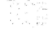
图1是现有技术EMR传感器的立体图。FIG. 1 is a perspective view of a prior art EMR sensor.
图2是图1的现有技术EMR传感器通过EMR有源膜截面的俯视示意图,示出该传感器的基本操作。FIG. 2 is a schematic top view of the prior art EMR sensor of FIG. 1 in section through the EMR active membrane, illustrating the basic operation of the sensor.
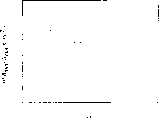
图3A是具有对称电流和电压引线的现有技术EMR传感器的理论上的磁电阻对磁场的响应。Figure 3A is the theoretical magnetoresistance response to magnetic field of a prior art EMR sensor with symmetrical current and voltage leads.
图3B是具有不对称电流和电压引线的现有技术EMR传感器的理论上的磁电阻对磁场的响应。Figure 3B is the theoretical magnetoresistance response to magnetic field of a prior art EMR sensor with asymmetric current and voltage leads.
图4是依照本发明的EMR传感器的立体图。Figure 4 is a perspective view of an EMR sensor in accordance with the present invention.
具体实施方式Detailed ways
<现有技术><Prior Art>
图1是现有技术EMR传感器10的立体图。EMR传感器10包括形成在半导体衬底12例如GaAs上的III-V异质结构20。但是,本发明中所述的EMR传感器并不局限于III-V半导体材料。例如,它也可以形成在硅的基础上。异质结构20包括具有第一带隙(band-gap)的半导体材料的第一层22、形成在第一层22顶部并具有比第一带隙更小的第二带隙的半导体材料的第二层30、以及形成在第二层30顶部并具有比第二带隙更大的第三带隙的半导体材料的第三层24。第一和第三层22、24中的材料可以相似或者相同。第一、第二和第三半导体材料层因其不同材料的不同带隙而产生能量势阱(量子阱)。因此载流子被限制在层30中,层30被视为传感器10中的EMR有源膜。FIG. 1 is a perspective view of a prior
通常第一层22形成在缓冲层26上面,缓冲层26可以是一层或更多层。缓冲层26包括数个周期的超晶格(superlattice)结构,用来防止衬底中存在的杂质迁移到功能层(functional layer)22、24和30中。另外,缓冲层26选择为适应衬底12和异质结构20的功能层的通常不同的晶格常数,因此在衬底和功能层之间起到应力释放层的作用。Typically first layer 22 is formed over buffer layer 26, which may be one or more layers. The buffer layer 26 includes several periods of a superlattice structure for preventing impurities present in the substrate from migrating into the
一个或更多掺杂层被结合进第一层22、第三层24、或者22和24两层的半导体材料中,并且与第二和第三半导体材料的边界分离开。掺杂层为量子阱提供电子(如果n掺杂)或空穴(如果p掺杂)。电子或空穴分别以二维电子气或空穴气(hole-gas)的形式聚集在量子阱中。One or more doped layers are incorporated into the semiconductor material of the first layer 22, the third layer 24, or both layers 22 and 24, and are separated from the boundaries of the second and third semiconductor materials. The doped layer provides electrons (if n-doped) or holes (if p-doped) to the quantum well. Electrons or holes accumulate in the quantum well in the form of two-dimensional electron gas or hole-gas, respectively.
如前面引用的参考文献所描述的,层22/30/24可以是生长在半绝缘砷化镓(GaAs)衬底12上的Al0.09In0.91Sb/InSb/Al0.09In0.91Sb异质结构,在该异质结构和衬底之间具有缓冲层26。InSb是窄带隙半导体。窄带隙半导体通常表现出具有较高的电子迁移率,因为其有效电子质量(electron mass)被大大减小。典型的窄带隙材料是InSb和InAs。例如,InSb和InAs的室温电子迁移率分别是70,000cm2/Vs和35,000cm2/Vs。Layers 22/30/24 may be Al0.09 In0.91 Sb/InSb/Al0.09 In0.91 Sb heterostructures grown on semi-insulating gallium arsenide (GaAs)
形成在缓冲层26上的底Al0.09In0.91Sb层22的厚度在大约1-3微米的范围,并且顶Al0.09In0.91Sb层24的厚度在大约10到1000nm的范围,通常为50nm。结合进层22或24之中的掺杂层的厚度从一个单层(monolayer)(delta-doped layer:σ掺杂层)到10nm。掺杂层与第一和第二或第二和第三半导体材料的InSb/Al0.09In0.91Sb边界间隔10-300的距离。因为通常电子比空穴具有更高的迁移率,因此N型掺杂是优选的。通常N型掺杂剂是浓度范围为1-1019/cm3的硅。异质结构20的沉积工艺优选为分子束外延,但是也可使用其他外延生长方法。The bottom Al0.09 In0.91 Sb layer 22 formed on the buffer layer 26 has a thickness in the range of about 1-3 microns, and the top Al0.09 In0.91 Sb layer 24 has a thickness in the range of about 10 to 1000 nm, typically 50 nm. The thickness of the doped layer incorporated into layer 22 or 24 is from a monolayer (delta-doped layer: σ-doped layer) to 10 nm. The doped layer is spaced at a distance of 10-300 Å from the InSb/Al0.09 In0.91 Sb boundary of the first and second or second and third semiconductor materials. N-type doping is preferred because electrons generally have a higher mobility than holes. Typically the N-type dopant is silicon in a concentration range of 1-1019 /cm3 . The deposition process of the heterostructure 20 is preferably molecular beam epitaxy, but other epitaxial growth methods may also be used.
在异质结构20上形成盖层(capping layer)40来防止器件被腐蚀。盖层可以由绝缘材料例如铝或硅的氧化物或氮化物(例如Si3N4,Al2O3)或由非腐蚀性半绝缘半导体形成。A capping layer 40 is formed on the heterostructure 20 to prevent the device from being corroded. The capping layer may be formed from an insulating material such as an oxide or nitride of aluminum or silicon (eg Si3 N4 , Al2 O3 ) or from a non-corrosive semi-insulating semiconductor.
在EMR结构20的一侧上构图两个电流引线50,52和两个电压引线60,62,使得它们与量子阱电接触。在EMR结构20的对着电流和电压引线的侧面上构图金属分路70,使得其与量子阱电接触。箭头示出施加的磁场也就是将被感测的磁场,其与EMR结构20中的膜平面正交。引线通常包括金属接触,例如扩散到器件中的Au、AuGe或Ge。通常在形成盖层40后形成引线,有时候在除去一些盖层材料之后。Two current leads 50, 52 and two voltage leads 60, 62 are patterned on one side of the EMR structure 20 such that they are in electrical contact with the quantum wells. Metal shunts 70 are patterned on the side of the EMR structure 20 facing the current and voltage leads so that they make electrical contact with the quantum wells. Arrows show the applied magnetic field, ie the magnetic field to be sensed, which is normal to the membrane plane in the EMR structure 20 . Leads typically include metal contacts such as Au, AuGe or Ge diffused into the device. Leads are typically formed after capping layer 40 is formed, and sometimes after some capping material is removed.
图2是EMR传感器通过有源膜30截面的俯视示意图,说明了传感器的基本运行方式。在没有施加的磁场H时,通过引线50、52的传感电流进入半导体有源膜30并通过分路70被分流,如线80所示。当存在施加的磁场H时,如图2中的箭尾所示进入页面,电流从分路70偏移,主要经过半导体有源膜30,如线条82所示。通过电压引线60、62探测到施加的磁场导致的电阻变化。FIG. 2 is a schematic top view of a cross-section of the EMR sensor through the
现有技术EMR传感器10的问题之一是它的磁电阻[(R-Rmin)/Rmin]近似为施加的磁场的二次函数。因此,对于所关心的范围内的施加的磁场,也就是来自记录的磁介质的小磁场,磁电阻响应小并且是非线性的。图3A中具有对称电流和电压引线的EMR传感器的理论的磁电阻对磁场的响应示出了这一点,该EMR传感器和图1-2以及和图3A里的插图所示出的一样。One of the problems with the prior
有人建议通过电压引线位置不对称来实现EMR传感器的偏置,如图3B中插图所示。图3B示出包括不对称电压引线的EMR传感器的理论的磁电阻对磁场的响应。在施加的磁场为零时图3B中的传感器比图3A中的传感器具有更高的磁电阻和更线性的响应。It has been proposed to bias the EMR sensor by asymmetrically positioning the voltage leads, as shown in the inset of Figure 3B. Figure 3B shows the theoretical magnetoresistance response to magnetic field for an EMR sensor including asymmetric voltage leads. The sensor in Figure 3B has a higher magnetoresistance and a more linear response than the sensor in Figure 3A at zero applied magnetic field.
也有人建议通过使用单铁磁层对传感器施加一垂直磁场来实现EMR传感器的偏置,如美国专利6,714,374中所说明的。It has also been proposed to bias an EMR sensor by applying a perpendicular magnetic field to the sensor using a single ferromagnetic layer, as described in US Patent 6,714,374.
<本发明><this invention>
本发明的EMR传感器包含铁磁材料层,其利用反铁磁层被垂直于层的平面地交换偏置并且位于EMR膜结构之上。该反铁磁/铁磁(AF/F)双层结构提供偏置EMR传感器的磁电阻对磁场响应的磁场。美国专利6,650,513中说明了AF/F结构中具有矫顽力增强和磁滞回线位移(hysteresis loop-shift)的垂直于平面的交换偏置(exchange-biasing),对于该AF/F结构,铁磁层具有离面(out-of-plane)的铁磁性易轴(easy axis)。垂直交换偏置的大小和在类似的AF/F结构中发现的相当,对于该类似的AF/F结构,铁磁层在层的平面内被交换偏置。The EMR sensor of the present invention comprises a layer of ferromagnetic material that is exchange biased perpendicular to the plane of the layer with an antiferromagnetic layer and is located above the EMR membrane structure. The antiferromagnetic/ferromagnetic (AF/F) bilayer structure provides a magnetic field that biases the magnetoresistive response of the EMR sensor to a magnetic field. Perpendicular to plane exchange-biasing with coercivity enhancement and hysteresis loop-shift in an AF/F structure is described in U.S. Patent 6,650,513. For this AF/F structure, iron The magnetosphere has an out-of-plane ferromagnetic easy axis. The magnitude of the vertical exchange bias is comparable to that found in similar AF/F structures for which the ferromagnetic layer is exchange biased in the plane of the layer.
图4是根据本发明的EMR传感器的立体图。该EMR传感器110和现有技术传感器10相似处在于,具有形成在半导体衬底112上的量子阱膜结构120,该量子阱膜结构120包括第一半导体层122、第二半导体且EMR有源层130和第三半导体层124以及缓冲层126。两个电流引线150、152和两个电压引线160、162与EMR有源膜130电接触并且金属分路170与EMR有源膜130在对着电流和电压引线的侧上电接触。箭头示出施加的磁场H,也就是将要被感测的磁场,并且该磁场垂直于EMR结构120中膜的平面。盖层140在传感器110之上。Fig. 4 is a perspective view of an EMR sensor according to the present invention. The
EMR传感器110也包括衬底120上的铁磁层180。图4所示的优选实施例中EMR结构120位于衬底112和铁磁层180之间。铁磁层180具有垂直磁各向异性和垂直于EMR有源膜130的平面定向的垂直平面(out-of-plane)磁矩181。源自铁磁层180的磁矩181是偏置磁场,EMR有源膜130暴露于该偏置磁场。这使磁电阻对磁场的响应曲线平移,使得在零施加的磁场时传感器110具有更高的磁电阻和更线性的响应。提供偏置磁场的铁磁层180被反铁磁层190交换偏置。
垂直于其平面而磁化的铁磁层所产生的磁场H可以用厚度为t,长度为L的均匀磁化的正方块(square block)的磁场来近似。如果起点(origin)在正方块的上表面,磁场H沿着垂直于层的Y轴方向表示为The magnetic field H generated by a ferromagnetic layer magnetized perpendicular to its plane can be approximated by the magnetic field of a uniformly magnetized square block of thickness t and length L. If the origin is on the upper surface of the square, the magnetic field H is expressed along the Y axis perpendicular to the layer as
并且y是沿着Y轴的距离。作为例子,对于垂直于其平面磁化、磁化强度MS约为1400emu/cm3、长度L=100nm、厚度t=10nm的Co层,在y=10nm处磁场H大约为1400Oe。and y is the distance along the Y axis. As an example, for a Co layer magnetized perpendicular to its plane with a magnetization MS of about 1400 emu/cm3 , a length L=100 nm, and a thickness t=10 nm, the magnetic field H at y=10 nm is about 1400 Oe.
用于铁磁偏置层180的材料可以是任何可用于垂直磁记录的铁磁材料,包括FePt、化学有序L10相的CoPt或(FeCo)Pt合金、CoCrPt合金以及Co/Pd、Co/Pt、Fe/Pd和Fe/Pt多层。以各向异性轴显著垂直于平面(out-of-plane)的方式制备铁磁层,使得它被视为具有“垂直”磁各向异性。这些合金和多层也可以用另外的元素掺杂。例如,CoCrPtX合金被建议用于垂直记录,其中X=B、Nb和Ta是常见的掺杂剂。类似的,Co/Pd和Co/Pt多层中的Co层通常包括元素Y,使得Co是Co-Y合金,其中Y=B、Ta、Cr、O、Cu、Ag、Pt、Pd。其它合适的铁磁材料是铁氧体,例如钴铁氧体或镍铁氧体。这些铁氧体的优点是他们是绝缘的,因此不需要使用绝缘层来分隔EMR异质结构和铁磁偏置层180。The material for the
反铁磁层190可以是充分厚的Mn合金层(PtMn、NiMn、FeMn、IrMn、PdMn、PtPdMn或RhMn)。PtMn层要厚于约100从而在退火后成为化学有序和反铁磁的,而当IrMn层厚于约40时则它沉积时就是反铁磁性的。这些反铁磁Mn合金也可包括少量附加元素,例如Cr、V、Pt、Pd和Ni,通常增加它们用来提高抗腐蚀性或增加电阻。因为这些反铁磁材料是金属的,由诸如由钴氧化物、镍氧化物以及钴和镍合金的氧化物形成的已知的反铁磁材料的电绝缘材料形成反铁磁层190会是所希望的。The
铁磁层180具有本征矫顽力HC0。当它和反铁磁层190交换耦合,它的矫顽力增强到HC>HC0,并且它的M-H回线将被交换场HE平移。根据下式,交换场HE由铁磁层180和反铁磁层190之间的磁耦合强度JA、以及铁磁层180的厚度tF和磁化强度MF决定:The
HE=JA/MFtF。HE =JA /MF tF .
因此,当EMR传感器110意图用于磁记录读取头时,值(HE+HC)必须比来自磁介质上的磁转变(magnetic transition)的磁场即通常在+/-200到+/-500Oe范围的感测磁场大,但低于翻转磁介质的位(bits)所需要的磁场。比来自磁转变的磁场大的(HE+HC)值保证当暴露于施加的磁场时,铁磁层180的磁矩181不翻转(switch)。因此,由于可较大的交换偏置场HE,铁磁层180的本征矫顽力HC0能相对较低。这允许铁磁层180的材料和厚度的选择范围更宽。例如,使用[Co(0.7nm)/Pt(0.5nm)]3多层作为铁磁层180,并用15nm厚PtMn层作为反铁磁层190,产生大约200Oe的HE和大约450Oe的HC。[Co(0.7nm)/Pt(0.5nm)]3多层具有大约100Oe的相对较低的本征矫顽力HC0,这甚至比感测场(sensing field)还低。Therefore, when the
上面例子中的[Co(0.7nm)/Pt(0.5nm)]3多层是表现出本征的垂直于平面的磁各向异性的Co/Pt、Co/Pd、Fe/Pt以及Fe/Pd的组中的一种。这些多层在本发明中特别有用,因为它们可以在较宽范围的矫顽力和有效磁化强度内制备,甚至当在室温或低温沉积时。这些多层的高可调性(tunability)归因于Co和Fe的大磁矩及Pt或Pd的小的多的感生磁矩(induced moment),以及Fe或Co层通过Pt或Pd的高铁磁性耦合(ferromagnetic coupling)。另外,这些多层的M-H回线有高矩形度(high squareness),也就是,剩磁对饱和磁矩的比值接近为1。The [Co(0.7nm)/Pt(0.5nm)]3 multilayers in the above example are Co/Pt, Co/Pd, Fe/Pt, and Fe/Pd exhibiting intrinsic perpendicular-to-plane magnetic anisotropy one of the groups. These multilayers are particularly useful in the present invention because they can be prepared over a wide range of coercivity and effective magnetization, even when deposited at room temperature or low temperature. The high tunability of these multilayers is attributed to the large magnetic moments of Co and Fe and the much smaller induced moments of Pt or Pd, as well as the high ferroelectricity of Fe or Co layers through Pt or Pd. Magnetic coupling (ferromagnetic coupling). In addition, the MH loops of these layers have high squareness, that is, the ratio of remanence to saturation magnetic moment is close to 1.
EMR传感器10可以作为一种选择在EMR结构120和铁磁层180之间包括扩散阻挡层(diffusion barrier)182。用于扩散阻挡层182的合适材料包括铝和硅的氧化物和氮化物,例如,Al2O3、SiO2和Si3N4。
图4中,反铁磁/铁磁双层180/190被描述为反铁磁层190在铁磁层180的上面。但是,反铁磁层190也可位于铁磁层180的下面。这种排列中如果反铁磁层190是电绝缘的,可不需要扩散阻挡层182。In FIG. 4 , antiferromagnetic/
以下面的方式制造EMR传感器110。在半绝缘衬底上生长如前所述的异质结构。通过反应离子刻蚀或离子研磨来刻蚀出定义所要制造的EMR传感器的形状的平台(mesa)。然后例如通过使用例如金属圆点掩模(shadowmask)来沉积引线150、152、160、162和分路170。接着,在平台、引线和分路上沉积绝缘材料例如氧化铝来作为扩散阻挡层182。然后平坦化该结构,例如通过化学机械抛光(CMP)。通过溅射、离子束沉积、蒸镀、分子化学气相沉积(MOCVD)或这些工艺的组合,在平坦化了的表面上沉积铁磁层180和反铁磁层190。然后通过RIE或离子研磨部分地除去铁磁层180和反铁磁层190,使得只有这些层的直接在EMR平台结构之上的、特别是在EMR有源区之上的部分保留下来。如果层190使用如PtMn或NiMn的化学有序反铁磁物质,那么将该结构在方向垂直于层平面的磁场中退火。合金化学地有序化并经历顺磁到反铁磁的相变。冷却到低于反铁磁物质的阻挡温度(blocking temperature)后,也就是铁磁层180和反铁磁层190之间产生交换耦合的温度,反铁磁层190设置并固定位铁磁层180的磁化方向181。另一选择是在更高温度下沉积铁磁层180和反铁磁层190,使得在沉积期间已经诱导反铁磁层190中的化学有序。然后在方向垂直于层平面的磁场中将该结构从沉积温度冷却经过阻挡温度。如果层190使用如IrMn或FeMn的化学无序的反铁磁物质,那么就不需要退火。在方向垂直于层平面的磁场中沉积铁磁层180和反铁磁层190就完全足够了。然而,沉积后在方向垂直于层平面的磁场中的沉积后(post-deposition)退火会是可取的,因为这可以增加偏置场HE。The
尽管已经参考优选实施例特别地示出并说明了本发明,本领域技术人员应理解,在不偏离本发明的思想和范围的情况下,可以进行各种形式和细节上的变化。因此,这里所公开的发明应视为说明性的并限制在所附权利要求所限定的范围。Although the present invention has been particularly shown and described with reference to preferred embodiments, it will be understood by those skilled in the art that various changes in form and details may be made without departing from the spirit and scope of the invention. Accordingly, the invention disclosed herein is to be considered as illustrative and limited in scope as defined in the appended claims.
Claims (22)
Applications Claiming Priority (2)
| Application Number | Priority Date | Filing Date | Title |
|---|---|---|---|
| US10/883,204 | 2004-06-30 | ||
| US10/883,204US7167346B2 (en) | 2004-06-30 | 2004-06-30 | Extraordinary magnetoresistance sensor with perpendicular magnetic biasing by an antiferromagnetic/ferromagnetic exchange-coupled structure |
Publications (1)
| Publication Number | Publication Date |
|---|---|
| CN1725519Atrue CN1725519A (en) | 2006-01-25 |
Family
ID=35464048
Family Applications (1)
| Application Number | Title | Priority Date | Filing Date |
|---|---|---|---|
| CNA2005100814157APendingCN1725519A (en) | 2004-06-30 | 2005-06-30 | Antiferromagnetic/Ferromagnetic Exchange Coupling Structure Perpendicular Magnetic Bias Abnormal Magnetoresistive Sensor |
Country Status (6)
| Country | Link |
|---|---|
| US (1) | US7167346B2 (en) |
| EP (1) | EP1612775A3 (en) |
| KR (1) | KR20060048611A (en) |
| CN (1) | CN1725519A (en) |
| SG (1) | SG118382A1 (en) |
| TW (1) | TW200608041A (en) |
Cited By (5)
| Publication number | Priority date | Publication date | Assignee | Title |
|---|---|---|---|---|
| CN102097101A (en)* | 2009-12-09 | 2011-06-15 | 西部数据(弗里蒙特)公司 | Method and system for providing a magnetic transducer having an improved read sensor |
| CN102568743A (en)* | 2010-12-09 | 2012-07-11 | 中国科学院物理研究所 | Vertical magnetic anisotropy film and preparation method thereof |
| CN103424131A (en)* | 2013-08-26 | 2013-12-04 | 电子科技大学 | Method for preparing perpendicular bias magnetic sensing unit |
| CN108292700A (en)* | 2015-12-07 | 2018-07-17 | 英特尔公司 | The heat budget of magnetic tunnel junction enhances |
| CN114388689A (en)* | 2020-10-20 | 2022-04-22 | 中国科学院物理研究所 | Magneonic Crystal-Based Spin-Wave Switches and Filters |
Families Citing this family (11)
| Publication number | Priority date | Publication date | Assignee | Title |
|---|---|---|---|---|
| US7295406B2 (en)* | 2004-07-22 | 2007-11-13 | Hitachi Global Storage Technologies Netherlands B.V. | Narrow track extraordinary magneto resistive [EMR] device |
| US7564656B2 (en)* | 2005-02-28 | 2009-07-21 | Hitachi Global Storage Technologies Netherlands B.V. | Integrated servo and read EMR sensor |
| US7633718B2 (en)* | 2005-06-27 | 2009-12-15 | Hitachi Global Storage Technologies Netherlands, B.V. | Lead contact structure for EMR elements |
| US7738217B2 (en)* | 2006-02-13 | 2010-06-15 | Hitachi Global Storage Technologies Netherlands B.V. | EMR magnetic head having a magnetic flux guide and a body formed at a tail end of a slider |
| US7466521B2 (en)* | 2006-04-25 | 2008-12-16 | Hitachi Global Storage Technologies Netherlands B.V. | EMR structure with bias control and enhanced linearity of signal |
| DE602006013106D1 (en)* | 2006-06-13 | 2010-05-06 | Hitachi Ltd | Magnetoresistance device |
| US7502206B2 (en)* | 2006-07-24 | 2009-03-10 | Hitachi Global Storage Technologies Netherlands B.V. | Multiple extraordinary magnetoresistive (EMR) sensor utilizing both current leads |
| FR2910716B1 (en)* | 2006-12-26 | 2010-03-26 | Commissariat Energie Atomique | MULTILAYER MAGNETIC DEVICE, METHOD FOR PRODUCING THE SAME, MAGNETIC FIELD SENSOR, MAGNETIC MEMORY AND LOGIC HOLDER USING SUCH A DEVICE |
| US20090218563A1 (en)* | 2008-02-28 | 2009-09-03 | Bruce Alvin Gurney | Novel fabrication of semiconductor quantum well heterostructure devices |
| US8189302B2 (en)* | 2010-09-11 | 2012-05-29 | Hitachi Global Storage Technologies Netherlands B.V. | Magnetic field sensor with graphene sense layer and ferromagnetic biasing layer below the sense layer |
| US20150263267A1 (en)* | 2014-03-13 | 2015-09-17 | Hiroyuki Kanaya | Magnetic memory and method for manufacturing the same |
Family Cites Families (8)
| Publication number | Priority date | Publication date | Assignee | Title |
|---|---|---|---|---|
| US5965283A (en) | 1997-12-23 | 1999-10-12 | Nec Research Institute, Inc. | GMR enhancement in inhomogeneous semiconductors for use in magnetoresistance sensors |
| US6707122B1 (en)* | 1999-11-30 | 2004-03-16 | Nec Laboratories America, Inc. | Extraordinary magnetoresistance at room temperature in inhomogeneous narrow-gap semiconductors |
| US6353317B1 (en) | 2000-01-19 | 2002-03-05 | Imperial College Of Science, Technology And Medicine | Mesoscopic non-magnetic semiconductor magnetoresistive sensors fabricated with island lithography |
| US6714374B1 (en) | 2000-08-31 | 2004-03-30 | Nec Corporation | Magnetoresistive sensor, magnetoresistive head, and magnetic recording/reproducing apparatus |
| US6650513B2 (en) | 2001-01-29 | 2003-11-18 | International Business Machines Corporation | Magnetic devices with a ferromagnetic layer having perpendicular magnetic anisotropy and an antiferromagnetic layer for perpendicularly exchange biasing the ferromagnetic layer |
| US6639760B2 (en) | 2002-01-07 | 2003-10-28 | International Business Machines Corporation | Compliant worm gear and worm gear bracket |
| US6930862B2 (en)* | 2002-01-07 | 2005-08-16 | Hitachi Global Storage Technologies Netherlands B.V. | Shielded extraordinary magnetoresistance head |
| US20040218309A1 (en)* | 2003-04-29 | 2004-11-04 | Seagate Technology Llc | Magnetic read head sensors having geometrical magnetoresistance and disc drives including the sensors |
- 2004
- 2004-06-30USUS10/883,204patent/US7167346B2/ennot_activeExpired - Fee Related
- 2005
- 2005-05-04EPEP05252747Apatent/EP1612775A3/ennot_activeWithdrawn
- 2005-05-26TWTW094117288Apatent/TW200608041A/enunknown
- 2005-06-16SGSG200503879Apatent/SG118382A1/enunknown
- 2005-06-28KRKR1020050056234Apatent/KR20060048611A/ennot_activeWithdrawn
- 2005-06-30CNCNA2005100814157Apatent/CN1725519A/enactivePending
Cited By (8)
| Publication number | Priority date | Publication date | Assignee | Title |
|---|---|---|---|---|
| CN102097101A (en)* | 2009-12-09 | 2011-06-15 | 西部数据(弗里蒙特)公司 | Method and system for providing a magnetic transducer having an improved read sensor |
| CN102097101B (en)* | 2009-12-09 | 2014-08-13 | 西部数据(弗里蒙特)公司 | Method and system for providing a magnetic transducer having an improved read sensor |
| CN102568743A (en)* | 2010-12-09 | 2012-07-11 | 中国科学院物理研究所 | Vertical magnetic anisotropy film and preparation method thereof |
| CN103424131A (en)* | 2013-08-26 | 2013-12-04 | 电子科技大学 | Method for preparing perpendicular bias magnetic sensing unit |
| CN103424131B (en)* | 2013-08-26 | 2015-08-05 | 电子科技大学 | A kind of preparation method of vertical off setting magnetic sensing unit |
| CN108292700A (en)* | 2015-12-07 | 2018-07-17 | 英特尔公司 | The heat budget of magnetic tunnel junction enhances |
| CN108292700B (en)* | 2015-12-07 | 2022-06-07 | 英特尔公司 | Thermal budget enhancement of magnetic tunnel junctions |
| CN114388689A (en)* | 2020-10-20 | 2022-04-22 | 中国科学院物理研究所 | Magneonic Crystal-Based Spin-Wave Switches and Filters |
Also Published As
| Publication number | Publication date |
|---|---|
| US20060002030A1 (en) | 2006-01-05 |
| EP1612775A2 (en) | 2006-01-04 |
| EP1612775A3 (en) | 2007-01-24 |
| TW200608041A (en) | 2006-03-01 |
| SG118382A1 (en) | 2006-01-27 |
| US7167346B2 (en) | 2007-01-23 |
| KR20060048611A (en) | 2006-05-18 |
Similar Documents
| Publication | Publication Date | Title |
|---|---|---|
| JP4758812B2 (en) | Spin accumulation device having spin current confinement layer and method of manufacturing the same | |
| US7046490B1 (en) | Spin valve magnetoresistance sensor and thin film magnetic head | |
| US7511927B2 (en) | Magnetoresistive effect element, magnetic head and magnetic reproducing apparatus | |
| US6313973B1 (en) | Laminated magnetorestrictive element of an exchange coupling film, an antiferromagnetic film and a ferromagnetic film and a magnetic disk drive using same | |
| EP0717422B1 (en) | Exchange coupling film and magnetoresistive element | |
| US9147834B2 (en) | MR enhancing layer (MREL) for spintronic devices | |
| US20040070890A1 (en) | Magnetic devices with a ferromagnetic layer having perpendicular magnetic asisotropy and an antiferromagnetic layer for perpendicularly exchange biasing the ferromagnetic layer | |
| US7939870B2 (en) | Magnetoresistive device | |
| CN1725519A (en) | Antiferromagnetic/Ferromagnetic Exchange Coupling Structure Perpendicular Magnetic Bias Abnormal Magnetoresistive Sensor | |
| US7760473B2 (en) | Magnetoresistance element employing Heusler alloy as magnetic layer | |
| JP2637360B2 (en) | Magnetoresistance effect element | |
| US20060044705A1 (en) | CPP magnetic detecting element including a CoFe pinned layer or free layer | |
| JP3831514B2 (en) | Magnetoresistive film and magnetoresistive head | |
| US7170722B2 (en) | Extraordinary magnetoresistance sensor with perpendicular magnetic biasing by a ferromagnetic multilayer | |
| JP2003289163A (en) | Spin valve transistor | |
| JP3137598B2 (en) | Magnetoresistive element, magnetic transducer and antiferromagnetic film | |
| US7502210B2 (en) | CPP magnetic detecting device containing NiFe alloy on free layer thereof | |
| US7433162B2 (en) | Magnetoresistive sensor with antiferromagnetic exchange-coupled structure formed by use of chemical-ordering enhancement layer | |
| US20060285258A1 (en) | Magnetic sensing element including free layer containing half-metal | |
| JP2006019728A (en) | Anomalous magnetoresistive sensor with perpendicular magnetic bias by exchange coupled antiferromagnetic / ferromagnetic structure | |
| JPH09186375A (en) | Magnetoresistance effect element | |
| US7339769B2 (en) | Magnetoresistive sensor with antiferromagnetic exchange-coupled structure having underlayer for enhancing chemical-ordering in the antiferromagnetic layer | |
| JP4483686B2 (en) | Magnetic detection element | |
| US11521645B2 (en) | Magnetoresistive element, magnetic sensor, reproducing head, and magnetic recording and reproducing device | |
| JPH0851022A (en) | Magnetoresistive element |
Legal Events
| Date | Code | Title | Description |
|---|---|---|---|
| C06 | Publication | ||
| PB01 | Publication | ||
| C10 | Entry into substantive examination | ||
| SE01 | Entry into force of request for substantive examination | ||
| C02 | Deemed withdrawal of patent application after publication (patent law 2001) | ||
| WD01 | Invention patent application deemed withdrawn after publication |