CN1713468A - Lids for wafer level optoelectronic packages - Google Patents
Lids for wafer level optoelectronic packagesDownload PDFInfo
- Publication number
- CN1713468A CN1713468ACNA2005100598904ACN200510059890ACN1713468ACN 1713468 ACN1713468 ACN 1713468ACN A2005100598904 ACNA2005100598904 ACN A2005100598904ACN 200510059890 ACN200510059890 ACN 200510059890ACN 1713468 ACN1713468 ACN 1713468A
- Authority
- CN
- China
- Prior art keywords
- layer
- forming
- cavity
- solder
- barrier layer
- Prior art date
- Legal status (The legal status is an assumption and is not a legal conclusion. Google has not performed a legal analysis and makes no representation as to the accuracy of the status listed.)
- Granted
Links
- 230000005693optoelectronicsEffects0.000titledescription10
- 238000000034methodMethods0.000claimsabstractdescription37
- 230000004888barrier functionEffects0.000claimsabstractdescription35
- 229910000679solderInorganic materials0.000claimsabstractdescription28
- GWEVSGVZZGPLCZ-UHFFFAOYSA-NTitan oxideChemical compoundO=[Ti]=OGWEVSGVZZGPLCZ-UHFFFAOYSA-N0.000claimsabstractdescription17
- 239000000758substrateSubstances0.000claimsabstractdescription17
- 238000005530etchingMethods0.000claimsabstractdescription10
- 229910052751metalInorganic materials0.000claimsabstractdescription10
- 239000002184metalSubstances0.000claimsabstractdescription10
- FHUGMWWUMCDXBC-UHFFFAOYSA-Ngold platinum titaniumChemical compound[Ti][Pt][Au]FHUGMWWUMCDXBC-UHFFFAOYSA-N0.000claimsabstractdescription4
- 239000004408titanium dioxideSubstances0.000claimsabstractdescription4
- 229920002120photoresistant polymerPolymers0.000claimsdescription19
- 150000004767nitridesChemical group0.000claimsdescription18
- 238000007747platingMethods0.000claimsdescription10
- PCHJSUWPFVWCPO-UHFFFAOYSA-NgoldChemical compound[Au]PCHJSUWPFVWCPO-UHFFFAOYSA-N0.000claimsdescription9
- 239000010931goldSubstances0.000claimsdescription9
- 229910052737goldInorganic materials0.000claimsdescription9
- 239000013078crystalSubstances0.000claimsdescription8
- BASFCYQUMIYNBI-UHFFFAOYSA-NplatinumChemical compound[Pt]BASFCYQUMIYNBI-UHFFFAOYSA-N0.000claimsdescription6
- RTAQQCXQSZGOHL-UHFFFAOYSA-NTitaniumChemical compound[Ti]RTAQQCXQSZGOHL-UHFFFAOYSA-N0.000claimsdescription5
- 238000004806packaging method and processMethods0.000claimsdescription5
- 239000010936titaniumSubstances0.000claimsdescription5
- 229910052719titaniumInorganic materials0.000claimsdescription5
- 239000004642PolyimideSubstances0.000claimsdescription3
- JVPLOXQKFGYFMN-UHFFFAOYSA-Ngold tinChemical compound[Sn].[Au]JVPLOXQKFGYFMN-UHFFFAOYSA-N0.000claimsdescription3
- 229910044991metal oxideInorganic materials0.000claimsdescription3
- 150000004706metal oxidesChemical class0.000claimsdescription3
- 229910052697platinumInorganic materials0.000claimsdescription3
- 229920001721polyimidePolymers0.000claimsdescription3
- GRYLNZFGIOXLOG-UHFFFAOYSA-NNitric acidChemical compoundO[N+]([O-])=OGRYLNZFGIOXLOG-UHFFFAOYSA-N0.000claimsdescription2
- 238000005229chemical vapour depositionMethods0.000claimsdescription2
- 229910017604nitric acidInorganic materials0.000claimsdescription2
- 238000000623plasma-assisted chemical vapour depositionMethods0.000claimsdescription2
- 238000005546reactive sputteringMethods0.000claimsdescription2
- 238000004544sputter depositionMethods0.000claimsdescription2
- 150000002222fluorine compoundsChemical class0.000claims2
- 238000001039wet etchingMethods0.000claims2
- 238000000151depositionMethods0.000claims1
- 238000000059patterningMethods0.000claims1
- 238000002207thermal evaporationMethods0.000claims1
- 239000000463materialSubstances0.000description11
- XUIMIQQOPSSXEZ-UHFFFAOYSA-NSiliconChemical compound[Si]XUIMIQQOPSSXEZ-UHFFFAOYSA-N0.000description5
- 238000002310reflectometryMethods0.000description5
- 229910052710siliconInorganic materials0.000description5
- 239000010703siliconSubstances0.000description5
- NBIIXXVUZAFLBC-UHFFFAOYSA-NPhosphoric acidChemical compoundOP(O)(O)=ONBIIXXVUZAFLBC-UHFFFAOYSA-N0.000description2
- VYPSYNLAJGMNEJ-UHFFFAOYSA-NSilicium dioxideChemical compoundO=[Si]=OVYPSYNLAJGMNEJ-UHFFFAOYSA-N0.000description2
- ATJFFYVFTNAWJD-UHFFFAOYSA-NTinChemical compound[Sn]ATJFFYVFTNAWJD-UHFFFAOYSA-N0.000description2
- 230000005540biological transmissionEffects0.000description2
- 230000000903blocking effectEffects0.000description2
- 230000000694effectsEffects0.000description2
- 238000004518low pressure chemical vapour depositionMethods0.000description2
- 238000004519manufacturing processMethods0.000description2
- 238000001020plasma etchingMethods0.000description2
- 238000000926separation methodMethods0.000description2
- 235000001674Agaricus brunnescensNutrition0.000description1
- KRHYYFGTRYWZRS-UHFFFAOYSA-MFluoride anionChemical compound[F-]KRHYYFGTRYWZRS-UHFFFAOYSA-M0.000description1
- 229910052581Si3N4Inorganic materials0.000description1
- 229910000147aluminium phosphateInorganic materials0.000description1
- 230000001419dependent effectEffects0.000description1
- 238000005566electron beam evaporationMethods0.000description1
- 238000001017electron-beam sputter depositionMethods0.000description1
- NBVXSUQYWXRMNV-UHFFFAOYSA-NfluoromethaneChemical compoundFCNBVXSUQYWXRMNV-UHFFFAOYSA-N0.000description1
- 238000012986modificationMethods0.000description1
- 230000004048modificationEffects0.000description1
- 230000003287optical effectEffects0.000description1
- 239000013307optical fiberSubstances0.000description1
- 238000000206photolithographyMethods0.000description1
- 235000012239silicon dioxideNutrition0.000description1
- 239000000377silicon dioxideSubstances0.000description1
- HQVNEWCFYHHQES-UHFFFAOYSA-Nsilicon nitrideChemical compoundN12[Si]34N5[Si]62N3[Si]51N64HQVNEWCFYHHQES-UHFFFAOYSA-N0.000description1
- 238000005476solderingMethods0.000description1
Images


Classifications
- G—PHYSICS
- G02—OPTICS
- G02B—OPTICAL ELEMENTS, SYSTEMS OR APPARATUS
- G02B6/00—Light guides; Structural details of arrangements comprising light guides and other optical elements, e.g. couplings
- G02B6/24—Coupling light guides
- G02B6/42—Coupling light guides with opto-electronic elements
- G02B6/4201—Packages, e.g. shape, construction, internal or external details
- G02B6/4274—Electrical aspects
- G02B6/4277—Protection against electromagnetic interference [EMI], e.g. shielding means
- H—ELECTRICITY
- H01—ELECTRIC ELEMENTS
- H01S—DEVICES USING THE PROCESS OF LIGHT AMPLIFICATION BY STIMULATED EMISSION OF RADIATION [LASER] TO AMPLIFY OR GENERATE LIGHT; DEVICES USING STIMULATED EMISSION OF ELECTROMAGNETIC RADIATION IN WAVE RANGES OTHER THAN OPTICAL
- H01S5/00—Semiconductor lasers
- H01S5/02—Structural details or components not essential to laser action
- H01S5/022—Mountings; Housings
- H01S5/02208—Mountings; Housings characterised by the shape of the housings
- H—ELECTRICITY
- H01—ELECTRIC ELEMENTS
- H01S—DEVICES USING THE PROCESS OF LIGHT AMPLIFICATION BY STIMULATED EMISSION OF RADIATION [LASER] TO AMPLIFY OR GENERATE LIGHT; DEVICES USING STIMULATED EMISSION OF ELECTROMAGNETIC RADIATION IN WAVE RANGES OTHER THAN OPTICAL
- H01S5/00—Semiconductor lasers
- H01S5/02—Structural details or components not essential to laser action
- H01S5/022—Mountings; Housings
- H01S5/0225—Out-coupling of light
- H01S5/02255—Out-coupling of light using beam deflecting elements
- G—PHYSICS
- G02—OPTICS
- G02B—OPTICAL ELEMENTS, SYSTEMS OR APPARATUS
- G02B6/00—Light guides; Structural details of arrangements comprising light guides and other optical elements, e.g. couplings
- G02B6/24—Coupling light guides
- G02B6/42—Coupling light guides with opto-electronic elements
- G02B6/4201—Packages, e.g. shape, construction, internal or external details
- G02B6/4204—Packages, e.g. shape, construction, internal or external details the coupling comprising intermediate optical elements, e.g. lenses, holograms
- G02B6/4214—Packages, e.g. shape, construction, internal or external details the coupling comprising intermediate optical elements, e.g. lenses, holograms the intermediate optical element having redirecting reflective means, e.g. mirrors, prisms for deflecting the radiation from horizontal to down- or upward direction toward a device
- H—ELECTRICITY
- H01—ELECTRIC ELEMENTS
- H01L—SEMICONDUCTOR DEVICES NOT COVERED BY CLASS H10
- H01L2224/00—Indexing scheme for arrangements for connecting or disconnecting semiconductor or solid-state bodies and methods related thereto as covered by H01L24/00
- H01L2224/01—Means for bonding being attached to, or being formed on, the surface to be connected, e.g. chip-to-package, die-attach, "first-level" interconnects; Manufacturing methods related thereto
- H01L2224/26—Layer connectors, e.g. plate connectors, solder or adhesive layers; Manufacturing methods related thereto
- H01L2224/31—Structure, shape, material or disposition of the layer connectors after the connecting process
- H01L2224/32—Structure, shape, material or disposition of the layer connectors after the connecting process of an individual layer connector
- H01L2224/321—Disposition
- H01L2224/32151—Disposition the layer connector connecting between a semiconductor or solid-state body and an item not being a semiconductor or solid-state body, e.g. chip-to-substrate, chip-to-passive
- H01L2224/32221—Disposition the layer connector connecting between a semiconductor or solid-state body and an item not being a semiconductor or solid-state body, e.g. chip-to-substrate, chip-to-passive the body and the item being stacked
- H01L2224/32225—Disposition the layer connector connecting between a semiconductor or solid-state body and an item not being a semiconductor or solid-state body, e.g. chip-to-substrate, chip-to-passive the body and the item being stacked the item being non-metallic, e.g. insulating substrate with or without metallisation
- H—ELECTRICITY
- H01—ELECTRIC ELEMENTS
- H01S—DEVICES USING THE PROCESS OF LIGHT AMPLIFICATION BY STIMULATED EMISSION OF RADIATION [LASER] TO AMPLIFY OR GENERATE LIGHT; DEVICES USING STIMULATED EMISSION OF ELECTROMAGNETIC RADIATION IN WAVE RANGES OTHER THAN OPTICAL
- H01S5/00—Semiconductor lasers
- H01S5/02—Structural details or components not essential to laser action
- H01S5/022—Mountings; Housings
- H01S5/0225—Out-coupling of light
- H01S5/02251—Out-coupling of light using optical fibres
- H—ELECTRICITY
- H10—SEMICONDUCTOR DEVICES; ELECTRIC SOLID-STATE DEVICES NOT OTHERWISE PROVIDED FOR
- H10H—INORGANIC LIGHT-EMITTING SEMICONDUCTOR DEVICES HAVING POTENTIAL BARRIERS
- H10H20/00—Individual inorganic light-emitting semiconductor devices having potential barriers, e.g. light-emitting diodes [LED]
- H10H20/80—Constructional details
- H10H20/85—Packages
- H10H20/8506—Containers
Landscapes
- Physics & Mathematics (AREA)
- General Physics & Mathematics (AREA)
- Electromagnetism (AREA)
- Optics & Photonics (AREA)
- Condensed Matter Physics & Semiconductors (AREA)
- Micromachines (AREA)
- Optical Couplings Of Light Guides (AREA)
- Semiconductor Lasers (AREA)
- Optical Elements Other Than Lenses (AREA)
- Physical Vapour Deposition (AREA)
Abstract
Description
Translated fromChinese技术领域technical field
本发明涉及产生用于晶片级光电封装的晶片封盖的方法。The present invention relates to a method of producing a wafer cover for wafer level optoelectronic packaging.
背景技术Background technique
光电(OE)器件通常被封装为单个的管芯。这种组装的手段常常是缓慢并且费力的,导致更高的产品成本。因此,所需要的是一种改善OE器件的封装的方法。Optoelectronic (OE) devices are typically packaged as individual dies. This means of assembly is often slow and laborious, resulting in higher product costs. Therefore, what is needed is a method of improving the packaging of OE devices.
发明内容Contents of the invention
在本发明的一个实施例中,一种形成用于晶片级封装的封盖的方法包括:(1)在衬底中形成腔;(2)在所述腔上方和在所述晶片上围绕所述腔的接合区域上方形成氧化物层;(3)在所述氧化物层上方形成反射层;(4)在所述反射层上方形成阻挡层;(5)向下刻蚀所述阻挡层的一部分直到所述反射层在所述接合区域上方的部分;以及(6)在所述反射层的所述部分上形成焊料层。在一个实施例中,所述反射层是钛-铂-金金属堆叠并且所述阻挡层是二氧化钛层。In one embodiment of the invention, a method of forming a lid for wafer level packaging includes: (1) forming a cavity in a substrate; (2) surrounding the cavity above the cavity and on the wafer. (3) forming a reflective layer above the oxide layer; (4) forming a barrier layer above the reflective layer; (5) etching down the barrier layer a portion up to a portion of the reflective layer above the bonding region; and (6) forming a solder layer on the portion of the reflective layer. In one embodiment, the reflective layer is a titanium-platinum-gold metal stack and the barrier layer is a titanium dioxide layer.
附图说明Description of drawings
图1和2是本发明的一个实施例中晶片级光电封装的横截面。1 and 2 are cross-sections of a wafer-level optoelectronic package in one embodiment of the present invention.
图3是本发明的一个实施例中图1和2的光电封装的底载片(sub-mount)的俯视图。3 is a top view of a sub-mount of the optoelectronic package of FIGS. 1 and 2 in one embodiment of the present invention.
图4是本发明的一个实施例中制造用于图1、2和3的晶片级光电封装的封盖的方法的流程图。4 is a flowchart of a method of manufacturing a cover for the wafer level optoelectronic package of FIGS. 1 , 2 and 3 in one embodiment of the present invention.
图5、6、7、8、9A、9B、10、11、12、13、14、15和16是本发明的一个实施例中通过图4的方法所形成的结构。5, 6, 7, 8, 9A, 9B, 10, 11, 12, 13, 14, 15 and 16 are structures formed by the method of FIG. 4 in an embodiment of the present invention.
图17是本发明的一个实施例中用于图1的方法的掩模。Figure 17 is a mask used in the method of Figure 1 in one embodiment of the invention.
图18是本发明的另一个实施例中制造用于图1、2和3的晶片级光电封装的封盖的方法的流程图。18 is a flowchart of a method of manufacturing a cover for the wafer level optoelectronic package of FIGS. 1 , 2 and 3 in another embodiment of the present invention.
图19和20是本发明的一个实施例中通过图18的方法所形成的结构。19 and 20 are structures formed by the method of FIG. 18 in one embodiment of the present invention.
在不同的图中使用相同的标号来表示相似或相同的项。横截面图没有按比例绘制,仅仅是为了图示的目的。The use of the same reference numbers in different figures indicates similar or identical items. The cross-sectional views are not drawn to scale and are for illustration purposes only.
具体实施方式Detailed ways
图1、2和3图示了本发明一个实施例中包括底载片80和封盖130的晶片级光电封装150。底载片80包括形成在衬底54顶部并被氧化物层56覆盖的光学透镜52。埋入迹线90、92、98和100被形成在氧化物层56顶部并且被电介质层64覆盖。接触焊盘82、84、86和88(全部示于图3中)由插头连接到埋入迹线90、92、98和100,埋入迹线90、92、98和100自身由插头连接到位于密封环106外部的接触焊盘94、96、102和104(图3所示)。激光器管芯122被接合到接触焊盘82顶部并且引线接合到接触焊盘84,监测光电二极管管芯124被接合到接触焊盘86顶部并且引线接合到接触焊盘88。密封环106被连接到接触焊盘108和110,用于接地的目的。1, 2 and 3 illustrate a wafer level optoelectronic package 150 including a
封盖130包括限定出封盖腔131的主体133,封盖腔131具有被反射材料134覆盖的表面132。封盖腔131提供用于容纳被安装到底载片80上的管芯的必要空间。表面132上的反射材料134形成将来自激光器管芯122的光反射到透镜52的45度镜135。密封环136被形成在沿着封盖130的边缘围绕封盖腔131的接合区域上。当封盖腔131上的反射材料134通过密封环136和接触焊盘108和110接地时,该反射材料134还起到EMI屏蔽的作用。在一个实施例中,阻挡层322被形成在反射材料134上,以限定将要形成密封环136的区域。阻挡层322限制密封环136,于是密封环材料(例如,焊料)不会通过毛细作用进入腔131,而干扰镜135。
在一个实施例中,封盖130具有取向为从主表面138偏移9.74度的(100)晶面。封盖130被各向异性地刻蚀,以使表面132沿(111)晶面形成。因为封盖130的(100)面的取向为从主表面138偏移9.74度,所以(111)面和镜135的取向为从主表面138偏移45度。In one embodiment,
在一个实施例中,对准柱140被接合到底载片80的后侧。对准柱140允许封装150与套圈中的光纤对准。In one embodiment, alignment posts 140 are bonded to the rear side of
图4示出了在本发明的一个实施例中用于形成晶片级封盖130的方法。FIG. 4 illustrates a method for forming
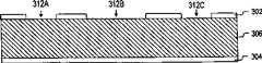
在步骤202中,如图5所示,氮化物层302和304分别被形成在衬底306的顶表面和底表面上。在一个实施例中,衬底306是厚度约675微米的硅,氮化物层302和304是通过低压化学气相沉积(LPCVD)形成的氮化硅(SiN4)并且具有约1000到2000埃的厚度。在一个实施例中,如果氮化物层302和304到硅衬底306的粘附变得有问题,则可以通过改进气体比例(二氯硅烷比氨)和气体的流量,使得氮化物层302和304具有低的应力。在一个实施例中,如果需要更加致密的氮化物层302和304来承受KOH刻蚀,则可以使得氮化物层302和304成为富硅的,以便变得更加致密。In
在步骤204中,如图6所示,随后将光刻胶308在氮化物层302上旋涂、曝光并且显影。图17示出了在一个实施例中用于该光刻工艺的掩模412。掩模412包括定义图9到16中的封盖腔314B的形状的封盖腔图案414。在一个实施例中,封盖腔图案414是梯形的,使得由非平行的侧面形成的侧壁是平坦的,而不是阶梯状的。掩模412还包括定义图9A和图10到16中的分离腔314A和314C的划线(scribe line)图案416。划线图案416沿着晶片306上提供对称刻蚀角度的方向取向。注意,图6到9A和图10到16示出了通过方法200沿线AA’形成的所得结构的横截面,而图9B示出了通过方法200沿线BB’形成的所得结构的横截面。In
在步骤206中,如图7所示,氮化物层302由光刻胶308中的窗口310A、310B和310C暴露的区域被向下刻蚀到衬底306。在一个实施例中,利用反应离子刻蚀(RIE)工艺刻蚀氮化物层302。氮化物层302的保留部分充当用于各向异性刻蚀的掩模。In
在步骤208中,如图8所示,光刻胶308被剥离。如可以看到的,窗口312A、312B和312C被形成在氮化物层302中。这些窗口的尺寸和它们之间的间隔取决于应用。In
在步骤210中,如在图9A中沿线AA’和在图9B中沿线BB’所示,衬底306被氮化物层302中的窗口312A到312C所暴露的区域被刻蚀,以形成分离腔314A和314C以及封盖腔314B。如可以在图9B中所看到的,封盖腔314B具有45度壁315(对应于图1中的表面132)和64.48度壁317。在一个实施例中,利用具有400比1的(100)面比(111)面选择性的KOH溶液各向异性地刻蚀硅衬底306。在一个实施例中,各腔被刻蚀到375微米深,这由于刻蚀剂的选择性而导致氮化物层302中的1微米的底切。In step 210, as shown along line AA' in FIG. 9A and along line BB' in FIG. 9B, the regions of
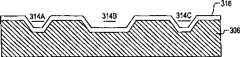
在步骤214中,如图10所示,氮化物层302和304被去除。在一个实施例中,利用热磷酸湿法刻蚀去除氮化物层302和304。In
在步骤216中,如图11所示,氧化物层316被形成在腔314A、314B和314C上方,并形成在衬底306的顶表面上。在一个实施例中,氧化物层316是从硅衬底306热生长的二氧化硅,并且具有约1000埃的厚度。In
在步骤218中,如图12所示,反射层320被形成在氧化物层316上方。在一个实施例中,反射层320是通过电子束蒸发或者溅射所沉积的钛-铂-金(TiPtAu)序列的金属堆叠。在一个实施例中,钛层具有约500埃的厚度,钛层顶上的铂层具有约1000埃的厚度,钛层顶上的金层具有约1500埃的厚度。金属堆叠320是在(111)面表面132(图1)上形成镜135(图1)的反射材料134(图1)。In
在步骤220中,如图12所示,阻挡层322被形成在反射层320上方。在一个实施例中,阻挡层322是被形成在反射层320上方的金属氧化物。例如,阻挡层322是热沉积在TiPtAu金属堆叠320上的二氧化钛(TiO2)层,并且具有约500埃的厚度。或者,阻挡层322可以是氮化物、硼化物、氟化物、碳氟化合物、聚酰亚胺或者可以承受焊接温度而不会粘附到焊料上的任何其他材料。此外,阻挡层322可以通过其他工艺来形成,包括溅射、反应溅射、化学气相沉积以及等离子体增强化学气相沉积。In
在步骤222中,如图13所示,光刻胶324然后被沉积(例如,被旋涂或者喷涂)在阻挡层322上。In
在步骤224中,如图14所示,光刻胶324被曝光和显影,以形成窗口326A、326B、326C和326D。阻挡层322由窗口326A到326D暴露的区域被向下刻蚀到反射层320。在一个实施例中,利用稀HF(1000∶1)和硝酸(100∶1)的溶液刻蚀二氧化钛阻挡层322。In
在步骤226中,如图15所示,焊料通过窗口326A到326D被镀覆到反射层320上。焊料在围绕封盖腔314B(也被示出为图1中的封盖腔131)的接合区域上形成密封环136(图1和2)。在一个实施例中,焊料是金-锡(AuSn)焊料,包括厚度为18500埃的金层328和金层328顶上的厚度为18500埃的锡层330。在一个实施例中,光刻胶324被剥离,再涂敷,并且再次图案化,以在镀覆焊料之前形成窗口326A到326D。这是因为金镀层(在底面上的)可以蘑菇状生成在用于金镀覆的初始光刻胶的顶面上。因此,为了得到一定程度的垂直边缘,可能有必要的是去除初始的光刻胶并且再涂敷将为焊料镀层提供形状的更厚的光刻胶。In
在步骤228中,如图16所示,光刻胶324被剥离并且封盖130现在可以被沿着虚拟线332与邻近的封盖130(部分示出)分离。In
图18示出了在本发明另一个实施例中形成晶片级封盖130的方法400。如可以看到的,方法400类似于方法200,除了用步骤426和428代替了步骤226和228。FIG. 18 illustrates a
在步骤426中,如图19所示,光刻胶324被剥离。这留下阻挡层322作为焊料镀覆过程中的掩模。In
在步骤428中,如图20所示,包括金层328和锡层330的焊料通过窗口326A到326D(现在由阻挡层322定义)被镀覆到反射层320上。同样,可以将封盖130沿着虚拟线332与邻近的封盖130(部分示出)分离。In
在方法200中,光刻胶324被留下作为焊料镀覆过程中的掩模。在方法400中,光刻胶324被剥离,并且阻挡层322被用作焊料镀覆过程中的掩模。方法400的优点在于光刻胶324不必是厚光刻胶。此外,光刻胶覆盖的均匀性是不重要的。注意,焊料和所得密封环136将发生少量的蘑菇状生长,因为焊料垂直生长与其横向生长大致相同的量。在一个实施例中,总的镀覆厚度为约3微米,因此横向生长不会带来问题。In
如上所述,TiO2可以被用作阻挡层。由于许多原因,TiO2在本应用中成为特别好的阻挡层。首先,AuSn焊料将不会粘附到其上。其次,其良好地粘附到金属堆叠中的金上,而没有多少材料可以这样。第三,虽然其具有可以改变金的反射率的高反射率,但是其可以沉积非常薄的层(例如,远小于四分之一波长)。在这样的厚度上,应该几乎不存在对于通过封盖的光传输的影响。另一个优点是所描述的方法在腔刻蚀之后仅仅要求一个掩模。这相对于在腔刻蚀之后常常要求多达三个掩模的其他方法提供了很大的成本优势。As mentioned above,TiO2 can be used as a barrier layer.TiO2 makes a particularly good barrier layer in this application for a number of reasons. First, AuSn solder will not adhere to it. Second, it adheres well to the gold in the metal stack, which not many materials do. Third, while it has a high reflectivity that can alter the reflectivity of gold, it can deposit very thin layers (eg, much less than a quarter wavelength). At such a thickness there should be little to no effect on light transmission through the cover. Another advantage is that the described method requires only one mask after cavity etching. This provides a significant cost advantage over other methods that often require as many as three masks after cavity etch.
虽然TiO2已经被公开为用于阻挡层的材料,但是其他具有下面特性的材料也可以被使用:(1)对镜(即,反射层)的良好粘附;(2)对焊料不可润湿;(3)透光;(4)以及不溶于镀覆溶液。AlthoughTiO2 has been disclosed as a material for the barrier layer, other materials with the following properties can also be used: (1) good adhesion to the mirror (i.e., reflective layer); (2) non-wettable to solder ; (3) light transmission; (4) and insoluble in the plating solution.
此外,阻挡层不必是薄的(例如,小于四分之一波长)。在一些应用中,具有厚的阻挡层是有利的。随着阻挡层达到四分之一波长附近的几何厚度(依赖于角度),反射能力的实质变化将变得明显。这些可能或多或少是反射性的。如果激光被准直,则这些干扰效应可以被用于提高镜的反射率。但是,如果激光没有被准直,则光的宽范围的角度将导致整个镜上依赖于局部角度的不同反射能力,这在光束离开镜时导致不同强度的光束。Furthermore, the blocking layer need not be thin (eg, less than a quarter wavelength). In some applications it is advantageous to have a thick barrier layer. Substantial changes in reflectivity will become apparent as the blocking layer reaches a geometric thickness in the vicinity of a quarter wavelength (angle dependent). These may be more or less reflective. If the laser light is collimated, these interference effects can be used to increase the reflectivity of the mirror. However, if the laser light is not collimated, the wide range of angles of the light will result in different reflectivity across the mirror depending on the local angle, which results in beams of different intensity as the beam leaves the mirror.
所公开的实施例的特征的各种其他修改和组合都在本发明的范围中。所附的权利要求覆盖了众多的实施例。Various other modifications and combinations of features of the disclosed embodiments are within the scope of the invention. The appended claims cover numerous embodiments.
Claims (21)
Translated fromChineseApplications Claiming Priority (2)
| Application Number | Priority Date | Filing Date | Title |
|---|---|---|---|
| US10/877,615US7045827B2 (en) | 2004-06-24 | 2004-06-24 | Lids for wafer-scale optoelectronic packages |
| US10/877,615 | 2004-06-24 |
Publications (2)
| Publication Number | Publication Date |
|---|---|
| CN1713468Atrue CN1713468A (en) | 2005-12-28 |
| CN1713468B CN1713468B (en) | 2011-10-05 |
Family
ID=35504672
Family Applications (1)
| Application Number | Title | Priority Date | Filing Date |
|---|---|---|---|
| CN2005100598904AExpired - Fee RelatedCN1713468B (en) | 2004-06-24 | 2005-04-01 | Cap for wafer-level optoelectronic packaging and method of manufacturing the same |
Country Status (4)
| Country | Link |
|---|---|
| US (3) | US7045827B2 (en) |
| JP (1) | JP4869634B2 (en) |
| CN (1) | CN1713468B (en) |
| DE (1) | DE102005010926B4 (en) |
Cited By (3)
| Publication number | Priority date | Publication date | Assignee | Title |
|---|---|---|---|---|
| CN100559559C (en)* | 2007-03-08 | 2009-11-11 | 探微科技股份有限公司 | Method for manufacturing optical element sealing cover |
| CN101599522B (en)* | 2009-06-30 | 2011-05-25 | 厦门市三安光电科技有限公司 | Vertical LED adopting insulating medium barrier layer and preparation method thereof |
| CN102119452A (en)* | 2008-08-11 | 2011-07-06 | 纳幕尔杜邦公司 | Light-emitting diode housing comprising fluoropolymer |
Families Citing this family (14)
| Publication number | Priority date | Publication date | Assignee | Title |
|---|---|---|---|---|
| US7750356B2 (en)* | 2005-05-04 | 2010-07-06 | Avago Technologies Fiber Ip (Singapore) Pte. Ltd. | Silicon optical package with 45 degree turning mirror |
| JP2009032843A (en)* | 2007-07-26 | 2009-02-12 | Nec Electronics Corp | Semiconductor device and manufacturing method therefor |
| JP2011222675A (en)* | 2010-04-07 | 2011-11-04 | Mitsubishi Electric Corp | Semiconductor device and method of manufacturing the same |
| US8582618B2 (en) | 2011-01-18 | 2013-11-12 | Avago Technologies General Ip (Singapore) Pte. Ltd. | Surface-emitting semiconductor laser device in which an edge-emitting laser is integrated with a diffractive or refractive lens on the semiconductor laser device |
| US8315287B1 (en) | 2011-05-03 | 2012-11-20 | Avago Technologies Fiber Ip (Singapore) Pte. Ltd | Surface-emitting semiconductor laser device in which an edge-emitting laser is integrated with a diffractive lens, and a method for making the device |
| JP2015503820A (en)* | 2011-12-22 | 2015-02-02 | スリーエム イノベイティブ プロパティズ カンパニー | Optical device with sensor, and method of manufacturing and using the same |
| DE102012217793A1 (en)* | 2012-09-28 | 2014-04-03 | Fraunhofer-Gesellschaft zur Förderung der angewandten Forschung e.V. | PRODUCTION METHOD |
| JP2014158157A (en)* | 2013-02-15 | 2014-08-28 | Asahi Kasei Electronics Co Ltd | Piezoelectric device |
| NO2944700T3 (en)* | 2013-07-11 | 2018-03-17 | ||
| US9793237B2 (en) | 2015-10-19 | 2017-10-17 | Qorvo Us, Inc. | Hollow-cavity flip-chip package with reinforced interconnects and process for making the same |
| US9799637B2 (en)* | 2016-02-12 | 2017-10-24 | Qorvo Us, Inc. | Semiconductor package with lid having lid conductive structure |
| EP3385762A1 (en) | 2017-04-03 | 2018-10-10 | Indigo Diabetes N.V. | Optical assembly with hermetically sealed cover cap |
| US10242967B2 (en) | 2017-05-16 | 2019-03-26 | Raytheon Company | Die encapsulation in oxide bonded wafer stack |
| JP6970336B2 (en)* | 2017-08-04 | 2021-11-24 | 日亜化学工業株式会社 | Light source device |
Family Cites Families (20)
| Publication number | Priority date | Publication date | Assignee | Title |
|---|---|---|---|---|
| US3657029A (en)* | 1968-12-31 | 1972-04-18 | Texas Instruments Inc | Platinum thin-film metallization method |
| US4773972A (en)* | 1986-10-30 | 1988-09-27 | Ford Motor Company | Method of making silicon capacitive pressure sensor with glass layer between silicon wafers |
| US4791075A (en)* | 1987-10-05 | 1988-12-13 | Motorola, Inc. | Process for making a hermetic low cost pin grid array package |
| JPH01264285A (en)* | 1988-04-15 | 1989-10-20 | Omron Tateisi Electron Co | Surface light-emitting type semiconductor laser |
| US5336928A (en)* | 1992-09-18 | 1994-08-09 | General Electric Company | Hermetically sealed packaged electronic system |
| US5500540A (en)* | 1994-04-15 | 1996-03-19 | Photonics Research Incorporated | Wafer scale optoelectronic package |
| DE4440935A1 (en)* | 1994-11-17 | 1996-05-23 | Ant Nachrichtentech | Optical transmitting and receiving device |
| EP0899781A3 (en) | 1997-08-28 | 2000-03-08 | Lucent Technologies Inc. | Corrosion protection in the fabrication of optoelectronic assemblies |
| US6062461A (en)* | 1998-06-03 | 2000-05-16 | Delphi Technologies, Inc. | Process for bonding micromachined wafers using solder |
| JP2000019357A (en)* | 1998-06-30 | 2000-01-21 | Toshiba Corp | Optical array module and reflector array |
| JP2000114655A (en)* | 1998-09-30 | 2000-04-21 | Toshiba Corp | Submount mirror type surface laser |
| DE19845484C2 (en)* | 1998-10-02 | 2002-09-26 | Infineon Technologies Ag | Micro-optical component and method for its production |
| US6818464B2 (en)* | 2001-10-17 | 2004-11-16 | Hymite A/S | Double-sided etching technique for providing a semiconductor structure with through-holes, and a feed-through metalization process for sealing the through-holes |
| TW560018B (en)* | 2001-10-30 | 2003-11-01 | Asia Pacific Microsystems Inc | A wafer level packaged structure and method for manufacturing the same |
| US7172911B2 (en)* | 2002-02-14 | 2007-02-06 | Silex Microsystems Ab | Deflectable microstructure and method of manufacturing the same through bonding of wafers |
| US6696645B2 (en)* | 2002-05-08 | 2004-02-24 | The Regents Of The University Of Michigan | On-wafer packaging for RF-MEMS |
| EP1517166B1 (en)* | 2003-09-15 | 2015-10-21 | Nuvotronics, LLC | Device package and methods for the fabrication and testing thereof |
| US20050063431A1 (en)* | 2003-09-19 | 2005-03-24 | Gallup Kendra J. | Integrated optics and electronics |
| US20050063648A1 (en)* | 2003-09-19 | 2005-03-24 | Wilson Robert Edward | Alignment post for optical subassemblies made with cylindrical rods, tubes, spheres, or similar features |
| US7767493B2 (en)* | 2005-06-14 | 2010-08-03 | John Trezza | Post & penetration interconnection |
- 2004
- 2004-06-24USUS10/877,615patent/US7045827B2/ennot_activeExpired - Lifetime
- 2005
- 2005-03-09DEDE102005010926Apatent/DE102005010926B4/ennot_activeExpired - Fee Related
- 2005-03-31USUS11/097,534patent/US7534636B2/ennot_activeExpired - Fee Related
- 2005-04-01CNCN2005100598904Apatent/CN1713468B/ennot_activeExpired - Fee Related
- 2005-06-03JPJP2005163977Apatent/JP4869634B2/ennot_activeExpired - Fee Related
- 2006
- 2006-01-18USUS11/335,091patent/US20060121635A1/ennot_activeAbandoned
Cited By (3)
| Publication number | Priority date | Publication date | Assignee | Title |
|---|---|---|---|---|
| CN100559559C (en)* | 2007-03-08 | 2009-11-11 | 探微科技股份有限公司 | Method for manufacturing optical element sealing cover |
| CN102119452A (en)* | 2008-08-11 | 2011-07-06 | 纳幕尔杜邦公司 | Light-emitting diode housing comprising fluoropolymer |
| CN101599522B (en)* | 2009-06-30 | 2011-05-25 | 厦门市三安光电科技有限公司 | Vertical LED adopting insulating medium barrier layer and preparation method thereof |
Also Published As
| Publication number | Publication date |
|---|---|
| DE102005010926B4 (en) | 2008-05-08 |
| JP2006013484A (en) | 2006-01-12 |
| JP4869634B2 (en) | 2012-02-08 |
| US20050285242A1 (en) | 2005-12-29 |
| DE102005010926A1 (en) | 2006-03-30 |
| US20050285131A1 (en) | 2005-12-29 |
| US7534636B2 (en) | 2009-05-19 |
| US20060121635A1 (en) | 2006-06-08 |
| US7045827B2 (en) | 2006-05-16 |
| CN1713468B (en) | 2011-10-05 |
Similar Documents
| Publication | Publication Date | Title |
|---|---|---|
| US20060121635A1 (en) | Lids for wafer-scale optoelectronic packages | |
| US11002907B2 (en) | Stepped optical bridge for connecting semiconductor waveguides | |
| CN110474230B (en) | Optoelectronic semiconductor component and method for producing an optoelectronic semiconductor component | |
| CN112771426A (en) | Method for III-V/silicon hybrid integration | |
| US20240128403A1 (en) | Micro light emitting element and its preparation method | |
| US6289030B1 (en) | Fabrication of semiconductor devices | |
| EP1854189A2 (en) | High reliability etched-facet photonic devices | |
| JP5404808B2 (en) | Light emitting element | |
| KR0172797B1 (en) | Laser diode and manufacturing method thereof | |
| CN119677260A (en) | LED chip and manufacturing method thereof | |
| CN115274967A (en) | Light-emitting diode chip with improved sorting damage and preparation method thereof | |
| WO2021185850A1 (en) | Coupon wafer and method of preparation thereof | |
| US20250271595A1 (en) | Metastructure optical elements, metastructure optical assemblies, and methods of manufacturing the same | |
| CN113471144B (en) | Method for manufacturing semiconductor device, semiconductor device and semiconductor substrate | |
| CN111641102B (en) | Semiconductor laser, bar and manufacturing method | |
| KR102873571B1 (en) | Air-gap encapsulation of nanostructured optical devices | |
| CN114023856B (en) | Light emitting diode and method of manufacturing the same | |
| CN116325388A (en) | Formation of semiconductor devices for non-hermetic environments | |
| CN120527755A (en) | Electroabsorption modulation semiconductor laser and preparation method thereof | |
| CN117239539A (en) | A high-speed chip with high reliability and its manufacturing process | |
| EP4445409A1 (en) | Method for manufacturing an optoelectronic device | |
| CN118448541A (en) | Light emitting diode and method for preparing light emitting diode | |
| KR101172555B1 (en) | Reflective layered system comprising a plurality of layers that are to be applied to a iii-v compound semiconductor material | |
| CN1248019C (en) | Fabrication method of MEMS Fabry-Perot device | |
| CN101569067A (en) | Etched-facet ridge laser with etch stop layer |
Legal Events
| Date | Code | Title | Description |
|---|---|---|---|
| C06 | Publication | ||
| PB01 | Publication | ||
| C41 | Transfer of patent application or patent right or utility model | ||
| TA01 | Transfer of patent application right | Effective date of registration:20061208 Address after:Singapore Singapore Applicant after:Avago Technologies ECBU IP Address before:Singapore Singapore Applicant before:Avago Technologies General IP (Singapore) Pte. Ltd. | |
| C10 | Entry into substantive examination | ||
| SE01 | Entry into force of request for substantive examination | ||
| C14 | Grant of patent or utility model | ||
| GR01 | Patent grant | ||
| ASS | Succession or assignment of patent right | Owner name:AVAGO TECHNOLOGIES GENERAL IP (SINGAPORE) CORPORAT Free format text:FORMER OWNER: AVAGO TECHNOLOGIES ECBU IP Effective date:20130509 | |
| C41 | Transfer of patent application or patent right or utility model | ||
| TR01 | Transfer of patent right | Effective date of registration:20130509 Address after:Singapore Singapore Patentee after:Avago Technologies Fiber IP Singapore Pte. Ltd. Address before:Singapore Singapore Patentee before:Avago Tech Fiber IP Sg Pte Ltd. | |
| C17 | Cessation of patent right | ||
| CF01 | Termination of patent right due to non-payment of annual fee | Granted publication date:20111005 Termination date:20140401 |