CN1679179A - A surface mounting type light emitting diode - Google Patents
A surface mounting type light emitting diodeDownload PDFInfo
- Publication number
- CN1679179A CN1679179ACN03820800.8ACN03820800ACN1679179ACN 1679179 ACN1679179 ACN 1679179ACN 03820800 ACN03820800 ACN 03820800ACN 1679179 ACN1679179 ACN 1679179A
- Authority
- CN
- China
- Prior art keywords
- light
- lead frame
- epoxy resin
- chip
- emitting diode
- Prior art date
- Legal status (The legal status is an assumption and is not a legal conclusion. Google has not performed a legal analysis and makes no representation as to the accuracy of the status listed.)
- Granted
Links
Images
Classifications
- H—ELECTRICITY
- H10—SEMICONDUCTOR DEVICES; ELECTRIC SOLID-STATE DEVICES NOT OTHERWISE PROVIDED FOR
- H10H—INORGANIC LIGHT-EMITTING SEMICONDUCTOR DEVICES HAVING POTENTIAL BARRIERS
- H10H20/00—Individual inorganic light-emitting semiconductor devices having potential barriers, e.g. light-emitting diodes [LED]
- H10H20/80—Constructional details
- H10H20/85—Packages
- H10H20/8506—Containers
- H—ELECTRICITY
- H01—ELECTRIC ELEMENTS
- H01L—SEMICONDUCTOR DEVICES NOT COVERED BY CLASS H10
- H01L2224/00—Indexing scheme for arrangements for connecting or disconnecting semiconductor or solid-state bodies and methods related thereto as covered by H01L24/00
- H01L2224/01—Means for bonding being attached to, or being formed on, the surface to be connected, e.g. chip-to-package, die-attach, "first-level" interconnects; Manufacturing methods related thereto
- H01L2224/26—Layer connectors, e.g. plate connectors, solder or adhesive layers; Manufacturing methods related thereto
- H01L2224/31—Structure, shape, material or disposition of the layer connectors after the connecting process
- H01L2224/32—Structure, shape, material or disposition of the layer connectors after the connecting process of an individual layer connector
- H01L2224/321—Disposition
- H01L2224/32151—Disposition the layer connector connecting between a semiconductor or solid-state body and an item not being a semiconductor or solid-state body, e.g. chip-to-substrate, chip-to-passive
- H01L2224/32221—Disposition the layer connector connecting between a semiconductor or solid-state body and an item not being a semiconductor or solid-state body, e.g. chip-to-substrate, chip-to-passive the body and the item being stacked
- H01L2224/32225—Disposition the layer connector connecting between a semiconductor or solid-state body and an item not being a semiconductor or solid-state body, e.g. chip-to-substrate, chip-to-passive the body and the item being stacked the item being non-metallic, e.g. insulating substrate with or without metallisation
- H—ELECTRICITY
- H01—ELECTRIC ELEMENTS
- H01L—SEMICONDUCTOR DEVICES NOT COVERED BY CLASS H10
- H01L2224/00—Indexing scheme for arrangements for connecting or disconnecting semiconductor or solid-state bodies and methods related thereto as covered by H01L24/00
- H01L2224/01—Means for bonding being attached to, or being formed on, the surface to be connected, e.g. chip-to-package, die-attach, "first-level" interconnects; Manufacturing methods related thereto
- H01L2224/26—Layer connectors, e.g. plate connectors, solder or adhesive layers; Manufacturing methods related thereto
- H01L2224/31—Structure, shape, material or disposition of the layer connectors after the connecting process
- H01L2224/32—Structure, shape, material or disposition of the layer connectors after the connecting process of an individual layer connector
- H01L2224/321—Disposition
- H01L2224/32151—Disposition the layer connector connecting between a semiconductor or solid-state body and an item not being a semiconductor or solid-state body, e.g. chip-to-substrate, chip-to-passive
- H01L2224/32221—Disposition the layer connector connecting between a semiconductor or solid-state body and an item not being a semiconductor or solid-state body, e.g. chip-to-substrate, chip-to-passive the body and the item being stacked
- H01L2224/32245—Disposition the layer connector connecting between a semiconductor or solid-state body and an item not being a semiconductor or solid-state body, e.g. chip-to-substrate, chip-to-passive the body and the item being stacked the item being metallic
- H—ELECTRICITY
- H01—ELECTRIC ELEMENTS
- H01L—SEMICONDUCTOR DEVICES NOT COVERED BY CLASS H10
- H01L2224/00—Indexing scheme for arrangements for connecting or disconnecting semiconductor or solid-state bodies and methods related thereto as covered by H01L24/00
- H01L2224/01—Means for bonding being attached to, or being formed on, the surface to be connected, e.g. chip-to-package, die-attach, "first-level" interconnects; Manufacturing methods related thereto
- H01L2224/42—Wire connectors; Manufacturing methods related thereto
- H01L2224/44—Structure, shape, material or disposition of the wire connectors prior to the connecting process
- H01L2224/45—Structure, shape, material or disposition of the wire connectors prior to the connecting process of an individual wire connector
- H01L2224/45001—Core members of the connector
- H01L2224/45099—Material
- H01L2224/451—Material with a principal constituent of the material being a metal or a metalloid, e.g. boron (B), silicon (Si), germanium (Ge), arsenic (As), antimony (Sb), tellurium (Te) and polonium (Po), and alloys thereof
- H01L2224/45138—Material with a principal constituent of the material being a metal or a metalloid, e.g. boron (B), silicon (Si), germanium (Ge), arsenic (As), antimony (Sb), tellurium (Te) and polonium (Po), and alloys thereof the principal constituent melting at a temperature of greater than or equal to 950°C and less than 1550°C
- H01L2224/45144—Gold (Au) as principal constituent
- H—ELECTRICITY
- H01—ELECTRIC ELEMENTS
- H01L—SEMICONDUCTOR DEVICES NOT COVERED BY CLASS H10
- H01L2224/00—Indexing scheme for arrangements for connecting or disconnecting semiconductor or solid-state bodies and methods related thereto as covered by H01L24/00
- H01L2224/01—Means for bonding being attached to, or being formed on, the surface to be connected, e.g. chip-to-package, die-attach, "first-level" interconnects; Manufacturing methods related thereto
- H01L2224/42—Wire connectors; Manufacturing methods related thereto
- H01L2224/47—Structure, shape, material or disposition of the wire connectors after the connecting process
- H01L2224/48—Structure, shape, material or disposition of the wire connectors after the connecting process of an individual wire connector
- H01L2224/481—Disposition
- H01L2224/48151—Connecting between a semiconductor or solid-state body and an item not being a semiconductor or solid-state body, e.g. chip-to-substrate, chip-to-passive
- H01L2224/48221—Connecting between a semiconductor or solid-state body and an item not being a semiconductor or solid-state body, e.g. chip-to-substrate, chip-to-passive the body and the item being stacked
- H01L2224/48225—Connecting between a semiconductor or solid-state body and an item not being a semiconductor or solid-state body, e.g. chip-to-substrate, chip-to-passive the body and the item being stacked the item being non-metallic, e.g. insulating substrate with or without metallisation
- H01L2224/48227—Connecting between a semiconductor or solid-state body and an item not being a semiconductor or solid-state body, e.g. chip-to-substrate, chip-to-passive the body and the item being stacked the item being non-metallic, e.g. insulating substrate with or without metallisation connecting the wire to a bond pad of the item
- H—ELECTRICITY
- H01—ELECTRIC ELEMENTS
- H01L—SEMICONDUCTOR DEVICES NOT COVERED BY CLASS H10
- H01L2224/00—Indexing scheme for arrangements for connecting or disconnecting semiconductor or solid-state bodies and methods related thereto as covered by H01L24/00
- H01L2224/01—Means for bonding being attached to, or being formed on, the surface to be connected, e.g. chip-to-package, die-attach, "first-level" interconnects; Manufacturing methods related thereto
- H01L2224/42—Wire connectors; Manufacturing methods related thereto
- H01L2224/47—Structure, shape, material or disposition of the wire connectors after the connecting process
- H01L2224/48—Structure, shape, material or disposition of the wire connectors after the connecting process of an individual wire connector
- H01L2224/481—Disposition
- H01L2224/48151—Connecting between a semiconductor or solid-state body and an item not being a semiconductor or solid-state body, e.g. chip-to-substrate, chip-to-passive
- H01L2224/48221—Connecting between a semiconductor or solid-state body and an item not being a semiconductor or solid-state body, e.g. chip-to-substrate, chip-to-passive the body and the item being stacked
- H01L2224/48245—Connecting between a semiconductor or solid-state body and an item not being a semiconductor or solid-state body, e.g. chip-to-substrate, chip-to-passive the body and the item being stacked the item being metallic
- H01L2224/48247—Connecting between a semiconductor or solid-state body and an item not being a semiconductor or solid-state body, e.g. chip-to-substrate, chip-to-passive the body and the item being stacked the item being metallic connecting the wire to a bond pad of the item
- H—ELECTRICITY
- H01—ELECTRIC ELEMENTS
- H01L—SEMICONDUCTOR DEVICES NOT COVERED BY CLASS H10
- H01L2224/00—Indexing scheme for arrangements for connecting or disconnecting semiconductor or solid-state bodies and methods related thereto as covered by H01L24/00
- H01L2224/01—Means for bonding being attached to, or being formed on, the surface to be connected, e.g. chip-to-package, die-attach, "first-level" interconnects; Manufacturing methods related thereto
- H01L2224/42—Wire connectors; Manufacturing methods related thereto
- H01L2224/47—Structure, shape, material or disposition of the wire connectors after the connecting process
- H01L2224/48—Structure, shape, material or disposition of the wire connectors after the connecting process of an individual wire connector
- H01L2224/484—Connecting portions
- H01L2224/48463—Connecting portions the connecting portion on the bonding area of the semiconductor or solid-state body being a ball bond
- H01L2224/48465—Connecting portions the connecting portion on the bonding area of the semiconductor or solid-state body being a ball bond the other connecting portion not on the bonding area being a wedge bond, i.e. ball-to-wedge, regular stitch
- H—ELECTRICITY
- H01—ELECTRIC ELEMENTS
- H01L—SEMICONDUCTOR DEVICES NOT COVERED BY CLASS H10
- H01L2224/00—Indexing scheme for arrangements for connecting or disconnecting semiconductor or solid-state bodies and methods related thereto as covered by H01L24/00
- H01L2224/73—Means for bonding being of different types provided for in two or more of groups H01L2224/10, H01L2224/18, H01L2224/26, H01L2224/34, H01L2224/42, H01L2224/50, H01L2224/63, H01L2224/71
- H01L2224/732—Location after the connecting process
- H01L2224/73251—Location after the connecting process on different surfaces
- H01L2224/73265—Layer and wire connectors
- H—ELECTRICITY
- H01—ELECTRIC ELEMENTS
- H01L—SEMICONDUCTOR DEVICES NOT COVERED BY CLASS H10
- H01L2924/00—Indexing scheme for arrangements or methods for connecting or disconnecting semiconductor or solid-state bodies as covered by H01L24/00
- H01L2924/10—Details of semiconductor or other solid state devices to be connected
- H01L2924/11—Device type
- H01L2924/13—Discrete devices, e.g. 3 terminal devices
- H01L2924/1301—Thyristor
- H01L2924/13033—TRIAC - Triode for Alternating Current - A bidirectional switching device containing two thyristor structures with common gate contact
- H—ELECTRICITY
- H01—ELECTRIC ELEMENTS
- H01L—SEMICONDUCTOR DEVICES NOT COVERED BY CLASS H10
- H01L2924/00—Indexing scheme for arrangements or methods for connecting or disconnecting semiconductor or solid-state bodies as covered by H01L24/00
- H01L2924/10—Details of semiconductor or other solid state devices to be connected
- H01L2924/11—Device type
- H01L2924/13—Discrete devices, e.g. 3 terminal devices
- H01L2924/1301—Thyristor
- H01L2924/13034—Silicon Controlled Rectifier [SCR]
- H—ELECTRICITY
- H10—SEMICONDUCTOR DEVICES; ELECTRIC SOLID-STATE DEVICES NOT OTHERWISE PROVIDED FOR
- H10H—INORGANIC LIGHT-EMITTING SEMICONDUCTOR DEVICES HAVING POTENTIAL BARRIERS
- H10H20/00—Individual inorganic light-emitting semiconductor devices having potential barriers, e.g. light-emitting diodes [LED]
- H10H20/80—Constructional details
- H10H20/85—Packages
- H10H20/852—Encapsulations
- H10H20/853—Encapsulations characterised by their shape
- H—ELECTRICITY
- H10—SEMICONDUCTOR DEVICES; ELECTRIC SOLID-STATE DEVICES NOT OTHERWISE PROVIDED FOR
- H10H—INORGANIC LIGHT-EMITTING SEMICONDUCTOR DEVICES HAVING POTENTIAL BARRIERS
- H10H20/00—Individual inorganic light-emitting semiconductor devices having potential barriers, e.g. light-emitting diodes [LED]
- H10H20/80—Constructional details
- H10H20/85—Packages
- H10H20/855—Optical field-shaping means, e.g. lenses
- H10H20/856—Reflecting means
- H—ELECTRICITY
- H10—SEMICONDUCTOR DEVICES; ELECTRIC SOLID-STATE DEVICES NOT OTHERWISE PROVIDED FOR
- H10H—INORGANIC LIGHT-EMITTING SEMICONDUCTOR DEVICES HAVING POTENTIAL BARRIERS
- H10H20/00—Individual inorganic light-emitting semiconductor devices having potential barriers, e.g. light-emitting diodes [LED]
- H10H20/80—Constructional details
- H10H20/85—Packages
- H10H20/857—Interconnections, e.g. lead-frames, bond wires or solder balls
Landscapes
- Led Device Packages (AREA)
Abstract
Description
Translated fromChinese技术领域technical field
本发明是关于表面安装型发光二极管(A Surface Mounting Type LightEmitting Diode)的发明。具体说明如下:用发光的InGaN、GaN发光二极管芯片在镀银的导线架的杯状焊盘上采用芯片键合法,然后可以增加微型封装部件的光反射率和光亮度。The present invention relates to the invention of surface mount type light emitting diode (A Surface Mounting Type LightEmitting Diode). The specific instructions are as follows: use luminous InGaN and GaN light-emitting diode chips on the cup-shaped pads of the silver-plated lead frame to adopt the chip bonding method, and then the light reflectivity and brightness of the micro-packaged components can be increased.
背景技术Background technique
一般来讲,光半导体元件(发光二极管)是通过电信号用于光传送的部件,分别是:通过发光二极管把电信号转换成光信号后通过腔体前部发光的发光元件(350nm-990nm)和接收光信号后转换成电信号的光敏元件(光敏晶体管、光敏二极管、光敏可控硅、光敏IC)等。这些光半导体元件根据构成PN结的掺杂物质的材质、种类、密度和构造,可制造出从紫外光到可见光、红外光等各种波长的产品。Generally speaking, optical semiconductor elements (light-emitting diodes) are components used for light transmission through electrical signals, namely: light-emitting elements (350nm-990nm) that convert electrical signals into optical signals through light-emitting diodes and then emit light through the front of the cavity And photosensitive elements (phototransistors, photodiodes, photosensitive thyristors, photosensitive ICs) that convert into electrical signals after receiving optical signals. These optical semiconductor elements can be manufactured in various wavelengths from ultraviolet light to visible light and infrared light according to the material, type, density, and structure of the dopant substance that constitutes the PN junction.
可见光发光二极管是利用PN结的注入电致发光(injection ElectroLuminescence)原理的发光元件,由于其发光所需的外加电压非常低,而且寿命长,所以广泛应用于固体指示元件、显像指示等领域的半导体元件中。Visible light-emitting diodes are light-emitting elements that use the principle of injection ElectroLuminescence of the PN junction. Because the external voltage required for light emission is very low and the service life is long, it is widely used in the fields of solid-state indicating elements, imaging indicators, etc. in semiconductor components.
可见光光半导体元件可以制作成各种封装的部件,具有代表性的是:适用于手机背光(Back Light)的表面安装型微型发光二极管(Chip LED)元件和电子标示及固体指示元件或显像指示用的3φ、5φ立式灯类元件。Visible light semiconductor components can be made into various packaged components, and the representative ones are: surface-mounted micro-light-emitting diode (Chip LED) components suitable for mobile phone backlight (Back Light) components and electronic signs and solid indicator components or display indicators 3φ, 5φ vertical lamp components used.
下面以可见光发光二极管为例对表面安装型微型发光二极管元件加以详细说明。The surface-mounted miniature light-emitting diode components will be described in detail below by taking visible light-emitting diodes as an example.
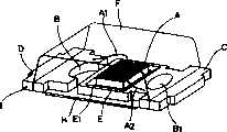
传统的表面安装型发光二极管的构造如图1所示,外加电压时发光的芯片(A)和给上述芯片(A)外加电压时所用的导电性金属材料的阴极和阳极导线(C)(D)组成。所述芯片(A)与阴极导线(C)顶端部位所形成的芯片焊盘(DiePad)(E1)用银粘合剂(E2)粘合,同时,芯片(A)与阴极/阳极导线的末端以及导线(A2)(A1)键合(bongding),然后在阴极和阳极发光二极管导线(C)(D)之间电气连接。The structure of a traditional surface-mounted light-emitting diode is shown in Figure 1. The chip (A) that emits light when an external voltage is applied and the cathode and anode wires (C) (D) of conductive metal materials used when applying a voltage to the above-mentioned chip (A) )composition. The die pad (DiePad) (E1) formed on the tip of the chip (A) and the cathode wire (C) is bonded with a silver adhesive (E2), and at the same time, the chip (A) is bonded to the end of the cathode/anode wire And wires (A2)(A1) are bonded (bongding), and then electrically connected between the cathode and anode LED wires (C)(D).
而且,为了从外部保护上述芯片(A),用绝缘材质的透光的涂覆材料(F)对芯片(A)进行涂覆,使阴极和阳极发光二极管导线(C)(D)的另一末端露出,使得能从外部向芯片(A)施加电压。Moreover, in order to protect the above-mentioned chip (A) from the outside, the chip (A) is coated with a light-transmitting coating material (F) of an insulating material, so that the cathode and the anode light-emitting diode wire (C) (D) another The ends are exposed so that voltage can be applied to the chip (A) from the outside.
若把外露的发光二极管的阴极与阳极端导线(C)(D)与正要使用的电路电气连接,当电源通过阴极和阳极导线(C)(D)施加到芯片(A)上时,光半导体元件的芯片(A)发光,使其发挥功能。涂覆材料(F)通常是由透明环氧树脂(Epoxy)构成,根据发光二极管芯片种类的不同,产生红色、绿色、蓝色、桔色等。If the cathode and anode terminal wires (C) (D) of the exposed light-emitting diodes are electrically connected to the circuit to be used, when the power is applied to the chip (A) through the cathode and anode wires (C) (D), the light The chip (A) of the semiconductor element emits light to function. The coating material (F) is usually made of transparent epoxy resin (Epoxy), which can produce red, green, blue, orange, etc. according to different types of LED chips.
上述具有代表性的传统表面安装型微型发光二极管元件是以很厚的PCB基板(J)构成。这种PCB基板(J)耐热性能非常低。所以在发光二极管制造流程中,由于热压力会产生PCB基板(J)的热变形,导致PCB的环氧树脂的粘合力降低,从而无法保障其牢固度。因为保障其牢固度的工艺流程很复杂,所以会导致制造费用增加。而且,由于使用很厚的PCB,不能实现微型芯片LED的轻薄化。另外,若使用此方法会降低PCB基板的光反射率、芯片焊盘镀的金的光反射率也很低,因而会导致面发光芯片(InGaN、GaN的LED芯片)(390nm-470nm)光亮度降低的问题。由于这种PCB基板100%都要依靠进口,原材料价格很高。而且要使用贵金属—金,所以制造费用是很昂贵的。The above-mentioned representative conventional surface-mounted miniature light-emitting diode components are composed of a very thick PCB substrate (J). This PCB substrate (J) has very low heat resistance. Therefore, in the manufacturing process of the light-emitting diode, due to the thermal deformation of the PCB substrate (J) due to thermal pressure, the adhesive force of the epoxy resin of the PCB is reduced, so that its firmness cannot be guaranteed. Because the technological process for ensuring its firmness is very complicated, it will lead to an increase in manufacturing costs. Moreover, since a very thick PCB is used, thinning and lightening of microchip LEDs cannot be achieved. In addition, if this method is used, the light reflectivity of the PCB substrate will be reduced, and the light reflectivity of the gold plated on the chip pad will also be very low, which will lead to the brightness of surface emitting chips (InGaN, GaN LED chips) (390nm-470nm) Lowering the problem. Since this PCB substrate is 100% dependent on imports, the price of raw materials is very high. Moreover, precious metal—gold is used, so the manufacturing cost is very expensive.
并且,在手机等领域里,通过回流焊接(Solder Reflow)工艺安装芯片LED光元件,这种回流焊接工艺在220℃-320℃的作业条件下进行。可是PCB基板的热变形温度是220℃以下,所以回流焊接工艺会给传统的表面安装型(SMD)的微型发光二极管(Chip LED)元件带来致命的热冲击,导致金质导线(A1)(A2)和银环氧树脂(E2)从PCB基板上脱落下来。由此可见,传统的表面安装型(SDM)微型芯片LED元件很难保障其使用寿命。Moreover, in the field of mobile phones and other fields, chip LED optical components are installed by reflow soldering (Solder Reflow) process, and this reflow soldering process is carried out under the operating conditions of 220°C-320°C. However, the thermal deformation temperature of the PCB substrate is below 220°C, so the reflow soldering process will bring fatal thermal shock to the traditional surface mount (SMD) micro light-emitting diode (Chip LED) components, resulting in gold wires (A1)( A2) and silver epoxy (E2) came off the PCB substrate. It can be seen that the traditional surface mount type (SDM) microchip LED components are difficult to guarantee their service life.
发明内容Contents of the invention
本发明是为了解决上述传统表面安装型微型发光二极管元件的诸多问题。将表面发光芯片(InGaN、GaN的LED芯片)(390nm-470nm)用绝缘性的透光的芯片粘合剂(紫外粘合剂、绝缘透明粘合剂)粘附在导线架的杯状焊盘上,避免了使用银环氧粘合剂,彻底解决阳极和阴极之间的短路问题。发射面的反方向释放的光,通过绝缘的透光的环氧粘合剂进行透射,使这个透射光在反射率极高的镀银芯片焊盘上得到反射,并集中到发射方向上,从而增加光的亮度。The present invention aims to solve many problems of the above-mentioned conventional surface-mounted miniature light-emitting diode elements. Adhere the surface light-emitting chip (InGaN, GaN LED chip) (390nm-470nm) to the cup-shaped pad of the lead frame with an insulating light-transmitting chip adhesive (UV adhesive, insulating transparent adhesive) In addition, the use of silver epoxy adhesive is avoided, and the problem of short circuit between anode and cathode is completely solved. The light released in the opposite direction of the emitting surface is transmitted through the insulating light-transmitting epoxy adhesive, so that the transmitted light is reflected on the silver-plated chip pad with extremely high reflectivity and concentrated in the emitting direction, thereby Increases the brightness of the light.
本发明的另一目的是,以很薄的引线架作为基板,采用透光的环氧树脂涂覆在导线架上,使透光的环氧树脂下面的环氧树脂比导线架部件的相同平面突出10-50μm,再通过贯通孔使上面的透光的环氧树脂与下面的环氧树脂连接起来,使光元件的热冲击力达到最小化,从而提供超薄的芯片LED。Another object of the present invention is to use a very thin lead frame as the substrate, and use light-transmitting epoxy resin to coat the lead frame, so that the epoxy resin under the light-transmitting epoxy resin is lower than the same plane of the lead frame parts. Protrude by 10-50μm, and connect the upper light-transmitting epoxy resin with the lower epoxy resin through the through hole, so as to minimize the thermal shock force of the optical element, thereby providing ultra-thin chip LEDs.
本发明的另一个目的是在高温220℃-320℃状态下,机械装置(setmachinery)回流焊接工艺的热压力达到最小化,从而解决了由于表面安装型微型发光二极管元件遭到致命的热冲击,使金质导线和银环氧树脂从PCB板上脱落的传统技术难点。传统技术很难保证表面安装型微型LED元件的寿命,本发明通过使用热变形温度在450℃以上的耐热性导线架基板,从而提供了保障光半导体元件的寿命和热冲击最小化的微型发光二极管。Another object of the present invention is to minimize the thermal pressure of the setmachinery reflow soldering process at a high temperature of 220°C-320°C, thereby solving the fatal thermal shock caused by surface-mounted micro-LED components. The traditional technical difficulty of making the gold wire and silver epoxy come off the PCB board. It is difficult to ensure the life of surface-mounted micro-LED elements in conventional technologies. The present invention provides micro-luminescence that guarantees the life of optical semiconductor elements and minimizes thermal shock by using a heat-resistant lead frame substrate with a heat distortion temperature of 450°C or higher. diode.
本发明还有一个目的是:传统的PCB板(J)作为高价的基板材料并且只有在芯片焊盘镀金后才能使用,而且PCB板100%依靠进口,所以制造费用非常昂贵。上述发明提供了使用低价镀银导线架基板,而有效节省制造成本的微型发光二极管元件。Another purpose of the present invention is: the traditional PCB board (J) is used as a high-priced substrate material and can only be used after the chip pad is gold-plated, and the PCB board is 100% dependent on imports, so the manufacturing cost is very expensive. The above invention provides a miniature light-emitting diode element that effectively saves manufacturing cost by using a low-priced silver-plated lead frame substrate.
为了达到上述目的而发明的微型超薄发光二极管光半导体元件,每一对结构部件作为多数量中的一组,由很多的列排列而成,每个单元导线架是以绝缘型透光的环氧粘合剂作点粘合,使用粘合剂,把光元件芯片(350nm-470nm)与杯状焊盘采用芯片键合法(Die Bonding),通过金质导线将上述导线架的框架部位与光元件芯片的电极相连接,将导线架的框架部位发光二极管的安全地安装在压模机上,透光的环氧树脂涂覆,涂覆结束后将一系列的导线架部件粘合在粘合剂上,然后用金刚石刀片将其切断,通过特定工艺流程完成制作。For the miniature ultra-thin light-emitting diode photo-semiconductor element invented in order to achieve the above-mentioned purpose, each pair of structural parts is arranged as a group in a large number, and is arranged in many columns, and each unit lead frame is an insulating light-transmitting ring Oxygen adhesive is used for point bonding, using adhesive, the optical element chip (350nm-470nm) and the cup-shaped pad are bonded by the die bonding method (Die Bonding), and the frame part of the above-mentioned lead frame is connected to the optical The electrodes of the component chips are connected, and the light-emitting diodes on the frame part of the lead frame are safely installed on the molding machine, and the light-transmitting epoxy resin is coated. After the coating is completed, a series of lead frame parts are bonded to the adhesive. Then cut it off with a diamond blade, and complete the production through a specific process.
附图说明Description of drawings
图1为传统表面安装型发光二极管构造的图示;FIG. 1 is a schematic diagram of the structure of a conventional surface-mounted light-emitting diode;
图2为按照本发明的表面安装型发光二极管图示。Fig. 2 is a schematic diagram of a surface mount type light emitting diode according to the present invention.
具体实施方式Detailed ways
下面参照附图,将对本发明微型超薄芯片LED光半导体元件加以说明。Referring to the accompanying drawings, the micro-ultra-thin chip LED photo-semiconductor element of the present invention will be described below.
图2所示的是根据本发明的一个实例微型超薄发光二极管的内部构造的横截面的图示。如图所示,本发明微型超薄发光二极管由以下几部分构成:一对阳极导线架(Anode Lead Frame)(D)和阴极导线架(Cathode LeadFrame)(C)组成的导线架(I);使阳极/阴极导线架(D)(C)和发光二极管芯片(A)通电用的导线(A1)(A2);涂敷在两个导线架(D)(C)上部的透光环氧树脂(F);在导线架(C)(D)下端形成10-50μm突起的下面的环氧树脂(H);连接下面的环氧树脂(H)和与之相对应的上面的透光的环氧树脂(F)的阳极导线贯通孔(B)与阴极导线贯通孔(B1)。FIG. 2 is a cross-sectional illustration of the internal structure of a miniature ultra-thin light emitting diode according to an example of the present invention. As shown in the figure, the miniature ultra-thin light-emitting diode of the present invention is made up of following several parts: a pair of anode lead frame (Anode Lead Frame) (D) and the lead frame (I) that cathode lead frame (Cathode Lead Frame) (C) is formed; Lead wires (A1)(A2) for anode/cathode lead frames (D)(C) and light-emitting diode chips (A) to be energized; light-transmitting epoxy resin coated on the upper part of the two lead frames (D)(C) (F); form the lower epoxy resin (H) with 10-50 μm protrusions at the lower end of the lead frame (C) (D); connect the lower epoxy resin (H) and the corresponding upper light-transmitting ring An anode wire through hole (B) and a cathode wire through hole (B1) of the epoxy resin (F).
下面简要说明本发明中芯片LED光半导体元件制作工艺流程。即:把成对的阴、阳极导线架排列多列作为一组的工艺流程;每对单元导线架用绝缘的透光的环氧粘合剂作点粘合(Dotting)的工艺流程;用粘合剂将光元件芯片(390nm-470nm芯片)在导线架焊盘部位采用芯片键合法(Die Bonding)的工艺流程;通过金质导线将上述导线架与光元件芯片的电极相连接的工艺流程;将导线架部件安全地安装在压模机上,通过透光的环氧树脂涂覆的工艺流程;涂覆结束后,将各列导线架部件用粘合剂粘好,然后用金刚石刀片(Blade)将其切断,最后经过特定工艺流程完成制作。The following briefly describes the manufacturing process flow of the chip LED optical semiconductor element in the present invention. That is: the process flow of arranging pairs of cathode and anode lead frames in multiple rows as a group; the process flow of dotting each pair of unit lead frames with insulating light-transmitting epoxy adhesive; Die Bonding process of the optical element chip (390nm-470nm chip) on the pad of the lead frame; the process flow of connecting the above lead frame to the electrode of the optical element chip through a gold wire; Safely install the lead frame components on the molding machine, and pass through the process flow of light-transmitting epoxy resin coating; after coating, each column of lead frame components is glued with adhesive, and then the diamond blade (Blade) is used to Cut it off, and finally complete the production through a specific process.
将表面发光芯片(InGaN、GaN的LED芯片)(390nm-470nm)用绝缘性的透光的涂覆粘合剂(E)(紫外(UV cure)粘合剂、绝缘透明粘合剂),粘合在发光二极管芯片杯状焊盘(E1)上,避免了银环氧粘合剂的使用,彻底解决阳极和阴极间的短路问题。在表面发光芯片释放的光中,把从发射面反方向释放的光通过绝缘透光的环氧粘合剂进行透射,这个透射光在反射率很高的镀银芯片杯状焊盘上反射,聚焦在光出射方向,从而增加光亮度。Surface light-emitting chips (InGaN, GaN LED chips) (390nm-470nm) are coated with an insulating light-transmitting adhesive (E) (ultraviolet (UV cure) adhesive, insulating transparent adhesive), and glued It is combined on the cup-shaped pad (E1) of the light-emitting diode chip, avoiding the use of silver epoxy adhesive, and completely solving the short circuit problem between the anode and the cathode. In the light released by the surface emitting chip, the light released from the opposite direction of the emitting surface is transmitted through the insulating light-transmitting epoxy adhesive, and the transmitted light is reflected on the silver-plated chip cup-shaped pad with high reflectivity, Focusing on the light exit direction, thus increasing the brightness of the light.
本发明使用了很薄的导线架(I)基板,涂覆时把导线架(I)和透光的环氧树脂(F)的下面的环氧树脂(H)的形成比导线架的导线部件相同平面状突起10-50μm,用贯通孔(B)(B1)将上部的透光的环氧树脂(F)与下面的环氧树脂(H)连接起来,使光元件的热冲击达到最小化。The present invention has used very thin lead frame (I) substrate, and the epoxy resin (H) below the lead frame (I) and light-transmitting epoxy resin (F) is formed into the lead parts of lead frame when coating The same planar protrusion is 10-50μm, and the upper light-transmitting epoxy resin (F) is connected with the lower epoxy resin (H) with the through hole (B) (B1) to minimize the thermal shock of the optical element .
本发明使用了热变形温度在450℃以上的耐热性导线架(I)基板,保证了光半导体元件的寿命和热冲击达到最小化,而且用价格低廉的镀银板作为导线架基板,有效地降低了制造成本。The present invention uses the heat-resistant lead frame (I) substrate with a heat distortion temperature above 450°C, which ensures that the life of the optical semiconductor element and thermal shock are minimized, and uses a cheap silver-plated plate as the lead frame substrate, effectively reduce the manufacturing cost.
工业适应性Industrial adaptability
本发明把表面发光芯片用绝缘性的透光的粘合剂粘合在发光二极管的芯片安装板上,避免了银环氧粘合剂的使用,彻底解决阳极和阴极间的短路问题。在表面发光芯片释放的光中,把发射面的反方向释放的光通过绝缘的透光的环氧粘合剂进行透射,这种透射光在反射率很高的镀银芯片杯状焊盘上反射,光聚焦在出射方向,从而增加光亮度;通过使用很薄的导线架基板,用透光的环氧树脂涂敷,使透光的环氧树脂的下面的环氧树脂,比导线架的导线部分的相同平面突出10-50μm,用贯通孔将上部的透光的环氧树脂与下面的环氧树脂连接起来,使光元件的热冲击力达到最小化,实现超薄型的芯片LED;使高温状态使用的机械装置,在回流焊接工艺流程(220℃-320℃)中达到热压力最小化,从而解决了由于表面安装型(SMD)微型发光二极管元件受到致命的热冲击力而造成的金质导线和银环氧树脂从PCB板上脱落的传统技术难点;通过使用热变形温度在450℃以上的耐热性导线架基板,保证了光半导体元件的寿命和热冲击力达到最小化,实现了超薄化的效果。In the invention, the surface light-emitting chip is bonded to the chip mounting board of the light-emitting diode with an insulating light-transmitting adhesive, avoiding the use of silver epoxy adhesive, and completely solving the short circuit problem between the anode and the cathode. In the light released by the surface emitting chip, the light released in the opposite direction of the emitting surface is transmitted through the insulating light-transmitting epoxy adhesive, and this transmitted light is on the silver-plated chip cup pad with high reflectivity Reflection, the light is focused in the outgoing direction, thereby increasing the brightness; by using a very thin lead frame substrate, coated with light-transmitting epoxy resin, the epoxy resin under the light-transmitting epoxy resin is less than that of the lead frame The same plane of the wire part protrudes 10-50μm, and the upper light-transmitting epoxy resin is connected with the lower epoxy resin with a through hole, so as to minimize the thermal shock force of the optical element and realize an ultra-thin chip LED; The mechanical device used in the high temperature state minimizes the thermal stress in the reflow soldering process (220°C-320°C), thereby solving the problem caused by the fatal thermal shock force of the surface mount type (SMD) miniature light-emitting diode components. The traditional technical difficulty that the gold wire and silver epoxy resin fall off from the PCB board; by using a heat-resistant lead frame substrate with a heat distortion temperature above 450°C, the life of the optical semiconductor element and the thermal shock force are minimized, Achieved the effect of ultra-thinning.
Claims (2)
Translated fromChineseApplications Claiming Priority (2)
| Application Number | Priority Date | Filing Date | Title |
|---|---|---|---|
| KR2020020026208 | 2002-09-02 | ||
| KR20-2002-0026208UKR200299491Y1 (en) | 2002-09-02 | 2002-09-02 | A Surface mounting type light emitting diode |
Publications (2)
| Publication Number | Publication Date |
|---|---|
| CN1679179Atrue CN1679179A (en) | 2005-10-05 |
| CN100379036C CN100379036C (en) | 2008-04-02 |
Family
ID=36383850
Family Applications (1)
| Application Number | Title | Priority Date | Filing Date |
|---|---|---|---|
| CNB038208008AExpired - Fee RelatedCN100379036C (en) | 2002-09-02 | 2003-09-01 | Surface Mount Light Emitting Diodes |
Country Status (5)
| Country | Link |
|---|---|
| JP (1) | JP2006514426A (en) |
| KR (1) | KR200299491Y1 (en) |
| CN (1) | CN100379036C (en) |
| AU (1) | AU2003258842A1 (en) |
| WO (1) | WO2004036660A1 (en) |
Cited By (6)
| Publication number | Priority date | Publication date | Assignee | Title |
|---|---|---|---|---|
| CN100487933C (en)* | 2006-02-23 | 2009-05-13 | 宏齐科技股份有限公司 | Packaging structure and packaging method of light emitting diode |
| CN101459211B (en)* | 2007-12-11 | 2011-03-02 | 富士迈半导体精密工业(上海)有限公司 | Solid illuminating device |
| CN102129986A (en)* | 2010-12-29 | 2011-07-20 | 朝阳无线电元件有限责任公司 | Method for manufacturing glass sealed diode by adopting metallurgy bonding method |
| CN102142505A (en)* | 2010-01-29 | 2011-08-03 | 株式会社东芝 | LED package |
| CN102163685A (en)* | 2010-02-21 | 2011-08-24 | 福华电子股份有限公司 | Light emitting diode support material sheet structure |
| CN101657911B (en)* | 2007-03-08 | 2011-11-16 | 医药及科学传感器公司 | Light emitting diode for harsh environments |
Families Citing this family (16)
| Publication number | Priority date | Publication date | Assignee | Title |
|---|---|---|---|---|
| US9070850B2 (en) | 2007-10-31 | 2015-06-30 | Cree, Inc. | Light emitting diode package and method for fabricating same |
| CN100428457C (en)* | 2005-07-12 | 2008-10-22 | 周万顺 | Base of surface adhesive light-emitting diode and manufacturing method thereof |
| KR100650279B1 (en) | 2005-09-01 | 2006-11-27 | 삼성전기주식회사 | Light emitting diode elements |
| US7675145B2 (en) | 2006-03-28 | 2010-03-09 | Cree Hong Kong Limited | Apparatus, system and method for use in mounting electronic elements |
| US7635915B2 (en)* | 2006-04-26 | 2009-12-22 | Cree Hong Kong Limited | Apparatus and method for use in mounting electronic elements |
| US9711703B2 (en) | 2007-02-12 | 2017-07-18 | Cree Huizhou Opto Limited | Apparatus, system and method for use in mounting electronic elements |
| CN100559558C (en)* | 2007-04-11 | 2009-11-11 | 一诠精密工业股份有限公司 | Method for manufacturing heat radiation base of surface adhesive type diode support and structure thereof |
| US8866169B2 (en) | 2007-10-31 | 2014-10-21 | Cree, Inc. | LED package with increased feature sizes |
| US10256385B2 (en) | 2007-10-31 | 2019-04-09 | Cree, Inc. | Light emitting die (LED) packages and related methods |
| JP2010103149A (en)* | 2008-10-21 | 2010-05-06 | Showa Denko Kk | Light emitting member, light emitting device, electronic device, mechanical device, method of manufacturing the light emitting member, and method of manufacturing the light emitting device |
| US8368112B2 (en) | 2009-01-14 | 2013-02-05 | Cree Huizhou Opto Limited | Aligned multiple emitter package |
| DE102009012517A1 (en) | 2009-03-10 | 2010-09-16 | Osram Opto Semiconductors Gmbh | Optoelectronic semiconductor component |
| KR101545926B1 (en)* | 2013-11-27 | 2015-08-20 | 엘지디스플레이 주식회사 | Lighting module and backlight unit including the same |
| US9601670B2 (en) | 2014-07-11 | 2017-03-21 | Cree, Inc. | Method to form primary optic with variable shapes and/or geometries without a substrate |
| US10622522B2 (en) | 2014-09-05 | 2020-04-14 | Theodore Lowes | LED packages with chips having insulated surfaces |
| US20240006403A1 (en)* | 2020-12-04 | 2024-01-04 | Molex, Llc | High-power electronics devices and methods for manufacturing same |
Family Cites Families (8)
| Publication number | Priority date | Publication date | Assignee | Title |
|---|---|---|---|---|
| JPS6195536A (en)* | 1984-10-16 | 1986-05-14 | Sanken Electric Co Ltd | Manufacture of resin-sealed type semiconductor device |
| CN85104012B (en)* | 1985-05-22 | 1987-12-02 | 复旦大学 | Semiconductor planar light-emitting device with metal reflective cavity |
| JPH01146376A (en)* | 1987-12-02 | 1989-06-08 | Stanley Electric Co Ltd | Chip LED |
| JP3256951B2 (en)* | 1995-11-09 | 2002-02-18 | 日亜化学工業株式会社 | Light emitting diode |
| JP3941155B2 (en)* | 1997-05-20 | 2007-07-04 | 日亜化学工業株式会社 | Photoelectric device and manufacturing method thereof |
| JP3253265B2 (en)* | 1997-10-03 | 2002-02-04 | ローム株式会社 | Chip type light emitting device |
| HK1041367A1 (en)* | 2000-02-09 | 2002-07-05 | Nippon Leiz Corporation | Light source |
| CN1157803C (en)* | 2000-11-20 | 2004-07-14 | 李志书 | Package of LED chip and structure of printed circuit board substrate thereof |
- 2002
- 2002-09-02KRKR20-2002-0026208Upatent/KR200299491Y1/ennot_activeExpired - Lifetime
- 2003
- 2003-09-01CNCNB038208008Apatent/CN100379036C/ennot_activeExpired - Fee Related
- 2003-09-01AUAU2003258842Apatent/AU2003258842A1/ennot_activeAbandoned
- 2003-09-01WOPCT/KR2003/001781patent/WO2004036660A1/enactiveApplication Filing
- 2003-09-01JPJP2004545019Apatent/JP2006514426A/enactivePending
Cited By (9)
| Publication number | Priority date | Publication date | Assignee | Title |
|---|---|---|---|---|
| CN100487933C (en)* | 2006-02-23 | 2009-05-13 | 宏齐科技股份有限公司 | Packaging structure and packaging method of light emitting diode |
| CN101657911B (en)* | 2007-03-08 | 2011-11-16 | 医药及科学传感器公司 | Light emitting diode for harsh environments |
| US8648356B2 (en) | 2007-03-08 | 2014-02-11 | Senseonics, Incorporated | Light emitting diode for harsh environments |
| CN101459211B (en)* | 2007-12-11 | 2011-03-02 | 富士迈半导体精密工业(上海)有限公司 | Solid illuminating device |
| CN102142505A (en)* | 2010-01-29 | 2011-08-03 | 株式会社东芝 | LED package |
| US8497521B2 (en) | 2010-01-29 | 2013-07-30 | Kabushiki Kaisha Toshiba | LED package |
| CN102142505B (en)* | 2010-01-29 | 2013-11-06 | 株式会社东芝 | LED package |
| CN102163685A (en)* | 2010-02-21 | 2011-08-24 | 福华电子股份有限公司 | Light emitting diode support material sheet structure |
| CN102129986A (en)* | 2010-12-29 | 2011-07-20 | 朝阳无线电元件有限责任公司 | Method for manufacturing glass sealed diode by adopting metallurgy bonding method |
Also Published As
| Publication number | Publication date |
|---|---|
| AU2003258842A1 (en) | 2004-05-04 |
| WO2004036660A1 (en) | 2004-04-29 |
| CN100379036C (en) | 2008-04-02 |
| KR200299491Y1 (en) | 2003-01-03 |
| JP2006514426A (en) | 2006-04-27 |
Similar Documents
| Publication | Publication Date | Title |
|---|---|---|
| CN100379036C (en) | Surface Mount Light Emitting Diodes | |
| KR101283182B1 (en) | Package of light-emitting diode and manufacturing method thereof | |
| KR100978028B1 (en) | Light emitting device | |
| CN103098247B (en) | Light-emitting device and method of manufacturing light-emitting device | |
| CN204391155U (en) | Led module | |
| JP2000183405A (en) | Light emitting device and its manufacture | |
| CN102214776B (en) | Light emitting diode package, lighting device and light emitting diode package substrate | |
| EP2975658A1 (en) | Light-emitting module | |
| JP2007281218A (en) | Light emitting diode and manufacturing method thereof | |
| JPH09246603A (en) | Light emitting diode and display device using the same | |
| CN104037302A (en) | LED (light-emitting diode) package assembly | |
| CN101834256A (en) | Light emitting device packaging | |
| KR101192816B1 (en) | Led package and its manufacturing method | |
| JP5406691B2 (en) | Semiconductor light emitting device | |
| JP2004172636A (en) | Light emitting diode and manufacturing method | |
| KR100699161B1 (en) | Light emitting device package and manufacturing method thereof | |
| CN214542282U (en) | LED packaging structure | |
| CN201859890U (en) | Light source device | |
| CN210429881U (en) | LED support packaging structure | |
| JP2019117818A (en) | Mounting substrate, light emitting device, and manufacturing method of light emitting device | |
| CN1489224A (en) | High-brightness ultrathin light semiconductor device | |
| KR101250381B1 (en) | Optical package and manufacturing method of the same | |
| JP2006128322A (en) | Light emitting device and lighting device | |
| KR200403653Y1 (en) | A Surface mounting type high brightness light emitting diode | |
| KR200335192Y1 (en) | Pakage structure for CHIP LED |
Legal Events
| Date | Code | Title | Description |
|---|---|---|---|
| C06 | Publication | ||
| PB01 | Publication | ||
| C10 | Entry into substantive examination | ||
| SE01 | Entry into force of request for substantive examination | ||
| C14 | Grant of patent or utility model | ||
| GR01 | Patent grant | ||
| CF01 | Termination of patent right due to non-payment of annual fee | Granted publication date:20080402 Termination date:20140901 | |
| EXPY | Termination of patent right or utility model |