CN1679162A - Substrate based unmolded package - Google Patents
Substrate based unmolded packageDownload PDFInfo
- Publication number
- CN1679162A CN1679162ACNA038203995ACN03820399ACN1679162ACN 1679162 ACN1679162 ACN 1679162ACN A038203995 ACNA038203995 ACN A038203995ACN 03820399 ACN03820399 ACN 03820399ACN 1679162 ACN1679162 ACN 1679162A
- Authority
- CN
- China
- Prior art keywords
- lead
- semiconductor die
- gate
- source
- frame structure
- Prior art date
- Legal status (The legal status is an assumption and is not a legal conclusion. Google has not performed a legal analysis and makes no representation as to the accuracy of the status listed.)
- Granted
Links
Images


Classifications
- H—ELECTRICITY
- H01—ELECTRIC ELEMENTS
- H01L—SEMICONDUCTOR DEVICES NOT COVERED BY CLASS H10
- H01L23/00—Details of semiconductor or other solid state devices
- H01L23/48—Arrangements for conducting electric current to or from the solid state body in operation, e.g. leads, terminal arrangements ; Selection of materials therefor
- H01L23/488—Arrangements for conducting electric current to or from the solid state body in operation, e.g. leads, terminal arrangements ; Selection of materials therefor consisting of soldered or bonded constructions
- H01L23/498—Leads, i.e. metallisations or lead-frames on insulating substrates, e.g. chip carriers
- H01L23/49861—Lead-frames fixed on or encapsulated in insulating substrates
- H—ELECTRICITY
- H01—ELECTRIC ELEMENTS
- H01L—SEMICONDUCTOR DEVICES NOT COVERED BY CLASS H10
- H01L23/00—Details of semiconductor or other solid state devices
- H01L23/48—Arrangements for conducting electric current to or from the solid state body in operation, e.g. leads, terminal arrangements ; Selection of materials therefor
- H01L23/488—Arrangements for conducting electric current to or from the solid state body in operation, e.g. leads, terminal arrangements ; Selection of materials therefor consisting of soldered or bonded constructions
- H01L23/495—Lead-frames or other flat leads
- H—ELECTRICITY
- H01—ELECTRIC ELEMENTS
- H01L—SEMICONDUCTOR DEVICES NOT COVERED BY CLASS H10
- H01L23/00—Details of semiconductor or other solid state devices
- H01L23/12—Mountings, e.g. non-detachable insulating substrates
- H—ELECTRICITY
- H01—ELECTRIC ELEMENTS
- H01L—SEMICONDUCTOR DEVICES NOT COVERED BY CLASS H10
- H01L23/00—Details of semiconductor or other solid state devices
- H01L23/28—Encapsulations, e.g. encapsulating layers, coatings, e.g. for protection
- H—ELECTRICITY
- H01—ELECTRIC ELEMENTS
- H01L—SEMICONDUCTOR DEVICES NOT COVERED BY CLASS H10
- H01L23/00—Details of semiconductor or other solid state devices
- H01L23/48—Arrangements for conducting electric current to or from the solid state body in operation, e.g. leads, terminal arrangements ; Selection of materials therefor
- H01L23/488—Arrangements for conducting electric current to or from the solid state body in operation, e.g. leads, terminal arrangements ; Selection of materials therefor consisting of soldered or bonded constructions
- H01L23/495—Lead-frames or other flat leads
- H01L23/49541—Geometry of the lead-frame
- H01L23/49562—Geometry of the lead-frame for individual devices of subclass H10D
- H—ELECTRICITY
- H01—ELECTRIC ELEMENTS
- H01L—SEMICONDUCTOR DEVICES NOT COVERED BY CLASS H10
- H01L24/00—Arrangements for connecting or disconnecting semiconductor or solid-state bodies; Methods or apparatus related thereto
- H01L24/93—Batch processes
- H01L24/95—Batch processes at chip-level, i.e. with connecting carried out on a plurality of singulated devices, i.e. on diced chips
- H01L24/97—Batch processes at chip-level, i.e. with connecting carried out on a plurality of singulated devices, i.e. on diced chips the devices being connected to a common substrate, e.g. interposer, said common substrate being separable into individual assemblies after connecting
- H—ELECTRICITY
- H01—ELECTRIC ELEMENTS
- H01L—SEMICONDUCTOR DEVICES NOT COVERED BY CLASS H10
- H01L2224/00—Indexing scheme for arrangements for connecting or disconnecting semiconductor or solid-state bodies and methods related thereto as covered by H01L24/00
- H01L2224/01—Means for bonding being attached to, or being formed on, the surface to be connected, e.g. chip-to-package, die-attach, "first-level" interconnects; Manufacturing methods related thereto
- H01L2224/42—Wire connectors; Manufacturing methods related thereto
- H01L2224/47—Structure, shape, material or disposition of the wire connectors after the connecting process
- H01L2224/48—Structure, shape, material or disposition of the wire connectors after the connecting process of an individual wire connector
- H01L2224/4805—Shape
- H01L2224/4809—Loop shape
- H01L2224/48091—Arched
- H—ELECTRICITY
- H01—ELECTRIC ELEMENTS
- H01L—SEMICONDUCTOR DEVICES NOT COVERED BY CLASS H10
- H01L2224/00—Indexing scheme for arrangements for connecting or disconnecting semiconductor or solid-state bodies and methods related thereto as covered by H01L24/00
- H01L2224/73—Means for bonding being of different types provided for in two or more of groups H01L2224/10, H01L2224/18, H01L2224/26, H01L2224/34, H01L2224/42, H01L2224/50, H01L2224/63, H01L2224/71
- H01L2224/732—Location after the connecting process
- H01L2224/73251—Location after the connecting process on different surfaces
- H01L2224/73265—Layer and wire connectors
- H—ELECTRICITY
- H01—ELECTRIC ELEMENTS
- H01L—SEMICONDUCTOR DEVICES NOT COVERED BY CLASS H10
- H01L24/00—Arrangements for connecting or disconnecting semiconductor or solid-state bodies; Methods or apparatus related thereto
- H01L24/01—Means for bonding being attached to, or being formed on, the surface to be connected, e.g. chip-to-package, die-attach, "first-level" interconnects; Manufacturing methods related thereto
- H01L24/42—Wire connectors; Manufacturing methods related thereto
- H01L24/44—Structure, shape, material or disposition of the wire connectors prior to the connecting process
- H01L24/45—Structure, shape, material or disposition of the wire connectors prior to the connecting process of an individual wire connector
- H—ELECTRICITY
- H01—ELECTRIC ELEMENTS
- H01L—SEMICONDUCTOR DEVICES NOT COVERED BY CLASS H10
- H01L24/00—Arrangements for connecting or disconnecting semiconductor or solid-state bodies; Methods or apparatus related thereto
- H01L24/01—Means for bonding being attached to, or being formed on, the surface to be connected, e.g. chip-to-package, die-attach, "first-level" interconnects; Manufacturing methods related thereto
- H01L24/42—Wire connectors; Manufacturing methods related thereto
- H01L24/47—Structure, shape, material or disposition of the wire connectors after the connecting process
- H01L24/48—Structure, shape, material or disposition of the wire connectors after the connecting process of an individual wire connector
- H—ELECTRICITY
- H01—ELECTRIC ELEMENTS
- H01L—SEMICONDUCTOR DEVICES NOT COVERED BY CLASS H10
- H01L2924/00—Indexing scheme for arrangements or methods for connecting or disconnecting semiconductor or solid-state bodies as covered by H01L24/00
- H01L2924/0001—Technical content checked by a classifier
- H01L2924/00011—Not relevant to the scope of the group, the symbol of which is combined with the symbol of this group
- H—ELECTRICITY
- H01—ELECTRIC ELEMENTS
- H01L—SEMICONDUCTOR DEVICES NOT COVERED BY CLASS H10
- H01L2924/00—Indexing scheme for arrangements or methods for connecting or disconnecting semiconductor or solid-state bodies as covered by H01L24/00
- H01L2924/0001—Technical content checked by a classifier
- H01L2924/00014—Technical content checked by a classifier the subject-matter covered by the group, the symbol of which is combined with the symbol of this group, being disclosed without further technical details
- H—ELECTRICITY
- H01—ELECTRIC ELEMENTS
- H01L—SEMICONDUCTOR DEVICES NOT COVERED BY CLASS H10
- H01L2924/00—Indexing scheme for arrangements or methods for connecting or disconnecting semiconductor or solid-state bodies as covered by H01L24/00
- H01L2924/01—Chemical elements
- H01L2924/01004—Beryllium [Be]
- H—ELECTRICITY
- H01—ELECTRIC ELEMENTS
- H01L—SEMICONDUCTOR DEVICES NOT COVERED BY CLASS H10
- H01L2924/00—Indexing scheme for arrangements or methods for connecting or disconnecting semiconductor or solid-state bodies as covered by H01L24/00
- H01L2924/01—Chemical elements
- H01L2924/01005—Boron [B]
- H—ELECTRICITY
- H01—ELECTRIC ELEMENTS
- H01L—SEMICONDUCTOR DEVICES NOT COVERED BY CLASS H10
- H01L2924/00—Indexing scheme for arrangements or methods for connecting or disconnecting semiconductor or solid-state bodies as covered by H01L24/00
- H01L2924/01—Chemical elements
- H01L2924/01006—Carbon [C]
- H—ELECTRICITY
- H01—ELECTRIC ELEMENTS
- H01L—SEMICONDUCTOR DEVICES NOT COVERED BY CLASS H10
- H01L2924/00—Indexing scheme for arrangements or methods for connecting or disconnecting semiconductor or solid-state bodies as covered by H01L24/00
- H01L2924/01—Chemical elements
- H01L2924/01013—Aluminum [Al]
- H—ELECTRICITY
- H01—ELECTRIC ELEMENTS
- H01L—SEMICONDUCTOR DEVICES NOT COVERED BY CLASS H10
- H01L2924/00—Indexing scheme for arrangements or methods for connecting or disconnecting semiconductor or solid-state bodies as covered by H01L24/00
- H01L2924/01—Chemical elements
- H01L2924/01015—Phosphorus [P]
- H—ELECTRICITY
- H01—ELECTRIC ELEMENTS
- H01L—SEMICONDUCTOR DEVICES NOT COVERED BY CLASS H10
- H01L2924/00—Indexing scheme for arrangements or methods for connecting or disconnecting semiconductor or solid-state bodies as covered by H01L24/00
- H01L2924/01—Chemical elements
- H01L2924/01024—Chromium [Cr]
- H—ELECTRICITY
- H01—ELECTRIC ELEMENTS
- H01L—SEMICONDUCTOR DEVICES NOT COVERED BY CLASS H10
- H01L2924/00—Indexing scheme for arrangements or methods for connecting or disconnecting semiconductor or solid-state bodies as covered by H01L24/00
- H01L2924/01—Chemical elements
- H01L2924/01027—Cobalt [Co]
- H—ELECTRICITY
- H01—ELECTRIC ELEMENTS
- H01L—SEMICONDUCTOR DEVICES NOT COVERED BY CLASS H10
- H01L2924/00—Indexing scheme for arrangements or methods for connecting or disconnecting semiconductor or solid-state bodies as covered by H01L24/00
- H01L2924/01—Chemical elements
- H01L2924/01029—Copper [Cu]
- H—ELECTRICITY
- H01—ELECTRIC ELEMENTS
- H01L—SEMICONDUCTOR DEVICES NOT COVERED BY CLASS H10
- H01L2924/00—Indexing scheme for arrangements or methods for connecting or disconnecting semiconductor or solid-state bodies as covered by H01L24/00
- H01L2924/01—Chemical elements
- H01L2924/01033—Arsenic [As]
- H—ELECTRICITY
- H01—ELECTRIC ELEMENTS
- H01L—SEMICONDUCTOR DEVICES NOT COVERED BY CLASS H10
- H01L2924/00—Indexing scheme for arrangements or methods for connecting or disconnecting semiconductor or solid-state bodies as covered by H01L24/00
- H01L2924/01—Chemical elements
- H01L2924/01046—Palladium [Pd]
- H—ELECTRICITY
- H01—ELECTRIC ELEMENTS
- H01L—SEMICONDUCTOR DEVICES NOT COVERED BY CLASS H10
- H01L2924/00—Indexing scheme for arrangements or methods for connecting or disconnecting semiconductor or solid-state bodies as covered by H01L24/00
- H01L2924/01—Chemical elements
- H01L2924/01047—Silver [Ag]
- H—ELECTRICITY
- H01—ELECTRIC ELEMENTS
- H01L—SEMICONDUCTOR DEVICES NOT COVERED BY CLASS H10
- H01L2924/00—Indexing scheme for arrangements or methods for connecting or disconnecting semiconductor or solid-state bodies as covered by H01L24/00
- H01L2924/01—Chemical elements
- H01L2924/01078—Platinum [Pt]
- H—ELECTRICITY
- H01—ELECTRIC ELEMENTS
- H01L—SEMICONDUCTOR DEVICES NOT COVERED BY CLASS H10
- H01L2924/00—Indexing scheme for arrangements or methods for connecting or disconnecting semiconductor or solid-state bodies as covered by H01L24/00
- H01L2924/01—Chemical elements
- H01L2924/01079—Gold [Au]
- H—ELECTRICITY
- H01—ELECTRIC ELEMENTS
- H01L—SEMICONDUCTOR DEVICES NOT COVERED BY CLASS H10
- H01L2924/00—Indexing scheme for arrangements or methods for connecting or disconnecting semiconductor or solid-state bodies as covered by H01L24/00
- H01L2924/01—Chemical elements
- H01L2924/01082—Lead [Pb]
- H—ELECTRICITY
- H01—ELECTRIC ELEMENTS
- H01L—SEMICONDUCTOR DEVICES NOT COVERED BY CLASS H10
- H01L2924/00—Indexing scheme for arrangements or methods for connecting or disconnecting semiconductor or solid-state bodies as covered by H01L24/00
- H01L2924/013—Alloys
- H01L2924/014—Solder alloys
- H—ELECTRICITY
- H01—ELECTRIC ELEMENTS
- H01L—SEMICONDUCTOR DEVICES NOT COVERED BY CLASS H10
- H01L2924/00—Indexing scheme for arrangements or methods for connecting or disconnecting semiconductor or solid-state bodies as covered by H01L24/00
- H01L2924/10—Details of semiconductor or other solid state devices to be connected
- H01L2924/11—Device type
- H01L2924/12—Passive devices, e.g. 2 terminal devices
- H01L2924/1204—Optical Diode
- H01L2924/12041—LED
- H—ELECTRICITY
- H01—ELECTRIC ELEMENTS
- H01L—SEMICONDUCTOR DEVICES NOT COVERED BY CLASS H10
- H01L2924/00—Indexing scheme for arrangements or methods for connecting or disconnecting semiconductor or solid-state bodies as covered by H01L24/00
- H01L2924/10—Details of semiconductor or other solid state devices to be connected
- H01L2924/11—Device type
- H01L2924/12—Passive devices, e.g. 2 terminal devices
- H01L2924/1204—Optical Diode
- H01L2924/12042—LASER
- H—ELECTRICITY
- H01—ELECTRIC ELEMENTS
- H01L—SEMICONDUCTOR DEVICES NOT COVERED BY CLASS H10
- H01L2924/00—Indexing scheme for arrangements or methods for connecting or disconnecting semiconductor or solid-state bodies as covered by H01L24/00
- H01L2924/10—Details of semiconductor or other solid state devices to be connected
- H01L2924/11—Device type
- H01L2924/13—Discrete devices, e.g. 3 terminal devices
- H01L2924/1304—Transistor
- H01L2924/1306—Field-effect transistor [FET]
- H01L2924/13091—Metal-Oxide-Semiconductor Field-Effect Transistor [MOSFET]
- H—ELECTRICITY
- H01—ELECTRIC ELEMENTS
- H01L—SEMICONDUCTOR DEVICES NOT COVERED BY CLASS H10
- H01L2924/00—Indexing scheme for arrangements or methods for connecting or disconnecting semiconductor or solid-state bodies as covered by H01L24/00
- H01L2924/15—Details of package parts other than the semiconductor or other solid state devices to be connected
- H01L2924/151—Die mounting substrate
- H01L2924/156—Material
- H01L2924/15786—Material with a principal constituent of the material being a non metallic, non metalloid inorganic material
- H01L2924/15787—Ceramics, e.g. crystalline carbides, nitrides or oxides
- H—ELECTRICITY
- H01—ELECTRIC ELEMENTS
- H01L—SEMICONDUCTOR DEVICES NOT COVERED BY CLASS H10
- H01L2924/00—Indexing scheme for arrangements or methods for connecting or disconnecting semiconductor or solid-state bodies as covered by H01L24/00
- H01L2924/15—Details of package parts other than the semiconductor or other solid state devices to be connected
- H01L2924/181—Encapsulation
- H—ELECTRICITY
- H01—ELECTRIC ELEMENTS
- H01L—SEMICONDUCTOR DEVICES NOT COVERED BY CLASS H10
- H01L2924/00—Indexing scheme for arrangements or methods for connecting or disconnecting semiconductor or solid-state bodies as covered by H01L24/00
- H01L2924/19—Details of hybrid assemblies other than the semiconductor or other solid state devices to be connected
- H01L2924/1901—Structure
- H01L2924/1904—Component type
- H01L2924/19043—Component type being a resistor
Landscapes
- Engineering & Computer Science (AREA)
- Computer Hardware Design (AREA)
- Microelectronics & Electronic Packaging (AREA)
- Power Engineering (AREA)
- Physics & Mathematics (AREA)
- Condensed Matter Physics & Semiconductors (AREA)
- General Physics & Mathematics (AREA)
- Structures Or Materials For Encapsulating Or Coating Semiconductor Devices Or Solid State Devices (AREA)
- Lead Frames For Integrated Circuits (AREA)
Abstract
Description
Translated fromChinese发明背景Background of the invention
某些常规半导体管芯封装使用陶瓷基片。在一个实例中,陶瓷基片被金属化并具有导线和焊盘。半导体管芯安装于陶瓷基片上以形成半导体管芯封装。随后,将该半导体管芯封装安装于电路板上。Certain conventional semiconductor die packages use ceramic substrates. In one example, the ceramic substrate is metallized and has leads and pads. A semiconductor die is mounted on a ceramic substrate to form a semiconductor die package. Subsequently, the semiconductor die package is mounted on a circuit board.
其它常规半导体封装使用引线框架。在一个实例中,半导体管芯用引线安装于引线框架上。线路将半导体管芯耦合到引线。线路、半导体管芯和随后多数引线框架(除了向外延伸的引线)随后被密封于模制化合物中。随后,使该模制化合物成形。所形成的半导体管芯封装接着被安装到电路板上。Other conventional semiconductor packages use lead frames. In one example, a semiconductor die is lead mounted on a lead frame. Wires couple the semiconductor die to the leads. The wiring, semiconductor die, and then most of the lead frame (except for the outwardly extending leads) are then encapsulated in molding compound. Subsequently, the molding compound is shaped. The formed semiconductor die package is then mounted to a circuit board.
虽然这种半导体封装是有用的,但可以进行改良。例如,使用陶瓷基片的半导体管芯封装制造成本相对较高。与许多聚合物材料相比,陶瓷材料较昂贵。此外,上述的两种类型的半导体管芯封装相对较厚。期望可以降低半导体管芯封装的厚度。随着消费电子产品(例如,蜂窝电话、膝上计算机等)继续减小尺寸,越发需要更薄的电子装置和更小的电子部件。While this semiconductor package is useful, improvements can be made. For example, semiconductor die packages using ceramic substrates are relatively expensive to manufacture. Ceramic materials are expensive compared to many polymer materials. Furthermore, the two types of semiconductor die packages described above are relatively thick. It is desirable to reduce the thickness of semiconductor die packages. As consumer electronics products (eg, cellular phones, laptop computers, etc.) continue to shrink in size, there is an increasing need for thinner electronic devices and smaller electronic components.
本发明的实施例单独和共同解决了上述问题和其它问题。Embodiments of the present invention address the above-referenced problems and others, individually and collectively.
发明内容Contents of the invention
本发明的实施例针对包括基片和半导体管芯的半导体封装以及形成其的方法。Embodiments of the invention are directed to semiconductor packages including substrates and semiconductor dies and methods of forming the same.
本发明的一个实施例涉及半导体管芯封装,它包括(a)基片,它包括(i)包含具有管芯附着表面的管芯附着区域和具有引线表面(或者,其中诸如焊料球的其它互连方法可附着以形成“无引线封装”的区域)的引线的引线框架结构,以及(ii)模制材料,其中管芯附着表面和引线表面通过模制材料而暴露;以及(b)半导体管芯,它位于所述管芯附着区域上,其中半导体管芯电气耦合到引线。One embodiment of the present invention relates to a semiconductor die package that includes (a) a substrate that includes (i) a die attach area having a die attach surface and a lead surface (or, where other interconnects such as solder balls (area where the connection method can be attached to form a "leadless package"), and (ii) a molding material, wherein the die attach surface and the lead surface are exposed through the molding material; and (b) the semiconductor tube A die is located on the die attach area, wherein the semiconductor die is electrically coupled to the leads.
本发明的另一个实施例涉及一种用于处理引线框架结构的方法,所述方法包括:(a)提供引线框架结构,它具有管芯附着表面和附着到带状结构上的引线表面,该管芯附着表面和栅极引线邻近于带状结构;(b)将模制材料沉积于与带状结构相对的引线框架结构的一侧上;(c)凝固模制材料;以及(d)从引线框架结构和凝固的模制材料上移除带状结构,从而暴露管芯附着表面和引线表面。Another embodiment of the present invention is directed to a method for processing a lead frame structure, the method comprising: (a) providing a lead frame structure having a die attach surface and a lead surface attached to a ribbon structure, the the die attach surface and the gate leads are adjacent to the tape structure; (b) depositing molding material on the side of the leadframe structure opposite the tape structure; (c) solidifying the molding material; The ribbon structure is removed from the lead frame structure and cured molding material, thereby exposing the die attach surface and the lead surface.
本发明的另一个实施例涉及一种用于形成半导体管芯封装的方法,包括:(a)形成一基片,它包括(i)包含具有管芯附着表面的管芯附着区域和具有引线表面的引线的引线框架结构,以及(ii)模制材料,其中管芯附着表面和引线表面通过模制材料而暴露;以及(b)将半导体管芯安装于所述管芯附着区域上和管芯附着表面上,其中在安装后半导体管芯电气耦合到引线。Another embodiment of the present invention is directed to a method for forming a semiconductor die package comprising: (a) forming a substrate comprising (i) a die attach region having a die attach surface and a lead surface and (ii) a molding material, wherein a die attach surface and a lead surface are exposed through the molding material; and (b) a semiconductor die is mounted on the die attach area and the die An attachment surface where the semiconductor die is electrically coupled to the leads after mounting.
本发明的另一个实施例涉及一种用于形成用于半导体管芯封装的基片的方法,该方法包括:(a)提供包括具有管芯附着表面的管芯附着区域和具有引线表面的引线的引线框架结构;以及(b)将模制材料模制于引线框架结构周围,其中管芯附着表面和引线表面通过模制材料暴露以形成基片。Another embodiment of the present invention is directed to a method for forming a substrate for a semiconductor die package, the method comprising: (a) providing a die attach region having a die attach surface and a lead having a lead surface and (b) molding a molding material around the lead frame structure, wherein the die attach surface and the lead surface are exposed through the molding material to form a substrate.
以下将详细描述本发明的这些和其它实施例。These and other embodiments of the invention are described in detail below.
附图概述Figure overview
图1示出了根据本发明实施例的基片的平面图。Fig. 1 shows a plan view of a substrate according to an embodiment of the present invention.
图2示出了根据本发明实施例的半导体管芯封装的平面图。FIG. 2 shows a plan view of a semiconductor die package according to an embodiment of the invention.
图3示出了根据本发明实施例的基片的平面图。Figure 3 shows a plan view of a substrate according to an embodiment of the invention.
图4示出了根据本发明实施例的半导体管芯封装的平面图。FIG. 4 shows a plan view of a semiconductor die package according to an embodiment of the invention.
图5(a)示出了沿图1的线5(a)-5(a)获得的根据本发明实施例的基片的剖视图。Figure 5(a) shows a cross-sectional view of a substrate according to an embodiment of the present invention taken along line 5(a)-5(a) of Figure 1 .
图5(B)示出了根据本发明实施例的基片的剖视图。FIG. 5(B) shows a cross-sectional view of a substrate according to an embodiment of the present invention.
图6示出了沿线6-6获得的图1基片的剖视图。Figure 6 shows a cross-sectional view of the substrate of Figure 1 taken along line 6-6.
图7是沿线7-7获得的图2的半导体管芯封装的侧剖视图。7 is a side cross-sectional view of the semiconductor die package of FIG. 2 taken along line 7 - 7 .
图8是根据本发明实施例的另一个半导体管芯封装的侧剖视图。8 is a side cross-sectional view of another semiconductor die package in accordance with an embodiment of the present invention.
图9示出了附着到引线框架结构上的带状结构的侧剖视图,它将被置于模具中的模具腔内。Figure 9 shows a side cross-sectional view of a ribbon structure attached to a leadframe structure as it will be placed in a mold cavity in a mold.
具体实施方式Detailed ways
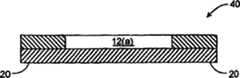
图1示出了根据本发明实施例的基片40。基片40可以支持半导体管芯封装中的半导体管芯(未示出)。Figure 1 shows a
基片40包括引线框架结构10和模制材料20。术语“引线框架结构”可表示由引线框架获得的结构。例如,可以通过蚀刻连续导电片以形成预定图案而形成引线框架。但是,如果使用模压,则引线框架初始就是通过系杆连接在一起的引线框架阵列中的许多引线框架之一。在制造半导体管芯封装的过程中,引线框架阵列会被切割以使引线框架与其它引线框架分开。作为该切割的结果,诸如源极引线和栅极引线的最终半导体管芯封装中的引线框架结构的一些部分会被电气地和机械地相互断开。因此,在本发明的实施例中,半导体管芯封装的引线框架结构会是连续的金属结构或者不连续的金属结构。
引线框架结构10包括管芯附着区域12。在该实例中,管芯附着区域12具有源极附着区域12(a)和栅极附着区域12(b)。当半导体管芯(未示出)位于管芯附着区域12上时,MOSFET(金属氧化物半导体场效应晶体管)的源极区和栅极区将分别耦合到源极附着区域12(a)和栅极附着区域12(b)。如果MOSFET是垂直MOSFET(以下详细描述),则MOSFET的漏极区将位于半导体管芯的相对侧。The
为了说明目的,上述基片实施例具有相互隔离的源极附着区域和栅极附着区域。但是,在其它实施例中,基片可以包括漏极附着区域取代源极附着区域和栅极附着区域或者除它们之外还包括漏极附着区域。如果半导体管芯包括垂直MOSFET,则MOSFET的含漏极区的表面将耦合到并靠近基片,同时在半导体管芯的另一侧上的源极区和栅极区将远离基片。For purposes of illustration, the substrate embodiments described above have source and gate attachment regions that are isolated from each other. However, in other embodiments, the substrate may include drain attachment regions instead of or in addition to the source and gate attachment regions. If the semiconductor die includes a vertical MOSFET, the surface of the MOSFET containing the drain region will be coupled to and close to the substrate, while the source and gate regions on the other side of the semiconductor die will be away from the substrate.
在该实例中,基片40具有含相应源极引线表面的5个源极引线14(a)-14(e)以及含栅极引线表面的栅极引线18。隐线示出模制材料20下面的连接,其将五个源极引线14(a)-14(e)耦合到源极附着区域12(a)。隐线还示出耦合到栅极附着区域12(b)的栅极引线18。栅极附着区域12(b)和源极附着区域12(a)相互电绝缘。In this example, the
引线框架结构10可以包括任何合适的材料,可以具有任何合适的形式,并可以具有任何合适的厚度。实例性的引线框架结构材料包括金属,诸如铜、铝、金等及其合金。引线框架结构还可以包括镀敷层,诸如金、铬、银、钯、镍等的镀敷层。引线框架结构10还可以具有任何合适的厚度,包括小于约1mm的厚度(例如,小于约0.5mm)。The
最终安装于基片40上的半导体管芯可以包括任何合适的半导体器件。合适的器件包括垂直功率晶体管。垂直功率晶体管包括VDMOS晶体管。VDMOS晶体管是具有通过扩散形成的两个或更多半导体区域的MOSFET。它具有源极区、漏极区和栅极。器件是垂直的,其源极区和漏极区位于半导体管芯的相对表面处。栅极是沟槽栅极结构或者平面栅极结构,并形成于同源极区相同的表面处。沟槽栅极结构是优选的,因为沟槽栅极结构更窄并比平面栅极结构占据更少的空间。在操作期间,VDMOS期间中从源极区到漏极区的电流基本垂直于管芯表面。The semiconductor die ultimately mounted on
模制材料20可以包括任何合适的材料。合适的模制材料包括联苯基材料,和多功能横向连接环氧树脂合成材料。如图1所示,引线14(a)-14(e),18没有侧向延伸向外延伸越过模制材料20,从而基片40可以被认为是“无引线”且包括该基片的封装可以被认为是“无引线”封装。
在某些实施例中,模制材料可以具有暗色(例如,黑色)。源极附着区域12(a)、源极引线14(a)-14(e)、栅极附着区域12(b)和栅极引线18可以包括具有与模制材料20的良好反差(contrast)的金属材料(例如,铜、铝)。良好反差使其更便于对准和沉积焊料或者将半导体管芯置于源极附着区域12、源极引线14(a)-14(e)、栅极附着区域12和栅极引线18。例如,改良的反差使机器更易于自动沉积焊料或自动拾取和放置半导体管芯于基片40上。这降低了形成有缺陷的半导体管芯封装的可能性。In some embodiments, the molding material may have a dark color (eg, black). Source attachment region 12(a), source leads 14(a)-14(e), gate attachment region 12(b), and
如上所述,管芯附着区域12包括源极附着区域12(a)和栅极附着区域12(b)。在所形成的半导体管芯封装中,MOSFET的源极区和栅极区可以位于封装中半导体管芯的相同侧处。半导体管芯中的源极区和栅极区可分别耦合到源极附着区域12(a)和栅极附着区域12(b)。可使用焊料将半导体管芯电气耦合到源极附着区域12(a)和栅极附着区域12(b)。As noted above, the die attach
如图1所示,栅极引线18的栅极引线表面和源极引线14(a)-14(e)的源极引线表面通过模制材料20暴露。同样,源极附着区域12(a)的表面和栅极附着区域12(b)的表面通过模制材料20暴露。在该实施例中,模制材料20的外表面以及源极附着区域12(a)、栅极附着区域12(b)、栅极引线18和源极引线14(a)-14(e)的暴露表面基本是共面的。As shown in FIG. 1 , the gate lead surface of
图2示出了使用图1所示的基片40的半导体管芯封装100。半导体管芯封装100包括管芯附着区域之上的半导体管芯50。焊料结构52(a)-52(e)(例如,焊料球)分别沉积于源极引线14(a)-14(e)上。另一个焊料结构56沉积于栅极引线18上。可以使用任何合适的工艺形成焊料结构52(a)-52(e)、56,包括丝网印刷、球附着、拾取和放置工艺等等。FIG. 2 shows a
在沉积焊料结构52(a)-52(e)、56和安装半导体管芯50于基片40上之后,半导体管芯封装100可以被翻转,随后安装到电路板上。After depositing solder structures 52(a)-52(e), 56 and mounting semiconductor die 50 on
图3和4分别示出根据本发明另一个实施例的基片和半导体管芯封装。在图1到4中,相同的标号表示相同的元件。图3和4中的实施例类似于图1和2中的元件,除了在图3和4所示的实施例中,存在更少的源极引线和相应焊料结构。与图1和2中的实施例相比,图3和4中基片和半导体管芯封装的面积更小。如通过图1-4的不同实施例所示,本发明的实施例可以具有任何合适数量的源极引线和漏极引线。3 and 4 illustrate a substrate and a semiconductor die package, respectively, according to another embodiment of the present invention. In Figs. 1 to 4, the same reference numerals denote the same elements. The embodiment in Figures 3 and 4 is similar to the elements in Figures 1 and 2, except that in the embodiment shown in Figures 3 and 4, there are fewer source leads and corresponding solder structures. Compared to the embodiments of FIGS. 1 and 2 , the substrate and semiconductor die package areas of FIGS. 3 and 4 are smaller. Embodiments of the invention may have any suitable number of source and drain leads, as shown by the different embodiments of FIGS. 1-4.
图5(a)示出了沿图1所示的线5(a)-5(a)获得的基片40的剖视图。图5(a)示出一基片,其中源极附着区域12(a)的相对主表面通过模制材料20暴露。在该实施例中,模制材料20的厚度可基本等于引线框架结构的厚度。引线框架结构的上表面和下表面的一些部分可通过模制材料20暴露。FIG. 5(a) shows a cross-sectional view of
图5(b)示出本发明的又一个实施例。在图5(b)中,示出了管芯附着区域的源极附着区域12(a),且模制材料20暴露源极附着区域12(a)。与图5(a)所示的实施例不同的是,模制材料20覆盖引线框架结构的侧表面和下表面。Figure 5(b) shows yet another embodiment of the present invention. In FIG. 5( b ), the source attach area 12 ( a ) of the die attach area is shown, and the
图5(a)所示的基片实施例比图5(b)所示的基片实施例更薄。例如,如果所形成的半导体管芯封装要用于较薄的装置中,诸如无线电话或膝上计算机,则这是期望的。The substrate embodiment shown in Figure 5(a) is thinner than the substrate embodiment shown in Figure 5(b). This is desirable, for example, if the formed semiconductor die package is to be used in thinner devices, such as wireless telephones or laptop computers.
图6示出沿线6-6获得的图1所示基片40的侧视图。如图所示,引线框架10包括源极附着区域12(a)和两个源极引线14(a),14(c)。模制材料20设置于引线框架10中的凹槽中。凹槽中的模制材料20可以帮助选择性地暴露源极引线14(a),14(b)。FIG. 6 shows a side view of
图7示出了沿线7-7获得的图2所示的半导体管芯封装100的侧剖视图。半导体管芯封装100包括通过焊料层48安装于引线框架结构10的源极附着区域12(a)和栅极附着区域12(b)上的半导体管芯50。该实施例中的焊料层48是不连续的,从而管芯50中的栅极和源极区不短路。焊料球52(e),56分别位于源极引线14(e)和栅极引线18上。模制材料20位于焊料球52(e),56和半导体管芯50之间的引线框架结构10中的凹槽中。模制材料20也位于源极附着区域12(a)和栅极附着区域12(b)之间以电气绝缘传递到半导体管芯50的栅极电流和源极电流。FIG. 7 shows a side cross-sectional view of the
图8示出根据本发明的另一个实施例的半导体管芯封装100。半导体管芯封装100包括基片40上的半导体管芯50。半导体管芯50可包括半导体管芯50的上表面处的源极区和栅极区,和其下表面处的漏极区。线路62例如可以耦合半导体管芯50中的源极区和源极引线60。另一线路(未示出)可耦合半导体管芯50的栅极区到栅极引线(未示出)。FIG. 8 illustrates a
密封材料66覆盖半导体管芯50和线路62以包含这些部件。在某些实施例中,密封材料66可以同模制材料20不同。可使用任何合适的密封材料。合适的密封材料包括联苯材料,以及多功能横向连接的环氧树脂合成物。Encapsulation material 66 covers semiconductor die 50 and wiring 62 to contain these components. In some embodiments, sealing material 66 may be different from
基片40包括引线框架12,它具有邻近于半导体管芯50的第一表面12-1和远离半导体管芯50的第二表面12-2。第一表面12-1的面积大于第二表面12-2的面积。通过减小第二表面的大小,封装100可以安装于电路板上的合适尺寸的导电焊盘上。
任何合适的工艺可形成减小面积的第二表面12-2。例如,光刻工艺可用于将光阻材料图案印制于诸如引线框架的金属结构上。随后,可以将合适的蚀刻剂用于蚀刻金属材料到合适深度,以形成引线框架结构的减小面积的第二表面12-2。光刻法和蚀刻工艺是本技术领域内已知的。Any suitable process may form reduced area second surface 12-2. For example, photolithography processes can be used to pattern photoresist material onto metal structures such as lead frames. Subsequently, a suitable etchant may be used to etch the metallic material to a suitable depth to form the reduced area second surface 12-2 of the lead frame structure. Photolithography and etching processes are known in the art.
与之前的实施例不同,图8所示的半导体管芯封装100可安装于电路板上而不颠倒。这样,当半导体管芯封装100安装于电路板上时,表面12-2比表面12-1更靠近电路板。Unlike the previous embodiments, the
根据本发明实施例的基片可用于纯粹电子器件之外的装置中。例如,本发明的实施例可用于光耦合器封装中。光耦合器封装包含至少一个光发射器装置,它通过光传输介质光耦合到光接收器装置。光发射器装置和光接收器装置可位于基片上(类似于上述的一些)。该设置允许信息从包含光发射器装置的一个电路传递到包含光接收器装置的另一个电路。在这两个电路之间维持高度电气绝缘。因为信息越过绝缘间隙而被光传播,所以该传送是单向的。例如,光接收器装置不能更改包含光发射器装置的电路的操作。该特点是有用的,因为例如发射器可以使用微处理器或逻辑门电路由低电压电路驱动,而输出光接收器装置可以是高电压DC或AC负载电路的一部分。光隔离还可以防止由相对对立的输出电路引起的对输入电路的损坏。合适的光耦合器装置的实例描述于美国专利申请No.09/944717,其提交于2001年8月31日,并被转让给本申请的相同受让人。该美国专利申请结合在此整体作为参考。Substrates according to embodiments of the present invention may be used in devices other than purely electronic devices. For example, embodiments of the present invention may be used in optocoupler packages. An optocoupler package contains at least one optical transmitter device that is optically coupled to an optical receiver device through an optical transmission medium. Optical transmitter devices and optical receiver devices may be located on a substrate (similar to some described above). This arrangement allows information to be passed from one circuit containing an optical transmitter device to another circuit containing an optical receiver device. A high degree of electrical isolation is maintained between these two circuits. Because the information is propagated by light across the insulating gap, the transmission is unidirectional. For example, an optical receiver device cannot alter the operation of a circuit containing an optical transmitter device. This feature is useful because, for example, the transmitter can be driven by a low voltage circuit using a microprocessor or logic gates, while the output optical receiver device can be part of a high voltage DC or AC load circuit. Optical isolation also prevents damage to input circuits caused by opposing output circuits. An example of a suitable optocoupler arrangement is described in US Patent Application No. 09/944717, filed August 31, 2001, and assigned to the same assignee as the present application. This US patent application is hereby incorporated by reference in its entirety.
图9示出了本发明的实施例中如何可以形成基片。在该实施例中,引线框架结构10(单独按引线框架的形式或者具有阵列中的其它引线框架)被粘着到带状结构18的粘合侧。随后,将该组合置于模具12的模具腔104中。模制化合物(以液体或半液体形式)随后被引入引线框架结构10之下的模制腔,如由标号96所表示的,且模制化合物向上通过并填充引线框架结构10中的缝隙25。一旦模化合物凝固,就可将带状结构38、引线框架10和模制化合物从模具12上移除。如果要形成如图5(a)中所示的基片,就可以在其凝固之前或之后从与带状结构38相对的引线框架结构10的侧部移除多余的模制化合物。接着,带状结构38可与所形成的基片分开。与带状结构38接触的金属表面通过凝固的模制化合物暴露。该过程可以是“带辅助单侧模制工艺”的实例。Figure 9 illustrates how a substrate may be formed in an embodiment of the invention. In this embodiment, the leadframe structure 10 (in the form of a leadframe alone or with other leadframes in an array) is adhered to the adhesive side of the
在另一个实施例中,代替使用模具,可以将模制材料丝网印刷入引线框架结构的缝隙中。例如,可以将引线框架结构置于表面(或带)上。可使用橡皮刮板或其它装置扩展模制材料进入引线框架结构的缝隙中。随后,如期望,可除去多余的模制化合物(例如,使用橡皮刮板)。模制材料可凝固且引线框架结构可与表面分开。之前与表面接触的引线框架结构的一些部分将没有模制材料并因此将通过凝固的模制材料暴露。此外,可进行去废料(dejunk)和去毛刺(deflash)工艺(本技术领域内已知)以除去多余的模制化合物。In another embodiment, instead of using a mold, the molding material can be screen printed into the gaps of the lead frame structure. For example, a leadframe structure may be placed on a surface (or tape). A squeegee or other device may be used to expand the molding material into the crevices of the lead frame structure. Subsequently, excess molding compound can be removed (eg, using a squeegee) if desired. The molding material can set and the lead frame structure can separate from the surface. Portions of the leadframe structure that were previously in contact with the surface will be free of molding material and thus will be exposed by the solidified molding material. Additionally, dejunk and deflash processes (known in the art) may be performed to remove excess molding compound.
在形成基片后,用于形成半导体封装的其余步骤可包括诸如焊料分配、焊料球附着、倒装芯片管芯附着,随后回流焊料球的步骤,从而可以将半导体管芯附着到基片上。After forming the substrate, the remaining steps for forming the semiconductor package may include steps such as solder dispensing, solder ball attachment, flip chip die attach, followed by reflowing the solder balls so that the semiconductor die can be attached to the substrate.
在将半导体管芯安装到引线框架之前或之后,可部分切割引线框架结构以隔离引线用于测试。例如,参考图1,源极引线14(1)-14(e)和栅极引线18可以是引线框架阵列内的单个引线框架结构10的一部分。最初,引线框架结构10可通过外框架状元件经由从每个引线14(a)-14(e),18向外延伸的“系杆”(未示出)机械地耦合在一起。在形成基片后,连到栅极引线18的系杆(未示出)可以被切割以使栅极引线18与元件引线14(a)-14(e)隔离。随后,在将其与其它基片分离之前电气测试该基片。The lead frame structure may be partially cut to isolate the leads for testing, either before or after mounting the semiconductor die to the lead frame. For example, referring to FIG. 1 , source leads 14 ( 1 )- 14 ( e ) and
如果基片通过测试,则半导体管芯封装阵列中的半导体管芯封装可按单数(singulation)工艺(例如,使用锯)相互分开。随后,本技术领域内已知的带和卷轴工艺可紧接着该单数工艺。有利地,在本发明的实施例中,不需要修整和形成模制的成形系数(form factor)专用工具。If the substrate passes the test, the semiconductor die packages in the array of semiconductor die packages may be separated from each other in a singulation process (eg, using a saw). The singular process may then be followed by a tape and reel process known in the art. Advantageously, in embodiments of the present invention, no special tooling is required for trimming and forming the molded form factor.
本发明的实施例具有大量其它优点。首先,如上所述,在本发明的实施例中,在基片中使用引线框架结构。引线框架结构是廉价且便于制造的。因此,根据本发明的实施例的基片可以更廉价地制成。例如,与陶瓷金属化基片相比,根据本发明实施例制成的基片的成本可以降低约70%或以上。其次,根据本发明实施例的基片具有模制材料和引线框架的暴露区域之间的高反差。如以上进一步说明的,这导致更少的缺陷。第三,本发明的实施例可制成得比常规半导体管芯封装和基片更薄。相比现有技术的封装的当前状态,本发明实施例的封装尺寸可降低至少20%。例如,根据本发明实施例的半导体管芯封装的厚度可以在约0.5mm(或更小)的数量级上。第四,在本发明的实施例中,模制过程是与成形系数无关的,因为它用于构建基片,且不需要用于完全密封半导体管芯。第五,可以使用已知的“倒装芯片”技术安装本发明实施例的基片和封装。第六,在本发明的实施例中,可以在引线框架结构中蚀刻精细的几何形状,从而封装引线和管芯附着表面可按需要而定制。第七,根据本发明实施例的基片是机械刚性的,但仍足够柔性以便在高度自动化的设备中运用。Embodiments of the invention have numerous other advantages. First, as described above, in the embodiment of the present invention, a lead frame structure is used in the substrate. Lead frame structures are cheap and easy to manufacture. Therefore, substrates according to embodiments of the present invention can be made more inexpensively. For example, the cost of substrates made according to embodiments of the present invention can be reduced by about 70% or more compared to ceramic metallized substrates. Second, substrates according to embodiments of the present invention have high contrast between the molding material and the exposed areas of the lead frame. As explained further above, this results in fewer defects. Third, embodiments of the present invention can be made thinner than conventional semiconductor die packages and substrates. Compared to the current state of the art packaging, embodiments of the present invention may reduce package size by at least 20%. For example, the thickness of a semiconductor die package according to an embodiment of the invention may be on the order of about 0.5 mm (or less). Fourth, in embodiments of the present invention, the molding process is form factor independent since it is used to build the substrate and does not need to be used to fully encapsulate the semiconductor die. Fifth, the substrate and package of embodiments of the present invention can be mounted using known "flip-chip" techniques. Sixth, in embodiments of the present invention, fine geometry can be etched into the lead frame structure so that package leads and die attach surfaces can be customized as desired. Seventh, substrates according to embodiments of the present invention are mechanically rigid, yet flexible enough to be used in highly automated equipment.
此外,在本发明的实施例中,可以预先模制引线框架以形成基片,随后(用管芯)封装该基片以形成封装。有利地,可以蚀刻或印制非常薄的引线框架。例如,可以采用约4密耳厚的铜箔,将其冲压或蚀刻为所需图案,随后将其模制入约6到8密耳厚的基片。现在,可在常规装配设备(例如,倒装芯片接合器)中方便地运用所形成的基片。与常规镀敷工艺相比,本发明的实施例减少了处理时间并提升了制造的方便性。例如,铜按约4-8微米/分钟的速度镀敷。为了获得4密耳厚的铜轨迹一般将花费30到40分钟。本发明的实施例花费更少的时间来制造,因为预先形成的引线框架可用于形成基片。Furthermore, in embodiments of the present invention, a lead frame may be pre-molded to form a substrate, which is subsequently packaged (with a die) to form a package. Advantageously, very thin leadframes can be etched or printed. For example, copper foil about 4 mils thick can be used, which is stamped or etched into the desired pattern and then molded into a substrate about 6 to 8 mils thick. The formed substrates can now be conveniently employed in conventional assembly equipment (eg, flip chip bonders). Embodiments of the present invention reduce processing time and improve ease of manufacture compared to conventional plating processes. For example, copper is plated at a rate of about 4-8 microns/minute. It will typically take 30 to 40 minutes to obtain a 4 mil thick copper trace. Embodiments of the present invention take less time to manufacture because pre-formed lead frames can be used to form the substrate.
这里所采用的术语和表达用于描述而非限制性的,且这种术语和表达的使用不旨在排出所示和描述的等效物或其部分,可以理解,各种修改都落在所要求的本发明的范围之内。此外,本发明的任何实施例的任一个或多个特点可以与本发明的任何其它实施例的任一个或多个其它特点组合,而不背离本发明的范围。例如,可以理解,图5(b)所示的类型的基片可用于图2和4所示的半导体管芯封装中。The terms and expressions employed herein are for the purpose of description rather than limitation, and the use of such terms and expressions is not intended to exclude equivalents or parts thereof shown and described, and it is understood that various modifications fall within the scope of the present invention. within the scope of the claimed invention. Furthermore, any one or more features of any embodiment of the invention may be combined with any one or more other features of any other embodiment of the invention without departing from the scope of the invention. For example, it is understood that a substrate of the type shown in FIG. 5(b) may be used in the semiconductor die package shown in FIGS. 2 and 4 .
Claims (20)
Translated fromChineseApplications Claiming Priority (3)
| Application Number | Priority Date | Filing Date | Title |
|---|---|---|---|
| US10/233,248 | 2002-08-30 | ||
| US10/233,248US7061077B2 (en) | 2002-08-30 | 2002-08-30 | Substrate based unmolded package including lead frame structure and semiconductor die |
| PCT/US2003/023864WO2004021400A2 (en) | 2002-08-30 | 2003-07-30 | Substrate based unmolded package |
Related Child Applications (1)
| Application Number | Title | Priority Date | Filing Date |
|---|---|---|---|
| CN2009101747995ADivisionCN101685811B (en) | 2002-08-30 | 2003-07-30 | Substrate based unmolded package |
Publications (2)
| Publication Number | Publication Date |
|---|---|
| CN1679162Atrue CN1679162A (en) | 2005-10-05 |
| CN1679162B CN1679162B (en) | 2010-06-02 |
Family
ID=31977195
Family Applications (2)
| Application Number | Title | Priority Date | Filing Date |
|---|---|---|---|
| CN038203995AExpired - Fee RelatedCN1679162B (en) | 2002-08-30 | 2003-07-30 | Substrate-based unmolded package and method of forming the same |
| CN2009101747995AExpired - Fee RelatedCN101685811B (en) | 2002-08-30 | 2003-07-30 | Substrate based unmolded package |
Family Applications After (1)
| Application Number | Title | Priority Date | Filing Date |
|---|---|---|---|
| CN2009101747995AExpired - Fee RelatedCN101685811B (en) | 2002-08-30 | 2003-07-30 | Substrate based unmolded package |
Country Status (9)
| Country | Link |
|---|---|
| US (6) | US7061077B2 (en) |
| JP (2) | JP4634146B2 (en) |
| KR (1) | KR101037997B1 (en) |
| CN (2) | CN1679162B (en) |
| AU (1) | AU2003257046A1 (en) |
| DE (1) | DE10393164T5 (en) |
| MY (1) | MY149851A (en) |
| TW (2) | TWI267176B (en) |
| WO (1) | WO2004021400A2 (en) |
Cited By (4)
| Publication number | Priority date | Publication date | Assignee | Title |
|---|---|---|---|---|
| CN102543909A (en)* | 2012-03-01 | 2012-07-04 | 日月光半导体制造股份有限公司 | Irregular-shaped packaging structure and manufacturing method thereof |
| CN101556946B (en)* | 2008-04-07 | 2012-11-21 | 半导体元件工业有限责任公司 | Method of forming a semiconductor package and structure thereof |
| US8525192B2 (en) | 2008-01-09 | 2013-09-03 | Fairchild Semiconductor Corporation | Die package including substrate with molded device |
| CN105244296A (en)* | 2014-07-07 | 2016-01-13 | 英飞凌科技股份有限公司 | Extended contact area for leadframe strip testing |
Families Citing this family (68)
| Publication number | Priority date | Publication date | Assignee | Title |
|---|---|---|---|---|
| US6753605B2 (en) | 2000-12-04 | 2004-06-22 | Fairchild Semiconductor Corporation | Passivation scheme for bumped wafers |
| US6469384B2 (en)* | 2001-02-01 | 2002-10-22 | Fairchild Semiconductor Corporation | Unmolded package for a semiconductor device |
| US7122884B2 (en)* | 2002-04-16 | 2006-10-17 | Fairchild Semiconductor Corporation | Robust leaded molded packages and methods for forming the same |
| US7061077B2 (en)* | 2002-08-30 | 2006-06-13 | Fairchild Semiconductor Corporation | Substrate based unmolded package including lead frame structure and semiconductor die |
| US7217594B2 (en)* | 2003-02-11 | 2007-05-15 | Fairchild Semiconductor Corporation | Alternative flip chip in leaded molded package design and method for manufacture |
| US20060003483A1 (en)* | 2003-07-07 | 2006-01-05 | Wolff Larry L | Optoelectronic packaging with embedded window |
| US6919625B2 (en)* | 2003-07-10 | 2005-07-19 | General Semiconductor, Inc. | Surface mount multichip devices |
| TWI254437B (en)* | 2003-12-31 | 2006-05-01 | Advanced Semiconductor Eng | Leadless package |
| US7196313B2 (en)* | 2004-04-02 | 2007-03-27 | Fairchild Semiconductor Corporation | Surface mount multi-channel optocoupler |
| US7256479B2 (en)* | 2005-01-13 | 2007-08-14 | Fairchild Semiconductor Corporation | Method to manufacture a universal footprint for a package with exposed chip |
| JP2006210777A (en)* | 2005-01-31 | 2006-08-10 | Nec Electronics Corp | Semiconductor device |
| US7226821B2 (en)* | 2005-06-24 | 2007-06-05 | Cardiac Pacemakers, Inc. | Flip chip die assembly using thin flexible substrates |
| WO2007005263A2 (en)* | 2005-06-30 | 2007-01-11 | Fairchild Semiconductor Corporation | Semiconductor die package and method for making the same |
| US7285849B2 (en)* | 2005-11-18 | 2007-10-23 | Fairchild Semiconductor Corporation | Semiconductor die package using leadframe and clip and method of manufacturing |
| US20090057852A1 (en)* | 2007-08-27 | 2009-03-05 | Madrid Ruben P | Thermally enhanced thin semiconductor package |
| US7371616B2 (en)* | 2006-01-05 | 2008-05-13 | Fairchild Semiconductor Corporation | Clipless and wireless semiconductor die package and method for making the same |
| US20070164428A1 (en)* | 2006-01-18 | 2007-07-19 | Alan Elbanhawy | High power module with open frame package |
| US7868432B2 (en)* | 2006-02-13 | 2011-01-11 | Fairchild Semiconductor Corporation | Multi-chip module for battery power control |
| US7768075B2 (en)* | 2006-04-06 | 2010-08-03 | Fairchild Semiconductor Corporation | Semiconductor die packages using thin dies and metal substrates |
| US7618896B2 (en) | 2006-04-24 | 2009-11-17 | Fairchild Semiconductor Corporation | Semiconductor die package including multiple dies and a common node structure |
| US7656024B2 (en) | 2006-06-30 | 2010-02-02 | Fairchild Semiconductor Corporation | Chip module for complete power train |
| US7564124B2 (en) | 2006-08-29 | 2009-07-21 | Fairchild Semiconductor Corporation | Semiconductor die package including stacked dice and heat sink structures |
| US7927923B2 (en)* | 2006-09-25 | 2011-04-19 | Micron Technology, Inc. | Method and apparatus for directing molding compound flow and resulting semiconductor device packages |
| US7768105B2 (en) | 2007-01-24 | 2010-08-03 | Fairchild Semiconductor Corporation | Pre-molded clip structure |
| US8106501B2 (en)* | 2008-12-12 | 2012-01-31 | Fairchild Semiconductor Corporation | Semiconductor die package including low stress configuration |
| US7821116B2 (en)* | 2007-02-05 | 2010-10-26 | Fairchild Semiconductor Corporation | Semiconductor die package including leadframe with die attach pad with folded edge |
| US8159828B2 (en)* | 2007-02-23 | 2012-04-17 | Alpha & Omega Semiconductor, Inc. | Low profile flip chip power module and method of making |
| KR101391925B1 (en)* | 2007-02-28 | 2014-05-07 | 페어차일드코리아반도체 주식회사 | Semiconductor package and semiconductor package mold for fabricating the same |
| KR101489325B1 (en) | 2007-03-12 | 2015-02-06 | 페어차일드코리아반도체 주식회사 | Flip-chip type stacked power module and method of manufacturing the power module |
| US7659531B2 (en)* | 2007-04-13 | 2010-02-09 | Fairchild Semiconductor Corporation | Optical coupler package |
| US7683463B2 (en)* | 2007-04-19 | 2010-03-23 | Fairchild Semiconductor Corporation | Etched leadframe structure including recesses |
| US7902657B2 (en)* | 2007-08-28 | 2011-03-08 | Fairchild Semiconductor Corporation | Self locking and aligning clip structure for semiconductor die package |
| US7737548B2 (en) | 2007-08-29 | 2010-06-15 | Fairchild Semiconductor Corporation | Semiconductor die package including heat sinks |
| US20090057855A1 (en)* | 2007-08-30 | 2009-03-05 | Maria Clemens Quinones | Semiconductor die package including stand off structures |
| US7768123B2 (en)* | 2007-09-26 | 2010-08-03 | Fairchild Semiconductor Corporation | Stacked dual-die packages, methods of making, and systems incorporating said packages |
| US7727813B2 (en) | 2007-11-26 | 2010-06-01 | Infineon Technologies Ag | Method for making a device including placing a semiconductor chip on a substrate |
| US20090140266A1 (en)* | 2007-11-30 | 2009-06-04 | Yong Liu | Package including oriented devices |
| US7589338B2 (en)* | 2007-11-30 | 2009-09-15 | Fairchild Semiconductor Corporation | Semiconductor die packages suitable for optoelectronic applications having clip attach structures for angled mounting of dice |
| KR20090062612A (en)* | 2007-12-13 | 2009-06-17 | 페어차일드코리아반도체 주식회사 | Multi-chip package |
| US7781872B2 (en)* | 2007-12-19 | 2010-08-24 | Fairchild Semiconductor Corporation | Package with multiple dies |
| US7791084B2 (en) | 2008-01-09 | 2010-09-07 | Fairchild Semiconductor Corporation | Package with overlapping devices |
| US7626249B2 (en)* | 2008-01-10 | 2009-12-01 | Fairchild Semiconductor Corporation | Flex clip connector for semiconductor device |
| KR101463074B1 (en)* | 2008-01-10 | 2014-11-21 | 페어차일드코리아반도체 주식회사 | Leadless package |
| US20090194857A1 (en)* | 2008-02-01 | 2009-08-06 | Yong Liu | Thin Compact Semiconductor Die Packages Suitable for Smart-Power Modules, Methods of Making the Same, and Systems Using the Same |
| US20090194856A1 (en)* | 2008-02-06 | 2009-08-06 | Gomez Jocel P | Molded package assembly |
| KR101524545B1 (en)* | 2008-02-28 | 2015-06-01 | 페어차일드코리아반도체 주식회사 | Power device package and the method of fabricating the same |
| US7768108B2 (en)* | 2008-03-12 | 2010-08-03 | Fairchild Semiconductor Corporation | Semiconductor die package including embedded flip chip |
| US8018054B2 (en)* | 2008-03-12 | 2011-09-13 | Fairchild Semiconductor Corporation | Semiconductor die package including multiple semiconductor dice |
| US7893548B2 (en)* | 2008-03-24 | 2011-02-22 | Fairchild Semiconductor Corporation | SiP substrate |
| KR101519062B1 (en)* | 2008-03-31 | 2015-05-11 | 페어차일드코리아반도체 주식회사 | Semiconductor Device Package |
| US20090278241A1 (en)* | 2008-05-08 | 2009-11-12 | Yong Liu | Semiconductor die package including die stacked on premolded substrate including die |
| US7855439B2 (en)* | 2008-08-28 | 2010-12-21 | Fairchild Semiconductor Corporation | Molded ultra thin semiconductor die packages, systems using the same, and methods of making the same |
| US7829988B2 (en)* | 2008-09-22 | 2010-11-09 | Fairchild Semiconductor Corporation | Stacking quad pre-molded component packages, systems using the same, and methods of making the same |
| US8314499B2 (en)* | 2008-11-14 | 2012-11-20 | Fairchild Semiconductor Corporation | Flexible and stackable semiconductor die packages having thin patterned conductive layers |
| US8193618B2 (en) | 2008-12-12 | 2012-06-05 | Fairchild Semiconductor Corporation | Semiconductor die package with clip interconnection |
| US7816784B2 (en) | 2008-12-17 | 2010-10-19 | Fairchild Semiconductor Corporation | Power quad flat no-lead semiconductor die packages with isolated heat sink for high-voltage, high-power applications, systems using the same, and methods of making the same |
| US7973393B2 (en) | 2009-02-04 | 2011-07-05 | Fairchild Semiconductor Corporation | Stacked micro optocouplers and methods of making the same |
| US8222718B2 (en)* | 2009-02-05 | 2012-07-17 | Fairchild Semiconductor Corporation | Semiconductor die package and method for making the same |
| JP4985810B2 (en)* | 2010-03-23 | 2012-07-25 | サンケン電気株式会社 | Semiconductor device |
| US8655481B2 (en)* | 2010-04-09 | 2014-02-18 | Victor Shi-Yueh Sheu | IMR (in-mold roller or in-mold release)/IMF (in-mold forming) making method using a digital printer printing and pre-forming technique |
| US8252631B1 (en)* | 2011-04-28 | 2012-08-28 | Freescale Semiconductor, Inc. | Method and apparatus for integrated circuit packages using materials with low melting point |
| US8421204B2 (en) | 2011-05-18 | 2013-04-16 | Fairchild Semiconductor Corporation | Embedded semiconductor power modules and packages |
| US20130082365A1 (en) | 2011-10-03 | 2013-04-04 | International Business Machines Corporation | Interposer for ESD, EMI, and EMC |
| US9691745B2 (en)* | 2013-06-26 | 2017-06-27 | Taiwan Semiconductor Manufacturing Co., Ltd. | Bonding structure for forming a package on package (PoP) structure and method for forming the same |
| US9252076B2 (en) | 2013-08-07 | 2016-02-02 | Taiwan Semiconductor Manufacturing Company, Ltd. | 3D packages and methods for forming the same |
| US20180261535A1 (en)* | 2014-12-15 | 2018-09-13 | Bridge Semiconductor Corp. | Method of making wiring board with dual routing circuitries integrated with leadframe |
| DE102015215497B4 (en) | 2015-08-13 | 2024-07-18 | Audi Ag | Fuel cell stack with variable segmentation as well as fuel cell system and vehicle with such a |
| US11393743B2 (en)* | 2019-12-18 | 2022-07-19 | Infineon Technologies Ag | Semiconductor assembly with conductive frame for I/O standoff and thermal dissipation |
Family Cites Families (70)
| Publication number | Priority date | Publication date | Assignee | Title |
|---|---|---|---|---|
| US3982317A (en) | 1975-07-31 | 1976-09-28 | Sprague Electric Company | Method for continuous assembly and batch molding of transistor packages |
| US4789709A (en)* | 1985-05-02 | 1988-12-06 | Sumitomo Chemical Company, Limited | Process for the production of heat resistant thermoplastic copolymer |
| NL8602091A (en) | 1986-08-18 | 1988-03-16 | Philips Nv | IMAGE RECORDING DEVICE EQUIPPED WITH A SOLID IMAGE RECORDER AND AN ELECTRONIC SHUTTER. |
| US5164218A (en) | 1989-05-12 | 1992-11-17 | Nippon Soken, Inc. | Semiconductor device and a method for producing the same |
| JPH03108744A (en) | 1989-09-22 | 1991-05-08 | Toshiba Corp | Resin-sealed semiconductor device |
| US5172214A (en) | 1991-02-06 | 1992-12-15 | Motorola, Inc. | Leadless semiconductor device and method for making the same |
| US5448450A (en) | 1991-08-15 | 1995-09-05 | Staktek Corporation | Lead-on-chip integrated circuit apparatus |
| US5307272A (en)* | 1991-08-19 | 1994-04-26 | The United States Of America As Represented By The United States Department Of Energy | Minefield reconnaissance and detector system |
| JP3016658B2 (en) | 1992-04-28 | 2000-03-06 | ローム株式会社 | Lead frame, semiconductor device and method of manufacturing the same |
| JPH0732225B2 (en)* | 1992-10-14 | 1995-04-10 | 富士機工電子株式会社 | Method of forming pin holding portion on lead frame and method of forming dam portion |
| KR100280762B1 (en)* | 1992-11-03 | 2001-03-02 | 비센트 비.인그라시아 | Thermally Reinforced Semiconductor Devices Having Exposed Backsides and Methods of Manufacturing the Same |
| JP3254865B2 (en) | 1993-12-17 | 2002-02-12 | ソニー株式会社 | Camera device |
| FR2721694B1 (en)* | 1994-06-22 | 1996-07-19 | Snecma | Cooling of the take-off injector of a combustion chamber with two heads. |
| JPH08250641A (en)* | 1995-03-09 | 1996-09-27 | Fujitsu Ltd | Semiconductor device and manufacturing method thereof |
| US5789809A (en) | 1995-08-22 | 1998-08-04 | National Semiconductor Corporation | Thermally enhanced micro-ball grid array package |
| JP3549294B2 (en)* | 1995-08-23 | 2004-08-04 | 新光電気工業株式会社 | Semiconductor device and its mounting structure |
| US5765208A (en)* | 1995-09-29 | 1998-06-09 | Motorola, Inc. | Method of speculatively executing store instructions prior to performing snoop operations |
| US5637916A (en) | 1996-02-02 | 1997-06-10 | National Semiconductor Corporation | Carrier based IC packaging arrangement |
| JPH09321173A (en)* | 1996-05-27 | 1997-12-12 | Shinko Electric Ind Co Ltd | Semiconductor device package, semiconductor device and their manufacture |
| JPH09312355A (en) | 1996-05-21 | 1997-12-02 | Shinko Electric Ind Co Ltd | Semiconductor device and its manufacture |
| US5847458A (en)* | 1996-05-21 | 1998-12-08 | Shinko Electric Industries Co., Ltd. | Semiconductor package and device having heads coupled with insulating material |
| KR19980044247A (en) | 1996-12-06 | 1998-09-05 | 황인길 | Molding method of semiconductor package |
| KR100258852B1 (en) | 1996-12-19 | 2000-06-15 | 김영환 | Manufacturing method of semiconductor package |
| US6545384B1 (en)* | 1997-02-07 | 2003-04-08 | Sri International | Electroactive polymer devices |
| KR100214555B1 (en) | 1997-02-14 | 1999-08-02 | 구본준 | Manufacturing method of semiconductor package |
| JP2000049184A (en)* | 1998-05-27 | 2000-02-18 | Hitachi Ltd | Semiconductor device and method of manufacturing the same |
| US6249041B1 (en)* | 1998-06-02 | 2001-06-19 | Siliconix Incorporated | IC chip package with directly connected leads |
| US6229200B1 (en) | 1998-06-10 | 2001-05-08 | Asat Limited | Saw-singulated leadless plastic chip carrier |
| JP2000003988A (en) | 1998-06-15 | 2000-01-07 | Sony Corp | Lead frame and semiconductor device |
| US6143981A (en) | 1998-06-24 | 2000-11-07 | Amkor Technology, Inc. | Plastic integrated circuit package and method and leadframe for making the package |
| US6133634A (en) | 1998-08-05 | 2000-10-17 | Fairchild Semiconductor Corporation | High performance flip chip package |
| JP2000138107A (en)* | 1998-11-04 | 2000-05-16 | Mitsubishi Materials Corp | Semiconductor surge absorber |
| JP4260263B2 (en)* | 1999-01-28 | 2009-04-30 | 株式会社ルネサステクノロジ | Semiconductor device |
| JP3871486B2 (en)* | 1999-02-17 | 2007-01-24 | 株式会社ルネサステクノロジ | Semiconductor device |
| JP2000294580A (en) | 1999-04-12 | 2000-10-20 | Nitto Denko Corp | Resin sealing method for semiconductor chip and adhesive tape for sticking lead frame etc. |
| JP3686287B2 (en)* | 1999-07-14 | 2005-08-24 | 株式会社ルネサステクノロジ | Manufacturing method of semiconductor device |
| US6384487B1 (en)* | 1999-12-06 | 2002-05-07 | Micron Technology, Inc. | Bow resistant plastic semiconductor package and method of fabrication |
| US6720642B1 (en) | 1999-12-16 | 2004-04-13 | Fairchild Semiconductor Corporation | Flip chip in leaded molded package and method of manufacture thereof |
| JP3420153B2 (en)* | 2000-01-24 | 2003-06-23 | Necエレクトロニクス株式会社 | Semiconductor device and manufacturing method thereof |
| DE10103428A1 (en)* | 2000-02-23 | 2001-08-30 | Basf Ag | Composition containing polyacrylate to be processed from melt and phosphite stabilizer is useful as hot-melt adhesive, e.g. for production of self-adhesive labels, adhesive tape or protective film |
| US6384472B1 (en)* | 2000-03-24 | 2002-05-07 | Siliconware Precision Industries Co., Ltd | Leadless image sensor package structure and method for making the same |
| US6624522B2 (en)* | 2000-04-04 | 2003-09-23 | International Rectifier Corporation | Chip scale surface mounted device and process of manufacture |
| US6870254B1 (en)* | 2000-04-13 | 2005-03-22 | Fairchild Semiconductor Corporation | Flip clip attach and copper clip attach on MOSFET device |
| US6355502B1 (en) | 2000-04-25 | 2002-03-12 | National Science Council | Semiconductor package and method for making the same |
| US6661082B1 (en) | 2000-07-19 | 2003-12-09 | Fairchild Semiconductor Corporation | Flip chip substrate design |
| JP3639515B2 (en)* | 2000-09-04 | 2005-04-20 | 三洋電機株式会社 | Method for manufacturing MOSFET mounting structure |
| US6545364B2 (en) | 2000-09-04 | 2003-04-08 | Sanyo Electric Co., Ltd. | Circuit device and method of manufacturing the same |
| JP3745213B2 (en)* | 2000-09-27 | 2006-02-15 | 株式会社東芝 | Semiconductor device and manufacturing method thereof |
| TW458377U (en)* | 2000-11-23 | 2001-10-01 | Siliconware Precision Industries Co Ltd | Sensor structure of quad flat package without external leads |
| US6798044B2 (en) | 2000-12-04 | 2004-09-28 | Fairchild Semiconductor Corporation | Flip chip in leaded molded package with two dies |
| US6753605B2 (en) | 2000-12-04 | 2004-06-22 | Fairchild Semiconductor Corporation | Passivation scheme for bumped wafers |
| KR20020045674A (en) | 2000-12-09 | 2002-06-20 | 윤종용 | Manufacturing method for dual die package using tape |
| US6864423B2 (en) | 2000-12-15 | 2005-03-08 | Semiconductor Component Industries, L.L.C. | Bump chip lead frame and package |
| JP2002203957A (en)* | 2000-12-28 | 2002-07-19 | Rohm Co Ltd | Transistor |
| JP2002217416A (en)* | 2001-01-16 | 2002-08-02 | Hitachi Ltd | Semiconductor device |
| US6469384B2 (en) | 2001-02-01 | 2002-10-22 | Fairchild Semiconductor Corporation | Unmolded package for a semiconductor device |
| KR100704311B1 (en) | 2001-02-05 | 2007-04-05 | 삼성전자주식회사 | Internal lead exposed semiconductor chip package and its manufacturing method |
| US6731002B2 (en)* | 2001-05-04 | 2004-05-04 | Ixys Corporation | High frequency power device with a plastic molded package and direct bonded substrate |
| US6893901B2 (en)* | 2001-05-14 | 2005-05-17 | Fairchild Semiconductor Corporation | Carrier with metal bumps for semiconductor die packages |
| US7057273B2 (en) | 2001-05-15 | 2006-06-06 | Gem Services, Inc. | Surface mount package |
| US6524886B2 (en) | 2001-05-24 | 2003-02-25 | Advanced Semiconductor Engineering Inc. | Method of making leadless semiconductor package |
| US6679888B2 (en)* | 2001-05-29 | 2004-01-20 | Synthes | Femur lever |
| US6633030B2 (en) | 2001-08-31 | 2003-10-14 | Fiarchild Semiconductor | Surface mountable optocoupler package |
| US6461900B1 (en)* | 2001-10-18 | 2002-10-08 | Chartered Semiconductor Manufacturing Ltd. | Method to form a self-aligned CMOS inverter using vertical device integration |
| US6630726B1 (en) | 2001-11-07 | 2003-10-07 | Amkor Technology, Inc. | Power semiconductor package with strap |
| US6737750B1 (en) | 2001-12-07 | 2004-05-18 | Amkor Technology, Inc. | Structures for improving heat dissipation in stacked semiconductor packages |
| US6650015B2 (en)* | 2002-02-05 | 2003-11-18 | Siliconware Precision Industries Co., Ltd. | Cavity-down ball grid array package with semiconductor chip solder ball |
| US7061077B2 (en)* | 2002-08-30 | 2006-06-13 | Fairchild Semiconductor Corporation | Substrate based unmolded package including lead frame structure and semiconductor die |
| US6777800B2 (en)* | 2002-09-30 | 2004-08-17 | Fairchild Semiconductor Corporation | Semiconductor die package including drain clip |
| US7196313B2 (en) | 2004-04-02 | 2007-03-27 | Fairchild Semiconductor Corporation | Surface mount multi-channel optocoupler |
- 2002
- 2002-08-30USUS10/233,248patent/US7061077B2/ennot_activeExpired - Lifetime
- 2003
- 2003-07-30CNCN038203995Apatent/CN1679162B/ennot_activeExpired - Fee Related
- 2003-07-30WOPCT/US2003/023864patent/WO2004021400A2/enactiveApplication Filing
- 2003-07-30DEDE10393164Tpatent/DE10393164T5/ennot_activeCeased
- 2003-07-30CNCN2009101747995Apatent/CN101685811B/ennot_activeExpired - Fee Related
- 2003-07-30KRKR1020057001655Apatent/KR101037997B1/ennot_activeExpired - Fee Related
- 2003-07-30JPJP2004532833Apatent/JP4634146B2/ennot_activeExpired - Fee Related
- 2003-07-30AUAU2003257046Apatent/AU2003257046A1/ennot_activeAbandoned
- 2003-08-13TWTW094126031Apatent/TWI267176B/ennot_activeIP Right Cessation
- 2003-08-13TWTW092122242Apatent/TWI266393B/ennot_activeIP Right Cessation
- 2003-08-28MYMYPI20033260Apatent/MY149851A/enunknown
- 2004
- 2004-05-06USUS10/841,656patent/US7439613B2/ennot_activeExpired - Fee Related
- 2005
- 2005-07-12USUS11/180,367patent/US8541890B2/enactiveActive
- 2005-07-12USUS11/180,405patent/US7504281B2/ennot_activeExpired - Lifetime
- 2008
- 2008-05-09USUS12/118,222patent/US7682877B2/ennot_activeExpired - Lifetime
- 2009
- 2009-01-23USUS12/358,654patent/US7790513B2/ennot_activeExpired - Fee Related
- 2010
- 2010-09-03JPJP2010197828Apatent/JP2011018924A/enactivePending
Cited By (6)
| Publication number | Priority date | Publication date | Assignee | Title |
|---|---|---|---|---|
| US8525192B2 (en) | 2008-01-09 | 2013-09-03 | Fairchild Semiconductor Corporation | Die package including substrate with molded device |
| CN101556946B (en)* | 2008-04-07 | 2012-11-21 | 半导体元件工业有限责任公司 | Method of forming a semiconductor package and structure thereof |
| CN102543909A (en)* | 2012-03-01 | 2012-07-04 | 日月光半导体制造股份有限公司 | Irregular-shaped packaging structure and manufacturing method thereof |
| CN102543909B (en)* | 2012-03-01 | 2016-08-17 | 日月光半导体制造股份有限公司 | Irregular-shaped packaging structure and manufacturing method thereof |
| CN105244296A (en)* | 2014-07-07 | 2016-01-13 | 英飞凌科技股份有限公司 | Extended contact area for leadframe strip testing |
| CN105244296B (en)* | 2014-07-07 | 2018-06-26 | 英飞凌科技股份有限公司 | For the extension contact area of lead moulding test |
Also Published As
| Publication number | Publication date |
|---|---|
| US8541890B2 (en) | 2013-09-24 |
| US20080213946A1 (en) | 2008-09-04 |
| AU2003257046A1 (en) | 2004-03-19 |
| DE10393164T5 (en) | 2005-08-18 |
| JP2005537664A (en) | 2005-12-08 |
| JP2011018924A (en) | 2011-01-27 |
| TW200539401A (en) | 2005-12-01 |
| AU2003257046A8 (en) | 2004-03-19 |
| MY149851A (en) | 2013-10-31 |
| US7504281B2 (en) | 2009-03-17 |
| KR101037997B1 (en) | 2011-05-30 |
| WO2004021400A2 (en) | 2004-03-11 |
| US20060003492A1 (en) | 2006-01-05 |
| JP4634146B2 (en) | 2011-02-16 |
| US20090130802A1 (en) | 2009-05-21 |
| CN101685811B (en) | 2012-12-05 |
| TW200408084A (en) | 2004-05-16 |
| CN1679162B (en) | 2010-06-02 |
| CN101685811A (en) | 2010-03-31 |
| US7439613B2 (en) | 2008-10-21 |
| US7061077B2 (en) | 2006-06-13 |
| US20040041242A1 (en) | 2004-03-04 |
| US20040207052A1 (en) | 2004-10-21 |
| KR20050039833A (en) | 2005-04-29 |
| US7682877B2 (en) | 2010-03-23 |
| US7790513B2 (en) | 2010-09-07 |
| TWI267176B (en) | 2006-11-21 |
| US20060006550A1 (en) | 2006-01-12 |
| TWI266393B (en) | 2006-11-11 |
| WO2004021400A3 (en) | 2004-06-17 |
Similar Documents
| Publication | Publication Date | Title |
|---|---|---|
| CN1679162A (en) | Substrate based unmolded package | |
| US20250149412A1 (en) | Leadless semiconductor packages, leadframes therefor, and methods of making | |
| US8163601B2 (en) | Chip-exposed semiconductor device and its packaging method | |
| DE102011053871B4 (en) | Multichip semiconductor packages and their assembly | |
| US6911353B2 (en) | Semiconductor device and method of manufacturing same | |
| TWI405274B (en) | Clipless and wireless semiconductor die package and method for making the same | |
| EP1179844A2 (en) | Semiconductor packaging | |
| CN1571151A (en) | Double gauge lead frame | |
| CN1914719A (en) | Flipchip QFN package and method therefor | |
| US5299091A (en) | Packaged semiconductor device having heat dissipation/electrical connection bumps and method of manufacturing same | |
| US12300583B2 (en) | Concealed gate terminal semiconductor packages and related methods | |
| US11721654B2 (en) | Ultra-thin multichip power devices | |
| CN103579029B (en) | Package structure and method for manufacturing the same | |
| US20060001816A1 (en) | IPS-LCD device having optical compensation films | |
| US20250070071A1 (en) | Semiconductor device and semiconductor device fabrication method | |
| US20240096725A1 (en) | Electronic devices and methods of manufacturing electronic devices | |
| CN1438700A (en) | Semiconductor lead frame and package assembly thereof | |
| US20140048958A1 (en) | Pad Sidewall Spacers and Method of Making Pad Sidewall Spacers | |
| JP2003273283A (en) | Semiconductor device and manufacturing method thereof |
Legal Events
| Date | Code | Title | Description |
|---|---|---|---|
| C06 | Publication | ||
| PB01 | Publication | ||
| C10 | Entry into substantive examination | ||
| SE01 | Entry into force of request for substantive examination | ||
| C14 | Grant of patent or utility model | ||
| GR01 | Patent grant | ||
| CF01 | Termination of patent right due to non-payment of annual fee | Granted publication date:20100602 Termination date:20210730 | |
| CF01 | Termination of patent right due to non-payment of annual fee |