CN1674155A - Power supply circuit and semiconductor storage device with the power supply circuit - Google Patents
Power supply circuit and semiconductor storage device with the power supply circuitDownload PDFInfo
- Publication number
- CN1674155A CN1674155ACNA2005100624222ACN200510062422ACN1674155ACN 1674155 ACN1674155 ACN 1674155ACN A2005100624222 ACNA2005100624222 ACN A2005100624222ACN 200510062422 ACN200510062422 ACN 200510062422ACN 1674155 ACN1674155 ACN 1674155A
- Authority
- CN
- China
- Prior art keywords
- current potential
- circuit
- potential
- power supply
- booster circuit
- Prior art date
- Legal status (The legal status is an assumption and is not a legal conclusion. Google has not performed a legal analysis and makes no representation as to the accuracy of the status listed.)
- Pending
Links
Images


Classifications
- G—PHYSICS
- G11—INFORMATION STORAGE
- G11C—STATIC STORES
- G11C5/00—Details of stores covered by group G11C11/00
- G11C5/14—Power supply arrangements, e.g. power down, chip selection or deselection, layout of wirings or power grids, or multiple supply levels
- G11C5/145—Applications of charge pumps; Boosted voltage circuits; Clamp circuits therefor
Landscapes
- Engineering & Computer Science (AREA)
- Power Engineering (AREA)
- Dram (AREA)
- Read Only Memory (AREA)
Abstract
Translated fromChineseDescription
Translated fromChinese技术领域technical field
本发明涉及电源电路及半导体存储装置,特别涉及适用于采用将从外部电源端子供给的电源电位升压的电位的半导体存储装置的电源电路。The present invention relates to a power supply circuit and a semiconductor storage device, and particularly to a power supply circuit suitable for use in a semiconductor storage device using a potential boosted from a power supply potential supplied from an external power supply terminal.
背景技术Background technique
在EEPROM(电可编程及擦写读出专用存储器)等的半导体存储装置中,将由半导体存储装置内部的升压电路升压供给到外部电源端子的电源电压Vcc(例如1.8V)后的升压电位(例如6V),作为驱动字线的字驱动器的驱动电源(称作“字线驱动电源”)供给。还有,字驱动器将由对输入的X地址进行译码的X译码器所选择的字线驱动到该升压电位。In a semiconductor memory device such as EEPROM (Electrically Programmable, Erasable, Readable, and Erasable Memory), a boosted power supply voltage Vcc (for example, 1.8 V) supplied to an external power supply terminal is boosted by a booster circuit inside the semiconductor memory device. The electric potential (for example, 6V) is supplied as a drive power supply (referred to as "word line drive power supply") for a word driver that drives a word line. Also, the word driver drives the word line selected by the X decoder which decodes the input X address to the boosted potential.
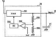
图6是表示在供给字驱动器的驱动电源的给电线(在本说明书中称作“字线驱动电源线”)上,供给升压电位Vword(字线电源电位)构成的一个典型例子的图。参照图6,字线驱动电源线22作为图中未示出的多个字驱动器的电源被连接,将由升压电路20升压外部电源电压Vcc(例如1.8V)后的升压电位(例如6V)供给字线驱动电源线22。在该字线驱动电源线22上连接稳定电容21。6 is a diagram showing a typical example of a configuration for supplying a boosted potential Vword (word line power supply potential) to a power supply line (referred to as "word line drive power line" in this specification) for supplying drive power to a word driver. Referring to FIG. 6, the word line driving
图7是例示图6的升压电路20的典型构成的模式图。参照图7,升压电路20,将例如由分压阻抗2021、2022分压升压电路20的输出电压后的电压,在比较电路203中与基准电压Vref进行电压比较,当升压电路20的输出电压减小,变为基准电压Vref以下时,根据来自比较电路203的比较结果的输出信号,控制环形振荡器(ring oscillator)等的振荡器(OSC)204,使开始振荡,将振荡时钟供给充电泵201,充电泵201在电容(未图示)中蓄积电荷进行升压动作,蓄积到输出平滑电容(未图示)。FIG. 7 is a schematic diagram illustrating a typical configuration of the
可是,在等待(standby)控制的EEPROM中,在等待状态(待机状态)时不进行读访问,字驱动器不被活性化。即等待状态时字线不被选择,字驱动器不驱动字线。因此,等待状态时,升压电路20的升压动作停止(其中,字线驱动电源线例如保持6V电位)。However, in the standby (standby) controlled EEPROM, read access is not performed in the standby state (standby state), and the word driver is not activated. That is, the word line is not selected in the waiting state, and the word driver does not drive the word line. Therefore, in the waiting state, the boosting operation of the
移动电话机、数码相机、附带照相机的移动电话机、PDA(PersonalDigital Assistant)等的电子机器上,搭载作为非易失性存储器的EEPROM。在电池驱动型便携机器上,为谋求低消耗电能化,也要求等待状态时升压电路的低消耗电能化。Electronic devices such as mobile phones, digital cameras, mobile phones with cameras, and PDA (Personal Digital Assistant) are equipped with EEPROM as a non-volatile memory. In battery-driven portable devices, in order to achieve low power consumption, low power consumption of the booster circuit in the standby state is also required.
例如,在图7的升压电路20中,如果将阻抗2021、2022的串联合成阻抗作为R,流过分压阻抗2021、2022的电流作为I,那么由于I=V/R,功率(电能)为VI=V2/R,因此阻抗2021、2022的阻抗值为高阻抗,则功率会降低。然而,当阻抗2021、2022的阻抗值为高阻抗时,比较电路203输入的CR时间常数会增大,输入比较电路203反向输入端子(-)的信号波形的响应会延迟。另外,在图7中,振荡器204,当比较电路203的输入信号在基准电压Vref以下时进行振荡动作,但是当比较电路203的响应延迟时,振荡器204的振荡动作也会延迟,从等待状态向读动作切换时,不能充分对应被活性化的字驱动器的动作带来的字线驱动电源电位的下降,也可能会招致选择单元数据的读出不良。For example, in the
从等待状态向读动作转换时,在维持字线驱动电源电位(也称作“读时升压电位”)时,也可具有图7的使比较电路203的反应速度高速化的构成。此时,可即时实行从等待状态向读动作转换时丢失电荷的供给,但当图7的阻抗2021、2022的阻抗值为低阻抗时,会增大等待时的消耗电流。When switching from the standby state to the read operation, while maintaining the word line driving power supply potential (also referred to as "read-time boost potential"), the configuration of increasing the response speed of the
还有,作为公开下述的与本发明相关的技术的发行物,也可参照已公开的具备两个升压电路构成的下述专利文献1的记载。在该专利文献1中公开了下述的构成:即使电源电压下降,作为稳定地供给在字线电位中采用的升压电压的半导体集成电路(字线升压方式的DRAM),具备第1、第2升压电路,第2升压电路生成比作为第1升压电路生成的字线电位的升压电压Vpp更高的第2升压电压Vpp+α,具备在静电电容元件中蓄积电荷,将升压电压与阈值相比较的比较电路,当由于电源电压Vcc的下降,Vpp降到比该阈值低时,比较电路将控制信号输出到开关部,存储在静电电容单元中的电荷作为电压Vpp供给的构成。但在该专利文献1中记载的构成,只在高电压Vpp下降到比该阈值低时,才会转换到生成Vpp+αα的第2升压电路侧。还有,在闪存存储器的情况下,升压电压即EEPROM的门电压为Vpp+α,这是加速读出模式中的读出干扰(诱发软写入)的主要原因。In addition, as a publication disclosing the technology related to the present invention described below, the description of the following Patent Document 1 which has already disclosed the configuration of two booster circuits can also be referred to. This Patent Document 1 discloses a configuration as a semiconductor integrated circuit (DRAM of a word line boosting method) that stably supplies a boosted voltage used in a word line potential even if the power supply voltage drops, including first, The second booster circuit generates a second boosted voltage Vpp+α that is higher than the boosted voltage Vpp that is a word line potential generated by the first booster circuit, and stores charges in the capacitance element, A comparison circuit that compares the boosted voltage with a threshold value. When Vpp falls below the threshold value due to a drop in the power supply voltage Vcc, the comparison circuit outputs a control signal to the switch section, and the charge stored in the electrostatic capacitance unit is used as the voltage Vpp composition of supply. However, in the configuration described in this Patent Document 1, only when the high voltage Vpp falls below the threshold value, it switches to the side of the second booster circuit that generates Vpp+αα. In addition, in the case of a flash memory, the boosted voltage, that is, the gate voltage of the EEPROM is Vpp+α, which is the main cause of read disturbance (soft write induction) in the accelerated read mode.
如上所述,在图7所示的构成中,阻抗2021、2022的阻抗值为低阻抗时会增加等待时的消耗电流。另一方面,阻抗2021、2022的阻抗值为高阻抗时,减少了等待时的消耗电流,但从等待状态向读动作转换时的响应会延迟,因此,存在字线驱动电源线电位下降或偏差加大的问题。As described above, in the configuration shown in FIG. 7 , when the impedance values of the impedances 2021 and 2022 are low, the current consumption during standby increases. On the other hand, when the impedance values of the impedances 2021 and 2022 are high impedance, the current consumption during standby is reduced, but the response when transitioning from the standby state to the read operation is delayed, so there is a drop in the potential of the word line driving power supply line. Or the problem of increased deviation.
在此,作为折中方案,也可考虑利用下述的构成:例如如图8所示,在字线驱动电源线22与阻抗2021之间具备开关205,其在控制等待状态和读动作切换的等待/读切换信号表示等待状态时导通、表示读动作时截止;在字线驱动电源线22与阻抗2071之间具备开关206,其由反相器208反相等待/读切换信号,由该信号控制导通、截止,在等待/读切换信号表示读动作时导通、表示等待状态时截止;阻抗2021、2022为高阻抗,阻抗2071、2072为低阻抗。等待状态时,作为供给比较电路203分压电压的阻抗,阻抗2021、2022组根据导通状态的开关205被选择;读动作时,低阻抗的2071、2072组根据导通状态的开关206被选择。而且,等待状态时由阻抗2021、2022得到的分压电压和读动作时由阻抗2071、2072得到的分压电压通过开关209选择,供给比较电路203。Here, as a compromise solution, the following configuration can also be considered: for example, as shown inFIG . The waiting/reading switching signal indicates that it is turned on when it is in a waiting state, and it is turned off when it indicates a read action; a switch 206 is provided between the word line drive
然而,如图8所示的构成,分为等待时升压电压维持动作和读时升压电压的维持动作两种模式构成的情况下,从等待状态向读动作切换时,具有控制偏差大的问题。However, when the configuration shown in FIG. 8 is divided into two modes, the operation for maintaining the boosted voltage during standby and the operation for maintaining the boosted voltage during reading, there is a large control deviation when switching from the standby state to the reading operation. question.
图9是用于说明该问题的图,是基于本申请发明者研究、讨论的结果。图9也可作为与本发明的实施例相比较的比较例使用。FIG. 9 is a diagram for explaining this problem, which is based on the research and discussion results of the inventors of the present application. FIG. 9 can also be used as a comparative example for comparison with the examples of the present invention.
等待状态时,EEPROM外部输入的片选通信号CEB被活性化(低电平有效),转换为读动作时,升压电路20(参照图6)的响应延迟,通过读动作时选择字线连接的字驱动器的字线驱动动作,从稳定电容21(参照图6),电荷顺次丢失,弥补这一丢失的升压动作在时间上会产生偏差,其结果使读时的字线驱动电源线22的电位Vword的变化加大。In the waiting state, the chip select signal CEB input from the outside of the EEPROM is activated (active at low level). The word line driving action of the word driver, from the stabilizing capacitor 21 (refer to FIG. 6), the charge is lost sequentially, and the boosting action to make up for this loss will have a deviation in time. As a result, the word line driving power line during reading The change of the potential Vword of 22 increases.
在图9所示的例子中,从ta的等待状态向读动作切换的时间点到tb时间点,升压电路20的升压动作并不充分,每个读动作,字线驱动电源线22的电位Vword的峰值顺次下降。上述升压电位的变动,由于等待状态向读动作切换,例如图8比较电路203的阻抗由高阻抗的2021、2022向低阻抗2071、2072侧切换,CR时间常数即使减小,由于振荡器204振荡时间的变动等,当升压电路20动作延迟时,升压电路20的输出电位的变动变地更大。In the example shown in FIG. 9 , the boosting operation of the
还有,图9的时间点tb以后,升压电路20动作,字线驱动电源电位Vword的峰值电位开始顺次上升。还有,在图9中为彻底说明,按照片选通信号CEB被活性化后,读动作5个周期(X地址变化5次)后,升压动作开始发挥作用的方式进行绘制。Note that, after time tb in FIG. 9 , the
如图9所示,从等待状态向读动作切换时,读时升压电压的下降大是造成数据读出时出错等的原因。As shown in FIG. 9, when switching from the standby state to the read operation, a large drop in the boosted voltage during reading is the cause of errors in data reading.
专利文献1:特开2000-268562号公报(第3页、第1图)Patent Document 1: Japanese Unexamined Patent Application Publication No. 2000-268562 (page 3, drawing 1)
发明内容Contents of the invention
因此,本发明的目的在于提供一种谋求等待时消耗电流减低,并且抑制或减低读时升压电压的变动的电源电路及具备该电源电路的半导体存储装置。Accordingly, an object of the present invention is to provide a power supply circuit that reduces current consumption during standby and suppresses or reduces fluctuations in boosted voltage during reading, and a semiconductor memory device including the power supply circuit.
在本申请中公开的发明为达到上述目的,具有如下概略构成。The invention disclosed in this application has the following schematic configurations in order to achieve the above objects.
与本发明一个方面(侧面)相关的电源电路,具备:输出第1电位的升压电路;蓄积上述升压电路的输出电位的电容;输出与上述第1电位不同的第2电位的电路;根据等待控制信号,在等待状态时处于导通状态,输出上述第2电位到输出端子,在动作时处于截止状态的开关;根据等待控制信号,在等待状态时处于非活性状态,在动作时处于活性状态,接受从上述升压电路输出的上述第1电位作为驱动电源电位,用上述第2电位驱动输出上述输出端子的放大电路。A power supply circuit related to one aspect (side) of the present invention includes: a booster circuit that outputs a first potential; a capacitor that accumulates the output potential of the booster circuit; a circuit that outputs a second potential different from the first potential; Waiting for the control signal, it is in the conducting state in the waiting state, outputs the above-mentioned second potential to the output terminal, and is in the off state when operating; according to the waiting control signal, it is in the inactive state in the waiting state, and is active when operating state, receiving the above-mentioned first potential output from the above-mentioned booster circuit as a driving power supply potential, and driving the amplifier circuit outputting the above-mentioned output terminal with the above-mentioned second potential.
在本发明中,上述第2电位比上述第1电位低,输出上述第2电位的电路是将从上述升压电路输出的上述第1电位分压,输出上述第2电位,或是将其他电路设计为输出上述第2电位的电路,生成升压的上述第2电位。In the present invention, the second potential is lower than the first potential, and the circuit for outputting the second potential divides the first potential output from the booster circuit to output the second potential, or other circuits A circuit designed to output the above-mentioned second potential generates the boosted above-mentioned second potential.
与本发明另一个方面(侧面)相关的电源电路,具备:输出第1电位的升压电路;分压从上述升压电路输出的上述第1电位,生成第2电位的分压电路;连接稳定电容的同时,连接给电对象一个或多个负载电路的给电线;蓄积上述升压电路的输出电位的辅助电容;连接在上述升压电路的输出与上述给电线之间,在等待控制信号表示等待状态时导通,在上述等待控制信号表示动作状态时截止的开关;和接受上述第2电位作为输入电位、输出连接在上述给电线,接受上述升压电路的上述第1电位为驱动电源电位,在上述等待控制信号表示等待状态时处于非活性状态,在上述等待控制信号表示动作状态时被活性化,用上述第2电位驱动上述给电线的放大电路。上述等待状态向动作状态切换时丢失的电荷由上述辅助电容供给。A power supply circuit related to another aspect (side) of the present invention includes: a booster circuit that outputs a first potential; a voltage divider circuit that divides the first potential output from the booster circuit to generate a second potential; the connection is stable At the same time as the capacitor, connect the power supply line of one or more load circuits of the power supply object; the auxiliary capacitor that accumulates the output potential of the above boost circuit; connect between the output of the above boost circuit and the above power supply line, and wait for the control signal to indicate A switch that is turned on in the waiting state and turned off when the above-mentioned waiting control signal indicates an action state; and accepts the above-mentioned second potential as an input potential, the output is connected to the above-mentioned power supply line, and accepts the above-mentioned first potential of the boost circuit as a driving power supply potential , in an inactive state when the standby control signal indicates a standby state, and is activated when the standby control signal indicates an active state, and drives the amplifying circuit of the power supply line with the second potential. Charges lost when the standby state is switched to the operating state are supplied by the storage capacitor.
与本发明的其他方面(侧面)相关的电源电路,具备:输出第1电位的第1升压电路;蓄积上述第1升压电路的输出电位的辅助电容;输出比上述第1电位低的第2电位的第2升压电路;连接稳定电容的同时,连接给电对象一个或多个负载电路的给电线;连接在上述第2升压电路的输出与上述给电线之间,在等待控制信号表示等待状态时导通,在上述等待控制信号表示动作状态时截止的开关;接受来自上述第2升压电路的上述第2电位作为输入电位、输出连接在上述给电线上,接受上述升压电路的上述第1电位为驱动电源电位,在上述等待控制信号表示等待状态时处于非活性状态,在上述等待控制信号表示动作状态时被活性化,用上述第2电位驱动上述给电线的放大电路。上述等待状态向动作状态切换时丢失的电荷由上述辅助电容供给。A power supply circuit related to another aspect (side surface) of the present invention includes: a first booster circuit that outputs a first potential; an auxiliary capacitor that accumulates an output potential of the first booster circuit; and a first booster circuit that outputs a lower potential than the first potential. The second booster circuit with 2 potentials; while connecting the stabilizing capacitor, it is connected to the power supply line of one or more load circuits of the power supply object; it is connected between the output of the above-mentioned second booster circuit and the above-mentioned power supply line, waiting for the control signal A switch that is turned on when it is in a waiting state, and is turned off when the waiting control signal shows an operating state; accepts the second potential from the second booster circuit as an input potential, and connects the output to the power supply line, and receives the second potential from the booster circuit The above-mentioned first potential is a drive power supply potential, which is inactive when the standby control signal indicates a standby state, and is activated when the standby control signal indicates an active state, and drives the amplifying circuit of the power supply line with the second potential. Charges lost when the standby state is switched to the operating state are supplied by the storage capacitor.
与本发明的另一个方面(侧面)相关的半导体存储装置,具备:接受从装置外部供给的电源电位,升压上述电源电位,输出第1电位的升压电路;蓄积上述升压电路输出电位的电容;输出与上述第1电位不同的第2电位的电路;根据输入的等待/访问切换信号,在等待状态时处于导通状态,输出上述第2电位给驱动字线电路的电源线(称“字线驱动电源线”),在访问动作时处于截止状态的开关;根据等待/访问切换信号,在等待状态时处于非活性状态,在访问动作时处于活性状态,接受从上述升压电路输出的上述第1电位作为驱动电源电位,用上述第2电位驱动输出上述字线驱动电源线的放大电路。在本发明中上述第2电位比上述第1电位低,输出上述第2电位的电路构成,可以是分压从上述升压电路输出的上述第1电位,输出上述第2电位或者从其他升压电路生成上述第2电位的构成。A semiconductor memory device according to another aspect (side) of the present invention includes: a booster circuit that receives a power supply potential supplied from outside the device, boosts the power supply potential, and outputs a first potential; and stores an output potential of the booster circuit. Capacitance; a circuit that outputs a second potential different from the above-mentioned first potential; according to the input waiting/access switching signal, it is in a conducting state during the waiting state, and outputs the above-mentioned second potential to the power line of the drive word line circuit (called " Word line drive power line"), a switch that is in the cut-off state during the access action; according to the wait/access switching signal, it is in the inactive state during the wait state, and is in the active state during the access action, and accepts the output from the above boost circuit The first potential is used as a driving power supply potential, and an amplifier circuit that outputs the word line driving power supply line is driven with the second potential. In the present invention, the second potential is lower than the first potential, and the circuit configuration for outputting the second potential can be divided into the first potential output from the booster circuit, outputting the second potential or boosting the second potential from other sources. The circuit generates the above-mentioned second electric potential.
与本发明的其他方面(侧面)相关的半导体存储装置,具备:接受从半导体存储装置外部供给的电源电位,升压上述电源电位,输出第1电位的升压电路;分压从上述升压电路输出的上述第1电位,生成第2电位的分压电路;连接稳定电容的同时,在驱动字线电路上给电驱动电源的字线驱动电源线;蓄积上述升压电路输出电位的辅助电容;连接在上述分压电路的输出与上述字线驱动电源线之间,在输入的等待/访问切换信号表示等待状态时导通,在上述等待/访问切换信号表示访问动作时截止的开关;和接受上述第2电位作为输入电位,输出连接在上述字线驱动电源线上,接受上述升压电路的上述第1电位作为驱动电源电位,在上述等待/访问切换信号表示等待状态时处于非活性状态,在上述等待/访问切换信号表示访问动作时被活性化,用上述第2电位驱动上述字线驱动电源线的放大电路。A semiconductor storage device related to another aspect (side) of the present invention includes: a boost circuit that receives a power supply potential supplied from outside the semiconductor storage device, boosts the power supply potential, and outputs a first potential; divides the voltage from the boost circuit A voltage divider circuit that generates the second potential from the above-mentioned first potential that is output; while connecting a stable capacitor, drive the power line to the word line of the electric drive power supply on the drive word line circuit; an auxiliary capacitor that accumulates the output potential of the above-mentioned booster circuit; A switch that is connected between the output of the above-mentioned voltage divider circuit and the above-mentioned word line drive power line, is turned on when the input waiting/access switching signal indicates a waiting state, and is turned off when the above-mentioned waiting/access switching signal indicates an access action; and accepts The second potential is used as an input potential, the output is connected to the word line driving power supply line, the first potential of the boost circuit is received as a driving power supply potential, and it is in an inactive state when the waiting/access switching signal indicates a waiting state, The amplifying circuit that is activated when the standby/access switching signal indicates an access operation and drives the word line driving power supply line with the second potential.
与本发明的其他方面(侧面)相关的半导体存储装置,具备:接受从半导体存储装置外部供给的电源电位,升压上述电源电位,输出第1电位的第1升压电路;输出比上述第1电位低的第2电位的第2升压电路;蓄积上述第1升压电路的输出电位的辅助电容;连接稳定电容的同时,在驱动字线的电路上给电驱动电源的字线驱动电源线;连接在上述第2升压电路的输出与上述字线驱动电源线之间,在输入的等待/访问切换信号表示等待状态时导通,在上述等待/访问切换信号表示访问动作时截止的开关;接受来自上述第2升压电路的上述第2电位作为输入,输出连接在上述字线驱动电源线上,接受上述升压电路的上述第1电位作为驱动电源电位,上述等待/访问切换信号表示等待状态时处于非活性化状态,上述等待/访问切换信号表示访问动作时被活性化,用上述第2电位驱动上述字线驱动电源线的放大电路。A semiconductor storage device related to another aspect (side) of the present invention includes: a first booster circuit that receives a power supply potential supplied from outside the semiconductor storage device, boosts the power supply potential, and outputs a first potential; The second booster circuit of the second potential with a low potential; the auxiliary capacitor for accumulating the output potential of the first booster circuit; and the word line drive power line for the electric drive power supply to the circuit for driving the word line while connecting the stabilizing capacitor ; A switch connected between the output of the above-mentioned second booster circuit and the above-mentioned word line driving power supply line, turned on when the input standby/access switching signal indicates a waiting state, and turned off when the above-mentioned waiting/access switching signal indicates an access operation ;Accept the above-mentioned second potential from the above-mentioned second booster circuit as an input, the output is connected to the above-mentioned word line drive power supply line, accept the above-mentioned first potential of the above-mentioned booster circuit as a drive power supply potential, and the above-mentioned waiting/access switching signal indicates It is in an inactive state in the standby state, and the standby/access switching signal indicates that it is activated in an access operation, and drives the amplifier circuit of the word line driving power supply line with the second potential.
(发明效果)(invention effect)
根据本发明,即谋求了等待时升压电路的消耗电能的减低,又能抑制从等待向动作切换时供给给电线的升压电位的变动。According to the present invention, while reducing the power consumption of the booster circuit during standby, it is possible to suppress fluctuations in the boosted potential supplied to the wire when switching from standby to operation.
附图说明Description of drawings
图1是表示本发明第1实施方式的构成图。FIG. 1 is a configuration diagram showing a first embodiment of the present invention.
图2是用于说明本发明第1实施方式的动作的一例的时序波形图。FIG. 2 is a timing waveform diagram illustrating an example of the operation of the first embodiment of the present invention.
图3是表示本发明第2实施方式的构成图。Fig. 3 is a configuration diagram showing a second embodiment of the present invention.
图4是用于说明本发明第2实施方式的动作的一例的时序波形图。FIG. 4 is a timing waveform diagram illustrating an example of the operation of the second embodiment of the present invention.
图5是表示本发明中放大电路和开关构成的一实施示例图。Fig. 5 is a diagram showing an embodiment example of an amplifier circuit and a switch configuration in the present invention.
图6是表示以往的供给字线电源的电源电路的构成图。FIG. 6 is a configuration diagram showing a conventional power supply circuit for supplying power to word lines.
图7是用于说明升压电路的图。FIG. 7 is a diagram for explaining a booster circuit.
图8是用于说明阻抗切换型升压电路的图。FIG. 8 is a diagram for explaining an impedance switching type booster circuit.
图9是说明图6动作的波形图。Fig. 9 is a waveform diagram illustrating the operation of Fig. 6 .
图中:20-升压电路;21-稳定电容;22-字线驱动电源线;101-升压电路;102-辅助电容;103-稳定电容;104-放大电路;105-开关;106-节点(Vpool电位);1071、1072-阻抗;108-节点(Vread电位);109-字线驱动电源线;110-升压电路;111-电平移位电路;201-充电泵;2021、2022-阻抗;203-比较电路;204-振荡器;205-开关;206-开关;208-反相器;209-开关。In the figure: 20-boosting circuit; 21-stabilizing capacitor; 22-word line driving power line; 101-boosting circuit; 102-auxiliary capacitor; 103-stabilizing capacitor; 104-amplifying circuit; 105-switch; 106-node (Vpool potential); 1071 , 1072 -impedance; 108-node (Vread potential); 109-word line drive power line; 110-boost circuit; 111-level shift circuit; 201-charge pump; 2021 , 2022 —impedance; 203—comparison circuit; 204—oscillator; 205—switch; 206—switch; 208—inverter; 209—switch.
具体实施方式Detailed ways
为进一步详细说明本发明,下面参照附图,对用于实施发明的最佳方式进行说明。图1是表示本发明的第1实施方式的构成的图。In order to further explain the present invention in detail, the best mode for carrying out the invention will be described below with reference to the accompanying drawings. FIG. 1 is a diagram showing the configuration of a first embodiment of the present invention.
参照图1,与本发明的第1实施方式相关的半导体存储装置是用比外部电源电位Vcc(例如1.8V)更高的电压驱动字线的半导体存储装置,具备输入外部电源电压Vcc、输出比Vcc高的电位的升压电位Vpool(例如7V)的升压电路101;一端与升压电路101的输出节点106连接,另一端例如与地电位连接的辅助电容102;连接在升压电路101的输出节点106与地之间,从抽头处输出分压升压电路101的升压电压Vpool后的电压(例如6V)的分压阻抗1071、1072;输入端子连接在分压阻抗1071、1072的连接点(抽头),接受升压电位Vpool作为驱动电源电位,根据等待/读切换信号,控制活性化/非活性化的放大电路(AMP)104;一端连接分压阻抗1071、1072的连接点,另一端连接字线驱动电源线109,根据等待/读切换信号控制导通、截止的开关105。字线驱动电源线109一端连接在放大电路104的输出端子上,另一端连接在一端接地的稳定电容103的另一端上。字线驱动电源线109连接在图中未示出的字驱动器(驱动接受X译码器的输出的驱动字线)的电源基座(pad)上。Referring to FIG. 1, the semiconductor storage device related to the first embodiment of the present invention is a semiconductor storage device that drives a word line at a voltage higher than the external power supply potential Vcc (for example, 1.8V), and has an input external power supply voltage Vcc, an output ratio A booster circuit 101 of a booster potential Vpool (such as 7V) with a high potential of Vcc; one end is connected to the output node 106 of the booster circuit 101, and the other end is connected to an auxiliary capacitor 102 connected to the ground potential; connected to the booster circuit 101 Between the output node 106 and the ground, the taps output voltage division impedances 1071 , 1072 of the boosted voltage Vpool of the voltage division booster circuit 101 (for example, 6V); the input terminals are connected to the voltage division impedance 1071 , The connection point (tap) of 1072 accepts the boosted potential Vpool as the driving power supply potential, and controls the active/inactive amplifying circuit (AMP) 104 according to the waiting/reading switching signal; one end is connected to the voltage dividing impedance 1071 , 1072 , the other end is connected to the word line drive power line 109, and the switch 105 is controlled to be turned on or off according to the wait/read switching signal. One end of the word line
放大电路104根据等待/读切换信号,在等待时处于非活性化状态(停止动作),放大电路104的输出处于高阻抗状态,在读动作时被切换控制为活性状态。The amplifying
开关105根据等待/读切换信号,在等待时处于导通状态,读动作时处于截止状态。等待/读切换信号是根据从半导体存储装置外部输入到控制端子(CEB)的片选通信号CEB,在半导体存储装置内部生成的控制信号。The
图2是用于说明图1所示的本实施例动作的时序波形图。图2中模式表示了从半导体存储装置外部输入到控制端子(CEB)的片选通信号CEB、X地址、Vpool(节点106的电位)、Vread(节点108的电位)、Vword(节点109的电位)的波形变化例子。参照图1及图2,以下说明第1实施方式的动作。Fig. 2 is a timing waveform diagram for explaining the operation of the present embodiment shown in Fig. 1 . 2 schematically shows the chip select signal CEB, X address, Vpool (potential of node 106), Vread (potential of node 108), Vword (potential of node 109) input from the outside of the semiconductor storage device to the control terminal (CEB). ) waveform change example. The operation of the first embodiment will be described below with reference to FIGS. 1 and 2 .
片选通信号CEB为非活性状态(高电平)时,等待/读切换信号处于等待状态,放大电路104处于非活性化状态,其输出为高阻抗状态。另一方面,开关105处于导通状态。因此,等待状态时升压电路101的升压电压Vpool由阻抗1071、1072分压后的电压Vread(例如6V)介由导通状态的开关105,供给字线驱动电源线109。字线驱动电源线109的电位为Vread。When the chip select signal CEB is in an inactive state (high level), the wait/read switching signal is in a wait state, the amplifying
片选通信号CEB为活性状态(低电平)时,读动作时开关105处于截止状态,放大电路104处于活性状态。放大电路104接受由阻抗1071、1072分压升压电压Vpool后的电压Vread,用电压Vread驱动字线驱动电源线109。When the chip select signal CEB is in the active state (low level), the
优选放大电路104的构成为电压跟随器(Voltage follower),字线驱动电源线109的电压Vword与放大电路104的输入电压Vread同相。升压电压Vpool由阻抗1071、1072分压后的电压Vread(图1的节点108的电位),读动作时与升压电压Vpool同相,故由放大电路104驱动的字线驱动电源线109的电压Vword也与Vpool同相。Preferably, the amplifying
在本实施例中,从等待状态向读动作转换时,读动作时的电荷从在等待时进行蓄积的辅助电容102供给。因此,在从等待状态向读动作切换时,与图9所示的以往的构成的情况相比,字线驱动电源线109的电位Vword的变化,可被抑制、减低。In the present embodiment, when transitioning from the standby state to the read operation, charges during the read operation are supplied from the
即从升压电路101输出的升压电位Vpool的峰值,在从等待状态向读动作切换时,虽然随着每次电荷丢失顺次下降,但由于供给来自辅助电容102的电荷,与图9的示例相比,字线驱动电源线109的电位下降的变动幅度变小。That is, the peak value of the boosted potential Vpool output from the
还有,在图1中生成电位Vread的阻抗1071、1072由高阻抗构成,因此当然也可以在等待状态和读动作时都作为谋求减低消耗电能的构成。In addition, since the impedances 1071 and 1072 generating the potential Vread in FIG. 1 are made of high impedance, it is of course possible to reduce the power consumption in both the standby state and the read operation.
接着,说明本发明第2实施方式的构成。图3是表示本发明第2实施方式的构成图。参照图3,有关本发明的第2实施方式的半导体存储装置,具备:输入外部电源电压Vcc(例如1.8V)、输出比Vcc高的电位的升压电位Vpool(例如7V)的升压电路101;一端与升压电路101的输出节点106连接、另一端接地的辅助电容102;输出比Vcc高的电位的升压电位Vread(例如6V)的升压电路110。但Vread比Vpool电位低。Next, the configuration of the second embodiment of the present invention will be described. Fig. 3 is a configuration diagram showing a second embodiment of the present invention. Referring to FIG. 3 , the semiconductor storage device according to the second embodiment of the present invention includes: a
升压电路110的输出电位Vread输入到放大电路104的输入端子,并且还输入到根据等待/读切换信号,控制导通、截止的开关105的一端。开关105的另一端连接字线驱动电源线109,放大电路104的输出端子连接字线驱动电源线109。与上述第1实施方式相同,本实施方式中也在字线驱动电源线109上连接稳定电容103。The output potential Vread of the
与上述第1实施方式相同,在第2实施方式中,放大电路104也根据等待/读切换信号,在等待时处于非活性状态,输出端子处于高阻抗状态,在读动作时处于活性状态。Similar to the above-mentioned first embodiment, in the second embodiment, the amplifying
另外,开关105根据等待/读切换信号,在等待时处于导通状态,在读动作时处于截止状态。等待/读切换信号是根据从半导体存储装置外部输入到控制端子(插头(pin))的片选通信号CEB,在半导体存储装置内部生成的控制信号。In addition, the
图4是用于说明在图3中所示的本实施方式的动作的时序波形图。在图4中模式地表示了从半导体存储装置外部输入到控制端子(CEB)的片选通信号CEB、X地址、Vpool(节点106的电位)、Vread(节点108的电位)、Vword(字线驱动电源线109的电位)的波形变化的例子。参照图3及图4,以下说明第2实施方式的动作。FIG. 4 is a timing waveform diagram for explaining the operation of the present embodiment shown in FIG. 3 . 4 schematically shows the chip select signal CEB, X address, Vpool (the potential of node 106), Vread (the potential of node 108), Vword (the potential of the word line) input from outside the semiconductor storage device to the control terminal (CEB). An example of a waveform change of the potential of the driving power supply line 109). The operation of the second embodiment will be described below with reference to FIGS. 3 and 4 .
片选通信号CEB为非活性状态(高电平)时,等待/读切换信号处于等待状态,放大电路104处于非活性化状态,其输出为高阻抗状态,开关105处于导通状态。因此,等待状态时,在字线驱动电源线109上介由开关105供给来自升压电路110的电压Vread。When the chip select signal CEB is in the inactive state (high level), the wait/read switching signal is in the wait state, the amplifying
片选通信号CEB变为活性状态(低电平),等待/读切换信号表示读动作时,开关105处于截止状态,放大电路104处于活性状态,在输入端子接受升压电路110的输出电位Vread,由电位Vread驱动字线驱动电源线109。Chip strobe signal CEB becomes active (low level), and when the wait/read switching signal indicates a read action,
与上述第1实施方式不同,第2实施方式在读动作时,升压电路110的输出电位Vread(节点108的电位)保持恒定。这是因为升压电路110的输出连接在输入阻抗高的放大电路104上,读动作时开关105被截止,输出电位Vread(节点108)的电荷不会丢失。Unlike the above-mentioned first embodiment, in the second embodiment, the output potential Vread (the potential of the node 108 ) of the
放大电路104具有变为由与输入电压相同的电压驱动输出端子的电压跟随器构成。读动作时的电荷,由在等待时蓄积电荷的辅助电容102供给,所以从等待状态向读动作转换时,与图9所示的比较例相比,字线驱动电源线109的电位Vword的变化,可被特别地减小。The amplifying
另外,放大电路104用电压Vread驱动字线驱动电源线109。因此,虽然从升压电路101输出的升压电压Vpool的峰值,根据读动作每次电荷丢失而顺次下降,但字线驱动电源线109的电位的峰值在每个读周期,恢复为6V(Vread)。即峰值维持在6V。因此,在选择单元的字线上供给6V的字线电源,使读动作稳定化。In addition, the amplifying
图5是表示在图1及图3所示的实施例中的放大电路104和开关105的构成的一个实施例图。FIG. 5 is a diagram showing an example of the configuration of the
参照图5,放大电路104由差动放大电路构成,具备:构成供给差动对恒电流的恒流源NMOS晶体管MN3;源极与NMOS晶体管MN3的漏极共同连接构成差动对的NMOS晶体管MN1、MN2;构成差动对能动负载的电流镜电路(PMOS晶体管MP1、MP2)。构成电流镜的PMOS晶体管MP1、MP2的源极与电位Vpool(图1或图3的节点106)连接。构成恒流源的NMOS晶体管MN3,连接到源极接地、栅极输入等待/读切换信号的NMOS晶体管MN4的漏极。Referring to Fig. 5, the amplifying
差动对的输出(晶体管MN1和MP1的漏极连接点),连接到源极连接Vpool(节点106)、漏极连接字线驱动电源线109、构成输出放大段的PMOS晶体管MP4的栅极。The output of the differential pair (the drain connection point of transistors MN1 and MP1 ) is connected to the source connection Vpool (node 106 ), the drain connection to the word line drive
PMOS晶体管MP4的漏极与字线驱动电源线109之间的连接点,介由阻抗R连接NMOS晶体管MN5的漏极,NMOS晶体管MN5的源极接地,其栅极连接等待/读切换信号。The connection point between the drain of the PMOS transistor MP4 and the word line driving
另外,等待/读切换信号输入到电平移位(level shift)电路111中进行电平移位,还具备栅极上输入经电平移位的等待/读切换信号、源极连接电源Vpool(节点106)、漏极连接输出放大段PMOS晶体管MP4的栅极的PMOS晶体管MP3。In addition, the waiting/reading switching signal is input to the level shift (level shift)
还有,具备源极连接Vread(图1或图3的节点108)、栅极上输入电平移位的等待/读切换信号的PMOS晶体管MP5,和源极连接字线驱动电源线109、栅极上输入经电平移位的等待/读切换信号、漏极与PMOS晶体管MP5的漏极连接的PMOS晶体管MP6。In addition, the source is connected to Vread (the
在差动对NMOS晶体管MN1的栅极(非反相输入端子)上接受电位Vread,在差动对NMOS晶体管MN2的栅极(反相输入端子)上连接差动放大电路输出端子(图5中字线驱动电源线109),构成电压跟随放大器。Receive the potential Vread on the gate (non-inverting input terminal) of the differential pair NMOS transistor MN1, and connect the output terminal of the differential amplifier circuit on the gate (inverting input terminal) of the differential pair NMOS transistor MN2 (the word in FIG. 5 Line drives the power line 109) to form a voltage follower amplifier.
另外,PMOS晶体管MP3、MP5、MP6构成图1、图3的开关105。In addition, the PMOS transistors MP3, MP5, and MP6 constitute the
电平移位电路111将用于控制PMOS晶体管MP3、MP5、MP6导通、截止的等待/读切换信号移位成与升压电压Vpool、Vread对应的振幅信号。当PMOS晶体管MP3、MP5、MP6截止时,PMOS晶体管MP3、MP5、MP6的栅极输入的等待/读切换信号的电位为Vread,另一方面,当PMOS晶体管MP3、MP5、MP6导通时,PMOS晶体管MP3、MP5、MP6的栅极输入的等待/读切换信号的电位为地电位。还有,级联(共射共基(cascode)连接)在Vread与字线驱动电源线109之间的PMOS晶体管MP5、MP6可阻止从字线驱动电源线109向Vread(节点108)的电流逆流。The
以下说明图5所示的差动放大电路的动作。The operation of the differential amplifier circuit shown in FIG. 5 will be described below.
本实施例中,等待状态时,等待/读切换信号处于低电平,恒流源NMOS晶体管MN4及输出放大段的NMOS晶体管MN5都处于截止状态。而且,等待/读切换信号因处于低电平,PMOS晶体管MP3导通、PMOS晶体管MP4的栅极为电位Vpool。这样,输出放大段的PMOS晶体管MP4截止,差动放大电路的输出处于高阻抗状态。另一方面,由于PMOS晶体管MP5、MP6处于导通状态,因此图1或图3中节点108的电位Vread(6V)供给字线驱动电源线109。In this embodiment, in the waiting state, the waiting/reading switch signal is at a low level, and the constant current source NMOS transistor MN4 and the NMOS transistor MN5 of the output amplification section are both in a cut-off state. Furthermore, since the wait/read switching signal is at a low level, the PMOS transistor MP3 is turned on, and the gate of the PMOS transistor MP4 is at the potential Vpool. In this way, the PMOS transistor MP4 of the output amplification section is turned off, and the output of the differential amplifier circuit is in a high impedance state. On the other hand, since the PMOS transistors MP5 and MP6 are turned on, the potential Vread (6V) at the
如上所述,根据本实施例,等待状态时,放大电路104中的电源电流通路被阻断,放大电路104停止动作,谋求了消耗电能的减低。As described above, according to this embodiment, the power supply current path in the
本实施例中,读动作时,等待/读切换信号处于高电平,恒流源NMOS晶体管MN4及输出放大段的NMOS晶体管MN5都处于导通状态,差动放大电路被活性化。另外,PMOS晶体管MP3、MP5、MP6都截止,输出放大段的PMOS晶体管MP4,其栅极接受差动对(MN1、MN2)的输出,充电驱动字线驱动电源线109。还有,等待/读切换信号为高电平时,介由阻抗R连接字线驱动电源线109的NMOS晶体管MN5,放电驱动字线驱动电源线109。差动对(MN1、MN2)的反相输入端子(NMOS晶体管MN2的栅极)的电位比电位Vread低时,暂时流入差动对一方的NMOS晶体管MN2的电流(漏极—源极电流)减少、流入差动对另一方的NMOS晶体管MN1的电流(漏极—源极电流)增加,PMOS晶体管MP3的栅极电位下降,流入PMOS晶体管MP3的电流(漏极—源极电流)增加,使字线驱动电源线109的电位上升。另一方面,差动对(MN1、MN2)的反相输入端子(NMOS晶体管MN2栅极)的电位比电位Vread高时,暂时流入差动对一方的NMOS晶体管MN2的电流(漏极—源极电流)增加、流入差动对另一方的NMOS晶体管MN1的电流(漏极—源极电流)减少,PMOS晶体管MP3的栅极电位上升,流入PMOS晶体管MP3的电流(漏极—源极电流)减少,使字线驱动电源线109的电位下降。这样,图5的差动放大电路,发挥着由与输入非反相输入端子的电位Vread同相的电位驱动字线驱动电源线109的电压跟随电路的功能。还有,PMOS晶体管MP4的漏极与栅极之间,当然也可具备电容元件(防止振荡用的电容元件)。In this embodiment, during the read operation, the wait/read switching signal is at a high level, the constant current source NMOS transistor MN4 and the NMOS transistor MN5 of the output amplification section are both in the conduction state, and the differential amplifier circuit is activated. In addition, the PMOS transistors MP3, MP5, and MP6 are all turned off, and the gate of the PMOS transistor MP4 in the output amplifier section receives the output of the differential pair (MN1, MN2) to charge and drive the word line to drive the
还有,在图1所示的上述实施方式等中,作为升压电路101,当然也可具有如图8所示的根据等待/读切换信号,由开关转换高阻抗与低阻抗的构成。In addition, in the above-mentioned embodiment shown in FIG. 1, as the
以上虽然结合上述实施例说明本发明,但本发明并不仅仅限定为上述实施例的构成,可适用于实现等待状态和活性状态切换的任意电源电路。另外,本发明也不限定只适用于半导体存储装置的升压电路,当然也可适用于任意电子装置。Although the present invention has been described above in conjunction with the above embodiments, the present invention is not limited to the configuration of the above embodiments, and is applicable to any power supply circuit that realizes switching between a standby state and an active state. In addition, the present invention is not limited to a booster circuit applicable only to a semiconductor storage device, and is of course applicable to any electronic device.
Claims (14)
Applications Claiming Priority (2)
| Application Number | Priority Date | Filing Date | Title |
|---|---|---|---|
| JP2004093532AJP4377274B2 (en) | 2004-03-26 | 2004-03-26 | Power supply circuit and semiconductor memory device provided with the power supply circuit |
| JP2004093532 | 2004-03-26 |
Publications (1)
| Publication Number | Publication Date |
|---|---|
| CN1674155Atrue CN1674155A (en) | 2005-09-28 |
Family
ID=34989632
Family Applications (1)
| Application Number | Title | Priority Date | Filing Date |
|---|---|---|---|
| CNA2005100624222APendingCN1674155A (en) | 2004-03-26 | 2005-03-28 | Power supply circuit and semiconductor storage device with the power supply circuit |
Country Status (3)
| Country | Link |
|---|---|
| US (1) | US7042788B2 (en) |
| JP (1) | JP4377274B2 (en) |
| CN (1) | CN1674155A (en) |
Cited By (5)
| Publication number | Priority date | Publication date | Assignee | Title |
|---|---|---|---|---|
| CN101414485B (en)* | 2007-10-19 | 2011-03-16 | 英业达股份有限公司 | power supply |
| CN101656108B (en)* | 2008-08-19 | 2012-06-27 | 杭州士兰微电子股份有限公司 | Power supply circuit and application method |
| CN103377696A (en)* | 2012-04-24 | 2013-10-30 | 北京兆易创新科技股份有限公司 | System for supplying stable voltage to storage unit |
| CN107958684A (en)* | 2016-10-18 | 2018-04-24 | 爱思开海力士有限公司 | Voltage regulator and there is its resistance-change memory device |
| CN110211623A (en)* | 2019-07-04 | 2019-09-06 | 合肥联诺科技有限公司 | A kind of power-supply system of NOR FLASH memory cell array |
Families Citing this family (9)
| Publication number | Priority date | Publication date | Assignee | Title |
|---|---|---|---|---|
| KR20060034025A (en)* | 2004-10-18 | 2006-04-21 | 삼성전자주식회사 | Voltage generating device and method thereof, display device having same and driving device thereof |
| US7515457B2 (en)* | 2006-02-24 | 2009-04-07 | Grandis, Inc. | Current driven memory cells having enhanced current and enhanced current symmetry |
| US7626865B2 (en)* | 2006-06-13 | 2009-12-01 | Micron Technology, Inc. | Charge pump operation in a non-volatile memory device |
| US7599231B2 (en)* | 2006-10-11 | 2009-10-06 | Atmel Corporation | Adaptive regulator for idle state in a charge pump circuit of a memory device |
| KR100863015B1 (en)* | 2007-05-11 | 2008-10-13 | 주식회사 하이닉스반도체 | Voltage stabilization circuit and semiconductor memory device using same |
| JP2010198667A (en)* | 2009-02-24 | 2010-09-09 | Toshiba Corp | Semiconductor storage apparatus |
| US8611172B2 (en)* | 2012-05-21 | 2013-12-17 | Arm Limited | Controlling a voltage level of an access signal to reduce access disturbs in semiconductor memories |
| JP2023021810A (en)* | 2021-08-02 | 2023-02-14 | キオクシア株式会社 | Semiconductor device, memory controller, voltage correction method and voltage correction program |
| US20250006246A1 (en)* | 2023-06-29 | 2025-01-02 | Advanced Micro Devices, Inc. | Rc-tuned wordline underdrive circuit |
Family Cites Families (3)
| Publication number | Priority date | Publication date | Assignee | Title |
|---|---|---|---|---|
| US5262999A (en)* | 1988-06-17 | 1993-11-16 | Hitachi, Ltd. | Large scale integrated circuit for low voltage operation |
| JP2000268562A (en) | 1999-03-15 | 2000-09-29 | Hitachi Ltd | Semiconductor integrated circuit device |
| US6841983B2 (en)* | 2002-11-14 | 2005-01-11 | Fyre Storm, Inc. | Digital signal to pulse converter and method of digital signal to pulse conversion |
- 2004
- 2004-03-26JPJP2004093532Apatent/JP4377274B2/ennot_activeExpired - Fee Related
- 2005
- 2005-03-24USUS11/087,663patent/US7042788B2/ennot_activeExpired - Lifetime
- 2005-03-28CNCNA2005100624222Apatent/CN1674155A/enactivePending
Cited By (8)
| Publication number | Priority date | Publication date | Assignee | Title |
|---|---|---|---|---|
| CN101414485B (en)* | 2007-10-19 | 2011-03-16 | 英业达股份有限公司 | power supply |
| CN101656108B (en)* | 2008-08-19 | 2012-06-27 | 杭州士兰微电子股份有限公司 | Power supply circuit and application method |
| CN103377696A (en)* | 2012-04-24 | 2013-10-30 | 北京兆易创新科技股份有限公司 | System for supplying stable voltage to storage unit |
| CN103377696B (en)* | 2012-04-24 | 2016-06-08 | 北京兆易创新科技股份有限公司 | A kind of system for storage unit offer stabilized voltage |
| CN107958684A (en)* | 2016-10-18 | 2018-04-24 | 爱思开海力士有限公司 | Voltage regulator and there is its resistance-change memory device |
| CN107958684B (en)* | 2016-10-18 | 2021-06-18 | 爱思开海力士有限公司 | Voltage regulator and resistive memory device having the same |
| CN110211623A (en)* | 2019-07-04 | 2019-09-06 | 合肥联诺科技有限公司 | A kind of power-supply system of NOR FLASH memory cell array |
| CN110211623B (en)* | 2019-07-04 | 2021-05-04 | 合肥联诺科技股份有限公司 | Power supply system of NOR FLASH memory cell array |
Also Published As
| Publication number | Publication date |
|---|---|
| JP2005285163A (en) | 2005-10-13 |
| US20050213412A1 (en) | 2005-09-29 |
| US7042788B2 (en) | 2006-05-09 |
| JP4377274B2 (en) | 2009-12-02 |
Similar Documents
| Publication | Publication Date | Title |
|---|---|---|
| US6356499B1 (en) | Power supply circuit and semiconductor memory device having the same | |
| CN1285171C (en) | Oscillation circuit, booster circuit, nonvolatile memory device, and semiconductor device | |
| JP4094104B2 (en) | Semiconductor integrated circuit device and memory device | |
| JP5504507B2 (en) | Integrated circuit device | |
| US7652522B2 (en) | High efficiency low cost bi-directional charge pump circuit for very low voltage applications | |
| CN1674155A (en) | Power supply circuit and semiconductor storage device with the power supply circuit | |
| CN1453762A (en) | Efficient liquid crystal display drive voltage generating circuit and its method | |
| JP3151123B2 (en) | Nonvolatile semiconductor memory device | |
| TW200428743A (en) | High voltage ripple reduction and substrate protection | |
| US7439792B2 (en) | High voltage generation circuit and semiconductor device having the same | |
| CN1538453B (en) | Boost power supply circuit | |
| CN1449566A (en) | Regulator design for inductive booster pump using pulse width modulation technique | |
| JP2012244660A (en) | Semiconductor device with step-up circuit | |
| US10650866B2 (en) | Charge pump drive circuit | |
| JP2010124618A (en) | Power supply circuit | |
| US8519778B2 (en) | Semiconductor integrated circuit and booster circuit including the same | |
| JP2009017717A (en) | Step-up circuit | |
| CN1237767A (en) | Semiconductor memory device | |
| CN1703779A (en) | semiconductor integrated circuit | |
| CN116317542A (en) | A dual charge pump circuit system | |
| CN1921012A (en) | Circuit for generating step-up voltage in non-volatile memory device | |
| US8593874B2 (en) | Voltage generation circuit which is capable of reducing circuit area | |
| JPH1069796A (en) | Semiconductor integrated circuit with high-speed test function | |
| US9952615B2 (en) | Charge pump and voltage generation circuit | |
| JP2007323684A (en) | Semiconductor integrated circuit |
Legal Events
| Date | Code | Title | Description |
|---|---|---|---|
| C06 | Publication | ||
| PB01 | Publication | ||
| C10 | Entry into substantive examination | ||
| SE01 | Entry into force of request for substantive examination | ||
| C02 | Deemed withdrawal of patent application after publication (patent law 2001) | ||
| WD01 | Invention patent application deemed withdrawn after publication |