CN1663038A - laser processing - Google Patents
laser processingDownload PDFInfo
- Publication number
- CN1663038A CN1663038ACN03814249XACN03814249ACN1663038ACN 1663038 ACN1663038 ACN 1663038ACN 03814249X ACN03814249X ACN 03814249XACN 03814249 ACN03814249 ACN 03814249ACN 1663038 ACN1663038 ACN 1663038A
- Authority
- CN
- China
- Prior art keywords
- laser
- substrate
- die
- layer
- cutting
- Prior art date
- Legal status (The legal status is an assumption and is not a legal conclusion. Google has not performed a legal analysis and makes no representation as to the accuracy of the status listed.)
- Pending
Links
Images


Classifications
- B—PERFORMING OPERATIONS; TRANSPORTING
- B23—MACHINE TOOLS; METAL-WORKING NOT OTHERWISE PROVIDED FOR
- B23K—SOLDERING OR UNSOLDERING; WELDING; CLADDING OR PLATING BY SOLDERING OR WELDING; CUTTING BY APPLYING HEAT LOCALLY, e.g. FLAME CUTTING; WORKING BY LASER BEAM
- B23K26/00—Working by laser beam, e.g. welding, cutting or boring
- B23K26/12—Working by laser beam, e.g. welding, cutting or boring in a special atmosphere, e.g. in an enclosure
- B23K26/126—Working by laser beam, e.g. welding, cutting or boring in a special atmosphere, e.g. in an enclosure in an atmosphere of gases chemically reacting with the workpiece
- B—PERFORMING OPERATIONS; TRANSPORTING
- B23—MACHINE TOOLS; METAL-WORKING NOT OTHERWISE PROVIDED FOR
- B23K—SOLDERING OR UNSOLDERING; WELDING; CLADDING OR PLATING BY SOLDERING OR WELDING; CUTTING BY APPLYING HEAT LOCALLY, e.g. FLAME CUTTING; WORKING BY LASER BEAM
- B23K26/00—Working by laser beam, e.g. welding, cutting or boring
- B23K26/02—Positioning or observing the workpiece, e.g. with respect to the point of impact; Aligning, aiming or focusing the laser beam
- B23K26/06—Shaping the laser beam, e.g. by masks or multi-focusing
- B23K26/064—Shaping the laser beam, e.g. by masks or multi-focusing by means of optical elements, e.g. lenses, mirrors or prisms
- B23K26/0648—Shaping the laser beam, e.g. by masks or multi-focusing by means of optical elements, e.g. lenses, mirrors or prisms comprising lenses
- B—PERFORMING OPERATIONS; TRANSPORTING
- B23—MACHINE TOOLS; METAL-WORKING NOT OTHERWISE PROVIDED FOR
- B23K—SOLDERING OR UNSOLDERING; WELDING; CLADDING OR PLATING BY SOLDERING OR WELDING; CUTTING BY APPLYING HEAT LOCALLY, e.g. FLAME CUTTING; WORKING BY LASER BEAM
- B23K26/00—Working by laser beam, e.g. welding, cutting or boring
- B23K26/12—Working by laser beam, e.g. welding, cutting or boring in a special atmosphere, e.g. in an enclosure
- B23K26/123—Working by laser beam, e.g. welding, cutting or boring in a special atmosphere, e.g. in an enclosure in an atmosphere of particular gases
- B—PERFORMING OPERATIONS; TRANSPORTING
- B23—MACHINE TOOLS; METAL-WORKING NOT OTHERWISE PROVIDED FOR
- B23K—SOLDERING OR UNSOLDERING; WELDING; CLADDING OR PLATING BY SOLDERING OR WELDING; CUTTING BY APPLYING HEAT LOCALLY, e.g. FLAME CUTTING; WORKING BY LASER BEAM
- B23K26/00—Working by laser beam, e.g. welding, cutting or boring
- B23K26/36—Removing material
- B23K26/40—Removing material taking account of the properties of the material involved
- H—ELECTRICITY
- H01—ELECTRIC ELEMENTS
- H01L—SEMICONDUCTOR DEVICES NOT COVERED BY CLASS H10
- H01L21/00—Processes or apparatus adapted for the manufacture or treatment of semiconductor or solid state devices or of parts thereof
- H01L21/70—Manufacture or treatment of devices consisting of a plurality of solid state components formed in or on a common substrate or of parts thereof; Manufacture of integrated circuit devices or of parts thereof
- H01L21/77—Manufacture or treatment of devices consisting of a plurality of solid state components or integrated circuits formed in, or on, a common substrate
- H01L21/78—Manufacture or treatment of devices consisting of a plurality of solid state components or integrated circuits formed in, or on, a common substrate with subsequent division of the substrate into plural individual devices
- B—PERFORMING OPERATIONS; TRANSPORTING
- B23—MACHINE TOOLS; METAL-WORKING NOT OTHERWISE PROVIDED FOR
- B23K—SOLDERING OR UNSOLDERING; WELDING; CLADDING OR PLATING BY SOLDERING OR WELDING; CUTTING BY APPLYING HEAT LOCALLY, e.g. FLAME CUTTING; WORKING BY LASER BEAM
- B23K2101/00—Articles made by soldering, welding or cutting
- B23K2101/36—Electric or electronic devices
- B23K2101/40—Semiconductor devices
- B—PERFORMING OPERATIONS; TRANSPORTING
- B23—MACHINE TOOLS; METAL-WORKING NOT OTHERWISE PROVIDED FOR
- B23K—SOLDERING OR UNSOLDERING; WELDING; CLADDING OR PLATING BY SOLDERING OR WELDING; CUTTING BY APPLYING HEAT LOCALLY, e.g. FLAME CUTTING; WORKING BY LASER BEAM
- B23K2103/00—Materials to be soldered, welded or cut
- B23K2103/50—Inorganic material, e.g. metals, not provided for in B23K2103/02 – B23K2103/26
Landscapes
- Engineering & Computer Science (AREA)
- Physics & Mathematics (AREA)
- Optics & Photonics (AREA)
- Plasma & Fusion (AREA)
- Mechanical Engineering (AREA)
- General Physics & Mathematics (AREA)
- Condensed Matter Physics & Semiconductors (AREA)
- Manufacturing & Machinery (AREA)
- Computer Hardware Design (AREA)
- Microelectronics & Electronic Packaging (AREA)
- Power Engineering (AREA)
- Laser Beam Processing (AREA)
- Dicing (AREA)
- Laser Surgery Devices (AREA)
- Electrical Discharge Machining, Electrochemical Machining, And Combined Machining (AREA)
Abstract
Description
Translated fromChinese技术领域technical field
本发明涉及一种基板的程序控制切割,具体来说,但不限于使用脉冲激光器的半导体基板。The present invention relates to program-controlled dicing of substrates, particularly, but not limited to, semiconductor substrates using pulsed lasers.
背景技术Background technique
晶片切割是装配过程中所有后续操作的封装装配的一个重要方面。晶片切割传统上是通过用机械锯(mechanical saw)切割晶片来完成的。使用机械锯具有如低产量、碎屑和裂纹等缺点。薄晶片由于导致低模片(die)强度的锯在晶片中引入的应力而不能被加工。半导体基板被切割时产生的模片强度是一个重要因素,因为较低的模片强度会降低可靠性。增加模片强度将破损和微裂纹的产生最小化,并增加装置的可靠性。Wafer dicing is an important aspect of package assembly for all subsequent operations in the assembly process. Wafer dicing is traditionally done by cutting the wafer with a mechanical saw. Using a mechanical saw has disadvantages such as low yield, chips and cracks. Thin wafers cannot be processed due to stresses introduced in the wafer by the saw resulting in low die strength. The resulting die strength when the semiconductor substrate is diced is an important factor because lower die strength reduces reliability. Increased die strength minimizes breakage and microcracking and increases device reliability.
发明内容Contents of the invention
根据本发明的第一实施方案,提供一种使用脉冲激光器来程序控制切割包括至少一层的基板的方法,该方法包括步骤:提供程序控制工具和相关的数据存储工具用于控制脉冲激光器;在相关的数据存储工具中提供一个包含激光在基板上产生脉冲的脉冲速率,脉冲能量和脉冲空间重叠(spatial overlap)的至少一个选定组合的激光切割方案文件来限制对各自的至少一层的损伤,同时使对至少一层的加工速率达到最大;当脉冲激光器按照存储在激光切割方案文件中的各自的至少一个组合运行时,在激光切割方案文件中提供代表切断各自至少一层所需的脉冲激光的各自至少一层的至少一选定的数个扫描的数据;和在激光切割方案文件驱动的程序控制工具的控制下使用激光以各自的至少一选定的数个扫描来扫描所述至少一层,以至少有利于对基板的切割,从而使得到的模片至少具有预定的模片强度和可使用的模片产量至少相当于预定的最小产量。According to a first embodiment of the present invention there is provided a method of programmatically cutting a substrate comprising at least one layer using a pulsed laser, the method comprising the steps of: providing program control means and associated data storage means for controlling the pulsed laser; A laser cutting protocol file containing at least one selected combination of pulse rate, pulse energy, and pulse spatial overlap (spatial overlap) for laser pulses on the substrate is provided in an associated data storage tool to limit damage to at least one of the respective layers , while maximizing the processing rate of at least one layer; when the pulsed laser operates according to at least one combination stored in the laser cutting scheme file, the laser cutting scheme file provides the pulses representing the required cutting of the respective at least one layer data of at least a selected number of scans of each of at least one layer of the laser; A layer to at least facilitate cutting of the substrate such that the resulting die has at least a predetermined die strength and a usable die yield at least equal to a predetermined minimum yield.
优选地,对于所述至少一个层的每个,提供激光切割方案文件的步骤包括:改变脉冲速率、脉冲能量、脉冲空间重叠的组合的至少一个,来提供一个各自的组合;测量使用各自组合的各自层的切割速率;检查该层,来确定损伤是否被限制在预定的范围;切割基板并且测量得到模片的产量;测量得到模片的模片强度;生成切割速率达到最大的选定组合的激光切割方案文件,同时产生至少具有预定最小产量的可使用模片的产量,和模片至少具有预定的模片强度;使用选定组合扫描至少一个层,以确定切断该层所需的多个扫描;和将选定的数个扫描存储在激光切割方案文件中。Preferably, for each of said at least one layer, the step of providing a laser cutting scheme file comprises: changing at least one of combinations of pulse rate, pulse energy, and pulse space overlap to provide a respective combination; cut rate for each layer; inspect the layer to determine if the damage is limited to a predetermined range; cut the substrate and measure the yield of the resulting die; measure the die strength of the resulting die; generate the maximum cut rate for the selected combination Laser cutting protocol files, simultaneously producing yields of usable dies having at least a predetermined minimum yield, and dies having at least a predetermined die strength; scanning at least one layer using a selected combination to determine the number of dies required to cut through the layer scans; and storing a selected number of scans in a laser cutting plan file.
方便地,模片强度使用韦氏(Weibull)模片强度测试来测量。Conveniently, die strength is measured using the Weibull die strength test.
优选地,使用激光扫描至少一层的步骤包括提供一个基于检流计的(galvanometer-based)扫描仪。Preferably, the step of scanning at least one layer using a laser comprises providing a galvanometer-based scanner.
方便地,使用激光扫描至少一层的步骤包括提供一个远心扫描透镜用于将来自激光器的激光束横穿基板扫描,和提供激光切割方案文件的步骤包括的步骤有:绘制在远心扫描透镜焦平面上接收的激光能量密度,以使用脉冲的脉冲速率,脉冲能量和脉冲空间重叠的选定组合产生远心扫描透镜视野范围内的激光能量密度图;将激光能量密度图作为阵列存储在存储工具中;和使用激光能量密度图用控制工具来修改选定组合的脉冲重复率和脉冲能量中的至少一个来在基板上在视野范围内的扫描点生产恒定的激光能量密度。Conveniently, the step of scanning at least one layer using a laser comprises providing a telecentric scan lens for scanning a laser beam from the laser across the substrate, and the step of providing laser cutting plan documentation comprises the steps of: drawing on the telecentric scan lens Received laser fluence at the focal plane to produce a laser fluence map over the field of view of the telecentric scan lens using selected combinations of pulse rate, pulse energy, and pulse spatial overlap; store the laser fluence map as an array in memory and using the laser fluence map with the control tool to modify at least one of the pulse repetition rate and pulse energy for a selected combination to produce a constant laser fluence at scanned points on the substrate within the field of view.
方便地,绘制激光能量密度的步骤包括使用激光功率仪来测量远心透镜视野范围内代表位置上的激光能量密度。Conveniently, the step of mapping the laser fluence includes using a laser power meter to measure the laser fluence at representative locations within the field of view of the telecentric lens.
有利地,提供选定组合的步骤包括提供限制各自层材料热负荷的选定组合来将机械应力限制在预定的最大值。Advantageously, the step of providing a selected combination comprises providing a selected combination that limits the thermal loading of the respective layer materials to limit the mechanical stress to a predetermined maximum value.
方便地,所述选定组合被用于少于扫描中与其对应的选定多个,以加工将被切削的层,且该层被扫描以进行进一步的扫描直到所述的选定多个,该选定多个所用的组合将不明显地加工下一层,使得基本上没有加工出现在所述下一层,这样在将被切割的所述层被切割后,激光将继续扫描所述基板。Conveniently, said selected combination is used for less than its corresponding selected number of scans to process the layer to be ablated, and the layer is scanned for further scanning up to said selected number, The selected plurality of combinations used will inconspicuously process the next layer such that essentially no processing occurs on said next layer such that after said layer to be cut is cut the laser will continue to scan said substrate .
优选地,该方法包括通过要切的层为基板划线,用于基板的后续机械切割。Preferably, the method includes scribing the substrate through the layer to be cut for subsequent mechanical cutting of the substrate.
方便地,当该基板包括一个有源(active)层,提供选定组合以限制对至少一层的损伤的步骤包括提供没有明显影响有源层中有源器件后续操作的选定组合。Conveniently, when the substrate includes an active layer, the step of providing selected combinations to limit damage to at least one layer comprises providing selected combinations that do not significantly affect subsequent operation of active devices in the active layer.
优选地,提供没有明显影响有源层中有源器件后续运行的选定组合的步骤包括提供一个组合,其没有引起明显裂缝通过有源层扩展。Preferably, the step of providing a selected combination that does not significantly affect subsequent operation of active devices in the active layer includes providing a combination that does not cause significant crack propagation through the active layer.
方便地,提供选定组合的步骤包括步骤:提供一个初始组合,在此,激光以没有因环境温度下的热冲击而引起明显的裂缝扩展(crackpropagation)的初始速率加工基板,并且这样基板的温度通过加工,在由激光对基板的预定多个扫描后升高到环境温度以上的升高的温度;和提供一个工作组合,在此,激光以高于初始速率的工作速率加工基板,其没有由于升高温度的热冲击引起的明显的裂缝扩展;和加工基板的步骤包括:使用用于至少预定数个扫描的初始组合加工基板的初始深度;和用工作组合加工基板剩余深度的至少一部分。Conveniently, the step of providing the selected combination comprises the steps of providing an initial combination where the laser processes the substrate at an initial rate that does not cause appreciable crack propagation due to thermal shock at ambient temperature, and such that the temperature of the substrate by processing, an elevated temperature above ambient temperature after a predetermined number of scans of the substrate by the laser; and providing an operating combination wherein the laser processes the substrate at a higher operating rate than the initial rate, which is not due to thermal shock at elevated temperature causes significant crack propagation; and the step of processing the substrate includes: processing an initial depth of the substrate using an initial combination for at least a predetermined number of scans; and processing at least a portion of the remaining depth of the substrate with a working combination.
有利地,多个扫描中至少第一个的能量低于多个扫描的随后扫描的能量,从而使表面微裂纹的产生少于在其它情况下可能产生的。Advantageously, the energy of at least a first of the plurality of scans is lower than the energy of subsequent scans of the plurality of scans, so that the generation of surface microcracks is less than would otherwise be possible.
有利地,数个扫描中至少最后一个的能量低于数个扫描的前面扫描的能量,从而使基板后侧的碎片少于在其它情况下产生的碎屑。Advantageously, at least the last of the several scans has a lower energy than the preceding scans of the several scans, so that there is less debris on the rear side of the substrate than would otherwise be generated.
有利地,数个扫描的能量在扫描之间变化,有利于去除切割基板过程中产生的碎片,方便地通过随着加工深度的增加来增加激光能量以从切割路线去除碎片。Advantageously, the energy of several scans is varied between scans to facilitate removal of debris generated during cutting of the substrate, conveniently by increasing laser energy with increasing depth of process to remove debris from the cut line.
有利地,该方法还进一步包括步骤:提供气体处理工具为基板提供气态环境;在基板切割之前,期间和之后的至少一个过程中使用气体环境来控制基板的化学反应,从而加强所得模片的强度。Advantageously, the method further comprises the steps of: providing a gas processing tool to provide a gaseous environment for the substrate; using the gaseous environment to control the chemical reaction of the substrate during at least one process before, during and after cutting the substrate, thereby enhancing the strength of the resulting die .
方便地,提供气体处理工具的步骤包括提供一个气体释放头(delivery head)工具,用来给基板切割区域基本一致地传输气体,便于基本一致地切割基板。Conveniently, the step of providing a gas processing tool includes providing a gas delivery head tool for substantially uniformly delivering gas to the substrate cutting area to facilitate substantially uniform cutting of the substrate.
有利地,提供气体处理工具的步骤包括提供工具来控制流速、浓度、温度,气体种类和各种气体混合中的至少一个。Advantageously, the step of providing gas processing means comprises providing means to control at least one of flow rate, concentration, temperature, gas species and various gas mixtures.
方便地,提供气体环境的步骤包括了提供一个惰性气体环境用来基本上防止模片壁在加工过程中的氧化。Conveniently, the step of providing a gaseous environment comprises providing an inert gaseous environment for substantially preventing oxidation of the die walls during processing.
可选地,提供气体环境的步骤包括提供活性气体环境。Optionally, the step of providing a gaseous environment includes providing a reactive gaseous environment.
方便地,提供活性气体环境的步骤包括用活性气体侵蚀模片壁来减少壁的表面粗糙度并因此改进模片强度。Conveniently, the step of providing a reactive gas environment comprises attacking the walls of the die with the reactive gas to reduce the surface roughness of the walls and thus improve the strength of the die.
优选地,提供活性气体环境的步骤包括用活性气体来侵蚀模片壁来有效地去除在加工过程中产生的热影响区域,并因此改进模片强度。Preferably, the step of providing a reactive gas environment includes eroding the die wall with the reactive gas to effectively remove the heat affected zone created during processing and thereby improve die strength.
有利地,提供活性气体环境的步骤包括减少加工过程中产生的粘到模片表面的碎屑。Advantageously, the step of providing a reactive gas environment includes reducing debris generated during processing that adheres to the surface of the die.
方便地,该方法还包括在切割后用有足够能量的激光扫描所得模片的边缘来加热所得模片的侧壁,从而降低其表面粗糙度并因此增加所得模片的强度。Conveniently, the method further comprises scanning the edge of the resulting die with a laser of sufficient power after cutting to heat the sidewalls of the resulting die, thereby reducing its surface roughness and thus increasing the strength of the resulting die.
方便地,该方法用来生产带圆角的模片,通过用基于检流计的扫描仪在模片的角上沿着的弯曲轨迹扫描激光束,其中选定组合用来保持围绕模片整个周边在连续激光脉冲之间选定的脉冲空间重叠。Conveniently, the method is used to produce dies with rounded corners by scanning the laser beam with a galvanometer-based scanner along a curved trajectory along the corners of the die, where the selected combination is used to maintain the Periphery overlaps in selected pulse space between successive laser pulses.
方便地,选定组合用来在模片的拱形部分或拐角上传输脉冲,使得在拱形模片边缘或拐角上基本上不会出现产生缺陷的过度切割或切割不足。Conveniently, the selected combination is used to deliver pulses on the arcuate portions or corners of the die such that there is substantially no defect-producing overcut or undercut at arcuate die edges or corners.
有利地,本方法在激光扫描过基板的过程中通过改变切割路线的宽度来形成具有在远离激光束方向中向内呈锥形的拱形侧壁的锥形切割路线,其中选定组合被修改来提供一个精细控制的锥形和光滑模片侧壁,并因此增加了所得模片的模片强度。Advantageously, the method forms a tapered cut line having arched sidewalls that taper inwardly in a direction away from the laser beam by varying the width of the cut line during scanning of the laser across the substrate, wherein selected combinations are modified to provide a finely controlled taper and smooth die sidewalls, and thus increase the die strength of the resulting die.
方便地,该激光器是一个Q-开关(Q-switched)激光设备。Conveniently, the laser is a Q-switched laser device.
优选地,从激光器中发出的激光束被旋转镜所引导。Preferably, the laser beam emitted from the laser is directed by a rotating mirror.
方便地,该基板安装在传送带上且激光最终扫描能量被控制来基本上防止损伤传送带。Conveniently, the substrate is mounted on a conveyor belt and the laser final scan energy is controlled to substantially prevent damage to the conveyor belt.
优选地,该传送带对紫外线辐射基本上透明。Preferably, the conveyor belt is substantially transparent to ultraviolet radiation.
有利地,该传送带以聚烯烃为基体。Advantageously, the belt is based on polyolefin.
根据本发明的第二个方面,提供的基板程序控制切割装置包括至少一层,该装置包括:一个脉冲激光器;用激光切割方案文件来控制脉冲激光器的程序控制工具和相关数据存储工具,激光切割方案文件存储在数据存储工具中,激光在基板上产生的脉冲的脉冲速率,脉冲能量和脉冲空间重叠中至少一个各自选定组合和代表切穿各自至少一层所必需的脉冲激光在各自至少一层的至少一个各自选定多个扫描的数据;因此,在使用中,所得模片至少具有预设的模片强度且具有至少与预设的最小产量相等的可用的模片的产量。According to a second aspect of the present invention, the substrate program control cutting device provided includes at least one layer, the device includes: a pulse laser; a program control tool and related data storage tools for controlling the pulse laser with a laser cutting scheme file, laser cutting The protocol file is stored in the data storage means, the pulse rate, pulse energy and pulse spatial overlap of at least one respectively selected combination of the pulses generated by the laser on the substrate and representing the pulsed lasers necessary to cut through the respective at least one layer in each of the at least one At least one of the layers each selects data from a plurality of scans; thus, in use, the resulting die has at least a predetermined die strength and has a usable die yield at least equal to a predetermined minimum yield.
优选地,程序控制方法包括控制工具,来改变脉冲速率,脉冲能量和脉冲空间重叠中的至少一个,从而使激光属于所述至少一个各自选定组合。Preferably, the program control method includes controlling means to vary at least one of pulse rate, pulse energy and pulse spatial overlap so that the laser light belongs to said at least one respective selected combination.
方便地,该装置包括远心透镜工具用来将激光器发出的激光束在整个基板上扫描。Conveniently, the apparatus includes telecentric lens means for scanning the laser beam from the laser across the substrate.
有利地,本装置包括了激光功率测量工具来绘制远心透镜焦平面上所接收的激光能量密度以用脉冲速率,脉冲能量和脉冲空间重叠的所选组合来产生远心透镜视野内的激光能量密度图,并将激光能量密度图以阵列存储在数据存储工具中来修改所述至少一个各自选定组合来补偿远心透镜所引入的基板上的激光能量密度的不规则。Advantageously, the present apparatus includes laser power measurement means to map the received laser fluence at the focal plane of the telecentric lens to produce laser power within the field of view of the telecentric lens with a selected combination of pulse rate, pulse energy, and pulse spatial overlap density map, and storing the laser fluence map in an array in the data storage means to modify the at least one respective selected combination to compensate for laser fluence irregularities on the substrate introduced by the telecentric lens.
优选地,该装置还包括了气体处理工具来为基板提供气体环境从而在切割基板之前、之中或之后的至少一个期间用于控制与基板的化学反应,来提高所得模片的强度。Preferably, the apparatus further includes a gas treatment tool for providing a gas environment for the substrate to control the chemical reaction with the substrate during at least one of before, during or after cutting the substrate to improve the strength of the resulting die.
有利地,气体处理工具包括了气体释放头工具来将气体一致地传输到基板的切割区域。Advantageously, the gas processing tool includes a gas release head tool to uniformly deliver gas to the cut area of the substrate.
优选地,气体处理工具还包括了控制气流速率、浓度、温度,气体种类和各种气体的混合中至少一个的控制工具。Preferably, the gas processing means further comprises control means for controlling at least one of gas flow rate, concentration, temperature, gas type and mixture of gases.
方便地,气体处理工具被设置来提供一个惰性气体环境以基本上防止在加工过程中模片壁的氧化。Conveniently, the gas handling tool is configured to provide an inert gas environment to substantially prevent oxidation of the die walls during processing.
可选择地,此气体处理工具被设置来提供一个活性气体环境。Optionally, the gas treatment means is configured to provide a reactive gas environment.
有利地,此气体处理工具被设置来用活性气体腐蚀模片壁以减少壁的表面粗糙度,并由此增加模片的强度。Advantageously, the gas treatment tool is arranged to etch the walls of the die with the reactive gas to reduce the surface roughness of the walls and thereby increase the strength of the die.
有利地,气体处理工具被设置来用活性气体腐蚀模片壁以基本上移除加工过程中产生的热影响区域并由此增加了模片的强度。Advantageously, the gas treatment tool is arranged to etch the die wall with the reactive gas to substantially remove the heat-affected zone generated during processing and thereby increase the strength of the die.
有利地,气体处理工具被设置来用活性气体腐蚀模片壁以减少加工过程中产生的并粘连到加工模片的表面的碎片。Advantageously, the gas treatment tool is configured to etch the die wall with the reactive gas to reduce debris generated during processing and adhered to the surface of the processed die.
方便地,该装置还包括基于检流计的扫描仪,用于通过沿着模片拐角处弯曲轨迹扫描激光束生产具有圆角的模片,其中选定组合被设置来在整个模片周围的连续激光脉冲之间维持选定脉冲空间重叠。Conveniently, the apparatus also includes a galvanometer-based scanner for producing dies with rounded corners by scanning the laser beam along curved trajectories at the corners of the die, wherein selected combinations are set to A selected pulse spatial overlap is maintained between successive laser pulses.
有利地,选定组合被设置来控制模片边缘的拱形部分或拐角上的激光脉冲传输,由此基本上不会有在模片边缘上产生缺陷的过度切割或切割不足。Advantageously, the selected combination is configured to control laser pulse delivery over arched portions or corners of the die edge, whereby there is substantially no overcut or undercut that creates defects on the die edge.
方便地,此装置还被设置来通过在激光扫描过基板时改变切割路线的宽度形成具有在远离激光束方向上向内呈锥形的拱形壁的锥形切割路线,其中选定组合被修改来提供一个具有光滑模片壁的精细控制的锥形,并由此增加了所得模片的模片强度。Conveniently, the apparatus is also arranged to form a tapered cut path having arched walls that taper inwardly away from the laser beam by varying the width of the cut path as the laser scans across the substrate, wherein selected combinations are modified to provide a finely controlled taper with smooth die walls and thereby increase the die strength of the resulting die.
优选地,该激光器为Q-开关激光设备。Preferably, the laser is a Q-switched laser device.
方便地,该装置包括了用来引导基板上激光器发出的激光束的旋转镜。Conveniently, the apparatus includes a rotating mirror for directing the laser beam from the laser on the substrate.
优选地,该装置设置了安装在传送带上的基板,其中该激光在基板上的最终扫描中被控制以基本上不损伤传送带。Preferably, the apparatus is provided with a substrate mounted on a conveyor belt, wherein the laser is controlled in a final scan over the substrate so as not to substantially damage the conveyor belt.
方便地,该传送带对紫外线光基本上透明。Conveniently, the conveyor belt is substantially transparent to ultraviolet light.
有利地,该传送带以聚烯烃为基体。Advantageously, the belt is based on polyolefin.
附图说明Description of drawings
结合附图并参考一些相关实施方式的描述,以实例的方式更加清楚地理解本发明。The present invention will be more clearly understood by way of examples with reference to the description of some related embodiments in conjunction with the accompanying drawings.
图1为切割后的硅晶片的平面图。FIG. 1 is a plan view of a silicon wafer after dicing.
图2表示了使用本发明作为远心透镜目标视野范围内(40mm×40mm)的入射激光强度的一定百分比的透射激光强度和根据本发明的加工一致深度的沟槽的激光脉冲能量中的变化;Fig. 2 shows the change in the laser pulse energy of using the present invention as a certain percentage of the incident laser intensity in the telecentric lens target field of view (40mm * 40mm) and the laser pulse energy of the groove of processing consistent depth according to the present invention;
图3(i)为根据本发明适合切割的多层基板的垂直剖面图;Figure 3(i) is a vertical cross-sectional view of a multilayer substrate suitable for cutting according to the present invention;
图3(ii)代表了本发明中用来切割图3(i)中的多层基板的四步激光加工过程;Figure 3(ii) represents the four-step laser processing process used to cut the multilayer substrate in Figure 3(i) in the present invention;
图4(i)到4(iii)为本发明中多层结构的垂直剖面图,其中预划的沟槽在顶层加工;Figures 4(i) to 4(iii) are vertical cross-sectional views of multilayer structures of the present invention, wherein pre-scribed grooves are processed on the top layer;
图5(i)a到图5(i)b为本发明中从有源器件一侧上切割的半导体基板的垂直剖面图;Fig. 5 (i) a to Fig. 5 (i) b are the vertical sectional views of the semiconductor substrate cut from the active device side in the present invention;
图5(ii)a到5(ii)c为本发明中从与有源器件一侧相反一侧切割的半导体基板的垂直剖面图;5(ii)a to 5(ii)c are vertical cross-sectional views of the semiconductor substrate cut from the side opposite to the active device side in the present invention;
图6为有助于理解本发明的图表,其中以相对模片强度为横坐标,模片生存比率为纵坐标,用于连续激光脉冲的不同空间重叠;Fig. 6 is a chart helpful for understanding the present invention, wherein relative die intensity is taken as the abscissa and die survival ratio is taken as the ordinate, for different spatial overlaps of successive laser pulses;
图7(i)表示了根据本发明生产的具有圆角的多个模片;Figure 7(i) shows a plurality of dies with rounded corners produced in accordance with the present invention;
图7(ii)表示了根据现有技术传统地切割的多个模片;Figure 7(ii) shows a plurality of dies conventionally cut according to the prior art;
图8为根据本发明生产的锥形切割路线侧壁的示意垂直剖面图;Figure 8 is a schematic vertical cross-sectional view of the sidewall of a tapered cut line produced in accordance with the present invention;
图9(i)到9(iii)为根据本发明加工的单层结构的垂直剖面图;Figures 9(i) to 9(iii) are vertical cross-sectional views of monolayer structures processed according to the present invention;
图10为根据本发明安装在传送带上加工的基板的垂直剖面图。Fig. 10 is a vertical cross-sectional view of a substrate mounted on a conveyor for processing according to the present invention.
具体实施方式Detailed ways
激光束可以用来切割半导体晶片10,并由此使用检流计型系统中的旋转镜通过在晶片表面扫描Q开关激光束将器件11从晶片上单独切割(singulate)形成如图1所示的图案。激光束的聚焦可以用远心型扫描透镜完成。The laser beam can be used to cut the semiconductor wafer 10 and thereby singulate the devices 11 from the wafer by scanning the Q-switched laser beam over the wafer surface using a rotating mirror in a galvanometer type system as shown in FIG. pattern. Focusing of the laser beam can be done with a telecentric scan lens.
在本发明实施方式中,连续激光脉冲的时间间隔(Δt)和激光脉冲能量(E)在加工单层或多层基板过程中变化以便减少单层上不同位置或基板中每种材料中的热负荷以及随后的机械应力或其造成的损伤。In an embodiment of the invention, the time interval (Δt) and laser pulse energy (E) of successive laser pulses are varied during the processing of a single-layer or multi-layer substrate in order to reduce heat at different locations on the single layer or in each material in the substrate. Load and subsequent mechanical stress or the damage it causes.
作为例子,包括三种不同材料类型的四层31、32、33,和34的一个多层材料工件30在图3(i)中显示。这些材料可以是,例如,聚合物材料的第一层31,在金属的第二层32上,在聚合物的第三层33上,在半导体基板34上。图3(ii)为以时间(对应穿过多层结构加工的距离)作为横坐标和以脉冲能量作为纵坐标的图表,示出切割基板的四步方法。为了按照此种方法加工第一层31来减少聚合物材料的热负荷和随之的机械损伤,激光脉冲能量E1为低且脉冲之间间隔Δt1为高。聚合物材料在高激光能量下,比如每脉冲几百微焦耳,将熔化且被损伤,但他们在较低激光脉冲能量下将被整洁地切割,比如10微焦耳每脉冲。而且如果重复率太高(即,Δt太低),过多的热量就会在过短的时间内进入聚合物材料,且聚合物将会被熔化和损伤,因此对聚合物来说重复率保持为低(即,Δt为高)。通常,Δt和E的值是根据材料已知的光学和热特性选择的或由实验确定。在Δt1和E1上传输的激光脉冲的数量由第一层31的厚度所决定。As an example, a
在用激光束35加工通过第一层31后,该激光参数变为Δt2和E3,其中Δt2和E3(如同基板上所有层的Δt和E)的选择值由所用激光波长下的材料的热特性和光学吸收特性所确定。在第二层32加工后,激光特性返回到Δt1和E1来加工与第一层31的材料相似的第三层33。在第三层33加工后,激光特性变为Δt3和E2来加工第四层34。在多层基板中每一层的加工过程中,脉冲能量E1,E2和E3可以以一种描绘在聚焦目标的整个视野范围的方式变化来补偿远心透镜透射的激光能量的不规则,从而保证加工通过基板各层的一致性。After processing through the
在实践中,在加工分层的基板之前,产生一个激光切割方案文件包含对激光的一系列命令来改变对每层的Δt和E并控制检流计扫描仪用来在工件表面上进行激光束定位。此外,切穿每个各自层所需的激光扫描的相应数目从先知的每层31、32、33、34的厚度预编程在激光切割方案文件中。In practice, before processing a layered substrate, a laser cutting plan file is generated containing a series of commands to the laser to vary Δt and E for each layer and to control the galvanometer scanner used to direct the laser beam over the workpiece surface. position. Furthermore, the respective number of laser scans required to cut through each respective layer is preprogrammed in the laser cutting scheme file from the thickness of each
起初,该数据可由实验收集,通过使用不同的脉冲能量和脉冲重复率来扫描不同材料的层并观察任何损伤,比如层的熔化或裂缝扩展。在不同脉冲能量和脉冲重复率的模片强度上获得的效果也可被确定,比如用已知的Weibull韦氏模片强度测试和为产生具有至少所需模片强度模片的每层所选定的组合来确定。此外,模片的产量可被确定,保证选定的组合不损伤基板上的器件并由此反过来影响产量。在选择了只引起可接受的损伤和产生所需模片强度模片和可接受的产量的脉冲能量和脉冲重复率的组合后,切断一个已知厚度的材料所需要的扫描的数量也随后由实验确定。这些值然后可以用来编写激光切割方案文件。Initially, this data can be collected experimentally, by using different pulse energies and pulse repetition rates to scan layers of different materials and observe any damage, such as melting of the layers or crack propagation. The effect obtained on die intensities of different pulse energies and pulse repetition rates can also be determined, for example using the known Weibull-Wechsler die strength test and selecting for each layer to produce a die having at least the desired die strength. determined combination. In addition, the yield of the die can be determined, ensuring that the selected combination does not damage the device on the substrate and thereby adversely affect the yield. After selecting a combination of pulse energy and pulse repetition rate that causes only acceptable damage and yields the desired die strength die and acceptable yield, the number of scans required to sever a known thickness of material is then determined by Experiment OK. These values can then be used to write a laser cutting scheme file.
这种切割方法导致与传统的激光切割方法相比更好的模片强度。This cutting method results in better die strength compared to conventional laser cutting methods.
在本发明中的另一个实施方式中,该脉冲时间间隔Δt和激光脉冲能量E在多层材料的单层加工过程中改变。参考图4(i)到4(iii),要用激光束44加工的第一层41覆盖在基板43上的第二层42上。随着第一层41被加工,在第一层41加工期间,激光束44的脉冲特性Δt和E刚好在加工通过第一层41完成之前被改变,通过表示改变的激光束441的改变的虚线示出,以防止对下面第二层42的损坏。通常,对下层42的损伤是通过将脉冲能量E减少到组成下层材料的熔化阈值以下来防止的。图4中在层41加工的沟槽45可以用做预加工划线槽(scribing trench)。在此种情况下,通过适当选择激光脉冲能量和脉冲重复率,模片强度与已有技术相比被改进,在顶层41或下层42中不会出现在激光指定步骤之后进行的机械划线(scribe)和破裂加工过程中可能增长的裂缝。In another embodiment of the invention, the pulse time interval Δt and the laser pulse energy E are varied during the processing of a single layer of a multilayer material. Referring to FIGS. 4(i) to 4(iii), a
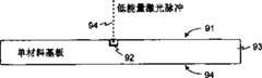
在本发明中的另外一个实施例中,如图5所示,激光束54的低能量激光脉冲被用在沿着切割线(lane)55的前几个通路中来防止在从晶片50的有源器件(active device)侧加工时穿过有源器件51扩展的大裂缝的发展,如图5(i)a中所示。在激光切割的材料深度约相当于有源器件层的厚度后,激光束54的脉冲能量E在激光切割方案文件的控制下可增加到更高的激光束541的脉冲能量,如图5(i)b中所示,以便更快地加工晶片50的半导体基板53的主体,其由初始加工所加热,这样在加工基板53中的热冲击效应被减弱。当从与承载有源器件51一侧相反的晶片基板53的后侧加工时,如图5(ii)a所示,可以采用一个相似的过程来防止向下切入基板材料的初始激光所产生的裂缝扩展,并且最初使用具有低激光脉冲能量的激光束54。在半导体基板53的主体中,激光能量在激光切割方案文件的控制下增加以使用更高能量激光束541来更快地加工,见图5(ii)b。当从晶片50的后侧加工的激光束541达到包含有源器件51的区域时,激光束54的激光脉冲能量在激光切割方案文件的控制下被减弱以防止对该区域的过分损伤,见图5(ii)c。为了按照此种方式控制激光加工,激光切割方案文件还包括代表分别通过有源层和基板剩余部分所需的扫描数目的数据,以及将基板的温度升高到一个热冲击效应在升高的温度和升高的脉冲能量下不明显的温度所需的初始扫描的数目的数据。In another embodiment of the present invention, as shown in FIG. 5 , low-energy laser pulses of the laser beam 54 are used in the first few passes along the cutting line (lane) 55 to prevent any damage from the wafer 50. The development of a large crack extending through the active device 51 during processing on the active device side, as shown in Figure 5(i)a. After the material depth of the laser cutting is approximately equivalent to the thickness of the active device layer, the pulse energy E of the laser beam 54 can be increased to a higher pulse energy of the
在本发明的另一个实施方式中,如图9所示,在用多通路切割来加工,例如,单层基板93中的例如沟槽或切割线92时,在一个或几个初始通路期间,使用比切割基板主体时所用的激光束941脉冲能量更低的激光束94,来防止在从其加工基板93的第一表面91上的表面微裂纹的产生或至少减少到低于可能在其它情况下发生的程度。相似地,激光束942的最终通路的能量可以减小到用来切割基板93的主体所用的能量以下,来防止与第一表面91相对的基板的第二表面94的或,例如,在沟槽的基底的碎屑或裂纹的产生,或至少将其减少到低于可能在其它情况下发生的程度。在基板93的主体中,使用更高能量的脉冲来有效地切除材料。该脉冲能量可以随着加工深度的增加而增加来更有效地加速材料的切除。In another embodiment of the present invention, as shown in FIG. 9, when multi-pass dicing is used to process, for example, grooves or cut
此外,参考图10,在基板103的加工整个过程中可以改变激光束104的能量以有利于去除加工中产生的碎片109。也就是说,激光束104更高的峰值功率被用在基板深处而不是接近基板表面处。In addition, referring to FIG. 10 , the energy of the laser beam 104 can be varied throughout the processing of the
激光切割模片的机械模片强度为连续激光脉冲之间的空间重叠的函数。连续激光脉冲之间的空间重叠被由此优选地选择来产生从被加工基板获得模片的最佳机械模片强度。例如,用一个355nm的Q开关激光加工的硅基板的机械模片强度的相关性在图6中表示,其中,绘制压力测试的生存可能性为纵坐标,施加在模片上的压力作为横坐标,来用于从30%到76%的一系列脉冲重叠。显然,在这种情况下,具有最高模片强度的曲线61对于30%的脉冲重叠获得。显而易见的是如果激光脉冲重叠过高则一个区域中会有过多的热量,和过多的裂纹。如果脉冲重叠较低,在一个区域中就会有较少的热损伤和较少的裂纹。在实践中,提供所需的模片强度和产量的适当重叠可以由实验确定并存储在激光切割方案文件中用来在加工期间使用。应该理解的是激光脉冲的空间重叠实际上是扫描速率、脉冲重复率和入射激光束的直径的函数,因此仅这些参数需要被存储在激光切割方案文件中。The mechanical die strength of the laser cut die is a function of the spatial overlap between successive laser pulses. The spatial overlap between successive laser pulses is thus preferably chosen to produce an optimum mechanical die strength for obtaining die from the processed substrate. For example, the dependence of mechanical die strength on a silicon substrate processed by a 355 nm Q-switched laser is shown in Figure 6, where the stress test survival probability is plotted as the ordinate and the stress applied on the die as the abscissa, for a range of pulse overlaps from 30% to 76%. Obviously, in this case the
当远心透镜被用来聚焦激光束时,所接受的激光的强度在远心透镜的视野范围内改变。激光参数可以根据聚焦扫描透镜目标的视野范围内的焦点的位置来进行改变以便在整个视野内的工件表面维持恒定的功率密度。作为入射激光强度的一个百分比的透射激光强度在典型远心扫描透镜视野范围内的变化用等值线(contour plot)20在图2的上半部示出。该等值线可以通过在远心透镜下方在基板或工件要位于其中的平面内放置激光功率表来获得。激光功率读数被记录在横跨透镜(典型的40mm×40mm)视野范围内的许多位置上,然后绘制为二维表面图表。激光功率密度图中的不规则主要是由于透镜上抗反射涂层的质量。一个远心透镜包括许多透镜,在任何这些透镜之上的涂层厚度或质量上的任何不规则都可以引起激光功率密度图上可观察到的不规则。而且,由于远心透镜的几何形状,它的固有性能在视野的边缘并不好,因此激光功率密度就会由于远心透镜本身所造成的激光束轮廓的畸变而被减少。When a telecentric lens is used to focus a laser beam, the intensity of the received laser light changes within the field of view of the telecentric lens. Laser parameters may be varied according to the position of the focal point within the field of view of the focused scan lens target in order to maintain a constant power density across the workpiece surface within the field of view. The variation of transmitted laser intensity as a percentage of incident laser intensity over the field of view of a typical telecentric scan lens is shown by
在整个扫描透镜的视野内维持一个恒定的功率密度需要改变激光脉冲能量和激光重复频率之中的至少一个。在本发明的一种实施方式中,激光参数根据聚焦对象视野中的焦点位置来改变,以在横跨整个视野的工件表面维持一个恒定的功率密度。作为入射激光强度的一定百分比的透射激光强度在典型的远心扫描透镜的视野范围上的变化在图2中表示。横跨整个扫描透镜的视野范围维持一个恒定的功率密度需要改变激光脉冲能量和激光重复率之中的至少一个并方便地在固定的激光重复频率下改变激光脉冲能量,或可替换地,在一个固定激光脉冲能量下改变激光重复频率。功率密度(φ)被定义为在激光焦点上单位面积(A单位为平方厘米)上的功率(P单位为瓦特)且由下式给出Maintaining a constant power density across the field of view of the scan lens requires varying at least one of the laser pulse energy and the laser repetition rate. In one embodiment of the invention, laser parameters are varied according to the focus position within the field of view of the focused object to maintain a constant power density across the workpiece surface across the entire field of view. The variation of transmitted laser intensity as a percentage of incident laser intensity over the field of view of a typical telecentric scan lens is shown in FIG. 2 . Maintaining a constant power density across the field of view of the scan lens requires varying at least one of the laser pulse energy and the laser repetition rate and conveniently varying the laser pulse energy at a fixed laser repetition rate, or alternatively, at a The laser repetition rate was changed under a fixed laser pulse energy. The power density (φ) is defined as the power (P in watts) per unit area (A in square centimeters) at the laser focus and is given by
其中功率为每秒(s)的脉冲能量(E单位为焦耳)where the power is the pulse energy per second (s) (E is in joules)
举例说明,图2中的下一半,其脉冲能量作为纵坐标相对于沿着线21的距离,它距离如图2中的上半部分所示的视野的下边缘10mm,在扫描横跨扫描透镜的视野范围的激光来补偿通过远心透镜透射的激光强度的变化时,展示了在基板上维持恒定功率密度所需的激光脉冲能量的修正。在该实施例中,激光沿着长为40mm,距离透镜中心为10mm的直线21扫描。在图2的上半部分,透镜的视野被分成多个区域,其中在所给区域中每个点上的密度为该区域上所有点的±5%以内。对于在本实施例中激光所扫描的40mm的线21,对应扫描线2l的六个部分22,23,24,25,26,27的六个不同区域,被穿过且因此在激光切割方案文件的控制下改变激光能量五次。该激光脉冲能量在区域1中以E4的值221开始用于扫描线21的第一部分22。在区域1的工件的透射激光强度为入射在扫描透镜上的激光强度的80%到85%,且由于区域1代表了与区域2到6相比最低的入射激光强度的区域,因此区域1中每个激光脉冲E4的能量为最高。随着激光从区域1到区域2的扫描,对应扫描线21的第二部分23,该透射的激光强度增加到扫描透镜上入射的激光强度的85%到90%,并为了在工件表面维持一个恒定的功率密度,激光脉冲能量当前减少到E3的值231,其中E3比E4能量上低5%。随着激光束从一个区域横穿到下一个区域,激光脉冲的能量在激光切割方案文件的控制下“实时(on the fly)”改变,(如需要则在脉冲间基线(pulse-to-pulse basis)上)以便在沿着切割路线21的整个40mm长度的工件表面上维持一个恒定的功率密度值(φ)。By way of example, the lower half of Figure 2 has pulse energy as the ordinate relative to the distance along line 21, which is 10 mm from the lower edge of the field of view shown in the upper half of Figure 2, at scans across the scan lens The modification of the laser pulse energy required to maintain a constant power density on a substrate is demonstrated when compensating for variations in laser intensity transmitted through a telecentric lens with a field of view of the laser. In this embodiment, the laser is scanned along a line 21 with a length of 40 mm and a distance of 10 mm from the center of the lens. In the upper half of Figure 2, the field of view of the lens is divided into regions where the density at each point in a given region is within ±5% of all points in that region. For the 40 mm line 21 scanned by the laser in this embodiment, six different areas corresponding to the six parts 22, 23, 24, 25, 26, 27 of the scanned line 21 are passed through and thus in the laser cutting scheme file Change the laser energy five times under the control. This laser pulse energy is used in the first part 22 of the scanning line 21 starting at the value 221 of E4 in the region 1 . The transmitted laser intensity of the workpiece in region 1 is 80% to 85% of the laser intensity incident on the scan lens, and since region 1 represents the region with the lowest incident laser intensity compared to regions 2 to 6, the The energy of each laser pulseE4 is the highest. As the laser scans from zone 1 to zone 2, corresponding to the second portion 23 of the scan line 21, the transmitted laser intensity increases to 85% to 90% of the incident laser intensity on the scan lens and in order to maintain a At constant power density, the laser pulse energy is currently reduced to a value ofE3 of 231, whereE3 is energetically 5% lower thanE4 . As the laser beam traverses from one area to the next, the energy of the laser pulses is changed "on the fly" under the control of the laser cutting plan file, (pulse-to-pulse baseline if necessary). basis)) in order to maintain a constant power density value (φ) along the entire 40 mm length of the workpiece surface along the cutting path 21.
总之,工件表面的激光功率密度φ与激光脉冲能量E成正比。在工件表面的激光脉冲能量值将与因为在扫描透镜中的衰减而与从激光器直接出现的不同。该等值图以二维列阵的形式存储在与激光的计算机控制相关的计算机存储器中,并且基于针对检流计扫描仪的软件以将激光束放置在视野中,同时的命令发送到激光以如激光切割方案文件中所指示的来改变脉冲重复率和激光脉冲能量。激光功率也可以通过激光头自身中的整体功率仪监测,且激光中的功率的变化可以被补偿。原则上,激光功率可以在工件或基板上被监测而不是存储等值图,但在进行这些的过程中将会有激光功率的损失,且优选地将等值图存储在存储器中。根据本发明,该脉冲重复率和脉冲能量的结合在扫描过程中被控制,该激光脉冲能量E在与远心扫描透镜的透射的反比(indirect proportion)中变化,以为了在扫描透镜的整个视野内的工件表面保持恒定的功率密度。这就允许,例如,切割路线的加工和一致深度的指定沟槽,其中切割路线的深度与功率密度φ成正比。在基板用激光加工的情况下,这样激光将切过基板的整个厚度,在整个切割路线中保持一致的功率密度防止了切割路线的部分切割。在选取和安置的过程中,切割路线的部分切割将留下相邻模片之间的材料,当模片从传送带上选取时,粘连的模片可能分离而导致对模片的损伤,因此显著降低了它们的机械强度。In short, the laser power density φ on the workpiece surface is proportional to the laser pulse energy E. The laser pulse energy value at the workpiece surface will differ from that emerging directly from the laser due to attenuation in the scan lens. This contour map is stored in the computer memory associated with the computer control of the laser in the form of a two-dimensional array and is based on software for the galvanometer scanner to place the laser beam in the field of view while commands are sent to the laser to Vary the pulse repetition rate and laser pulse energy as indicated in the laser cutting protocol document. Laser power can also be monitored by an integral power meter in the laser head itself, and variations in power in the laser can be compensated for. In principle, the laser power could be monitored on the workpiece or substrate instead of storing the contour map, but there would be a loss of laser power in doing so, and the contour map would preferably be stored in memory. According to the invention, the combination of pulse repetition rate and pulse energy is controlled during scanning, the laser pulse energy E being varied in indirect proportion to the transmission of the telecentric scan lens in order to achieve a wide range of pulses over the entire field of view of the scan lens. The inner workpiece surface maintains a constant power density. This allows, for example, the machining of cut lines where the depth of the cut lines is proportional to the power density φ and specified grooves of consistent depth. In the case of substrates being processed with a laser, such that the laser will cut through the entire thickness of the substrate, maintaining a consistent power density throughout the cut path prevents partial cutting of the cut path. During the picking and placement process, partial cutting of the cutting line will leave material between adjacent dies. When the dies are picked from the conveyor belt, the adhered dies may separate and cause damage to the dies, thus significantly reduce their mechanical strength.
根据本发明的激光切割可以在由气体处理系统控制的非环境(non-ambient)空气环境中完成。气体参数比如流速、浓度、温度,气体种类和气体混合可以在激光切割过程之前、之中或之后的至少一个被控制。一系列不同的气体可以被用在激光加工过程之前,之中,或之后的至少一个中。Laser cutting according to the present invention can be accomplished in a non-ambient air environment controlled by a gas handling system. Gas parameters such as flow rate, concentration, temperature, gas species and gas mix can be controlled at least one before, during or after the laser cutting process. A range of different gases can be used at least one of before, during, or after the laser machining process.
一个气体释放头(delivery head)可以用来保证气体一致地被传输到基板的切割区域,这样就完成了一致切割。A gas delivery head can be used to ensure that the gas is uniformly delivered to the cutting area of the substrate, thus achieving a consistent cut.
使用的气体相对于半导体基板和/或半导体晶片或基板中的层可以为惰性或活性的。惰性气体(例如,氩和氦)可以用于在激光加工过程中防止模片壁上氧化层的生长。与硅反应的气体(例如,含氯氟烃和卤化碳)可以用来在激光加工之前,之中和之后的至少一个来通过对基板材料蚀刻减少模片侧壁的表面粗糙度。而且,一个由于激光加工在模片侧墙上产生的热影响区(HAZ)可以用反应气体来蚀刻掉。以这种方式,模片侧壁的质量改善并由此增加了模片的强度。而且,反应气体减少了粘附在模片侧壁上和顶及底表面上的碎片量,这样就减少了激光加工模片上的静电应力点。The gases used may be inert or reactive with respect to the semiconductor substrate and/or layers in the semiconductor wafer or substrate. Inert gases (eg, argon and helium) can be used to prevent the growth of oxide layers on the die walls during laser processing. Gases reactive with silicon (eg, chlorofluorocarbons and halocarbons) can be used to at least one of before, during, and after laser processing to reduce the surface roughness of the sidewalls of the die by etching the substrate material. Also, a heat-affected zone (HAZ) created on the sidewall of the die by laser processing can be etched away with a reactive gas. In this way, the quality of the side walls of the die is improved and thus the strength of the die is increased. Furthermore, the reactive gas reduces the amount of debris that adheres to the sidewalls and top and bottom surfaces of the die, thus reducing electrostatic stress points on the laser processed die.
在本发明的另外一个实施方式中,激光脉冲的能量被减少到与晶片材料的熔化阈值接近的值(在模片切单(singulation)之后)且激光沿着模片的边缘进行扫描来加热(而不是侵蚀)模片侧壁。在此过程中,模片侧壁的表面粗糙度被降低且热影响区的一致性提高,因此导致增强的模片强度。In another embodiment of the invention, the energy of the laser pulse is reduced to a value close to the melting threshold of the wafer material (after die singulation) and the laser is scanned along the edge of the die to heat ( rather than erosion) die sidewalls. In the process, the surface roughness of the sidewalls of the die is reduced and the consistency of the heat-affected zone is improved, thus resulting in enhanced die strength.
在本发明的另外一个实施方式中,激光按照如图7(i)所示的此种方式扫描来为模片71加工圆角72。模片75用传统的机械锯按照图7(ii)中所示的现有技术进行切割。在使用基于激光加工系统的检流计而不是基于切割系统的传统的机械锯时,更容易获得圆角几何形状并更精确。然而,激光脉冲特性必须在圆角部分改变,如典型的情况下,用来引导激光束的检流计扫描镜必须在它们横穿曲线图形时放慢速度。否则,当扫描镜变慢时激光脉冲空间重叠将增加,由此脉冲的间隔时间,Δt,需要增加来在圆角部分维持一个与模片的垂直部分上使用的空间重叠相同的重叠。该数据被存储到激光切割方案文件中来在加工过程中控制激光束。使用激光来生产具有圆角的模片增加了模片的强度并保证了薄晶片的切割。该圆角消除了矩形模片尖角所引起的应力。In another embodiment of the present invention, the laser scans in such a manner as shown in FIG. 7( i ) to process the fillet 72 for the die 71 . Die
而且,加工也可以通过激光切割方案文件和程序控制来控制,这样在模片边缘的角或曲线部分传输的脉冲使得在没有那些可以在模片边缘产生缺陷的过度切割或切割不足的情况下获得“清晰”的拐角或曲线部分。Furthermore, processing can also be controlled by laser cutting profile and program control so that pulses delivered at corners or curves of the die edge are obtained without over-cut or under-cut that can create defects at the die edge. "Sharp" corners or curved sections.
在本发明的另外一个实施方式中,在基板83上用激光束84切割的激光切割路线的锥形85,可以改变来产生凸起的拱形模片侧壁82,如图8所示,以产生一个向着激光束84的方向上呈锥形的切割。在前面说明的实施方式中,这通过在尖角上消除静电应力点导致了增加的模片强度。切割路线侧壁的锥形通过在激光束扫描过基板的过程中改变切割路线的宽度来完成。如图8中所示的锥形侧壁通过在切割路线中随着加工基板深度的增加减少临近激光扫描的数量来完成。In another embodiment of the invention, the taper 85 of the laser cut line 85 cut by the laser beam 84 on the substrate 83 can be altered to produce a raised arched die sidewall 82, as shown in FIG. A conical cut in the direction of the laser beam 84 is produced. In the previously described embodiments, this results in increased die strength by eliminating electrostatic stress points on sharp corners. Tapering of the sidewalls of the cut line is accomplished by varying the width of the cut line as the laser beam scans across the substrate. The tapered sidewalls as shown in Figure 8 are accomplished by decreasing the number of adjacent laser scans in the cutting path as the depth of the processed substrate increases.
如图10所示,一个将要被加工的基板103可以安装在传送带110上,比如在基板103上加工切割路线102来对模片101切单。在此种情况下,该激光束能量可以通过基板来在最终通路中控制以保证不出现对传送带的损伤,如上关于图9(iii)所示。可选择地,或附加地,可以使用一个传送带110,比如聚烯烃基体传送带,其对用来加工基板103的紫外线激光束104基本透明,因此,在加工过程参数的适当选择的情况下,基本不会出现对传送带的损伤。As shown in FIG. 10 , a
本发明并不在限制以上描述的实施方式中,而是可以在构造和细节上变化。The invention is not limited to the embodiments described above but may vary in construction and details.
Claims (52)
Translated fromChineseApplications Claiming Priority (4)
| Application Number | Priority Date | Filing Date | Title |
|---|---|---|---|
| IE20020289 | 2002-04-19 | ||
| IES2002/0289 | 2002-04-19 | ||
| GB0225033.0 | 2002-10-28 | ||
| GB0225033AGB0225033D0 (en) | 2002-10-28 | 2002-10-28 | Program-controlled dicing of a substrate using a pulsed laser |
Publications (1)
| Publication Number | Publication Date |
|---|---|
| CN1663038Atrue CN1663038A (en) | 2005-08-31 |
Family
ID=29252466
Family Applications (1)
| Application Number | Title | Priority Date | Filing Date |
|---|---|---|---|
| CN03814249XAPendingCN1663038A (en) | 2002-04-19 | 2003-04-17 | laser processing |
Country Status (11)
| Country | Link |
|---|---|
| US (4) | US7776720B2 (en) |
| EP (1) | EP1497851B1 (en) |
| JP (1) | JP2005523583A (en) |
| KR (1) | KR101037142B1 (en) |
| CN (1) | CN1663038A (en) |
| AT (1) | ATE316691T1 (en) |
| AU (1) | AU2003224098A1 (en) |
| DE (1) | DE60303371T2 (en) |
| MY (1) | MY134401A (en) |
| TW (1) | TWI227179B (en) |
| WO (1) | WO2003090258A2 (en) |
Cited By (10)
| Publication number | Priority date | Publication date | Assignee | Title |
|---|---|---|---|---|
| CN103582943A (en)* | 2011-06-15 | 2014-02-12 | 应用材料公司 | Multi-step and asymmetrically shaped laser beam scribing |
| CN104541317A (en)* | 2012-08-08 | 2015-04-22 | 住友化学株式会社 | Optical display device production method and optical display device production system |
| CN104684677A (en)* | 2012-09-21 | 2015-06-03 | 伊雷克托科学工业股份有限公司 | Method and apparatus for separation of workpieces and articles produced thereby |
| CN101347869B (en)* | 2007-07-19 | 2015-09-09 | 日东电工株式会社 | Laser processing |
| CN101657292B (en)* | 2006-11-27 | 2016-03-16 | 伊雷克托科学工业股份有限公司 | laser processing |
| CN107430997A (en)* | 2014-12-30 | 2017-12-01 | 苏斯微科光电系统股份有限公司 | For minimizing the laser ablation system for including variable energy beam of etch stop material damage |
| CN114582803A (en)* | 2020-12-02 | 2022-06-03 | 联华电子股份有限公司 | Method for manufacturing semiconductor tube core and semiconductor device |
| CN115835936A (en)* | 2020-07-24 | 2023-03-21 | 应用材料公司 | Laser Ablation Systems for Package Manufacturing |
| CN116117342A (en)* | 2022-10-31 | 2023-05-16 | 武汉新芯集成电路制造有限公司 | Method for cutting substrate by laser and laser cutting device |
| US12374611B2 (en) | 2019-11-27 | 2025-07-29 | Applied Materials, Inc. | Package core assembly and fabrication methods |
Families Citing this family (157)
| Publication number | Priority date | Publication date | Assignee | Title |
|---|---|---|---|---|
| KR101037142B1 (en) | 2002-04-19 | 2011-05-26 | 일렉트로 사이언티픽 인더스트리즈, 아이엔씨 | Program-controlled dicing of substrate using pulse laser |
| GB2404280B (en)* | 2003-07-03 | 2006-09-27 | Xsil Technology Ltd | Die bonding |
| US7238912B2 (en)* | 2003-10-07 | 2007-07-03 | Midwest Research Institute | Wafer characteristics via reflectometry and wafer processing apparatus and method |
| JP4422463B2 (en)* | 2003-11-07 | 2010-02-24 | 株式会社ディスコ | Semiconductor wafer dividing method |
| DE102004039023A1 (en)* | 2004-08-11 | 2006-02-23 | Siemens Ag | Method for processing a workpiece by means of laser radiation, laser processing system |
| EP1630729B1 (en)* | 2004-08-31 | 2007-12-26 | STMicroelectronics S.r.l. | A method for manufacturing a moulded MMC multi media card package obtained with laser cutting |
| CN101036223A (en) | 2004-10-05 | 2007-09-12 | 皇家飞利浦电子股份有限公司 | Method for laser dicing of a substrate |
| GB2420443B (en)* | 2004-11-01 | 2009-09-16 | Xsil Technology Ltd | Increasing die strength by etching during or after dicing |
| JP2006159254A (en)* | 2004-12-07 | 2006-06-22 | Disco Abrasive Syst Ltd | Laser processing equipment |
| JP4908936B2 (en)* | 2005-06-30 | 2012-04-04 | 株式会社半導体エネルギー研究所 | Method for manufacturing semiconductor device |
| JP2007095952A (en)* | 2005-09-28 | 2007-04-12 | Tokyo Seimitsu Co Ltd | Laser dicing equipment and laser dicing method |
| KR100699246B1 (en)* | 2006-04-03 | 2007-03-28 | 주식회사 고려반도체시스템 | Wafer laser sawing device and laser intensity control method |
| SG188829A1 (en)* | 2006-06-08 | 2013-04-30 | Apic Yamada Corp | Semiconductor cutting device, semiconductor cutting method, semiconductor cutting system, laser cutting device and laser cutting method |
| JP2007329359A (en)* | 2006-06-08 | 2007-12-20 | Apic Yamada Corp | System and method for cutting semiconductor |
| JP2007329358A (en)* | 2006-06-08 | 2007-12-20 | Apic Yamada Corp | System and method for cutting semiconductor |
| TWI298280B (en) | 2006-09-06 | 2008-07-01 | Nat Applied Res Laboratories | Method for cutting non-metal material |
| KR100817823B1 (en)* | 2006-11-22 | 2008-03-31 | 주식회사 이오테크닉스 | How to Cut a Memory Card Board |
| US7648891B2 (en)* | 2006-12-22 | 2010-01-19 | International Business Machines Corporation | Semiconductor chip shape alteration |
| US20080220590A1 (en)* | 2007-03-06 | 2008-09-11 | Texas Instruments Incorporated | Thin wafer dicing using UV laser |
| JP5142565B2 (en)* | 2007-03-20 | 2013-02-13 | 三洋電機株式会社 | Manufacturing method of solar cell |
| WO2008141118A1 (en)* | 2007-05-10 | 2008-11-20 | Linde, Inc. | Laser activated fluorine treatment of silicon substrates |
| US8067256B2 (en)* | 2007-09-28 | 2011-11-29 | Intel Corporation | Method of making microelectronic package using integrated heat spreader stiffener panel and microelectronic package formed according to the method |
| JP5160868B2 (en)* | 2007-12-06 | 2013-03-13 | 株式会社ディスコ | Method for forming a modified layer on a substrate |
| JP5024118B2 (en)* | 2008-02-29 | 2012-09-12 | 住友電気工業株式会社 | Laser oscillation method, laser, laser processing method, and laser measurement method |
| GB2458475B (en)* | 2008-03-18 | 2011-10-26 | Xsil Technology Ltd | Processing of multilayer semiconductor wafers |
| WO2009117451A1 (en)* | 2008-03-21 | 2009-09-24 | Imra America, Inc. | Laser-based material processing methods and systems |
| US8426250B2 (en)* | 2008-10-22 | 2013-04-23 | Intel Corporation | Laser-assisted chemical singulation of a wafer |
| US20100129984A1 (en)* | 2008-11-26 | 2010-05-27 | George Vakanas | Wafer singulation in high volume manufacturing |
| US10307862B2 (en) | 2009-03-27 | 2019-06-04 | Electro Scientific Industries, Inc | Laser micromachining with tailored bursts of short laser pulses |
| DE102009026410A1 (en)* | 2009-05-20 | 2011-03-17 | Carl Baasel Lasertechnik Gmbh & Co. Kg | Method for separating silicon solar cells |
| JP5473414B2 (en)* | 2009-06-10 | 2014-04-16 | 株式会社ディスコ | Laser processing equipment |
| US8444850B2 (en)* | 2009-08-17 | 2013-05-21 | Exxonmobil Research And Engineering Company | Operating method for hydrodenitrogenation |
| US8378458B2 (en)* | 2010-03-22 | 2013-02-19 | Advanced Micro Devices, Inc. | Semiconductor chip with a rounded corner |
| KR20110114028A (en)* | 2010-04-12 | 2011-10-19 | 삼성전자주식회사 | Specimen Processing Apparatus and Method |
| TW201134596A (en)* | 2010-04-15 | 2011-10-16 | Epileds Technologies Inc | Laser processing method |
| CN102218607B (en)* | 2010-04-15 | 2014-11-05 | 鸿富锦精密工业(深圳)有限公司 | Pulse laser cutting method of bulk amorphous alloy |
| US8642448B2 (en) | 2010-06-22 | 2014-02-04 | Applied Materials, Inc. | Wafer dicing using femtosecond-based laser and plasma etch |
| KR20140018183A (en)* | 2010-09-16 | 2014-02-12 | 레이디안스, 아이엔씨. | Laser based processing of layered materials |
| US9023461B2 (en)* | 2010-10-21 | 2015-05-05 | Electro Scientific Industries, Inc. | Apparatus for optically laser marking articles |
| JP5839383B2 (en)* | 2011-03-18 | 2016-01-06 | 株式会社ディスコ | Wafer processing method |
| US8912077B2 (en) | 2011-06-15 | 2014-12-16 | Applied Materials, Inc. | Hybrid laser and plasma etch wafer dicing using substrate carrier |
| US9029242B2 (en) | 2011-06-15 | 2015-05-12 | Applied Materials, Inc. | Damage isolation by shaped beam delivery in laser scribing process |
| US8507363B2 (en) | 2011-06-15 | 2013-08-13 | Applied Materials, Inc. | Laser and plasma etch wafer dicing using water-soluble die attach film |
| US9126285B2 (en) | 2011-06-15 | 2015-09-08 | Applied Materials, Inc. | Laser and plasma etch wafer dicing using physically-removable mask |
| US8557682B2 (en)* | 2011-06-15 | 2013-10-15 | Applied Materials, Inc. | Multi-layer mask for substrate dicing by laser and plasma etch |
| US9129904B2 (en) | 2011-06-15 | 2015-09-08 | Applied Materials, Inc. | Wafer dicing using pulse train laser with multiple-pulse bursts and plasma etch |
| US8598016B2 (en) | 2011-06-15 | 2013-12-03 | Applied Materials, Inc. | In-situ deposited mask layer for device singulation by laser scribing and plasma etch |
| US8703581B2 (en) | 2011-06-15 | 2014-04-22 | Applied Materials, Inc. | Water soluble mask for substrate dicing by laser and plasma etch |
| US8759197B2 (en)* | 2011-06-15 | 2014-06-24 | Applied Materials, Inc. | Multi-step and asymmetrically shaped laser beam scribing |
| US8673741B2 (en) | 2011-06-24 | 2014-03-18 | Electro Scientific Industries, Inc | Etching a laser-cut semiconductor before dicing a die attach film (DAF) or other material layer |
| US8951819B2 (en) | 2011-07-11 | 2015-02-10 | Applied Materials, Inc. | Wafer dicing using hybrid split-beam laser scribing process with plasma etch |
| US8399281B1 (en)* | 2011-08-31 | 2013-03-19 | Alta Devices, Inc. | Two beam backside laser dicing of semiconductor films |
| US8361828B1 (en)* | 2011-08-31 | 2013-01-29 | Alta Devices, Inc. | Aligned frontside backside laser dicing of semiconductor films |
| DE102011054891B4 (en)* | 2011-10-28 | 2017-10-19 | Osram Opto Semiconductors Gmbh | Method for severing a semiconductor device composite |
| US8940618B2 (en)* | 2012-03-13 | 2015-01-27 | Taiwan Semiconductor Manufacturing Company, Ltd. | Method and device for cutting semiconductor wafers |
| CN102615281B (en)* | 2012-04-09 | 2013-10-16 | 西安交通大学 | Regional mobile light source scanning system for laser rapid prototyping technology |
| US8652940B2 (en) | 2012-04-10 | 2014-02-18 | Applied Materials, Inc. | Wafer dicing used hybrid multi-step laser scribing process with plasma etch |
| US8946057B2 (en) | 2012-04-24 | 2015-02-03 | Applied Materials, Inc. | Laser and plasma etch wafer dicing using UV-curable adhesive film |
| JP5442801B2 (en)* | 2012-05-14 | 2014-03-12 | アピックヤマダ株式会社 | Semiconductor cutting apparatus and semiconductor cutting method |
| US9266192B2 (en) | 2012-05-29 | 2016-02-23 | Electro Scientific Industries, Inc. | Method and apparatus for processing workpieces |
| US8969177B2 (en) | 2012-06-29 | 2015-03-03 | Applied Materials, Inc. | Laser and plasma etch wafer dicing with a double sided UV-curable adhesive film |
| US9048309B2 (en) | 2012-07-10 | 2015-06-02 | Applied Materials, Inc. | Uniform masking for wafer dicing using laser and plasma etch |
| US8993414B2 (en) | 2012-07-13 | 2015-03-31 | Applied Materials, Inc. | Laser scribing and plasma etch for high die break strength and clean sidewall |
| US8859397B2 (en) | 2012-07-13 | 2014-10-14 | Applied Materials, Inc. | Method of coating water soluble mask for laser scribing and plasma etch |
| US8845854B2 (en) | 2012-07-13 | 2014-09-30 | Applied Materials, Inc. | Laser, plasma etch, and backside grind process for wafer dicing |
| US8940619B2 (en) | 2012-07-13 | 2015-01-27 | Applied Materials, Inc. | Method of diced wafer transportation |
| CN103568139A (en)* | 2012-07-18 | 2014-02-12 | 飞思卡尔半导体公司 | Semiconductor chip dicing method |
| US9159574B2 (en) | 2012-08-27 | 2015-10-13 | Applied Materials, Inc. | Method of silicon etch for trench sidewall smoothing |
| US9252057B2 (en) | 2012-10-17 | 2016-02-02 | Applied Materials, Inc. | Laser and plasma etch wafer dicing with partial pre-curing of UV release dicing tape for film frame wafer application |
| US8975162B2 (en) | 2012-12-20 | 2015-03-10 | Applied Materials, Inc. | Wafer dicing from wafer backside |
| US9236305B2 (en) | 2013-01-25 | 2016-01-12 | Applied Materials, Inc. | Wafer dicing with etch chamber shield ring for film frame wafer applications |
| US8980726B2 (en) | 2013-01-25 | 2015-03-17 | Applied Materials, Inc. | Substrate dicing by laser ablation and plasma etch damage removal for ultra-thin wafers |
| US9919380B2 (en) | 2013-02-23 | 2018-03-20 | Coherent, Inc. | Shaping of brittle materials with controlled surface and bulk properties |
| TWI619165B (en) | 2013-03-14 | 2018-03-21 | 應用材料股份有限公司 | Multi-layer mask with non-light definable laser energy absorbing layer for substrate cutting by laser and plasma etching |
| US20140263211A1 (en)* | 2013-03-15 | 2014-09-18 | Apple Inc. | Methods for Trimming Display Polarizers Using Lasers |
| US11233029B2 (en) | 2013-04-10 | 2022-01-25 | Mitsubishi Electric Corporation | Semiconductor device having a device fixed on a substrate with an adhesive |
| US8883614B1 (en) | 2013-05-22 | 2014-11-11 | Applied Materials, Inc. | Wafer dicing with wide kerf by laser scribing and plasma etching hybrid approach |
| DE102013212577A1 (en)* | 2013-06-28 | 2014-12-31 | Trumpf Laser- Und Systemtechnik Gmbh | Method for cutting off a workpiece by means of a pulsed laser beam |
| US9105710B2 (en) | 2013-08-30 | 2015-08-11 | Applied Materials, Inc. | Wafer dicing method for improving die packaging quality |
| US9224650B2 (en) | 2013-09-19 | 2015-12-29 | Applied Materials, Inc. | Wafer dicing from wafer backside and front side |
| US9460966B2 (en) | 2013-10-10 | 2016-10-04 | Applied Materials, Inc. | Method and apparatus for dicing wafers having thick passivation polymer layer |
| US9349645B2 (en)* | 2013-10-16 | 2016-05-24 | Nxp B.V. | Apparatus, device and method for wafer dicing |
| KR102103502B1 (en)* | 2013-10-21 | 2020-04-23 | 삼성디스플레이 주식회사 | Method for cutting substrate |
| US9041198B2 (en) | 2013-10-22 | 2015-05-26 | Applied Materials, Inc. | Maskless hybrid laser scribing and plasma etching wafer dicing process |
| US9312177B2 (en) | 2013-12-06 | 2016-04-12 | Applied Materials, Inc. | Screen print mask for laser scribe and plasma etch wafer dicing process |
| US9299614B2 (en) | 2013-12-10 | 2016-03-29 | Applied Materials, Inc. | Method and carrier for dicing a wafer |
| US9293304B2 (en) | 2013-12-17 | 2016-03-22 | Applied Materials, Inc. | Plasma thermal shield for heat dissipation in plasma chamber |
| US9012305B1 (en) | 2014-01-29 | 2015-04-21 | Applied Materials, Inc. | Wafer dicing using hybrid laser scribing and plasma etch approach with intermediate non-reactive post mask-opening clean |
| US9018079B1 (en) | 2014-01-29 | 2015-04-28 | Applied Materials, Inc. | Wafer dicing using hybrid laser scribing and plasma etch approach with intermediate reactive post mask-opening clean |
| US9299611B2 (en) | 2014-01-29 | 2016-03-29 | Applied Materials, Inc. | Method of wafer dicing using hybrid laser scribing and plasma etch approach with mask plasma treatment for improved mask etch resistance |
| US8927393B1 (en) | 2014-01-29 | 2015-01-06 | Applied Materials, Inc. | Water soluble mask formation by dry film vacuum lamination for laser and plasma dicing |
| US9236284B2 (en) | 2014-01-31 | 2016-01-12 | Applied Materials, Inc. | Cooled tape frame lift and low contact shadow ring for plasma heat isolation |
| US8991329B1 (en) | 2014-01-31 | 2015-03-31 | Applied Materials, Inc. | Wafer coating |
| JP6250429B2 (en)* | 2014-02-13 | 2017-12-20 | エスアイアイ・セミコンダクタ株式会社 | Semiconductor device and manufacturing method thereof |
| US9130030B1 (en) | 2014-03-07 | 2015-09-08 | Applied Materials, Inc. | Baking tool for improved wafer coating process |
| US20150255349A1 (en) | 2014-03-07 | 2015-09-10 | JAMES Matthew HOLDEN | Approaches for cleaning a wafer during hybrid laser scribing and plasma etching wafer dicing processes |
| US9275902B2 (en) | 2014-03-26 | 2016-03-01 | Applied Materials, Inc. | Dicing processes for thin wafers with bumps on wafer backside |
| US9728518B2 (en) | 2014-04-01 | 2017-08-08 | Ati Technologies Ulc | Interconnect etch with polymer layer edge protection |
| US9076860B1 (en) | 2014-04-04 | 2015-07-07 | Applied Materials, Inc. | Residue removal from singulated die sidewall |
| US8975163B1 (en) | 2014-04-10 | 2015-03-10 | Applied Materials, Inc. | Laser-dominated laser scribing and plasma etch hybrid wafer dicing |
| US8932939B1 (en) | 2014-04-14 | 2015-01-13 | Applied Materials, Inc. | Water soluble mask formation by dry film lamination |
| US8912078B1 (en) | 2014-04-16 | 2014-12-16 | Applied Materials, Inc. | Dicing wafers having solder bumps on wafer backside |
| US8999816B1 (en) | 2014-04-18 | 2015-04-07 | Applied Materials, Inc. | Pre-patterned dry laminate mask for wafer dicing processes |
| US8912075B1 (en) | 2014-04-29 | 2014-12-16 | Applied Materials, Inc. | Wafer edge warp supression for thin wafer supported by tape frame |
| US9159621B1 (en) | 2014-04-29 | 2015-10-13 | Applied Materials, Inc. | Dicing tape protection for wafer dicing using laser scribe process |
| US8980727B1 (en) | 2014-05-07 | 2015-03-17 | Applied Materials, Inc. | Substrate patterning using hybrid laser scribing and plasma etching processing schemes |
| US9112050B1 (en) | 2014-05-13 | 2015-08-18 | Applied Materials, Inc. | Dicing tape thermal management by wafer frame support ring cooling during plasma dicing |
| US9034771B1 (en) | 2014-05-23 | 2015-05-19 | Applied Materials, Inc. | Cooling pedestal for dicing tape thermal management during plasma dicing |
| US9666522B2 (en)* | 2014-05-29 | 2017-05-30 | Taiwan Semiconductor Manufacturing Company, Ltd. | Alignment mark design for packages |
| US9142459B1 (en) | 2014-06-30 | 2015-09-22 | Applied Materials, Inc. | Wafer dicing using hybrid laser scribing and plasma etch approach with mask application by vacuum lamination |
| US9130057B1 (en) | 2014-06-30 | 2015-09-08 | Applied Materials, Inc. | Hybrid dicing process using a blade and laser |
| US9093518B1 (en) | 2014-06-30 | 2015-07-28 | Applied Materials, Inc. | Singulation of wafers having wafer-level underfill |
| US9165832B1 (en) | 2014-06-30 | 2015-10-20 | Applied Materials, Inc. | Method of die singulation using laser ablation and induction of internal defects with a laser |
| US9349648B2 (en) | 2014-07-22 | 2016-05-24 | Applied Materials, Inc. | Hybrid wafer dicing approach using a rectangular shaped two-dimensional top hat laser beam profile or a linear shaped one-dimensional top hat laser beam profile laser scribing process and plasma etch process |
| US9117868B1 (en) | 2014-08-12 | 2015-08-25 | Applied Materials, Inc. | Bipolar electrostatic chuck for dicing tape thermal management during plasma dicing |
| US9196498B1 (en) | 2014-08-12 | 2015-11-24 | Applied Materials, Inc. | Stationary actively-cooled shadow ring for heat dissipation in plasma chamber |
| US9281244B1 (en) | 2014-09-18 | 2016-03-08 | Applied Materials, Inc. | Hybrid wafer dicing approach using an adaptive optics-controlled laser scribing process and plasma etch process |
| US11195756B2 (en) | 2014-09-19 | 2021-12-07 | Applied Materials, Inc. | Proximity contact cover ring for plasma dicing |
| US9177861B1 (en) | 2014-09-19 | 2015-11-03 | Applied Materials, Inc. | Hybrid wafer dicing approach using laser scribing process based on an elliptical laser beam profile or a spatio-temporal controlled laser beam profile |
| US9196536B1 (en) | 2014-09-25 | 2015-11-24 | Applied Materials, Inc. | Hybrid wafer dicing approach using a phase modulated laser beam profile laser scribing process and plasma etch process |
| US9130056B1 (en) | 2014-10-03 | 2015-09-08 | Applied Materials, Inc. | Bi-layer wafer-level underfill mask for wafer dicing and approaches for performing wafer dicing |
| US9245803B1 (en) | 2014-10-17 | 2016-01-26 | Applied Materials, Inc. | Hybrid wafer dicing approach using a bessel beam shaper laser scribing process and plasma etch process |
| US10692765B2 (en) | 2014-11-07 | 2020-06-23 | Applied Materials, Inc. | Transfer arm for film frame substrate handling during plasma singulation of wafers |
| US9159624B1 (en) | 2015-01-05 | 2015-10-13 | Applied Materials, Inc. | Vacuum lamination of polymeric dry films for wafer dicing using hybrid laser scribing and plasma etch approach |
| US9330977B1 (en) | 2015-01-05 | 2016-05-03 | Applied Materials, Inc. | Hybrid wafer dicing approach using a galvo scanner and linear stage hybrid motion laser scribing process and plasma etch process |
| US9355907B1 (en) | 2015-01-05 | 2016-05-31 | Applied Materials, Inc. | Hybrid wafer dicing approach using a line shaped laser beam profile laser scribing process and plasma etch process |
| US9601375B2 (en) | 2015-04-27 | 2017-03-21 | Applied Materials, Inc. | UV-cure pre-treatment of carrier film for wafer dicing using hybrid laser scribing and plasma etch approach |
| US9478455B1 (en) | 2015-06-12 | 2016-10-25 | Applied Materials, Inc. | Thermal pyrolytic graphite shadow ring assembly for heat dissipation in plasma chamber |
| US9721839B2 (en) | 2015-06-12 | 2017-08-01 | Applied Materials, Inc. | Etch-resistant water soluble mask for hybrid wafer dicing using laser scribing and plasma etch |
| KR102698971B1 (en) | 2015-08-26 | 2024-08-27 | 일렉트로 싸이언티픽 인더스트리이즈 인코포레이티드 | Laser scan sequencing and direction for gas flow |
| WO2017082210A1 (en)* | 2015-11-09 | 2017-05-18 | 古河電気工業株式会社 | Method for manufacturing semiconductor chip, and mask-integrated surface protection tape used therein |
| BR112018010732B1 (en)* | 2015-12-18 | 2022-08-23 | Kimberly-Clark Worldwide, Inc | METHOD OF CUTTING A BLANKET STRUCTURE |
| US9972575B2 (en) | 2016-03-03 | 2018-05-15 | Applied Materials, Inc. | Hybrid wafer dicing approach using a split beam laser scribing process and plasma etch process |
| JP6666173B2 (en)* | 2016-03-09 | 2020-03-13 | 株式会社ディスコ | Laser processing equipment |
| US9852997B2 (en) | 2016-03-25 | 2017-12-26 | Applied Materials, Inc. | Hybrid wafer dicing approach using a rotating beam laser scribing process and plasma etch process |
| US9793132B1 (en) | 2016-05-13 | 2017-10-17 | Applied Materials, Inc. | Etch mask for hybrid laser scribing and plasma etch wafer singulation process |
| KR102691911B1 (en)* | 2016-12-22 | 2024-08-07 | 삼성디스플레이 주식회사 | Flexible display panel, method for manufacturing flexible display panel, and apparatus for manufacturing flexible display panel |
| JP6831248B2 (en)* | 2017-01-16 | 2021-02-17 | 株式会社ディスコ | Wafer processing method and adhesive tape |
| US11158540B2 (en) | 2017-05-26 | 2021-10-26 | Applied Materials, Inc. | Light-absorbing mask for hybrid laser scribing and plasma etch wafer singulation process |
| US10363629B2 (en) | 2017-06-01 | 2019-07-30 | Applied Materials, Inc. | Mitigation of particle contamination for wafer dicing processes |
| US10535561B2 (en) | 2018-03-12 | 2020-01-14 | Applied Materials, Inc. | Hybrid wafer dicing approach using a multiple pass laser scribing process and plasma etch process |
| US20190363018A1 (en) | 2018-05-24 | 2019-11-28 | Semiconductor Components Industries, Llc | Die cleaning systems and related methods |
| US11355394B2 (en) | 2018-09-13 | 2022-06-07 | Applied Materials, Inc. | Wafer dicing using hybrid laser scribing and plasma etch approach with intermediate breakthrough treatment |
| DE102018217526A1 (en) | 2018-10-12 | 2020-04-16 | Trumpf Werkzeugmaschinen Gmbh + Co. Kg | Method for determining a parameter of a machining process and machine tool |
| JP2020066015A (en) | 2018-10-23 | 2020-04-30 | 株式会社ディスコ | Laser processing method |
| JP7239298B2 (en)* | 2018-10-23 | 2023-03-14 | 株式会社ディスコ | Laser processing method |
| JP7291501B2 (en)* | 2019-03-11 | 2023-06-15 | 株式会社フジクラ | Laser processing equipment |
| KR102270780B1 (en) | 2019-04-30 | 2021-06-30 | 세메스 주식회사 | Film removing method, substrate processing method, and substrate processing apparatus |
| US11011424B2 (en) | 2019-08-06 | 2021-05-18 | Applied Materials, Inc. | Hybrid wafer dicing approach using a spatially multi-focused laser beam laser scribing process and plasma etch process |
| US11342226B2 (en) | 2019-08-13 | 2022-05-24 | Applied Materials, Inc. | Hybrid wafer dicing approach using an actively-focused laser beam laser scribing process and plasma etch process |
| US10903121B1 (en) | 2019-08-14 | 2021-01-26 | Applied Materials, Inc. | Hybrid wafer dicing approach using a uniform rotating beam laser scribing process and plasma etch process |
| US11600492B2 (en) | 2019-12-10 | 2023-03-07 | Applied Materials, Inc. | Electrostatic chuck with reduced current leakage for hybrid laser scribing and plasma etch wafer singulation process |
| US11211247B2 (en) | 2020-01-30 | 2021-12-28 | Applied Materials, Inc. | Water soluble organic-inorganic hybrid mask formulations and their applications |
| KR102786594B1 (en) | 2020-05-04 | 2025-03-26 | 삼성전자주식회사 | semiconductor package and method for manufacturing the same |
| KR102840349B1 (en) | 2020-07-14 | 2025-07-30 | 삼성전자주식회사 | semiconductor package |
| CN114178710B (en) | 2020-08-24 | 2024-11-26 | 奥特斯(中国)有限公司 | Component carrier and method for manufacturing the same |
| US20250033345A1 (en)* | 2023-07-27 | 2025-01-30 | Fmc Technologies, Inc. | Systems and methods for joining composite structures to metal structures |
Family Cites Families (58)
| Publication number | Priority date | Publication date | Assignee | Title |
|---|---|---|---|---|
| US3866398A (en)* | 1973-12-20 | 1975-02-18 | Texas Instruments Inc | In-situ gas-phase reaction for removal of laser-scribe debris |
| US4190488A (en) | 1978-08-21 | 1980-02-26 | International Business Machines Corporation | Etching method using noble gas halides |
| JPS56103447A (en) | 1980-01-22 | 1981-08-18 | Toshiba Corp | Dicing method of semiconductor wafer |
| US4355457A (en) | 1980-10-29 | 1982-10-26 | Rca Corporation | Method of forming a mesa in a semiconductor device with subsequent separation into individual devices |
| US4399345A (en) | 1981-06-09 | 1983-08-16 | Analog Devices, Inc. | Laser trimming of circuit elements on semiconductive substrates |
| US4478677A (en) | 1983-12-22 | 1984-10-23 | International Business Machines Corporation | Laser induced dry etching of vias in glass with non-contact masking |
| US4639572A (en)* | 1985-11-25 | 1987-01-27 | Ibm Corporation | Laser cutting of composite materials |
| US5322988A (en)* | 1990-03-29 | 1994-06-21 | The United States Of America As Represented By The Secretary Of The Navy | Laser texturing |
| JPH05291398A (en)* | 1992-04-08 | 1993-11-05 | Sony Corp | Manufacture of element substrate and liquid crystal display device |
| US5265114C1 (en) | 1992-09-10 | 2001-08-21 | Electro Scient Ind Inc | System and method for selectively laser processing a target structure of one or more materials of a multimaterial multilayer device |
| JPH06238478A (en) | 1993-02-15 | 1994-08-30 | Nippon Steel Corp | Laser beam welding method for thick metal plates |
| US5685995A (en) | 1994-11-22 | 1997-11-11 | Electro Scientific Industries, Inc. | Method for laser functional trimming of films and devices |
| US6969635B2 (en) | 2000-12-07 | 2005-11-29 | Reflectivity, Inc. | Methods for depositing, releasing and packaging micro-electromechanical devices on wafer substrates |
| KR970008386A (en)* | 1995-07-07 | 1997-02-24 | 하라 세이지 | A method of dividing a substrate and a dividing device |
| US6498074B2 (en) | 1996-10-29 | 2002-12-24 | Tru-Si Technologies, Inc. | Thinning and dicing of semiconductor wafers using dry etch, and obtaining semiconductor chips with rounded bottom edges and corners |
| GB2320615B (en) | 1996-12-19 | 2001-06-20 | Lintec Corp | Process for producing a chip and pressure sensitive adhesive sheet for said process |
| US6162367A (en) | 1997-01-22 | 2000-12-19 | California Institute Of Technology | Gas-phase silicon etching with bromine trifluoride |
| JP2000031115A (en) | 1998-06-29 | 2000-01-28 | Lucent Technol Inc | Method for forming chip from wafer |
| KR100283415B1 (en)* | 1998-07-29 | 2001-06-01 | 구자홍 | Method and apparatus of machining a transparent medium by laser |
| JP2000091274A (en) | 1998-09-17 | 2000-03-31 | Hitachi Ltd | Method for forming semiconductor chip and method for manufacturing semiconductor device using the same |
| JP2000114204A (en) | 1998-10-01 | 2000-04-21 | Mitsubishi Electric Corp | Wafer sheet, method of manufacturing semiconductor device using the same, and semiconductor manufacturing apparatus |
| US6413839B1 (en) | 1998-10-23 | 2002-07-02 | Emcore Corporation | Semiconductor device separation using a patterned laser projection |
| JP3447602B2 (en) | 1999-02-05 | 2003-09-16 | シャープ株式会社 | Method for manufacturing semiconductor device |
| DE19919471A1 (en) | 1999-04-29 | 2000-11-09 | Bosch Gmbh Robert | Process for eliminating defects in silicon bodies by selective etching |
| EP1099183A4 (en)* | 1999-05-24 | 2004-12-15 | Potomac Photonics Inc | Material delivery system for miniature structure fabrication |
| US6792326B1 (en)* | 1999-05-24 | 2004-09-14 | Potomac Photonics, Inc. | Material delivery system for miniature structure fabrication |
| US6420245B1 (en) | 1999-06-08 | 2002-07-16 | Kulicke & Soffa Investments, Inc. | Method for singulating semiconductor wafers |
| JP4387007B2 (en)* | 1999-10-26 | 2009-12-16 | 株式会社ディスコ | Method for dividing semiconductor wafer |
| US6290864B1 (en) | 1999-10-26 | 2001-09-18 | Reflectivity, Inc. | Fluoride gas etching of silicon with improved selectivity |
| US6531681B1 (en) | 2000-03-27 | 2003-03-11 | Ultratech Stepper, Inc. | Apparatus having line source of radiant energy for exposing a substrate |
| JP2002050670A (en)* | 2000-08-04 | 2002-02-15 | Toshiba Corp | Pickup device and pickup method |
| US6676878B2 (en)* | 2001-01-31 | 2004-01-13 | Electro Scientific Industries, Inc. | Laser segmented cutting |
| US7157038B2 (en) | 2000-09-20 | 2007-01-02 | Electro Scientific Industries, Inc. | Ultraviolet laser ablative patterning of microstructures in semiconductors |
| US20020071818A1 (en) | 2000-10-02 | 2002-06-13 | Cole Curtis A. | Skin cleanser containing anti-aging active |
| US6586707B2 (en)* | 2000-10-26 | 2003-07-01 | Xsil Technology Limited | Control of laser machining |
| GB0102154D0 (en) | 2001-01-27 | 2001-03-14 | Ibm | Decimal to binary coder/decoder |
| US6770544B2 (en)* | 2001-02-21 | 2004-08-03 | Nec Machinery Corporation | Substrate cutting method |
| US6465344B1 (en) | 2001-03-09 | 2002-10-15 | Indigo Systems Corporation | Crystal thinning method for improved yield and reliability |
| US8048774B2 (en)* | 2001-10-01 | 2011-11-01 | Electro Scientific Industries, Inc. | Methods and systems for laser machining a substrate |
| US6642127B2 (en) | 2001-10-19 | 2003-11-04 | Applied Materials, Inc. | Method for dicing a semiconductor wafer |
| JP2003197569A (en) | 2001-12-28 | 2003-07-11 | Disco Abrasive Syst Ltd | Method for manufacturing semiconductor chip |
| US20040137700A1 (en) | 2002-02-25 | 2004-07-15 | Kazuma Sekiya | Method for dividing semiconductor wafer |
| WO2003078091A1 (en) | 2002-03-11 | 2003-09-25 | Becton, Dickinson And Company | System and method for the manufacture of surgical blades |
| KR101037142B1 (en) | 2002-04-19 | 2011-05-26 | 일렉트로 사이언티픽 인더스트리즈, 아이엔씨 | Program-controlled dicing of substrate using pulse laser |
| US6817776B2 (en) | 2002-11-19 | 2004-11-16 | International Business Machines Corporation | Method of bonding optical fibers and optical fiber assembly |
| TWI238444B (en) | 2002-12-10 | 2005-08-21 | Seiko Epson Corp | Method for manufacturing optoelectronic device, optoelectronic device and electronic machine |
| JP4474834B2 (en) | 2003-02-27 | 2010-06-09 | セイコーエプソン株式会社 | Manufacturing method of semiconductor chip |
| GB2399311B (en) | 2003-03-04 | 2005-06-15 | Xsil Technology Ltd | Laser machining using an active assist gas |
| US7087452B2 (en) | 2003-04-22 | 2006-08-08 | Intel Corporation | Edge arrangements for integrated circuit chips |
| JP2005051007A (en) | 2003-07-28 | 2005-02-24 | Tokyo Electron Ltd | Manufacturing method of semiconductor chip |
| GB2420443B (en)* | 2004-11-01 | 2009-09-16 | Xsil Technology Ltd | Increasing die strength by etching during or after dicing |
| US7265034B2 (en) | 2005-02-18 | 2007-09-04 | Taiwan Semiconductor Manufacturing Company, Ltd. | Method of cutting integrated circuit chips from wafer by ablating with laser and cutting with saw blade |
| US7638435B2 (en) | 2005-08-23 | 2009-12-29 | Xactix, Inc. | Pulsed etching cooling |
| JP4819513B2 (en) | 2006-01-26 | 2011-11-24 | 株式会社日立国際電気 | Television camera and base station device |
| JP2007273068A (en) | 2006-03-10 | 2007-10-18 | Sony Corp | Hologram recording and reproducing apparatus |
| JP4840174B2 (en)* | 2007-02-08 | 2011-12-21 | パナソニック株式会社 | Manufacturing method of semiconductor chip |
| JP5636226B2 (en) | 2010-08-16 | 2014-12-03 | ルネサスエレクトロニクス株式会社 | Semiconductor integrated circuit and operation method thereof |
| US8652940B2 (en)* | 2012-04-10 | 2014-02-18 | Applied Materials, Inc. | Wafer dicing used hybrid multi-step laser scribing process with plasma etch |
- 2003
- 2003-04-17KRKR1020047016842Apatent/KR101037142B1/ennot_activeExpired - Fee Related
- 2003-04-17AUAU2003224098Apatent/AU2003224098A1/ennot_activeAbandoned
- 2003-04-17EPEP03720496Apatent/EP1497851B1/ennot_activeExpired - Lifetime
- 2003-04-17ATAT03720496Tpatent/ATE316691T1/ennot_activeIP Right Cessation
- 2003-04-17JPJP2003586917Apatent/JP2005523583A/enactivePending
- 2003-04-17USUS10/511,743patent/US7776720B2/ennot_activeExpired - Fee Related
- 2003-04-17WOPCT/EP2003/004069patent/WO2003090258A2/enactiveIP Right Grant
- 2003-04-17DEDE60303371Tpatent/DE60303371T2/ennot_activeExpired - Lifetime
- 2003-04-17CNCN03814249XApatent/CN1663038A/enactivePending
- 2003-04-18MYMYPI20031480Apatent/MY134401A/enunknown
- 2003-04-18TWTW092109096Apatent/TWI227179B/ennot_activeIP Right Cessation
- 2010
- 2010-08-13USUS12/856,374patent/US20110029124A1/ennot_activeAbandoned
- 2012
- 2012-04-17USUS13/448,604patent/US20120264238A1/ennot_activeAbandoned
- 2013
- 2013-09-17USUS14/029,664patent/US9352417B2/ennot_activeExpired - Fee Related
Cited By (14)
| Publication number | Priority date | Publication date | Assignee | Title |
|---|---|---|---|---|
| CN101657292B (en)* | 2006-11-27 | 2016-03-16 | 伊雷克托科学工业股份有限公司 | laser processing |
| CN101347869B (en)* | 2007-07-19 | 2015-09-09 | 日东电工株式会社 | Laser processing |
| CN103582943A (en)* | 2011-06-15 | 2014-02-12 | 应用材料公司 | Multi-step and asymmetrically shaped laser beam scribing |
| CN103582943B (en)* | 2011-06-15 | 2016-08-17 | 应用材料公司 | Multi-step and asymmetrically shaped laser beam scribing |
| CN104541317B (en)* | 2012-08-08 | 2016-11-23 | 住友化学株式会社 | The production method of optical display device and the production system of optical display device |
| CN104541317A (en)* | 2012-08-08 | 2015-04-22 | 住友化学株式会社 | Optical display device production method and optical display device production system |
| CN104684677A (en)* | 2012-09-21 | 2015-06-03 | 伊雷克托科学工业股份有限公司 | Method and apparatus for separation of workpieces and articles produced thereby |
| TWI637807B (en)* | 2012-09-21 | 2018-10-11 | 伊雷克托科學工業股份有限公司 | Method and apparatus for separation of workpieces |
| CN107430997A (en)* | 2014-12-30 | 2017-12-01 | 苏斯微科光电系统股份有限公司 | For minimizing the laser ablation system for including variable energy beam of etch stop material damage |
| US12374611B2 (en) | 2019-11-27 | 2025-07-29 | Applied Materials, Inc. | Package core assembly and fabrication methods |
| CN115835936A (en)* | 2020-07-24 | 2023-03-21 | 应用材料公司 | Laser Ablation Systems for Package Manufacturing |
| CN114582803A (en)* | 2020-12-02 | 2022-06-03 | 联华电子股份有限公司 | Method for manufacturing semiconductor tube core and semiconductor device |
| CN116117342A (en)* | 2022-10-31 | 2023-05-16 | 武汉新芯集成电路制造有限公司 | Method for cutting substrate by laser and laser cutting device |
| CN116117342B (en)* | 2022-10-31 | 2024-11-12 | 武汉新芯集成电路股份有限公司 | Method for laser cutting substrate and laser cutting device |
Also Published As
| Publication number | Publication date |
|---|---|
| KR101037142B1 (en) | 2011-05-26 |
| IE20030295A1 (en) | 2003-10-29 |
| TWI227179B (en) | 2005-02-01 |
| AU2003224098A1 (en) | 2003-11-03 |
| DE60303371D1 (en) | 2006-04-13 |
| EP1497851A2 (en) | 2005-01-19 |
| EP1497851B1 (en) | 2006-01-25 |
| US20120264238A1 (en) | 2012-10-18 |
| US20050236378A1 (en) | 2005-10-27 |
| KR20050007320A (en) | 2005-01-17 |
| ATE316691T1 (en) | 2006-02-15 |
| US9352417B2 (en) | 2016-05-31 |
| JP2005523583A (en) | 2005-08-04 |
| US20110029124A1 (en) | 2011-02-03 |
| DE60303371T2 (en) | 2006-08-10 |
| US20140231393A1 (en) | 2014-08-21 |
| AU2003224098A8 (en) | 2003-11-03 |
| MY134401A (en) | 2007-12-31 |
| TW200306241A (en) | 2003-11-16 |
| WO2003090258A3 (en) | 2004-02-05 |
| WO2003090258A2 (en) | 2003-10-30 |
| US7776720B2 (en) | 2010-08-17 |
Similar Documents
| Publication | Publication Date | Title |
|---|---|---|
| CN1663038A (en) | laser processing | |
| JP2005523583A5 (en) | ||
| EP2898982B1 (en) | Method for laser processing of silicon by filamentation of burst ultrafast laser pulses | |
| EP1328372B1 (en) | Control of laser machining | |
| CN1257038C (en) | Laser machining of semiconductor materials | |
| CN102446735B (en) | Dividing method | |
| KR101124347B1 (en) | Method and apparatus for machining based on titled laser scanning | |
| EP1867427A1 (en) | Laser machining method | |
| KR20160143529A (en) | Wafer producing method | |
| KR20160119717A (en) | Wafer producing method | |
| CN105414776A (en) | SiC INGOT SLICING METHOD | |
| JP7217426B2 (en) | LASER PROCESSING APPARATUS AND LASER PROCESSING METHOD | |
| CN1643656A (en) | Substrate Separation Method | |
| JP2011005553A (en) | Method for forming division starting point in body to be divided, and method for dividing body to be divided | |
| US20070224733A1 (en) | Die Bonding | |
| JP2006245043A (en) | Method of manufacturing group iii nitride-based compound semiconductor element, and light emitting element | |
| CN103348463A (en) | Method and apparatus for improved singulation of light emitting device | |
| JP7210292B2 (en) | Wafer generation method | |
| CN115229332B (en) | Laser invisible cutting method for wafer | |
| CN102049611A (en) | Laser processing device applied to brittle materials and method for laser processing and displacement compensation | |
| CN119057275A (en) | Method for manufacturing wafer | |
| JP5318545B2 (en) | Wafer processing method | |
| JP2012033668A (en) | Laser processing method | |
| JP2016030288A (en) | Laser processing method and manufacturing method of sheet glass blank | |
| JP6779486B2 (en) | Substrate processing method and substrate processing equipment |
Legal Events
| Date | Code | Title | Description |
|---|---|---|---|
| C06 | Publication | ||
| PB01 | Publication | ||
| C10 | Entry into substantive examination | ||
| SE01 | Entry into force of request for substantive examination | ||
| C02 | Deemed withdrawal of patent application after publication (patent law 2001) | ||
| WD01 | Invention patent application deemed withdrawn after publication |