CN1655038A - Semiconductor device and manufacturing method thereof - Google Patents
Semiconductor device and manufacturing method thereofDownload PDFInfo
- Publication number
- CN1655038A CN1655038ACNA2005100081531ACN200510008153ACN1655038ACN 1655038 ACN1655038 ACN 1655038ACN A2005100081531 ACNA2005100081531 ACN A2005100081531ACN 200510008153 ACN200510008153 ACN 200510008153ACN 1655038 ACN1655038 ACN 1655038A
- Authority
- CN
- China
- Prior art keywords
- conductor layer
- tft
- layer
- region
- gate electrode
- Prior art date
- Legal status (The legal status is an assumption and is not a legal conclusion. Google has not performed a legal analysis and makes no representation as to the accuracy of the status listed.)
- Granted
Links
Images


Classifications
- H—ELECTRICITY
- H10—SEMICONDUCTOR DEVICES; ELECTRIC SOLID-STATE DEVICES NOT OTHERWISE PROVIDED FOR
- H10D—INORGANIC ELECTRIC SEMICONDUCTOR DEVICES
- H10D30/00—Field-effect transistors [FET]
- H10D30/60—Insulated-gate field-effect transistors [IGFET]
- H10D30/67—Thin-film transistors [TFT]
- G—PHYSICS
- G02—OPTICS
- G02F—OPTICAL DEVICES OR ARRANGEMENTS FOR THE CONTROL OF LIGHT BY MODIFICATION OF THE OPTICAL PROPERTIES OF THE MEDIA OF THE ELEMENTS INVOLVED THEREIN; NON-LINEAR OPTICS; FREQUENCY-CHANGING OF LIGHT; OPTICAL LOGIC ELEMENTS; OPTICAL ANALOGUE/DIGITAL CONVERTERS
- G02F1/00—Devices or arrangements for the control of the intensity, colour, phase, polarisation or direction of light arriving from an independent light source, e.g. switching, gating or modulating; Non-linear optics
- G02F1/01—Devices or arrangements for the control of the intensity, colour, phase, polarisation or direction of light arriving from an independent light source, e.g. switching, gating or modulating; Non-linear optics for the control of the intensity, phase, polarisation or colour
- G02F1/13—Devices or arrangements for the control of the intensity, colour, phase, polarisation or direction of light arriving from an independent light source, e.g. switching, gating or modulating; Non-linear optics for the control of the intensity, phase, polarisation or colour based on liquid crystals, e.g. single liquid crystal display cells
- G02F1/133—Constructional arrangements; Operation of liquid crystal cells; Circuit arrangements
- G02F1/1333—Constructional arrangements; Manufacturing methods
- G02F1/1345—Conductors connecting electrodes to cell terminals
- G02F1/13454—Drivers integrated on the active matrix substrate
- G—PHYSICS
- G02—OPTICS
- G02F—OPTICAL DEVICES OR ARRANGEMENTS FOR THE CONTROL OF LIGHT BY MODIFICATION OF THE OPTICAL PROPERTIES OF THE MEDIA OF THE ELEMENTS INVOLVED THEREIN; NON-LINEAR OPTICS; FREQUENCY-CHANGING OF LIGHT; OPTICAL LOGIC ELEMENTS; OPTICAL ANALOGUE/DIGITAL CONVERTERS
- G02F1/00—Devices or arrangements for the control of the intensity, colour, phase, polarisation or direction of light arriving from an independent light source, e.g. switching, gating or modulating; Non-linear optics
- G02F1/01—Devices or arrangements for the control of the intensity, colour, phase, polarisation or direction of light arriving from an independent light source, e.g. switching, gating or modulating; Non-linear optics for the control of the intensity, phase, polarisation or colour
- G02F1/13—Devices or arrangements for the control of the intensity, colour, phase, polarisation or direction of light arriving from an independent light source, e.g. switching, gating or modulating; Non-linear optics for the control of the intensity, phase, polarisation or colour based on liquid crystals, e.g. single liquid crystal display cells
- G02F1/133—Constructional arrangements; Operation of liquid crystal cells; Circuit arrangements
- G02F1/136—Liquid crystal cells structurally associated with a semi-conducting layer or substrate, e.g. cells forming part of an integrated circuit
- G02F1/1362—Active matrix addressed cells
- G02F1/136286—Wiring, e.g. gate line, drain line
- G—PHYSICS
- G02—OPTICS
- G02F—OPTICAL DEVICES OR ARRANGEMENTS FOR THE CONTROL OF LIGHT BY MODIFICATION OF THE OPTICAL PROPERTIES OF THE MEDIA OF THE ELEMENTS INVOLVED THEREIN; NON-LINEAR OPTICS; FREQUENCY-CHANGING OF LIGHT; OPTICAL LOGIC ELEMENTS; OPTICAL ANALOGUE/DIGITAL CONVERTERS
- G02F1/00—Devices or arrangements for the control of the intensity, colour, phase, polarisation or direction of light arriving from an independent light source, e.g. switching, gating or modulating; Non-linear optics
- G02F1/01—Devices or arrangements for the control of the intensity, colour, phase, polarisation or direction of light arriving from an independent light source, e.g. switching, gating or modulating; Non-linear optics for the control of the intensity, phase, polarisation or colour
- G02F1/13—Devices or arrangements for the control of the intensity, colour, phase, polarisation or direction of light arriving from an independent light source, e.g. switching, gating or modulating; Non-linear optics for the control of the intensity, phase, polarisation or colour based on liquid crystals, e.g. single liquid crystal display cells
- G02F1/133—Constructional arrangements; Operation of liquid crystal cells; Circuit arrangements
- G02F1/136—Liquid crystal cells structurally associated with a semi-conducting layer or substrate, e.g. cells forming part of an integrated circuit
- G02F1/1362—Active matrix addressed cells
- G02F1/1368—Active matrix addressed cells in which the switching element is a three-electrode device
- H—ELECTRICITY
- H10—SEMICONDUCTOR DEVICES; ELECTRIC SOLID-STATE DEVICES NOT OTHERWISE PROVIDED FOR
- H10D—INORGANIC ELECTRIC SEMICONDUCTOR DEVICES
- H10D30/00—Field-effect transistors [FET]
- H10D30/01—Manufacture or treatment
- H10D30/021—Manufacture or treatment of FETs having insulated gates [IGFET]
- H10D30/031—Manufacture or treatment of FETs having insulated gates [IGFET] of thin-film transistors [TFT]
- H10D30/0312—Manufacture or treatment of FETs having insulated gates [IGFET] of thin-film transistors [TFT] characterised by the gate electrodes
- H10D30/0314—Manufacture or treatment of FETs having insulated gates [IGFET] of thin-film transistors [TFT] characterised by the gate electrodes of lateral top-gate TFTs comprising only a single gate
- H—ELECTRICITY
- H10—SEMICONDUCTOR DEVICES; ELECTRIC SOLID-STATE DEVICES NOT OTHERWISE PROVIDED FOR
- H10D—INORGANIC ELECTRIC SEMICONDUCTOR DEVICES
- H10D30/00—Field-effect transistors [FET]
- H10D30/01—Manufacture or treatment
- H10D30/021—Manufacture or treatment of FETs having insulated gates [IGFET]
- H10D30/031—Manufacture or treatment of FETs having insulated gates [IGFET] of thin-film transistors [TFT]
- H10D30/0321—Manufacture or treatment of FETs having insulated gates [IGFET] of thin-film transistors [TFT] comprising silicon, e.g. amorphous silicon or polysilicon
- H—ELECTRICITY
- H10—SEMICONDUCTOR DEVICES; ELECTRIC SOLID-STATE DEVICES NOT OTHERWISE PROVIDED FOR
- H10D—INORGANIC ELECTRIC SEMICONDUCTOR DEVICES
- H10D30/00—Field-effect transistors [FET]
- H10D30/60—Insulated-gate field-effect transistors [IGFET]
- H10D30/67—Thin-film transistors [TFT]
- H10D30/6729—Thin-film transistors [TFT] characterised by the electrodes
- H10D30/673—Thin-film transistors [TFT] characterised by the electrodes characterised by the shapes, relative sizes or dispositions of the gate electrodes
- H—ELECTRICITY
- H10—SEMICONDUCTOR DEVICES; ELECTRIC SOLID-STATE DEVICES NOT OTHERWISE PROVIDED FOR
- H10D—INORGANIC ELECTRIC SEMICONDUCTOR DEVICES
- H10D30/00—Field-effect transistors [FET]
- H10D30/60—Insulated-gate field-effect transistors [IGFET]
- H10D30/67—Thin-film transistors [TFT]
- H10D30/6729—Thin-film transistors [TFT] characterised by the electrodes
- H10D30/6737—Thin-film transistors [TFT] characterised by the electrodes characterised by the electrode materials
- H10D30/6739—Conductor-insulator-semiconductor electrodes
- H—ELECTRICITY
- H10—SEMICONDUCTOR DEVICES; ELECTRIC SOLID-STATE DEVICES NOT OTHERWISE PROVIDED FOR
- H10D—INORGANIC ELECTRIC SEMICONDUCTOR DEVICES
- H10D86/00—Integrated devices formed in or on insulating or conducting substrates, e.g. formed in silicon-on-insulator [SOI] substrates or on stainless steel or glass substrates
- H10D86/40—Integrated devices formed in or on insulating or conducting substrates, e.g. formed in silicon-on-insulator [SOI] substrates or on stainless steel or glass substrates characterised by multiple TFTs
- H10D86/441—Interconnections, e.g. scanning lines
- H—ELECTRICITY
- H10—SEMICONDUCTOR DEVICES; ELECTRIC SOLID-STATE DEVICES NOT OTHERWISE PROVIDED FOR
- H10D—INORGANIC ELECTRIC SEMICONDUCTOR DEVICES
- H10D86/00—Integrated devices formed in or on insulating or conducting substrates, e.g. formed in silicon-on-insulator [SOI] substrates or on stainless steel or glass substrates
- H10D86/40—Integrated devices formed in or on insulating or conducting substrates, e.g. formed in silicon-on-insulator [SOI] substrates or on stainless steel or glass substrates characterised by multiple TFTs
- H10D86/60—Integrated devices formed in or on insulating or conducting substrates, e.g. formed in silicon-on-insulator [SOI] substrates or on stainless steel or glass substrates characterised by multiple TFTs wherein the TFTs are in active matrices
- H—ELECTRICITY
- H10—SEMICONDUCTOR DEVICES; ELECTRIC SOLID-STATE DEVICES NOT OTHERWISE PROVIDED FOR
- H10D—INORGANIC ELECTRIC SEMICONDUCTOR DEVICES
- H10D30/00—Field-effect transistors [FET]
- H10D30/60—Insulated-gate field-effect transistors [IGFET]
- H10D30/67—Thin-film transistors [TFT]
- H10D30/6704—Thin-film transistors [TFT] having supplementary regions or layers in the thin films or in the insulated bulk substrates for controlling properties of the device
- H10D30/6713—Thin-film transistors [TFT] having supplementary regions or layers in the thin films or in the insulated bulk substrates for controlling properties of the device characterised by the properties of the source or drain regions, e.g. compositions or sectional shapes
- H10D30/6715—Thin-film transistors [TFT] having supplementary regions or layers in the thin films or in the insulated bulk substrates for controlling properties of the device characterised by the properties of the source or drain regions, e.g. compositions or sectional shapes characterised by the doping profiles, e.g. having lightly-doped source or drain extensions
- H10D30/6719—Thin-film transistors [TFT] having supplementary regions or layers in the thin films or in the insulated bulk substrates for controlling properties of the device characterised by the properties of the source or drain regions, e.g. compositions or sectional shapes characterised by the doping profiles, e.g. having lightly-doped source or drain extensions having significant overlap between the lightly-doped drains and the gate electrodes, e.g. gate-overlapped LDD [GOLDD] TFTs
- H—ELECTRICITY
- H10—SEMICONDUCTOR DEVICES; ELECTRIC SOLID-STATE DEVICES NOT OTHERWISE PROVIDED FOR
- H10D—INORGANIC ELECTRIC SEMICONDUCTOR DEVICES
- H10D30/00—Field-effect transistors [FET]
- H10D30/60—Insulated-gate field-effect transistors [IGFET]
- H10D30/67—Thin-film transistors [TFT]
- H10D30/6729—Thin-film transistors [TFT] characterised by the electrodes
- H10D30/673—Thin-film transistors [TFT] characterised by the electrodes characterised by the shapes, relative sizes or dispositions of the gate electrodes
- H10D30/6733—Multi-gate TFTs
- H—ELECTRICITY
- H10—SEMICONDUCTOR DEVICES; ELECTRIC SOLID-STATE DEVICES NOT OTHERWISE PROVIDED FOR
- H10D—INORGANIC ELECTRIC SEMICONDUCTOR DEVICES
- H10D30/00—Field-effect transistors [FET]
- H10D30/60—Insulated-gate field-effect transistors [IGFET]
- H10D30/67—Thin-film transistors [TFT]
- H10D30/674—Thin-film transistors [TFT] characterised by the active materials
- H10D30/6741—Group IV materials, e.g. germanium or silicon carbide
Landscapes
- Physics & Mathematics (AREA)
- Nonlinear Science (AREA)
- Mathematical Physics (AREA)
- Chemical & Material Sciences (AREA)
- Crystallography & Structural Chemistry (AREA)
- General Physics & Mathematics (AREA)
- Optics & Photonics (AREA)
- Engineering & Computer Science (AREA)
- Microelectronics & Electronic Packaging (AREA)
- Thin Film Transistor (AREA)
- Liquid Crystal (AREA)
- Electroluminescent Light Sources (AREA)
- Devices For Indicating Variable Information By Combining Individual Elements (AREA)
- Metal-Oxide And Bipolar Metal-Oxide Semiconductor Integrated Circuits (AREA)
- Electrodes Of Semiconductors (AREA)
- Internal Circuitry In Semiconductor Integrated Circuit Devices (AREA)
- Control Of El Displays (AREA)
- Semiconductor Memories (AREA)
- Liquid Crystal Display Device Control (AREA)
- Control Of Indicators Other Than Cathode Ray Tubes (AREA)
Abstract
Description
Translated fromChinese技术领域technical field
本发明涉及设置有有源电路的半导体器件,该有源电路包括位于具有绝缘表面的衬底上的薄膜晶体管(以下称为“TFT”)。本发明特别有利于用于光电器件,典型的一种是在同一衬底上形成有图象显示区及其驱动电路的液晶显示器件,并且有利于用于安装有光电器件的电子设备。在本说明书中,“半导体器件”将是指功能基于半导体特性的所有器件,其范围包括上述光电器件和其上安装有光电器件的电子器件。The present invention relates to a semiconductor device provided with an active circuit including a thin film transistor (hereinafter referred to as "TFT") on a substrate having an insulating surface. The present invention is particularly advantageous for use in optoelectronic devices, typically a liquid crystal display device in which an image display area and its drive circuit are formed on the same substrate, and in electronic equipment equipped with optoelectronic devices. In this specification, "semiconductor device" shall refer to all devices whose functions are based on semiconductor characteristics, and its scope includes the above-mentioned optoelectronic devices and electronic devices on which optoelectronic devices are mounted.
背景技术Background technique
具有形成了结晶硅膜的半导体层的TFT(以下称为“结晶硅TFT”),具有高的场效应迁移率,因此能够形成具有各种功能的电路。采用结晶硅TFT的有源矩阵型液晶显示器件具有形成在同一衬底上的图象显示区和用于图象显示的驱动电路。在图象显示区中,设置有由n-沟道TFT形成的象素TFT,以及存储电容器,而驱动电路由移位寄存器电路、电平漂移电路、缓冲电路、取样电路等构成,这是基于CMOS(互补金属氧化物半导体)电路形成的。A TFT having a semiconductor layer formed with a crystalline silicon film (hereinafter referred to as "crystalline silicon TFT") has high field-effect mobility, and thus can form circuits having various functions. An active matrix type liquid crystal display device using crystalline silicon TFTs has an image display area and a driving circuit for image display formed on the same substrate. In the image display area, there are provided pixel TFTs formed by n-channel TFTs, and storage capacitors, and the driving circuit is composed of a shift register circuit, a level shift circuit, a buffer circuit, a sampling circuit, etc., which is based on CMOS (Complementary Metal Oxide Semiconductor) circuits are formed.
但是,对于象素TFT和驱动电路TFT来说,其工作条件并不相同,所以常常要求TFT具有不同的性能。例如,象素TFT起开关元件的作用,通过对液晶施加电压对其驱动。由于采用交变电流驱动液晶,所以最常见的是采用众所周知的帧反转驱动系统。在这种系统中,要求象素TFT具有足够低的截止状态电流值(TFT截止时流过的漏电流),以便使功耗最小。另一方面,由于对驱动电路的缓冲电路施加高的驱动电压,所以必须提高电压电阻,防止因施加高电压产生击穿。提高电流驱动容量要求导通状态电流值(TFT导通时流过的漏电流)有足够的保证。However, for pixel TFTs and driver circuit TFTs, the operating conditions are not the same, so TFTs are often required to have different performances. For example, a pixel TFT functions as a switching element, which is driven by applying a voltage to the liquid crystal. Since the liquid crystal is driven with an alternating current, it is most common to use the well-known frame inversion drive system. In such systems, the pixel TFT is required to have a sufficiently low off-state current value (leakage current flowing when the TFT is off) in order to minimize power consumption. On the other hand, since a high driving voltage is applied to the snubber circuit of the driving circuit, it is necessary to increase the voltage resistance to prevent breakdown due to application of high voltage. Enhancing the current drive capacity requires sufficient assurance of the on-state current value (leakage current flowing when the TFT is turned on).
轻微掺杂的漏结构(LDD)是截止状态电流值呈现降低的TFT的公知结构。这种结构设置有添加低浓度杂质元素的区,该区位于沟道形成区和通过添加高浓度杂质元素形成的源区或漏区之间,这种区称为“LDD区”。防止导通状态电流值因热载流子而变劣的一种公知措施,是众所周知的GOLD结构(栅-漏交叠LDD),其中LDD区位于栅电极之上,其间具有栅绝缘膜。已知这种类型的结构通过衰减靠近漏的高电压能有效地防止含有热载流子,从而避免变劣现象。A lightly doped drain structure (LDD) is a well-known structure of a TFT exhibiting a reduced off-state current value. This structure is provided with a region where a low-concentration impurity element is added, which is located between a channel formation region and a source or drain region formed by adding a high-concentration impurity element, and this region is called an "LDD region". A known measure for preventing the on-state current value from deteriorating due to hot carriers is the well-known GOLD structure (Gate-Drain Overlapped LDD) in which an LDD region is located above a gate electrode with a gate insulating film in between. This type of structure is known to be effective in preventing the inclusion of hot carriers by attenuating high voltages close to the drain, thereby avoiding degradation phenomena.
同时,对更大尺寸和更复杂屏幕的需求日益增大,使有源矩阵型液晶显示器件有更大市场价值。但是,更大的尺寸和更复杂的屏幕增加了扫描线(栅布线)的数量和长度,从而提高了栅布线的低电阻的必要性。亦即,随着扫描线数量的增加,对液晶的充电时间被缩短,以致对于栅布线的时间常数(电阻×容量)必须降低以便更快响应。例如,如果形成栅布线的材料的电阻率是100μΩcm,则对屏幕尺寸的限制约是6英寸,但是对于3μΩcm的电阻率,可以实现对应于27英寸的显示。At the same time, the demand for larger and more complex screens is increasing, making active matrix liquid crystal display devices have greater market value. However, larger sizes and more complex screens increase the number and length of scanning lines (gate wirings), thereby increasing the necessity of low resistance of the gate wirings. That is, as the number of scanning lines increases, the charging time for the liquid crystal is shortened, so that the time constant (resistance×capacity) for the gate wiring must be reduced for faster response. For example, if the resistivity of the material forming the gate wiring is 100 μΩcm, the limit to the screen size is about 6 inches, but with a resistivity of 3 μΩcm, a display corresponding to 27 inches can be realized.
而且,对象素矩阵电路的象素TFT和例如移位寄存器或缓冲器电路的驱动电路的TFT的性能要求并不总是相同的。例如,在象素TFT中,对栅极施加大的反向偏压(在n-沟道TFT的情形是负电压),但是在反向偏压状态下驱动电路TFT基本上不能工作。象素TFT的工作速度小于驱动电路TFT工作速度的1/100也是足够的。Also, performance requirements for pixel TFTs of a pixel matrix circuit and TFTs of a driver circuit such as a shift register or a buffer circuit are not always the same. For example, in a pixel TFT, a large reverse bias (negative voltage in the case of an n-channel TFT) is applied to the gate, but the driving circuit TFT basically cannot operate in the reverse bias state. It is also sufficient that the operation speed of the TFT of the pixel is less than 1/100 of the operation speed of the TFT of the driving circuit.
此外,在GOLD结构提供强有力的防止导通状态电流值变劣的效应的同时,还存在与通常的LDD结构相比截止状态电流值大的问题。因此,这不是用于象素TFT的优选结构。相反,通常的LDD结构具有使截止状态电流值最小化的强有力效应,但是防止因漏区附近电场衰减而含有热载流子产生的变劣的效应低。因此,总是不能有效地在包括工作条件不同的多个集成电路的半导体器件、例如有源矩阵式液晶显示器件中,用相同结构来形成所有TFT。特别是在高性能的结晶硅TFT这些问题更为突出,并且有源矩阵式液晶显示器件要求具有更高的性能。In addition, while the GOLD structure provides a strong effect of preventing the on-state current value from deteriorating, there is also a problem that the off-state current value is large compared with the usual LDD structure. Therefore, this is not a preferable structure for a pixel TFT. In contrast, the general LDD structure has a strong effect of minimizing the off-state current value, but has a low effect of preventing deterioration caused by hot carriers contained due to electric field decay near the drain region. Therefore, it is not always possible to effectively form all TFTs with the same structure in a semiconductor device including a plurality of integrated circuits having different operating conditions, such as an active matrix type liquid crystal display device. These problems are especially prominent in high-performance crystalline silicon TFTs, and active-matrix liquid crystal display devices require higher performance.
为了实现大尺寸的有源矩阵式液晶显示器件,已经考虑使用铝(Al)和铜(Cu)作为布线材料,但是这样存在诸如耐蚀性和耐热性差的缺点。因此,这些材料对于形成TFT栅电极并不是优选的,而且不能容易地把这种材料引入TFT的制造工艺。当然可以用其它导电材料形成布线,但是没有什么材料具有象铝(Al)和铜(Cu)这样的低电阻,这就阻碍了大尺寸显示器件的制造。In order to realize a large-sized active matrix liquid crystal display device, aluminum (Al) and copper (Cu) have been considered as wiring materials, but this has disadvantages such as poor corrosion resistance and heat resistance. Therefore, these materials are not preferred for forming TFT gate electrodes, and such materials cannot be easily introduced into the TFT manufacturing process. Of course other conductive materials can be used to form the wiring, but there are no materials with such low resistance as aluminum (Al) and copper (Cu), which hinders the manufacture of large-sized display devices.
发明内容Contents of the invention
为了解决上述问题,本发明的构成在于一种半导体器件,在同一衬底上具有显示区中的象素TFT和围绕显示区设置的驱动电路TFT,其中象素TFT和驱动电路TFT具有由第一导体层形成的栅电极,栅电极通过连接器与由第二导体层形成的栅极布线电接触,连接器设置在象素TFT和驱动电路TFT的沟道形成区之外。In order to solve the above-mentioned problems, the present invention is constituted in a semiconductor device having, on the same substrate, a pixel TFT in a display area and a driver circuit TFT arranged around the display area, wherein the pixel TFT and the driver circuit TFT have a first The gate electrode formed by the conductor layer is in electrical contact with the gate wiring formed by the second conductor layer through a connector, and the connector is arranged outside the channel formation region of the pixel TFT and the driver circuit TFT.
本发明的另一种构成在于一种半导体器件,在同一衬底上具有显示区中的象素TFT和围绕显示区设置的驱动电路TFT,其中象素TFT和驱动电路TFT具有由第一导体层形成的栅电极,通过设置在象素TFT和驱动电路TFT的沟道形成区之外的连接器、栅电极与由第二导体层形成的栅极布线电接触,象素TFT的LDD区设置成不与象素TFT的栅电极交叠,驱动电路的第一n-沟道TFT的LDD区设置成与第一n-沟道TFT的栅电极交叠,驱动电路的第二n-沟道TFT的LDD区设置成至少其一部分与第一n-沟道TFT的栅电极交叠。Another constitution of the present invention resides in a semiconductor device having, on the same substrate, a pixel TFT in a display region and a driver circuit TFT arranged around the display region, wherein the pixel TFT and the driver circuit TFT have The formed gate electrode is electrically contacted with the gate wiring formed by the second conductor layer through a connector arranged outside the channel formation region of the pixel TFT and the driver circuit TFT, and the LDD region of the pixel TFT is set to Do not overlap with the gate electrode of the pixel TFT, the LDD region of the first n-channel TFT of the driving circuit is arranged to overlap the gate electrode of the first n-channel TFT, the second n-channel TFT of the driving circuit The LDD region is arranged such that at least a part thereof overlaps the gate electrode of the first n-channel TFT.
在本发明的这种构型中,第一导体层具有导体层(A)、导体层(B)和导体层(C),导体层(A)含有氮和选自钽、钨、钛和钼之中的至少一种元素,导体层(B)形成在导体层(A)上并且主要由选自钽、钨、钛和钼之中的至少一种元素组成,导体层(C)形成在导体层(B)不与导体层(A)接触的区域并且含有氮和选自钽、钨、钛和钼之中的至少一种元素,而第二导体层具有导体层(D)和导体层(E),导体层(D)主要由铝或铜组成,导体层(E)主要由选自钽、钨、钛和钼之中的至少一种元素组成,导体层(C)和导体层(D)在连接器接触。导体层(B)含有氩作为添加元素,导体层(B)中的氧浓度是30ppm以下。In this configuration of the invention, the first conductor layer has a conductor layer (A), a conductor layer (B) and a conductor layer (C), the conductor layer (A) containing nitrogen and a compound selected from the group consisting of tantalum, tungsten, titanium and molybdenum At least one element among them, the conductor layer (B) is formed on the conductor layer (A) and is mainly composed of at least one element selected from tantalum, tungsten, titanium and molybdenum, and the conductor layer (C) is formed on the conductor layer (A). The layer (B) is not in contact with the conductor layer (A) and contains nitrogen and at least one element selected from tantalum, tungsten, titanium and molybdenum, and the second conductor layer has a conductor layer (D) and a conductor layer ( E), the conductor layer (D) is mainly composed of aluminum or copper, the conductor layer (E) is mainly composed of at least one element selected from tantalum, tungsten, titanium and molybdenum, the conductor layer (C) and the conductor layer (D ) on the connector contacts. The conductor layer (B) contains argon as an additive element, and the oxygen concentration in the conductor layer (B) is 30 ppm or less.
为了解决上述问题,本发明的半导体器件制造方法是这样一种半导体器件的制造方法,该器件在同一衬底上具有设置在显示区的象素TFT和围绕显示区设置的驱动电路TFT,该方法包括以下步骤,由第一导体层形成用于象素TFT和驱动电路TFT的栅电极,由第二导体层形成连接于栅电极的栅极布线,其中栅电极和栅极布线通过设置在象素TFT和驱动电路TFT的沟道形成区之外的连接器连接。In order to solve the above-mentioned problems, the semiconductor device manufacturing method of the present invention is a manufacturing method of such a semiconductor device, the device has a pixel TFT arranged in the display area and a driver circuit TFT arranged around the display area on the same substrate, the method The method includes the steps of forming a gate electrode for a pixel TFT and a driver circuit TFT from a first conductor layer, forming a gate wiring connected to the gate electrode from a second conductor layer, wherein the gate electrode and the gate wiring are arranged on the pixel The TFT is connected to a connector outside the channel formation region of the driver circuit TFT.
本发明的半导体器件制造方法还是这样一种半导体器件的制造方法,该器件在同一衬底上具有设置在显示区的象素TFT和围绕显示区设置的驱动电路TFT,该方法包括,第一步骤,向形成驱动电路的第一和第二n-沟道TFT半导体层选择地添加n-型杂质元素,达到2×10¹⁶~5×10¹⁹原子/cm3的浓度范围,第二步骤,由第一导体层形成用于象素TFT和驱动电路TFT的栅电极,第三步骤,向形成驱动电路的p-沟道TFT半导体层选择地添加p-型杂质元素,达到3×1020~3×1021原子/cm3的浓度范围,第四步骤,向形成驱动电路的第一和第二n-沟道TFT半导体层和形成象素TFT的半导体层中选择地添加n-型杂质元素,达到1×1020~1×1021原子/cm3的浓度范围,第五步骤,至少采用所述n-沟道TFT的栅电极作为掩模,向象素TFT的半导体层选择地添加n-型杂质元素,达到1×1016~5×1018原子/cm3的浓度范围,第六步骤,由第二导体层形成用于象素TFT和驱动电路TFT的栅极布线,其中栅电极和栅极布线通过设置在象素TFT和驱动电路TFT的沟道形成区之外的连接器连接。The method for manufacturing a semiconductor device of the present invention is also a method for manufacturing a semiconductor device, the device has on the same substrate a pixel TFT arranged in a display area and a driver circuit TFT arranged around the display area, the method comprising: a first step , selectively adding n-type impurity elements to the first and second n-channel TFT semiconductor layers forming the driving circuit to reach a concentration range of 2×10¹⁶ to 5×10¹⁹ atoms/cm3 , the second step, by The first conductor layer forms the gate electrode for the pixel TFT and the driver circuit TFT, and the third step is to selectively add p-type impurity elements to the semiconductor layer of the p-channel TFT forming the driver circuit to reach 3×10²⁰ ~3 The concentration range of ×1021 atoms/cm3 , the fourth step, selectively adding n-type impurity elements to the first and second n-channel TFT semiconductor layers forming the driver circuit and the semiconductor layer forming the pixel TFT, To achieve a concentration range of 1×10²⁰ to 1×10²¹ atoms/cm3 , in the fifth step, at least using the gate electrode of the n-channel TFT as a mask, selectively add n- type impurity elements, reaching a concentration range of 1×10¹⁶ to 5×10¹⁸ atoms/cm3 , the sixth step is to form the gate wiring for the pixel TFT and the driver circuit TFT from the second conductor layer, wherein the gate electrode and The gate wiring is connected by a connector provided outside the channel formation region of the pixel TFT and the driver circuit TFT.
根据本发明的半导体器件的制造方法,According to the manufacturing method of the semiconductor device of the present invention,
通过如下步骤形成第一导体层,形成含有氮和选自钽、钨、钛和钼之中的至少一种元素的导体层(A),在导体层(A)上形成导体层(B)并且主要由选自钽、钨、钛和钼之中的至少一种元素组成,在导体层(B)不与导体层(A)接触的区域上形成导体层(C)并且含有氮和选自钽、钨、钛和钼之中的至少一种元素;通过如下步骤形成第二导体层,至少形成主要由铝和铜组成的导体层(D),并形成主要由选自钽、钨、钛和钼之中的至少一种元素组成的导体层(E),导体层(C)和导体层(D)在连接器连接。导体层(A)可以在氩气和氮气或氨的混合气氛中通过溅射法形成,采用主要由选自钽、钨、钛和钼之中的至少一种元素组成的靶,最好通过在氧浓度为1ppm以下的氮气气氛中,对导体层(B)进行热处理来形成导体层(C)。也可以在氧浓度为1ppm以下的氮气等离子体气氛中,对导体层(B)进行热处理来形成导体层(C)。The first conductor layer is formed by the steps of forming a conductor layer (A) containing nitrogen and at least one element selected from tantalum, tungsten, titanium and molybdenum, forming a conductor layer (B) on the conductor layer (A) and Mainly composed of at least one element selected from tantalum, tungsten, titanium and molybdenum, the conductor layer (C) is formed on the region where the conductor layer (B) is not in contact with the conductor layer (A) and contains nitrogen and tantalum At least one element among , tungsten, titanium and molybdenum; the second conductor layer is formed by the steps of forming at least a conductor layer (D) mainly composed of aluminum and copper, and forming a conductor layer (D) mainly composed of tantalum, tungsten, titanium and The conductor layer (E) composed of at least one element among molybdenum, the conductor layer (C) and the conductor layer (D) are connected at the connector. The conductor layer (A) can be formed by sputtering in a mixed atmosphere of argon and nitrogen or ammonia, using a target mainly composed of at least one element selected from tantalum, tungsten, titanium and molybdenum, preferably by In a nitrogen atmosphere having an oxygen concentration of 1 ppm or less, the conductor layer (B) is heat-treated to form the conductor layer (C). The conductive layer (C) may also be formed by heat-treating the conductive layer (B) in a nitrogen plasma atmosphere having an oxygen concentration of 1 ppm or less.
附图说明Description of drawings
图1A-1D是象素TFT、存储电容器和驱动电路TFT的制造步骤的剖面图。1A-1D are cross-sectional views of manufacturing steps of a pixel TFT, a storage capacitor, and a driver circuit TFT.
图2A-2D是象素TFT、存储电容器和驱动电路TFT的制造步骤的剖面图。2A-2D are cross-sectional views of manufacturing steps of a pixel TFT, a storage capacitor, and a driver circuit TFT.
图3A-3D是象素TFT、存储电容器和驱动电路TFT的制造步骤的剖面图。3A-3D are cross-sectional views of manufacturing steps of a pixel TFT, a storage capacitor, and a driver circuit TFT.
图4A-4C是象素TFT、存储电容器和驱动电路TFT的制造步骤的剖面图。4A-4C are cross-sectional views of manufacturing steps of a pixel TFT, a storage capacitor, and a driver circuit TFT.
图5是象素TFT、存储电容器和驱动电路TFT的剖面图。Fig. 5 is a sectional view of a pixel TFT, a storage capacitor and a driver circuit TFT.
图6A-6C是象素TFT、存储电容器和驱动电路TFT的制造步骤的顶视图。6A-6C are top views of manufacturing steps of a pixel TFT, a storage capacitor, and a driver circuit TFT.
图7A-7C是象素TFT、存储电容器和驱动电路TFT的制造步骤的顶视图。7A-7C are top views of manufacturing steps of a pixel TFT, a storage capacitor, and a driver circuit TFT.
图8A-8C是驱动电路TFT的制造步骤的顶视图。8A-8C are top views of manufacturing steps of the driver circuit TFT.
图9A-9C是象素TFT的制造步骤的顶视图。9A-9C are top views of manufacturing steps of a pixel TFT.
图10是液晶显示器件的I/O接线端和布线电路布局的顶视图。Fig. 10 is a top view of an I/O terminal and wiring circuit layout of a liquid crystal display device.
图11是液晶显示器件的结构剖面图。Fig. 11 is a cross-sectional view of the structure of a liquid crystal display device.
图12是液晶显示器件的结构透视图。Fig. 12 is a perspective view showing the structure of a liquid crystal display device.
图13是显示区的象素顶视图。Figure 13 is a top view of the pixels of the display area.
图14是用于液晶显示器件的电路框图。Fig. 14 is a block diagram of a circuit for a liquid crystal display device.
图15A-15C是栅电极和LDD区之间位置关系的一组视图。15A-15C are a set of views showing the positional relationship between the gate electrode and the LDD region.
图16A-16C是栅电极和栅极布线之间连接的一组视图。16A-16C are a set of views of connections between gate electrodes and gate wirings.
图17A-17E是半导体器件实例的一组视图。17A-17E are a set of views of an example of a semiconductor device.
图18A和18B分别是EL显示器件的顶视图和剖面图。18A and 18B are a top view and a sectional view of an EL display device, respectively.
图19A和19B是EL显示器件的象素部位的剖面图。19A and 19B are sectional views of a pixel portion of an EL display device.
图20A和20B是EL显示器件的象素部位电路图的顶视图。20A and 20B are top views of a circuit diagram of a pixel portion of an EL display device.
图21A-21C是EL显示器件的象素部位的电路图。21A-21C are circuit diagrams of a pixel portion of an EL display device.
图22是由透射电镜摄取的栅电极和栅极布线的接触部位的剖面照片。FIG. 22 is a cross-sectional photograph of a contact portion between a gate electrode and a gate wiring, taken by a transmission electron microscope.
图23是由透射电镜摄取的栅电极(Ta)和栅极布线(Al-Nd)的界面的剖面照片。Fig. 23 is a cross-sectional photograph of the interface between the gate electrode (Ta) and the gate wiring (Al-Nd) taken by a transmission electron microscope.
图24A和24B是VG-ID特性和TFT的热偏置应力实验的研究结果。24A and 24B are VG-ID characteristics and the results of a thermal bias stress experiment of TFT.
图25A和25B是信号输出段和接线端之间的波形差,其中25A展示了波形的上沿,25B展示了波形下沿。25A and 25B are waveform differences between the signal output section and the terminal, wherein 25A shows the upper edge of the waveform, and 25B shows the lower edge of the waveform.
图26A和26B是栅电极和栅极布线的接触电阻的计算模拟。26A and 26B are calculation simulations of contact resistances of gate electrodes and gate wirings.
具体实施方式Detailed ways
[实施模式1][Implementation Mode 1]
以下将参考图1-5说明本发明的实施例。以下的详细说明将涉及工艺的各步骤,由此在同一衬底上制造显示区中的象素TFT和围绕显示区形成的驱动电路TFT。但是为使说明简明,驱动电路将以移位寄存电路,作为基本电路的CMOS电路例如缓冲电路,和形成取样电路的n-沟道TFT来说明。Embodiments of the present invention will be described below with reference to FIGS. 1-5. The following detailed description will refer to the steps of the process whereby the pixel TFTs in the display area and the driver circuit TFTs formed around the display area are fabricated on the same substrate. However, for simplicity of description, the driving circuit will be described using a shift register circuit, a CMOS circuit such as a buffer circuit as a basic circuit, and an n-channel TFT forming a sampling circuit.
对于图1A,可以采用低碱玻璃衬底或石英衬底作为衬底101。在此实施例中采用低碱玻璃。可以在比玻璃形变温度低约10-20℃的温度下提前进行热处理。在形成TFT的衬底101的表面上形成基膜102,例如氧化硅膜、氮化硅膜或氮氧化硅膜,以便防止杂质从衬底101扩散。例如,采用等离子体CVD法,形成厚100nm的由SiH4,NH3和N2O制成的氮氧化硅膜,和厚200nm的由SiH4和N2O制成的氮氧化硅膜的层叠体。For FIG. 1A , a low-alkali glass substrate or a quartz substrate can be used as the
接着,采用公知方法例如等离子体CVD或溅射,形成厚20-150nm(最好是30-80nm)的非晶结构的半导体膜103a。在此实施例中,采用等离子体CVD形成厚55nm的非晶硅膜。具有非晶结构的半导体膜包括非晶半导体膜和微晶半导体膜,也可以采用具有非晶结构的化合物半导体膜,例如非晶硅-锗。由于基膜102和非晶硅膜103a可以采用相同的膜形成方法来形成,所以可连续形成。形成基膜之后,通过从空气气氛中将其一次去除可以防止表面沾污,于是降低了TFT性能的波动和制造的TFT的阈值电压的变化(图1A)。Next, a semiconductor film 103a having an amorphous structure is formed to a thickness of 20-150 nm (preferably 30-80 nm) by a known method such as plasma CVD or sputtering. In this embodiment, an amorphous silicon film with a thickness of 55 nm was formed by plasma CVD. The semiconductor film having an amorphous structure includes an amorphous semiconductor film and a microcrystalline semiconductor film, and a compound semiconductor film having an amorphous structure such as amorphous silicon-germanium may also be used. Since the
然后采用公知的晶化技术,从非晶硅膜103a形成结晶硅膜103b。例如,可以采用激光晶化法或热晶化法(固相生长法),这里,根据日本专利申请公开7-130652公开的技术,通过采用催化剂的晶化方法形成结晶硅膜103b。晶化步骤之前,虽然应根据非晶硅膜的含水量而定,但最好在400-500℃进行约1小时的热处理,在晶化之前把含水量降低到5at%以下。非晶硅膜的晶化引起原子的重排,形成更紧密的形式,从而使制成的结晶硅膜的厚度,从初始非晶硅膜的厚度(在此实施例中是55nm)减少约1-15%(图1B)。Then, a
然后把结晶硅膜103b分离成岛状段,形成岛状半导体层104-107。然后采用厚50-100nm的氧化硅膜,通过等离子体CVD或溅射形成掩模层108(图1C)。Then, the
设置光刻胶掩模109,按约1×10¹⁶~5×10¹⁷原子/cm3的浓度,添加硼(B)作为p-型杂质,目的在于限制形成n-沟道TFT的岛状半导体层104-107的阈值电压。可以采用离子掺杂法完成硼(B)的添加,或者可以在非晶硅膜的形成的同时添加。虽然添加硼(B)并不是必不可少的,但半导体层110-112最好形成为添加有硼(B),以便把n-沟道TFT的阈值电压保持在预定范围(图1D)。A photoresist mask 109 is set, and boron (B) is added as a p-type impurity at a concentration of about 1×10¹⁶ to 5×10¹⁷ atoms/cm3 . Threshold voltage of layers 104-107. The addition of boron (B) can be accomplished by ion doping, or can be added simultaneously with the formation of the amorphous silicon film. Although the addition of boron (B) is not essential, the semiconductor layers 110-112 are preferably formed with boron (B) added in order to keep the threshold voltage of the n-channel TFT within a predetermined range (FIG. 1D).
为了形成驱动电路的n-沟道TFT的LDD区,向岛状半导体层110、111选择地添加n-型杂质元素。为此目的提前形成光刻胶掩模113-116。所用的n-型杂质元素可以是磷(P)或砷(As),在此例中采用离子掺杂法,使用磷化氢(PH3)来添加磷(P)。形成的杂质区117、118的磷(P)浓度可以在2×10¹⁶~5×10¹⁹原子/cm3的范围。在整个本说明书中,这里形成的杂质区117-119中的n-型杂质元素的浓度将表达为(n-)。杂质区119是用于形成象素矩阵电路的存储电容器的半导体层,此区中同样添加相同浓度的磷(P)(图2A)。In order to form the LDD region of the n-channel TFT of the driver circuit, an n-type impurity element is selectively added to the island-shaped semiconductor layers 110, 111. Photoresist masks 113-116 are formed in advance for this purpose. The n-type impurity element used may be phosphorus (P) or arsenic (As). In this example, ion doping is used to add phosphorus (P) using phosphine (PH3 ). The concentration of phosphorus (P) in the formed impurity regions 117 and 118 may be in the range of 2×10¹⁶ to 5×10¹⁹ atoms/cm3 . Throughout this specification, the concentration of the n-type impurity element in the impurity regions 117-119 formed here will be expressed as (n− ). The impurity region 119 is a semiconductor layer for forming a storage capacitor of a pixel matrix circuit, and phosphorus (P) is also added at the same concentration in this region (FIG. 2A).
随后的步骤是通过氢氟酸等去除掩模层108,并且激活在图1D和图2A添加的杂质元素。可以通过在氮气气氛中、500-600℃下热处理1-4小时,或者通过激光激活法,进行激活。这些也可以组合进行。在此实施例中,采用激光激活法,采用KrF准分子激光(248nm波长)形成线性光束,按5-50Hz的振荡频率和100-500mJ/cm2的能量密度扫描,具有80-98%的线性光束重叠,对其上已形成岛状半导体层的整个衬底进行处理。对激光照射条件没有特别限制,可以由操作者适当设置。The subsequent steps are to remove the mask layer 108 by hydrofluoric acid or the like, and to activate the impurity elements added in FIGS. 1D and 2A. Activation may be performed by heat treatment at 500-600° C. for 1-4 hours in a nitrogen atmosphere, or by a laser activation method. These can also be performed in combination. In this embodiment, the laser activation method is adopted, and a KrF excimer laser (248nm wavelength) is used to form a linear beam, which is scanned at an oscillation frequency of 5-50Hz and an energy density of 100-500mJ/cm2 , with a linearity of 80-98%. The beams overlap to process the entire substrate on which the island-shaped semiconductor layers have been formed. The laser irradiation conditions are not particularly limited, and can be appropriately set by an operator.
然后采用等离子体CVD或溅射,使用含硅绝缘膜形成厚10-150nm的栅极绝缘膜120。例如,形成厚120nm的氮氧化硅膜。栅绝缘膜也可以是其它含硅绝缘膜的单层或多层结构(图2B)。Then, a
然后用第一导体层形成栅电极。此第一导体层可以形成为单层,但是如果需要也可以具有两层或三层的层叠结构。在此实施例中,层叠由导电金属氮化物膜制成的导体层(A)121和由金属膜制成的导体层(B)122。导体层(B)122可以由选自钽(Ta)、钛(Ti)、钼(Mo)和钨(W)之中的一种元素形成,或者主要由这些元素之一组成的合金形成,或者包括这些元素的组合的合金膜(一般是Mo-W合金膜或Mo-Ta合金膜)形成,导体层(A)121由氮化钽(TaN)、氮化钨(WN)、氮化钛(TiN)或氮化钼(MoN)形成。作为导体层(A)121的替换材料,可以使用硅化钨、硅化钛或硅化钼。导体层(B)可以具有降低的杂质浓度,目的在于降低电阻,特别是氧浓度在30ppm以下是满意的。例如,氧浓度在30ppm以下的钨(W)可以实现20μΩcm以下的电阻率。A gate electrode is then formed using the first conductor layer. This first conductor layer may be formed as a single layer, but may also have a laminated structure of two or three layers if necessary. In this embodiment, a conductor layer (A) 121 made of a conductive metal nitride film and a conductor layer (B) 122 made of a metal film are laminated. The conductor layer (B) 122 may be formed of one element selected from tantalum (Ta), titanium (Ti), molybdenum (Mo), and tungsten (W), or an alloy mainly composed of one of these elements, or An alloy film (generally a Mo-W alloy film or a Mo-Ta alloy film) comprising a combination of these elements is formed, and the conductor layer (A) 121 is made of tantalum nitride (TaN), tungsten nitride (WN), titanium nitride ( TiN) or molybdenum nitride (MoN). As an alternative material for the conductor layer (A) 121 , tungsten silicide, titanium silicide, or molybdenum silicide may be used. The conductor layer (B) may have a reduced impurity concentration for the purpose of reducing electrical resistance, and in particular an oxygen concentration of 30 ppm or less is satisfactory. For example, tungsten (W) with an oxygen concentration of 30 ppm or less can achieve a resistivity of 20 μΩcm or less.
导体层(A)121可以是10-50nm(最好是20-30nm),导体层(B)122可以200-400nm(最好是250-350nm)。在此实施例中,采用厚30nm的氮化钽膜作为导体层(A)121,采用350nm的Ta膜作为导体层(B)122,两者均通过溅射形成。在采用溅射的此膜形成中,向Ar溅射气体添加适量的Xe或Kr能够减轻形成膜的内应力,于是防止膜剥落。虽然没有示出,但是可以在导体层(A)121下有效地在形成掺杂有磷(P)的厚约2-20nm的硅膜。这样能够改善粘附性,防止其上形成的导体膜氧化,同时还能够防止导体层(A)或导体层(B)中的微量碱金属元素向栅绝缘膜120扩散(图2C)。The conductor layer (A) 121 can be 10-50nm (preferably 20-30nm), and the conductor layer (B) 122 can be 200-400nm (preferably 250-350nm). In this embodiment, a tantalum nitride film with a thickness of 30 nm was used as the conductor layer (A) 121, and a 350 nm Ta film was used as the conductor layer (B) 122, both formed by sputtering. In this film formation using sputtering, adding an appropriate amount of Xe or Kr to the Ar sputtering gas can relieve the internal stress of the film formation, thus preventing the film from peeling off. Although not shown, a silicon film doped with phosphorus (P) to a thickness of about 2-20 nm can be effectively formed under the conductor layer (A) 121 . This improves adhesion, prevents oxidation of the conductor film formed thereon, and also prevents diffusion of trace amounts of alkali metal elements in the conductor layer (A) or conductor layer (B) to the gate insulating film 120 (FIG. 2C).
然后形成光刻胶掩模123-127,一起腐蚀导体层(A)121和导体层(B)122,形成栅电极128-131和电容器布线132。栅电极128-131和电容器布线132包括集成形成的导体层(A)构成的段128a-132a和导体层(B)构成的段128b-132b。这里,在驱动电路中形成的栅电极129、130是这样形成的,它们借助栅绝缘层120与杂质区117、118的部分交叠(图2D)。Then photoresist masks 123-127 are formed, and the conductor layer (A) 121 and conductor layer (B) 122 are etched together to form gate electrodes 128-131 and
随后是添加p-型杂质元素的步骤,形成驱动电路的p-沟道TFT源区和漏区。这里,采用栅电极128作为掩模,形成自对准杂质区。其中形成有n-沟道TFT的区此时被光刻胶掩模133覆盖。通过采用乙硼烷(B2H6)的离子掺杂法形成杂质区134。此区中的硼(B)浓度是3×10²⁰-3×10²¹原子/cm3。在本说明书中,这里形成的杂质区134中的p-型杂质元素浓度将表示为(p+)(图3A)。This is followed by a step of adding p-type impurity elements to form the p-channel TFT source and drain regions of the drive circuit. Here, using the
接着,起源区或漏区作用的杂质区形成在n-沟道TFT中。形成光刻胶掩模135-137,添加n-型杂质元素形成杂质区138-142。这是通过采用磷化氢(PH3)的离子掺杂法完成的,此区中的磷(P)浓度在1×10²⁰-1×10²¹原子/cm3的范围。在本说明书中,这里形成的杂质区138-142中的n-型杂质元素浓度将表示为(n+)(图3B)。Next, an impurity region serving as a source region or a drain region is formed in the n-channel TFT. Photoresist masks 135-137 are formed, and n-type impurity elements are added to form impurity regions 138-142. This is accomplished by ion doping using phosphine (PH3 ), and the phosphorus (P) concentration in this region is in the range of 1×10²⁰ -1×10²¹ atoms/cm3 . In this specification, the n-type impurity element concentration in the impurity regions 138-142 formed here will be expressed as (n+ ) (FIG. 3B).
杂质区138-142早已含有在在先步骤中添加的磷(P)或硼(B),但是由于相对而言添加了足够高浓度的磷(P),所以在在先步骤中添加的磷(P)或硼(B)的影响可以忽略不计。由于向杂质区138添加的磷(P)的浓度是在图3A添加的硼(B)浓度的1/2-1/3,所以可以保证p-型导电型,从而对TFT的性能没有影响。The impurity regions 138-142 already contain phosphorus (P) or boron (B) added in the previous step, but since phosphorus (P) is added at a relatively high enough concentration, the phosphorus (P) added in the previous step The effect of P) or boron (B) is negligible. Since the concentration of phosphorus (P) added to the impurity region 138 is 1/2-1/3 of the concentration of boron (B) added in FIG. 3A, the p-type conductivity type can be ensured, thereby having no influence on the performance of the TFT.
随后的步骤是添加n-型杂质,在象素矩阵电路的n-沟道TFT中形成LDD区。这里,采用栅电极131作为离子掺杂法的n-型杂质元素的自对准添加的掩模。添加的磷(P)浓度是1×10¹⁶-5×10¹⁸原子/cm3,添加浓度低于在图2A、3A和3B中添加的杂质元素浓度,基本仅形成杂质区143、144。在本说明书中,在这些杂质区143、144中的n-型杂质元素的浓度将表示为(n-)(图3C)。The next step is to add n-type impurities to form LDD regions in the n-channel TFTs of the pixel matrix circuit. Here, the
随后是热处理的步骤,激活按其各个浓度添加的n-型或p-型杂质元素。此步骤可以采用炉退火法、激光退火法或快速热退火法(RTA法)完成。这里,采用炉退火法完成激活步骤。在氧浓度不大于1ppm的氮气气氛中进行热处理,最好不大于0.1ppm,在400-800℃下,一般在500-600℃,对于本实施例,是在550℃进行4小时热处理。当采用耐热材料例如石英衬底作为衬底101时,即使在800℃进行1小时的热处理,也可以激活杂质元素,在添加了杂质元素的杂质区和沟道形成区之间形成满意的键合。This is followed by a step of heat treatment to activate the n-type or p-type impurity elements added in their respective concentrations. This step can be completed by furnace annealing method, laser annealing method or rapid thermal annealing method (RTA method). Here, the activation step is accomplished by furnace annealing. Carry out heat treatment in the nitrogen atmosphere of oxygen concentration not more than 1ppm, preferably not more than 0.1ppm, under 400-800 ℃, generally at 500-600 ℃, for the present embodiment, be to carry out 4 hours heat treatment at 550 ℃. When a heat-resistant material such as a quartz substrate is used as the
在热处理中,从形成栅电极128-131和电容器布线132的金属膜128b-132b的表面,形成厚5-80nm的导体层(C)128c-132c。例如,当导体层(B)128b-132b是钨(W)时,可以形成氮化钨(WN),而采用钽(Ta)时可以形成氮化钽(TaN)。通过把栅电极128-131暴露于含氮等离子体气氛,采用氮气或氨气,按相同方式形成导体层(C)128c-132c。还在含3-100%氢的气氛中,在300-450℃进行1-12小时的热处理,进行岛状半导体层的氢化。此步骤是通过热激发氢终止半导体层的悬挂键的步骤。作为氢化的另一种方式也可以进行等离子体氢化(采用等离子体激发氢)。In the heat treatment, from the surfaces of the metal films 128b-132b forming the gate electrodes 128-131 and the
当通过采用催化剂元素从非晶硅膜晶化的方法制备岛状半导体层时,在岛状半导体层中残留微量催化剂元素。虽然即使在这种条件也能够完成TFT,但至少从沟道形成区去除残留的催化剂元素则更好。去除催化剂元素的一种方式是利用磷(P)的吸气效应。吸气所必需的磷(P)浓度是在与图3B形成的杂质区(n+)相同的水平上,这里进行的激活步骤的热处理可从n-沟道TFT和p-沟道TFT的沟道形成区中吸取催化剂元素(图3D)。When an island-shaped semiconductor layer is prepared by a method of crystallizing an amorphous silicon film using a catalyst element, a trace amount of the catalyst element remains in the island-shaped semiconductor layer. Although TFT can be completed even under such conditions, it is better to remove at least the remaining catalyst element from the channel formation region. One way to remove catalyst elements is to utilize the getter effect of phosphorus (P). The phosphorus (P) concentration necessary for gettering is at the same level as that of the impurity region (n+ ) formed in FIG. Catalyst elements are absorbed in the channel formation region (Fig. 3D).
图6A和图7A是到目前为止的TFT的顶视图,其中剖面A-A’和剖面C-C’对应于图3D的A-A’和C-C’。剖面B-B’和剖面D-D’对应于图8A和图9A的剖面图。图6A-6C和图7A-7C的顶视图省略了栅电极膜,但是到此步骤为止,至少栅电极128-131和电容器布线132已形成在岛状半导体层104-107上,如图所示。6A and 7A are top views of TFTs so far, in which section A-A' and section C-C' correspond to A-A' and C-C' of Fig. 3D. Section B-B' and section D-D' correspond to the sectional views of Fig. 8A and Fig. 9A. The top views of FIGS. 6A-6C and FIGS. 7A-7C omit the gate electrode film, but up to this step, at least the gate electrodes 128-131 and the
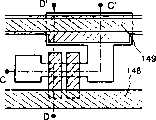
完成激活和氢化步骤之后,形成第二导体层用做栅极布线。这种第二导体层可以用导体层(D)和导体层(E)形成,导体层(D)主要由作为低电阻材料的铝(Al)或铜(Cu)组成,导体层(E)由钛(Ti)、钽(Ta)、钨(W)、或钼(Mo)制成。在此实施例中,导体层(D)145是含0.1-2wt%钛(Ti)的铝(Al)膜,导体层(E)146是钛(Ti)膜。导体层(D)145可以形成为200-400nm(最好是250-350nm),导体层(E)146可以形成为50-200nm(最好是100-150nm)(图4A)。After completing the activation and hydrogenation steps, a second conductor layer is formed for gate wiring. Such a second conductor layer can be formed with a conductor layer (D) mainly composed of aluminum (Al) or copper (Cu) as a low-resistance material, and a conductor layer (E) composed of Titanium (Ti), tantalum (Ta), tungsten (W), or molybdenum (Mo). In this embodiment, the conductor layer (D) 145 is an aluminum (Al) film containing 0.1-2 wt% titanium (Ti), and the conductor layer (E) 146 is a titanium (Ti) film. The conductor layer (D) 145 can be formed to 200-400nm (preferably 250-350nm), and the conductor layer (E) 146 can be formed to 50-200nm (preferably 100-150nm) (FIG. 4A).
导体层(E)146和导体层(D)145进行腐蚀处理,形成连接栅电极的栅极布线,如此形成栅极布线147、148和电容器布线149。腐蚀处理首先通过采用SiCl4、Cl2和BCl3的混合气体的干法腐蚀法,从导体层(E)的表面经过导体层(D)到达一半的去除,然后采用磷酸基腐蚀溶液进行湿法腐蚀,去除导体层(D),这样可以在形成栅极布线的同时保持以基底层的选择加工。The conductive layer (E) 146 and the conductive layer (D) 145 are etched to form a gate wiring connected to the gate electrode, thereby forming
图6B和图7B是这种状态的顶视图,其中剖面A-A’和剖面C-C’对应于图4B中的A-A’和C-C’。剖面B-B’和剖面D-D’对应于图8B和图9B的B-B’和D-D’。在图6B和7B中,部分栅极布线147、148交叠,已与部分栅电极128、129、131电接触。这种状态清楚地显示在对应于剖面B-B’和D-D’的图8B和9B的剖面结构图,其中形成第一导体层的导体层(C)和形成第二导体层的导体层(D)电接触。Figures 6B and 7B are top views of this state, in which section A-A' and section C-C' correspond to A-A' and C-C' in Figure 4B. Section B-B' and section D-D' correspond to B-B' and D-D' of Fig. 8B and Fig. 9B. In FIGS. 6B and 7B , part of the
采用氧化硅膜或氮氧化硅膜,形成厚500-1500nm的第一层间绝缘膜150,之后形成接触孔到达每个岛状半导体层中形成的源区或漏区,形成源布线151-154和漏布线155-158。虽然这里没有示出,但是在此实施例中,电极具有三层层叠结构,是通过溅射连续形成的100nmTi膜、300nm的含Ti铝膜和150nm的Ti膜。A silicon oxide film or a silicon oxynitride film is used to form a first
接着,形成厚50-500nm(一般是100-300nm)的氮化硅膜、氧化硅膜或氮氧化硅膜,作为钝化膜159。在此状态的氢化处理对TFT性能提高有利。例如,可以在含3-100%氢的气氛中、300-450℃进行1-12小时的热处理,或者通过使用等离子体氢化法可以达到类似的效果。这里,在要形成用于象素电极和漏布线的连接的接触孔的位置,在钝化膜159中形成开口(图4C)。Next, a silicon nitride film, a silicon oxide film, or a silicon oxynitride film is formed as the
图6C和图7C展示了这种情况的顶视图,其中剖面A-A’和剖面C-C’对应于图4C中的A-A’和C-C’。剖面B-B’和剖面D-D’对应于图8C和图9C中的B-B’和D-D’。图6C和图7C没有展示第一层间绝缘膜,但是岛状半导体层104、105、107的源区和漏区(未示出)中的源区布线151、152、154和漏区布线155、156、158,借助形成在第一层间绝缘膜的接触孔来连接。Figures 6C and 7C show top views of this case, where section A-A' and section C-C' correspond to A-A' and C-C' in Figure 4C. Section B-B' and section D-D' correspond to B-B' and D-D' in Fig. 8C and Fig. 9C. 6C and FIG. 7C do not show the first interlayer insulating film, but the
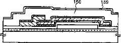
接着,形成厚1.0-1.5μm的有机树脂制成的第二层间绝缘膜160。所用的有机树脂可以是聚酰亚胺、丙稀酸、聚酰胺、聚酰亚胺氨化物、BCB(苯并环丁稀)等。这里,对衬底涂敷之后,采用热聚合型聚酰亚胺,在300℃烧结形成。然后在第二层间绝缘膜160中形成到达漏区布线158的接触孔,并形成象素电极161、162。使用的象素电极,在透射液晶显示器件的情形可以是透明导电膜,或者在反射液晶显示器件的情形可以金属膜。在此实施例中采用透射液晶显示器件,因此通过溅射形成厚100nm的氧化铟锡(ITO)膜(图5)。Next, a second interlayer insulating film 160 made of organic resin is formed to a thickness of 1.0-1.5 [mu]m. The organic resin used may be polyimide, acrylic acid, polyamide, polyimide amide, BCB (benzocyclobutene) and the like. Here, after the substrate is coated, thermally polymerized polyimide is used and sintered at 300°C. Then, a contact hole reaching the
按此方式制成在同一衬底上具有驱动电路TFT和显示区象素TFT的基片。在驱动电路上形成p-沟道TFT201、第一n-沟道TFT202和第二n-沟道TFT203,在显示区上形成象素TFT204和存储电容器205。在本说明书中,这种基片将简称为有源矩阵基片。In this way, a substrate having driver circuit TFTs and display area pixel TFTs on the same substrate is produced. A p-channel TFT 201, a first n-channel TFT 202 and a second n-channel TFT 203 are formed on the driving circuit, and a
驱动电路的p-沟道TFT201在岛状半导体层104中具有沟道形成区206、源区207a、207b和漏区208a、208b。第一n-沟道TFT202在岛状半导体层105中具有沟道形成区209、与栅电极129交叠LDD区210(以下这种LDD区将称为Lov)、源区211和漏区212。这种Lov区在沟道长度方向的长度是0.5-3.0μm,是1.0-1.5μm更好。第二n-沟道TFT203在岛状半导体层106中具有沟道形成区213、LDD区214、215、源区216和漏区217。这些LDD区由Lov区和不与栅电极130交叠的LDD区(以下这种LDD区将称为Loff)形成,这种Loff区在沟道长度方向的长度是0.3-2.0μm,是0.5-1.5μm更好。象素TFT204在岛状半导体层107中具有沟道形成区218、219、Loof区220-223、源区和漏区224-226。Loff区在沟道长度方向的长度是0.5-3.0μm,是1.5-2.5μm更好。电容器布线132、149和由与栅绝缘膜相同材料制成的绝缘膜连接于象素TFT204的漏区226,存储电容器205由添加n-型杂质元素的半导体层227形成。图5中象素TFT204具有双栅极结构,但是也可以是单栅极结构,采用具有多栅电极的多栅极结构没有问题。The p-channel TFT 201 of the driver circuit has a channel formation region 206 , source regions 207 a , 207 b , and drain regions 208 a , 208 b in the island-shaped
这样,本发明根据对象素TFT和驱动电路的技术要求,优化了每个电路的TFT结构,从而可改善半导体器件的工作性能和可靠性。此外,通过用耐热导电材料形成栅电极,可以有助于LDD区和源区和漏区的激活,从而通过用低电阻材料形成栅极布线来充分降低布线电阻。这样可以应用于在4英寸以上级别的显示区(屏幕尺寸)。In this way, the present invention optimizes the TFT structure of each circuit according to the technical requirements of the pixel TFT and the driving circuit, thereby improving the working performance and reliability of the semiconductor device. In addition, by forming the gate electrode with a heat-resistant conductive material, it is possible to facilitate activation of the LDD region and the source and drain regions, thereby sufficiently reducing wiring resistance by forming the gate wiring with a low-resistance material. This can be applied to display areas (screen sizes) on the order of 4 inches or more.
[实施模式2][Implementation Mode 2]
图16A-16C展示了栅电极和栅极布线的另一个实施例。按与实施模式1所示步骤相同的方式形成图16中的栅电极和栅极布线,形成在岛状半导体层901和栅绝缘膜902上16A-16C show another embodiment of the gate electrode and gate wiring. Form the gate electrode and gate wiring in FIG.
图16A中,作为栅电极的第一导体层,是由氮化钽(TaN)、氮化钨(WN)、氮化钛(TiN)或氮化钼(MoN)形成的导体层(A)903。导体层(B)904由选自钽(Ta)、钛(Ti)、钼(Mo)和钨(W)之中的元素,或者主要由这些元素组成的合金或包括这些元素组合的合金膜形成的,而导体层(C)905按与实施模式1相同的方式形成在表面上。导体层(A)903可以是10-50nm(最好是20-30nm),导体层(B)904可以是200-400nm(最好是250-350nm)。通过层叠导体层(D)906和位于其上的导体层(E)907形成作为栅极布线的第二导体层,导体层(D)906主要由作为低电阻材料的铝(Al)或铜(Cu)构成,导体层(E)907由钛(Ti)或钽(Ta)形成。由于通过应力迁移和电迁移而使铝(Al)和铜(Cu)快速扩散,所以氮化硅膜908必须形成为厚50-150nm,以便覆盖第二导体层。In FIG. 16A, the first conductor layer as the gate electrode is a conductor layer (A) 903 formed of tantalum nitride (TaN), tungsten nitride (WN), titanium nitride (TiN) or molybdenum nitride (MoN). . The conductor layer (B) 904 is formed of an element selected from tantalum (Ta), titanium (Ti), molybdenum (Mo), and tungsten (W), or an alloy mainly composed of these elements or an alloy film including a combination of these elements , and the conductor layer (C) 905 is formed on the surface in the same manner as in
图16B展示了按与实施模式1相同的方式制备的栅电极和栅极布线,掺杂了磷(P)的硅膜909形成在栅电极之下。掺杂了磷(P)的硅膜909具有防止栅电极中的微量碱金属元素扩散进入栅绝缘膜的作用,有利于保证TFT可靠性。FIG. 16B shows a gate electrode and a gate wiring prepared in the same manner as
图16C是在形成栅电极的第一导体层上形成掺杂磷(P)的硅膜910的例子。掺杂磷(P)的硅膜是电阻大于其它导体金属材料的材料,但是通过用铝(Al)或铜(Cu)形成由栅极布线构成的第二导体层,可以应用于大面积的液晶显示器件。这里,栅极布线可以是三层结构,通过达100nm的Ti膜911、达300nm的含Ti铝(Al)膜912和达150nm的Ti膜913来形成,避免铝(Al)膜和掺杂磷(P)的硅膜之间直接接触,提供耐热性。FIG. 16C is an example of forming a phosphorus (P)-doped
[实施模式3][Implementation Mode 3]
图15A-15C是根据本发明的TFT的结构示意图,展示了TFT中的栅电极和LDD区之间的位置关系,这种TFT具有半导体层沟道形成区、LDD区、位于半导体层上的栅极绝缘膜和位于栅极绝缘膜上的栅电极。15A-15C are schematic diagrams of the structure of a TFT according to the present invention, showing the positional relationship between the gate electrode and the LDD region in the TFT. This TFT has a semiconductor layer channel formation region, an LDD region, and a gate electrode located on the semiconductor layer. electrode insulating film and a gate electrode on the gate insulating film.
图15A展示的结构设置了具有沟道形成区209、LDD区210和漏区212的半导体层,和形成于其上的栅极绝缘膜120和栅电极129。LDD区210是通过栅极绝缘膜120与栅电极129交叠设置的Lov。Lov具有衰减靠近漏区产生的强电场的功能,同时防止热载流子引起的退化,能够适用于包括移位寄存器电路、电平漂移电路、缓冲电路等的驱动电路的n-沟道TFT。The structure shown in FIG. 15A provides a semiconductor layer having a channel formation region 209, an LDD region 210, and a drain region 212, and a
图15B展示的结构设置了具有沟道形成区213、LDD区215a、215b和漏区217的半导体层,和形成于半导体层上的栅极绝缘膜120和栅电极130。LDD区215a设置成通过栅极绝缘膜120与栅电极130交叠。而且,LDD区215b是不与栅电极130交叠设置的Loff。Loff具有降低截止电流值的功能,设置有Lov和Loff的结构能够防止热载流子引起的退化,同时还能够降低截止电流值,从而可以适用于驱动电路的取样电路的n-沟道TFT。The structure shown in FIG. 15B provides a semiconductor layer having a channel formation region 213,
图15C展示了设置有沟道形成区219、LDD区223和漏区226的半导体层。LDD区223是不通过栅极绝缘膜120与栅电极131交叠设置的Loff,其可以有效地降低截止电流值,因此适合用于象素TFT。象素TFT的LDD区223中的n-型杂质浓度最好比驱动电路的LDD区210、215中的浓度小1/2-1/10。FIG. 15C shows a semiconductor layer provided with a channel formation region 219 , an LDD region 223 and a drain region 226 . The LDD region 223 is Loff which is not overlapped with the
[实施模式4][Implementation Mode 4]
在此实施例中,将说明从有源矩阵衬底制备有源矩阵型液晶显示器件的步骤。如图11所示,按实施模式1制备的如图5所示状态下,在有源矩阵衬底上形成对准膜601。对于大多数液晶显示器件,常常采用聚酰亚胺树脂作为对准膜。在相反侧上的对置衬底602上,形成光屏蔽膜603、透明导体膜604和对准膜605。形成对准膜之后进行摩擦处理,以便按一致的预置倾角使液晶分子取向。通过公知的单元接合步骤,经过封接材料或衬垫(未示出),把象素矩阵电路和与其上已经形成了CMOS电路的有源矩阵对置的衬底装配在一起。然后,在两个衬底之间注入液晶材料606,采用密封剂(未示出)完成全部封接。使用的液晶材料可以是任何公知的液晶材料。这就制成了如图11所示的有源矩阵型液晶显示器件。In this embodiment, the steps of manufacturing an active matrix type liquid crystal display device from an active matrix substrate will be described. As shown in FIG. 11 , an
以下将参考图12的透视图和图13的顶视图,说明这种有源矩阵型液晶显示器件。图12和13中所用的相同标号对应于图1-5和图11的剖面结构图。沿图13中的E-E’的剖面结构对应于图5中的象素矩阵电路的剖面图。Such an active matrix type liquid crystal display device will be described below with reference to the perspective view of FIG. 12 and the top view of FIG. 13 . The same reference numerals used in Figs. 12 and 13 correspond to Figs. 1-5 and the sectional structural view of Fig. 11 . The sectional structure along E-E' in Fig. 13 corresponds to the sectional view of the pixel matrix circuit in Fig. 5 .
图12中,有源矩阵衬底由形成在玻璃衬底101上的显示区306、扫描信号驱动电路304和图象信号驱动电路305构成。象素TFT204设置显示区,围绕其设置的驱动电路由CMOS电路构成。扫描信号驱动电路304和图象信号驱动电路305分别通过栅极布线148和源区布线154连接到象素TFT204。而且,FPC731连接于外I/O接线端734,并且通过输入布线302、303连接到每个驱动电路。In FIG. 12, the active matrix substrate is composed of a
图13的顶视图展示了显示区306的大约一个象素部分。栅极布线148借助栅极绝缘膜(未示出)与其之下的半导体层107交叉。半导体层上未示出的还有源区、漏区和作为n-区的Loff区。连接器163存在于源区布线154和源区224之间,连接器164存在于漏区布线158和漏区226之间,连接器165存在于漏区布线158和象素电极161之间。存储电容器205形成的区中,从象素TFT204的漏区226延伸的半导体层227借助栅电极膜与电容器布线132、149交叠。The top view of FIG. 13 shows approximately one pixel portion of the
上面用实施模式1的结构说明了本实施例的有源矩阵型液晶显示器件,但是也可以采用与实施模式2的结构的任意组合制备有源矩阵液晶显示器件。The active-matrix liquid crystal display device of this embodiment has been described above using the structure of
[实施模式5][Implementation Mode 5]
图10是液晶显示器件的I/O接线端、显示区和驱动电路的排列示意图。显示区306具有按矩阵形式交叉的m个栅极布线和n个源区布线。例如,当象素密度是VGA(视频图形阵列)时,形成480个栅极布线和640个源区布线,对于XGA(扩展图形阵列),形成768个栅极布线和1240个源区布线。在13英寸级别显示的情况,显示区的屏幕尺寸具有340mm的对角线长度,在18英寸级别显示的情况是460mm。为了实现这种液晶显示器件,必须形成低电阻材料的栅极布线,如实施模式1和实施模式2所示。FIG. 10 is a schematic diagram of the arrangement of the I/O terminals, the display area and the driving circuit of the liquid crystal display device. The
围绕显示区306设置扫描信号驱动电路304和图象信号驱动电路305。由于随着显示区屏幕尺寸的增大,这些驱动电路栅极布线的长度也必须较长,所以最好由低电阻材料形成,如实施模式1和实施模式2所示,以便实现大尺寸屏幕。Around the
根据本发明,从输入端301连接于每个驱动电路的输入布线302、303,可以由与栅极布线相同的材料形成,它们能够有助于低的布线电阻。According to the present invention, the
[实施模式6][Implementation Mode 6]
图14是实施模式1或实施模式2所示有源矩阵衬底的结构视图,用于直观式显示器件结构。此实施例的有源矩阵衬底具有图象信号驱动电路1001、扫描信号驱动电路(A)1007、扫描信号驱动电路(B)1011、预充电电路1012和显示区1006。在本说明书中,术语“驱动电路”将包括图象信号驱动电路1001和扫描信号驱动电路(A)1007。Fig. 14 is a structural view of an active matrix substrate shown in
图象信号驱动电路1001设置有移位寄存器电路1002、电平漂移电路1003、缓冲电路1004和取样电路1005。扫描信号驱动电路(A)1007设置有移位寄存器电路1008、电平漂移电路1009和缓冲电路1010。扫描信号驱动电路(B)1011也具有相同的结构。The image signal drive circuit 1001 is provided with a shift register circuit 1002 , a level shift circuit 1003 , a buffer circuit 1004 and a sampling circuit 1005 . The scan signal drive circuit (A) 1007 is provided with a
移位寄存器电路1002、1008具有5-16V的驱动电压(一般是10V),形成这种电路的CMOS电路的n-沟道TFT适合具有如图5中202所示的结构。电平漂移电路1003、1009和缓冲电路1004、1010具有高达14-16V的驱动电压,对于移位寄存器电路,包括图5中的n-沟道TFT的CMOS电路是适合的。在这些电路中,用多栅极结构形成栅电极有利于提高耐电压能力和改善电路可靠性。The
取样电路1005具有14-16V的驱动电压,但是由于必须降低截止电流值,同时用交替反向的极性进行驱动,所以含有图5的n-沟道TFT203的CMOS电路是适合的。图5仅展示了n-沟道TFT,但是在实际取样电路中是与p-沟道TFT组合形成。这里,p-沟道TFT适合具有同一图中201所示的结构。The sampling circuit 1005 has a driving voltage of 14-16V, but since it is necessary to reduce the cut-off current value while driving with alternately reversed polarity, a CMOS circuit including the n-channel TFT 203 of FIG. 5 is suitable. Fig. 5 shows only n-channel TFT, but it is formed in combination with p-channel TFT in the actual sampling circuit. Here, the p-channel TFT suitably has the structure shown at 201 in the same figure.
象素TFT204具有14-16V的驱动电压,从降低功耗的来看,要求截止电流值比取样电路更为降低,因此该结构具有的LDD(Loff)区最好没有按象素TFT204那样方式与栅电极交叠。The pixel TFT204 has a driving voltage of 14-16V. From the perspective of reducing power consumption, the cut-off current value is required to be lower than that of the sampling circuit. Therefore, the LDD (Loff ) region of this structure is preferably not in the same way as the pixel TFT204. overlaps the gate electrode.
根据实施模式1所示的步骤制备TFT可以容易地实现此实施例的结构。在此实施例中,仅展示了用于显示区和驱动电路的结构,但是在实施模式1的步骤之后,可以在同一衬底上形成信号处理电路,例如信号分割电路、分谐波电路、D/A转换器、γ-校正电路、运算放大器电路、存储器电路或计算处理电路,或逻辑电路。这样,本发明能够在同一衬底上实现包括象素矩阵电路及其驱动电路的半导体器件,例如装配信号驱动电路和象素矩阵电路的半导体器件。The structure of this embodiment can be easily realized by preparing a TFT according to the steps shown in
[实施模式7][implementation mode 7]
根据本发明制备的有源矩阵衬底和液晶显示器件可以用于各种光电器件。本发明也可以用于任何含有这种光电器件作为显示介质的电子设备。作为电子设备这里可以列举个人计算机,数字照相机,录象机,便携式信息终端(移动计算机,蜂窝电话,电子书籍等),导航系统等。这些之中的例子如图17A-17E所示。The active matrix substrate and liquid crystal display device prepared according to the present invention can be used in various optoelectronic devices. The present invention can also be used in any electronic equipment containing such optoelectronic devices as display media. As the electronic equipment here, personal computers, digital cameras, video recorders, portable information terminals (mobile computers, cellular phones, electronic books, etc.), navigation systems, and the like can be cited. Examples of these are shown in Figures 17A-17E.
图17A是个人计算机,其由设置有微处理器或存储器的主体2001、图象输入器件2002、显示器件2003和键盘2004构成。可以根据本发明形成显示器件2003或其他信号处理电路。17A is a personal computer, which is composed of a
图17B是录象机,由主体2101、显示器件2102、声音输入器件2103、操作开关2104、电池2105和图象接收器件2106构成。本发明可以用于显示器件2102或其他信号驱动电路。17B is a video recorder, which is composed of a
图17C是便携式数字终端,由主体2201、图象输入器件2202、图象接收器件2203、操作开关2204和显示器件2205构成。本发明可以用于显示器件2205或其他信号驱动电路。17C is a portable digital terminal composed of a main body 2201, an image input device 2202, an image receiving device 2203, an operation switch 2204 and a display device 2205. The present invention can be used in display device 2205 or other signal driving circuits.
图17D是用于记录了节目的记录介质(以下简称为记录介质)的播放器,由主体2401、显示器件2402、扬声器2403、记录介质2404和操作开关2405构成。使用的记录介质可以是DVD(数字通用盘)或压缩盘(CD),可以重放音乐节目和图象显示,以及通过互连网显示视频节目(或TV节目)的数据。本发明可以满意地用于显示器件2402或其他信号驱动电路。FIG. 17D is a player for a recording medium (hereinafter simply referred to as recording medium) on which a program is recorded. The recording medium used may be a DVD (Digital Versatile Disc) or a Compact Disc (CD), and music programs and image displays can be played back, and data of video programs (or TV programs) can be displayed through the Internet. The present invention may be satisfactorily used in display device 2402 or other signal driving circuits.
图17E是数字照相机,由主体2501、显示器件2502、取景器2503、操作开关2504和图象接收器(未示出)构成。本发明可以用于图象器件2502或其他信号驱动电路。Fig. 17E is a digital camera, which is composed of a main body 2501, a display device 2502, a viewfinder 2503, operation switches 2504 and an image receiver (not shown). The present invention can be applied to image device 2502 or other signal driving circuits.
这样,本发明的应用范围极宽,能够用于各种领域的电子设备。这些实施例的电子设备也可以采用实施模式1-6的组合来实现。Thus, the application range of the present invention is extremely wide, and it can be used for electronic devices in various fields. The electronic devices in these embodiments can also be implemented by using a combination of implementation modes 1-6.
[实施模式8][implementation mode 8]
在本实施模式中,将说明由类似于实施模式1的有源矩阵衬底,制造采用电致发光(EL)材料的自发发光式显示屏(以下称为EL显示器件)的例子。图18A展示了EL显示屏的顶视图。图18A中,参考标号10是衬底,11是象素段,12是源区侧驱动电路,13是栅电极侧驱动电路,每个驱动电路通过布线14-16到达FPC17,然后连接于外部器件。In this embodiment mode, an example in which a self-luminescence display panel (hereinafter referred to as an EL display device) using an electroluminescent (EL) material is manufactured from an active matrix substrate similar to
图18B展示了在图18A的线A-A’的剖面。这里对置板80至少位于象素段之上,最好在驱动电路和象素段上。对置板80被封接材料19粘附在有源矩阵衬底上,其上形成TFT和采用EL材料的自发发光层。填料(图中未示出)混合在封接材料19中,两个衬底被这种填料粘附在一起,具有大致均匀的间距。该器件的结构通过封接材料19外侧和FPC17周边上的密封剂81密封。密封剂81使用例如硅树脂、环氧树脂、酚树脂或丁基橡胶等材料。Fig. 18B shows a cross section on line A-A' of Fig. 18A. Here the opposing
当有源矩阵衬底10和对置衬底80被封接材料19粘附在一起时,其内形成空隙。用填料83填充该空隙,这种填料83还具有粘附对置板80的作用。PVC(聚氯乙烯)、环氧树脂、硅树脂、PVB(聚乙烯醇缩丁醛)或EVA(乙烯乙酸乙烯酯)可以用做填料83。由于自发发光层的抗湿性较弱,易于退化,最好在填料83内形成干燥剂例如氧化钡,以便能够保持水分吸收效应。而且器件的结构还有在自发发光层上由氮化硅膜或氮氧化硅膜等形成钝化膜,以便防止包括填料83在内的碱性元素产生的腐蚀。When the
对置板80可以采用玻璃板、铝板、不锈钢板、FRP(玻璃纤维增强塑料)板、PVF(聚氯乙烯)膜、Myler膜(I.E.du Pont de Nemours and Company的商标)、聚酯膜、丙稀酸膜或丙稀酸板。而且,通过使用具有几十μm铝箔与PVF膜或Myler膜TM的夹层结构的片可以提高抗湿性。按此方式,EL元件被密封并与外界气氛屏蔽开。As the opposing
在图18B中,驱动电路TFT22(注意组合n-沟道TFT和p-沟道TFT的CMOS电路如图所示),和用于象素段的TFT23(注意控制到达EL元件的电流的TFT如此图所示)形成在衬底10和基膜21上。特别是,在这些TFT中,n-沟道TFT设置有构如本实施例所示的LDD区,防止导通电流因热载流子效应而降低,以及性能因第V次漂移或偏置应力而退化。In FIG. 18B, the driver circuit TFT22 (note that the CMOS circuit combining n-channel TFT and p-channel TFT is shown in the figure), and TFT23 for the pixel segment (note that the TFT controlling the current to the EL element is so As shown in the figure) is formed on the
例如,图5所示的p-沟道TFT201和n-沟道TFT202可以用做驱动电路TFT22。虽然其取决于驱动电压,如果驱动电压是10V以上,则图5的第一n-沟道TFT204或具有相同结构的p-沟道TFT可以用做象素段TFT。虽然第一n-沟道TFT202构成为设置有在漏区侧上与栅电极交叠的LDD,但是当驱动电压小于10V时并不必须这样设置,因为几乎可以忽略因热载流子效应引起的TFT退化。For example, p-channel TFT 201 and n-channel TFT 202 shown in FIG. 5 can be used as
为了从在图1A-1D状态的有源矩阵衬底制备EL显示器件,包括树脂材料的层间绝缘膜(平坦膜)26形成在源区布线和漏区布线上,包括电连接于象素段TFT23的漏区的透明导体膜的象素电极27形成于其上。氧化铟和氧化锡和化合物(称为ITO)或者氧化铟和氧化锌的化合物可以用做透明导体膜。形成象素电极27之后,形成绝缘膜28,在象素电极27上形成开孔段。In order to prepare an EL display device from the active matrix substrate in the state of FIGS. 1A-1D , an interlayer insulating film (flat film) 26 comprising a resin material is formed on the source wiring and the drain wiring, including electrically connected to the pixel segment. The
接着,形成自发发光层29。自发发光层29可以是层叠结构或单层结构,其中公知的EL材料(空穴注入层、空穴传送层、发光层、电子传送层或电子注入层)可以自由组合。考虑如何构成时可以采用公知范畴的技术。而且,对于EL材料有小分子材料和聚酯材料。在采用小分子材料的情形使用蒸发方法,在采用聚酯材料的情形可以使用简单方法,例如旋涂法、印刷法或喷墨法等。Next, the spontaneous
可以通过采用阴罩掩模的蒸发法、喷墨法或投放器法形成自发发光层。按这些方式,通过形成每个象素能够发出不同波长的光发光层(发红光层、发绿光层和发蓝光层),可以实现彩色显示。可以采用其它任何方式,例如色彩变化层(CCM)与滤色器组合,发白光层与滤色器组合。不用说也可以采用发单色光的EL显示器件。The spontaneous light emitting layer can be formed by an evaporation method using a shadow mask, an inkjet method, or a dispenser method. In these ways, by forming light-emitting layers (red, green, and blue) capable of emitting light of different wavelengths for each pixel, color display can be realized. Any other way can be used, such as color change layer (CCM) combined with color filter, white light emitting layer combined with color filter. It goes without saying that an EL display device emitting monochromatic light may also be used.
形成自发发光层29之后,在顶部形成阴极30。最好尽可能地去除阴极30和自发发光层29之间界面存在的水分和氧。因此必须采取如下措施,例如通过连续膜淀积在真空中形成自发发光层29和阴极30,或者在惰性气氛中形成自发发光层29,然后在不暴露大气的条件下形成阴极30。可以采用多室系统(群工具系统)淀积设备按本实施例进行上述膜淀积。After forming the self-
注意采用LiF(氟化锂)膜和Al(铝)膜的层叠结构用于实施模式8的阴极30。特别是,通过蒸发1nm厚的LiF(氟化锂)膜形成在自发发光层29上,在其上部形成300nm厚的铝膜。不用说,可以使用MgAg电极、公知电极材料。阴极30在参考标号31表示的区域与布线16连接。布线16是电源线,以便为阴极30提供预定的电压,并通过各向异性导电膏材料32与FPC17连接。在FPC17上还形成树脂层80,这段的粘附性得以提高。Note that a laminated structure of a LiF (lithium fluoride) film and an Al (aluminum) film is employed for the
为了在参考标号31代表的区域电连接阴极30和布线16,必须在层间绝缘膜26和绝缘膜28中形成接触孔。可以在层间绝缘膜26的腐蚀期间(当形成象素电极接触孔时)和绝缘膜28的腐蚀期间(当形成自发发光层之前形成开口段时)形成接触孔。而且,在腐蚀绝缘膜28时可以在整个过程中的一次发射中对层间绝缘膜26进行腐蚀。在这种情况,接触孔可以具有良好的形状,只要层间绝缘膜26和绝缘膜28是相同树脂材料即可。In order to electrically connect the
布线16穿过封接材料19和衬底10之间的空间(只要用密封剂81封闭即可)与FPC17连接。注意这里的说明是针对布线16,但是其它布线14和15也可以按类似方式穿过封接材料18之下与FPC17电连接。The
象素段的更详细剖面结构如图19A和19B所示,顶视图如图20A所示,电路图如图20B所示。在图19A中,设置在衬底2401上的开关TFT2402,按与实施模式1的图5的象素TFT204相同的结构形成。成为2个TFT通过采用双栅电极结构串联的结构,通过在不与栅电极交叠而设置的偏置区中形成LDD可以降低截止电流值。虽然本实施例使用双栅电极结构,但是结构可以是三栅电极结构或者具有更多栅电极的多栅电极结构。A more detailed cross-sectional structure of the pixel segment is shown in Figures 19A and 19B, a top view is shown in Figure 20A, and a circuit diagram is shown in Figure 20B. In FIG. 19A, switching TFT 2402 provided on
而且,采用如图5所示的第一n-沟道TFT202形成电流控制TFT2403。这种TFT结构是这样的结构,其中与栅电极交叠的LDD仅设置在漏区侧,通过降低寄生电容和栅极与漏区之间的串联电阻,提高了电流驱动器容量。而且从其它观点来看,应用这种结构具有非常重要的意义。由于电流控制TFT是控制流过EL元件的电流量的元件,所以该元件流过大量电流时存在因加热而退化和因热载流子而退化的较大危险。通过设置部分与栅电极交叠的LDD,可以防止电流控制TFT的退化,提高工作可靠性。此时,开关TFT2402的漏区布线35通过布线36与电流控制TFT的栅电极37电连接。参考标号38代表的布线是栅极布线,与开关TFT2402的栅电极39a和39b电连接。Also, a
而且,虽然本实施例展示了用于电流TFT2403的单栅极结构,但也可以是串联连接多个TFT多栅极结构。而且,可以是多个TFT并联连接、在效果上分开沟道形成区的结构,其中可以高效地获得热发射。这种结构是针对因加热而退化的有效对策。Also, although this embodiment shows a single gate structure for the
如图20A所示,成为电流控制TFT2403的栅电极37的布线,通过在参考标号2404代表的区设置绝缘膜,与电流控制TFT2403的漏区布线40交叠。在参考标号2404代表的区形成电容器。此电容器2404的作用是保持施加于电流控制TFT2403栅电极的电压。漏区布线40连接于电流线(电源线)2501,对其总是施加恒定电压。As shown in FIG. 20A, the wiring to become the
在开关TFT2402和电流控制TFT2403上形成第一钝化膜41,在其上形成包括树脂绝缘膜的平坦化膜42。采用平坦化膜42使因TFT产生的平面差平坦化是非常重要的。之后形成的自发发光层是如此之薄,以致存在平面差有时会导致发光缺陷。因此需要在形成象素电极之前进行平坦化处理,以便在尽可能平坦的表面上形成自发发光层。A
43代表的是具有高反射率的导电膜制成的象素电极(EL元件的阴极),与电流控制TFT2403的漏区电连接。象素电极43的优选材料是低电阻导电膜,例如铝合金膜、铜合金膜和银合金膜,或者这些膜的层叠膜。不用说,可以使用这些膜与其它导电膜形成层叠结构。由绝缘膜(最好是树脂)制成的边坡44a和44b在其间形成沟槽(对应于象素),在沟槽中形成发光层44。虽然这里仅展示了一个象素,但是可以形成分别对应于R(红)、G(绿)和B(蓝)色的发光层。作为形成发光层的有机EL材料采用π共轭聚酯材料。代表性的聚酯材料包括聚对亚苯基亚乙烯基(PPV)、聚乙烯咔唑(PVK)、和聚氟基材料等。在各种形式的PPV基有机EL材料中,有用的材料例如公开在H.Shenk,H.Becker,O.Gelsen,E.Kluge,W.Kreuder,and H.Spreitzer,“Polymers for Light EmittingDiodes,”Euro Display,Proceedings,1999,pp.33-37,或公开在日本专利申请公开平10-92576。43 represents a pixel electrode (the cathode of the EL element) made of a conductive film with high reflectivity, which is electrically connected to the drain region of the
具体地,采用氰基聚亚苯基亚乙烯基用于发射红光的发光层,采用聚亚苯基亚乙烯基用于发射绿光的发光层,采用聚亚苯基亚乙烯基或聚烷基亚苯基用于发射蓝光的发光层。其适当的膜厚是30-150nm(最好是40-100nm)。而且,上述说明是可用做发光层的有机EL材料,但本发明并不限于此。通过自由组合发光层、电荷输送层和电荷注入层,可以形成自发发光层(用于发光和用于移动载流子发光的层)。代替在本实施例所示例子中用做发光层的聚酯材料,例如可以采用小分子有机EL材料。也可以使用无机材料例如碳化硅,用于电荷输送层和电荷注入层。公知材料可以用做这些元件EL材料和无机材料。Specifically, cyanopolyphenylene vinylene is used for the light-emitting layer emitting red light, polyphenylene vinylene is used for the light-emitting layer emitting green light, polyphenylene vinylene or polyalkane The base phenylene is used for the light-emitting layer that emits blue light. Its suitable film thickness is 30-150nm (preferably 40-100nm). Also, the above description is of an organic EL material that can be used as a light-emitting layer, but the present invention is not limited thereto. By freely combining a light emitting layer, a charge transport layer, and a charge injection layer, a spontaneous light emitting layer (a layer for light emission and a layer for mobile carrier light emission) can be formed. Instead of the polyester material used as the light-emitting layer in the example shown in this embodiment, for example, a small molecule organic EL material may be used. Inorganic materials such as silicon carbide can also be used for the charge transport layer and the charge injection layer. Known materials can be used as these element EL materials and inorganic materials.
本实施例中的自发发光层具有层叠结构,其中包括PEDOT(聚三苯)或者PAni(聚苯胺)的空穴注入层46层叠在发光层45上。在本实施例的情形,在发光层45产生的光发射向顶面(向上超出TFT),这要求阳极具有透光性。透明导电膜可以由氧化铟和氧化锡的化合物形成,或者由氧化铟和氧化锌的化合物形成,优选的材料是能够在尽可能低的温度下形成膜的材料,因为在形成耐热性低的发光层和空穴注入层之后形成透明导电膜。The spontaneous light emitting layer in this embodiment has a laminated structure in which a
通过形成阳极47从而制成自发发光元件2045。这里的自发发光元件2045是指由象素电极(阴极)43、发光层45、空穴注入层46和阳极47构成的电容器。如图20A所示,象素电极43几乎延伸在全部象素区域上,从而全部象素起自发发光元件的作用。因此发光效率非常高,所以图象显示明亮。The self-luminous element 2045 is produced by forming the
在此实施例中,在阳极47上还形成第二钝化膜48。优选的第二钝化膜48是氮化硅膜或氮氧化硅膜。此第二钝化膜的目的在于使自发发光元件与外界封闭,防止有机EL材料因氧化而退化,以及抑制有机EL材料放气。这样可以提高EL显示器件的可靠性。In this embodiment, a
如上所述,本实施例的EL显示屏包括象素段,象素段包括如图20A所示的结构的象素,具有足够低的截止电流值的开关TFT,和抵抗热载流子能力强的电流控制TFT。如此获得的是具有高可靠性并且图象显示优异的EL显示屏。As described above, the EL display panel of the present embodiment includes pixel segments including pixels having a structure as shown in FIG. The current controls the TFT. Thus obtained is an EL display panel having high reliability and excellent image display.
图19B展示了自发发光层转变的例子。采用与图5的p-沟道TFT相同结构形成电流控制TFT2601。制备方法可以优选实施模式1。此实施例中采用透明导电膜用做象素电极(阳极)50。具体地,采用由氧化铟和氧化锌的化合物制成的导电膜。不用说,由氧化铟和氧化锡的化合物制成的导电膜也可以采用。Figure 19B shows an example of the transition of the spontaneous light-emitting layer. A
形成绝缘膜制成的边坡51a和51b之后,通过施加溶液形成包括聚乙烯咔唑的发光层52。在其上形成包括乙酰丙酮钾(表示为acacK)的电子注入层53和由铝合金制成的阴极54。此时,阴极54还起钝化膜的作用。如此形成EL元件2602。在此实施例中,发光层52中产生的光被发射朝向形成了TFT的衬底,如图中箭头所示。在采用本实施例的结构的情形,最好由p-沟道TFT形成电流控制TFT。After forming the
本实施例所示的EL显示器件可以用做实施模式7的电子器件的显示段。The EL display device shown in this embodiment can be used as a display segment of an electronic device of Embodiment Mode 7.
[实施模式9][implementation mode 9]
本实施例展示在图21A-21C,这些例子中象素具有不同于图20B的电路图的结构。在此实施例中,参考标号2701代表开关TFT2702的源区布线,2703代表开关TFT2702的栅极布线,2704代表电流控制TFT,2705代表电容器,2706和2708代表电流供给线,2707代表EL元件。This embodiment is shown in Figs. 21A-21C, in which the pixels have a structure different from that of the circuit diagram of Fig. 20B. In this embodiment,
图21A展示了两个象素共用电流供给线2706的例子。换言之,此例的特征在于与电流供给线2706对称地形成两个象素。此时,电流供给线的数量可以减少,可以进一步提高象素段的确定性(definition)。Fig. 21A shows an example in which two pixels share the current supply line 2706. In other words, this example is characterized in that two pixels are formed symmetrically to the current supply line 2706 . In this case, the number of current supply lines can be reduced, and the definition of the pixel segment can be further improved.
图21B展示了电流供给线2708布置成与栅极布线2703平行的例子。虽然电流供给线如此布置,不与图21B中的栅极布线2703交叠,但是如果这些线形成在不同的层,则两条线可以通过绝缘膜彼此交叠。此时,电流供给线2708和栅极布线2703可以共用其占据的区域,进一步提高象素段的确定性。FIG. 21B shows an example in which the current supply line 2708 is arranged in parallel with the
图21C所示例子的特征在于,电流供给线2708的布置与图21B的结构类似,与栅极布线2703平行,而且两个象素对称于电流供给线2708形成。使电流供给线2708与栅极布线2703之一交叠,这样的布置也是有效的。此时,可以减少电流供给线的数量,进一步提高象素段的确定性。虽然设置电容器2705以便保持在图21A和21B的电流控制TFT2704的栅电极施加的电压,但也可以省略电容器2705。The feature of the example shown in FIG. 21C is that the current supply line 2708 is arranged in parallel to the
由于如图19A所示的本发明的n-沟道TFT用做电流控制TFT2704,所以其具有的LDD区设置成通过插入的栅极绝缘膜与栅电极交叠。一般称为寄生电容的栅极电容形成在此交叠区,本实施例的特征在于使用寄生电容代替电容器2705。由于此寄生电容的电容量因栅电极和LDD区的交叠面积而变化,所以包含在交叠区的LDD区的长度决定了其电容量。而且,同样可以省略图21A-21C的结构的电容器2705。Since the n-channel TFT of the present invention as shown in FIG. 19A is used as the
注意本实施模式所示EL显示器件的电路结构可以选自实施模式1所示TFT结构,形成图21A-21C所示电路。可以使用本实施例的EL显示屏作为实施模式7的电子器件的显示段。Note that the circuit structure of the EL display device shown in this embodiment mode can be selected from the TFT structure shown in
[实施例][Example]
[实施例1][Example 1]
如实施模式1所示,TFT的栅电极和栅极布线在岛状半导体层之外接触,不插入接触孔。对这种结构的栅电极和栅极布线的电阻的评价结果如表1和2所示。表1展示了形成栅电极和栅极布线的薄层电阻。As shown in
表1:用于栅极和栅极总线的金属的各种薄层电阻
表2展示了由接触链(接触数量100-200)的测量值而计算的每个接触段的接触电阻的结果,这是为了评价栅电极和栅极布线的接触电阻。每个接触段的面积设定为4μm×10μm或6μm×10μm。Table 2 shows the results of the contact resistance of each contact segment calculated from the measured values of the contact chain (contact number 100-200), which is to evaluate the contact resistance of the gate electrode and gate wiring. The area of each contact segment was set to be 4 μm × 10 μm or 6 μm × 10 μm.
表2;栅极金属和栅极总线之间的每个接触链的接触电阻
对于栅电极,制备两种膜,即TaN膜和Ta膜的层叠膜和W膜。用Al形成栅极布线。注意向Al添加1wt%的Nd。(以下表示为Al-Nd膜)。当栅电极和栅极布线的交叠面积假设为40μm2,则接触电阻对于TaN膜和Ta膜的层叠膜大约是200Ω,对于W膜大约是0.1Ω。For the gate electrode, two kinds of films, a laminated film of a TaN film and a Ta film and a W film, were prepared. Al is used to form the gate wiring. Note the addition of 1 wt% Nd to Al. (hereinafter referred to as Al-Nd film). When the overlapping area of the gate electrode and the gate wiring is assumed to be 40 µm2 , the contact resistance is about 200Ω for a laminated film of TaN film and Ta film, and about 0.1Ω for a W film.
图22展示了采用透射电镜(TEM)对栅电极交叠段的观察结果,栅电极是通过层叠TaN膜和Ta膜,和W膜形成的。图23是Ta膜和Al-Nd膜之间界面的放大图,通过能量分布X-射线光谱(EDX)检测图中表示为*1和*4的点的成分。结果,虽然在*1检测到Al,在*4检测到Ta,但是发现形成了包括氧化物的层,这是因为在*2检测到Al和氧,在*3检测到Ta和氧。假设原因是Ta膜表面在用于杂质元素激活的热处理工艺中被氧化,这是在形成作为栅电极的Ta膜之后进行的。再形成Al-Nd膜时,Ta膜表面的氧估计氧化了Al-Nd膜。这样提高的接触电阻是采用Ta时显著出现的结果。FIG. 22 shows the results of observation using a transmission electron microscope (TEM) on an overlapping section of a gate electrode formed by laminating a TaN film and a Ta film, and a W film. Fig. 23 is an enlarged view of the interface between the Ta film and the Al-Nd film, and the compositions of the points indicated as* 1 and* 4 in the figure were examined by energy distribution X-ray spectroscopy (EDX). As a result, although Al was detected at* 1 and Ta was detected at* 4, it was found that a layer including oxide was formed because Al and oxygen were detected at* 2 and Ta and oxygen were detected at* 3. The reason is assumed to be that the surface of the Ta film is oxidized in the heat treatment process for impurity element activation, which is performed after forming the Ta film as the gate electrode. When the Al-Nd film is formed again, the oxygen on the surface of the Ta film presumably oxidizes the Al-Nd film. Such increased contact resistance is a remarkable consequence of the use of Ta.
但是,通过模拟接触电阻对信号波形施加的影响进行测试,证实了对200Ω左右的接触电阻的影响并不很大。图26A和26B展示了因波形上沿和波形下沿的电阻引起的差异。用于计算的等效电路如图中插图所示。这里通过从1Ω到1MΩ改变对应于接触电阻的R2进行模拟,证实了大至约10kΩ的接触电阻也几乎不能发现其影响。However, a test by simulating the influence of the contact resistance on the signal waveform has confirmed that the influence on the contact resistance of about 200Ω is not very large. Figures 26A and 26B illustrate the difference due to the resistance of the top and bottom edges of the waveform. The equivalent circuit used for the calculation is shown in the inset of the figure. Here, simulations were performed by changing R2 corresponding to the contact resistance from 1Ω to 1MΩ, and it was confirmed that the influence of the contact resistance as large as about 10kΩ was hardly found.
而且,作为接触段的可靠性测试进行导电性测试,考察接触电阻的差异。制备具有40μm2的接触段面积和接触数量200的测试样品,在180℃的气氛中导通1小时的1mA的电流。虽然对上述两种栅电极材料检测了接触电阻的差异,但是几乎观察不到差异。Furthermore, a conductivity test was performed as a reliability test of the contact section, and a difference in contact resistance was examined. A test sample having a contact section area of 40 μm2 and a contact number of 200 was prepared, and a current of 1 mA was conducted for 1 hour in an atmosphere of 180° C. Although the difference in contact resistance was detected for the above two gate electrode materials, almost no difference was observed.
[实施例2][Example 2]
通过偏置热应力实验(以下称为BT实验)研究制备的TFT的可靠性。TFT的尺寸是沟道长度为8μm,沟道宽度是8μm。实验条件是+20V的栅电极电压和0V的栅电极电压施加于n-沟道TFT,并在150℃保持1小时。图24A和24B展示了分别针对n-沟道TFT和p-沟道TFT的结果,但是在两种情形下几乎观察不到因偏置应力的退化。The reliability of the prepared TFT was investigated by a bias thermal stress experiment (hereinafter referred to as BT experiment). The dimensions of the TFT are a channel length of 8 μm and a channel width of 8 μm. The experimental conditions were that a gate voltage of +20V and a gate voltage of 0V were applied to the n-channel TFT and kept at 150°C for 1 hour. Figures 24A and 24B show the results for n-channel TFT and p-channel TFT, respectively, but almost no degradation due to bias stress was observed in both cases.
[实施例3][Example 3]
评价因栅极布线材料的差异而产生的信号延迟的影响。图25A和25B展示了信号输入段和输出段之间的波形差异,其中25A展示了波形上沿,25B展示了波形下沿。输入段和输出段之间的距离是83mm。图25A和25B中,表示为J2的特性是针对由Ta膜和Ta膜的层叠形成的栅极布线,表示为J4的样品是用Al-Nd膜的栅极布线形成的样品。栅极布线的宽度是10μm。虽然前者样品对于上沿时间和下沿时间在输入段和输出段之间有大的差异,但是后者样品具有极小的差异。J2样品的延迟时间是J4样品的大约10倍,从表1所示薄层电阻清晰可见,可以认为布线材料的电阻影响延迟时间。Evaluate the influence of signal delay due to differences in gate wiring materials. 25A and 25B show the waveform difference between the signal input section and the output section, wherein 25A shows the waveform's upper edge, and 25B shows the waveform's lower edge. The distance between the input section and the output section is 83mm. In FIGS. 25A and 25B , the characteristic indicated by J2 is for a gate wiring formed of a Ta film and a stack of Ta films, and the sample indicated by J4 is a sample formed of a gate wiring of an Al-Nd film. The width of the gate wiring is 10 μm. While the former sample has a large difference between the input and output segments for rising and falling times, the latter sample has very little difference. The delay time of the J2 sample is about 10 times that of the J4 sample, which is clearly seen from the sheet resistance shown in Table 1, and it can be considered that the resistance of the wiring material affects the delay time.
表3 单位:nsec
从上述结果可见,在显示尺寸是4英寸以上的情形,必须用正如本发明的低电阻材料形成与栅电极连接的栅极布线。As can be seen from the above results, in the case where the display size is 4 inches or more, it is necessary to form the gate wiring connected to the gate electrode with a low-resistance material as in the present invention.
通过使用本发明,可以使TFT具有半导体器件的功能电路的技术要求所适用的性能,上述半导体器件(本例中具体是光电器件)在同一衬底上形成有多功能电路,这样可使工作特性和可靠性有很大的提高。特别是,通过使象素矩阵电路的n-沟道TFT的LDD区形成为具有n-浓度并仅作为Loff,可以急剧地减低截止电流值,这有利于减低象素矩阵电路的功耗。而且,通过使驱动电路的n-沟道TFT的LDD区形成为具有n-浓度并仅作为Lov,可以提高电流驱动容量,防止因热载流子而产生的退化,这样减低了导通电流值的减低退化。还可以改善具有这种光电器件作为其显示介质的半导体器件(本例中具体是电子设备)的工作性能和可靠性。By using the present invention, TFT can be made to have the performance applicable to the technical requirements of the functional circuit of the semiconductor device. The above-mentioned semiconductor device (in this example, specifically the optoelectronic device) is formed with a multifunctional circuit on the same substrate, so that the operating characteristics can be improved. and reliability have been greatly improved. In particular, by forming the LDD region of the n-channel TFT of the pixel matrix circuit to have n- density as only Loff , the off current value can be drastically reduced, which contributes to the reduction of the power consumption of the pixel matrix circuit. Also, by forming the LDD region of the n-channel TFT of the driving circuit to have n- concentration and only as Lov , the current driving capacity can be improved, and degradation due to hot carriers can be prevented, thus reducing the on-current The decrease in value degenerates. It is also possible to improve the operational performance and reliability of semiconductor devices (specifically, electronic equipment in this example) having such optoelectronic devices as their display media.
此外,通过用高度耐热、导电材料形成象素TFT和驱动电路TFT的栅电极,形成用低电阻材料例如铝(Al)连接栅电极的栅极布线,可以实现上述满意的TFT性能,使用这种TFT来实现4英寸以上的大尺寸显示器件。In addition, the above-mentioned satisfactory TFT performance can be achieved by forming the gate electrodes of the pixel TFT and the driver circuit TFT with a highly heat-resistant, conductive material, and forming a gate wiring connecting the gate electrodes with a low-resistance material such as aluminum (Al), using this A TFT to realize a large-size display device of more than 4 inches.
Claims (40)
Translated fromChineseApplications Claiming Priority (3)
| Application Number | Priority Date | Filing Date | Title |
|---|---|---|---|
| JP10464699 | 1999-04-12 | ||
| JP104646/1999 | 1999-04-12 | ||
| JP104646/99 | 1999-04-12 |
Related Parent Applications (1)
| Application Number | Title | Priority Date | Filing Date |
|---|---|---|---|
| CNB001188097ADivisionCN1197157C (en) | 1999-04-12 | 2000-04-12 | Semiconductor device and method for manufacturing the same |
Related Child Applications (1)
| Application Number | Title | Priority Date | Filing Date |
|---|---|---|---|
| CN2006100737812ADivisionCN1870293B (en) | 1999-04-12 | 2000-04-12 | Semiconductor device and manufacturing method thereof |
Publications (2)
| Publication Number | Publication Date |
|---|---|
| CN1655038Atrue CN1655038A (en) | 2005-08-17 |
| CN1655038B CN1655038B (en) | 2010-05-12 |
Family
ID=14386237
Family Applications (4)
| Application Number | Title | Priority Date | Filing Date |
|---|---|---|---|
| CNB001188097AExpired - Fee RelatedCN1197157C (en) | 1999-04-12 | 2000-04-12 | Semiconductor device and method for manufacturing the same |
| CN2006100737812AExpired - Fee RelatedCN1870293B (en) | 1999-04-12 | 2000-04-12 | Semiconductor device and manufacturing method thereof |
| CNB2006101030029AExpired - Fee RelatedCN100481506C (en) | 1999-04-12 | 2000-04-12 | Semiconductor device and method for fabricating the same |
| CN2005100081531AExpired - Fee RelatedCN1655038B (en) | 1999-04-12 | 2000-04-12 | Semiconductor device and method for manufacturing the same |
Family Applications Before (3)
| Application Number | Title | Priority Date | Filing Date |
|---|---|---|---|
| CNB001188097AExpired - Fee RelatedCN1197157C (en) | 1999-04-12 | 2000-04-12 | Semiconductor device and method for manufacturing the same |
| CN2006100737812AExpired - Fee RelatedCN1870293B (en) | 1999-04-12 | 2000-04-12 | Semiconductor device and manufacturing method thereof |
| CNB2006101030029AExpired - Fee RelatedCN100481506C (en) | 1999-04-12 | 2000-04-12 | Semiconductor device and method for fabricating the same |
Country Status (6)
| Country | Link |
|---|---|
| US (5) | US7456430B1 (en) |
| EP (4) | EP2256817A2 (en) |
| JP (8) | JP2010219549A (en) |
| KR (1) | KR100733892B1 (en) |
| CN (4) | CN1197157C (en) |
| TW (1) | TW444257B (en) |
Cited By (2)
| Publication number | Priority date | Publication date | Assignee | Title |
|---|---|---|---|---|
| CN100550411C (en)* | 2005-11-16 | 2009-10-14 | 佳能株式会社 | display screen |
| CN102194892A (en)* | 2005-08-23 | 2011-09-21 | 株式会社半导体能源研究所 | Transistor, and display device, electronic device, and semiconductor device using the same |
Families Citing this family (41)
| Publication number | Priority date | Publication date | Assignee | Title |
|---|---|---|---|---|
| US6576926B1 (en)* | 1999-02-23 | 2003-06-10 | Semiconductor Energy Laboratory Co., Ltd. | Semiconductor device and fabrication method thereof |
| US6531713B1 (en)* | 1999-03-19 | 2003-03-11 | Semiconductor Energy Laboratory Co., Ltd. | Electro-optical device and manufacturing method thereof |
| TW444257B (en) | 1999-04-12 | 2001-07-01 | Semiconductor Energy Lab | Semiconductor device and method for fabricating the same |
| EP1049167A3 (en) | 1999-04-30 | 2007-10-24 | Sel Semiconductor Energy Laboratory Co., Ltd. | Semiconductor device and manufacturing method thereof |
| JP4666723B2 (en) | 1999-07-06 | 2011-04-06 | 株式会社半導体エネルギー研究所 | Method for manufacturing semiconductor device |
| SG116443A1 (en) | 2001-03-27 | 2005-11-28 | Semiconductor Energy Lab | Wiring and method of manufacturing the same, and wiring board and method of manufacturing the same. |
| KR100507278B1 (en)* | 2001-05-31 | 2005-08-09 | 비오이 하이디스 테크놀로지 주식회사 | Method for manufacturing thin film transistor lcd |
| TWI338346B (en) | 2002-09-20 | 2011-03-01 | Semiconductor Energy Lab | Display device and manufacturing method thereof |
| KR100493030B1 (en)* | 2002-11-08 | 2005-06-07 | 삼성전자주식회사 | Actuator locking apparatus for hard disk drive |
| WO2004057920A1 (en)* | 2002-12-19 | 2004-07-08 | Semiconductor Energy Laboratory Co., Ltd. | Display unit and method of fabricating display unit |
| CN101819984B (en)* | 2003-01-24 | 2014-04-30 | 株式会社半导体能源研究所 | Electronic book |
| US7221095B2 (en) | 2003-06-16 | 2007-05-22 | Semiconductor Energy Laboratory Co., Ltd. | Light emitting device and method for fabricating light emitting device |
| US7161184B2 (en) | 2003-06-16 | 2007-01-09 | Semiconductor Energy Laboratory Co., Ltd. | Display device and method for manufacturing the same |
| US7224118B2 (en) | 2003-06-17 | 2007-05-29 | Semiconductor Energy Laboratory Co., Ltd. | Display device and electronic apparatus having a wiring connected to a counter electrode via an opening portion in an insulating layer that surrounds a pixel electrode |
| SG142140A1 (en) | 2003-06-27 | 2008-05-28 | Semiconductor Energy Lab | Display device and method of manufacturing thereof |
| CN101577231B (en) | 2005-11-15 | 2013-01-02 | 株式会社半导体能源研究所 | Semiconductor device and method of manufacturing the same |
| US8395746B2 (en)* | 2006-01-31 | 2013-03-12 | Semiconductor Energy Laboratory Co., Ltd. | Display device |
| JP4321557B2 (en)* | 2006-07-06 | 2009-08-26 | エプソンイメージングデバイス株式会社 | Electro-optical device, method of manufacturing electro-optical device, and electronic apparatus |
| JP4991634B2 (en)* | 2008-06-09 | 2012-08-01 | キヤノン株式会社 | Organic EL light emitting device |
| KR101652693B1 (en) | 2008-10-03 | 2016-09-01 | 가부시키가이샤 한도오따이 에네루기 켄큐쇼 | Display device |
| JP5577646B2 (en)* | 2009-01-09 | 2014-08-27 | セイコーエプソン株式会社 | Electrophoretic display device, electronic apparatus, and method of manufacturing electrophoretic display device |
| US8461582B2 (en) | 2009-03-05 | 2013-06-11 | Semiconductor Energy Laboratory Co., Ltd. | Semiconductor device and method for manufacturing the same |
| US20100224878A1 (en)* | 2009-03-05 | 2010-09-09 | Semiconductor Energy Laboratory Co., Ltd. | Semiconductor device |
| KR101802406B1 (en) | 2009-11-27 | 2017-11-28 | 가부시키가이샤 한도오따이 에네루기 켄큐쇼 | Semiconductor device and method for manufacturing the same |
| US8415677B2 (en)* | 2010-01-20 | 2013-04-09 | International Business Machines Corporation | Field-effect transistor device having a metal gate stack with an oxygen barrier layer |
| US8304840B2 (en)* | 2010-07-29 | 2012-11-06 | Taiwan Semiconductor Manufacturing Company, Ltd. | Spacer structures of a semiconductor device |
| WO2012042564A1 (en) | 2010-09-29 | 2012-04-05 | パナソニック株式会社 | Thin-film semiconductor device for display device, method for producing thin-film semiconductor device for display device, el display panel and el display device |
| WO2012042566A1 (en) | 2010-09-29 | 2012-04-05 | パナソニック株式会社 | Thin-film semiconductor device for display device, method for producing thin-film semiconductor device for display device, el display panel and el display device |
| US9508904B2 (en)* | 2011-01-31 | 2016-11-29 | Cree, Inc. | Structures and substrates for mounting optical elements and methods and devices for providing the same background |
| JP5626010B2 (en)* | 2011-02-25 | 2014-11-19 | 富士通株式会社 | Semiconductor device, manufacturing method thereof, and power supply device |
| TW201322341A (en)* | 2011-11-21 | 2013-06-01 | Ind Tech Res Inst | Semiconductor component and method of manufacturing the same |
| TWI491050B (en)* | 2011-11-25 | 2015-07-01 | Sony Corp | Transistors, displays and electronic devices |
| TWI651839B (en)* | 2013-02-27 | 2019-02-21 | 半導體能源研究所股份有限公司 | Semiconductor device, drive circuit and display device |
| KR102086422B1 (en) | 2013-03-28 | 2020-03-10 | 삼성디스플레이 주식회사 | Display panel and method thereof |
| US11211000B2 (en)* | 2016-08-30 | 2021-12-28 | Sony Semiconductor Solutions Corporation | Display device and electronic device with differently layered wirings for pixel transistors |
| CN107134474B (en)* | 2017-06-12 | 2020-07-24 | 武汉华星光电半导体显示技术有限公司 | Thin film transistor and method of making the same, and organic electroluminescence display |
| US11049887B2 (en) | 2017-11-10 | 2021-06-29 | Applied Materials, Inc. | Layer stack for display applications |
| US10692799B2 (en)* | 2018-06-01 | 2020-06-23 | Innolux Corporation | Semiconductor electronic device |
| KR102600041B1 (en) | 2018-06-07 | 2023-11-08 | 삼성디스플레이 주식회사 | Organic light emitting diode display device |
| CN109686861B (en)* | 2018-12-26 | 2020-12-11 | 上海晶合光电科技有限公司 | Ring sleeve type discrete control patterned organic electroluminescent device and preparation method thereof |
| JP2023144395A (en)* | 2022-03-28 | 2023-10-11 | セイコーエプソン株式会社 | Electro-optical device and electronic apparatus |
Family Cites Families (136)
| Publication number | Priority date | Publication date | Assignee | Title |
|---|---|---|---|---|
| US699543A (en)* | 1896-06-03 | 1902-05-06 | Electric Vehicle Company | Motor-vehicle. |
| US679749A (en)* | 1901-03-12 | 1901-08-06 | Louis J Hirt | Coke-oven. |
| US710910A (en)* | 1902-01-09 | 1902-10-07 | John H Wescott | Compound engine. |
| JP3437863B2 (en)* | 1993-01-18 | 2003-08-18 | 株式会社半導体エネルギー研究所 | Method for manufacturing MIS type semiconductor device |
| JPS5847461A (en) | 1981-09-16 | 1983-03-19 | Takeda Chem Ind Ltd | Granule of chemical seasoning having high specific volume and its preparation |
| JPH0613612Y2 (en) | 1983-07-20 | 1994-04-13 | ヤンマー農機株式会社 | Angle control device for work equipment |
| JPS6096921A (en) | 1983-10-31 | 1985-05-30 | Yamatake Honeywell Co Ltd | Overcurrent detection circuit of electronic switch |
| JPH0613605Y2 (en) | 1986-03-03 | 1994-04-13 | 大介 藤井 | Trimming machine |
| JPH0194664A (en)* | 1987-10-05 | 1989-04-13 | Nec Corp | Field-effect transistor |
| JPH0827465B2 (en)* | 1988-04-06 | 1996-03-21 | 株式会社日立製作所 | Plane display |
| JPH01281434A (en)* | 1988-05-09 | 1989-11-13 | Toshiba Corp | Electrode forming method for display device |
| JP2720470B2 (en)* | 1988-08-26 | 1998-03-04 | 富士通株式会社 | Method of manufacturing thin film transistor matrix |
| JPH06104433B2 (en) | 1988-11-04 | 1994-12-21 | 株式会社小糸製作所 | Cornering lamp system for vehicles |
| JPH07113726B2 (en)* | 1989-01-10 | 1995-12-06 | 富士通株式会社 | Method of manufacturing thin film transistor matrix |
| JPH065852Y2 (en) | 1989-02-10 | 1994-02-16 | 駿河精機株式会社 | Foam plastic volume reduction machine |
| GB8909011D0 (en) | 1989-04-20 | 1989-06-07 | Friend Richard H | Electroluminescent devices |
| US5245207A (en) | 1989-04-21 | 1993-09-14 | Nobuo Mikoshiba | Integrated circuit |
| US5153690A (en)* | 1989-10-18 | 1992-10-06 | Hitachi, Ltd. | Thin-film device |
| US5266825A (en)* | 1989-10-18 | 1993-11-30 | Hitachi, Ltd. | Thin-film device |
| DE69032893T2 (en)* | 1989-11-30 | 1999-07-22 | Kabushiki Kaisha Toshiba, Kawasaki, Kanagawa | Material for electrical conductors, electronic device using this and liquid crystal display |
| JP3024620B2 (en) | 1990-04-11 | 2000-03-21 | セイコーエプソン株式会社 | Liquid crystal panel manufacturing method |
| GB2243948B (en) | 1990-04-20 | 1994-06-08 | Nobuo Mikoshiba | Integrated circuit |
| JP2628928B2 (en) | 1990-05-22 | 1997-07-09 | 株式会社フロンテック | Thin film transistor array and method of manufacturing the same |
| US5402254B1 (en)* | 1990-10-17 | 1998-09-22 | Hitachi Ltd | Liquid crystal display device with tfts in which pixel electrodes are formed in the same plane as the gate electrodes with anodized oxide films before the deposition of silicon |
| US5343063A (en)* | 1990-12-18 | 1994-08-30 | Sundisk Corporation | Dense vertical programmable read only memory cell structure and processes for making them |
| JPH04364723A (en)* | 1991-06-12 | 1992-12-17 | Kawasaki Steel Corp | Semiconductor device and manufacture thereof |
| JPH07111334B2 (en) | 1991-07-15 | 1995-11-29 | 協同組合ブライト北九州 | Surface shape measuring device |
| JPH0613612A (en)* | 1991-12-03 | 1994-01-21 | Nec Corp | Thin-film transistor |
| JPH05326960A (en)* | 1992-05-20 | 1993-12-10 | Seiko Epson Corp | Solid-state device with thin-film transistor and manufacture thereof |
| JPH065852A (en)* | 1992-06-23 | 1994-01-14 | Oki Electric Ind Co Ltd | Mosfet and manufacture thereof |
| DE69326123T2 (en) | 1992-06-24 | 1999-12-23 | Seiko Epson Corp., Tokio/Tokyo | THIN FILM TRANSISTOR AND METHOD FOR PRODUCING A THIN FILM TRANSISTOR |
| JP3189399B2 (en) | 1992-06-26 | 2001-07-16 | ソニー株式会社 | Method for manufacturing semiconductor device |
| EP0582486A2 (en) | 1992-08-07 | 1994-02-09 | Sharp Kabushiki Kaisha | A thin film transistor pair and a process for fabricating the same |
| JP2859784B2 (en) | 1992-09-03 | 1999-02-24 | シャープ株式会社 | Active matrix substrate |
| US5576556A (en)* | 1993-08-20 | 1996-11-19 | Semiconductor Energy Laboratory Co., Ltd. | Thin film semiconductor device with gate metal oxide and sidewall spacer |
| US6624477B1 (en)* | 1992-10-09 | 2003-09-23 | Semiconductor Energy Laboratory Co., Ltd. | Semiconductor device and method for manufacturing the same |
| TW232751B (en)* | 1992-10-09 | 1994-10-21 | Semiconductor Energy Res Co Ltd | Semiconductor device and method for forming the same |
| JP3587537B2 (en)* | 1992-12-09 | 2004-11-10 | 株式会社半導体エネルギー研究所 | Semiconductor device |
| JP3204764B2 (en)* | 1992-12-28 | 2001-09-04 | 日立金属株式会社 | Rotary sheet cutting device and manufacturing method thereof |
| US5583067A (en)* | 1993-01-22 | 1996-12-10 | Intel Corporation | Inverse T-gate semiconductor device with self-aligned punchthrough stops and method of fabrication |
| JPH06260499A (en) | 1993-03-02 | 1994-09-16 | Casio Comput Co Ltd | Thin-film transistor and manufacture thereof |
| US6150692A (en)* | 1993-07-13 | 2000-11-21 | Sony Corporation | Thin film semiconductor device for active matrix panel |
| JP2789293B2 (en)* | 1993-07-14 | 1998-08-20 | 株式会社半導体エネルギー研究所 | Semiconductor device manufacturing method |
| US5594569A (en) | 1993-07-22 | 1997-01-14 | Semiconductor Energy Laboratory Co., Ltd. | Liquid-crystal electro-optical apparatus and method of manufacturing the same |
| JPH07111334A (en) | 1993-08-20 | 1995-04-25 | Semiconductor Energy Lab Co Ltd | Semiconductor device and manufacture thereof |
| TW297142B (en)* | 1993-09-20 | 1997-02-01 | Handotai Energy Kenkyusho Kk | |
| JP3212060B2 (en) | 1993-09-20 | 2001-09-25 | 株式会社半導体エネルギー研究所 | Semiconductor device and manufacturing method thereof |
| US5719065A (en)* | 1993-10-01 | 1998-02-17 | Semiconductor Energy Laboratory Co., Ltd. | Method for manufacturing semiconductor device with removable spacers |
| JP2821347B2 (en)* | 1993-10-12 | 1998-11-05 | 日本電気株式会社 | Current control type light emitting element array |
| JP3431033B2 (en) | 1993-10-29 | 2003-07-28 | 株式会社半導体エネルギー研究所 | Semiconductor fabrication method |
| US5923962A (en) | 1993-10-29 | 1999-07-13 | Semiconductor Energy Laboratory Co., Ltd. | Method for manufacturing a semiconductor device |
| TW264575B (en) | 1993-10-29 | 1995-12-01 | Handotai Energy Kenkyusho Kk | |
| WO1995016797A1 (en) | 1993-12-14 | 1995-06-22 | Kabushiki Kaisha Toshiba | Molybdenum-tungsten material for wiring, molybdenum-tungsten target for wiring, process for producing the same, and molybdenum-tungsten wiring thin film |
| JPH07263705A (en) | 1994-03-24 | 1995-10-13 | Sony Corp | Thin film transistor |
| DE19500380C2 (en)* | 1994-05-20 | 2001-05-17 | Mitsubishi Electric Corp | Active matrix liquid crystal display and manufacturing method therefor |
| JPH07318975A (en) | 1994-05-25 | 1995-12-08 | Sanyo Electric Co Ltd | Liquid crystal display device |
| JP3232343B2 (en)* | 1994-05-31 | 2001-11-26 | 日本電信電話株式会社 | Horizontal MOS field-effect transistor |
| JP3281756B2 (en) | 1994-05-31 | 2002-05-13 | 三洋電機株式会社 | Semiconductor device and liquid crystal panel using the same |
| US5834827A (en)* | 1994-06-15 | 1998-11-10 | Seiko Epson Corporation | Thin film semiconductor device, fabrication method thereof, electronic device and its fabrication method |
| JP3072000B2 (en)* | 1994-06-23 | 2000-07-31 | 株式会社半導体エネルギー研究所 | Method for manufacturing semiconductor device |
| JP2692590B2 (en)* | 1994-06-29 | 1997-12-17 | 日本電気株式会社 | Semiconductor device and manufacturing method thereof |
| KR960009013A (en) | 1994-08-18 | 1996-03-22 | 김광호 | Titanium nitride (TiN) gate electrode formation method |
| JPH0864838A (en) | 1994-08-26 | 1996-03-08 | Casio Comput Co Ltd | Thin film transistor |
| JP3488551B2 (en) | 1994-09-29 | 2004-01-19 | 株式会社東芝 | Electrode wiring material and electrode wiring board using the same |
| US5738948A (en) | 1994-09-29 | 1998-04-14 | Kabushiki Kaisha Toshiba | Electrode-wiring material and electrode-wiring substrate using the same |
| JPH08125193A (en) | 1994-10-20 | 1996-05-17 | Semiconductor Energy Lab Co Ltd | Semiconductor integrated circuit and manufacturing method thereof |
| JPH09509288A (en) | 1994-11-30 | 1997-09-16 | マイクロン テクノロジー インコーポレイテッド | Method for depositing tungsten nitride using silicon-containing source gas |
| US5550066A (en)* | 1994-12-14 | 1996-08-27 | Eastman Kodak Company | Method of fabricating a TFT-EL pixel |
| JPH08179362A (en) | 1994-12-22 | 1996-07-12 | Mitsubishi Electric Corp | Thin film transistor array substrate |
| JPH08274336A (en)* | 1995-03-30 | 1996-10-18 | Toshiba Corp | Polycrystalline semiconductor thin film transistor and manufacturing method thereof |
| KR960039434A (en) | 1995-04-21 | 1996-11-25 | 김광호 | Transistor having metal gate electrode and manufacturing method thereof |
| JP3501874B2 (en) | 1995-05-24 | 2004-03-02 | 株式会社半導体エネルギー研究所 | How to make metal wiring |
| JPH0926600A (en) | 1995-07-13 | 1997-01-28 | Sanyo Electric Co Ltd | Liquid crystal display device |
| JPH0945789A (en) | 1995-07-27 | 1997-02-14 | Hitachi Ltd | Semiconductor device and manufacturing method thereof |
| KR0156202B1 (en) | 1995-08-22 | 1998-11-16 | 구자홍 | LCD and its manufacturing method |
| WO1997008752A1 (en) | 1995-08-25 | 1997-03-06 | Hitachi, Ltd. | Mis semiconductor device |
| JP3369811B2 (en) | 1995-09-13 | 2003-01-20 | 株式会社東芝 | Semiconductor device and method of manufacturing the same |
| JPH09153623A (en) | 1995-11-30 | 1997-06-10 | Sony Corp | Thin film semiconductor device |
| JP3239202B2 (en)* | 1995-12-01 | 2001-12-17 | シャープ株式会社 | MOS transistor and method of manufacturing the same |
| JP2865039B2 (en)* | 1995-12-26 | 1999-03-08 | 日本電気株式会社 | Method for manufacturing thin film transistor substrate |
| US5888858A (en)* | 1996-01-20 | 1999-03-30 | Semiconductor Energy Laboratory Co., Ltd. | Semiconductor device and fabrication method thereof |
| JPH09260629A (en)* | 1996-03-26 | 1997-10-03 | Sony Corp | Manufacture of amplified solid-state image pickup element |
| KR100193987B1 (en)* | 1996-05-11 | 1999-06-15 | 구자홍 | Driving circuit-integrated liquid crystal display device and manufacturing method |
| JPH09325358A (en)* | 1996-06-04 | 1997-12-16 | Sharp Corp | Liquid crystal display device and manufacturing method thereof |
| KR100207472B1 (en) | 1996-06-07 | 1999-07-15 | 윤종용 | Semiconductor device for gate electrode having & manufacturing method of the same |
| US5721163A (en)* | 1996-06-10 | 1998-02-24 | Chartered Semiconductor Manufacturing Pte, Ltd. | Method of manufacture of thin film transistor SRAM device with a titanium nitride or silicide gate |
| KR100209620B1 (en) | 1996-08-31 | 1999-07-15 | 구자홍 | Liquid crystal display device and its manufacturing method |
| EP0863495B1 (en)* | 1996-09-26 | 2005-08-24 | Seiko Epson Corporation | Display device |
| JP4032443B2 (en) | 1996-10-09 | 2008-01-16 | セイコーエプソン株式会社 | Thin film transistor, circuit, active matrix substrate, liquid crystal display device |
| JPH10135462A (en) | 1996-10-28 | 1998-05-22 | Matsushita Electric Ind Co Ltd | Thin film transistor |
| JP3457819B2 (en)* | 1996-11-28 | 2003-10-20 | カシオ計算機株式会社 | Display device |
| JP2988399B2 (en)* | 1996-11-28 | 1999-12-13 | 日本電気株式会社 | Active matrix substrate |
| JP3463971B2 (en)* | 1996-12-26 | 2003-11-05 | 出光興産株式会社 | Organic active EL light emitting device |
| JPH10319872A (en)* | 1997-01-17 | 1998-12-04 | Xerox Corp | Active matrix organic light emitting diode display |
| JP3864476B2 (en)* | 1997-01-24 | 2006-12-27 | ソニー株式会社 | Thin film semiconductor device |
| JPH10319909A (en)* | 1997-05-22 | 1998-12-04 | Casio Comput Co Ltd | Display device and driving method thereof |
| JPH10233505A (en) | 1997-02-21 | 1998-09-02 | Hitachi Ltd | Method for manufacturing semiconductor device |
| JPH10335334A (en)* | 1997-03-31 | 1998-12-18 | Seiko Epson Corp | Semiconductor device, method of manufacturing the same, and liquid crystal device |
| JP3346217B2 (en)* | 1997-04-04 | 2002-11-18 | カシオ計算機株式会社 | Wiring forming method and display device manufacturing method |
| JPH10319431A (en) | 1997-05-15 | 1998-12-04 | Advanced Display:Kk | Thin film transistor array substrate |
| JPH10326899A (en) | 1997-05-23 | 1998-12-08 | Semiconductor Energy Lab Co Ltd | Semiconductor device and its manufacture |
| JPH10325963A (en) | 1997-05-26 | 1998-12-08 | Sharp Corp | Method for manufacturing active matrix display device |
| JP3541625B2 (en)* | 1997-07-02 | 2004-07-14 | セイコーエプソン株式会社 | Display device and active matrix substrate |
| JP3830238B2 (en)* | 1997-08-29 | 2006-10-04 | セイコーエプソン株式会社 | Active matrix type device |
| JP4159633B2 (en) | 1997-09-19 | 2008-10-01 | 株式会社半導体エネルギー研究所 | Semiconductor device, manufacturing method thereof, and electronic apparatus |
| JPH1197707A (en) | 1997-09-24 | 1999-04-09 | Semiconductor Energy Lab Co Ltd | Method for manufacturing semiconductor device |
| US6218219B1 (en)* | 1997-09-29 | 2001-04-17 | Semiconductor Energy Laboratory Co., Ltd. | Semiconductor device and fabrication method thereof |
| JP3523093B2 (en) | 1997-11-28 | 2004-04-26 | 株式会社東芝 | Semiconductor device and manufacturing method thereof |
| JPH11194366A (en) | 1998-01-07 | 1999-07-21 | Seiko Epson Corp | Active matrix substrate and method of manufacturing the same, liquid crystal device and electronic equipment |
| JP4115586B2 (en)* | 1998-03-27 | 2008-07-09 | 株式会社半導体エネルギー研究所 | Method for manufacturing semiconductor device |
| US6482684B1 (en)* | 1998-03-27 | 2002-11-19 | Semiconductor Energy Laboratory Co., Ltd. | Method of manufacturing a TFT with Ge seeded amorphous Si layer |
| US6225168B1 (en)* | 1998-06-04 | 2001-05-01 | Advanced Micro Devices, Inc. | Semiconductor device having metal gate electrode and titanium or tantalum nitride gate dielectric barrier layer and process of fabrication thereof |
| JP2000082817A (en) | 1998-09-04 | 2000-03-21 | Sharp Corp | Active matrix substrate and manufacturing method thereof |
| JP2000111945A (en)* | 1998-10-01 | 2000-04-21 | Sony Corp | Electro-optical device, drive substrate for electro-optical device, and manufacturing method thereof |
| US6420758B1 (en)* | 1998-11-17 | 2002-07-16 | Semiconductor Energy Laboratory Co., Ltd. | Semiconductor device having an impurity region overlapping a gate electrode |
| WO2000031714A1 (en) | 1998-11-26 | 2000-06-02 | Seiko Epson Corporation | Electro-optical device and production method thereof and electronic equipment |
| US6420988B1 (en) | 1998-12-03 | 2002-07-16 | Semiconductor Energy Laboratory Co., Ltd. | Digital analog converter and electronic device using the same |
| US6469317B1 (en)* | 1998-12-18 | 2002-10-22 | Semiconductor Energy Laboratory Co., Ltd. | Semiconductor device and method of fabricating the same |
| US6259138B1 (en)* | 1998-12-18 | 2001-07-10 | Semiconductor Energy Laboratory Co., Ltd. | Semiconductor device having multilayered gate electrode and impurity regions overlapping therewith |
| US7510841B2 (en)* | 1998-12-28 | 2009-03-31 | Illumina, Inc. | Methods of making and using composite arrays for the detection of a plurality of target analytes |
| US6593592B1 (en)* | 1999-01-29 | 2003-07-15 | Semiconductor Energy Laboratory Co., Ltd. | Semiconductor device having thin film transistors |
| US6777716B1 (en)* | 1999-02-12 | 2004-08-17 | Semiconductor Energy Laboratory Co., Ltd. | Semiconductor display device and method of manufacturing therefor |
| US6576926B1 (en)* | 1999-02-23 | 2003-06-10 | Semiconductor Energy Laboratory Co., Ltd. | Semiconductor device and fabrication method thereof |
| JP3399432B2 (en)* | 1999-02-26 | 2003-04-21 | セイコーエプソン株式会社 | Electro-optical device manufacturing method and electro-optical device |
| US6614083B1 (en)* | 1999-03-17 | 2003-09-02 | Semiconductor Energy Laboratory Co., Ltd. | Wiring material and a semiconductor device having wiring using the material, and the manufacturing method |
| US6531713B1 (en) | 1999-03-19 | 2003-03-11 | Semiconductor Energy Laboratory Co., Ltd. | Electro-optical device and manufacturing method thereof |
| TW469484B (en) | 1999-03-26 | 2001-12-21 | Semiconductor Energy Lab | A method for manufacturing an electrooptical device |
| US6399988B1 (en) | 1999-03-26 | 2002-06-04 | Semiconductor Energy Laboratory Co., Ltd. | Thin film transistor having lightly doped regions |
| TW444257B (en) | 1999-04-12 | 2001-07-01 | Semiconductor Energy Lab | Semiconductor device and method for fabricating the same |
| JP4536202B2 (en)* | 1999-04-12 | 2010-09-01 | 株式会社半導体エネルギー研究所 | Semiconductor device, manufacturing method thereof, and electronic apparatus |
| EP1049167A3 (en) | 1999-04-30 | 2007-10-24 | Sel Semiconductor Energy Laboratory Co., Ltd. | Semiconductor device and manufacturing method thereof |
| US6661096B1 (en) | 1999-06-29 | 2003-12-09 | Semiconductor Energy Laboratory Co., Ltd. | Wiring material semiconductor device provided with a wiring using the wiring material and method of manufacturing thereof |
| US6171910B1 (en) | 1999-07-21 | 2001-01-09 | Motorola Inc. | Method for forming a semiconductor device |
| JP2003527860A (en) | 2000-03-23 | 2003-09-24 | イミューソル インコーポレイテッド | BRCA-1 regulatory factors and methods of use |
| CN1123465C (en)* | 2000-04-18 | 2003-10-08 | 李博良 | Truck preventer for preventing tail collision accident |
| KR100846762B1 (en)* | 2001-09-11 | 2008-07-16 | 삼성전자주식회사 | Key switch on keyboard unit |
- 2000
- 2000-04-06TWTW089106332Apatent/TW444257B/ennot_activeIP Right Cessation
- 2000-04-07USUS09/544,801patent/US7456430B1/ennot_activeExpired - Fee Related
- 2000-04-08KRKR1020000018404Apatent/KR100733892B1/ennot_activeExpired - Fee Related
- 2000-04-11EPEP10009810Apatent/EP2256817A2/ennot_activeWithdrawn
- 2000-04-11EPEP00107789Apatent/EP1045451A3/ennot_activeWithdrawn
- 2000-04-11EPEP07002100Apatent/EP1786037A3/ennot_activeWithdrawn
- 2000-04-11EPEP07002101.9Apatent/EP1780589A3/ennot_activeWithdrawn
- 2000-04-12CNCNB001188097Apatent/CN1197157C/ennot_activeExpired - Fee Related
- 2000-04-12CNCN2006100737812Apatent/CN1870293B/ennot_activeExpired - Fee Related
- 2000-04-12CNCNB2006101030029Apatent/CN100481506C/ennot_activeExpired - Fee Related
- 2000-04-12CNCN2005100081531Apatent/CN1655038B/ennot_activeExpired - Fee Related
- 2006
- 2006-04-03USUS11/396,436patent/US8129721B2/ennot_activeExpired - Fee Related
- 2006-07-14USUS11/487,010patent/US7855380B2/ennot_activeExpired - Fee Related
- 2010
- 2010-05-20JPJP2010116256Apatent/JP2010219549A/ennot_activeWithdrawn
- 2010-07-19USUS12/839,113patent/US8071981B2/ennot_activeExpired - Fee Related
- 2011
- 2011-04-08JPJP2011085976Apatent/JP5433618B2/ennot_activeExpired - Lifetime
- 2012
- 2012-03-05USUS13/411,842patent/US8866143B2/ennot_activeExpired - Fee Related
- 2012-12-19JPJP2012276399Apatent/JP5674754B2/ennot_activeExpired - Lifetime
- 2013
- 2013-05-07JPJP2013097406Apatent/JP2013201441A/ennot_activeWithdrawn
- 2014
- 2014-09-01JPJP2014176904Apatent/JP6130339B2/ennot_activeExpired - Lifetime
- 2015
- 2015-10-28JPJP2015211686Apatent/JP6022016B2/ennot_activeExpired - Lifetime
- 2016
- 2016-09-30JPJP2016193261Apatent/JP2017016154A/ennot_activeWithdrawn
- 2018
- 2018-02-15JPJP2018024697Apatent/JP6563051B2/ennot_activeExpired - Lifetime
Cited By (2)
| Publication number | Priority date | Publication date | Assignee | Title |
|---|---|---|---|---|
| CN102194892A (en)* | 2005-08-23 | 2011-09-21 | 株式会社半导体能源研究所 | Transistor, and display device, electronic device, and semiconductor device using the same |
| CN100550411C (en)* | 2005-11-16 | 2009-10-14 | 佳能株式会社 | display screen |
Also Published As
Similar Documents
| Publication | Publication Date | Title |
|---|---|---|
| CN1655038A (en) | Semiconductor device and manufacturing method thereof | |
| US6399988B1 (en) | Thin film transistor having lightly doped regions | |
| CN1373384A (en) | Semiconductor device and manufacturing method thereof | |
| CN1577435A (en) | Light emitting device | |
| CN1577028A (en) | Display device | |
| CN1855515A (en) | Semiconductor device and manufacturing method thereof | |
| CN1591922A (en) | Electronics device, semiconductor deivce, and method for manufacturing the same | |
| JP4536202B2 (en) | Semiconductor device, manufacturing method thereof, and electronic apparatus | |
| JP2000349299A (en) | Semiconductor device and its manufacture | |
| JP2001053286A (en) | Semiconductor film and manufacturing method thereof | |
| JP4527070B2 (en) | Semiconductor device, manufacturing method thereof, and electronic apparatus | |
| JP4618842B2 (en) | Method for manufacturing semiconductor device | |
| JP4527069B2 (en) | Display device | |
| KR100775130B1 (en) | Semiconductor device | |
| KR100775129B1 (en) | Semiconductor device |
Legal Events
| Date | Code | Title | Description |
|---|---|---|---|
| C06 | Publication | ||
| PB01 | Publication | ||
| C10 | Entry into substantive examination | ||
| SE01 | Entry into force of request for substantive examination | ||
| C14 | Grant of patent or utility model | ||
| GR01 | Patent grant | ||
| CF01 | Termination of patent right due to non-payment of annual fee | ||
| CF01 | Termination of patent right due to non-payment of annual fee | Granted publication date:20100512 Termination date:20180412 |