CN1649334B - Apparatus and method for adjusting quadrature modulator, and communication apparatus - Google Patents
Apparatus and method for adjusting quadrature modulator, and communication apparatusDownload PDFInfo
- Publication number
- CN1649334B CN1649334BCN200510005320.7ACN200510005320ACN1649334BCN 1649334 BCN1649334 BCN 1649334BCN 200510005320 ACN200510005320 ACN 200510005320ACN 1649334 BCN1649334 BCN 1649334B
- Authority
- CN
- China
- Prior art keywords
- offset
- signal
- value
- carrier
- values
- Prior art date
- Legal status (The legal status is an assumption and is not a legal conclusion. Google has not performed a legal analysis and makes no representation as to the accuracy of the status listed.)
- Expired - Fee Related
Links
Images


Classifications
- H—ELECTRICITY
- H04—ELECTRIC COMMUNICATION TECHNIQUE
- H04L—TRANSMISSION OF DIGITAL INFORMATION, e.g. TELEGRAPHIC COMMUNICATION
- H04L27/00—Modulated-carrier systems
- H04L27/32—Carrier systems characterised by combinations of two or more of the types covered by groups H04L27/02, H04L27/10, H04L27/18 or H04L27/26
- H04L27/34—Amplitude- and phase-modulated carrier systems, e.g. quadrature-amplitude modulated carrier systems
- H04L27/36—Modulator circuits; Transmitter circuits
- H04L27/362—Modulation using more than one carrier, e.g. with quadrature carriers, separately amplitude modulated
- H04L27/364—Arrangements for overcoming imperfections in the modulator, e.g. quadrature error or unbalanced I and Q levels
- H—ELECTRICITY
- H03—ELECTRONIC CIRCUITRY
- H03C—MODULATION
- H03C3/00—Angle modulation
- H03C3/38—Angle modulation by converting amplitude modulation to angle modulation
- H03C3/40—Angle modulation by converting amplitude modulation to angle modulation using two signal paths the outputs of which have a predetermined phase difference and at least one output being amplitude-modulated
Landscapes
- Engineering & Computer Science (AREA)
- Computer Networks & Wireless Communication (AREA)
- Signal Processing (AREA)
- Digital Transmission Methods That Use Modulated Carrier Waves (AREA)
Abstract
Description
Translated fromChinese技术领域technical field
本发明涉及无线通信装置的调制器,特别是涉及发信电路的正交调制器的IQ偏移量调整电路及方法。The present invention relates to a modulator of a wireless communication device, in particular to an IQ offset adjustment circuit and method of an orthogonal modulator of a signaling circuit.
背景技术Background technique
在移动电话终端等无线通信装置中,广泛应用有:QPSK(正交移相键控)、π/4移位QPSK、8PSK、HPSK(混合移相键控)等所谓在调制载波的I-Q平面上映射通信信息的调制方式。所述移动电话终端等形成如下结构:在基带一侧的电路中生成I、Q信号,并以正交调制器进行调制从而做成无线信号。In wireless communication devices such as mobile phone terminals, it is widely used: QPSK (Quadrature Phase Shift Keying), π/4 shift QPSK, 8PSK, HPSK (Hybrid Phase Shift Keying) and so on. On the I-Q plane of the modulated carrier Map the modulation method of the communication information. The mobile phone terminal and the like are configured such that I and Q signals are generated in a circuit on the baseband side and modulated by a quadrature modulator to form a wireless signal.
然而,在从基带一侧的电路输出的I、Q信号中,或如果正交调制器一侧的I、Q输入电路中有直流成分残留,则在被调制的无线信号中,载波成分重叠,并且所谓原点偏移变大,从而具有调制精度恶化,或解调一侧的错误增加等问题。由于所述直流偏移成分与设备相关而具有偏差特性,因而不会为零。如果在正交调制器的IQ输入电路中有直流成分残留,则直流成分会重叠在IQ的输入内,产生被称为“载波泄漏(carrier leak)”的不必要的信号。如果载波泄漏信号与信号成分相比较大,则成为调制输出信号的原点偏移变大而产生调制精度(EVM:误差矢量幅度)的下降,或在解调一侧的解调误差增大的主要原因。如上所述,由于偏移成分与设备(例如包括正交调制器的半导体设备)相关而具有偏差特性,因而不会为零,但如果在设备等中将偏移允许值设得很小,则在设备等制造时的检查中会由于偏移不良而使得成品率降低。However, if there is a DC component remaining in the I, Q signal output from the circuit on the baseband side, or in the I, Q input circuit on the quadrature modulator side, the carrier component overlaps in the modulated radio signal, In addition, the so-called origin shift increases, which leads to problems such as deterioration of modulation accuracy and increase of errors on the demodulation side. The DC offset component will not be zero due to its device-dependent bias nature. If there is a DC component remaining in the IQ input circuit of the quadrature modulator, the DC component will be superimposed on the IQ input, generating an unnecessary signal called "carrier leak". If the carrier leakage signal is larger than the signal component, it becomes the main cause of the decrease of the modulation accuracy (EVM: error vector magnitude) due to the increase of the origin shift of the modulated output signal, or the increase of the demodulation error on the demodulation side. reason. As described above, since the offset component has an offset characteristic depending on the device (for example, a semiconductor device including a quadrature modulator), it will not be zero, but if the offset allowable value is set small in the device, etc., then In the inspection at the time of manufacture of equipment and the like, the yield is lowered due to misalignment.
因此,在制造无线通信装置时,需要检测残留偏移成分,并将其消除的步骤。这些处理被称为“IQ信号的偏移调整”(在本说明书中也称为“IQ偏移调整”),在使用正交调制器的移动电话终端的制造中,这是必需的处理(工序)。Therefore, when manufacturing a wireless communication device, it is necessary to detect and eliminate residual offset components. These processes are called "offset adjustment of IQ signals" (also referred to as "IQ offset adjustment" in this specification), and are necessary in the manufacture of mobile phone terminals using quadrature modulators (process ).
下面对以往的IQ偏移调整法的典型例子进行概述。IQ偏移调整用于检测IQ信号各自的残留偏移值,并在IQ信号上有意地添加直流偏移来对其进行消除。由于I信号与Q信号为二维信号,因而很难同时调整I信号与Q信号二者。因此,可以利用IQ的正交性对I信号与Q信号的每一侧进行调整,使其变为最佳偏移消除量。Typical examples of conventional IQ offset adjustment methods will be outlined below. The IQ offset adjustment is used to detect the respective residual offset values of the IQ signals and remove them by intentionally adding a DC offset on the IQ signals. Since the I signal and the Q signal are two-dimensional signals, it is difficult to adjust both the I signal and the Q signal at the same time. Therefore, the orthogonality of IQ can be used to adjust each side of the I signal and the Q signal so that it becomes the optimum amount of offset cancellation.
首先,将I侧的偏移量设为固定值,并使Q侧的偏移量变化,测量几次,从而找出载波泄漏变得最小的Q侧的偏移,来作为Q侧的最佳点。同样,在最佳点固定求得的Q侧的偏移量,再使I侧的偏移量变化,从而将载波泄漏变得最小的值作为I侧的最佳点。First, set the offset on the I side to a fixed value, and change the offset on the Q side, and measure several times to find the offset on the Q side where the carrier leakage becomes the smallest, as the optimal value on the Q side. point. Similarly, by fixing the calculated offset on the Q side at the optimum point and changing the offset on the I side, the value at which the carrier leakage is minimized is taken as the optimum point on the I side.
再次固定I侧,使Q侧变化,求出最佳点。Fix the I side again and change the Q side to find the optimum point.
通过重复以上处理直至IQ偏移值不变化为止这样的步骤,来进行IQ偏移量的调整。The adjustment of the IQ offset amount is performed by repeating the above process until the IQ offset value does not change.
然而,在这种调整方法中,由于是逐次地或者是凭经验地求解I、Q偏移量,因而需要进行多次测量、调整,从而一台终端(无线通信装置)的调整所花费的时间不稳定,很费时。However, in this adjustment method, since the I and Q offsets are calculated successively or empirically, multiple measurements and adjustments are required, so the time spent on the adjustment of one terminal (wireless communication device) Unstable and time consuming.
另外,在后述专利文献1中,公开了通过多次原点偏移量的测量来算术地计算出应校正的IQ偏移量的结构。但是,该方法不测量载波泄漏量,而是要直接测量原点偏移量,所以每次必须设定一个IQ的偏移对。In addition,
专利文献1:日本专利文献特开2000-124964号公报(第4-5页,图4)Patent Document 1: Japanese Patent Application Laid-Open No. 2000-124964 (pages 4-5, FIG. 4 )
如上所述,对于以往的IQ偏移调整来说,由于在IQ偏移量中具有每个被调整对象的设备的偏差,需要进行I信号与Q信号的二维调整,因而需要技术人员的技术和时间。As mentioned above, in the conventional IQ offset adjustment, since the IQ offset amount has a deviation for each device to be adjusted, two-dimensional adjustment of the I signal and the Q signal is required, and technical skills of technicians are required. and time.
此外,在确定应校正的IQ偏移量中通常使用如下调整方法:经过多次操作,再在IQ信号中加上直流偏移,从而减少那时的载波泄漏量,此时,需要重复多次IQ偏移设定与载波泄漏量的测量,很费时间。In addition, the following adjustment method is usually used in determining the IQ offset that should be corrected: After multiple operations, add a DC offset to the IQ signal to reduce the carrier leakage at that time. At this time, it needs to be repeated many times IQ offset setting and carrier leakage measurement are very time-consuming.
另外,根据上述专利文献1,虽然测量次数本身大幅度减小,但重复多次测量与设定并没有改变,从而在调整上需要时间。长时间的调整时间在移动电话终端等的批量生产中会降低生产率,从而很难降低制造成本。In addition, according to the above-mentioned
发明内容Contents of the invention
因此,本发明的目的在于提供一种格外缩短发信电路的正交调制器的IQ偏移的调整时间,并实现高精度化,以及降低测试成本的装置及方法以及计算机程序。Therefore, an object of the present invention is to provide an apparatus, method, and computer program that significantly shorten the adjustment time of the IQ offset of the quadrature modulator of the transmission circuit, realize high precision, and reduce test costs.
本发明的另一个目的在于提供一种扩大正交调制器设备的I、Q信号的偏移、和/或增益等偏差的极限,从而降低产品成本的装置及方法以及计算机程序。Another object of the present invention is to provide a device, method and computer program for increasing the deviation limit of I, Q signal offset and/or gain of the quadrature modulator device, thereby reducing product cost.
达成所述目的的本发明的一个方式中的方法,是一种通过计算机导出正交调制器的I信号与Q信号的偏移(分别称为“I偏移”、“Q偏移”)的最佳调整值的方法,其中所述正交调制器使用从基带部输出的同相信号(称为“I信号”)及正交信号(称为“Q信号”)正交调制载波并将其输出,所述方法包括:The method in one mode of the present invention to achieve the above object is a method of deriving the offsets of the I signal and the Q signal of the quadrature modulator (referred to as "I offset" and "Q offset" respectively) by a computer. A method of optimum adjustment value, wherein the quadrature modulator uses an in-phase signal (referred to as "I signal") and a quadrature signal (referred to as "Q signal") output from the baseband section to quadrature-modulate the carrier and convert it output, the method includes:
对应至少为三组的在以I、Q成分为X、Y坐标的二维坐标平面上选择的并互不相同的I偏移与Q偏移的设定值,输入所述正交调制器的输出的载波泄漏电平的测量值的步骤,其中所述正交调制器将从所述基带部输出的I、Q信号作为输入;和Corresponding to at least three groups of set values of I offset and Q offset selected on a two-dimensional coordinate plane with I and Q components as X and Y coordinates and mutually different, inputting the set values of the quadrature modulator the step of outputting the measured value of the carrier leakage level, wherein the quadrature modulator takes as input the I, Q signals output from the baseband section; and
从与所述I偏移及Q偏移设定值的三组相对应的载波泄漏电平的测量值,求出与各组相对应的载波抑制比,从而导出I及Q偏移的最佳调整值的步骤。From the measured values of the carrier leakage levels corresponding to the three groups of the I offset and Q offset setting values, the carrier suppression ratio corresponding to each group is obtained, thereby deriving the optimum values of the I and Q offsets. Steps to adjust the value.
在本发明的方法中,可以不直接测量信号输出电平,而从与所述I偏移及Q偏移设定值的所述三组相对应的载波泄漏电平的绝对值求出信号输出电平,从而求出与各组相对应的载波抑制比,由此导出I及Q偏移的最佳调整值。In the method of the present invention, the signal output level can not be directly measured, but the signal output can be obtained from the absolute value of the carrier leakage level corresponding to the three groups of the I offset and Q offset setting values Level, so as to obtain the carrier suppression ratio corresponding to each group, and thus derive the optimal adjustment value of I and Q offset.
在本发明的方法中,包括:从与所述三组相对应的载波泄漏电平的测量值求出相对应的载波抑制比,且从所述载波抑制比分别求出所述二维坐标平面上的、到所述I、Q偏移的最佳调整点的距离的步骤;和In the method of the present invention, it includes: obtaining the corresponding carrier suppression ratio from the measured values of the carrier leakage levels corresponding to the three groups, and obtaining the two-dimensional coordinate plane from the carrier suppression ratio respectively The step of the distance to the optimal adjustment point of the I, Q offset; and
在所述二维坐标平面上,求出一个分别以所述I、Q偏移的设定值为中心、并且以到所述最佳调整点的距离为半径的三个圆的交点,从而导出所述I、Q偏移的最佳值的步骤。On the two-dimensional coordinate plane, find the intersection of three circles whose centers are the set values of the I and Q offsets and whose radius is the distance to the optimal adjustment point, thereby deriving The step of the optimal value of the I, Q offset.
根据本发明的另一个方式中的方法,是使用计算机调整正交调制器的I、Q信号的偏移(称为“I偏移、Q偏移”)时的方法,其中所述正交调制器以从基带部输出的同相信号(I信号)及正交信号(Q信号)正交调制载波并输出,该方法包括如下步骤:The method according to another aspect of the present invention is a method when using a computer to adjust the offset (referred to as "I offset, Q offset") of the I and Q signals of the quadrature modulator, wherein the quadrature modulation The carrier is quadrature-modulated and output with the in-phase signal (I signal) and the quadrature signal (Q signal) output from the baseband section, and the method includes the following steps:
(a)所述计算机对所述基带部设定I偏移与Q偏移的设定值,使其对应各自不同的设定时刻,其中所述I偏移与Q偏移的设定值与以I信号、Q信号为X、Y坐标的二维坐标平面上的、相互不同的至少三组相对应;(a) The computer sets the set values of the I offset and the Q offset to the baseband unit so that they correspond to different setting times, wherein the set values of the I offset and the Q offset are the same as On the two-dimensional coordinate plane with I signal and Q signal as X and Y coordinates, at least three groups corresponding to each other are different;
(b)测量装置通过至少一次的测量,从与所述三组I、Q偏移的设定值分别对应的、来自所述正交调制器的输出信号中,获得与所述三组I、Q偏移的设定值分别对应的三个载波泄漏电平;(b) The measuring device obtains the three sets of I, Q offsets from the output signals from the quadrature modulator respectively corresponding to the setting values of the three sets of I, Q offsets by at least one measurement, Three carrier leakage levels corresponding to the set values of Q offset;
(c)所述计算机从由所述测量装置测出的与所述三组I、Q偏移的设定值分别对应的三个载波泄漏电平的测量值中,分别求出载波抑制比,从而求出I、Q偏移的最佳调整值。(c) the computer calculates the carrier suppression ratio from the measured values of the three carrier leakage levels respectively corresponding to the set values of the three groups of I and Q offsets measured by the measuring device, In order to obtain the best adjustment value of I, Q offset.
在本发明中,还可以包括如下步骤:In the present invention, the following steps can also be included:
(d)所述计算机在所述基带部设定导出后的I、Q偏移的最佳调整值;(d) The computer sets the optimal adjustment value of the derived I and Q offsets in the baseband section;
(e)当在所述基带部设定所述I、Q偏移的最佳调整值之后的载波泄漏值收敛于规定值时,所述计算机结束调整,而当没有收敛于所述规定值时,转到所述步骤(a)的处理,从而在所述基带部设定所述其他组的I偏移与Q偏移的设定值。(e) When the carrier leakage value after setting the optimal adjustment values of the I and Q offsets in the baseband unit converges to a predetermined value, the computer ends the adjustment, and when the carrier leakage value does not converge to the predetermined value , go to the processing of the step (a), so as to set the setting values of the I offset and Q offset of the other group in the baseband unit.
本发明的另一个方式中的方法,是使用计算机调整正交调制器的I、Q信号的增益的方法,其中所述正交调制器以从基带部输出的同相信号(I信号)及正交信号(Q信号)正交调制载波并输出,所述方法包括如下步骤:The method in another aspect of the present invention is a method of using a computer to adjust the gains of I and Q signals of a quadrature modulator, wherein the quadrature modulator uses the in-phase signal (I signal) output from the baseband unit and the quadrature The quadrature signal (Q signal) modulates the carrier wave quadrature and outputs, and the method includes the following steps:
(a)所述计算机对所述基带部设定至少一组I信号与Q信号的增益的设定值;(a) the computer sets at least one set of I signal and Q signal gain setting values for the baseband unit;
(b)使用测量装置通过所述设定后的增益从所述正交调制器的输出信号测量出信号输出电平与边带泄漏,其中所述正交调制器将从所述基带部输出的I信号与Q信号作为输入;(b) using a measuring device to measure the signal output level and sideband leakage from the output signal of the quadrature modulator through the set gain, wherein the quadrature modulator outputs the I signal and Q signal as input;
(c)所述计算机从由所述测量装置测出的信号输出电平与边带泄漏导出与所述增益相对应的镜频抑制比,并在以I、Q成分为X、Y坐标的二维坐标平面上,从所述镜频抑制比导出I、Q增益的最佳值。(c) The computer derives the image frequency suppression ratio corresponding to the gain from the signal output level and sideband leakage measured by the measuring device, and uses the I and Q components as X and Y coordinates On the dimensional coordinate plane, the optimal values of I and Q gains are derived from the image frequency rejection ratio.
在本发明的方法中,还可以包括如下步骤:In the method of the present invention, the following steps can also be included:
(d)所述计算机在所述基带部设定导出后的I、Q增益的最佳值;(d) the computer sets the optimal value of the derived I and Q gains in the baseband section;
(e)当在所述基带部设定所述I、Q增益的最佳值之后的镜频抑制电平值收敛于规定值时,所述计算机结束调整,而当没有收敛于所述规定值时,转到所述步骤(a)的处理,从而在所述基带部设定所述其他的I、Q增益设定值。(e) When the image suppression level value after setting the optimum values of the I and Q gains in the baseband part converges to a specified value, the computer ends the adjustment, and when the value does not converge to the specified value , turn to the processing of the step (a), so as to set the other I and Q gain setting values in the baseband unit.
本发明的另一个方式中的装置是用于调整通信装置的I、Q偏移的装置,其中所述通信装置具有输出同相信号(I信号)及正交信号(Q信号)的基带部和正交调制器,其中所述正交调制器包括:移相器,用于使载波的相位移位.90度;第一、第二混频器,用于分别输入来自所述基带部的I、Q信号,并分别乘以所述载波与所述移相器的输出;加法器,用于将所述第一、第二混频器的乘法结果相加并输出输出信号,所述装置配有测量单元和控制所述测量单元及所述通信装置的数据处理单元,其中,所述数据处理单元包括下述装置,即,对所述通信装置的所述基带部设定I偏移与Q偏移的设定值,使其对应各自不同的设定时刻的装置,其中所述I偏移与Q偏移的设定值与以I、Q成分为X、Y坐标的二维坐标平面上的、相互不同的至少三组相对应;所述测量单元通过一次的测量,从来自所述正交调制器的输出信号获得与所述三组偏移设定值相对应的载波泄漏电平,并且所述数据处理单元包括如下装置,即,输入由所述测量单元得到的三组载波泄漏电平的测量值,并求出三组载波抑制比,从而求出I、Q偏移的最佳调整值的装置。A device in another aspect of the present invention is a device for adjusting I and Q offsets of a communication device having a baseband unit that outputs an in-phase signal (I signal) and a quadrature signal (Q signal) and a A quadrature modulator, wherein the quadrature modulator includes: a phase shifter, used to shift the phase of the carrier wave by .90 degrees; first and second mixers, used to input the I from the baseband section respectively , Q signal, and multiply the carrier and the output of the phase shifter respectively; an adder is used to add the multiplication results of the first and second mixers and output an output signal, and the device is configured There is a measurement unit and a data processing unit controlling the measurement unit and the communication device, wherein the data processing unit includes means for setting an I offset and a Q offset to the baseband part of the communication device. The setting value of the offset, so that it corresponds to the device at different setting moments, wherein the setting value of the I offset and the Q offset are on the two-dimensional coordinate plane with the I and Q components as the X and Y coordinates Corresponding to at least three groups that are different from each other; the measurement unit obtains the carrier leakage level corresponding to the three groups of offset setting values from the output signal from the quadrature modulator through one measurement, And the data processing unit includes the following devices, that is, input the measured values of the three groups of carrier leakage levels obtained by the measurement unit, and obtain the three groups of carrier suppression ratios, thereby obtaining the best I, Q offset A device for adjusting values.
在本发明中,最好不对频率分析器进行扫频,而是将中心频率固定为载波泄漏频率,并在固定调谐模式下进行测量,从而通过一次测量获取与所述各偏移设定值相对应的多个载波泄漏电平,其中所述频率分析器作为以来自所述正交调制器的输出信号为输入的测量装置。In the present invention, it is preferable not to sweep the frequency analyzer, but to fix the center frequency as the carrier leakage frequency, and to perform the measurement in the fixed tuning mode, so as to obtain the frequency corresponding to each offset setting value by one measurement. A corresponding plurality of carrier leakage levels, wherein the frequency analyzer acts as a measurement device having as input the output signal from the quadrature modulator.
本发明其他另一个方式中的程序,使调整正交调制器的I信号与Q信号的偏移(分别称为“I偏移”与“Q偏移”)的计算机,执行如下处理,其中所述正交调制器使用从基带部输出的同相信号(称为“I信号”)及正交信号(称为“Q信号”)正交调制载波并输出,所述处理为:The program in another aspect of the present invention causes a computer that adjusts the offsets of the I signal and the Q signal of the quadrature modulator (referred to as "I offset" and "Q offset" respectively) to perform the following processing, wherein The quadrature modulator uses the in-phase signal (referred to as "I signal") and the quadrature signal (referred to as "Q signal") output from the baseband section to quadrature modulate the carrier and output it. The process is as follows:
在所述基带部设定至少三组在以I、Q成分为.X、Y坐标的二维坐标平面上选择的、互不相同的I偏移及Q偏移的设定值的处理;The process of setting at least three sets of setting values of I offset and Q offset that are different from each other on the two-dimensional coordinate plane with I and Q components as X and Y coordinates in the baseband section;
从测量装置读出测量值的处理,其中所述测量装置测量所述正交调制器的输出的载波泄漏电平,所述正交调制器将从设定了所述三组I偏移及Q偏移的设定值的所述基带部输出的I、Q信号作为输入;The process of reading out measured values from a measuring device that measures the carrier leakage level of the output of the quadrature modulator from which the three sets of I offset and Q The I and Q signals output by the baseband part of the set value of the offset are used as input;
从与所述I偏移及Q偏移设定值的三组相对应的载波泄漏电平的测量值求出分别对应的载波抑制比,并导出I及Q偏移的最佳调整值的处理。The process of obtaining respectively corresponding carrier suppression ratios from the measured values of the carrier leakage levels corresponding to the three sets of I offset and Q offset setting values, and deriving optimal adjustment values of I and Q offsets .
本发明其他另一方式中的通信装置为如下构成,其具有输出同相信号(I信号)及正交信号(Q信号)的基带部和正交调制器,其中所述正交调制器包括:移相器,用于使载波的相位移位90度;第一、第二混频器,用于分别输入来自所述基带部的I、Q信号,并分别乘以所述载波与所述移相器的输出;加法器,用于将所述第一、第二混频器的乘法结果相加并输出输出信号,并且所述通信装置具有使I偏移与Q偏移的设定值分别对应预定的设定时刻并对其进行存储的装置,其中所述I偏移与Q偏移的设定值作为对所述基带部设定的I、Q偏移,与以I、Q成分为X、Y坐标的二维坐标平面上的、互不相同的至少三组分别对应;当进行偏移调整时,从来自所述正交调制器的输出信号,通过与所述三组偏移设定值相对应的载波泄漏电平测量值求出三组载波抑制比,从而在所述基带部设定导出的I、Q偏移值,并且所述基带部通过设定的I、Q偏移值,校正所述正交调制器的I、Q输入的偏移。A communication device in another aspect of the present invention has a configuration including a baseband unit that outputs an in-phase signal (I signal) and a quadrature signal (Q signal), and a quadrature modulator, wherein the quadrature modulator includes: A phase shifter is used to shift the phase of the carrier by 90 degrees; the first and second mixers are used to respectively input the I and Q signals from the baseband part and multiply the carrier and the shifted signal respectively. The output of the phase device; the adder is used to add the multiplication results of the first and second mixers and output the output signal, and the communication device has the setting values of the I offset and the Q offset respectively A device corresponding to a predetermined setting time and storing it, wherein the set values of the I offset and Q offset are used as the I, Q offset set for the baseband unit, and the I, Q components are On the two-dimensional coordinate plane of X and Y coordinates, at least three groups that are different from each other correspond to each other; when performing offset adjustment, from the output signal from the quadrature modulator, through the three groups of offset settings The carrier leakage level measurement value corresponding to the fixed value obtains three groups of carrier suppression ratios, thereby setting the derived I and Q offset values in the baseband part, and the baseband part passes the set I and Q offset values value to correct the offset of the I, Q inputs of the quadrature modulator.
本发明的其他方式的通信装置为如下构成,其具有输出同相信号(I信号)及正交信号(Q信号)的基带部和正交调制器,其中所述正交调制器包括:移相器,用于使载波的相位移位90度;第一、第二混频器,用于分别输入来自所述基带部的I、Q信号,并分别乘以所述载波与所述移相器的输出;加法器,用于将所述第一、第二混频器的乘法结果相加并输出输出信号,并且所述通信装置具有存储作为对所述基带部设定的I、Q增益的I信号与Q信号的增益的至少一组设定值的装置;当进行增益调整时,通过镜频抑制比而导出的I、Q增益的最佳值被设定在所述基带部,其中所述镜频抑制比与与来自所述正交调制器的所述增益的设定值相对应,并且从对信号输出电平与边带泄漏电平的测量结果中得出;A communication device according to another aspect of the present invention has a baseband unit that outputs an in-phase signal (I signal) and a quadrature signal (Q signal), and a quadrature modulator, wherein the quadrature modulator includes: The device is used to shift the phase of the carrier by 90 degrees; the first and second mixers are used to respectively input the I and Q signals from the baseband part, and multiply the carrier and the phase shifter respectively The output of; adder, is used for adding the multiplication result of described first, second mixer and output output signal, and described communication device has the I that is stored as the I, Q gain of described baseband part setting A device for at least one set of setting values for the gain of the I signal and the Q signal; when performing gain adjustment, the optimal value of the I and Q gain derived by the image frequency rejection ratio is set in the baseband section, wherein the said image rejection ratio corresponds to a setting of said gain from said quadrature modulator and is derived from measurements of signal output level and sideband leakage level;
所述基带部通过设定的I、Q增益值,来校正所述正交调制器的I、Q输入的增益。The baseband part corrects the gains of the I and Q inputs of the quadrature modulator according to the set I and Q gain values.
发明的效果The effect of the invention
根据本发明,可以不依赖于移动电话终端等的初期状态或者使用的正交调制器的残余偏移量,而可靠地调整IQ偏移,并可以谋求移动电话终端等的调整作业的简化,从而提高生产率。According to the present invention, the IQ offset can be reliably adjusted regardless of the initial state of the mobile phone terminal or the residual offset of the quadrature modulator used, and the adjustment work of the mobile phone terminal can be simplified, thereby Improve productivity.
此外,根据本发明,可以增大构成正交调制器的设备的制造偏差的许可范围,使之适于批量生产,并可使用更为廉价的设备。In addition, according to the present invention, the allowable range of manufacturing variation of devices constituting the quadrature modulator can be increased, making it suitable for mass production, and cheaper devices can be used.
附图说明Description of drawings
图1是本发明的一个实施方式的结构示意图;Fig. 1 is a structural representation of an embodiment of the present invention;
图2是本发明的一个实施方式的偏移调整的处理步骤的示意图;FIG. 2 is a schematic diagram of the processing steps of offset adjustment according to an embodiment of the present invention;
图3是用于说明本发明一个实施例的图;Figure 3 is a diagram for illustrating an embodiment of the present invention;
图4是用于说明本发明一个实施例的图;Figure 4 is a diagram for illustrating an embodiment of the present invention;
图5是固定TXQ偏移值,并使TXI偏移值变化时的载波抑制值的理论计算值的示意图;Fig. 5 is a schematic diagram of the theoretical calculation value of the carrier suppression value when the TXQ offset value is fixed and the TXI offset value is changed;
图6是IQ偏移坐标平面中的载波抑制比的示意图;Fig. 6 is a schematic diagram of the carrier suppression ratio in the IQ offset coordinate plane;
图7是IQ偏移校正量平面上的最佳点的示意图;Fig. 7 is a schematic diagram of an optimal point on the IQ offset correction plane;
图8是用于说明在本发明的一个实施例中,通过三点载波泄漏电平的绝对值的测量,导出最佳IQ偏移值的图;Fig. 8 is used for explaining in one embodiment of the present invention, through the measurement of the absolute value of three-point carrier leakage level, derives the figure of optimal IQ offset value;
图9是用于说明本发明一个实施例中的频谱分析器中的零档测量画面的图;FIG. 9 is a diagram for explaining a zero-scale measurement screen in a spectrum analyzer in an embodiment of the present invention;
图10是本发明的一个实施例的通信终端与测量装置的系统结构示意图;FIG. 10 is a schematic diagram of the system structure of a communication terminal and a measurement device according to an embodiment of the present invention;
图11是用于说明在本发明的一个实施例中,对模拟基带部的IQ偏移及增益设定的图;FIG. 11 is a diagram illustrating IQ offset and gain settings of an analog baseband unit in one embodiment of the present invention;
图12是本发明的另一个实施方式的增益调整的处理步骤的示意图;Fig. 12 is a schematic diagram of the processing steps of gain adjustment according to another embodiment of the present invention;
图13(A)是固定TXQ增益,并使TXI增益变化时的边带泄漏抑制(镜频抑制比)的理论值的示意图,图13(B)是在将IS比恒定时的A与B作为X轴、Y轴的TXIQ增益平面上进行图示的图;Fig. 13(A) is a schematic diagram of the theoretical value of sideband leakage suppression (image frequency suppression ratio) when the TXQ gain is fixed and the TXI gain is changed, and Fig. 13(B) is A and B when the IS ratio is constant as A graph that is illustrated on the TXIQ gain plane of the X-axis and Y-axis;
图14是用于说明本发明的另一个实施例中的最佳增益的导出的图。Fig. 14 is a diagram for explaining derivation of optimum gain in another embodiment of the present invention.
具体实施方式Detailed ways
为了对本发明进行更详细的叙述,参照附图进行说明。In order to describe the present invention in more detail, it will be described with reference to the accompanying drawings.
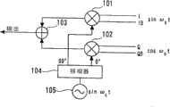
图1是本发明的一个实施方式的结构示意图。图1中示出了无线通信器的发信电路中的正交调制器(MOD)10和输出同相信号(I信号)与正交信号(Q信号)的模拟基带部(ABB)11之间的连接结构。发信电路的正交调制器10与模拟基带部11之间连接有作为IQ信号的TXI、TXIB和TXQ、TXQB(TXI、TXIB信号为差动信号,在I、Q端子上分别存在非反相信号I、Q和反相信号IB、QB)。另外,TXI、TXQ中的“TX”表示“发信”。Fig. 1 is a structural schematic diagram of an embodiment of the present invention. FIG. 1 shows the communication between the quadrature modulator (MOD) 10 and the analog baseband unit (ABB) 11 that outputs the in-phase signal (I signal) and quadrature signal (Q signal) in the transmission circuit of the wireless communicator. connection structure. TXI, TXIB and TXQ, TXQB (TXI, TXIB signals are differential signals as IQ signals are connected between the
正交调制器(MOD)10包括:混频器(乘法器)101、102;对混频器(乘法器)101、102的输出进行加法运算的加法器103;生成载波的本机振荡器105;将来自本机振荡器105的载波(正弦波)以及将其相位移位90度后的信号分别提供给混频器102、101的相位偏移器(移相器)104。混频器101差动输入来自模拟基带部11的互补的I成分TXI、TXIB,并与相位移位90度的载波进行乘法运算。混频器102差动输入互补的成分TXQ、TXQB,并与相位位移90度的载波进行乘法运算。来自本机振荡器105的载波也可以在差动模式下提供给混频器。混频器例如使用公知的吉尔伯特混频器等。在图1中,用正弦波表示载波,若用余弦波cos(ωct)表示载波,则载波和载波相位移位90度后的信号sin(ωct)被提供给混频器101、102。The quadrature modulator (MOD) 10 includes: mixers (multipliers) 101, 102; an
需要检测在作为IQ信号的输出侧的模拟基带部11和IQ输入侧的正交调制器10中分别产生的直流偏移成分,并消除IQ偏移量。图2是表示本发明的一个实施方式的IQ偏移调整的步骤的流程图。在本实施方式中,根据如图2所示的步骤,进行IQ偏移调整。It is necessary to detect DC offset components generated in each of the
在步骤S 1中,在模拟基带部11一侧多处设定IQ偏移。在模拟基带部11一侧装有用于每隔预先设定的一定时间间隔可变地设定TXIQ偏移、增益值的设定值的电路,从而输出反映了每隔设定时间的IQ偏移值的I、Q信号。In step S1, the IQ offset is set in multiple places on the
在接下来的步骤S2中,以测量装置来测量正交调制器的输出的载波泄漏量。即,最好通过频谱分析器的零档模式在一次测量中测出与按时间改变的IQ偏移值相对应的载波泄漏值。与每个预先设定时刻的IQ偏移值相对应的载波泄漏值的测量方法是本发明的特征之一,其具体内容将在后面叙述。In the next step S2, the carrier leakage amount of the output of the quadrature modulator is measured with a measuring device. That is, it is preferable to measure the carrier leakage value corresponding to the time-varying IQ offset value in one measurement by the zero-scale mode of the spectrum analyzer. The method of measuring the carrier leakage value corresponding to the IQ offset value at each preset time point is one of the characteristics of the present invention, and its specific content will be described later.
在接下来的步骤S3中,通过个人电脑等计算机计算出最佳偏移量。更详细地说,使用用于计算I、Q的直流偏移的规定的运算法则,从测得的载波泄漏值导出最佳IQ偏移量。最佳IQ偏移量的导出是本发明的特征之一,其具体内容将在后面叙述。In the next step S3, the optimum offset is calculated by a computer such as a personal computer. In more detail, the optimum IQ offset is derived from the measured carrier leakage value using a prescribed algorithm for calculating the I, Q DC offset. The derivation of the optimal IQ offset is one of the features of the present invention, and its specific content will be described later.
在接着的步骤S4中,在模拟基带部11中设定计算出的最佳I、Q偏移量。发信电路配有存储I、Q偏移量的存储电路,模拟基带部11的I、Q信号的输出电路基于设定的I、Q偏移量,使得DC偏移量可变。In the next step S4 , the calculated optimum I and Q offsets are set in the
在接着的步骤S5中,判断计算出的最佳I、Q偏移量中的载波泄漏量是否为规定值以下,当为规定值以下时结束调整,而当其比规定值大时,返回步骤S1。在步骤S1中,在模拟基带部11中设定其他组的I偏移与Q偏移的设定值。当判断出计算出的最佳I、Q偏移设定值中的载波泄漏量为规定值以下时,将该最佳I、Q偏移量的设定值存储保持在模拟基带部11中。此时,也可以将最佳I、Q偏移设定值记录到无线通信装置的EEPROM(可电擦除的读出专用存储器)等中。另外,在步骤S5中使用的规定值是可变化地自由设定的。In the following step S5, it is judged whether the carrier leakage amount in the calculated optimal I and Q offsets is below a predetermined value, and when it is below the predetermined value, the adjustment is terminated, and when it is greater than the predetermined value, return to the step S1. In step S1 , other set values of I offset and Q offset are set in the
根据本实施方式,基于以上的步骤,通常在一次测量中,高速地进行IQ偏移调整。According to the present embodiment, the IQ offset adjustment is usually performed at high speed in one measurement based on the above procedure.
另外,根据本实施方式,如后所述,获得自载波泄漏比至IQ调整目标之间的距离。下面进行说明。In addition, according to the present embodiment, the distance from the carrier-to-leakage ratio to the IQ adjustment target is obtained as described later. Described below.
参照如图3所示的正交调制器的结构,对本实施方式进行说明。在正交调制器的输入I-IB、Q-QB之间,产生正交调制器的输入残余偏移量与前段的模拟基带部的直流偏移的偏差量之和,并作为直流偏移成分加入到输入中,从而产生在IQ信号平面上的原点移位,成为导致EVM恶化的原因。因此,如上所述,需要通过将该偏移量原样逆加,以此需要消除直流偏移。This embodiment will be described with reference to the configuration of the quadrature modulator shown in FIG. 3 . Between the input I-IB and Q-QB of the quadrature modulator, the sum of the deviation of the input residual offset of the quadrature modulator and the DC offset of the analog baseband part of the previous stage is generated, and used as the DC offset component Added to the input, the origin shifts on the IQ signal plane, which becomes the cause of EVM deterioration. Therefore, as described above, it is necessary to cancel the DC offset by inverting the offset as it is.
下面,结合一个实施例对本发明进行详细说明。Below, the present invention will be described in detail in conjunction with an embodiment.
在图3所示的正交调制器中,若在I、Q信号中带有直流偏移(C,D),则输出Pout例如可以用下式(1)来表示。In the quadrature modulator shown in FIG. 3, if there is a DC offset (C, D) in the I and Q signals, the output Pout can be represented by the following formula (1), for example.
在上式(1)中,G为增益,k为正弦波的振幅,A为I信号的振幅,B为Q信号的振幅,C为I信号的直流偏移,D为Q信号的直流偏移。另外,增益G表示的是从图1的正交调制器的输入阶段至输出之间的增益。In the above formula (1), G is the gain, k is the amplitude of the sine wave, A is the amplitude of the I signal, B is the amplitude of the Q signal, C is the DC offset of the I signal, and D is the DC offset of the Q signal . In addition, the gain G represents the gain from the input stage to the output of the quadrature modulator in FIG. 1 .
图4是输出信号Pout的频率成分(频谱)的示意图。在图4中,频率ωb+ωc的频谱Output为期望的输出信号,在ωc与ωb-ωc的频率成分中分别产生了被称为“载波泄漏(carrier leak)”、“边带泄漏(side-band leak)”的不必要的信号成分(频谱)。从上式(1)可得知,这是由于在I、Q的输入中带有直流偏移,以及,I、Q信号的增益不平衡而产生的。FIG. 4 is a schematic diagram of the frequency components (spectrum) of the output signal Pout. In Fig. 4, the frequency spectrum Output of frequency ωb+ωc is the expected output signal, and the frequency components of ωc and ωb-ωc produce the so-called "carrier leak" and "side-band leakage" respectively. band leak)" unwanted signal components (spectrum). It can be known from the above formula (1) that this is caused by the DC offset in the I and Q inputs and the unbalanced gain of the I and Q signals.
根据上式(1),信号输出电平(Output level)、边带泄漏电平、载波泄漏电平可分别以下面的公式(2)、(3)、(4)求出。According to the above formula (1), the signal output level (Output level), sideband leakage level, and carrier leakage level can be obtained by the following formulas (2), (3), and (4) respectively.
载波泄漏电平相对于信号输出电平(Output level)的比、即载波抑制比(Carrier Suppression),以及,边带泄漏电平相对于信号输出电平(Output level)的比、即镜频抑制比(image suppression)分别以上式(3)、(4)与上式(2)的比来进行表示,从而以下面的公式(5)、(6)来表示。The ratio of the carrier leakage level to the signal output level (Output level), that is, the carrier suppression ratio (Carrier Suppression), and the ratio of the sideband leakage level to the signal output level (Output level), that is, the image frequency suppression The ratio (image suppression) is represented by the ratio of the above formulas (3), (4) and the above formula (2), respectively, and is expressed by the following formulas (5) and (6).
如果将IQ信号的振幅设为k[V],将I、Q的直流偏移设为TXIOffset[V]、TXQ Offset[V],则通过上式(5),将载波抑制比以下式(7)来表示。If the amplitude of the IQ signal is set to k[V], and the DC offsets of I and Q are set to TXIOffset[V] and TXQ Offset[V], then the carrier suppression ratio can be calculated by the following formula (7) through the above formula (5): )To represent.
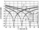
图5示出了将TXQ偏移值(TXQ Offset)固定后,使TXI偏移值(TXI Offset)变化时的载波抑制值的理论计算值。TXQ偏移值、TXI偏移值为0mV的点是没有额外的残余偏移、且载波抑制比最大的点。Fig. 5 shows the theoretical calculation value of the carrier suppression value when the TXI offset value (TXI Offset) is changed after the TXQ offset value (TXQ Offset) is fixed. The point where the TXQ offset value and TXI offset value are 0mV is the point where there is no additional residual offset and the carrier suppression ratio is the largest.
理论上,通过上式(7),在C2+D2=0时,载波抑制比成分为-∞(参照图5的TXI、TXQ=0mV的点)。Theoretically, according to the above formula (7), when C2 +D2 =0, the carrier suppression ratio becomes -∞ (refer to the point of TXI, TXQ=0mV in FIG. 5 ).
通过上式(7),
图5的图形相当于在图6的图形上,将TXQ偏移固定为恒定,而使TXI偏移变化时的图6的虚线的断面。The graph of FIG. 5 corresponds to the cross section of the dotted line in FIG. 6 when the TXQ offset is fixed and the TXI offset is changed on the graph of FIG. 6 .
由于在IQ偏移校正量平面内,载波抑制比以最佳调整点为中心,在同心圆上分布,因而如图6所示,根据载波抑制比的值,从现在的设定值到最佳调整点之间的距离r可以在下式(8)中求出。Because in the IQ offset correction plane, the carrier suppression ratio is distributed on concentric circles with the optimal adjustment point as the center, as shown in Figure 6, according to the value of the carrier suppression ratio, from the current set value to the optimal The distance r between the adjustment points can be obtained by the following equation (8).
若求解上式(5)的反函数,则r可在下式(9)中得出。另外,下式(9)中r的单位为[mV]。If the inverse function of the above formula (5) is solved, then r can be obtained in the following formula (9). In addition, the unit of r in the following formula (9) is [mV].
通过利用上式(9),测量载波抑制比,从而可以计算出到最佳调整点为止的、IQ偏移校正量平面上的距离。By measuring the carrier suppression ratio using the above formula (9), the distance on the IQ offset correction amount plane to the optimum adjustment point can be calculated.
接着,对本实施例中的信号电平的估算进行说明。通过上式(2),信号电平由G(增益)、k(正弦波的振幅值)、A、B(I、Q增益值)求出。由于k、A、B的值是预先设定的已知设定值,所以如果可以求出增益G的值,则可以求出信号输出电平。Next, the estimation of the signal level in this embodiment will be described. From the above formula (2), the signal level is obtained from G (gain), k (amplitude value of the sine wave), and A, B (I, Q gain values). Since the values of k, A, and B are known preset values, if the value of the gain G can be obtained, the signal output level can be obtained.
如图7所示,在IQ偏移校正量平面上,(e,f)为应求IQ偏移设定值的最佳点,载波抑制比以该最佳点(e,f)为中心,呈同心圆状分布。As shown in Figure 7, on the plane of the IQ offset correction amount, (e, f) is the optimal point for asking for the IQ offset setting value, and the carrier suppression ratio is centered on the optimal point (e, f), Distributed in concentric circles.
由于根据上式(4),信号输出电平为恒定值,所以可以说上式(3)的载波泄漏电平也是以最佳点为中心,呈同心圆状分布。图7的圆为同一载波泄漏电平。Since the signal output level is a constant value according to the above formula (4), it can be said that the carrier leakage level of the above formula (3) is also centered on the optimum point and distributed in concentric circles. The circles in Fig. 7 represent the same carrier leakage level.
在图7中,测量与IQ偏移校正量平面上的(a,b)、(a+d,b)、(a,b+d)三点相对应的载波泄漏电平。如果设此时的
这里,由于表示图7中的测量点与最佳点之间的距离,因而可以从三点各自的测量点与最佳点之间的距离及坐标,导出下式(11)所示的三个式子。为了简便,设rN=10(CL/20),并将r1作为(a,b)点上的值,r2作为(a+d,b)点上的值,r3作为(a,b+d)点上的值。Here, due to Represents the distance between the measurement point and the optimal point in FIG. 7, so the three formulas shown in the following formula (11) can be derived from the distances and coordinates between the respective measurement points and the optimal point of the three points. For simplicity, let rN=10(CL/20) , and take r1 as the value at (a, b), r2 as the value at (a+d, b), and r3 as (a, b+d) point value.
如果就a,b,d,r1,r2,r3求解上式(11)的G,则可导出下式(12)。When G of the above formula (11) is solved for a, b, d, r1, r2, r3, the following formula (12) can be derived.
即,变为G的四次方程式,由于G>0,因而增益G由下式(13)得出。That is, it becomes a quartic equation of G, and since G>0, the gain G is obtained by the following equation (13).
其中,in,
A=2d4A=2d4
通过将由上式(13)导出的G代入式(2),从而可以计算出信号输出电平(Output level)。By substituting G derived from the above formula (13) into formula (2), the signal output level (Output level) can be calculated.
由以上可知,根据本实施方式,不必直接测量信号输出电平,而能够仅从三点载波泄漏电平的绝对值计算出信号输出电平,并计算出载波抑制比。As can be seen from the above, according to this embodiment, it is not necessary to directly measure the signal output level, but the signal output level can be calculated only from the absolute value of the three-point carrier leakage level, and the carrier suppression ratio can be calculated.
从三点载波泄漏电平的绝对值求出三点载波抑制比,再从该载波抑制比求出到最佳调整点之间的距离。The three-point carrier suppression ratio is obtained from the absolute value of the three-point carrier leakage level, and then the distance to the optimal adjustment point is obtained from the carrier suppression ratio.
通过求得的到调整点的距离和测量点的IQ偏移校正平面上的座标,以测量点为中心,画出以到调整点的距离为半径的圆。在测量的三点上,分别画出该圆后,在几何上三个圆交于一点。该交点为应求偏移的最佳调整点。By obtaining the distance to the adjustment point and the coordinates on the IQ offset correction plane of the measurement point, with the measurement point as the center, draw a circle with the distance to the adjustment point as the radius. On the three measured points, draw the circle respectively, geometrically the three circles intersect at one point. The intersection point is the best adjustment point for the required offset.
接着,当测量与IQ偏移校正量平面上的(-m,-m)、(-m,m)、(m,-m)三点相对的载波泄漏电平时,成为如图8所示的情况,三点的圆的方程式被表示为下式(15)那样。Next, when the carrier leakage level relative to the three points (-m, -m), (-m, m), (m, -m) on the IQ offset correction plane is measured, it becomes as shown in Fig. 8 In this case, the equation of the three-point circle is expressed as the following equation (15).
解出上式(15)的方程式后,构成I、Q偏移的最佳设定值的目标收敛点(e,f)以下式(16)求出。After solving the equation of the above equation (15), the target convergence point (e, f) constituting the optimal setting value of the I, Q offset is obtained by the following equation (16).
由以上表示出,通过三点载波泄漏电平的绝对值的测量,能够检测出最佳IQ偏移值。It is shown from the above table that the best IQ offset value can be detected by measuring the absolute value of the three-point carrier leakage level.
然而,当测量三点载波泄漏电平的绝对值时,若通过一点一点地改变IQ偏移值来进行测量,则在IQ偏移值的设定、写入上需要时间。However, when measuring the absolute value of the three-point carrier leakage level, if the measurement is performed by changing the IQ offset value little by little, it takes time to set and write the IQ offset value.
因此,在本实施方式中,在硬件电路中具有可以每隔恒定时间就设定多个IQ偏移值的结构,从而一下求出三点的载波泄漏值,并在短时间内进行调整,由此,显著地缩短了调整时间。另外,使IQ偏移值变化的时间间隔(时刻的间隔)可以变化。Therefore, in the present embodiment, the hardware circuit has a configuration in which a plurality of IQ offset values can be set at regular intervals, thereby calculating the carrier leakage values of three points at once and adjusting them in a short time. Therefore, the adjustment time is significantly shortened. In addition, the time interval (time interval) at which the IQ offset value is changed may be changed.
在本实施例中,通过进行频谱分析器(外差方式)的零档模式下的测量(参照图9),从而可以在一次中测出与每隔恒定时间而设定的IQ偏移值相对应的载波泄漏值。即,根据本实施例,可通过由频谱分析器进行的一次测量来进行IQ的调整,从而实现IQ调整时间的缩短。In this embodiment, by performing measurement in the zero-scale mode of the spectrum analyzer (heterodyne method) (see FIG. 9 ), it is possible to measure the IQ offset value corresponding to the IQ offset value set every constant time at one time. Corresponding carrier leakage value. That is, according to the present embodiment, IQ adjustment can be performed by one measurement by the spectrum analyzer, thereby shortening the IQ adjustment time.
在本实施例中,有如下构成:由于在图1的模拟基带部11的输出与正交调制器10的输入上产生的制造偏差而产生的直流IQ偏移值,使用在模拟基带部11中设定的IQ偏移值来消除,此外,IQ振幅值以IQ增益值来进行调整。In this embodiment, there is the following configuration: the DC IQ offset value produced due to the manufacturing deviation between the output of the
图10是本发明的一个实施例的测量系统的结构示意图。参照图10,作为被测装置的移动电话终端机等终端1包括:正交调制器10、包括放大器12的无线(RF)部13、天线14、模拟基带部(ABB)11、数字基带部(DBB)15、终端1内的控制计算机(CCPU)17、存储器16、I/O端口19,并且还包括:在测量时将放大器12的输出切换到I/O端口19的输出端子上的切换开关18。数字基带部(DBB)15将串联数据系列转换成并联数据,并生成与一组并联数据相对应的基带信号,且在实验时,生成预定的实验信号(例如正弦波)。模拟基带部(ABB)11接收来自数字基带部(DBB)15的基带信号,并将其作为模拟信号(I、Q信号)输出到正交调制器10。从I/O端口19的输出端子(同轴端子)以同轴电缆连接到频谱分析器(SA)2的输入上,并且频谱分析器(SA)2由个人电脑(PC)3进行控制(例如用GPIB总线(通用接口总线)进行连接),从而来自个人电脑等计算机(数据处理装置)3的输出(I、Q偏移设定值、实验开始命令等)从I/O端口19的输入端子被输入到计算机17。根据由计算机3发布的命令,IQ偏移值、IQ增益值按照设定时刻,从而在寄存器20中设定模拟基带部12的偏移、增益。数字基带部15在接收到实验开始的命令后,通过图中未示出的数字信号处理器,生成正弦波、余弦波作为I成分、Q成分,模拟基带部11将反映了设定在寄存器20中的IQ偏移、IQ增益值的差动信号(TXI、TXIB与TXQ、TXQB)提供给RF部13的正交调制器10。RF部13的输出经由切换开关18而从I/O端口19被输出。以频谱分析器2测出(零档模式)该输出信号,并通过计算机3经由GPIB总线等自动读取频谱分析器2中的测量值,从而求出最佳IQ偏移(或者,IQ偏移与IQ增益)。在计算机3中求得的最佳IQ偏移、IQ增益经由I/Q端口19,被传送至终端1的计算机(CCPU)17,并在模拟基带部的寄存器20中被设定。上式(1)的增益G与图10的RF部13中的增益相对应。另外,在图10所示的例子中,在频谱分析器2中测量切换开关18的输出(放大器12的输出),但也可以在频谱分析器2中测量正交调制器10的输出信号。Fig. 10 is a schematic structural diagram of a measuring system according to an embodiment of the present invention. Referring to Fig. 10,
在本实施例中,计算机(PC)3中的I、Q偏移调整值的导出处理、IQ偏移的设定值对模拟基带部11的设定控制、以及经由GPIB总线对来自频谱分析器2的测量值的读取处理,也可以通过在计算机3上执行的程序来进行。In the present embodiment, the derivation processing of the I and Q offset adjustment values in the computer (PC) 3, the setting control of the set value of the IQ offset to the
图11是用于说明本发明的一个实施例的动作的示意图,并且是用于说明对模拟基带部11进行IQ偏移与增益的每个预定时刻的设定的图。如图11所示,在图10的模拟基带部11中,每隔某恒定时间(ΔPt),在时刻tn,分别设定IQ偏移值与IQ增益值。在终端1的模拟基带部(ABB LSI)11中,从计算机(CCPU)17提供与各设定时刻相对应的IQ偏移值与IQ增益值。在模拟基带部11的寄存器20中,以如图11所示的表格形式来存储有与设定时刻相对应的IQ偏移值与IQ增益值。模拟基带部11(参照图10)基于来自计算机17(参照图10)的控制,在时刻T1、T2、T3、T4,对分别输出I信号、Q信号的图中未示出的输出电路(为增益可变型,并具有偏移加法器的输出放大器),设定存储在寄存器20中的偏移与增益。模拟基带部11的图中未示出的输出电路按照IQ偏移的正、负符号,来加上、减去输出的IQ信号的直流偏移。通过所述结构,反映了在每个设定时刻tn所设定的IQ偏移、IQ增益,从而从终端1的RF部13(参照图10)输出伴随设定值的载波泄漏值。FIG. 11 is a schematic diagram for explaining the operation of an embodiment of the present invention, and is a diagram for explaining the setting of IQ offset and gain for each predetermined timing of the
图10的RF部13的输出信号中的载波泄漏的波形,可通过频谱分析器2的零档模式一次测出。在将频谱分析器2的中心频率设为载波泄漏频率,并将档设为零(固定调谐)后,在各个时刻上设定的偏移值的载波泄漏电平可以如图11所示,作为载波泄漏电平的时间区域内的、阶梯形的波形(图11的POW表示频谱分析器中的载波泄漏电平的测量结果)来进行测量。即,各个设定时刻t1、t2、t3、t4等上的频谱分析器2(参照图10)上的载波泄漏电平的测量数据被传送到计算机3,从而在计算机3中根据上述运算法则,从三点载波泄漏电平的绝对值求出最佳I、Q偏移设定值。The waveform of the carrier leakage in the output signal of the
另外,ΔPt的时间及IQ偏移、增益设定数tn可以单独进行变更,通过变更,可以对图11的载波泄漏电平POW(时间区域内的电平的推移),实现所期望的阶梯宽度、阶梯数。In addition, the time of ΔPt, the IQ offset, and the number of gain settings tn can be changed independently. By changing, the desired step width can be realized for the carrier leakage level POW (transition of the level in the time region) in FIG. 11 , the number of steps.
接着,对本发明的另一个实施方式进行说明。本发明的第二实施方式进行IQ增益的调整,其中,与测量载波泄漏值从而进行IQ偏移调整的上述实施方式一样,在输出信号中反映出在模拟基带部11(参照图1)中设定的IQ增益设定值,并进行边带泄漏值的测量,也可以进行IQ增益值的调整。此时,也在频谱分析器中测量偏移值的边带泄漏电平。Next, another embodiment of the present invention will be described. The second embodiment of the present invention adjusts the IQ gain. Like the above embodiment in which the carrier leakage value is measured to adjust the IQ offset, the output signal reflects the value set in the analog baseband unit 11 (see FIG. 1 ). A certain IQ gain setting value can be measured, and the sideband leakage value can be measured, and the IQ gain value can also be adjusted. At this time, the sideband leakage level of the offset value is also measured in the spectrum analyzer.
图12是表示作为本发明第二实施例的增益的调整步骤的流程图。另外,本实施例中的增益调整的系统结构与图10所示的结构相同。但是,在频谱分析器2中,不是零档模式(固定调谐),并进行扫频,从而图4的信号输出与边带泄漏的电平的测量值被发送至计算机3。计算机3求出最佳增益值,从而在终端1中进行设定。下面参照图10及图12,对本发明的第二实施例的处理步骤进行说明。Fig. 12 is a flow chart showing a gain adjustment procedure as a second embodiment of the present invention. In addition, the system configuration of the gain adjustment in this embodiment is the same as that shown in FIG. 10 . However, in the
计算机3对模拟基带部11设定一组I信号与Q信号的增益的设定值。The computer 3 sets a set of gain setting values for the I signal and the Q signal to the
接着,在将来自RF部13的正交调制器10的输出信号作为输入的频谱分析器2中,测量输出信号电平(Output level)(参照图4)和边带泄漏电平(Sideband leak level),并将测量值转送到计算机3,从而计算机3求出相对于输出信号电平(Output level)的边带泄漏电平、即镜频抑制比(步骤S12)。Next, the output signal level (Output level) (refer to FIG. 4 ) and the sideband leakage level (Sideband leak level) are measured in the
接着,计算机3按照后述方法,从镜频抑制比导出I、Q增益的最佳值(步骤S13)。Next, the computer 3 derives the optimum values of the I and Q gains from the image rejection ratio according to the method described later (step S13).
接着,计算机3在模拟基带部11中设定导出的I、Q增益的最佳值(步骤S14)。Next, the computer 3 sets the derived optimum values of the I and Q gains in the analog baseband unit 11 (step S14).
接着,当频谱分析器2中的测量结果、镜频抑制比收敛到规定值时,结束调整,当未收敛到规定值时,转到步骤S11,从而在模拟基带部11中设定另一个IQ增益的设定值。在本实施例中,计算机(PC)3中的I、Q增益的最佳值的导出、IQ增益的设定值在模拟基带部11上的设定、以及来自频谱分析器2的测量值的读取处理,通过在计算机3中执行的程序来进行。Next, when the measurement results in the
图13(A)示出了固定TXQ增益并使TXI增益变化时的边带泄漏抑制(镜频抑制比)的理论值。FIG. 13(A) shows theoretical values of sideband leakage suppression (image suppression ratio) when the TXQ gain is fixed and the TXI gain is varied.
下述式(17)中,由上式(6)的镜频抑制(IS)比表示Q信号的增益B(振幅成分)与I信号的增益A(振幅成分)。In the following equation (17), the gain B (amplitude component) of the Q signal and the gain A (amplitude component) of the I signal are represented by the image suppression (IS) ratio of the above equation (6).


图13(B)在将IS比恒定时的增益A与B作为x轴、y轴的TXIQ增益平面上,对各个IS比进行了图示。FIG. 13(B) shows each IS ratio on a TXIQ gain plane with gains A and B when the IS ratio is constant as x-axis and y-axis.
图14是在图13(B)的TXIQ增益平面中的表示两个IS比恒定的特性(y=x+α与y=kx+β)的示意图。参照图14,说明最佳增益的导出。当IS比=-∞时,10^(IS比/20)=0(其中,运算符^表示指数),上式(17)的B=kA的系数k为1。FIG. 14 is a schematic diagram showing two constant IS ratio characteristics (y=x+α and y=kx+β) in the TXIQ gain plane of FIG. 13(B). Referring to FIG. 14 , derivation of the optimum gain will be described. When the IS ratio=-∞, 10^(IS ratio/20)=0 (wherein, the operator ^ represents the exponent), and the coefficient k of B=kA in the above formula (17) is 1.
在图14中,由α:(α-β)=(a+α):α得出:In Figure 14, from α:(α-β)=(a+α):α:
α^2=(α-β)·(a+α) (18)α^2=(α-β)·(a+α) (18)
成立,α以下式(19)表示。established, α is represented by the following formula (19).
因此,增益的最佳点在图14的坐标中,以下面的(20)来表示。Therefore, the optimum point of gain is represented by (20) below in the coordinates of FIG. 14 .
以上结合上述实施例对本发明进行了说明,但本发明不仅限于上述实施例的结构,当然还包括在本发明的范围内,本领域的技术人员都可得知的各种变化以及修改。The present invention has been described above in conjunction with the above-mentioned embodiments, but the present invention is not limited to the structures of the above-mentioned embodiments, and certainly includes various changes and modifications within the scope of the present invention that are known to those skilled in the art.
本发明的偏移及增益调整装置、以及方法除了适用于产品出产时的制造试验等之外,也可以用于产品出产时的调整。The offset and gain adjustment device and method of the present invention are not only applicable to manufacturing tests and the like during product production, but also can be used for adjustment during product production.
Claims (19)
Applications Claiming Priority (2)
| Application Number | Priority Date | Filing Date | Title |
|---|---|---|---|
| JP024034/2004 | 2004-01-30 | ||
| JP2004024034AJP4341418B2 (en) | 2004-01-30 | 2004-01-30 | Quadrature modulator adjustment apparatus and adjustment method, communication apparatus and program |
Related Child Applications (1)
| Application Number | Title | Priority Date | Filing Date |
|---|---|---|---|
| CN200910000548.5ADivisionCN101562598B (en) | 2004-01-30 | 2005-01-31 | Apparatus and method for adjusting quadrature modulator, and communication apparatus |
Publications (2)
| Publication Number | Publication Date |
|---|---|
| CN1649334A CN1649334A (en) | 2005-08-03 |
| CN1649334Btrue CN1649334B (en) | 2010-10-06 |
Family
ID=34650854
Family Applications (2)
| Application Number | Title | Priority Date | Filing Date |
|---|---|---|---|
| CN200910000548.5AExpired - Fee RelatedCN101562598B (en) | 2004-01-30 | 2005-01-31 | Apparatus and method for adjusting quadrature modulator, and communication apparatus |
| CN200510005320.7AExpired - Fee RelatedCN1649334B (en) | 2004-01-30 | 2005-01-31 | Apparatus and method for adjusting quadrature modulator, and communication apparatus |
Family Applications Before (1)
| Application Number | Title | Priority Date | Filing Date |
|---|---|---|---|
| CN200910000548.5AExpired - Fee RelatedCN101562598B (en) | 2004-01-30 | 2005-01-31 | Apparatus and method for adjusting quadrature modulator, and communication apparatus |
Country Status (4)
| Country | Link |
|---|---|
| US (1) | US7639756B2 (en) |
| EP (1) | EP1560391A3 (en) |
| JP (1) | JP4341418B2 (en) |
| CN (2) | CN101562598B (en) |
Families Citing this family (20)
| Publication number | Priority date | Publication date | Assignee | Title |
|---|---|---|---|---|
| US7443924B2 (en)* | 2003-09-30 | 2008-10-28 | Viasat, Inc. | Residual carrier and side band processing system and method |
| JP3902184B2 (en)* | 2004-02-24 | 2007-04-04 | 株式会社アドバンテスト | Quadrature modulation apparatus, method, program, and recording medium |
| JP4758781B2 (en) | 2006-01-31 | 2011-08-31 | 富士通株式会社 | DC offset correction apparatus and method |
| US20080014873A1 (en)* | 2006-07-12 | 2008-01-17 | Krayer Yvonne L | Methods and apparatus for adaptive local oscillator nulling |
| WO2008047684A1 (en)* | 2006-10-17 | 2008-04-24 | Advantest Corporation | Measuring apparatus, measuring method, program and testing apparatus |
| JPWO2009075144A1 (en) | 2007-12-10 | 2011-04-28 | 日本電気株式会社 | Wireless communication apparatus and DC offset adjustment method |
| JP2009200906A (en)* | 2008-02-22 | 2009-09-03 | Denso Corp | Carrier leak suppressing method of ofdm type wireless transmitter and wireless transmitter using the method |
| CN102472786B (en)* | 2009-07-10 | 2014-09-03 | 日本电气株式会社 | Electromagnetic field measuring device and electromagnetic field measuring method |
| KR101426113B1 (en)* | 2010-03-03 | 2014-08-06 | (주) 네톰 | Method and apparatus for detecting cancellation signal of transmission leakage signal for rf transmit/receive device |
| JP2011188436A (en)* | 2010-03-11 | 2011-09-22 | Advantest Corp | Measuring device, measuring method, and program therefor |
| CN102255837A (en)* | 2010-12-27 | 2011-11-23 | 复旦大学 | Carrier leak elimination method for direct conversion transmitter |
| US8649688B2 (en)* | 2011-01-28 | 2014-02-11 | Ciena Corporation | Radio frequency drive level control system and method for an electro-optic phase modulator |
| CN102222246B (en)* | 2011-06-25 | 2014-04-09 | 深圳市远望谷信息技术股份有限公司 | Carrier inhibiting method for radio frequency identification reader-writer and radio frequency device |
| WO2014167861A1 (en)* | 2013-04-12 | 2014-10-16 | パナソニック インテレクチュアル プロパティ コーポレーション オブ アメリカ | Transmission method |
| US10642255B2 (en)* | 2013-08-30 | 2020-05-05 | Taiwan Semiconductor Manufacturing Company, Ltd. | Component control in semiconductor performance processing with stable product offsets |
| CN104463281A (en)* | 2014-12-12 | 2015-03-25 | 上海上大鼎正软件股份有限公司 | Carrier jamming restraining device of radio frequency identification reader-writer |
| JP6209239B2 (en)* | 2016-03-28 | 2017-10-04 | アンリツ株式会社 | Signal adjustment system and signal adjustment method |
| CN106817136B (en)* | 2017-02-21 | 2022-09-16 | 和芯星通科技(北京)有限公司 | Method, device and receiver for realizing orthogonal signal processing |
| CN107589325B (en)* | 2017-09-12 | 2020-07-03 | 中国电子科技集团公司第四十一研究所 | A kind of multi-carrier signal generating device and generating method |
| CN112671681B (en) | 2020-02-03 | 2022-03-01 | 腾讯科技(深圳)有限公司 | Sideband suppression method and device, computer equipment and storage medium |
Citations (3)
| Publication number | Priority date | Publication date | Assignee | Title |
|---|---|---|---|---|
| US5396196A (en)* | 1993-12-29 | 1995-03-07 | At&T Corp. | Quadrature modular with adaptive suppression of carrier leakage |
| CN1238878A (en)* | 1996-11-29 | 1999-12-15 | 诺基亚电信公司 | Method in digital quadrature modulator and demodulator,and digital quadrature modulator and demodulator |
| US6169463B1 (en)* | 1999-03-24 | 2001-01-02 | Philips Electronic North America Corp. | Quadrature modulator with set-and-forget carrier leakage compensation |
Family Cites Families (12)
| Publication number | Priority date | Publication date | Assignee | Title |
|---|---|---|---|---|
| US5119399A (en)* | 1990-09-28 | 1992-06-02 | Hewlett-Packard Co. | Quadrature measurement and calibration of a vector modulator |
| JP3349112B2 (en) | 1998-08-13 | 2002-11-20 | 日本電気株式会社 | Offset adjustment method and offset adjustment device |
| JP3593693B2 (en)* | 1999-04-09 | 2004-11-24 | 横河電機株式会社 | Quadrature modulator performance evaluation apparatus and quadrature modulator performance evaluation method |
| US6421398B1 (en)* | 2000-01-28 | 2002-07-16 | Alcatel Canada Inc. | Modulation system having on-line IQ calibration |
| JP2002051094A (en)* | 2000-08-04 | 2002-02-15 | Matsushita Electric Ind Co Ltd | Quadrature modulation device, transmission device, and wireless communication device |
| CA2407960C (en)* | 2001-10-16 | 2008-07-08 | Xinping Huang | System and method for direct transmitter self-calibration |
| JP3712985B2 (en) | 2002-02-22 | 2005-11-02 | アンリツ株式会社 | Method for detecting carrier leak adjustment point of quadrature modulator, carrier leak adjustment method, and quadrature modulation apparatus |
| US6700453B2 (en)* | 2002-06-18 | 2004-03-02 | Nokia Corporation | Amplitude imbalance compensation of quadrature modulator |
| US7206557B2 (en)* | 2003-01-08 | 2007-04-17 | Lucent Technologies Inc. | Method and apparatus for suppressing local oscillator leakage in a wireless transmitter |
| US20040146118A1 (en)* | 2003-01-23 | 2004-07-29 | Talwalkar Sumit A. | Method and apparatus for RF carrier suppression in a multi-modulator transmitter |
| US7369813B2 (en)* | 2003-05-14 | 2008-05-06 | Telefonaktiebolaget L M Ericsson (Publ) | Fast calibration of electronic components |
| US7376200B2 (en)* | 2003-06-06 | 2008-05-20 | Interdigital Technology Corporation | Method and apparatus for suppressing carrier leakage |
- 2004
- 2004-01-30JPJP2004024034Apatent/JP4341418B2/ennot_activeExpired - Fee Related
- 2005
- 2005-01-28EPEP05001837Apatent/EP1560391A3/ennot_activeWithdrawn
- 2005-01-28USUS11/044,035patent/US7639756B2/ennot_activeExpired - Fee Related
- 2005-01-31CNCN200910000548.5Apatent/CN101562598B/ennot_activeExpired - Fee Related
- 2005-01-31CNCN200510005320.7Apatent/CN1649334B/ennot_activeExpired - Fee Related
Patent Citations (3)
| Publication number | Priority date | Publication date | Assignee | Title |
|---|---|---|---|---|
| US5396196A (en)* | 1993-12-29 | 1995-03-07 | At&T Corp. | Quadrature modular with adaptive suppression of carrier leakage |
| CN1238878A (en)* | 1996-11-29 | 1999-12-15 | 诺基亚电信公司 | Method in digital quadrature modulator and demodulator,and digital quadrature modulator and demodulator |
| US6169463B1 (en)* | 1999-03-24 | 2001-01-02 | Philips Electronic North America Corp. | Quadrature modulator with set-and-forget carrier leakage compensation |
Non-Patent Citations (2)
| Title |
|---|
| JP特开2000-124964A 2000.04.28 |
| US 6169463 B1,全文. |
Also Published As
| Publication number | Publication date |
|---|---|
| CN101562598A (en) | 2009-10-21 |
| CN101562598B (en) | 2014-12-10 |
| US7639756B2 (en) | 2009-12-29 |
| EP1560391A2 (en) | 2005-08-03 |
| JP4341418B2 (en) | 2009-10-07 |
| US20050169402A1 (en) | 2005-08-04 |
| CN1649334A (en) | 2005-08-03 |
| JP2005217911A (en) | 2005-08-11 |
| EP1560391A3 (en) | 2013-01-16 |
Similar Documents
| Publication | Publication Date | Title |
|---|---|---|
| CN1649334B (en) | Apparatus and method for adjusting quadrature modulator, and communication apparatus | |
| EP0503588B1 (en) | Quadrature amplitude modulator with distortion compensation | |
| CN101610090B (en) | Zero intermediate frequency transmitter and method for calibrating zero intermediate frequency transmitting signal | |
| US7010278B2 (en) | Sideband suppression method and apparatus for quadrature modulator using magnitude measurements | |
| US9749172B2 (en) | Calibration method and calibration apparatus for calibrating mismatch between first signal path and second signal path of transmitter/receiver | |
| US5881376A (en) | Digital calibration of a transceiver | |
| CN100571246C (en) | quadrature modulation system | |
| JPH07105775B2 (en) | Vector modulator calibration method | |
| WO2008018263A1 (en) | Signal processing circuit and signal processing method | |
| US20040137856A1 (en) | Negative feedback amplifier for transmitter, transmitter, and method of correcting error in the negative feedback amplifier | |
| CN105282062B (en) | Method and apparatus for correcting mismatch between signal paths of transmitter/receiver | |
| WO2007122880A1 (en) | Signal processing circuit | |
| US20220158746A1 (en) | Method for calibrating transmitter | |
| CN107547458B (en) | Method and device for setting mirror image suppression parameters in IQ modulation and radio remote unit | |
| JP3144649B2 (en) | Distortion compensated quadrature modulator | |
| JP2746781B2 (en) | Phase shifter | |
| EP2547059B1 (en) | Transmitter including calibration of an in-phase/Quadrature (I/Q) modulator and associated methods | |
| CN112054984B (en) | IQ imbalance correction method and device | |
| CN116192169A (en) | Transmitter, signal transmitting method, electronic device, and computer-readable storage medium | |
| JPH04275746A (en) | Orthogonal modulator | |
| CN114520631B (en) | Method for calibrating a conveyor | |
| CN118509296B (en) | Quadrature imbalance correction method for large bandwidth signals of radio frequency transceiver | |
| US20250175162A1 (en) | Method for calibrating a phase modulator | |
| JP2002232501A (en) | Demodulator and radio communication system | |
| WO2005029800A1 (en) | Modulator with nonlinear equalizer |
Legal Events
| Date | Code | Title | Description |
|---|---|---|---|
| C06 | Publication | ||
| PB01 | Publication | ||
| C10 | Entry into substantive examination | ||
| SE01 | Entry into force of request for substantive examination | ||
| C14 | Grant of patent or utility model | ||
| GR01 | Patent grant | ||
| ASS | Succession or assignment of patent right | Owner name:LENOVO INNOVATION CO., LTD. (HONGKONG) Free format text:FORMER OWNER: NEC CORP. Effective date:20141203 | |
| C41 | Transfer of patent application or patent right or utility model | ||
| COR | Change of bibliographic data | Free format text:CORRECT: ADDRESS; TO: HONG KONG, CHINA | |
| TR01 | Transfer of patent right | Effective date of registration:20141203 Address after:Hongkong, China Patentee after:LENOVO INNOVATIONS Co.,Ltd.(HONG KONG) Address before:Tokyo, Japan Patentee before:NEC Corp. | |
| CF01 | Termination of patent right due to non-payment of annual fee | Granted publication date:20101006 Termination date:20170131 | |
| CF01 | Termination of patent right due to non-payment of annual fee |