CN1641614A - Processor system, DMA control circuit, DMA control method, control method for DMA controller, graphic processing method, and graphic processing circuit - Google Patents
Processor system, DMA control circuit, DMA control method, control method for DMA controller, graphic processing method, and graphic processing circuitDownload PDFInfo
- Publication number
- CN1641614A CN1641614ACNA2005100045075ACN200510004507ACN1641614ACN 1641614 ACN1641614 ACN 1641614ACN A2005100045075 ACNA2005100045075 ACN A2005100045075ACN 200510004507 ACN200510004507 ACN 200510004507ACN 1641614 ACN1641614 ACN 1641614A
- Authority
- CN
- China
- Prior art keywords
- dma
- processor
- data transmission
- information
- arithmetic processing
- Prior art date
- Legal status (The legal status is an assumption and is not a legal conclusion. Google has not performed a legal analysis and makes no representation as to the accuracy of the status listed.)
- Granted
Links
Images


Classifications
- G—PHYSICS
- G06—COMPUTING OR CALCULATING; COUNTING
- G06F—ELECTRIC DIGITAL DATA PROCESSING
- G06F9/00—Arrangements for program control, e.g. control units
- G06F9/06—Arrangements for program control, e.g. control units using stored programs, i.e. using an internal store of processing equipment to receive or retain programs
- G06F9/30—Arrangements for executing machine instructions, e.g. instruction decode
- G06F9/38—Concurrent instruction execution, e.g. pipeline or look ahead
- G06F9/3877—Concurrent instruction execution, e.g. pipeline or look ahead using a slave processor, e.g. coprocessor
- F—MECHANICAL ENGINEERING; LIGHTING; HEATING; WEAPONS; BLASTING
- F16—ENGINEERING ELEMENTS AND UNITS; GENERAL MEASURES FOR PRODUCING AND MAINTAINING EFFECTIVE FUNCTIONING OF MACHINES OR INSTALLATIONS; THERMAL INSULATION IN GENERAL
- F16K—VALVES; TAPS; COCKS; ACTUATING-FLOATS; DEVICES FOR VENTING OR AERATING
- F16K3/00—Gate valves or sliding valves, i.e. cut-off apparatus with closing members having a sliding movement along the seat for opening and closing
- F16K3/30—Details
- F16K3/314—Forms or constructions of slides; Attachment of the slide to the spindle
- F—MECHANICAL ENGINEERING; LIGHTING; HEATING; WEAPONS; BLASTING
- F16—ENGINEERING ELEMENTS AND UNITS; GENERAL MEASURES FOR PRODUCING AND MAINTAINING EFFECTIVE FUNCTIONING OF MACHINES OR INSTALLATIONS; THERMAL INSULATION IN GENERAL
- F16K—VALVES; TAPS; COCKS; ACTUATING-FLOATS; DEVICES FOR VENTING OR AERATING
- F16K31/00—Actuating devices; Operating means; Releasing devices
- F16K31/44—Mechanical actuating means
- F16K31/53—Mechanical actuating means with toothed gearing
- F—MECHANICAL ENGINEERING; LIGHTING; HEATING; WEAPONS; BLASTING
- F16—ENGINEERING ELEMENTS AND UNITS; GENERAL MEASURES FOR PRODUCING AND MAINTAINING EFFECTIVE FUNCTIONING OF MACHINES OR INSTALLATIONS; THERMAL INSULATION IN GENERAL
- F16K—VALVES; TAPS; COCKS; ACTUATING-FLOATS; DEVICES FOR VENTING OR AERATING
- F16K31/00—Actuating devices; Operating means; Releasing devices
- F16K31/44—Mechanical actuating means
- F16K31/60—Handles
- G—PHYSICS
- G06—COMPUTING OR CALCULATING; COUNTING
- G06F—ELECTRIC DIGITAL DATA PROCESSING
- G06F13/00—Interconnection of, or transfer of information or other signals between, memories, input/output devices or central processing units
- G06F13/14—Handling requests for interconnection or transfer
- G06F13/20—Handling requests for interconnection or transfer for access to input/output bus
- G06F13/28—Handling requests for interconnection or transfer for access to input/output bus using burst mode transfer, e.g. direct memory access DMA, cycle steal
Landscapes
- Engineering & Computer Science (AREA)
- General Engineering & Computer Science (AREA)
- Theoretical Computer Science (AREA)
- Physics & Mathematics (AREA)
- General Physics & Mathematics (AREA)
- Software Systems (AREA)
- Mechanical Engineering (AREA)
- Image Processing (AREA)
- Advance Control (AREA)
- Microcomputers (AREA)
- Bus Control (AREA)
- Image Generation (AREA)
Abstract
Translated fromChineseDescription
Translated fromChinese技术领域technical field
本发明涉及能够借助DMA(直接存储器存取)实现数据传输过程的处理器系统,DMA控制电路,DMA控制方法,DMA控制器用控制方法,图形处理方法和图形处理电路。The present invention relates to a processor system, a DMA control circuit, a DMA control method, a control method for a DMA controller, a graphic processing method and a graphic processing circuit capable of realizing a data transfer process by means of DMA (direct memory access).
背景技术Background technique
在传统的DMA传输中,与主处理器的操作并行地进行数据传输,以便减小主处理器上的处理负载。在进行DMA传输的时候,主处理器能够进行另一过程。为此,DMA传输适合于传送大量数据,例如图像数据的情况。In conventional DMA transfers, data transfers are performed in parallel with the operation of the host processor in order to reduce the processing load on the host processor. While the DMA transfer is in progress, the host processor can perform another process. For this reason, DMA transfer is suitable for the case of transferring large amounts of data, such as image data.
一般在DMA控制器的控制下进行DMA传输。主处理器事先在DMA控制器中设置代表进行DMA传输的时间,从其开始进行DMA传输的位置,和对其进行DMA传输的位置的传输控制信息。根据设置信息,DMA控制器进行DMA传输。DMA transfers are generally performed under the control of a DMA controller. The main processor sets in the DMA controller in advance transfer control information representing the time at which DMA transfer is performed, the position from which DMA transfer is performed, and the position at which DMA transfer is performed. According to the setting information, the DMA controller performs DMA transfer.
另一方面,作为提高处理器系统中的处理速度的方法,已知的有相互并行地排列和操纵多个算术单元的方法。这种情况下,最好相互并行地传送多个算术单元的计算处理结果,并且可安排多个DMA控制器。On the other hand, as a method of increasing the processing speed in a processor system, a method of arranging and manipulating a plurality of arithmetic units in parallel with each other is known. In this case, it is preferable to transfer calculation processing results of a plurality of arithmetic units in parallel with each other, and a plurality of DMA controllers may be arranged.
但是,当安排多个DMA控制器,使得能够相互并行地进行数据传输过程时,主处理器必须为DMA控制器设置多条传输控制信息,主处理器上的处理负载增大。处理负载与DMA控制器的数目成比例地增大。However, when a plurality of DMA controllers are arranged so that data transfer processes can be performed in parallel with each other, the main processor must set a plurality of pieces of transfer control information for the DMA controllers, and the processing load on the main processor increases. The processing load increases proportionally to the number of DMA controllers.
发明内容Contents of the invention
根据本发明一个实施例的处理器系统包括:A processor system according to one embodiment of the present invention includes:
能够并行进行算术处理的多个算术单元;Multiple arithmetic units capable of parallel arithmetic processing;
保存所述多个算术单元用于算术处理的数据的存储器;a memory storing data used by the plurality of arithmetic units for arithmetic processing;
与主处理器的处理并行地执行所述多个算术单元之间的数据传输,及所述多个算术单元和所述存储器之间的数据传输的多个DMA控制器;和a plurality of DMA controllers performing data transfer between the plurality of arithmetic units, and data transfer between the plurality of arithmetic units and the memory in parallel with the processing of the main processor; and
与所述主处理器的处理并行地控制所述多个算术单元和所述多个DMA控制器的启动的DMA控制电路。A DMA control circuit that controls activation of the plurality of arithmetic units and the plurality of DMA controllers in parallel with the processing of the main processor.
根据本发明一个实施例的DMA控制电路包括:The DMA control circuit according to one embodiment of the present invention includes:
分别保存与从主处理器指示的多个指令相关的信息的多个指令存储器;和a plurality of instruction memories respectively holding information related to a plurality of instructions instructed from the main processor; and
与所述主处理器的处理并行地执行均能够并行进行算术处理的多个算术单元之间的数据传输,及保存所述多个算术单元用于算术处理的数据的存储器和所述多个算术单元之间的数据传输,并根据保存在所述多个指令存储器中的信息,启动所述多个算术单元的控制的调度器。performing data transfer between a plurality of arithmetic units each capable of parallel arithmetic processing in parallel with the processing of the main processor, and a memory storing data used by the plurality of arithmetic units for arithmetic processing and the plurality of arithmetic transfer of data between units, and initiating a scheduler for the control of the plurality of arithmetic units based on information stored in the plurality of instruction memories.
根据本发明一个实施例的控制DAM控制器的方法包括:A method for controlling a DAM controller according to an embodiment of the present invention includes:
把能够并行进行算术处理的算术单元用于算术处理的数据保存到存储器中;storing the data used for the arithmetic processing by the arithmetic unit capable of parallel arithmetic processing in the memory;
在所述多个算术单元之间,以及在所述多个算术单元和所述存储器之间,并行于主处理器的处理,利用多个DMA控制器进行数据传输;performing data transfer between the plurality of arithmetic units, and between the plurality of arithmetic units and the memory, in parallel to the processing of the main processor, using a plurality of DMA controllers;
通过监视所述多个DMA控制器和所述多个算术处理单元,传送表示数据传输完成的数据传输完成信息;transmitting data transfer completion information indicating completion of data transfer by monitoring the plurality of DMA controllers and the plurality of arithmetic processing units;
根据数据传输完成信息,确定其它数据传输是否可能;和Determining whether additional data transfers are possible based on the data transfer completion information; and
当确定数据传输可能时,通过使用所述多个DMA控制器中的至少一个,进行数据传输。When it is determined that data transfer is possible, data transfer is performed by using at least one of the plurality of DMA controllers.
根据本发明一个实施例的图形处理方法包括:A graphics processing method according to an embodiment of the present invention includes:
把顶点信息转换成象素信息;Convert vertex information into pixel information;
根据象素信息,由多个算术单元产生图像;According to the pixel information, an image is generated by multiple arithmetic units;
把能够并行进行算术处理的所述算术单元用于算术处理的数据保存到存储器中;storing data used for arithmetic processing by said arithmetic unit capable of performing arithmetic processing in parallel in a memory;
在所述多个算术单元之间,以及在所述多个算术单元和所述存储器之间,利用多个DMA控制器进行数据传输;performing data transfer between the plurality of arithmetic units, and between the plurality of arithmetic units and the memory, using a plurality of DMA controllers;
通过监视所述多个DMA控制器和所述多个算术处理单元,传送表示数据传输已完成的数据传输完成信息;transmitting data transfer completion information indicating that data transfer is complete by monitoring the plurality of DMA controllers and the plurality of arithmetic processing units;
根据数据传输完成信息,确定其它数据传输是否可能;和Determining whether additional data transfers are possible based on the data transfer completion information; and
当确定其它数据传输可能时,由所述多个DMA控制器中的至少一个,进行数据传输。When it is determined that other data transmission is possible, at least one of the plurality of DMA controllers performs data transmission.
根据本发明一个实施例的图形处理电路包括:A graphics processing circuit according to an embodiment of the present invention includes:
把顶点信息转换成象素信息的象素信息转换器;A pixel information converter that converts vertex information into pixel information;
能够根据象素信息并行进行算术处理的多个算术单元;A plurality of arithmetic units capable of performing arithmetic processing in parallel according to pixel information;
在所述多个算术单元之间,以及在保存所述多个算术单元使用的数据的存储器和所述算术单元之间,进行数据传输的多个DMA控制器;a plurality of DMA controllers performing data transfer between the plurality of arithmetic units, and between a memory storing data used by the plurality of arithmetic units and the arithmetic unit;
保存与多个DAM控制器相关的指令信息的指令信息存储器;和a command information memory storing command information associated with a plurality of DAM controllers; and
根据保存在所述指令信息存储器中的指令信息,确定所述多个DMA控制器的DMA传输是否可能的控制电路。A control circuit for determining whether DMA transfer by the plurality of DMA controllers is possible based on the command information stored in the command information memory.
附图说明Description of drawings
图1是表示根据本发明第一实施例的处理器系统的示意结构的方框图。FIG. 1 is a block diagram showing a schematic configuration of a processor system according to a first embodiment of the present invention.
图2是表示图1中所示的图形处理处理器2的内部结构的细节的方框图。FIG. 2 is a block diagram showing details of the internal structure of the graphics processing processor 2 shown in FIG. 1. Referring to FIG.
图3是表示控制器21的内部结构的例子的方框图。FIG. 3 is a block diagram showing an example of the internal configuration of the
图4是表示图3中的专用电路32的内部结构的例子的方框图。FIG. 4 is a block diagram showing an example of the internal configuration of the
图5是表示图1的控制器21执行的程序的例子的流程图。FIG. 5 is a flowchart showing an example of a program executed by the
图6A和6B表示专用电路32执行的任务的例子。6A and 6B show examples of tasks performed by
图7A表示传统DMAC 31的第一操作,图7B表示传统DMAC 31的第二操作,图7C表示根据本实施例的DMAC的操作。FIG. 7A shows the first operation of the
图8是对应于图7A的计时图。Fig. 8 is a timing diagram corresponding to Fig. 7A.
图9是对应于图7B的计时图。Fig. 9 is a timing diagram corresponding to Fig. 7B.
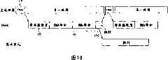
图10是对应于图7C的计时图。Figure 10 is a timing chart corresponding to Figure 7C.
图11表示如何使用同步寄存器的一个例子。Figure 11 shows an example of how to use the synchronization register.
图12表示如何使用同步寄存器的另一例子。Figure 12 shows another example of how to use the synchronization register.
图13表示如何使用同步寄存器的另一例子。Figure 13 shows another example of how to use the synchronization register.
图14表示处理两个指令串的方法。Figure 14 shows the method of processing two instruction strings.
图15是表示控制器21的程序的例子的数据流程图。FIG. 15 is a data flow diagram showing an example of a program of the
图16表示主处理器1的程序的一个例子。FIG. 16 shows an example of a program of the main processor 1 .
图17是表示根据第二实施例的控制器21的内部结构的方框图。FIG. 17 is a block diagram showing the internal structure of the
图18是表示图17中的专用电路32a的内部结构的例子的方框图。Fig. 18 is a block diagram showing an example of the internal configuration of the
图19是表示图17中的控制器21执行的程序的例子的流程图。FIG. 19 is a flowchart showing an example of a program executed by the
图20是表示根据本申请的处理器系统装入数字电视机中的情况的方框图。FIG. 20 is a block diagram showing a state where a processor system according to the present application is built into a digital television.
图21是表示根据本实施例的处理器系统装入视频记录器/播放器中的例子的方框图。Fig. 21 is a block diagram showing an example in which the processor system according to the present embodiment is built into a video recorder/player.
具体实施方式Detailed ways
下面参考附图,说明根据本发明一个实施例的处理器系统,DMA控制电路,DMA控制方法,DMA控制器用控制方法,图形处理方法和图形处理电路。A processor system, a DMA control circuit, a DMA control method, a control method for a DMA controller, a graphics processing method, and a graphics processing circuit according to an embodiment of the present invention will be described below with reference to the accompanying drawings.
(第一实施例)(first embodiment)
图1是表示根据本发明第一实施例的处理器系统的示意结构的方框图。图1中所示的处理器系统包括主处理器1,图形处理处理器2,主存储器3和I/O处理器4。FIG. 1 is a block diagram showing a schematic configuration of a processor system according to a first embodiment of the present invention. The processor system shown in FIG. 1 includes a main processor 1 , a graphics processing processor 2 , a main memory 3 and an I/O processor 4 .
主处理器1包括主处理器11,多个数字信号处理器(DSP)和控制与外部电路的输入/输出操作的I/O单元13、14和15。I/O单元13控制与主存储器3的输入/输出操作,I/O单元14控制与图形处理处理器2的输入/输出操作,I/O单元15控制与I/O处理器4的输入/输出操作。The main processor 1 includes a main processor 11, a plurality of digital signal processors (DSPs), and I/O units 13, 14, and 15 that control input/output operations with external circuits. The I/O unit 13 controls the input/output operation with the main memory 3, the I/O unit 14 controls the input/output operation with the graphics processing processor 2, and the I/O unit 15 controls the input/output operation with the I/O processor 4. output operation.
图形处理处理器2包括充当本实施例的特征部分的控制器21,执行与主处理器1的数据交换的I/O单元22,各种通用总线,例如PCI总线,控制视频数据、音频数据等的输入/输出操作的I/O单元23,和执行图形处理计算的图形处理单元24。The graphics processing processor 2 includes a
图形处理单元24包括把多边形的顶点信息转换成象素数据的象素转换器26,和处理象素数据的多个算术单元(DSP)27。The
I/O处理器4控制与通用总线,诸如HDD和DVD之类的外围设备,以及网络的连接。The I/O processor 4 controls connections to a general-purpose bus, peripheral devices such as HDD and DVD, and a network.
图2是表示图1中所示的图形处理处理器2的内部结构的细节的方框图。多个算术单元27中的每一个都包括由多个处理器构成的一个处理器群集28,和保存处理器群集28的处理结构的一个存储器29。处理器群集28中的多个处理器能够彼此并行地执行独立过程,并且能够执行一个过程,以致多个处理器群集28共享该过程。存储器29保存处理器群集28的执行结果。图2中所示的控制器21,象素转换器26,I/O单元22及23,和存储器29与公共总线30连接。FIG. 2 is a block diagram showing details of the internal structure of the graphics processing processor 2 shown in FIG. 1. Referring to FIG. Each of the plurality of
图3是表示控制器21的内部结构的例子的方框图。图3中所示的控制器21包括多个DMA控制器(DMAC)31,一个专用电路32,由多个通用处理器构成的一个控制处理器33,一个计时器34,一个中断单元35和一个存储器36。FIG. 3 is a block diagram showing an example of the internal configuration of the
DMA控制器31执行多个算术单元27之间的数据传输,以及多个算术单元27和存储器36之间的数据传输。专用电路32是专用于该系统的电路,执行关于DMA控制器31和算术单元27的启动控制。控制处理器33根据保存在存储器36中的程序代码,或者来自主处理器1的指令,控制专用电路32。计时器34执行时间管理,并根据需要指令中断单元35执行中断。中断单元35接收来自计时器34的信号,或者来自DMA控制器31或算术单元27的完成信号,对控制处理器33执行中断。The
图3中所示的专用电路32,计时器34,中断单元35和存储器36与本地网络37连接。主处理器1也通过I/O单元22与本地网络37连接。存储器36由例如嵌入式DRAM构成。提供例如30个以上的DMA控制器。The
图4是表示图3中的专用电路32的内部结构的例子的方框图。该方框图表示其中以控制处理器33的协处理器的形式,连接专用电路32的结构。图4中的专用电路32包括控制处理器I/O单元41,多个DMA寄存器42,一个DMA发布单元43,多个同步寄存器44,和一个同步寄存器控制单元45。FIG. 4 is a block diagram showing an example of the internal configuration of the
控制处理器I/O单元41与控制处理器33交换数据。DMA寄存器保存DMAC 31的操作所需的各种信息。DMA发布单元43执行把DMA寄存器42中的各种信息传送给DMAC31的过程。从其传送信息的特定DMA寄存器和向其传送信息的特定DMAC 31由控制处理器33确定。通过控制处理器I/O单元41,把所述特定DMA寄存器和特定DMAC 31通知DMA发布单元43。同步寄存器44保存DMAC 31和算术单元27的操作状态。同步寄存器控制单元45控制同步寄存器44的更新。The control processor I/
图5是表示图1的控制器21执行的程序的例子的流程图。该流程图表示当在主处理器1中准备的数据被DMA传送给图形处理处理器2中的存储器36时执行的程序。FIG. 5 is a flowchart showing an example of a program executed by the
当主处理器1准备将由图形处理处理器2处理的数据时,主处理器1把准备完成信号传送给图3中的本地网络37。该信号由图4中的同步寄存器控制单元45接收(步骤S1)。When the main processor 1 prepares data to be processed by the graphics processing processor 2, the main processor 1 transmits a preparation completion signal to the local network 37 in FIG. This signal is received by the synchronization
同步寄存器控制单元45更新同步寄存器44的值(步骤S2)。更具体地说,同步寄存器44被设置成代表主处理器1的数据传输的准备已完成的值。The synchronization
控制处理器33根据专用指令,通过控制处理器I/O单元41读取同步寄存器44的值,以确认主处理器1的准备已完成(步骤S3)。这里,所述专用指令表示一项任务。包括由控制处理器33和专用电路32执行的专用指令(任务)的指令串表示一个任务串。The
通过控制处理器I/O单元41,控制处理器33把DMAC 31的设置信息传送给DMA寄存器42(步骤S4)。By controlling the processor I/
控制处理器33根据专用指令,通过控制处理器I/O单元41启动DMA发布单元43,并指令DMA发布单元43把保存在DMA寄存器42中的DMAC 31的设置信息设置到每个DMAC 31中(步骤S5)。
之后,DMAC 31执行DMA传输。当DMA传输完成时,DMAC31向同步寄存器控制单元45通知DMA传输已完成(步骤S6)。同步寄存器控制单元45更新同步寄存器44(步骤S7)。After that, the
控制处理器33根据专用指令,通过控制处理器I/O单元41,读取同步寄存器的值,并确认DMA传输完成(步骤S8)。之后,控制处理器33通过控制处理器I/O单元41启动算术单元27,处理从主处理器1传送给图形处理处理器2中的存储器的数据(步骤S9)。The
如上所述,图4中的同步寄存器控制单元45监视同步寄存器44的值。定期监视通常被称为“轮询”。根据本实施例的同步寄存器控制单元45能够通过轮询,监视DMAC 31,算术单元27和主处理器1的操作。As mentioned above, the synchronization
代替用同步寄存器控制单元45监视同步寄存器44,控制处理器33可通过控制处理器I/O单元41监视同步寄存器44。Instead of monitoring the
这样,控制DMAC 31的命令被称为指令,每个命令由例如256位数据构成。专用电路32中的同步寄存器控制单元45和同步寄存器44用作任务调度器。In this way, commands to control the
更具体地说,任务包括与DMAC 31的数据传输控制相关的命令,与算术单元27的启动控制以及算术单元27的初始设置相关的命令,和与关于主处理器1的中断通知相关的命令。More specifically, the tasks include commands related to data transfer control of the
根据本实施例的专用电路32持续执行任务,直到称为阻挡任务(block task)的特殊任务被执行为止。阻挡任务是等待在所述阻挡任务之前发出的任务(DMA执行或者处理器群集的过程)的执行完成的任务。当阻挡任务被执行时,专用电路32等待,直到完成设定的任务的执行为止。The
图6A表示专用电路32执行的任务的例子,表示了其中执行任务A、B、C、D、E、F和G的例子。图6A中的任务被写成如图6B中所示的数据流程图。专用电路32执行任务A,等待作为阻挡任务的任务A的执行完成。当完成任务A的执行时,专用电路32并行执行任务F和B。专用电路32等待作为阻挡任务的任务F和B的执行完成。当完成任务F和B的执行时,专用电路32并行执行任务C和D。专用电路32等待作为阻挡任务的任务C和D的执行完成。当完成任务C和D的执行时,专用电路32执行任务E。专用电路32等待作为阻挡任务的任务E的执行完成。当完成任务E的执行时,专用电路32执行任务G。FIG. 6A shows examples of tasks performed by the
按照这种方式,图6B中的阻挡任务能够使多个DMA传输同步。In this way, the blocking task in Figure 6B is able to synchronize multiple DMA transfers.
本实施例的专用电路32能够借助除了DMA传输完成的通知之外的事件启动接下来的DMA传输。这里提及的事件是例如算术单元27的计算过程的完成,或者来自主处理器1的通知。The
图7A表示传统DMAC 31的第一操作,图7B表示传统DMAC 31的第二操作,图7C表示根据本实施例的DMAC的操作。图8是对应于图7A的计时图,图9是对应于图7B的计时图,图10是对应于图7C的计时图。FIG. 7A shows the first operation of the
图7A和8表示最普及的DMA传输。在完成某一DMA传输之后,执行下一DMA传输。这种情况下,如图8中所示,主处理器1(CPU)执行DMA的指定(t1),算术单元27的寄存器设置(t2),和算术单元27的执行的指定(t3)。DMAC 31执行由主处理器1指定的DMA命令。Figures 7A and 8 represent the most popular DMA transfers. After a certain DMA transfer is completed, the next DMA transfer is performed. In this case, as shown in FIG. 8, the main processor 1 (CPU) performs designation of DMA (t1), register setting of the arithmetic unit 27 (t2), and designation of execution of the arithmetic unit 27 (t3). The
在图7A和8中所示的例子中,与DMA传输相关的各种设置和指定,以及算术单元27的执行的指定由主处理器1完成。因此,主处理器1上的负载过大。于是,主处理器1执行另一过程的时段(t4)变短,从而主处理器1的性能降低。In the examples shown in FIGS. 7A and 8 , various settings and designations related to DMA transfer, and designation of execution of the
在图7B和9中所示的例子中,能够相互并行地执行多个DMA传输。但是,如图9中所示,主处理器1执行寄存器设置和算术单元27的起动的指定(时段t5)。根据所述指定,DMAC 31传输寄存器设置和算术单元27的起动的指定(时段t6)。该例子中,由于能够并行地对多个DMAC 31进行寄存器设置,因此当要进行寄存器设置的寄存器的数目较大时,能够减小主处理器1上的处理负载。但是,当只重新设置一些寄存器时,和图7A和8中的情况一样,主处理器1上的处理负载增大。In the examples shown in FIGS. 7B and 9, multiple DMA transfers can be performed in parallel with each other. However, as shown in FIG. 9 , the main processor 1 performs designation of register setting and activation of the arithmetic unit 27 (period t5 ). According to the designation, the
另一方面,在图7C和10中所示的实施例中,不仅只通过利用DMA传输的结束作为触发信号,进行下一DMA传输,而且还利用来自算术单元27或主处理器1的通知作为触发信号,执行下一DMA传输。DMAC 31能够执行算术单元27的寄存器设置,和算术单元27的执行的指定。更具体地说,如图10中所示,当主处理器1指定DMAC31执行DMA传输(时段t7)时,响应该指定,DMAC 31执行算术单元27的寄存器设置(时段t8),DMA传输(时段t9),和算术单元27的执行的指定(时段t10)。当完成计算过程时,算术单元27把计算过程的结束通知DMAC 31。On the other hand, in the embodiments shown in FIGS. 7C and 10, the next DMA transfer is performed not only by using the end of the DMA transfer as a trigger signal, but also using a notification from the
如图10中所示,由于DMAC 31控制DMA传输和控制算术单元27的执行,主处理器1能够向其它过程分配较长的时间。于是,能够提高主处理器1的性能。As shown in FIG. 10, since the
下面更详细地说明主处理器1的操作,以及图形处理处理器2中的控制器21的操作。主处理器1读取保存在主存储器3中的任务串,以便把任务串传送给图形处理处理器2中的存储器。该传输过程可由主处理器1的存储任务直接写入该存储器中,或者DMA传输可实现执行成任务之一。The operation of the main processor 1, and the operation of the
控制器21中的同步寄存器控制单元45把任务串的指针信息等设置到DMAC 31的DMA寄存器42中。根据DMA寄存器42的内容,DMA发布装置对每个DMAC 31执行各种设置。The synchronous
控制器21不仅能够执行DMAC 31的启动控制,而且能够执行算术单元27的启动控制。作为当控制器21控制算术单元27时使用的任务,已知的有两种任务,即设置任务和突跳任务(kick task)。设置任务是对算术单元27执行各种设置的任务。更具体地说,进行各种设置,以便显示诸如纹理或顶点之类的三维图像。突跳任务是指定算术单元27的开始执行的任务。The
如上所述,在同步寄存器44中,保存DMAC 31,算术单元27等的操作状态。主处理器1能够通过同步寄存器控制单元45,读取同步寄存器44的值。几种方法可被用作使用同步寄存器44的方法。图11、12和13中表示了这些方法中的一个典型方法。As described above, in the
在图11中,某一过程由控制器21执行(步骤S11)。处理结果由写任务写入同步寄存器44(步骤S12)。控制器21中断该任务的执行,直到从主处理器1收到阻挡取消通知为止(步骤S13)。当主处理器1定期进行同步寄存器44的轮询(步骤S13),以获得在写任务中,写入同步寄存器44中的值时,主处理器1把阻挡取消通知控制器21(步骤S15)。In FIG. 11, a certain process is executed by the controller 21 (step S11). The processing result is written into the
在图12中,控制器21借助突跳任务启动算术单元27(步骤S16),并中断该任务的执行,直到算术单元27中的过程结束为止(步骤S17)。由突跳任务启动的算术单元27执行某一过程(步骤S18)。当完成该过程时,算术单元27把完成通知传送给控制器21,并把返回值写入同步寄存器44(步骤S19)。接收完成通知的控制器21参考通用寄存器的值完成转移(branch)(步骤S20)。In FIG. 12, the
在图13中,控制器21执行某一过程(步骤S21)。当完成该过程时,中断该任务的执行,直到控制器21从主处理器1收到阻挡取消的通知为止(步骤S22)。主处理器1动态设置控制器21重新开始执行该任务的时间(步骤S23)。此时,主处理器1取消控制器21的阻挡,并把返回值写入同步寄存器44中(步骤ST24)。控制器21参考同步寄存器44的值完成转移(步骤ST25)。In FIG. 13, the
如上所述,控制器21能够同时执行多个任务串。作为所述执行的一个例子,下面说明一个程序,执行所述程序,以致数据从主存储器3传送到存储器中,数据的指针被设置到算术单元27中。这种情况下,控制器21同时执行两个任务串,并使任务串同步。所述同步由来自主处理器1的指定实现。As mentioned above, the
如图14中所示,假定存储器被分成四个区域(下面称为FIFO0-3)。在这两个任务串中的一个任务串(下面称为任务串1)中,主存储器3把数据传送给FIFO 0-3。在另一任务串(下面称为任务串2)中,数据从FIFO 0-3传送给算术单元27。As shown in FIG. 14, assume that the memory is divided into four areas (hereinafter referred to as FIFO0-3). In one of the two task strings (hereinafter referred to as task string 1), the main memory 3 transfers data to the FIFOs 0-3. In another task string (hereinafter referred to as task string 2), data is transferred from FIFO 0-3 to
任务串2实际上借助设置任务,执行对算术单元27的初始设置。算术单元27从存储器读取数据。The task string 2 actually performs the initial setting of the
图15是表示执行上述两个任务串1和2的控制器21的程序的例子的数据流程图。彼此并行地执行图15中的任务串1和任务串2。在任务串1中,数据被顺序从主存储器3传送给FIFO 0-3。之后,控制器21返回任务串1的顶部(步骤S31-S39)。每次完成向FIFO 0-3的数据传输过程时,该过程被中断。当控制器21从主处理器1收到阻挡取消的通知时,控制器21执行下一数据传输过程。FIG. 15 is a data flow diagram showing an example of a program of the
另一方面,在任务串2中,FIFO 0-3的地址被设置到算术单元27中,顺序重复指定算术单元27启动的过程,控制器21返回任务串2的顶部(步骤S41-S54)。在FIFO 0-3的地址被设置到算术单元27中之后,中断该过程。当主处理器1取消该阻挡时,执行下一过程。On the other hand, in the task string 2, the address of FIFO 0-3 is set in the
实现图15中的过程的主处理器1的程序的一个例子如图16中所示。An example of the program of the main processor 1 that realizes the process in FIG. 15 is shown in FIG. 16 .
按照这种方式,在第一实施例中,独立于主处理器1安排具有实现多个DMAC 31和多个算术单元27的启动控制的控制器21的图形处理处理器2,从而能够并行于在主处理器1中执行的过程,由控制器21完成DMAC 31的控制和算术单元27的启动指定。因此,能够减小主处理器上的处理负载。In this way, in the first embodiment, the graphics processing processor 2 having the
DMAC 31和算术单元27的启动指定也可由除DMA传输结束的通知之外的事件实现。因此,能够执行具有更高自由度的任务过程。The start designation of the
(第二实施例)(second embodiment)
在上述第一实施例中,说明了其中DMAC 31和算术单元27的启动由控制器处理器33和专用电路32控制的例子。但是,DMAC 31和算术单元27的启动控制可以只由专用电路32实现。In the first embodiment described above, an example in which the activation of the
图17是表示根据第二实施例的控制器21的内部结构的方框图。和图3相同的附图标记表示图17中的相同部分。下面主要说明图3和图17的不同之处。在图17的控制器21中,图3中的控制处理器33和专用电路32被集成为一个专用电路32a。FIG. 17 is a block diagram showing the internal structure of the
图17中的专用电路32a根据保存在存储器36中的程序代码,控制DMAC 31和算术单元27。The
图18是表示图17中的专用电路32a的内部结构的例子的方框图。图18中的专用电路32a包括一个任务取出解码器51,一个同步管理单元52,一个DMA发布单元43,多个同步寄存器44,和一个同步寄存器控制单元45。Fig. 18 is a block diagram showing an example of the internal configuration of the
任务取出解码器51解释保存在存储器36中的程序代码。同步管理单元52执行由任务取出解码器51解释的任务,并读取同步寄存器44的值,以便控制算术单元27和DMA发布单元43。The task fetch decoder 51 interprets the program code stored in the
图19是表示图17中的控制器21执行的程序的例子的流程图。下面主要说明图19中的流程图和图5中的流程图之间的不同过程。在同步寄存器控制单元45更新同步寄存器44的值(步骤S62)之后,同步管理单元52根据任务取出解码器51译解的任务,读取同步寄存器44的值(步骤S63)。按照这种方式,确定完成主处理器1的准备中,关于数据传输的准备。FIG. 19 is a flowchart showing an example of a program executed by the
同步管理单元52把各条信息设置到DMAC 31中,以便把将设置在DMAC 31中的各条信息(这种情况下,在主处理器1中准备的数据)传送给图形处理处理器2中的存储器(步骤S64)。The synchronization management unit 52 sets each piece of information into the
在DMAC 31被启动之后,当DMAC 31结束DMA传输时,完成信号被传送给同步寄存器控制单元45(步骤S65)。同步寄存器控制单元45更新同步寄存器44(步骤S66)。After the
根据任务取出解码器51译解的任务,同步管理单元52读取同步寄存器44的值(步骤S67),以确认DMAC 31的完成。Take out the task that decoder 51 deciphers according to task, synchronous management unit 52 reads the value of synchronous register 44 (step S67), to confirm the completion of
根据任务取出解码器51译解的任务,同步管理单元52启动算术单元27,开始处理从主处理器1传送给图形处理处理器2中的存储器的数据(步骤S68)。According to the task deciphered by the task fetch decoder 51, the synchronization management unit 52 activates the
如上所述,在第二实施例中,DMAC 31和算术单元27的启动控制只由专用电路32a实现。因此,能够获得比利用通用处理器获得的电路规模更小的电路规模,并且还能够获得低能耗。As described above, in the second embodiment, the activation control of the
上面的每个实施例举例说明了控制器21被安置在图形处理处理器2中的情况。但是,控制器21可在安置在图形处理处理器2之外。Each of the above embodiments exemplifies the case where the
上面的每个实施例举例说明了以不同的芯片的形式,形成主处理器1和图形处理处理器2的情况。但是,主处理器1和图形处理处理器2也可作为宏核心(macro core)形成于同一芯片上。这种情况下,控制器21最好被安排在图形处理处理器2中。但是,控制器21也可安排在图形处理处理器2之外。Each of the above embodiments exemplifies the case where the main processor 1 and the graphics processing processor 2 are formed in the form of different chips. However, the main processor 1 and the graphics processing processor 2 may also be formed on the same chip as a macro core. In this case, the
上面的每个实施例举例说明了控制器21专用于由图形处理处理器2执行的数据处理的情况。但是,控制器21也可控制另一DMAC,即,主处理器1中的DMAC。这种情况下,可与控制器21无关地在主处理器1中安排另一控制器。主处理器1中的DMAC和图形处理处理器2中的DMAC也可由共同的控制器控制。Each of the above embodiments exemplifies the case where the
如上所述的相同功能也可由代替控制器21的OS(操作系统)处理。The same functions as described above can also be handled by an OS (Operating System) instead of the
根据本发明的处理器系统可被装入游戏机,家用服务器,电视机,便携式信息设备等中。The processor system according to the present invention can be built into game machines, home servers, televisions, portable information devices, and the like.
图20是表示根据本申请的处理器系统装入数字电视机中的情况的方框图。充当该结构的一个例子的数字电视机包括控制通信信息的数字电路板55。数字电路板55包括实现和图1中一样的功能,控制图像信息的处理器系统56。更具体地说,处理器系统56包括发射/接收视频和通信信息的收发器电路(DEMUX)57,解码器电路58,处理器(CPU)59,图形处理电路(图形引擎)60,和数字格式转换器61。FIG. 20 is a block diagram showing a state where a processor system according to the present application is built into a digital television. A digital television serving as an example of this structure includes a digital circuit board 55 that controls communication information. The digital circuit board 55 includes a processor system 56 that performs the same functions as in FIG. 1, controlling image information. More specifically, the processor system 56 includes a transceiver circuit (DEMUX) 57 for transmitting/receiving video and communication information, a decoder circuit 58, a processor (CPU) 59, a graphics processing circuit (graphics engine) 60, and a digital format Converter 61.
图21是表示根据本实施例的处理器系统装入视频记录器/播放器中的例子的方框图。作为该结构的一个例子,视频记录器/播放器包括实现和图1中一样的功能,并且控制图像信息的图像信息控制电路62。更具体地说,图像信息控制电路62包括处理器(CPU)63,数字信号处理器(DSP)64,处理视频(图像)数据的处理器65,和处理音频数据的处理器66。Fig. 21 is a block diagram showing an example in which the processor system according to the present embodiment is built into a video recorder/player. As an example of this configuration, a video recorder/player includes an image
Claims (23)
Applications Claiming Priority (2)
| Application Number | Priority Date | Filing Date | Title |
|---|---|---|---|
| JP2004009351AJP2005202767A (en) | 2004-01-16 | 2004-01-16 | Processor system, DMA control circuit, DMA control method, DMA controller control method, image processing method, and image processing circuit |
| JP2004009351 | 2004-01-16 |
Publications (2)
| Publication Number | Publication Date |
|---|---|
| CN1641614Atrue CN1641614A (en) | 2005-07-20 |
| CN100454280C CN100454280C (en) | 2009-01-21 |
Family
ID=34631870
Family Applications (1)
| Application Number | Title | Priority Date | Filing Date |
|---|---|---|---|
| CNB2005100045075AExpired - Fee RelatedCN100454280C (en) | 2004-01-16 | 2005-01-14 | Processor system, DMA control circuit, DMA control method, control method for DMA controller, graphics processing method and graphics processing circuit |
Country Status (6)
| Country | Link |
|---|---|
| US (1) | US7627697B2 (en) |
| EP (1) | EP1557764A3 (en) |
| JP (1) | JP2005202767A (en) |
| KR (1) | KR100733943B1 (en) |
| CN (1) | CN100454280C (en) |
| TW (1) | TWI276965B (en) |
Cited By (4)
| Publication number | Priority date | Publication date | Assignee | Title |
|---|---|---|---|---|
| CN102789438A (en)* | 2011-05-16 | 2012-11-21 | 夏普株式会社 | Dma control device and image forming apparatus |
| CN104717433A (en)* | 2015-03-27 | 2015-06-17 | 电子科技大学 | Distributed transmission device for video stream signal processing system |
| CN110069432A (en)* | 2018-01-22 | 2019-07-30 | 华大半导体有限公司 | Peripheral circuit interconnection system and its interlock method with data processing function |
| CN112749112A (en)* | 2020-12-31 | 2021-05-04 | 无锡众星微系统技术有限公司 | Hardware flow structure |
Families Citing this family (31)
| Publication number | Priority date | Publication date | Assignee | Title |
|---|---|---|---|---|
| US9015397B2 (en)* | 2012-11-29 | 2015-04-21 | Sandisk Technologies Inc. | Method and apparatus for DMA transfer with synchronization optimization |
| US7743376B2 (en)* | 2004-09-13 | 2010-06-22 | Broadcom Corporation | Method and apparatus for managing tasks in a multiprocessor system |
| JP4723313B2 (en)* | 2005-08-24 | 2011-07-13 | パナソニック株式会社 | Image processing device |
| JP4530971B2 (en) | 2005-11-07 | 2010-08-25 | 株式会社ソニー・コンピュータエンタテインメント | Startup processing apparatus, DMA transfer system, and DMA transfer method |
| JP4687553B2 (en)* | 2006-04-28 | 2011-05-25 | 富士ゼロックス株式会社 | Image processing device |
| JP4893154B2 (en)* | 2006-08-21 | 2012-03-07 | 富士通セミコンダクター株式会社 | Image processing apparatus and image processing method |
| KR20080105390A (en)* | 2007-05-30 | 2008-12-04 | 삼성전자주식회사 | Method and apparatus for controlling instructions used in flash memory |
| JP2008299610A (en)* | 2007-05-31 | 2008-12-11 | Toshiba Corp | Multiprocessor |
| JP5181907B2 (en)* | 2008-07-31 | 2013-04-10 | 株式会社リコー | Image processing apparatus, image processing control method, image processing control program, and recording medium |
| US8732350B2 (en)* | 2008-12-19 | 2014-05-20 | Nvidia Corporation | Method and system for improving direct memory access offload |
| US9208108B2 (en)* | 2008-12-19 | 2015-12-08 | Nvidia Corporation | Method and system for improved flash controller commands selection |
| US8694750B2 (en)* | 2008-12-19 | 2014-04-08 | Nvidia Corporation | Method and system for data structure management |
| JP2011070259A (en)* | 2009-09-24 | 2011-04-07 | Mitsubishi Electric Corp | Data transfer device and data transfer method |
| US9536341B1 (en)* | 2009-10-19 | 2017-01-03 | Nvidia Corporation | Distributing primitives to multiple rasterizers |
| FR2953308B1 (en)* | 2009-12-01 | 2011-12-09 | Bull Sas | SYSTEM FOR AUTHORIZING DIRECT TRANSFERS OF DATA BETWEEN MEMORIES OF SEVERAL ELEMENTS OF THIS SYSTEM |
| FR2953307B1 (en)* | 2009-12-01 | 2011-12-16 | Bull Sas | MEMORY DIRECT ACCESS CONTROLLER FOR DIRECT TRANSFER OF DATA BETWEEN MEMORIES OF MULTIPLE PERIPHERAL DEVICES |
| US8683293B2 (en)* | 2009-12-16 | 2014-03-25 | Nvidia Corporation | Method and system for fast two bit error correction |
| US20110161553A1 (en)* | 2009-12-30 | 2011-06-30 | Nvidia Corporation | Memory device wear-leveling techniques |
| US9594675B2 (en)* | 2009-12-31 | 2017-03-14 | Nvidia Corporation | Virtualization of chip enables |
| JP2011159165A (en)* | 2010-02-02 | 2011-08-18 | Fujitsu Ltd | Parallel computer system and method and program for controlling the same |
| US9465728B2 (en) | 2010-11-03 | 2016-10-11 | Nvidia Corporation | Memory controller adaptable to multiple memory devices |
| GB2495959A (en)* | 2011-10-26 | 2013-05-01 | Imagination Tech Ltd | Multi-threaded memory access processor |
| US9336108B2 (en) | 2013-01-24 | 2016-05-10 | Xcerra Corporation | Scalable test platform |
| US9459978B2 (en) | 2013-01-24 | 2016-10-04 | Xcerra Corporation | Automated test platform utilizing segmented data sequencers to provide time controlled test sequences to device under test |
| US9430348B2 (en) | 2013-01-24 | 2016-08-30 | Xcerra Corporation | Scalable test platform in a PCI express environment with direct memory access |
| US9213616B2 (en)* | 2013-01-24 | 2015-12-15 | Xcerra Corporation | Automated test platform utilizing status register polling with temporal ID |
| US9430349B2 (en) | 2013-01-24 | 2016-08-30 | Xcerra Corporation | Scalable test platform in a PCI express environment with direct memory access |
| KR102415995B1 (en)* | 2015-09-30 | 2022-06-30 | 엘지디스플레이 주식회사 | Image processor and display device |
| CN105847180A (en)* | 2016-03-25 | 2016-08-10 | 深圳深宝电器仪表有限公司 | DMA configuration mode and interrupting method based on ADSP-BF60x network communication |
| JP7137058B2 (en)* | 2018-09-04 | 2022-09-14 | 富士通株式会社 | Arithmetic processing device, information processing device, and control method for information processing device |
| JP7463785B2 (en)* | 2020-03-18 | 2024-04-09 | 富士フイルムビジネスイノベーション株式会社 | Information processing device |
Family Cites Families (24)
| Publication number | Priority date | Publication date | Assignee | Title |
|---|---|---|---|---|
| JPS57111722A (en)* | 1980-12-29 | 1982-07-12 | Fujitsu Ltd | Dma transfer control system |
| JP2900359B2 (en) | 1986-10-30 | 1999-06-02 | 株式会社日立製作所 | Multiprocessor system |
| JPS6478184A (en)* | 1987-06-24 | 1989-03-23 | Nippon Kokan Kk | Method and device for deriving length of tubular body by utilizing acoustic wave |
| US4862407A (en) | 1987-10-05 | 1989-08-29 | Motorola, Inc. | Digital signal processing apparatus |
| US5315708A (en)* | 1990-02-28 | 1994-05-24 | Micro Technology, Inc. | Method and apparatus for transferring data through a staging memory |
| DE69229657T2 (en)* | 1991-06-19 | 1999-12-02 | Hewlett-Packard Co., Palo Alto | Co-processor supporting architecture for a processor that has no additional processor capability |
| US5666520A (en) | 1993-03-29 | 1997-09-09 | Hitachi, Ltd. | Graphics display system including graphics processor having a register storing a series of vertex data relating to a polygonal line |
| US6331856B1 (en) | 1995-11-22 | 2001-12-18 | Nintendo Co., Ltd. | Video game system with coprocessor providing high speed efficient 3D graphics and digital audio signal processing |
| US5894586A (en) | 1997-01-23 | 1999-04-13 | Xionics Document Technologies, Inc. | System for providing access to memory in which a second processing unit is allowed to access memory during a time slot assigned to a first processing unit |
| JPH10334037A (en)* | 1997-05-30 | 1998-12-18 | Sanyo Electric Co Ltd | Communication dma device |
| JPH1165989A (en) | 1997-08-22 | 1999-03-09 | Sony Computer Entertainment:Kk | Information processor |
| KR19990043773A (en)* | 1997-11-29 | 1999-06-15 | 정선종 | Direct memory access controller |
| DE69919059T2 (en) | 1998-02-04 | 2005-01-27 | Texas Instruments Inc., Dallas | Data processing system with a digital signal processor and a coprocessor and data processing method |
| US6202106B1 (en) | 1998-09-09 | 2001-03-13 | Xilinx, Inc. | Method for providing specific knowledge of a structure of parameter blocks to an intelligent direct memory access controller |
| EP1061439A1 (en) | 1999-06-15 | 2000-12-20 | Hewlett-Packard Company | Memory and instructions in computer architecture containing processor and coprocessor |
| US6421744B1 (en) | 1999-10-25 | 2002-07-16 | Motorola, Inc. | Direct memory access controller and method therefor |
| JP2001216227A (en) | 2000-02-02 | 2001-08-10 | Hitachi Ltd | Interface control device, interface control method, and external storage subsystem |
| JP2002163239A (en)* | 2000-11-22 | 2002-06-07 | Toshiba Corp | Multiprocessor system and control method thereof |
| US6820142B2 (en)* | 2000-12-14 | 2004-11-16 | International Business Machines Corporation | Token based DMA |
| US6779049B2 (en)* | 2000-12-14 | 2004-08-17 | International Business Machines Corporation | Symmetric multi-processing system with attached processing units being able to access a shared memory without being structurally configured with an address translation mechanism |
| US6865631B2 (en)* | 2000-12-14 | 2005-03-08 | International Business Machines Corporation | Reduction of interrupts in remote procedure calls |
| JP3895610B2 (en)* | 2001-03-21 | 2007-03-22 | 株式会社リコー | Image forming apparatus and image forming method |
| JP4144240B2 (en)* | 2002-04-12 | 2008-09-03 | セイコーエプソン株式会社 | Control apparatus and control method |
| US7478390B2 (en)* | 2003-09-25 | 2009-01-13 | International Business Machines Corporation | Task queue management of virtual devices using a plurality of processors |
- 2004
- 2004-01-16JPJP2004009351Apatent/JP2005202767A/enactivePending
- 2004-07-23USUS10/896,887patent/US7627697B2/ennot_activeExpired - Fee Related
- 2004-08-03EPEP04018358Apatent/EP1557764A3/ennot_activeWithdrawn
- 2004-12-22TWTW093140152Apatent/TWI276965B/ennot_activeIP Right Cessation
- 2005
- 2005-01-14KRKR1020050003827Apatent/KR100733943B1/ennot_activeExpired - Fee Related
- 2005-01-14CNCNB2005100045075Apatent/CN100454280C/ennot_activeExpired - Fee Related
Cited By (6)
| Publication number | Priority date | Publication date | Assignee | Title |
|---|---|---|---|---|
| CN102789438A (en)* | 2011-05-16 | 2012-11-21 | 夏普株式会社 | Dma control device and image forming apparatus |
| CN104717433A (en)* | 2015-03-27 | 2015-06-17 | 电子科技大学 | Distributed transmission device for video stream signal processing system |
| CN110069432A (en)* | 2018-01-22 | 2019-07-30 | 华大半导体有限公司 | Peripheral circuit interconnection system and its interlock method with data processing function |
| CN110069432B (en)* | 2018-01-22 | 2023-03-24 | 小华半导体有限公司 | Peripheral circuit interconnection system with data processing function and linkage method thereof |
| CN112749112A (en)* | 2020-12-31 | 2021-05-04 | 无锡众星微系统技术有限公司 | Hardware flow structure |
| CN112749112B (en)* | 2020-12-31 | 2021-12-24 | 无锡众星微系统技术有限公司 | Hardware flow structure |
Also Published As
| Publication number | Publication date |
|---|---|
| EP1557764A3 (en) | 2006-07-26 |
| KR20050075722A (en) | 2005-07-21 |
| US7627697B2 (en) | 2009-12-01 |
| US20050160200A1 (en) | 2005-07-21 |
| TW200540634A (en) | 2005-12-16 |
| EP1557764A2 (en) | 2005-07-27 |
| TWI276965B (en) | 2007-03-21 |
| CN100454280C (en) | 2009-01-21 |
| JP2005202767A (en) | 2005-07-28 |
| KR100733943B1 (en) | 2007-06-29 |
Similar Documents
| Publication | Publication Date | Title |
|---|---|---|
| CN1641614A (en) | Processor system, DMA control circuit, DMA control method, control method for DMA controller, graphic processing method, and graphic processing circuit | |
| CN1107287C (en) | Information processing apparatus and information processing method | |
| CN100336075C (en) | Apparatus, method and system utilizing a graphics rendering engine with a time allocator | |
| CN1828563A (en) | Processor and information processing method | |
| CN1862515A (en) | Data trnasfer apparatus, data transfer method, and program | |
| CN1279469C (en) | System and method for data synchronization for computer architecture for braadband networks | |
| CN1107923C (en) | Information processing device and method thereof | |
| CN1991905A (en) | Synchronization methods for graphics processing units and fence/wait synchronization components | |
| CN1106609C (en) | Method and apparatus for configuring multiple agents in a computer system | |
| CN1518705A (en) | processor structure | |
| CN1811718A (en) | Processor and information processing method | |
| CN1522405A (en) | Data processing device and method of synchronizing first and second processing means in a data processing device | |
| CN1806231A (en) | Methods and apparatus for providing a software implemented cache memory | |
| CN1991768A (en) | Internal sequencer based on instruction set architecture for communicating with different kinds of resources | |
| CN1255765C (en) | Data communication system and method | |
| CN1892630A (en) | Data transfer device which executes dma transfer, semiconductor integrated circuit device and data transfer method | |
| CN1181550A (en) | Microprocessor and multiple processors system | |
| CN1591374A (en) | Dma transfer controller | |
| CN102214085A (en) | Microcomputer and interrupt control method | |
| CN1183462C (en) | Data processing apparatus with variable pipeline stages | |
| CN1262934C (en) | System integration agents with different resource access schemes | |
| CN1719375A (en) | microprocessor | |
| CN1637712A (en) | Apparatus and method for interrupt control | |
| CN1945541A (en) | Processing operation information transfer control system and method | |
| CN1866233A (en) | Signal processing apparatus, signal processing system and signal processing method |
Legal Events
| Date | Code | Title | Description |
|---|---|---|---|
| C06 | Publication | ||
| PB01 | Publication | ||
| C10 | Entry into substantive examination | ||
| SE01 | Entry into force of request for substantive examination | ||
| C14 | Grant of patent or utility model | ||
| GR01 | Patent grant | ||
| CF01 | Termination of patent right due to non-payment of annual fee | Granted publication date:20090121 Termination date:20130114 | |
| CF01 | Termination of patent right due to non-payment of annual fee |