CN1638067A - Structures and methods for making strained mosfets - Google Patents
Structures and methods for making strained mosfetsDownload PDFInfo
- Publication number
- CN1638067A CN1638067ACNA2005100042715ACN200510004271ACN1638067ACN 1638067 ACN1638067 ACN 1638067ACN A2005100042715 ACNA2005100042715 ACN A2005100042715ACN 200510004271 ACN200510004271 ACN 200510004271ACN 1638067 ACN1638067 ACN 1638067A
- Authority
- CN
- China
- Prior art keywords
- strained
- film
- layer
- forming
- relaxed sige
- Prior art date
- Legal status (The legal status is an assumption and is not a legal conclusion. Google has not performed a legal analysis and makes no representation as to the accuracy of the status listed.)
- Granted
Links
Images


Classifications
- H—ELECTRICITY
- H10—SEMICONDUCTOR DEVICES; ELECTRIC SOLID-STATE DEVICES NOT OTHERWISE PROVIDED FOR
- H10D—INORGANIC ELECTRIC SEMICONDUCTOR DEVICES
- H10D30/00—Field-effect transistors [FET]
- H10D30/60—Insulated-gate field-effect transistors [IGFET]
- H10D30/62—Fin field-effect transistors [FinFET]
- H—ELECTRICITY
- H10—SEMICONDUCTOR DEVICES; ELECTRIC SOLID-STATE DEVICES NOT OTHERWISE PROVIDED FOR
- H10D—INORGANIC ELECTRIC SEMICONDUCTOR DEVICES
- H10D30/00—Field-effect transistors [FET]
- H10D30/01—Manufacture or treatment
- H10D30/021—Manufacture or treatment of FETs having insulated gates [IGFET]
- H10D30/024—Manufacture or treatment of FETs having insulated gates [IGFET] of fin field-effect transistors [FinFET]
- H—ELECTRICITY
- H10—SEMICONDUCTOR DEVICES; ELECTRIC SOLID-STATE DEVICES NOT OTHERWISE PROVIDED FOR
- H10D—INORGANIC ELECTRIC SEMICONDUCTOR DEVICES
- H10D30/00—Field-effect transistors [FET]
- H10D30/60—Insulated-gate field-effect transistors [IGFET]
- H10D30/791—Arrangements for exerting mechanical stress on the crystal lattice of the channel regions
- H—ELECTRICITY
- H10—SEMICONDUCTOR DEVICES; ELECTRIC SOLID-STATE DEVICES NOT OTHERWISE PROVIDED FOR
- H10D—INORGANIC ELECTRIC SEMICONDUCTOR DEVICES
- H10D30/00—Field-effect transistors [FET]
- H10D30/60—Insulated-gate field-effect transistors [IGFET]
- H10D30/67—Thin-film transistors [TFT]
- H10D30/674—Thin-film transistors [TFT] characterised by the active materials
- H10D30/6741—Group IV materials, e.g. germanium or silicon carbide
- H10D30/6748—Group IV materials, e.g. germanium or silicon carbide having a multilayer structure or superlattice structure
Landscapes
- Thin Film Transistor (AREA)
- Insulated Gate Type Field-Effect Transistor (AREA)
- Recrystallisation Techniques (AREA)
Abstract
Translated fromChineseDescription
Translated fromChinese发明领域field of invention
本发明涉及制造具有应变Si形成的竖直栅极的MOSFET,尤其涉及制造具有应变Si形成的竖直栅极的单栅极和双栅极MOSFET和翅片式FET。The present invention relates to the fabrication of MOSFETs with vertical gates formed of strained Si, and more particularly to the fabrication of single-gate and double-gate MOSFETs and finned FETs with vertical gates formed of strained Si.
背景技术Background technique
随着半导体器件的缩小,传统的器件制造技术已经接近其尺寸缩放的实用极限。例如,当沟道的长度缩小到约50nm之下时,器件开始表现出短沟道效应,包括对于缩短的沟道长度,阈值电压下降。可以通过更高的掺杂浓度来减轻不需要的短沟道效应,但更高的掺杂浓度导致产生不需要的载流子迁移率下降的效应,增大了寄生结电容,并且如果掺杂浓度过高,会增大亚阈值偏移。As semiconductor devices shrink, conventional device fabrication techniques are approaching their practical limits for size scaling. For example, when the length of the channel shrinks below about 50 nm, the device begins to exhibit short channel effects, including a drop in threshold voltage for the shortened channel length. Undesirable short channel effects can be mitigated by higher doping concentrations, but higher doping concentrations lead to unwanted carrier mobility drop effects, increased parasitic junction capacitance, and if doped Too high a concentration increases the subthreshold shift.
一种使短沟道和逆短沟道效应最小化的方法包括通过良好控制的注入和退火形成最优的掺杂型面。然而,仔细控制注入和退火增加了制造工艺成本,并且随着沟道长度的进一步减小,其有效性最终受到限制。还出现了由于栅极氧化物的厚度和源/漏极结深度的限制造成的尺寸缩放限制,而削弱了较小器件的功能。One approach to minimize short-channel and inverse short-channel effects involves forming an optimal doping profile through well-controlled implantation and annealing. However, carefully controlled implantation and annealing add to the cost of the fabrication process, and as the channel length decreases further, its effectiveness is ultimately limited. There are also scaling limitations due to limitations in gate oxide thickness and source/drain junction depth, impairing the functionality of smaller devices.
另一种获得进一步减小的尺寸的方法包括制造的沟道型面的困难。这样的型面包括双栅极,三栅极,四栅极,ω栅极,π栅极和翅片式FET的MOSFET设计。这些设计中有些受到比如导致增大寄生电容的栅极对准误差等的设计问题困扰。Another way to achieve further reduced dimensions involves difficulties in the manufactured channel profile. Such profiles include double-gate, tri-gate, quad-gate, ω-gate, π-gate and FinFET MOSFET designs. Some of these designs suffer from design issues such as gate alignment errors that lead to increased parasitic capacitance.
另一种避免某些尺寸缩放问题的可能方法是通过改进材料的性能来改进器件的性能。例如,应变Si产生了更高的载流子迁移率,导致形成更快和/或更慢的功率消耗器件。由于应变Si晶体结构的变化(即,其对称和晶格常数由于其应变状态而不同),应变Si薄膜具有优于体式Si的电性能。具体而言,应变Si可以具有更高的电子和空穴迁移率,它们分别转变成n型和p型晶体管的更高的驱动电流能力。因此,包含应变Si的器件可以具有改善的性能,而不必要减小器件的尺寸。然而,在应变Si的确允许进一步降低尺寸的情况下,性能的提高还可以进一步改善。Another possible way to avoid some of the scaling problems is to improve the performance of the device by improving the properties of the material. For example, strained Si yields higher carrier mobility, leading to faster and/or slower power dissipating devices. Due to the change in the strained Si crystal structure (ie, its symmetry and lattice constants are different due to its strained state), strained Si thin films have better electrical properties than bulk Si. Specifically, strained Si can have higher electron and hole mobilities, which translate into higher drive current capabilities for n-type and p-type transistors, respectively. Therefore, devices containing strained Si may have improved performance without necessarily reducing the size of the device. However, where strained Si does allow for further size reductions, the performance gains can be further improved.
然而,应当指出,在通过利用应变Si实现高性能器件的过程中重要的指标是制造出低缺陷密度的应变Si薄膜。尤其是,减少应变Si薄膜中的位错数量特别重要,以便降低泄漏,改进载流子迁移率。However, it should be pointed out that an important indicator in the process of realizing high-performance devices by utilizing strained Si is to fabricate strained Si films with low defect density. In particular, it is particularly important to reduce the number of dislocations in strained Si films in order to reduce leakage and improve carrier mobility.
在晶格参数不同于Si的衬底上生长硅膜,产生了应变Si薄膜。因此,应变Si薄膜的缺陷数量可以与下方的生长所述薄膜的衬底中缺陷的数量成比例。在Si沟道中位错数量的增加可能增大器件在处于“关断”阶段时的漏电流。当不适当地形成时,应变Si薄膜可能包含大量的缺陷,并且随后的应变Si薄膜将表现出较差的性能,因此基本上抵消了使用应变Si薄膜的任何优点。Growing silicon films on substrates with lattice parameters different from Si produces strained Si films. Thus, the number of defects in a strained Si film can be proportional to the number of defects in the underlying substrate growing the film. An increase in the number of dislocations in the Si channel may increase the leakage current of the device when it is in the "off" phase. When improperly formed, strained Si films may contain a large number of defects, and subsequent strained Si films will exhibit poorer performance, thus essentially negating any advantage of using strained Si films.
因此,为了进一步降低半导体器件尺寸和功率需求,希望生产具有最少缺陷比如位错的应变Si薄膜。具有较少缺陷的应变Si薄膜可以改善半导体器件的性能。Therefore, in order to further reduce semiconductor device size and power requirements, it is desirable to produce strained Si thin films with minimal defects such as dislocations. Strained Si thin films with fewer defects can improve the performance of semiconductor devices.
发明内容Contents of the invention
在本发明的一方面,一种方法,包含在衬底上形成弛豫SiGe块,并且在所述衬底上至少邻近所述弛豫SiGe块一侧形成应变Si薄膜。所述方法还包括位于所述应变Si薄膜一侧形成栅极氧化物,从而形成应变沟道区。In one aspect of the invention, a method includes forming a relaxed SiGe bulk on a substrate, and forming a strained Si film on the substrate at least adjacent to one side of the relaxed SiGe bulk. The method also includes forming a gate oxide on one side of the strained Si film, thereby forming a strained channel region.
在另一方面,本发明包括一种方法,包含在氧化物衬底上形成弛豫SiGe块,并且在所述弛豫SiGe块顶部上形成第一氮化物分隔层。在所述氧化物衬底上邻近所述弛豫SiGe块的第一侧和所述第一氮化物分隔层的一侧形成第二氮化物分隔层,且在所述弛豫SiGe块的第二侧外延地形成应变Si薄膜。In another aspect, the invention includes a method comprising forming a relaxed SiGe bulk on an oxide substrate, and forming a first nitride spacer layer on top of the relaxed SiGe bulk. A second nitride spacer layer is formed on the oxide substrate adjacent to the first side of the relaxed SiGe block and one side of the first nitride spacer layer, and on the second side of the relaxed SiGe block The strained Si film is formed epitaxially.
在另一方面,本发明包括用于半导体器件的沟道,包含在非导电衬底上竖直定向的应变Si形成的翅片。In another aspect, the invention includes a channel for a semiconductor device comprising fins formed of vertically oriented strained Si on a non-conductive substrate.
附图说明Description of drawings
图1-8示出了形成本发明的实施例的步骤。1-8 illustrate steps in forming an embodiment of the invention.
图9-14示出了形成本发明的器件的步骤;Figures 9-14 illustrate the steps of forming a device of the present invention;
图15-19示出了形成本发明的实施例的另一些步骤。15-19 illustrate further steps in forming an embodiment of the present invention.
具体实施方式Detailed ways
本发明涉及形成具有应变Si形成的沟道的MOSFET。在本发明中,通过产生应变Si薄膜而提高了晶体管的性能。由于应变Si的尺寸较小,当比如通过外延生长技术形成时,通常缺陷(例如,位错)的密度非常低。这种低缺陷薄膜可以通过在氧化物晶片上驰豫SiGe上形成竖直的SiGe条或块而形成。在SiGe条或块的一侧可以用氮化物覆盖。竖直的SiGe条或块的另一侧可以使用选择性外延生长工艺由小尺寸的Si薄膜覆盖。由于与所述SiGe衬底的晶格常数不匹配,所述Si薄膜将会发生应变。由于Si膜的尺寸较小,和SiGe衬底的驰豫结构,减轻了形成位错的倾向。完成后,应变Si可以进行进一步处理,从而形成多种类型的MOSFET,比如具有单栅极,双栅极或更多栅极的翅片式FET。The present invention relates to the formation of MOSFETs with strained Si formed channels. In the present invention, the performance of the transistor is improved by creating a strained Si film. Due to the small size of strained Si, typically the density of defects (eg, dislocations) is very low when formed, eg, by epitaxial growth techniques. Such low-defect films can be formed by forming vertical SiGe stripes or blocks on relaxed SiGe on an oxide wafer. One side of the SiGe strip or block can be covered with nitride. The other side of the vertical SiGe strips or blocks can be covered by a small-scale Si film using a selective epitaxial growth process. Due to the lattice constant mismatch with the SiGe substrate, the Si film will be strained. Due to the smaller size of the Si film and the relaxed structure of the SiGe substrate, the tendency to form dislocations is reduced. Once complete, the strained Si can be further processed to form various types of MOSFETs, such as finned FETs with single gates, double gates or more gates.
图1示出了在氧化物晶片10上的弛豫SiGe层12。尽管在该示例中使用氧化物晶片,但可以使用适于半导体器件制造的任何非导电衬底。弛豫SiGe层12可以通过任何本领域公知的适当方法在氧化物晶片10上形成,这些方法比如晶片键合或氧注入退火。在一个实施例中,SiGe层12的厚度在30nm和80nm之间,但其他厚度也在本发明的考虑之中。FIG. 1 shows a
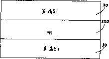
图2示出了淀积在弛豫SiGe层12上的薄氧化物层14。第一多晶硅层16在氧化物层14上形成。然后,光致抗蚀剂18淀积在第一多晶硅层16上,且形成图案,而使第一多晶硅层16的一部分被光致抗蚀剂18覆盖,第一多晶硅层16的一部分被暴露。薄氧化物层14的典型厚度约5至20nm,第一多晶硅层16为40nm至100nm。每层都通过本领域公知的方法制成。FIG. 2 shows a
图3示出了蚀刻工艺的结果,其中第一多晶硅层16的暴露部分和下方的薄氧化物层14被蚀刻掉,留下第一多晶硅16的一部分。蚀刻工艺使用公知的方法来选择性地蚀刻多晶硅和氧化物。光致抗蚀剂层18也在第一多晶硅16和氧化物层14在蚀刻之后被去除。因此,SiGe层12的第一部分暴露,SiGe层12的第二部分被薄氧化物层14和第一多晶硅层16覆盖。接着,使用本领域公知的任何氮化物形成工艺在SiGe层12顶部邻接薄氧化物层14的边缘和第一多晶硅层16形成第一氮化物分隔层20。FIG. 3 shows the result of an etching process in which exposed portions of the
图4示出了另一蚀刻步骤,其中使用类似于参照图3描述的蚀刻工艺对暴露的SiGe层12进行选择性蚀刻。在图4中,没有被第一氮化物分隔层20、和薄氧化物层14以及第一多晶硅层16覆盖的驰豫SiGe层12的所述部分,被蚀刻掉,而露出下面的氧化物晶片10的一部分。然后在所述氧化物晶片10的暴露部分上邻接蚀刻的驰豫SiGe层12的边缘形成第二氮化物分隔层22。第一氮化物分隔层20邻近第二氮化物分隔层22。FIG. 4 shows another etching step in which the exposed
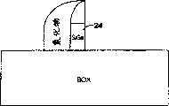
图5示出了选择性地蚀刻第一多晶硅层16和薄氧化物层14的剩余部分的结果。在薄氧化物层14和第一多晶硅层16下面的驰豫SiGe层的所述部分在该工艺中被蚀刻掉。因此,从氧化物晶片10顶部的初始驰豫SiGe层12留下被成形为SiGe块24的驰豫SiGe。SiGe块24在一侧被第二氮化物层22围绕,在顶部被第一氮化物分隔层20围绕,使SiGe块24的一侧暴露。FIG. 5 shows the result of selectively etching the
图6示出了在SiGe块24的暴露侧上外延生长的“应变”Si薄膜26。使用选择性地生长工艺,而使Si薄膜26仅在SiGe块24的暴露部分上生长。在该工艺中,Si薄膜26具有大于其厚度的高度,且在氧化物晶片10的表面上竖直定向。因为Si薄膜26可以以基本上任何纵横比(高度除以厚度)形成,包括大于1的那些纵横比,所以Si薄膜26可以表现为在氧化物晶片10上竖直定向的“翅片”。FIG. 6 shows a "strained"
此外,Si薄膜26可以与SiGe块24的高度大致相同。因此,Si薄膜26的高度可以通过调节驰豫SiGe层12的层高度进行控制。SiGe层12的高度可以在其通过本领域公知的方法形成的过程中进行控制。而且,Si薄膜26的厚度可以在通过器件制造领域公知的适当方法进行的生长工艺中控制。Si薄膜26的厚度可以约50(埃)至约200,但在需要的情况下可以使用其他的厚度。In addition, the
Si薄膜26可以用作从缺陷数目减少和/或尺寸较小的沟道而受益的实际上任何类型的器件中的半导体器件的沟道。因此,可以在Si沟道的一部分上形成至少一个栅极氧化物,其中在所述栅极氧化物两侧的Si薄膜26上分别形成源极区域/漏极区域。所形成的结构,因为它是竖直定向的,所以可以从衬底上方接近沟道两侧和顶部。这种几何形状可以使栅极氧化物围绕所述沟道,且可以在断路状态所述沟道几乎全部耗尽。也可以接近源极/漏极区域的两侧,以便更好地掺杂和更好的引线连通性。
通过在驰豫SiGe块24的表面上生长Si薄膜26,减少了在所形成的Si薄膜26上的缺陷数目,比如位错。Si薄膜26中的位错也最小化,因为仅生长小尺寸的薄膜。此外,应变Si薄膜由于其晶格在SiGe晶格上形成而实现其内部应变。即,SiGe块24具有比Si薄膜的大的晶格常数(原子之间的不同尺寸),即单独地,Si通常具有小于SiGe的晶格,因为Si材料的晶格常数与SiGe的晶格常数不匹配。然而,在本发明的结构中,Si层的晶格将趋于匹配SiGe的晶格。由于Si的晶格(通常较小)与SiGe掩模匹配,所以Si层处于张应力下。即,SiGe掩模将试图获得平衡状态,这样导致在SiGe上形成的Si侧壁层产生应力。这一体积的应力硅可以用作应变沟道。因此,Si薄膜26可以描述为低缺陷应变Si翅片或沟道。By growing the Si
图7示出了使用离子注入在Si薄膜26的暴露侧上形成栅极氧化物28。例如可以使用Vt(阈值电压)离子注入技术,且注入角可以朝侧面的栅极氧化物28倾斜。栅极氧化物28的示例厚度约9至约20,但在需要时可以形成其他厚度。也可以使用高“k”材料,比如HfO2,来代替氧化物作为栅极电介质。FIG. 7 shows the formation of
图8示出了淀积在第一和第二氮化物分隔层20和22、SiGe块24、Si薄膜26和栅极氧化物28上的第二多晶硅层30。虽然第二多晶硅层30示为共形层,但可以形成非共形层,或具有根据器件形成的后续步骤需要而在共形和非共形之间某处的形状的层。例如,多晶硅层30的厚度可以从约700至约1500。FIG. 8 shows
从图8所示的结构可知,可以制造各种器件,包括例如应变SiMOSFET,比如具有单应变栅极的翅片式FET,或具有应变双栅极的翅片式FET。图9-14示出了制造单栅极器件的示例,图15-19示出了制造双栅极翅片式FET型器件的示例。此外,也可以从图8所示的机构制造三栅极器件,具有围绕应变Si薄膜的顶部和两侧的栅极电介质。虽然示出了单栅极器件和双栅极器件,但可以从图8所示的结构制造任何类型的器件,该器件可以受益于位错减少的竖直应变Si薄膜。From the structure shown in Figure 8, various devices can be fabricated including, for example, strained SiMOSFETs, such as FinFETs with a single strained gate, or FinFETs with strained double gates. Figures 9-14 show examples of fabricating single-gate devices, and Figures 15-19 show examples of fabricating double-gate finned FET-type devices. In addition, tri-gate devices can also be fabricated from the setup shown in Figure 8, with a gate dielectric surrounding the top and sides of the strained Si film. Although single-gate and double-gate devices are shown, any type of device can be fabricated from the structure shown in Figure 8 that can benefit from a dislocation-reduced vertically strained Si film.
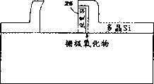
参照图9,示出了制造的器件的顶视图,其中在第二多晶硅层30上淀积光致抗蚀剂且形成图案。如图9所示,光致抗蚀剂102淀积在Si薄膜26的区域内的第二多晶硅层30上,这将形成所形成的器件的栅极。图10示出了图9的结构侧视图,其中光致抗蚀剂102在第二多晶硅层30上。Referring to FIG. 9 , a top view of the fabricated device is shown in which photoresist is deposited and patterned on the
图11示出了在使用本领域公知的蚀刻工艺,比如湿法蚀刻而蚀刻了图9的光致抗蚀剂102之后所形成的结构的顶视图。尤其是,蚀刻步骤留下将成为两个源极/漏极区域104的部分,在栅极区域106每一侧有一个。在源极/漏极区域104中,暴露出氧化物晶片10、在下面的Si薄膜26侧面和顶部上的栅极氧化物28、和第二氮化物分隔层22。在图11中Si薄膜26不可见。FIG. 11 shows a top view of the resulting structure after etching the
图12示出了图11所示器件的剖面。如图12所示,在源极/漏极区域104中进行离子注入,在栅极区域106的两侧形成延伸部分。可以使用任何适于制造器件的源极/漏极注入的离子注入工艺,如本领域所公知。此外可以使用大倾角离子注入,例如对于硼注入来说约0.2-1keV的能量级别,对于砷来说1-2keV的能量级别。FIG. 12 shows a cross-section of the device shown in FIG. 11 . As shown in FIG. 12 , ion implantation is performed in the source/
图13示出了通过在氧化物晶片10上邻近第二多晶硅层30淀积氮化物,然后蚀刻而形成氮化物分隔层108之后,所制造的器件的顶视图。图14示出了覆盖栅极氧化物28和第二氮化物分隔层22上的氮化物分隔层108。在形成氮化物分隔层108之后,在适于制造的器件的时候,可以进行其他的步骤,包括源极/漏极注入和退火。FIG. 13 shows a top view of the fabricated device after forming a
从图8所示的结构开始,图15示出了在形成应变Si双栅极翅片式FET的过程中的后续步骤,它是另一种类型的示例,其中可以实现本发明包括的应变Si薄膜。如图15所示,淀积氧化物薄膜202,且例如使用CMP(化学机械平面化)平面化。然后蚀刻掉剩余的氧化物薄膜202,使第二多晶硅层30的一部分暴露在氧化物薄膜202上方。氧化物薄膜202可以例如使用定向HDP(高密度等离子体)淀积,从而在氮化物分隔层20和22上方的区域,优先将大多数氧化物淀积在平面上,较少的氧化物淀积在多晶硅30的顶部上。Starting with the structure shown in Figure 8, Figure 15 shows the subsequent steps in the process of forming a strained Si double gate fin FET, which is an example of another type in which the strained Si film. As shown in FIG. 15, an oxide film 202 is deposited, and planarized using, for example, CMP (Chemical Mechanical Planarization). Then the remaining oxide film 202 is etched away, so that a part of the
图16示出蚀刻第二多晶硅层30的一部分,使第一和第二氮化物层20和22的一部分暴露。适当的蚀刻工艺可包括任何选择性蚀刻多晶硅的工艺,和任何选择性地蚀刻氧化物的蚀刻工艺,比如湿法蚀刻。在蚀刻之后,第一和第二氮化物分隔层20和22暴露,且伸出到第二多晶硅层30上方。第二多晶硅层30将形成第一和第二氮化物分隔层20和22、以及栅极氧化物28基底附近的突出区域。FIG. 16 shows etching a portion of the
图17示出了两个氮化物分隔层20和22的湿式选择性蚀刻和SiGe块24的湿式蚀刻结果。在整个制造工艺中,普通的蚀刻剂可以用于蚀刻氮化物,包括例如氟和氯。Si3N4至SiO2的选择性蚀刻可以利用沸腾的H3PO4溶液(例如85%H3PO4,180℃)进行,因为这种溶液腐蚀SiO2非常慢。对于Si3N4来说蚀刻速度为~10nm/min,但小于SiO2的1mm/min。Si3N4可以在浓缩的HF或缓冲的HF中在室温下蚀刻。然而,HF还蚀刻SiO2。使用反应离子等离子体蚀刻工艺,下述蚀刻化学制品可以用于Si3N4:CHF3//O2;CH2F2;CH2CHF2。通过去除SiGe块24以及第一和第二氮化物分隔层,20和22,应变Si薄膜26具有用于进一步处理的暴露侧面,比如添加另一栅极氧化物。FIG. 17 shows the results of the wet selective etching of the two
图18示出了通过栅极氧化工艺形成第二栅极氧化物208,该工艺分别在器件的暴露部分和Si薄膜26上形成薄氧化物层204。尤其是,在Si薄膜26上形成的薄氧化物层205的所述部分构成栅极氧化物205的第二栅极氧化物208部分。栅极氧化物205还包括在前面步骤中形成的第一栅极氧化物207。例如通过热氧化物生长工艺可以形成第二栅极氧化物208,从而形成高质量的氧化物。FIG. 18 shows the formation of the
而且图18示出了淀积在所述器件表面上的薄多晶硅层。然后对所述结构进行直接蚀刻,从而在薄氧化物层204一侧上形成薄多晶硅分隔层206。尤其是,薄多晶硅分隔层206邻近第二栅极氧化物208形成。多晶硅分隔层206可以避免栅极氧化物208进一步被蚀刻。薄多晶硅分隔层206可以例如约100厚。此外,形成薄多晶硅分隔层206,而使薄氧化物层204的部分暴露在第二多晶硅层30的顶部上。Also Figure 18 shows a thin layer of polysilicon deposited on the surface of the device. The structure is then etched directly, forming a thin
图19示出了对薄氧化物层204的暴露部分的蚀刻。可以使用任何选择性地蚀刻氧化物层的工艺,从而去除薄氧化物层204的暴露部分。在完成氧化物蚀刻之后,淀积多晶硅而在衬底上形成第三多晶硅层210。所形成的结构包括垂直于氧化物晶片10直立的应变Si 26翅片,在其侧面和顶部被栅极氧化物205围绕。应变Si 26的竖直翅片侧面都可以从氧化物晶片10的表面上方被接近(和触及)。而且,应变Si 26的竖直翅片包括源极/漏极区域,其两侧和顶部可以在氧化物晶片10上方被接近。FIG. 19 shows the etching of the exposed portion of the
利用本领域公知的制造步骤可以继续对图19所示的器件进行处理,从而生产完整的双栅极翅片式FET器件,该器件具有应变Si薄膜。Processing of the device shown in Figure 19 can be continued using fabrication steps known in the art to produce a complete dual gate fin FET device with strained Si film.
虽然已经根据实施例描述了本发明,但本领域的技术人员将认识到本发明可以在所附权利要求的主旨和范围内进行改进。例如,本发明可以容易地用于体式基底。While the invention has been described in terms of embodiments, those skilled in the art will recognize that the invention can be modified within the spirit and scope of the appended claims. For example, the present invention can be readily applied to body style bases.
Claims (22)
Translated fromChineseApplications Claiming Priority (2)
| Application Number | Priority Date | Filing Date | Title |
|---|---|---|---|
| US10/707,690 | 2004-01-05 | ||
| US10/707,690US7247912B2 (en) | 2004-01-05 | 2004-01-05 | Structures and methods for making strained MOSFETs |
Publications (2)
| Publication Number | Publication Date |
|---|---|
| CN1638067Atrue CN1638067A (en) | 2005-07-13 |
| CN100342507C CN100342507C (en) | 2007-10-10 |
Family
ID=34710359
Family Applications (1)
| Application Number | Title | Priority Date | Filing Date |
|---|---|---|---|
| CNB2005100042715AExpired - LifetimeCN100342507C (en) | 2004-01-05 | 2005-01-04 | Structures and methods for making strained mosfets |
Country Status (3)
| Country | Link |
|---|---|
| US (2) | US7247912B2 (en) |
| JP (1) | JP4378293B2 (en) |
| CN (1) | CN100342507C (en) |
Cited By (5)
| Publication number | Priority date | Publication date | Assignee | Title |
|---|---|---|---|---|
| WO2012000302A1 (en)* | 2010-07-01 | 2012-01-05 | 中国科学院微电子研究所 | Semiconductor device and manufacturing method thereof |
| CN103915344A (en)* | 2013-01-08 | 2014-07-09 | 中芯国际集成电路制造(上海)有限公司 | Semiconductor device and forming method thereof |
| CN104022152A (en)* | 2014-06-04 | 2014-09-03 | 重庆大学 | Double-gate p-channel MOSFET with compression strain thin film strain source and preparation method thereof |
| CN104813453A (en)* | 2012-12-20 | 2015-07-29 | 英特尔公司 | Conversion of thin transistor elements from silicon to silicon germanium |
| CN106560925A (en)* | 2015-10-05 | 2017-04-12 | 台湾积体电路制造股份有限公司 | Integrated circuit and manufacturing method thereof |
Families Citing this family (89)
| Publication number | Priority date | Publication date | Assignee | Title |
|---|---|---|---|---|
| US7410846B2 (en)* | 2003-09-09 | 2008-08-12 | International Business Machines Corporation | Method for reduced N+ diffusion in strained Si on SiGe substrate |
| US6887751B2 (en) | 2003-09-12 | 2005-05-03 | International Business Machines Corporation | MOSFET performance improvement using deformation in SOI structure |
| US7144767B2 (en)* | 2003-09-23 | 2006-12-05 | International Business Machines Corporation | NFETs using gate induced stress modulation |
| US6872641B1 (en)* | 2003-09-23 | 2005-03-29 | International Business Machines Corporation | Strained silicon on relaxed sige film with uniform misfit dislocation density |
| US7119403B2 (en)* | 2003-10-16 | 2006-10-10 | International Business Machines Corporation | High performance strained CMOS devices |
| US7303949B2 (en) | 2003-10-20 | 2007-12-04 | International Business Machines Corporation | High performance stress-enhanced MOSFETs using Si:C and SiGe epitaxial source/drain and method of manufacture |
| US7037770B2 (en)* | 2003-10-20 | 2006-05-02 | International Business Machines Corporation | Method of manufacturing strained dislocation-free channels for CMOS |
| US7129126B2 (en)* | 2003-11-05 | 2006-10-31 | International Business Machines Corporation | Method and structure for forming strained Si for CMOS devices |
| US7015082B2 (en)* | 2003-11-06 | 2006-03-21 | International Business Machines Corporation | High mobility CMOS circuits |
| US7029964B2 (en) | 2003-11-13 | 2006-04-18 | International Business Machines Corporation | Method of manufacturing a strained silicon on a SiGe on SOI substrate |
| US7122849B2 (en) | 2003-11-14 | 2006-10-17 | International Business Machines Corporation | Stressed semiconductor device structures having granular semiconductor material |
| US7247534B2 (en) | 2003-11-19 | 2007-07-24 | International Business Machines Corporation | Silicon device on Si:C-OI and SGOI and method of manufacture |
| US7049662B2 (en)* | 2003-11-26 | 2006-05-23 | International Business Machines Corporation | Structure and method to fabricate FinFET devices |
| US7198995B2 (en)* | 2003-12-12 | 2007-04-03 | International Business Machines Corporation | Strained finFETs and method of manufacture |
| US7247912B2 (en) | 2004-01-05 | 2007-07-24 | International Business Machines Corporation | Structures and methods for making strained MOSFETs |
| US7202132B2 (en) | 2004-01-16 | 2007-04-10 | International Business Machines Corporation | Protecting silicon germanium sidewall with silicon for strained silicon/silicon germanium MOSFETs |
| US7118999B2 (en)* | 2004-01-16 | 2006-10-10 | International Business Machines Corporation | Method and apparatus to increase strain effect in a transistor channel |
| US7381609B2 (en)* | 2004-01-16 | 2008-06-03 | International Business Machines Corporation | Method and structure for controlling stress in a transistor channel |
| US7205206B2 (en)* | 2004-03-03 | 2007-04-17 | International Business Machines Corporation | Method of fabricating mobility enhanced CMOS devices |
| US7223994B2 (en)* | 2004-06-03 | 2007-05-29 | International Business Machines Corporation | Strained Si on multiple materials for bulk or SOI substrates |
| TWI463526B (en)* | 2004-06-24 | 2014-12-01 | Ibm | Method for improving stress-induced CMOS components and components prepared by the method |
| US7288443B2 (en)* | 2004-06-29 | 2007-10-30 | International Business Machines Corporation | Structures and methods for manufacturing p-type MOSFET with graded embedded silicon-germanium source-drain and/or extension |
| US7384829B2 (en) | 2004-07-23 | 2008-06-10 | International Business Machines Corporation | Patterned strained semiconductor substrate and device |
| JP2006128494A (en)* | 2004-10-29 | 2006-05-18 | Toshiba Corp | Semiconductor integrated circuit device and manufacturing method thereof |
| US7393733B2 (en) | 2004-12-01 | 2008-07-01 | Amberwave Systems Corporation | Methods of forming hybrid fin field-effect transistor structures |
| US7173312B2 (en)* | 2004-12-15 | 2007-02-06 | International Business Machines Corporation | Structure and method to generate local mechanical gate stress for MOSFET channel mobility modification |
| US20060160317A1 (en)* | 2005-01-18 | 2006-07-20 | International Business Machines Corporation | Structure and method to enhance stress in a channel of cmos devices using a thin gate |
| US7256081B2 (en)* | 2005-02-01 | 2007-08-14 | International Business Machines Corporation | Structure and method to induce strain in a semiconductor device channel with stressed film under the gate |
| US7224033B2 (en) | 2005-02-15 | 2007-05-29 | International Business Machines Corporation | Structure and method for manufacturing strained FINFET |
| US7545004B2 (en)* | 2005-04-12 | 2009-06-09 | International Business Machines Corporation | Method and structure for forming strained devices |
| US8324660B2 (en) | 2005-05-17 | 2012-12-04 | Taiwan Semiconductor Manufacturing Company, Ltd. | Lattice-mismatched semiconductor structures with reduced dislocation defect densities and related methods for device fabrication |
| US9153645B2 (en) | 2005-05-17 | 2015-10-06 | Taiwan Semiconductor Manufacturing Company, Ltd. | Lattice-mismatched semiconductor structures with reduced dislocation defect densities and related methods for device fabrication |
| KR101329388B1 (en) | 2005-07-26 | 2013-11-14 | 앰버웨이브 시스템즈 코포레이션 | Solutions for integrated circuit integration of alternative active area materials |
| US7638842B2 (en) | 2005-09-07 | 2009-12-29 | Amberwave Systems Corporation | Lattice-mismatched semiconductor structures on insulators |
| US7655511B2 (en) | 2005-11-03 | 2010-02-02 | International Business Machines Corporation | Gate electrode stress control for finFET performance enhancement |
| US7564081B2 (en) | 2005-11-30 | 2009-07-21 | International Business Machines Corporation | finFET structure with multiply stressed gate electrode |
| US7635620B2 (en) | 2006-01-10 | 2009-12-22 | International Business Machines Corporation | Semiconductor device structure having enhanced performance FET device |
| US20070158743A1 (en)* | 2006-01-11 | 2007-07-12 | International Business Machines Corporation | Thin silicon single diffusion field effect transistor for enhanced drive performance with stress film liners |
| US7691698B2 (en) | 2006-02-21 | 2010-04-06 | International Business Machines Corporation | Pseudomorphic Si/SiGe/Si body device with embedded SiGe source/drain |
| WO2007112066A2 (en) | 2006-03-24 | 2007-10-04 | Amberwave Systems Corporation | Lattice-mismatched semiconductor structures and related methods for device fabrication |
| US7521307B2 (en)* | 2006-04-28 | 2009-04-21 | International Business Machines Corporation | CMOS structures and methods using self-aligned dual stressed layers |
| US7615418B2 (en)* | 2006-04-28 | 2009-11-10 | International Business Machines Corporation | High performance stress-enhance MOSFET and method of manufacture |
| US7608489B2 (en)* | 2006-04-28 | 2009-10-27 | International Business Machines Corporation | High performance stress-enhance MOSFET and method of manufacture |
| US20070281405A1 (en)* | 2006-06-02 | 2007-12-06 | International Business Machines Corporation | Methods of stressing transistor channel with replaced gate and related structures |
| US8853746B2 (en) | 2006-06-29 | 2014-10-07 | International Business Machines Corporation | CMOS devices with stressed channel regions, and methods for fabricating the same |
| US8227316B2 (en)* | 2006-06-29 | 2012-07-24 | International Business Machines Corporation | Method for manufacturing double gate finFET with asymmetric halo |
| US7790540B2 (en) | 2006-08-25 | 2010-09-07 | International Business Machines Corporation | Structure and method to use low k stress liner to reduce parasitic capacitance |
| US8754446B2 (en) | 2006-08-30 | 2014-06-17 | International Business Machines Corporation | Semiconductor structure having undercut-gate-oxide gate stack enclosed by protective barrier material |
| US7462522B2 (en)* | 2006-08-30 | 2008-12-09 | International Business Machines Corporation | Method and structure for improving device performance variation in dual stress liner technology |
| US8173551B2 (en) | 2006-09-07 | 2012-05-08 | Taiwan Semiconductor Manufacturing Co., Ltd. | Defect reduction using aspect ratio trapping |
| WO2008039495A1 (en) | 2006-09-27 | 2008-04-03 | Amberwave Systems Corporation | Tri-gate field-effect transistors formed by aspect ratio trapping |
| WO2008039534A2 (en) | 2006-09-27 | 2008-04-03 | Amberwave Systems Corporation | Quantum tunneling devices and circuits with lattice- mismatched semiconductor structures |
| US8502263B2 (en) | 2006-10-19 | 2013-08-06 | Taiwan Semiconductor Manufacturing Company, Ltd. | Light-emitter-based devices with lattice-mismatched semiconductor structures |
| US7772048B2 (en)* | 2007-02-23 | 2010-08-10 | Freescale Semiconductor, Inc. | Forming semiconductor fins using a sacrificial fin |
| US8304805B2 (en) | 2009-01-09 | 2012-11-06 | Taiwan Semiconductor Manufacturing Company, Ltd. | Semiconductor diodes fabricated by aspect ratio trapping with coalesced films |
| US8237151B2 (en) | 2009-01-09 | 2012-08-07 | Taiwan Semiconductor Manufacturing Company, Ltd. | Diode-based devices and methods for making the same |
| US7825328B2 (en) | 2007-04-09 | 2010-11-02 | Taiwan Semiconductor Manufacturing Company, Ltd. | Nitride-based multi-junction solar cell modules and methods for making the same |
| WO2008124154A2 (en) | 2007-04-09 | 2008-10-16 | Amberwave Systems Corporation | Photovoltaics on silicon |
| US8329541B2 (en) | 2007-06-15 | 2012-12-11 | Taiwan Semiconductor Manufacturing Company, Ltd. | InP-based transistor fabrication |
| US7615435B2 (en)* | 2007-07-31 | 2009-11-10 | International Business Machines Corporation | Semiconductor device and method of manufacture |
| JP2010538495A (en) | 2007-09-07 | 2010-12-09 | アンバーウェーブ・システムズ・コーポレーション | Multi-junction solar cell |
| US8115254B2 (en) | 2007-09-25 | 2012-02-14 | International Business Machines Corporation | Semiconductor-on-insulator structures including a trench containing an insulator stressor plug and method of fabricating same |
| US8492846B2 (en) | 2007-11-15 | 2013-07-23 | International Business Machines Corporation | Stress-generating shallow trench isolation structure having dual composition |
| CN101939830A (en)* | 2008-02-11 | 2011-01-05 | Nxp股份有限公司 | FinFET with discrete gates and method of manufacturing the same |
| US7967995B2 (en)* | 2008-03-31 | 2011-06-28 | Tokyo Electron Limited | Multi-layer/multi-input/multi-output (MLMIMO) models and method for using |
| US8183667B2 (en) | 2008-06-03 | 2012-05-22 | Taiwan Semiconductor Manufacturing Co., Ltd. | Epitaxial growth of crystalline material |
| US8274097B2 (en) | 2008-07-01 | 2012-09-25 | Taiwan Semiconductor Manufacturing Company, Ltd. | Reduction of edge effects from aspect ratio trapping |
| US8981427B2 (en) | 2008-07-15 | 2015-03-17 | Taiwan Semiconductor Manufacturing Company, Ltd. | Polishing of small composite semiconductor materials |
| US20100072515A1 (en) | 2008-09-19 | 2010-03-25 | Amberwave Systems Corporation | Fabrication and structures of crystalline material |
| EP2335273A4 (en) | 2008-09-19 | 2012-01-25 | Taiwan Semiconductor Mfg | FORMATION OF DEVICES BY GROWTH OF EPITAXIAL LAYERS |
| US8253211B2 (en) | 2008-09-24 | 2012-08-28 | Taiwan Semiconductor Manufacturing Company, Ltd. | Semiconductor sensor structures with reduced dislocation defect densities |
| JP2010118621A (en)* | 2008-11-14 | 2010-05-27 | Nec Electronics Corp | Semiconductor device, and method of manufacturing the same |
| US8629446B2 (en) | 2009-04-02 | 2014-01-14 | Taiwan Semiconductor Manufacturing Company, Ltd. | Devices formed from a non-polar plane of a crystalline material and method of making the same |
| US8021949B2 (en)* | 2009-12-01 | 2011-09-20 | International Business Machines Corporation | Method and structure for forming finFETs with multiple doping regions on a same chip |
| US8598006B2 (en)* | 2010-03-16 | 2013-12-03 | International Business Machines Corporation | Strain preserving ion implantation methods |
| US8796085B2 (en)* | 2012-10-12 | 2014-08-05 | Viktor Koldiaev | Vertical super-thin body semiconductor on dielectric wall devices and methods of their fabrication |
| CN103928330B (en)* | 2013-01-11 | 2017-05-24 | 中芯国际集成电路制造(上海)有限公司 | Semiconductor structure and forming method thereof |
| US8951870B2 (en)* | 2013-03-14 | 2015-02-10 | International Business Machines Corporation | Forming strained and relaxed silicon and silicon germanium fins on the same wafer |
| US9583590B2 (en) | 2013-09-27 | 2017-02-28 | Samsung Electronics Co., Ltd. | Integrated circuit devices including FinFETs and methods of forming the same |
| US9178045B2 (en) | 2013-09-27 | 2015-11-03 | Samsung Electronics Co., Ltd. | Integrated circuit devices including FinFETS and methods of forming the same |
| US9536900B2 (en) | 2014-05-22 | 2017-01-03 | Globalfoundries Inc. | Forming fins of different semiconductor materials on the same substrate |
| JP6629312B2 (en)* | 2014-07-03 | 2020-01-15 | アプライド マテリアルズ インコーポレイテッドApplied Materials,Incorporated | Method and apparatus for selective deposition |
| US9196479B1 (en) | 2014-07-03 | 2015-11-24 | International Business Machines Corporation | Method of co-integration of strained silicon and strained germanium in semiconductor devices including fin structures |
| KR102255174B1 (en) | 2014-10-10 | 2021-05-24 | 삼성전자주식회사 | Semiconductor device having active region and method of forming the same |
| US9741811B2 (en) | 2014-12-15 | 2017-08-22 | Samsung Electronics Co., Ltd. | Integrated circuit devices including source/drain extension regions and methods of forming the same |
| US9472575B2 (en) | 2015-02-06 | 2016-10-18 | International Business Machines Corporation | Formation of strained fins in a finFET device |
| KR102269415B1 (en) | 2015-03-16 | 2021-06-24 | 삼성전자주식회사 | Semiconductor device |
| US9704990B1 (en) | 2016-09-19 | 2017-07-11 | International Business Machines Corporation | Vertical FET with strained channel |
| US10600695B2 (en)* | 2018-05-22 | 2020-03-24 | International Business Machines Corporation | Channel strain formation in vertical transport FETS with dummy stressor materials |
Family Cites Families (96)
| Publication number | Priority date | Publication date | Assignee | Title |
|---|---|---|---|---|
| US3602841A (en) | 1970-06-18 | 1971-08-31 | Ibm | High frequency bulk semiconductor amplifiers and oscillators |
| US4853076A (en) | 1983-12-29 | 1989-08-01 | Massachusetts Institute Of Technology | Semiconductor thin films |
| US4665415A (en) | 1985-04-24 | 1987-05-12 | International Business Machines Corporation | Semiconductor device with hole conduction via strained lattice |
| ATE59917T1 (en) | 1985-09-13 | 1991-01-15 | Siemens Ag | CIRCUIT CONTAINING INTEGRATED BIPOLAR AND COMPLEMENTARY MOSTRANSISTORS ON A COMMON SUBSTRATE AND METHOD FOR THEIR MANUFACTURE. |
| JPS6476755A (en) | 1987-09-18 | 1989-03-22 | Hitachi Ltd | Semiconductor device |
| US4958213A (en) | 1987-12-07 | 1990-09-18 | Texas Instruments Incorporated | Method for forming a transistor base region under thick oxide |
| US5354695A (en) | 1992-04-08 | 1994-10-11 | Leedy Glenn J | Membrane dielectric isolation IC fabrication |
| US5459346A (en) | 1988-06-28 | 1995-10-17 | Ricoh Co., Ltd. | Semiconductor substrate with electrical contact in groove |
| US5006913A (en) | 1988-11-05 | 1991-04-09 | Mitsubishi Denki Kabushiki Kaisha | Stacked type semiconductor device |
| US5108843A (en) | 1988-11-30 | 1992-04-28 | Ricoh Company, Ltd. | Thin film semiconductor and process for producing the same |
| US4952524A (en) | 1989-05-05 | 1990-08-28 | At&T Bell Laboratories | Semiconductor device manufacture including trench formation |
| US5310446A (en) | 1990-01-10 | 1994-05-10 | Ricoh Company, Ltd. | Method for producing semiconductor film |
| US5060030A (en) | 1990-07-18 | 1991-10-22 | Raytheon Company | Pseudomorphic HEMT having strained compensation layer |
| US5081513A (en) | 1991-02-28 | 1992-01-14 | Xerox Corporation | Electronic device with recovery layer proximate to active layer |
| US5371399A (en) | 1991-06-14 | 1994-12-06 | International Business Machines Corporation | Compound semiconductor having metallic inclusions and devices fabricated therefrom |
| US5134085A (en) | 1991-11-21 | 1992-07-28 | Micron Technology, Inc. | Reduced-mask, split-polysilicon CMOS process, incorporating stacked-capacitor cells, for fabricating multi-megabit dynamic random access memories |
| US5391510A (en) | 1992-02-28 | 1995-02-21 | International Business Machines Corporation | Formation of self-aligned metal gate FETs using a benignant removable gate material during high temperature steps |
| US6008126A (en) | 1992-04-08 | 1999-12-28 | Elm Technology Corporation | Membrane dielectric isolation IC fabrication |
| US5561302A (en) | 1994-09-26 | 1996-10-01 | Motorola, Inc. | Enhanced mobility MOSFET device and method |
| US5670798A (en) | 1995-03-29 | 1997-09-23 | North Carolina State University | Integrated heterostructures of Group III-V nitride semiconductor materials including epitaxial ohmic contact non-nitride buffer layer and methods of fabricating same |
| US5679965A (en) | 1995-03-29 | 1997-10-21 | North Carolina State University | Integrated heterostructures of Group III-V nitride semiconductor materials including epitaxial ohmic contact, non-nitride buffer layer and methods of fabricating same |
| US5557122A (en) | 1995-05-12 | 1996-09-17 | Alliance Semiconductors Corporation | Semiconductor electrode having improved grain structure and oxide growth properties |
| KR100213196B1 (en) | 1996-03-15 | 1999-08-02 | 윤종용 | Trench device separation |
| US6403975B1 (en) | 1996-04-09 | 2002-06-11 | Max-Planck Gesellschaft Zur Forderung Der Wissenschafteneev | Semiconductor components, in particular photodetectors, light emitting diodes, optical modulators and waveguides with multilayer structures grown on silicon substrates |
| US5880040A (en) | 1996-04-15 | 1999-03-09 | Macronix International Co., Ltd. | Gate dielectric based on oxynitride grown in N2 O and annealed in NO |
| US5861651A (en) | 1997-02-28 | 1999-01-19 | Lucent Technologies Inc. | Field effect devices and capacitors with improved thin film dielectrics and method for making same |
| US5940736A (en) | 1997-03-11 | 1999-08-17 | Lucent Technologies Inc. | Method for forming a high quality ultrathin gate oxide layer |
| US6309975B1 (en) | 1997-03-14 | 2001-10-30 | Micron Technology, Inc. | Methods of making implanted structures |
| US6025280A (en) | 1997-04-28 | 2000-02-15 | Lucent Technologies Inc. | Use of SiD4 for deposition of ultra thin and controllable oxides |
| US5960297A (en) | 1997-07-02 | 1999-09-28 | Kabushiki Kaisha Toshiba | Shallow trench isolation structure and method of forming the same |
| US5981356A (en) | 1997-07-28 | 1999-11-09 | Integrated Device Technology, Inc. | Isolation trenches with protected corners |
| JP3139426B2 (en) | 1997-10-15 | 2001-02-26 | 日本電気株式会社 | Semiconductor device |
| US6066545A (en) | 1997-12-09 | 2000-05-23 | Texas Instruments Incorporated | Birdsbeak encroachment using combination of wet and dry etch for isolation nitride |
| US6274421B1 (en) | 1998-01-09 | 2001-08-14 | Sharp Laboratories Of America, Inc. | Method of making metal gate sub-micron MOS transistor |
| KR100275908B1 (en) | 1998-03-02 | 2000-12-15 | 윤종용 | Method of fabricating trench isolation in an integrated circuit |
| US6165383A (en) | 1998-04-10 | 2000-12-26 | Organic Display Technology | Useful precursors for organic electroluminescent materials and devices made from such materials |
| US6361885B1 (en) | 1998-04-10 | 2002-03-26 | Organic Display Technology | Organic electroluminescent materials and device made from such materials |
| US5989978A (en) | 1998-07-16 | 1999-11-23 | Chartered Semiconductor Manufacturing, Ltd. | Shallow trench isolation of MOSFETS with reduced corner parasitic currents |
| JP4592837B2 (en) | 1998-07-31 | 2010-12-08 | ルネサスエレクトロニクス株式会社 | Manufacturing method of semiconductor device |
| US6319794B1 (en) | 1998-10-14 | 2001-11-20 | International Business Machines Corporation | Structure and method for producing low leakage isolation devices |
| US6235598B1 (en) | 1998-11-13 | 2001-05-22 | Intel Corporation | Method of using thick first spacers to improve salicide resistance on polysilicon gates |
| US6080637A (en) | 1998-12-07 | 2000-06-27 | Taiwan Semiconductor Manufacturing Company | Shallow trench isolation technology to eliminate a kink effect |
| US6117722A (en) | 1999-02-18 | 2000-09-12 | Taiwan Semiconductor Manufacturing Company | SRAM layout for relaxing mechanical stress in shallow trench isolation technology and method of manufacture thereof |
| US6255169B1 (en) | 1999-02-22 | 2001-07-03 | Advanced Micro Devices, Inc. | Process for fabricating a high-endurance non-volatile memory device |
| US6093621A (en) | 1999-04-05 | 2000-07-25 | Vanguard International Semiconductor Corp. | Method of forming shallow trench isolation |
| US6284626B1 (en) | 1999-04-06 | 2001-09-04 | Vantis Corporation | Angled nitrogen ion implantation for minimizing mechanical stress on side walls of an isolation trench |
| DE19917365A1 (en)* | 1999-04-16 | 2000-10-19 | Patent Treuhand Ges Fuer Elektrische Gluehlampen Mbh | Method for comparing at least one operating parameter of an operating device for electric lamps |
| US6228694B1 (en) | 1999-06-28 | 2001-05-08 | Intel Corporation | Method of increasing the mobility of MOS transistors by use of localized stress regions |
| US6362082B1 (en) | 1999-06-28 | 2002-03-26 | Intel Corporation | Methodology for control of short channel effects in MOS transistors |
| US6656822B2 (en) | 1999-06-28 | 2003-12-02 | Intel Corporation | Method for reduced capacitance interconnect system using gaseous implants into the ILD |
| US6281532B1 (en) | 1999-06-28 | 2001-08-28 | Intel Corporation | Technique to obtain increased channel mobilities in NMOS transistors by gate electrode engineering |
| KR100332108B1 (en) | 1999-06-29 | 2002-04-10 | 박종섭 | Transistor in a semiconductor device and method of manufacuring the same |
| TW426940B (en) | 1999-07-30 | 2001-03-21 | United Microelectronics Corp | Manufacturing method of MOS field effect transistor |
| US6483171B1 (en) | 1999-08-13 | 2002-11-19 | Micron Technology, Inc. | Vertical sub-micron CMOS transistors on (110), (111), (311), (511), and higher order surfaces of bulk, SOI and thin film structures and method of forming same |
| US6284623B1 (en) | 1999-10-25 | 2001-09-04 | Peng-Fei Zhang | Method of fabricating semiconductor devices using shallow trench isolation with reduced narrow channel effect |
| US6476462B2 (en) | 1999-12-28 | 2002-11-05 | Texas Instruments Incorporated | MOS-type semiconductor device and method for making same |
| US6221735B1 (en) | 2000-02-15 | 2001-04-24 | Philips Semiconductors, Inc. | Method for eliminating stress induced dislocations in CMOS devices |
| US6531369B1 (en) | 2000-03-01 | 2003-03-11 | Applied Micro Circuits Corporation | Heterojunction bipolar transistor (HBT) fabrication using a selectively deposited silicon germanium (SiGe) |
| US6368931B1 (en) | 2000-03-27 | 2002-04-09 | Intel Corporation | Thin tensile layers in shallow trench isolation and method of making same |
| AU2001263211A1 (en)* | 2000-05-26 | 2001-12-11 | Amberwave Systems Corporation | Buried channel strained silicon fet using an ion implanted doped layer |
| US6940716B1 (en)* | 2000-07-13 | 2005-09-06 | Intel Corporation | Method and apparatus for dissipating heat from an electronic device |
| US6493497B1 (en) | 2000-09-26 | 2002-12-10 | Motorola, Inc. | Electro-optic structure and process for fabricating same |
| US6501121B1 (en) | 2000-11-15 | 2002-12-31 | Motorola, Inc. | Semiconductor structure |
| US7312485B2 (en) | 2000-11-29 | 2007-12-25 | Intel Corporation | CMOS fabrication process utilizing special transistor orientation |
| US6563152B2 (en) | 2000-12-29 | 2003-05-13 | Intel Corporation | Technique to obtain high mobility channels in MOS transistors by forming a strain layer on an underside of a channel |
| US20020086497A1 (en) | 2000-12-30 | 2002-07-04 | Kwok Siang Ping | Beaker shape trench with nitride pull-back for STI |
| US6265317B1 (en) | 2001-01-09 | 2001-07-24 | Taiwan Semiconductor Manufacturing Company | Top corner rounding for shallow trench isolation |
| US6458662B1 (en)* | 2001-04-04 | 2002-10-01 | Advanced Micro Devices, Inc. | Method of fabricating a semiconductor device having an asymmetrical dual-gate silicon-germanium (SiGe) channel MOSFET and a device thereby formed |
| US6403486B1 (en) | 2001-04-30 | 2002-06-11 | Taiwan Semiconductor Manufacturing Company | Method for forming a shallow trench isolation |
| US6583060B2 (en) | 2001-07-13 | 2003-06-24 | Micron Technology, Inc. | Dual depth trench isolation |
| US6531740B2 (en) | 2001-07-17 | 2003-03-11 | Motorola, Inc. | Integrated impedance matching and stability network |
| US6498358B1 (en) | 2001-07-20 | 2002-12-24 | Motorola, Inc. | Structure and method for fabricating an electro-optic system having an electrochromic diffraction grating |
| US6908810B2 (en) | 2001-08-08 | 2005-06-21 | Taiwan Semiconductor Manufacturing Co., Ltd. | Method of preventing threshold voltage of MOS transistor from being decreased by shallow trench isolation formation |
| JP2003060076A (en) | 2001-08-21 | 2003-02-28 | Nec Corp | Semiconductor device and manufacturing method thereof |
| US6831292B2 (en) | 2001-09-21 | 2004-12-14 | Amberwave Systems Corporation | Semiconductor structures employing strained material layers with defined impurity gradients and methods for fabricating same |
| US20030057184A1 (en) | 2001-09-22 | 2003-03-27 | Shiuh-Sheng Yu | Method for pull back SiN to increase rounding effect in a shallow trench isolation process |
| US6656798B2 (en) | 2001-09-28 | 2003-12-02 | Infineon Technologies, Ag | Gate processing method with reduced gate oxide corner and edge thinning |
| US6461936B1 (en) | 2002-01-04 | 2002-10-08 | Infineon Technologies Ag | Double pullback method of filling an isolation trench |
| US6800910B2 (en)* | 2002-09-30 | 2004-10-05 | Advanced Micro Devices, Inc. | FinFET device incorporating strained silicon in the channel region |
| US7388259B2 (en) | 2002-11-25 | 2008-06-17 | International Business Machines Corporation | Strained finFET CMOS device structures |
| US6825529B2 (en) | 2002-12-12 | 2004-11-30 | International Business Machines Corporation | Stress inducing spacers |
| US6717216B1 (en) | 2002-12-12 | 2004-04-06 | International Business Machines Corporation | SOI based field effect transistor having a compressive film in undercut area under the channel and a method of making the device |
| US6974981B2 (en) | 2002-12-12 | 2005-12-13 | International Business Machines Corporation | Isolation structures for imposing stress patterns |
| US6815738B2 (en)* | 2003-02-28 | 2004-11-09 | International Business Machines Corporation | Multiple gate MOSFET structure with strained Si Fin body |
| US6887798B2 (en) | 2003-05-30 | 2005-05-03 | International Business Machines Corporation | STI stress modification by nitrogen plasma treatment for improving performance in small width devices |
| US7279746B2 (en) | 2003-06-30 | 2007-10-09 | International Business Machines Corporation | High performance CMOS device structures and method of manufacture |
| US7078299B2 (en)* | 2003-09-03 | 2006-07-18 | Advanced Micro Devices, Inc. | Formation of finFET using a sidewall epitaxial layer |
| US7119403B2 (en) | 2003-10-16 | 2006-10-10 | International Business Machines Corporation | High performance strained CMOS devices |
| US8008724B2 (en) | 2003-10-30 | 2011-08-30 | International Business Machines Corporation | Structure and method to enhance both nFET and pFET performance using different kinds of stressed layers |
| US6977194B2 (en) | 2003-10-30 | 2005-12-20 | International Business Machines Corporation | Structure and method to improve channel mobility by gate electrode stress modification |
| US7015082B2 (en) | 2003-11-06 | 2006-03-21 | International Business Machines Corporation | High mobility CMOS circuits |
| US7122849B2 (en) | 2003-11-14 | 2006-10-17 | International Business Machines Corporation | Stressed semiconductor device structures having granular semiconductor material |
| US7247912B2 (en) | 2004-01-05 | 2007-07-24 | International Business Machines Corporation | Structures and methods for making strained MOSFETs |
| US7205206B2 (en) | 2004-03-03 | 2007-04-17 | International Business Machines Corporation | Method of fabricating mobility enhanced CMOS devices |
| US7504693B2 (en) | 2004-04-23 | 2009-03-17 | International Business Machines Corporation | Dislocation free stressed channels in bulk silicon and SOI CMOS devices by gate stress engineering |
| US7354806B2 (en) | 2004-09-17 | 2008-04-08 | International Business Machines Corporation | Semiconductor device structure with active regions having different surface directions and methods |
- 2004
- 2004-01-05USUS10/707,690patent/US7247912B2/ennot_activeExpired - Lifetime
- 2005
- 2005-01-04CNCNB2005100042715Apatent/CN100342507C/ennot_activeExpired - Lifetime
- 2005-01-04JPJP2005000206Apatent/JP4378293B2/ennot_activeExpired - Fee Related
- 2007
- 2007-05-29USUS11/754,627patent/US7749842B2/ennot_activeExpired - Lifetime
Cited By (12)
| Publication number | Priority date | Publication date | Assignee | Title |
|---|---|---|---|---|
| WO2012000302A1 (en)* | 2010-07-01 | 2012-01-05 | 中国科学院微电子研究所 | Semiconductor device and manufacturing method thereof |
| US8598662B2 (en) | 2010-07-01 | 2013-12-03 | Institute of Microelectronics, Chinese Academy of Sciences | Semiconductor device and method for forming the same |
| CN104813453A (en)* | 2012-12-20 | 2015-07-29 | 英特尔公司 | Conversion of thin transistor elements from silicon to silicon germanium |
| CN103915344A (en)* | 2013-01-08 | 2014-07-09 | 中芯国际集成电路制造(上海)有限公司 | Semiconductor device and forming method thereof |
| CN103915344B (en)* | 2013-01-08 | 2017-02-22 | 中芯国际集成电路制造(上海)有限公司 | Semiconductor device and forming method thereof |
| CN104022152A (en)* | 2014-06-04 | 2014-09-03 | 重庆大学 | Double-gate p-channel MOSFET with compression strain thin film strain source and preparation method thereof |
| CN106560925A (en)* | 2015-10-05 | 2017-04-12 | 台湾积体电路制造股份有限公司 | Integrated circuit and manufacturing method thereof |
| US10510753B2 (en) | 2015-10-05 | 2019-12-17 | Taiwan Semiconductor Manufacturing Co., Ltd. | Integrated circuit and manufacturing method thereof |
| CN106560925B (en)* | 2015-10-05 | 2020-01-10 | 台湾积体电路制造股份有限公司 | Integrated circuit and method of manufacturing the same |
| US11276692B2 (en) | 2015-10-05 | 2022-03-15 | Taiwan Semiconductor Manufacturing Co., Ltd. | Manufacturing method of integrated circuit |
| US11916071B2 (en) | 2015-10-05 | 2024-02-27 | Taiwan Semiconductor Manufacturing Co., Ltd. | Semiconductor device having epitaxy source/drain regions |
| US12426358B2 (en) | 2015-10-05 | 2025-09-23 | Taiwan Semiconductor Manufacturing Co., Ltd. | Semiconductor device having epitaxy source/drain regions |
Also Published As
| Publication number | Publication date |
|---|---|
| US20050145954A1 (en) | 2005-07-07 |
| CN100342507C (en) | 2007-10-10 |
| JP2005197734A (en) | 2005-07-21 |
| US7749842B2 (en) | 2010-07-06 |
| JP4378293B2 (en) | 2009-12-02 |
| US20070218620A1 (en) | 2007-09-20 |
| US7247912B2 (en) | 2007-07-24 |
Similar Documents
| Publication | Publication Date | Title |
|---|---|---|
| CN100342507C (en) | Structures and methods for making strained mosfets | |
| US7863674B2 (en) | Multiple-gate transistors formed on bulk substrates | |
| CN2704927Y (en) | Chips that can have both partially depleted and fully depleted transistors | |
| CN100345301C (en) | Integrated transistor and its manufacturing method | |
| US7172943B2 (en) | Multiple-gate transistors formed on bulk substrates | |
| US10741453B2 (en) | FinFET device | |
| CN1253943C (en) | Transistor with multiple gates and strained channel layer and method of manufacturing the same | |
| US7154118B2 (en) | Bulk non-planar transistor having strained enhanced mobility and methods of fabrication | |
| KR100674914B1 (en) | Morse transistor having a modified channel layer and method of manufacturing same | |
| US7910413B2 (en) | Structure and method of fabricating FinFET with buried channel | |
| US8648400B2 (en) | FinFET semiconductor device with germanium (GE) fins | |
| US20150162445A1 (en) | Channel strain inducing architecture and doping technique at replacement poly gate (rpg) stage | |
| JP5270094B2 (en) | Narrow body damascene tri-gate FinFET with thinned body | |
| CN1643697A (en) | Strained fin fets structure and method | |
| CN1742362A (en) | Tri-gate and gate-surround metal-oxide-semiconductor field-effect transistor device and manufacturing method thereof | |
| CN1708855A (en) | Semiconductor device with U-shaped gate structure | |
| CN1742375A (en) | Strained Trench FinFET | |
| US9679962B2 (en) | FinFET and method of manufacturing the same | |
| JP2005019970A (en) | Strained silicon fin FET device | |
| CN111370466A (en) | Field effect transistor and manufacturing method thereof | |
| CN1510756A (en) | Double gate field effect transistor and its manufacturing method | |
| CN101604705B (en) | Fin grids transistor surrounded with grid electrodes and manufacturing method thereof | |
| CN1956214A (en) | Field effect transistor and method of manufacturing the same | |
| CN110233108B (en) | A gate-around device and method of making the same | |
| CN1531103A (en) | Double gate field effect transistor and its manufacturing method |
Legal Events
| Date | Code | Title | Description |
|---|---|---|---|
| C06 | Publication | ||
| PB01 | Publication | ||
| C10 | Entry into substantive examination | ||
| SE01 | Entry into force of request for substantive examination | ||
| C14 | Grant of patent or utility model | ||
| GR01 | Patent grant | ||
| TR01 | Transfer of patent right | ||
| TR01 | Transfer of patent right | Effective date of registration:20171115 Address after:Grand Cayman, Cayman Islands Patentee after:GLOBALFOUNDRIES INC. Address before:American New York Patentee before:Core USA second LLC Effective date of registration:20171115 Address after:American New York Patentee after:Core USA second LLC Address before:American New York Patentee before:International Business Machines Corp. | |
| CX01 | Expiry of patent term | ||
| CX01 | Expiry of patent term | Granted publication date:20071010 |