CN1637488A - Liquid crystal display device and driving method thereof - Google Patents
Liquid crystal display device and driving method thereofDownload PDFInfo
- Publication number
- CN1637488A CN1637488ACNA2004101017307ACN200410101730ACN1637488ACN 1637488 ACN1637488 ACN 1637488ACN A2004101017307 ACNA2004101017307 ACN A2004101017307ACN 200410101730 ACN200410101730 ACN 200410101730ACN 1637488 ACN1637488 ACN 1637488A
- Authority
- CN
- China
- Prior art keywords
- liquid crystal
- crystal display
- voltage signal
- common
- display device
- Prior art date
- Legal status (The legal status is an assumption and is not a legal conclusion. Google has not performed a legal analysis and makes no representation as to the accuracy of the status listed.)
- Granted
Links
Images


Classifications
- G—PHYSICS
- G02—OPTICS
- G02F—OPTICAL DEVICES OR ARRANGEMENTS FOR THE CONTROL OF LIGHT BY MODIFICATION OF THE OPTICAL PROPERTIES OF THE MEDIA OF THE ELEMENTS INVOLVED THEREIN; NON-LINEAR OPTICS; FREQUENCY-CHANGING OF LIGHT; OPTICAL LOGIC ELEMENTS; OPTICAL ANALOGUE/DIGITAL CONVERTERS
- G02F1/00—Devices or arrangements for the control of the intensity, colour, phase, polarisation or direction of light arriving from an independent light source, e.g. switching, gating or modulating; Non-linear optics
- G02F1/01—Devices or arrangements for the control of the intensity, colour, phase, polarisation or direction of light arriving from an independent light source, e.g. switching, gating or modulating; Non-linear optics for the control of the intensity, phase, polarisation or colour
- G02F1/13—Devices or arrangements for the control of the intensity, colour, phase, polarisation or direction of light arriving from an independent light source, e.g. switching, gating or modulating; Non-linear optics for the control of the intensity, phase, polarisation or colour based on liquid crystals, e.g. single liquid crystal display cells
- G02F1/133—Constructional arrangements; Operation of liquid crystal cells; Circuit arrangements
- G—PHYSICS
- G09—EDUCATION; CRYPTOGRAPHY; DISPLAY; ADVERTISING; SEALS
- G09G—ARRANGEMENTS OR CIRCUITS FOR CONTROL OF INDICATING DEVICES USING STATIC MEANS TO PRESENT VARIABLE INFORMATION
- G09G3/00—Control arrangements or circuits, of interest only in connection with visual indicators other than cathode-ray tubes
- G09G3/20—Control arrangements or circuits, of interest only in connection with visual indicators other than cathode-ray tubes for presentation of an assembly of a number of characters, e.g. a page, by composing the assembly by combination of individual elements arranged in a matrix no fixed position being assigned to or needed to be assigned to the individual characters or partial characters
- G09G3/34—Control arrangements or circuits, of interest only in connection with visual indicators other than cathode-ray tubes for presentation of an assembly of a number of characters, e.g. a page, by composing the assembly by combination of individual elements arranged in a matrix no fixed position being assigned to or needed to be assigned to the individual characters or partial characters by control of light from an independent source
- G09G3/36—Control arrangements or circuits, of interest only in connection with visual indicators other than cathode-ray tubes for presentation of an assembly of a number of characters, e.g. a page, by composing the assembly by combination of individual elements arranged in a matrix no fixed position being assigned to or needed to be assigned to the individual characters or partial characters by control of light from an independent source using liquid crystals
- G09G3/3611—Control of matrices with row and column drivers
- G09G3/3648—Control of matrices with row and column drivers using an active matrix
- G09G3/3655—Details of drivers for counter electrodes, e.g. common electrodes for pixel capacitors or supplementary storage capacitors
- G—PHYSICS
- G09—EDUCATION; CRYPTOGRAPHY; DISPLAY; ADVERTISING; SEALS
- G09G—ARRANGEMENTS OR CIRCUITS FOR CONTROL OF INDICATING DEVICES USING STATIC MEANS TO PRESENT VARIABLE INFORMATION
- G09G3/00—Control arrangements or circuits, of interest only in connection with visual indicators other than cathode-ray tubes
- G09G3/20—Control arrangements or circuits, of interest only in connection with visual indicators other than cathode-ray tubes for presentation of an assembly of a number of characters, e.g. a page, by composing the assembly by combination of individual elements arranged in a matrix no fixed position being assigned to or needed to be assigned to the individual characters or partial characters
- G09G3/34—Control arrangements or circuits, of interest only in connection with visual indicators other than cathode-ray tubes for presentation of an assembly of a number of characters, e.g. a page, by composing the assembly by combination of individual elements arranged in a matrix no fixed position being assigned to or needed to be assigned to the individual characters or partial characters by control of light from an independent source
- G09G3/36—Control arrangements or circuits, of interest only in connection with visual indicators other than cathode-ray tubes for presentation of an assembly of a number of characters, e.g. a page, by composing the assembly by combination of individual elements arranged in a matrix no fixed position being assigned to or needed to be assigned to the individual characters or partial characters by control of light from an independent source using liquid crystals
- G09G3/3611—Control of matrices with row and column drivers
- G09G3/3614—Control of polarity reversal in general
- G—PHYSICS
- G09—EDUCATION; CRYPTOGRAPHY; DISPLAY; ADVERTISING; SEALS
- G09G—ARRANGEMENTS OR CIRCUITS FOR CONTROL OF INDICATING DEVICES USING STATIC MEANS TO PRESENT VARIABLE INFORMATION
- G09G3/00—Control arrangements or circuits, of interest only in connection with visual indicators other than cathode-ray tubes
- G09G3/20—Control arrangements or circuits, of interest only in connection with visual indicators other than cathode-ray tubes for presentation of an assembly of a number of characters, e.g. a page, by composing the assembly by combination of individual elements arranged in a matrix no fixed position being assigned to or needed to be assigned to the individual characters or partial characters
- G09G3/34—Control arrangements or circuits, of interest only in connection with visual indicators other than cathode-ray tubes for presentation of an assembly of a number of characters, e.g. a page, by composing the assembly by combination of individual elements arranged in a matrix no fixed position being assigned to or needed to be assigned to the individual characters or partial characters by control of light from an independent source
- G09G3/36—Control arrangements or circuits, of interest only in connection with visual indicators other than cathode-ray tubes for presentation of an assembly of a number of characters, e.g. a page, by composing the assembly by combination of individual elements arranged in a matrix no fixed position being assigned to or needed to be assigned to the individual characters or partial characters by control of light from an independent source using liquid crystals
- G09G3/3611—Control of matrices with row and column drivers
- G09G3/3648—Control of matrices with row and column drivers using an active matrix
- G—PHYSICS
- G09—EDUCATION; CRYPTOGRAPHY; DISPLAY; ADVERTISING; SEALS
- G09G—ARRANGEMENTS OR CIRCUITS FOR CONTROL OF INDICATING DEVICES USING STATIC MEANS TO PRESENT VARIABLE INFORMATION
- G09G2300/00—Aspects of the constitution of display devices
- G09G2300/04—Structural and physical details of display devices
- G09G2300/0421—Structural details of the set of electrodes
- G09G2300/0434—Flat panel display in which a field is applied parallel to the display plane
- G—PHYSICS
- G09—EDUCATION; CRYPTOGRAPHY; DISPLAY; ADVERTISING; SEALS
- G09G—ARRANGEMENTS OR CIRCUITS FOR CONTROL OF INDICATING DEVICES USING STATIC MEANS TO PRESENT VARIABLE INFORMATION
- G09G3/00—Control arrangements or circuits, of interest only in connection with visual indicators other than cathode-ray tubes
- G09G3/20—Control arrangements or circuits, of interest only in connection with visual indicators other than cathode-ray tubes for presentation of an assembly of a number of characters, e.g. a page, by composing the assembly by combination of individual elements arranged in a matrix no fixed position being assigned to or needed to be assigned to the individual characters or partial characters
- G09G3/34—Control arrangements or circuits, of interest only in connection with visual indicators other than cathode-ray tubes for presentation of an assembly of a number of characters, e.g. a page, by composing the assembly by combination of individual elements arranged in a matrix no fixed position being assigned to or needed to be assigned to the individual characters or partial characters by control of light from an independent source
- G09G3/36—Control arrangements or circuits, of interest only in connection with visual indicators other than cathode-ray tubes for presentation of an assembly of a number of characters, e.g. a page, by composing the assembly by combination of individual elements arranged in a matrix no fixed position being assigned to or needed to be assigned to the individual characters or partial characters by control of light from an independent source using liquid crystals
- G09G3/3611—Control of matrices with row and column drivers
- G09G3/3685—Details of drivers for data electrodes
- G09G3/3688—Details of drivers for data electrodes suitable for active matrices only
Landscapes
- Engineering & Computer Science (AREA)
- Physics & Mathematics (AREA)
- General Physics & Mathematics (AREA)
- Crystallography & Structural Chemistry (AREA)
- Chemical & Material Sciences (AREA)
- Computer Hardware Design (AREA)
- Theoretical Computer Science (AREA)
- Power Engineering (AREA)
- Nonlinear Science (AREA)
- Mathematical Physics (AREA)
- Optics & Photonics (AREA)
- Control Of Indicators Other Than Cathode Ray Tubes (AREA)
- Liquid Crystal (AREA)
- Liquid Crystal Display Device Control (AREA)
Abstract
Translated fromChinese
Description
Translated fromChinese技术领域technical field
本发明涉及液晶显示器,更具体地,本发明涉及一种用于降低功耗并且在基板上集成驱动器的液晶显示器件及其制造方法。The present invention relates to a liquid crystal display, and more particularly, to a liquid crystal display device for reducing power consumption and integrating a driver on a substrate and a manufacturing method thereof.
背景技术Background technique
通常,液晶显示器(LCD)采用电场来控制液晶的透光率,以显示图像。根据液晶的电场驱动方向,可以将液晶显示器大致分类为垂直电场型和水平电场型。Generally, a liquid crystal display (LCD) uses an electric field to control light transmittance of liquid crystals to display images. Liquid crystal displays can be roughly classified into a vertical electric field type and a horizontal electric field type according to the electric field driving direction of the liquid crystal.
垂直电场施加型液晶显示器采用在上基板和下基板上彼此相对设置的像素电极和公共电极之间形成的垂直电场以扭曲向列(TN)模式来驱动液晶。垂直电场施加型的液晶显示器具有大孔径比的优点,同时具有大约90°的窄视角的缺点。A vertical electric field application type liquid crystal display drives liquid crystals in a twisted nematic (TN) mode using a vertical electric field formed between a pixel electrode and a common electrode disposed opposite to each other on upper and lower substrates. A liquid crystal display of a vertical electric field application type has an advantage of a large aperture ratio while having a disadvantage of a narrow viewing angle of about 90°.
水平电场施加型液晶显示器采用在下基板上彼此平行设置的像素电极和公共电极之间形成的水平电场以面内切换(IPS)模式来驱动液晶。水平电场施加型的液晶显示器具有大约160°的宽视角的优点。The horizontal electric field application type liquid crystal display drives liquid crystals in an in-plane switching (IPS) mode using a horizontal electric field formed between pixel electrodes and a common electrode disposed parallel to each other on a lower substrate. A liquid crystal display of a horizontal electric field application type has an advantage of a wide viewing angle of about 160°.
下文中,将详细说明水平电场施加型液晶显示器。Hereinafter, a horizontal electric field application type liquid crystal display will be described in detail.
图1是表示现有技术的水平电场施加型液晶显示器的结构的方框图。FIG. 1 is a block diagram showing the structure of a conventional horizontal electric field application type liquid crystal display.
在图1中,现有技术的水平电场施加型液晶显示器包括:液晶显示板10;用于驱动液晶显示板10的数据线DL的数据驱动器2;用于驱动液晶显示板10的选通线GL的选通驱动器4;用于控制选通驱动器4和数据驱动器2的定时控制器6;以及用于将基准电压信号施加给液晶显示板10的公共线CL的公共电压发生器8。In FIG. 1 , the prior art horizontal electric field application type liquid crystal display includes: a liquid crystal display panel 10; a
定时控制器6将从其外部输入的像素数据信号R、G和B数据施加给数据驱动器2。此外,定时控制器6响应于从其外部输入的控制信号H、V、DE和CLK,分别产生用于驱动选通驱动器4和数据驱动器2的选通控制信号GDC和数据控制信号DDC。The timing controller 6 applies pixel data signals R, G, and B data input from the outside thereof to the
选通控制信号GDC例如包括选通启动脉冲GSP、选通移位时钟(shiftclock)GSC和选通输出使能信号GOE等。数据控制信号DDC例如包括源启动脉冲SSP、源移位时钟信号SSC、源输出使能信号SOE和极性控制信号POL等。The gate control signal GDC includes, for example, a gate start pulse GSP, a gate shift clock (GSC) GSC, a gate output enable signal GOE, and the like. The data control signal DDC includes, for example, a source start pulse SSP, a source shift clock signal SSC, a source output enable signal SOE, a polarity control signal POL, and the like.
选通驱动器4响应于来自定时控制器6的选通控制信号GDC,将扫描脉冲依次施加给选通线GL1到GLn。因此,选通驱动器4使得对于每一条选通线GL能够将薄膜晶体管TFT连接到要进行驱动的选通线GL1到GLn。The gate driver 4 sequentially applies scan pulses to the gate lines GL1 to GLn in response to the gate control signal GDC from the timing controller 6 . Therefore, the gate driver 4 enables the connection of the thin film transistor TFT to the gate lines GL1 to GLn to be driven for each gate line GL.
数据驱动器2响应于来自定时控制器6的数据控制信号DDC的每一个水平周期H1、H2、...,将每一个水平行的像素电压信号施加给数据线DL1到DLm。具体地,数据驱动器2采用来自咖马电压发生器(未示出)的咖马电压,将来自定时控制器6的数字像素数据R、G和B转换为模拟电压信号。The
公共电压发生器8产生公共电压Vcom并通过公共线CL将公共电压Vcom施加给公共电极,以形成沿像素电极的水平电场。The common voltage generator 8 generates a common voltage Vcom and applies the common voltage Vcom to the common electrode through the common line CL to form a horizontal electric field along the pixel electrode.
液晶显示板10包括设置在n条选通线GL1到GLn和m条数据线DL1到DLm之间的各个交叉点处的薄膜晶体管TFT,以及连接到薄膜晶体管TFT并以矩阵形式设置的液晶单元Clc。The liquid crystal display panel 10 includes thin film transistors TFT disposed at respective intersections between n gate lines GL1 to GLn and m data lines DL1 to DLm, and liquid crystal cells Clc connected to the thin film transistors TFT and arranged in a matrix form. .
薄膜晶体管TFT根据来自选通线GL1到GLn的选通信号将来自数据线DL1到DLm的数据施加给液晶单元Clc。如图2所示,由于液晶单元包括与薄膜晶体管TFT相连的像素电极12,以及平行于像素电极12设置以形成水平电场并与公共线CL相连的公共电极14,所以可以将其等效地表示为液晶电容器Clc。这种液晶单元包括由彼此重叠并具有至少一层绝缘膜的公共线CL和像素电极12组成的存储电容器Cst,以保持充入液晶电容器Clc中的像素电压信号,直到其中充入下一像素电压信号为止。The thin film transistors TFT apply data from the data lines DL1 to DLm to the liquid crystal cells Clc according to gate signals from the gate lines GL1 to GLn. As shown in Figure 2, since the liquid crystal cell includes a pixel electrode 12 connected to the thin film transistor TFT, and a common electrode 14 arranged parallel to the pixel electrode 12 to form a horizontal electric field and connected to the common line CL, it can be equivalently represented is the liquid crystal capacitor Clc. This liquid crystal cell includes a storage capacitor Cst consisting of a common line CL and a pixel electrode 12 overlapping each other and having at least one insulating film, to hold a pixel voltage signal charged in the liquid crystal capacitor Clc until the next pixel voltage is charged therein. until the signal.
在这种LCD中,采用驱动系统(例如行倒相(inversion)、列倒相和点倒相)来驱动液晶显示板上的液晶单元。In such an LCD, a driving system such as row inversion, column inversion, and dot inversion is used to drive liquid crystal cells on a liquid crystal display panel.
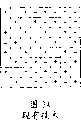
如图3A和图3B中所示,点倒相驱动系统使得能够将具有与在水平方向和垂直方向彼此相邻的其它液晶单元相反极性的像素电压信号施加给液晶单元,并且使得对于每一帧能够将像素电压信号的极性反转。点倒相驱动系统消除了在水平方向和垂直方向上相对于彼此相邻的液晶单元之间产生的串扰,由此提供比其它倒相系统更好的图像质量。As shown in FIG. 3A and FIG. 3B , the dot inversion driving system makes it possible to apply to the liquid crystal cell a pixel voltage signal having a polarity opposite to that of other liquid crystal cells adjacent to each other in the horizontal direction and the vertical direction, and makes it possible for each The frame is capable of inverting the polarity of the pixel voltage signal. The dot inversion drive system eliminates crosstalk generated between liquid crystal cells adjacent to each other in the horizontal and vertical directions, thereby providing better image quality than other inversion systems.
在由这种点倒相驱动系统驱动的图1和图2中所示的液晶单元中,对于每一个垂直周期1V以交流的形式交替地施加正(+)和负(-)像素电压信号Vd,同时如图4中所示,以直流的形式施加提供给公共线CL的公共电压信号Vcom。因此,施加给像素电极12的像素电压信号Vd和施加给公共电极14的公共电压信号Vcom具有彼此相对低电平的所需电压差ΔV。因此,为了将液晶的配向改变为所需的角度,需要具有基于公共电压信号Vcom的相对高电平的像素电压信号Vd。这种要求产生了下述问题:用于产生像素电压信号Vd的数据驱动器具有相对高的成本。In the liquid crystal cells shown in Figures 1 and 2 driven by this dot inversion drive system, positive (+) and negative (-) pixel voltage signals Vd are alternately applied in the form of alternating current for each
此外,由像素电压信号Vd和公共电压信号Vcom之间的电压差形成的水平电场在像素电极12和公共电极14之间的距离变得较近时比在这两个电极12和14之间的距离变得较远时更大。因此,即使在像素电极12和公共电极14彼此靠近时施加给像素电极12的像素电压信号Vd低于在它们彼此远离时施加给像素电极12的像素电压信号Vd,也可以获得所需的水平电场。然而,会产生下述问题:随着这两个电极12和14之间的距离变得较近,透光区域变窄,由此使孔径比降低。另一方面,会产生下述问题:如果将两个电极12和14之间的距离变得较远以提高孔径比,则施加给像素电极12的像素电压信号Vd的输出值变高,由此增加数据驱动器2的成本。In addition, the horizontal electric field formed by the voltage difference between the pixel voltage signal Vd and the common voltage signal Vcom is larger than that between the two electrodes 12 and 14 when the distance between the pixel electrode 12 and the common electrode 14 becomes closer. Larger as the distance becomes longer. Therefore, even if the pixel voltage signal Vd applied to the pixel electrode 12 when the pixel electrode 12 and the common electrode 14 are close to each other is lower than the pixel voltage signal Vd applied to the pixel electrode 12 when they are far away from each other, a desired horizontal electric field can be obtained. . However, there arises a problem that as the distance between these two electrodes 12 and 14 becomes closer, the light-transmitting area becomes narrower, thereby reducing the aperture ratio. On the other hand, there is a problem that if the distance between the two electrodes 12 and 14 is made larger to increase the aperture ratio, the output value of the pixel voltage signal Vd applied to the pixel electrode 12 becomes high, whereby Increase the cost of
在现有技术的LCD中,将选通驱动器4和数据驱动器2分离为要制造成芯片形状的多个集成电路(IC)。通过膜上芯片(COF)系统将各个驱动IC安装到在带载封装(TCP)上开出的IC区域上,或者安装在TCP的基底膜(base film)上,并通过带自动键合(TAB)系统将各个驱动IC电连接到液晶显示板10。In the related art LCD, the gate driver 4 and the
通过柔性印刷电路(FPC)和子印刷电路板(PCB),将通过TCP安装到液晶显示板10上的驱动IC连接到定时控制器和主PCB的电源。更具体地,数据驱动IC从通过FPC和数据PCB安装到主PCB上的定时控制器接收数据控制信号和像素数据,以及来自电源的功率信号(powersignal)。选通驱动IC从通过选通FPC和选通PCB安装到主PCB上的定时控制器接收选通控制信号,以及来自电源的功率信号。The driving IC mounted on the liquid crystal display panel 10 through TCP is connected to a timing controller and a power supply of the main PCB through a flexible printed circuit (FPC) and a sub printed circuit board (PCB). More specifically, the data driving IC receives a data control signal and pixel data from a timing controller mounted on a main PCB through an FPC and a data PCB, and a power signal from a power source. The gate driving IC receives a gate control signal from a timing controller mounted on a main PCB through a gate FPC and a gate PCB, and a power signal from a power source.
如上所述,选通驱动器4和数据驱动器2中的每一个都需要单独的驱动IC、TCP、PCB和FPC等。现有技术的LCD具有下述问题:由于这些单独的元件所占用的重量,使得难以具有薄的设计。As described above, each of the gate driver 4 and the
发明内容Contents of the invention
因此,本发明致力于一种液晶显示器件及其驱动方法。Accordingly, the present invention is directed to a liquid crystal display device and a driving method thereof.
本发明的优点是提供了一种用于降低功耗以及在基板上集成驱动器的液晶显示器件及其制造方法。The advantage of the present invention is to provide a liquid crystal display device for reducing power consumption and integrating a driver on a substrate and a manufacturing method thereof.
为了实现本发明的这些和其它优点,根据本发明一个方面的液晶显示器件包括:液晶显示板,该液晶显示板具有设置在基板上的多条选通线和多条数据线之间的交叉点处并基于该多条选通线以z形图案(zigzagpattern)连接的多个薄膜晶体管、与该多个薄膜晶体管相连的多个像素电极、用于与该多个像素电极一起形成水平电场的多个公共电极、以及与该多个公共电极相连并与该多条选通线基本平行设置的多条公共线;选通驱动器,用于将扫描脉冲信号施加给液晶显示板的该多条选通线;数据驱动器,用于将像素电压信号施加给液晶显示板的该多条数据线;以及公共驱动器,用于将交流公共电压信号施加给液晶显示板的该多条公共线,其中在基板上集成该选通驱动器和公共驱动器。In order to achieve these and other advantages of the present invention, a liquid crystal display device according to an aspect of the present invention includes: a liquid crystal display panel having intersections between a plurality of gate lines and a plurality of data lines disposed on a substrate A plurality of thin film transistors connected in a zigzag pattern based on the plurality of gate lines, a plurality of pixel electrodes connected to the plurality of thin film transistors, and a plurality of thin film transistors for forming a horizontal electric field together with the plurality of pixel electrodes a plurality of common electrodes connected to the plurality of common electrodes and arranged substantially in parallel with the plurality of gate lines; a gate driver for applying scan pulse signals to the plurality of gate lines of the liquid crystal display panel line; a data driver, which is used to apply pixel voltage signals to the multiple data lines of the liquid crystal display panel; and a common driver, which is used to apply an AC common voltage signal to the multiple common lines of the liquid crystal display panel, wherein on the substrate Integrates the strobe driver and the common driver.
一种驱动液晶显示器件的方法,该液晶显示器件具有:液晶显示板,该液晶显示板包括设置在基板上的多条选通线和多条数据线之间的交叉点处并基于该多条选通线以z形图案连接的多个薄膜晶体管、与该多个薄膜晶体管相连的多个像素电极、用于与该多个像素电极一起形成水平电场的多个公共电极、以及与该多个公共电极相连并与该多条选通线基本平行设置的多条公共线;以及集成在液晶显示板的基板上的公共驱动器和选通驱动器,用于分别驱动该多条公共线和该多条选通线,该方法包括:将扫描脉冲信号施加给该多条选通线;将像素电压信号施加给该多条数据线;以及将交流公共电压信号施加给液晶显示板的该多条公共线。A method for driving a liquid crystal display device, the liquid crystal display device has: a liquid crystal display panel, the liquid crystal display panel includes a plurality of gate lines and a plurality of data lines arranged on the substrate at intersections and based on the plurality of A plurality of thin film transistors connected by gate lines in a zigzag pattern, a plurality of pixel electrodes connected to the plurality of thin film transistors, a plurality of common electrodes for forming a horizontal electric field with the plurality of pixel electrodes, and a plurality of common electrodes connected with the plurality of pixel electrodes. A plurality of common lines connected to the common electrodes and substantially parallel to the plurality of gate lines; and a common driver and a gate driver integrated on the substrate of the liquid crystal display panel, used to respectively drive the plurality of common lines and the plurality of A gate line, the method includes: applying a scan pulse signal to the multiple gate lines; applying a pixel voltage signal to the multiple data lines; and applying an AC common voltage signal to the multiple common lines of the liquid crystal display panel .
附图说明Description of drawings
附图说明了本发明的实施例并与说明书一起用于说明本发明的原理,包含附图以提供对本发明的进一步理解,并且将其并入并构成说明书的一部分。The accompanying drawings illustrate embodiments of the invention and together with the description serve to explain the principles of the invention, are included to provide a further understanding of the invention, and are incorporated in and constitute a part of this specification.
在附图中:In the attached picture:
图1是表示现有技术的水平电场施加型液晶显示器的结构的示意性方框图;1 is a schematic block diagram showing the structure of a prior art horizontal electric field application type liquid crystal display;
图2是图1中所示的液晶显示板的详细平面图;Fig. 2 is a detailed plan view of the liquid crystal display panel shown in Fig. 1;
图3A和图3B是表示驱动图1中所示液晶显示器的方法中的点倒相系统的视图;3A and 3B are views representing a dot inversion system in a method of driving a liquid crystal display shown in FIG. 1;
图4是施加给图2中所示的液晶单元的像素电压信号和公共电压信号的波形图;Fig. 4 is a waveform diagram of a pixel voltage signal and a common voltage signal applied to the liquid crystal unit shown in Fig. 2;
图5是表示根据本发明第一实施例的液晶显示器的结构的示意性方框图;5 is a schematic block diagram showing the structure of a liquid crystal display according to a first embodiment of the present invention;
图6A和图6B分别是图5中所示的液晶显示板的详细平面图和详细剖面图;6A and 6B are respectively a detailed plan view and a detailed sectional view of the liquid crystal display panel shown in FIG. 5;
图7A和图7B表示由点倒相系统在奇数帧和偶数帧施加给图5中所示的液晶单元的像素电压信号的极性;7A and 7B represent the polarity of the pixel voltage signal applied to the liquid crystal cell shown in FIG. 5 in odd frames and even frames by the dot inversion system;
图8是图5中所示的选通驱动器的详细方框图;Figure 8 is a detailed block diagram of the gate driver shown in Figure 5;
图9是由图8中所示的选通驱动器产生的扫描脉冲的波形图;Fig. 9 is the waveform diagram of the scan pulse generated by the gate driver shown in Fig. 8;
图10是图5中所示的公共驱动器的详细方框图;Figure 10 is a detailed block diagram of the common driver shown in Figure 5;
图11是由图10中所示的公共驱动器产生的公共电压信号的波形图;FIG. 11 is a waveform diagram of a common voltage signal generated by a common driver shown in FIG. 10;
图12A和图12B是表示图11中所示的各种形状的公共电压信号的波形图;12A and FIG. 12B are waveform diagrams representing common voltage signals of various shapes shown in FIG. 11;
图13是施加给图5中所示的液晶单元的像素电压信号和公共电压信号的波形图;Fig. 13 is a waveform diagram of a pixel voltage signal and a common voltage signal applied to the liquid crystal unit shown in Fig. 5;
图14是表示根据本发明第二实施例的液晶显示器的结构的示意性方框图;14 is a schematic block diagram showing the structure of a liquid crystal display according to a second embodiment of the present invention;
图15是表示根据本发明第三实施例的液晶显示器的结构的示意性方框图。FIG. 15 is a schematic block diagram showing the structure of a liquid crystal display according to a third embodiment of the present invention.
具体实施方式Detailed ways
现将详细说明本发明的实施例,其示例在附图中示出。Reference will now be made in detail to embodiments of the invention, examples of which are illustrated in the accompanying drawings.
下文中,将参照图5到15详细地说明本发明的实施例。Hereinafter, an embodiment of the present invention will be described in detail with reference to FIGS. 5 to 15 .
图5表示根据本发明第一实施例的水平电场施加型液晶显示器(LCD)。FIG. 5 shows a horizontal electric field application type liquid crystal display (LCD) according to a first embodiment of the present invention.
在图5中,该水平电场施加型LCD包括:液晶显示板110;用于驱动液晶显示板110的多条数据线DL的数据驱动器102;与用于驱动液晶显示板110的多条选通线GL的选通驱动器104和用于驱动液晶显示板110的多条公共线CL的公共驱动器108集成设置的信号驱动器120;以及用于控制信号驱动器120和数据驱动器102的定时控制器106。In FIG. 5, the horizontal electric field application type LCD includes: a liquid
液晶显示板110包括:多条选通线GL;在绝缘的基础上与该多条选通线GL交叉的数据线DL。对由多条选通线GL和多条数据线DL之间的交叉点限定的各个区域设置液晶单元。如图6A和图6B中所示,每一个液晶单元包括:与多条选通线GL中的任何一条和多条数据线DL中的任何一条相连的薄膜晶体管TFT;以及由连接到薄膜晶体管TFT的像素电极112和与像素电极112基本平行设置以形成水平电场并连接到公共线CL的公共电极114组成的液晶电容器Clc。每一个液晶单元还包括存储电容器Cst,用于保持充入液晶电容器Clc中的数据电压,直到其中充入下一数据电压为止。这里,可以由保护膜118上的透明导电材料形成像素电极112和公共电极114。通过暴露薄膜晶体管TFT的漏极的接触孔,将像素电极112电连接到漏极,而通过穿过栅绝缘膜116和保护膜118的接触孔,将公共电极114电连接到以矩形脉冲形状形成的公共线CL。The liquid
薄膜晶体管TFT响应于扫描信号(即,来自对应选通线GL的选通信号)将来自对应数据线DL的像素电压信号施加给液晶单元。The thin film transistor TFT applies a pixel voltage signal from a corresponding data line DL to the liquid crystal cell in response to a scan signal (ie, a gate signal from a corresponding gate line GL).
具体地,可以沿选通线GL以z形图案连接薄膜晶体管TFT。因此,由选通线GL驱动的液晶单元基于对应选通线GL以z形图案进行设置。换句话说,对于每一列由不同的选通线GL交替地驱动在相同水平行上构成的液晶单元。因此,无论何时驱动每一条选通线GL,都可以驱动在两个相邻水平行处以z形图案设置的液晶单元,从而通过两条选通线GL来驱动每一个水平行。Specifically, the thin film transistors TFT may be connected in a zigzag pattern along the gate line GL. Accordingly, the liquid crystal cells driven by the gate lines GL are arranged in a zigzag pattern based on the corresponding gate lines GL. In other words, the liquid crystal cells formed on the same horizontal row are alternately driven by different gate lines GL for each column. Therefore, whenever each gate line GL is driven, the liquid crystal cells arranged in a zigzag pattern at two adjacent horizontal rows may be driven, thereby driving each horizontal row through the two gate lines GL.
更具体地,通过薄膜晶体管TFT连接到奇数数据线DL1、DL3、...、DLm-1的奇数列处的液晶单元由位于该液晶单元下端的彼此相邻的选通线GL2到GLn来驱动。另一方面,通过薄膜晶体管TFT连接到偶数数据线DL2、DL4、...、DLm的偶数列处的液晶单元由位于该液晶单元上端的彼此相邻的选通线GL1到GLn-1来驱动。换句话说,由第(i+1)选通线GLi+1来驱动第i水平行的液晶单元中位于奇数列处的液晶单元,而由第i选通线GLi来驱动位于偶数列处的液晶单元。More specifically, liquid crystal cells at odd columns connected to odd data lines DL1, DL3, . . On the other hand, liquid crystal cells at even columns connected to even data lines DL2, DL4, . . In other words, the (i+1)th gate line GLi+1 drives the liquid crystal cells located in the odd-numbered columns of the i-th horizontal row of liquid crystal cells, and the i-th gate line GLi drives the liquid crystal cells located in the even-numbered columns. LCD unit.
例如,由第二选通线GL2来驱动第一水平行的液晶单元中位于奇数列处的液晶单元,而由第一选通线GL1来驱动位于偶数列处的液晶单元。类似地,通过第n选通线GLn来驱动第n水平行的液晶单元中位于奇数列处的液晶单元,而通过第(n-1)选通线GL(n-1)来驱动位于偶数列处的液晶单元。另一方面,由第一选通线GL1来驱动第一水平行的液晶单元中位于奇数列处的液晶单元,而通过第二选通线GL2来驱动位于偶数列处的液晶单元。类似地,通过第(n-1)选通线GL(n-1)来驱动第n条水平行的液晶单元中位于奇数列处的液晶单元,而通过第n选通线GLn来驱动位于偶数列处的液晶单元。For example, liquid crystal cells located in odd columns among the liquid crystal cells in the first horizontal row are driven by the second gate line GL2 , and liquid crystal cells located in even columns are driven by the first gate line GL1 . Similarly, the nth gate line GLn is used to drive the liquid crystal cells located in the odd-numbered columns of the nth horizontal row of liquid crystal cells, and the (n-1)th gate line GL(n-1) is used to drive the liquid crystal cells located in the even-numbered columns the liquid crystal unit. On the other hand, liquid crystal cells located in odd columns among the liquid crystal cells in the first horizontal row are driven by the first gate line GL1 , and liquid crystal cells located in even columns are driven by the second gate line GL2 . Similarly, the liquid crystal cells located in the odd-numbered columns of the liquid crystal cells in the nth horizontal row are driven by the (n-1)th gate line GL(n-1), and the liquid crystal cells located in the even-numbered columns are driven by the nth gate line GLn. LCD cells at the column.
如上所述,无论何时驱动各条选通线GL1到GLn,都可以驱动在两个相邻水平行处以z形图案设置的液晶单元,因此,当由点倒相系统在液晶单元中充入像素电压信号时,由水平行倒相系统来驱动液晶显示板110。As described above, whenever the respective gate lines GL1 to GLn are driven, the liquid crystal cells arranged in a zigzag pattern at two adjacent horizontal rows can be driven, so when the liquid crystal cells are filled in by the dot inversion system When the pixel voltage signal is used, the liquid
例如,在图7A中所示的一个帧的时间间隔内,当驱动第一选通线GL1时,在第一水平行的偶数液晶单元中充入负(-)像素电压信号。接下来,当驱动第二选通线GL2时,在第一水平行的奇数液晶单元中充入负(-)像素电压信号,而在第二水平线的偶数液晶单元中充入正(+)像素电压信号。当驱动第三选通线GL3时,在第二水平行的奇数液晶单元中充入正(+)像素电压信号,而在第三水平行的偶数液晶单元中充入负(-)像素电压信号。因此,在第一水平行的液晶单元中充入负(-)像素电压信号,而在第二水平行的液晶单元中充入正(+)像素电压信号。结果,由水平行倒相系统驱动液晶显示板110。For example, during a time interval of one frame shown in FIG. 7A, when the first gate line GL1 is driven, negative (-) pixel voltage signals are charged in the even liquid crystal cells of the first horizontal row. Next, when the second gate line GL2 is driven, negative (-) pixel voltage signals are charged in the odd-numbered liquid crystal cells of the first horizontal line, and positive (+) pixels are charged in the even-numbered liquid crystal cells of the second horizontal line voltage signal. When the third gate line GL3 is driven, a positive (+) pixel voltage signal is charged in the odd-numbered liquid crystal cells of the second horizontal row, and a negative (-) pixel voltage signal is charged in the even-numbered liquid crystal cells of the third horizontal row . Therefore, negative (-) pixel voltage signals are charged in the liquid crystal cells of the first horizontal row, and positive (+) pixel voltage signals are charged in the liquid crystal cells of the second horizontal row. As a result, the liquid
在图7B中所示的下一个帧时间间隔内,当驱动第一选通线GL1时,在第一水平行的偶数液晶单元中充入正(+)像素电压信号。接下来,当驱动第二选通线GL2时,在第一水平行的奇数液晶单元中充入正(+)的像素电压信号,而在第二水平行的偶数液晶单元中充入负(-)像素电压信号。当驱动第三选通线GL3时,在第二水平行的奇数液晶单元中充入负(-)像素电压信号,而在第三水平行的偶数液晶单元中充入正(+)像素电压信号。因此,在第一水平行的液晶单元中充入正(+)像素电压信号,而在第二水平行的液晶单元中充入负(-)像素电压信号。结果,由水平行倒相系统来驱动液晶显示板110。In the next frame time interval shown in FIG. 7B, when the first gate line GL1 is driven, the even-numbered liquid crystal cells in the first horizontal row are charged with a positive (+) pixel voltage signal. Next, when the second gate line GL2 is driven, a positive (+) pixel voltage signal is charged in the odd-numbered liquid crystal cells of the first horizontal row, and a negative (-) pixel voltage signal is charged in the even-numbered liquid crystal cells of the second horizontal row. ) pixel voltage signal. When the third gate line GL3 is driven, negative (-) pixel voltage signals are charged in the odd-numbered liquid crystal cells of the second horizontal row, and positive (+) pixel voltage signals are charged in the even-numbered liquid crystal cells of the third horizontal row . Therefore, a positive (+) pixel voltage signal is charged in the liquid crystal cells of the first horizontal row, and a negative (−) pixel voltage signal is charged in the liquid crystal cells of the second horizontal row. As a result, the liquid
定时控制器16将从其外部输入的像素数据信号R、G和B数据提供给数据驱动器102。此外,定时控制器16响应于从其外部输入的控制信号H、V、DE和CLK,产生用于分别驱动数据驱动器102、包含在信号线驱动器120中的选通驱动器104和公共驱动器108的数据控制信号DDC、选通控制信号GDC和公共控制信号CDC。The timing controller 16 supplies pixel data signals R, G, and B data input from the outside thereof to the
选通控制信号GDC例如包括选通启动脉冲GSP、选通移位时钟GSC和选通输出使能信号GOE等。数据控制信号DDC例如包括源启动脉冲SSP、源移位时钟信号SSC、源输出使能信号SOE和极性控制信号POL等。公共控制信号CDC包括公共启动脉冲CSP和公共转换时钟信号CSC等。The gate control signal GDC includes, for example, a gate start pulse GSP, a gate shift clock GSC, a gate output enable signal GOE, and the like. The data control signal DDC includes, for example, a source start pulse SSP, a source shift clock signal SSC, a source output enable signal SOE, a polarity control signal POL, and the like. The common control signal CDC includes a common start pulse CSP, a common switching clock signal CSC, and the like.
数据驱动器102响应于来自定时控制器106的数据控制信号DDC,在每一个水平周期H1、H2、...将各个水平行的像素信号施加给数据线DL1到DLm。具体地,数据驱动器102使用来自咖马电压发生器(未示出)的咖马电压将来自定时控制器106的数字像素数据R、G和B转换为模拟像素信号。数据驱动器102使用点倒相系统施加像素电压信号,以使得对于各个水平行时间间隔和各个垂直行时间间隔,像素电压信号的极性不同。The
通过在液晶显示板110的基板101上集成用于驱动选通线GL的选通驱动器104和用于驱动公共线CL的公共驱动器108来设置信号驱动器120。为此,通过与在液晶显示板110的显示区域形成的薄膜晶体管TFT相同的工艺,同时设置包括在信号驱动器120中的选通驱动器104和公共驱动器108。设置在信号驱动器120中的薄膜晶体管TFT可以由具有高电荷迁移率的多晶硅薄膜晶体管或非晶硅薄膜晶体管制成。例如,可以通过使用低温多晶硅薄膜晶体管的CMOS工艺,在基板101上集成选通驱动器104和公共驱动器108。如图5中所示,将信号驱动器120的输出线设置为使得连接到选通线GL的选通输出线和连接到公共线CL的公共输出线交替设置。The
嵌入在信号驱动器120中的选通驱动器104响应于来自定时控制器106的选通控制信号GDC,将扫描信号依次施加给选通线GL1到GLn。因此,选通驱动器104使得对于每一条选通线GL能够驱动连接到选通线GL1到GLn的薄膜晶体管TFT。The
为此,如图8中所示,选通驱动器104包括:移位寄存器132,用于依次产生扫描信号;电平转换器(level shifter)134,用于以适合于驱动液晶单元Clc的方式来转换扫描信号的电压的摆幅宽度;以及缓冲器136,连接在电平转换器134和选通线GL之间,以用作为电压跟随器。For this reason, as shown in Figure 8,
下文中,将结合图9来对选通驱动器104的各个元件进行说明。Hereinafter, each element of the
移位寄存器132响应于图9中所示的选通移位时钟信号GSC对选通启动脉冲GSP进行移位,由此依次使选通线GL使能。当完成一个帧的选通线GL的使能操作时,移位寄存器132在发送进位值之后在下一帧重复选通线GL的使能操作。The shift register 132 shifts the gate start pulse GSP in response to the gate shift clock signal GSC shown in FIG. 9 , thereby sequentially enabling the gate lines GL. When the enable operation of the gate line GL for one frame is completed, the shift register 132 repeats the enable operation of the gate line GL in the next frame after transmitting the carry value.
电平转换器134将对要施加给选通线GL的扫描脉冲依次进行电平转换,以将它们输出给缓冲器136。换句话说,当选通移位时钟信号GSC具有高逻辑时,电平转换器134响应于选通使能信号GOE将高逻辑的扫描脉冲VGH施加给缓冲器136,而当选通移位时钟信号GSC具有低逻辑时,响应于选通使能信号GOE将低逻辑的扫描脉冲VGL施加给缓冲器136。The level shifter 134 will sequentially level shift the scan pulses to be applied to the gate lines GL to output them to the buffer 136 . In other words, when the gate shift clock signal GSC has a high logic, the level shifter 134 applies a high logic scan pulse VGH to the buffer 136 in response to the gate enable signal GOE, and when the gate shift clock signal GSC When having a low logic, a scan pulse VGL of a low logic is applied to the buffer 136 in response to the gate enable signal GOE.
缓冲器136产生具有与从电平转换器134输入的扫描脉冲相同的电压电平和极性的输出电压,并抑制输出电压中的变化,以将其施加给选通线GL。如图9中所示,将通过缓冲器136输出的扫描脉冲SP依次施加给选通线GL。The buffer 136 generates an output voltage having the same voltage level and polarity as the scan pulse input from the level shifter 134, and suppresses a change in the output voltage to apply it to the gate line GL. As shown in FIG. 9, the scan pulses SP output through the buffer 136 are sequentially applied to the gate lines GL.
公共驱动器108响应于来自定时控制器106的公共控制信号CDC,将依次倒相的公共电压信号Vc施加给公共线CL。公共电压信号Vc具有对于交流形式的各个垂直周期反相的极性,并且公共电压信号Vc具有与像素电压信号Vd相反的极性。The
为此,如图10中所示,公共驱动器108包括:用于依次产生公共电压信号的第一和第二移位寄存器142和144;用于以适合于驱动液晶单元Clc的方式对公共电压信号的摆幅宽度进行转换的电平转换器146;以及连接在电平转换器146和公共线CL之间以用作为电压跟随器的缓冲器148。To this end, as shown in FIG. 10, the
下文中,将结合图11对公共驱动器108的各个元件进行说明。Hereinafter, each element of the
第一移位寄存器142响应于具有两个水平周期2H的公共移位时钟信号CSC对具有一个垂直周期1V的公共启动脉冲CSP进行移位,以由此依次使公共线GL使能。换句话说,当公共移位时钟信号CSC具有高逻辑时,第一移位寄存器142对于每两个水平周期对公共启动脉冲CSP进行移位。The
第二移位寄存器144响应于由反相器140反相的公共移位时钟信号CSC对由反相器140反相的公共启动脉冲CSP进行移位,以由此依次使公共线GL使能。换句话说,当由反相器140反相的公共移位时钟信号CSC具有高逻辑时,第二移位寄存器144对于每两个水平周期对具有反相极性的公共启动脉冲CSP进行位移。The
电平转换器146通过高(或低)逻辑公共电压信号对经移位的高(或低)逻辑公共启动脉冲CSP依次进行电平转换,以将其输出给缓冲器148。换句话说,当公共启动脉冲CSP具有高逻辑时,电平转换器146将高逻辑公共电压信号VCH施加给缓冲器148,而当公共启动脉冲CSP具有低逻辑时,电平转换器146将低逻辑公共电压信号VCL施加给缓冲器148。The
缓冲器148产生具有与从电平转换器146输入的电压相同的电压电平和极性的输出电压,并抑制输出电压中的变化,以将其施加给选通线GL。如图11中所示,将通过缓冲器148输出的公共电压信号依次施加给公共线CL。The
如图11中所示,公共驱动器108产生具有对于各个垂直周期反相的极性的公共电压信号VCH和VCL。As shown in FIG. 11 , the
同时,如图12A中所示,与扫描脉冲同时使公共电压信号反相,或者如图12B中所示,在扫描脉冲之前n个水平周期H(其中n是整数)使公共电压信号反相。当扫描脉冲改变为高电平状态(state)时,如图12B中所示,在扫描脉冲之前反相的公共电压信号保持比图12A中所示的公共电压信号更加稳定的状态,从而可以将稳定的像素电压信号施加给液晶单元。Meanwhile, as shown in FIG. 12A, the common voltage signal is inverted simultaneously with the scan pulse, or n horizontal periods H (where n is an integer) before the scan pulse as shown in FIG. 12B. When the scan pulse changes to a high state (state), as shown in FIG. 12B , the common voltage signal inverted before the scan pulse remains in a more stable state than the common voltage signal shown in FIG. 12A , so that the A stable pixel voltage signal is applied to the liquid crystal cell.
图13是施加给根据本发明第一实施例的电压的波形图。Fig. 13 is a waveform diagram of voltages applied according to the first embodiment of the present invention.
参照图13,如果将选通高压VGH施加给第(i-1)选通线GLi-1,则在一个垂直周期1V期间,与第(i-1)选通线GLi-1和第i数据线DLi相连的液晶单元提供有正像素电压信号Vd和负公共电压信号VCL。接下来,如果将选通高压VGH施加给第i选通线GLi,则在一个垂直周期1V期间,与选通线GLi和数据线DLi相连的液晶单元提供有负像素电压信号Vd和正公共电压信号VCH。随后,如果将选通高压VGH施加给第(i+1)选通线GLi+1,则在一个垂直周期1V期间,与第(i+1)选通线GLi+1和第i数据线DLi相连的液晶单元提供有正像素电压信号Vd和负公共电压信号VCH。Referring to FIG. 13, if the gate high voltage VGH is applied to the (i-1)th gate line GLi-1, during a
即使通过这种方式在一个垂直周期期间,通过反相公共电压信号将具有相对低电平的像素电压信号施加给像素电极,由液晶承受的液晶电压也与现有技术的相等。因此,可以降低用于产生像素电压信号的数据驱动器中的数据驱动IC的输出电压电平,由此减小功耗。此外,由点倒相系统来驱动从数据驱动器输出的像素电压信号,以使得可以防止垂直和水平串扰。此外,在基板上集成选通驱动器和数据驱动器,使得可以减少由TCP和PCB等所占的重量,由此使LCD能够具有薄的厚度并降低其制造成本。Even if a pixel voltage signal having a relatively low level is applied to the pixel electrode by inverting the common voltage signal during one vertical period in this way, the liquid crystal voltage received by the liquid crystal is equal to that of the prior art. Therefore, it is possible to reduce the output voltage level of the data driving IC in the data driver for generating the pixel voltage signal, thereby reducing power consumption. In addition, the pixel voltage signal output from the data driver is driven by a dot inversion system, so that vertical and horizontal crosstalk can be prevented. In addition, integrating the gate driver and the data driver on the substrate makes it possible to reduce the weight occupied by the TCP, the PCB, etc., thereby enabling the LCD to have a thin thickness and reduce its manufacturing cost.
图14表示根据本发明第二实施例的液晶显示器(LCD)。Fig. 14 shows a liquid crystal display (LCD) according to a second embodiment of the present invention.
参照图14,该LCD包括:液晶显示板110;数据驱动器102,用于驱动液晶显示板110的数据线DL;选通驱动器104,用于驱动液晶显示板110的选通线GL;公共驱动器108,用于驱动液晶显示板110的公共线CL;以及定时控制器106,用于控制选通驱动器104、公共驱动器108和数据驱动器102。14, the LCD includes: a liquid
在液晶显示板110的基板的一个侧面上集成选通驱动器104。换句话说,与用于开关液晶单元Clc的薄膜晶体管TFT同时并通过与薄膜晶体管TFT相同的工艺来设置选通驱动器104。在这种情况下,设置在选通驱动器104处的薄膜晶体管TFT由具有高电荷迁移率的多晶硅薄膜晶体管或非晶硅薄膜晶体管制成。例如,通过CMOS工艺,在基板的一个侧面上集成选通驱动器104。The
选通驱动器104响应于来自定时控制器106的选通控制信号GDC,将扫描脉冲依次施加给选通线GL1到GLn。因此,选通驱动器104使得对于每一条选通线GL能够驱动与选通线GL1到GLn相连的薄膜晶体管TFT。The
在液晶显示板110的另一侧面上集成公共驱动器108。换句话说,与用于开关液晶单元Clc的薄膜晶体管TFT一起并通过与薄膜晶体管TFT相同的工艺来同时设置公共驱动器108。在此情况下,在公共驱动器108处设置的薄膜晶体管TFT由具有高电荷迁移率的多晶硅薄膜晶体管或非晶硅薄膜晶体管形成。例如,通过CMOS工艺,以与选通驱动器104相对的方式在基板的另一侧面上集成公共驱动器108。On the other side of the liquid
公共驱动器108响应于来自定时控制器106的公共控制信号CDC,将公共电压信号Vc依次施加给公共线CL。该公共电压信号Vc具有对于每一个垂直周期1V反相的极性。The
在根据本发明第二实施例的LCD中,即使通过这种方式在一个垂直周期期间通过反相公共电压信号将具有相对低电平的像素电压信号施加给像素电极,由液晶承受的液晶电压也与现有技术的电压相等。因此,可以降低用于产生像素电压信号的数据驱动器中的数据驱动IC的输出电压电平,由此可以减小功耗。此外,通过点倒相系统来驱动从数据驱动器输出的像素电压信号,以使得可以防止垂直和水平串扰。此外,在基板上集成选通驱动器和数据驱动器,以使得可以减少由TCP和PCB等所占的重量,由此使LCD具有薄的厚度,并且降低其制造成本。In the LCD according to the second embodiment of the present invention, even if a pixel voltage signal having a relatively low level is applied to the pixel electrode by inverting the common voltage signal during one vertical period in this way, the liquid crystal voltage borne by the liquid crystal is Equal to the voltage of the prior art. Therefore, an output voltage level of a data driving IC in a data driver for generating a pixel voltage signal can be lowered, whereby power consumption can be reduced. In addition, the pixel voltage signal output from the data driver is driven by a dot inversion system, so that vertical and horizontal crosstalk can be prevented. In addition, the gate driver and the data driver are integrated on the substrate so that the weight occupied by the TCP, the PCB, etc. can be reduced, thereby enabling the LCD to have a thin thickness and reducing its manufacturing cost.
图15表示根据本发明第三实施例的液晶显示器(LCD)。Fig. 15 shows a liquid crystal display (LCD) according to a third embodiment of the present invention.
参照图15,该LCD包括:液晶显示板110;数据驱动器102,用于驱动液晶显示板110的数据线DL;第一和第二选通驱动器104和154,用于驱动液晶显示板110的选通线GL;第一和第二公共驱动器108和158,用于驱动液晶显示板110的公共线CL;以及定时控制器106,用于控制选通驱动器104和154、公共驱动器108和158以及数据驱动器102。15, the LCD includes: a liquid
采用具有高电荷迁移率的多晶硅薄膜晶体管或非晶硅薄膜晶体管,通过CMOS工艺在液晶显示板110的基板上集成第一和第二选通驱动器104和154。换句话说,与用于开关液晶单元Clc的薄膜晶体管TFT同时并通过与薄膜晶体管TFT相同的工艺来设置选通驱动器104和154。The first and
第一和第二选通驱动器104和154响应于来自定时控制器106的选通控制信号GDC,将扫描脉冲依次施加给选通线GL1到GLn。由此,第一和第二选通驱动器104和154使得对于每一个选通线GL能够驱动与选通线GL1到GLn相连的薄膜晶体管TFT。The first and
采用具有高电荷迁移率的多晶硅薄膜晶体管或非晶硅薄膜晶体管,通过CMOS工艺在液晶显示板110的基板上集成第一和第二公共驱动器108和158。换句话说,与用于开关液晶单元Clc的薄膜晶体管TFT同时并通过与薄膜晶体管TFT相同的工艺来设置第一和第二公共驱动器108和158。The first and second
第一和第二公共驱动器108和158响应于来自定时控制器106的公共控制信号CDC,将公共电压依次施加给公共线CL。该公共电压具有对于每一个垂直周期1V反相的极性。The first and second
另选地,在基板的一个侧面上设置具有与第一公共驱动器108集成的第一选通驱动器104的第一信号驱动器120,而在基板的另一侧面上,与第一信号驱动器120基本平行地设置具有与第二公共驱动器158集成的第二选通驱动器154的第二信号驱动器150。因此,从选通线GL和公共线CL施加驱动信号,以使得可以防止由信号线的线路电阻产生的信号延迟。同时,交替地设置选通驱动器104和154中的每一个的输出线以及公共驱动器108和158中的每一个的输出线,以将相邻的输出线形成在不同的平面上。Alternatively, the
如上所述,根据本发明,采用一个垂直周期期间内的反相公共电压信号,以使得可以降低用于产生像素电压信号的数据驱动器中的数据驱动IC的输出电压电平,由此减小功耗。As described above, according to the present invention, the inverted common voltage signal during one vertical period is used so that the output voltage level of the data driver IC in the data driver for generating the pixel voltage signal can be lowered, thereby reducing the power output. consumption.
而且,通过点倒相系统来驱动从数据驱动器输出的像素电压信号,以使得可以防止垂直和水平串扰。Also, the pixel voltage signal output from the data driver is driven by a dot inversion system, so that vertical and horizontal crosstalk can be prevented.
此外,在基板上集成选通驱动器和数据驱动器,使得可以减少由TCP和PCB等所占的重量,由此使LCD具有薄的厚度并降低其制造成本。In addition, integrating the gate driver and the data driver on the substrate makes it possible to reduce the weight occupied by the TCP and the PCB, etc., thereby enabling the LCD to have a thin thickness and reducing its manufacturing cost.
对于本领域的普通技术人员,显然可以在不脱离本发明的精神或范围的情况下对本发明进行各种修改和变化。因此,本发明旨在涵盖落入所附权利要求书及其等同物的范围之内的本发明的修改和变化。It will be apparent to those skilled in the art that various modifications and variations can be made in the present invention without departing from the spirit or scope of the inventions. Thus, it is intended that the present invention covers the modifications and variations of this invention that come within the scope of the appended claims and their equivalents.
本申请要求于2003年12月23日在韩国提交的韩国专利申请No.P2003-95662的优先权,在此通过参考并入其全部内容。This application claims priority from Korean Patent Application No. P2003-95662 filed in Korea on Dec. 23, 2003, the entire contents of which are hereby incorporated by reference.
Claims (16)
Applications Claiming Priority (2)
| Application Number | Priority Date | Filing Date | Title |
|---|---|---|---|
| KR1020030095662AKR100982121B1 (en) | 2003-12-23 | 2003-12-23 | LCD and its driving method |
| KR1020030095662 | 2003-12-23 |
Publications (2)
| Publication Number | Publication Date |
|---|---|
| CN1637488Atrue CN1637488A (en) | 2005-07-13 |
| CN100367085C CN100367085C (en) | 2008-02-06 |
Family
ID=34793197
Family Applications (1)
| Application Number | Title | Priority Date | Filing Date |
|---|---|---|---|
| CNB2004101017307AExpired - Fee RelatedCN100367085C (en) | 2003-12-23 | 2004-12-22 | Liquid crystal display device and driving method thereof |
Country Status (3)
| Country | Link |
|---|---|
| US (1) | US7468720B2 (en) |
| KR (1) | KR100982121B1 (en) |
| CN (1) | CN100367085C (en) |
Cited By (7)
| Publication number | Priority date | Publication date | Assignee | Title |
|---|---|---|---|---|
| CN100416646C (en)* | 2005-07-05 | 2008-09-03 | 统宝光电股份有限公司 | Pixel unit circuit structure of display panel and driving method |
| CN102136242A (en)* | 2010-12-23 | 2011-07-27 | 友达光电股份有限公司 | Flat display panel, pixel circuit and driving method of differential pressure driving element |
| CN102467893A (en)* | 2010-11-10 | 2012-05-23 | 三星移动显示器株式会社 | Liquid crystal display device and driving method of the same |
| CN102692772A (en)* | 2011-03-21 | 2012-09-26 | 乐金显示有限公司 | Liquid crystal display device and method of driving the same |
| US8362989B2 (en) | 2007-01-29 | 2013-01-29 | Innocom Technology (Shenzhen) Co., Ltd. | Liquid crystal display device with periodical changed voltage difference between data voltage and common voltage and driving method thereof |
| CN101738794B (en)* | 2008-11-07 | 2013-11-06 | 群创光电股份有限公司 | Liquid crystal panel |
| CN105974700A (en)* | 2016-06-30 | 2016-09-28 | 维沃移动通信有限公司 | Display screen and electronic device |
Families Citing this family (29)
| Publication number | Priority date | Publication date | Assignee | Title |
|---|---|---|---|---|
| JP4516280B2 (en)* | 2003-03-10 | 2010-08-04 | ルネサスエレクトロニクス株式会社 | Display device drive circuit |
| CN100458906C (en) | 2004-02-20 | 2009-02-04 | 三星电子株式会社 | Pulse compensator, display device and method of driving the display device |
| TWI326439B (en)* | 2005-12-23 | 2010-06-21 | Chimei Innolux Corp | Liquid crystal display device and driving method therewith |
| KR101240651B1 (en)* | 2006-04-12 | 2013-03-08 | 삼성디스플레이 주식회사 | Display device and method for manufacturing the same |
| KR101318043B1 (en)* | 2006-06-02 | 2013-10-14 | 엘지디스플레이 주식회사 | Liquid Crystal Display And Driving Method Thereof |
| US20080225031A1 (en)* | 2007-03-13 | 2008-09-18 | Hannstar Display Corp. | Common voltage output method and display device utilizing the same |
| KR101410955B1 (en) | 2007-07-20 | 2014-07-03 | 삼성디스플레이 주식회사 | Display apparatus and method of driving the display apparatus |
| CN100533239C (en)* | 2007-10-23 | 2009-08-26 | 昆山龙腾光电有限公司 | LCD panel |
| JP4483945B2 (en)* | 2007-12-27 | 2010-06-16 | ソニー株式会社 | Display device and electronic device |
| TWI386902B (en)* | 2008-03-18 | 2013-02-21 | Au Optronics Corp | Liquid crystal display device based on dot inversion operation |
| GB2458957B (en)* | 2008-04-04 | 2010-11-24 | Sony Corp | Liquid crystal display module |
| TWI404022B (en)* | 2008-05-08 | 2013-08-01 | Au Optronics Corp | Method for driving an lcd device |
| CN101726892B (en)* | 2008-10-24 | 2012-07-18 | 群康科技(深圳)有限公司 | Liquid crystal display panel |
| JP2010139776A (en)* | 2008-12-11 | 2010-06-24 | Hitachi Displays Ltd | Liquid crystal display |
| TWI420480B (en)* | 2009-05-19 | 2013-12-21 | Au Optronics Corp | Electro-optical apparatus and display thereof |
| JP5267432B2 (en)* | 2009-11-19 | 2013-08-21 | セイコーエプソン株式会社 | Liquid crystal device, driving method thereof, and electronic apparatus |
| KR101799981B1 (en) | 2010-12-03 | 2017-11-22 | 삼성디스플레이 주식회사 | Display apparatus and driving method thereof |
| US9317151B2 (en) | 2012-05-14 | 2016-04-19 | Apple Inc. | Low complexity gate line driver circuitry |
| KR102007818B1 (en)* | 2012-12-24 | 2019-08-07 | 엘지디스플레이 주식회사 | Liquid crystal display |
| CN103943627B (en)* | 2013-07-30 | 2017-06-06 | 上海中航光电子有限公司 | A kind of tft array substrate |
| CN103744206B (en)* | 2013-12-27 | 2016-08-17 | 深圳市华星光电技术有限公司 | A kind of array base palte drive circuit, array base palte and corresponding liquid crystal display |
| US9306557B2 (en)* | 2014-05-12 | 2016-04-05 | Shenzhen China Star Optoelectronics Technology Co., Ltd | Circuit arrangement of gate side fan out area |
| CN104090697B (en)* | 2014-06-30 | 2017-02-08 | 京东方科技集团股份有限公司 | Capacitance type embedded touch screen and touch location method and display device of capacitance type embedded touch screen |
| WO2018012914A1 (en) | 2016-07-14 | 2018-01-18 | 엘지전자 주식회사 | Cleaner |
| CN106128396B (en)* | 2016-08-31 | 2019-03-26 | 深圳市华星光电技术有限公司 | Common electrode voltage regulator circuit, display panel and common electrode method for stabilizing voltage |
| US10739649B2 (en)* | 2018-10-22 | 2020-08-11 | Chongqing Hkc Optoelectronics Technology Co., Ltd. | Liquid crystal display device reducing kick back to improve display quality |
| US10891910B2 (en) | 2018-11-12 | 2021-01-12 | Himax Technologies Limited | Liquid crystal display device |
| JP7344851B2 (en)* | 2018-11-28 | 2023-09-14 | 株式会社半導体エネルギー研究所 | liquid crystal display device |
| CN114333580B (en)* | 2021-12-21 | 2022-11-25 | Tcl华星光电技术有限公司 | Display panel and display device |
Family Cites Families (14)
| Publication number | Priority date | Publication date | Assignee | Title |
|---|---|---|---|---|
| WO1996000408A1 (en)* | 1994-06-24 | 1996-01-04 | Hitachi, Ltd. | Active matrix type liquid crystal display device and its driving method |
| TW275684B (en)* | 1994-07-08 | 1996-05-11 | Hitachi Seisakusyo Kk | |
| CN100576306C (en)* | 1995-02-01 | 2009-12-30 | 精工爱普生株式会社 | Liquid crystal display device |
| KR100474786B1 (en)* | 1995-12-14 | 2005-07-07 | 세이코 엡슨 가부시키가이샤 | Display method of operation, display device and electronic device |
| JP2937130B2 (en)* | 1996-08-30 | 1999-08-23 | 日本電気株式会社 | Active matrix type liquid crystal display |
| EP0990940A4 (en)* | 1998-02-23 | 2002-10-23 | Seiko Epson Corp | METHOD FOR DRIVING AN ELECTRO-OPTICAL DEVICE, CIRCUIT FOR DRIVING THE SAME, ELECTRO-OPTICAL DEVICE AND ELECTRONIC DEVICE |
| JP2000019550A (en)* | 1998-06-30 | 2000-01-21 | Hitachi Ltd | Liquid crystal display |
| JP4401488B2 (en)* | 1998-09-01 | 2010-01-20 | キヤノン株式会社 | Photoelectric conversion device |
| KR100590746B1 (en)* | 1998-11-06 | 2006-10-04 | 삼성전자주식회사 | Liquid crystal display with different common voltages |
| JP3813463B2 (en)* | 2000-07-24 | 2006-08-23 | シャープ株式会社 | Drive circuit for liquid crystal display device, liquid crystal display device using the same, and electronic equipment using the liquid crystal display device |
| JP2001356747A (en)* | 2001-04-16 | 2001-12-26 | Matsushita Electric Ind Co Ltd | Active matrix type liquid crystal display device and driving method thereof |
| JP3744819B2 (en)* | 2001-05-24 | 2006-02-15 | セイコーエプソン株式会社 | Signal driving circuit, display device, electro-optical device, and signal driving method |
| JP3643808B2 (en) | 2001-11-14 | 2005-04-27 | 三洋電機株式会社 | Semiconductor device |
| JP3999081B2 (en)* | 2002-01-30 | 2007-10-31 | シャープ株式会社 | Liquid crystal display |
- 2003
- 2003-12-23KRKR1020030095662Apatent/KR100982121B1/ennot_activeExpired - Fee Related
- 2004
- 2004-12-20USUS11/014,791patent/US7468720B2/ennot_activeExpired - Fee Related
- 2004-12-22CNCNB2004101017307Apatent/CN100367085C/ennot_activeExpired - Fee Related
Cited By (10)
| Publication number | Priority date | Publication date | Assignee | Title |
|---|---|---|---|---|
| CN100416646C (en)* | 2005-07-05 | 2008-09-03 | 统宝光电股份有限公司 | Pixel unit circuit structure of display panel and driving method |
| US8362989B2 (en) | 2007-01-29 | 2013-01-29 | Innocom Technology (Shenzhen) Co., Ltd. | Liquid crystal display device with periodical changed voltage difference between data voltage and common voltage and driving method thereof |
| CN101738794B (en)* | 2008-11-07 | 2013-11-06 | 群创光电股份有限公司 | Liquid crystal panel |
| CN102467893A (en)* | 2010-11-10 | 2012-05-23 | 三星移动显示器株式会社 | Liquid crystal display device and driving method of the same |
| CN102467893B (en)* | 2010-11-10 | 2016-12-07 | 三星显示有限公司 | Liquid Crystal Display And Method For Driving |
| CN102136242A (en)* | 2010-12-23 | 2011-07-27 | 友达光电股份有限公司 | Flat display panel, pixel circuit and driving method of differential pressure driving element |
| CN102692772A (en)* | 2011-03-21 | 2012-09-26 | 乐金显示有限公司 | Liquid crystal display device and method of driving the same |
| CN102692772B (en)* | 2011-03-21 | 2014-12-10 | 乐金显示有限公司 | Liquid crystal display device and method of driving the same |
| CN105974700A (en)* | 2016-06-30 | 2016-09-28 | 维沃移动通信有限公司 | Display screen and electronic device |
| CN105974700B (en)* | 2016-06-30 | 2019-10-18 | 维沃移动通信有限公司 | Display screen and electronic device |
Also Published As
| Publication number | Publication date |
|---|---|
| CN100367085C (en) | 2008-02-06 |
| US20050162363A1 (en) | 2005-07-28 |
| US7468720B2 (en) | 2008-12-23 |
| KR100982121B1 (en) | 2010-09-14 |
| KR20050064304A (en) | 2005-06-29 |
Similar Documents
| Publication | Publication Date | Title |
|---|---|---|
| CN1637488A (en) | Liquid crystal display device and driving method thereof | |
| CN1169108C (en) | Driving method of display device, driving circuit thereof, display device, and electronic device | |
| CN103578443B (en) | Display device and driving method thereof | |
| CN100443960C (en) | Display driving device and method, and liquid crystal display device having the same | |
| CN1904982A (en) | Display device using enhanced gate driver | |
| CN1650226B (en) | Liquid crystal display device with a light guide plate | |
| CN1815544A (en) | Display device and method of driving the same | |
| CN1629925A (en) | Gate driving device and method for liquid crystal display | |
| CN1918620A (en) | Liquid crystal display panel | |
| CN1808250A (en) | Thin film transistor array panel and display device | |
| CN1527271A (en) | image display device | |
| CN1941063A (en) | Shift register and display device having same | |
| CN1174280C (en) | Liquid crystal display device and electronic device using the same | |
| CN1667689A (en) | Operation unit of liquid crystal display panel and operation method thereof | |
| CN1945684A (en) | Electro-optical device, driving method therefor, and electronic apparatus | |
| CN101078846A (en) | Display device | |
| CN1349209A (en) | Electrooptical plate, its driving method and electronic device | |
| CN1940658A (en) | Liquid crystal display and method for manufacturing the same | |
| CN1652189A (en) | Liquid crystal display and its driving method | |
| CN100520899C (en) | Liquid crystal display device and method of driving the same | |
| CN1690824A (en) | LCD Monitor | |
| CN1173322C (en) | Electro-optical device, driving circuit and driving method of electro-optical device | |
| CN1637532A (en) | Liquid crystal display | |
| CN100462824C (en) | LCD Monitor | |
| CN1896853A (en) | Array substrate and display device having the same |
Legal Events
| Date | Code | Title | Description |
|---|---|---|---|
| C06 | Publication | ||
| PB01 | Publication | ||
| C10 | Entry into substantive examination | ||
| SE01 | Entry into force of request for substantive examination | ||
| C14 | Grant of patent or utility model | ||
| GR01 | Patent grant | ||
| C56 | Change in the name or address of the patentee | Owner name:LG DISPLAY CO., LTD. Free format text:FORMER NAME OR ADDRESS: LG. PHILIP LCD CO., LTD. | |
| CP01 | Change in the name or title of a patent holder | Address after:Seoul, South Kerean Patentee after:LG Display Co.,Ltd. Address before:Seoul, South Kerean Patentee before:LG Philips LCD Co., Ltd. | |
| CF01 | Termination of patent right due to non-payment of annual fee | ||
| CF01 | Termination of patent right due to non-payment of annual fee | Granted publication date:20080206 Termination date:20201222 |