CN1619787A - Semiconductor device - Google Patents
Semiconductor deviceDownload PDFInfo
- Publication number
- CN1619787A CN1619787ACNA2004101047355ACN200410104735ACN1619787ACN 1619787 ACN1619787 ACN 1619787ACN A2004101047355 ACNA2004101047355 ACN A2004101047355ACN 200410104735 ACN200410104735 ACN 200410104735ACN 1619787 ACN1619787 ACN 1619787A
- Authority
- CN
- China
- Prior art keywords
- heat dissipation
- layer
- substrate
- semiconductor device
- semiconductor
- Prior art date
- Legal status (The legal status is an assumption and is not a legal conclusion. Google has not performed a legal analysis and makes no representation as to the accuracy of the status listed.)
- Granted
Links
Images


Classifications
- H—ELECTRICITY
- H01—ELECTRIC ELEMENTS
- H01L—SEMICONDUCTOR DEVICES NOT COVERED BY CLASS H10
- H01L24/00—Arrangements for connecting or disconnecting semiconductor or solid-state bodies; Methods or apparatus related thereto
- H01L24/80—Methods for connecting semiconductor or other solid state bodies using means for bonding being attached to, or being formed on, the surface to be connected
- H01L24/83—Methods for connecting semiconductor or other solid state bodies using means for bonding being attached to, or being formed on, the surface to be connected using a layer connector
- H—ELECTRICITY
- H01—ELECTRIC ELEMENTS
- H01L—SEMICONDUCTOR DEVICES NOT COVERED BY CLASS H10
- H01L23/00—Details of semiconductor or other solid state devices
- H01L23/12—Mountings, e.g. non-detachable insulating substrates
- H—ELECTRICITY
- H01—ELECTRIC ELEMENTS
- H01L—SEMICONDUCTOR DEVICES NOT COVERED BY CLASS H10
- H01L23/00—Details of semiconductor or other solid state devices
- H01L23/28—Encapsulations, e.g. encapsulating layers, coatings, e.g. for protection
- H01L23/31—Encapsulations, e.g. encapsulating layers, coatings, e.g. for protection characterised by the arrangement or shape
- H01L23/3107—Encapsulations, e.g. encapsulating layers, coatings, e.g. for protection characterised by the arrangement or shape the device being completely enclosed
- H01L23/3121—Encapsulations, e.g. encapsulating layers, coatings, e.g. for protection characterised by the arrangement or shape the device being completely enclosed a substrate forming part of the encapsulation
- H01L23/3128—Encapsulations, e.g. encapsulating layers, coatings, e.g. for protection characterised by the arrangement or shape the device being completely enclosed a substrate forming part of the encapsulation the substrate having spherical bumps for external connection
- H—ELECTRICITY
- H01—ELECTRIC ELEMENTS
- H01L—SEMICONDUCTOR DEVICES NOT COVERED BY CLASS H10
- H01L23/00—Details of semiconductor or other solid state devices
- H01L23/34—Arrangements for cooling, heating, ventilating or temperature compensation ; Temperature sensing arrangements
- H01L23/36—Selection of materials, or shaping, to facilitate cooling or heating, e.g. heatsinks
- H01L23/367—Cooling facilitated by shape of device
- H01L23/3677—Wire-like or pin-like cooling fins or heat sinks
- H—ELECTRICITY
- H01—ELECTRIC ELEMENTS
- H01L—SEMICONDUCTOR DEVICES NOT COVERED BY CLASS H10
- H01L23/00—Details of semiconductor or other solid state devices
- H01L23/48—Arrangements for conducting electric current to or from the solid state body in operation, e.g. leads, terminal arrangements ; Selection of materials therefor
- H01L23/488—Arrangements for conducting electric current to or from the solid state body in operation, e.g. leads, terminal arrangements ; Selection of materials therefor consisting of soldered or bonded constructions
- H01L23/498—Leads, i.e. metallisations or lead-frames on insulating substrates, e.g. chip carriers
- H01L23/49811—Additional leads joined to the metallisation on the insulating substrate, e.g. pins, bumps, wires, flat leads
- H01L23/49816—Spherical bumps on the substrate for external connection, e.g. ball grid arrays [BGA]
- H—ELECTRICITY
- H01—ELECTRIC ELEMENTS
- H01L—SEMICONDUCTOR DEVICES NOT COVERED BY CLASS H10
- H01L24/00—Arrangements for connecting or disconnecting semiconductor or solid-state bodies; Methods or apparatus related thereto
- H01L24/01—Means for bonding being attached to, or being formed on, the surface to be connected, e.g. chip-to-package, die-attach, "first-level" interconnects; Manufacturing methods related thereto
- H01L24/18—High density interconnect [HDI] connectors; Manufacturing methods related thereto
- H01L24/19—Manufacturing methods of high density interconnect preforms
- H—ELECTRICITY
- H01—ELECTRIC ELEMENTS
- H01L—SEMICONDUCTOR DEVICES NOT COVERED BY CLASS H10
- H01L24/00—Arrangements for connecting or disconnecting semiconductor or solid-state bodies; Methods or apparatus related thereto
- H01L24/01—Means for bonding being attached to, or being formed on, the surface to be connected, e.g. chip-to-package, die-attach, "first-level" interconnects; Manufacturing methods related thereto
- H01L24/26—Layer connectors, e.g. plate connectors, solder or adhesive layers; Manufacturing methods related thereto
- H01L24/27—Manufacturing methods
- H—ELECTRICITY
- H01—ELECTRIC ELEMENTS
- H01L—SEMICONDUCTOR DEVICES NOT COVERED BY CLASS H10
- H01L24/00—Arrangements for connecting or disconnecting semiconductor or solid-state bodies; Methods or apparatus related thereto
- H01L24/01—Means for bonding being attached to, or being formed on, the surface to be connected, e.g. chip-to-package, die-attach, "first-level" interconnects; Manufacturing methods related thereto
- H01L24/26—Layer connectors, e.g. plate connectors, solder or adhesive layers; Manufacturing methods related thereto
- H01L24/28—Structure, shape, material or disposition of the layer connectors prior to the connecting process
- H01L24/29—Structure, shape, material or disposition of the layer connectors prior to the connecting process of an individual layer connector
- H—ELECTRICITY
- H05—ELECTRIC TECHNIQUES NOT OTHERWISE PROVIDED FOR
- H05K—PRINTED CIRCUITS; CASINGS OR CONSTRUCTIONAL DETAILS OF ELECTRIC APPARATUS; MANUFACTURE OF ASSEMBLAGES OF ELECTRICAL COMPONENTS
- H05K1/00—Printed circuits
- H—ELECTRICITY
- H01—ELECTRIC ELEMENTS
- H01L—SEMICONDUCTOR DEVICES NOT COVERED BY CLASS H10
- H01L2224/00—Indexing scheme for arrangements for connecting or disconnecting semiconductor or solid-state bodies and methods related thereto as covered by H01L24/00
- H01L2224/01—Means for bonding being attached to, or being formed on, the surface to be connected, e.g. chip-to-package, die-attach, "first-level" interconnects; Manufacturing methods related thereto
- H01L2224/02—Bonding areas; Manufacturing methods related thereto
- H01L2224/04—Structure, shape, material or disposition of the bonding areas prior to the connecting process
- H01L2224/04105—Bonding areas formed on an encapsulation of the semiconductor or solid-state body, e.g. bonding areas on chip-scale packages
- H—ELECTRICITY
- H01—ELECTRIC ELEMENTS
- H01L—SEMICONDUCTOR DEVICES NOT COVERED BY CLASS H10
- H01L2224/00—Indexing scheme for arrangements for connecting or disconnecting semiconductor or solid-state bodies and methods related thereto as covered by H01L24/00
- H01L2224/01—Means for bonding being attached to, or being formed on, the surface to be connected, e.g. chip-to-package, die-attach, "first-level" interconnects; Manufacturing methods related thereto
- H01L2224/10—Bump connectors; Manufacturing methods related thereto
- H01L2224/12—Structure, shape, material or disposition of the bump connectors prior to the connecting process
- H01L2224/12105—Bump connectors formed on an encapsulation of the semiconductor or solid-state body, e.g. bumps on chip-scale packages
- H—ELECTRICITY
- H01—ELECTRIC ELEMENTS
- H01L—SEMICONDUCTOR DEVICES NOT COVERED BY CLASS H10
- H01L2224/00—Indexing scheme for arrangements for connecting or disconnecting semiconductor or solid-state bodies and methods related thereto as covered by H01L24/00
- H01L2224/01—Means for bonding being attached to, or being formed on, the surface to be connected, e.g. chip-to-package, die-attach, "first-level" interconnects; Manufacturing methods related thereto
- H01L2224/18—High density interconnect [HDI] connectors; Manufacturing methods related thereto
- H01L2224/20—Structure, shape, material or disposition of high density interconnect preforms
- H—ELECTRICITY
- H01—ELECTRIC ELEMENTS
- H01L—SEMICONDUCTOR DEVICES NOT COVERED BY CLASS H10
- H01L2224/00—Indexing scheme for arrangements for connecting or disconnecting semiconductor or solid-state bodies and methods related thereto as covered by H01L24/00
- H01L2224/01—Means for bonding being attached to, or being formed on, the surface to be connected, e.g. chip-to-package, die-attach, "first-level" interconnects; Manufacturing methods related thereto
- H01L2224/18—High density interconnect [HDI] connectors; Manufacturing methods related thereto
- H01L2224/23—Structure, shape, material or disposition of the high density interconnect connectors after the connecting process
- H01L2224/25—Structure, shape, material or disposition of the high density interconnect connectors after the connecting process of a plurality of high density interconnect connectors
- H01L2224/251—Disposition
- H01L2224/2518—Disposition being disposed on at least two different sides of the body, e.g. dual array
- H—ELECTRICITY
- H01—ELECTRIC ELEMENTS
- H01L—SEMICONDUCTOR DEVICES NOT COVERED BY CLASS H10
- H01L2224/00—Indexing scheme for arrangements for connecting or disconnecting semiconductor or solid-state bodies and methods related thereto as covered by H01L24/00
- H01L2224/01—Means for bonding being attached to, or being formed on, the surface to be connected, e.g. chip-to-package, die-attach, "first-level" interconnects; Manufacturing methods related thereto
- H01L2224/26—Layer connectors, e.g. plate connectors, solder or adhesive layers; Manufacturing methods related thereto
- H01L2224/27—Manufacturing methods
- H01L2224/274—Manufacturing methods by blanket deposition of the material of the layer connector
- H—ELECTRICITY
- H01—ELECTRIC ELEMENTS
- H01L—SEMICONDUCTOR DEVICES NOT COVERED BY CLASS H10
- H01L2224/00—Indexing scheme for arrangements for connecting or disconnecting semiconductor or solid-state bodies and methods related thereto as covered by H01L24/00
- H01L2224/01—Means for bonding being attached to, or being formed on, the surface to be connected, e.g. chip-to-package, die-attach, "first-level" interconnects; Manufacturing methods related thereto
- H01L2224/26—Layer connectors, e.g. plate connectors, solder or adhesive layers; Manufacturing methods related thereto
- H01L2224/28—Structure, shape, material or disposition of the layer connectors prior to the connecting process
- H01L2224/29—Structure, shape, material or disposition of the layer connectors prior to the connecting process of an individual layer connector
- H01L2224/29001—Core members of the layer connector
- H01L2224/29099—Material
- H01L2224/2919—Material with a principal constituent of the material being a polymer, e.g. polyester, phenolic based polymer, epoxy
- H—ELECTRICITY
- H01—ELECTRIC ELEMENTS
- H01L—SEMICONDUCTOR DEVICES NOT COVERED BY CLASS H10
- H01L2224/00—Indexing scheme for arrangements for connecting or disconnecting semiconductor or solid-state bodies and methods related thereto as covered by H01L24/00
- H01L2224/01—Means for bonding being attached to, or being formed on, the surface to be connected, e.g. chip-to-package, die-attach, "first-level" interconnects; Manufacturing methods related thereto
- H01L2224/26—Layer connectors, e.g. plate connectors, solder or adhesive layers; Manufacturing methods related thereto
- H01L2224/31—Structure, shape, material or disposition of the layer connectors after the connecting process
- H01L2224/32—Structure, shape, material or disposition of the layer connectors after the connecting process of an individual layer connector
- H01L2224/321—Disposition
- H01L2224/32151—Disposition the layer connector connecting between a semiconductor or solid-state body and an item not being a semiconductor or solid-state body, e.g. chip-to-substrate, chip-to-passive
- H01L2224/32221—Disposition the layer connector connecting between a semiconductor or solid-state body and an item not being a semiconductor or solid-state body, e.g. chip-to-substrate, chip-to-passive the body and the item being stacked
- H01L2224/32225—Disposition the layer connector connecting between a semiconductor or solid-state body and an item not being a semiconductor or solid-state body, e.g. chip-to-substrate, chip-to-passive the body and the item being stacked the item being non-metallic, e.g. insulating substrate with or without metallisation
- H—ELECTRICITY
- H01—ELECTRIC ELEMENTS
- H01L—SEMICONDUCTOR DEVICES NOT COVERED BY CLASS H10
- H01L2224/00—Indexing scheme for arrangements for connecting or disconnecting semiconductor or solid-state bodies and methods related thereto as covered by H01L24/00
- H01L2224/73—Means for bonding being of different types provided for in two or more of groups H01L2224/10, H01L2224/18, H01L2224/26, H01L2224/34, H01L2224/42, H01L2224/50, H01L2224/63, H01L2224/71
- H01L2224/732—Location after the connecting process
- H01L2224/73251—Location after the connecting process on different surfaces
- H01L2224/73267—Layer and HDI connectors
- H—ELECTRICITY
- H01—ELECTRIC ELEMENTS
- H01L—SEMICONDUCTOR DEVICES NOT COVERED BY CLASS H10
- H01L2224/00—Indexing scheme for arrangements for connecting or disconnecting semiconductor or solid-state bodies and methods related thereto as covered by H01L24/00
- H01L2224/80—Methods for connecting semiconductor or other solid state bodies using means for bonding being attached to, or being formed on, the surface to be connected
- H01L2224/83—Methods for connecting semiconductor or other solid state bodies using means for bonding being attached to, or being formed on, the surface to be connected using a layer connector
- H01L2224/8319—Arrangement of the layer connectors prior to mounting
- H01L2224/83191—Arrangement of the layer connectors prior to mounting wherein the layer connectors are disposed only on the semiconductor or solid-state body
- H—ELECTRICITY
- H01—ELECTRIC ELEMENTS
- H01L—SEMICONDUCTOR DEVICES NOT COVERED BY CLASS H10
- H01L2224/00—Indexing scheme for arrangements for connecting or disconnecting semiconductor or solid-state bodies and methods related thereto as covered by H01L24/00
- H01L2224/80—Methods for connecting semiconductor or other solid state bodies using means for bonding being attached to, or being formed on, the surface to be connected
- H01L2224/83—Methods for connecting semiconductor or other solid state bodies using means for bonding being attached to, or being formed on, the surface to be connected using a layer connector
- H01L2224/838—Bonding techniques
- H01L2224/8385—Bonding techniques using a polymer adhesive, e.g. an adhesive based on silicone, epoxy, polyimide, polyester
- H—ELECTRICITY
- H01—ELECTRIC ELEMENTS
- H01L—SEMICONDUCTOR DEVICES NOT COVERED BY CLASS H10
- H01L2224/00—Indexing scheme for arrangements for connecting or disconnecting semiconductor or solid-state bodies and methods related thereto as covered by H01L24/00
- H01L2224/91—Methods for connecting semiconductor or solid state bodies including different methods provided for in two or more of groups H01L2224/80 - H01L2224/90
- H01L2224/92—Specific sequence of method steps
- H01L2224/922—Connecting different surfaces of the semiconductor or solid-state body with connectors of different types
- H01L2224/9222—Sequential connecting processes
- H01L2224/92242—Sequential connecting processes the first connecting process involving a layer connector
- H01L2224/92244—Sequential connecting processes the first connecting process involving a layer connector the second connecting process involving a build-up interconnect
- H—ELECTRICITY
- H01—ELECTRIC ELEMENTS
- H01L—SEMICONDUCTOR DEVICES NOT COVERED BY CLASS H10
- H01L2924/00—Indexing scheme for arrangements or methods for connecting or disconnecting semiconductor or solid-state bodies as covered by H01L24/00
- H01L2924/01—Chemical elements
- H01L2924/01006—Carbon [C]
- H—ELECTRICITY
- H01—ELECTRIC ELEMENTS
- H01L—SEMICONDUCTOR DEVICES NOT COVERED BY CLASS H10
- H01L2924/00—Indexing scheme for arrangements or methods for connecting or disconnecting semiconductor or solid-state bodies as covered by H01L24/00
- H01L2924/01—Chemical elements
- H01L2924/01013—Aluminum [Al]
- H—ELECTRICITY
- H01—ELECTRIC ELEMENTS
- H01L—SEMICONDUCTOR DEVICES NOT COVERED BY CLASS H10
- H01L2924/00—Indexing scheme for arrangements or methods for connecting or disconnecting semiconductor or solid-state bodies as covered by H01L24/00
- H01L2924/01—Chemical elements
- H01L2924/01029—Copper [Cu]
- H—ELECTRICITY
- H01—ELECTRIC ELEMENTS
- H01L—SEMICONDUCTOR DEVICES NOT COVERED BY CLASS H10
- H01L2924/00—Indexing scheme for arrangements or methods for connecting or disconnecting semiconductor or solid-state bodies as covered by H01L24/00
- H01L2924/01—Chemical elements
- H01L2924/01033—Arsenic [As]
- H—ELECTRICITY
- H01—ELECTRIC ELEMENTS
- H01L—SEMICONDUCTOR DEVICES NOT COVERED BY CLASS H10
- H01L2924/00—Indexing scheme for arrangements or methods for connecting or disconnecting semiconductor or solid-state bodies as covered by H01L24/00
- H01L2924/01—Chemical elements
- H01L2924/0105—Tin [Sn]
- H—ELECTRICITY
- H01—ELECTRIC ELEMENTS
- H01L—SEMICONDUCTOR DEVICES NOT COVERED BY CLASS H10
- H01L2924/00—Indexing scheme for arrangements or methods for connecting or disconnecting semiconductor or solid-state bodies as covered by H01L24/00
- H01L2924/01—Chemical elements
- H01L2924/01074—Tungsten [W]
- H—ELECTRICITY
- H01—ELECTRIC ELEMENTS
- H01L—SEMICONDUCTOR DEVICES NOT COVERED BY CLASS H10
- H01L2924/00—Indexing scheme for arrangements or methods for connecting or disconnecting semiconductor or solid-state bodies as covered by H01L24/00
- H01L2924/01—Chemical elements
- H01L2924/01075—Rhenium [Re]
- H—ELECTRICITY
- H01—ELECTRIC ELEMENTS
- H01L—SEMICONDUCTOR DEVICES NOT COVERED BY CLASS H10
- H01L2924/00—Indexing scheme for arrangements or methods for connecting or disconnecting semiconductor or solid-state bodies as covered by H01L24/00
- H01L2924/01—Chemical elements
- H01L2924/01078—Platinum [Pt]
- H—ELECTRICITY
- H01—ELECTRIC ELEMENTS
- H01L—SEMICONDUCTOR DEVICES NOT COVERED BY CLASS H10
- H01L2924/00—Indexing scheme for arrangements or methods for connecting or disconnecting semiconductor or solid-state bodies as covered by H01L24/00
- H01L2924/013—Alloys
- H01L2924/014—Solder alloys
- H—ELECTRICITY
- H01—ELECTRIC ELEMENTS
- H01L—SEMICONDUCTOR DEVICES NOT COVERED BY CLASS H10
- H01L2924/00—Indexing scheme for arrangements or methods for connecting or disconnecting semiconductor or solid-state bodies as covered by H01L24/00
- H01L2924/06—Polymers
- H01L2924/0665—Epoxy resin
- H—ELECTRICITY
- H01—ELECTRIC ELEMENTS
- H01L—SEMICONDUCTOR DEVICES NOT COVERED BY CLASS H10
- H01L2924/00—Indexing scheme for arrangements or methods for connecting or disconnecting semiconductor or solid-state bodies as covered by H01L24/00
- H01L2924/06—Polymers
- H01L2924/078—Adhesive characteristics other than chemical
- H01L2924/07802—Adhesive characteristics other than chemical not being an ohmic electrical conductor
- H—ELECTRICITY
- H01—ELECTRIC ELEMENTS
- H01L—SEMICONDUCTOR DEVICES NOT COVERED BY CLASS H10
- H01L2924/00—Indexing scheme for arrangements or methods for connecting or disconnecting semiconductor or solid-state bodies as covered by H01L24/00
- H01L2924/095—Indexing scheme for arrangements or methods for connecting or disconnecting semiconductor or solid-state bodies as covered by H01L24/00 with a principal constituent of the material being a combination of two or more materials provided in the groups H01L2924/013 - H01L2924/0715
- H01L2924/097—Glass-ceramics, e.g. devitrified glass
- H01L2924/09701—Low temperature co-fired ceramic [LTCC]
- H—ELECTRICITY
- H01—ELECTRIC ELEMENTS
- H01L—SEMICONDUCTOR DEVICES NOT COVERED BY CLASS H10
- H01L2924/00—Indexing scheme for arrangements or methods for connecting or disconnecting semiconductor or solid-state bodies as covered by H01L24/00
- H01L2924/10—Details of semiconductor or other solid state devices to be connected
- H01L2924/102—Material of the semiconductor or solid state bodies
- H01L2924/1025—Semiconducting materials
- H01L2924/10251—Elemental semiconductors, i.e. Group IV
- H01L2924/10253—Silicon [Si]
- H—ELECTRICITY
- H01—ELECTRIC ELEMENTS
- H01L—SEMICONDUCTOR DEVICES NOT COVERED BY CLASS H10
- H01L2924/00—Indexing scheme for arrangements or methods for connecting or disconnecting semiconductor or solid-state bodies as covered by H01L24/00
- H01L2924/10—Details of semiconductor or other solid state devices to be connected
- H01L2924/11—Device type
- H01L2924/12—Passive devices, e.g. 2 terminal devices
- H01L2924/1204—Optical Diode
- H01L2924/12042—LASER
- H—ELECTRICITY
- H01—ELECTRIC ELEMENTS
- H01L—SEMICONDUCTOR DEVICES NOT COVERED BY CLASS H10
- H01L2924/00—Indexing scheme for arrangements or methods for connecting or disconnecting semiconductor or solid-state bodies as covered by H01L24/00
- H01L2924/10—Details of semiconductor or other solid state devices to be connected
- H01L2924/11—Device type
- H01L2924/14—Integrated circuits
- H—ELECTRICITY
- H01—ELECTRIC ELEMENTS
- H01L—SEMICONDUCTOR DEVICES NOT COVERED BY CLASS H10
- H01L2924/00—Indexing scheme for arrangements or methods for connecting or disconnecting semiconductor or solid-state bodies as covered by H01L24/00
- H01L2924/15—Details of package parts other than the semiconductor or other solid state devices to be connected
- H01L2924/151—Die mounting substrate
- H01L2924/153—Connection portion
- H01L2924/1531—Connection portion the connection portion being formed only on the surface of the substrate opposite to the die mounting surface
- H01L2924/15311—Connection portion the connection portion being formed only on the surface of the substrate opposite to the die mounting surface being a ball array, e.g. BGA
Landscapes
- Engineering & Computer Science (AREA)
- Microelectronics & Electronic Packaging (AREA)
- Computer Hardware Design (AREA)
- Power Engineering (AREA)
- Physics & Mathematics (AREA)
- Condensed Matter Physics & Semiconductors (AREA)
- General Physics & Mathematics (AREA)
- Manufacturing & Machinery (AREA)
- Chemical & Material Sciences (AREA)
- Materials Engineering (AREA)
- Cooling Or The Like Of Semiconductors Or Solid State Devices (AREA)
- Internal Circuitry In Semiconductor Integrated Circuit Devices (AREA)
Abstract
Description
Translated fromChinese技术领域technical field
本发明涉及一种半导体装置。The present invention relates to a semiconductor device.
背景技术Background technique
过去,众所周知的半导体装置是以晶圆状态形成外部连接用的凸块电极并在其四周形成密封材料后通过切割晶圆来形成每个半导体装置的所谓的晶圆级封装(WLP)。在这种半导体装置中,在上表面具有多个连接焊盘的半导体基板的下表面上设置有第1保护膜,在半导体基板的上表面和侧表面上,在对应于半导体基板的连接焊盘的部分设置有具有开口部的第2保护膜,在第2保护膜的上表面上设置有与半导体基板的连接焊盘连接的布线,在布线的连接焊盘部上表面上设置有柱状电极,在柱状电极四周的包含布线的第2保护膜的上表面上设置有第3保护膜(例如,参照专利文献1)。Conventionally, a known semiconductor device is a so-called wafer level package (WLP) in which bump electrodes for external connection are formed in a wafer state, a sealing material is formed around the wafer, and the wafer is diced to form each semiconductor device. In this semiconductor device, a first protective film is provided on the lower surface of a semiconductor substrate having a plurality of connection pads on the upper surface, and on the upper surface and the side surface of the semiconductor substrate, a protective film corresponding to the connection pads of the semiconductor substrate is provided. A second protective film having an opening is provided on the part of the protective film, a wiring connected to the connection pad of the semiconductor substrate is provided on the upper surface of the second protective film, and a columnar electrode is provided on the upper surface of the connection pad portion of the wiring, A third protective film is provided on the upper surface of the second protective film including wirings around the columnar electrodes (for example, refer to Patent Document 1).
专利文献1
特开2001-326299号公报Japanese Patent Application Publication No. 2001-326299
在上述现有的半导体装置中,由于用第1~3保护膜来覆盖半导体基板的下表面、侧表面和上表面即整个表面,所以增加了对于尘埃和湿气以及机械磨损的保护效果,与此相反,从设置在半导体基板上的集成电路释放出的热量会停滞在第1~第3的保护膜内,存在所谓散热性差的问题。In the above-mentioned existing semiconductor device, since the lower surface, the side surface and the upper surface of the semiconductor substrate are covered with the first to third protective films, that is, the entire surface, the protective effect for dust and moisture and mechanical wear is increased, and the same as On the contrary, the heat released from the integrated circuit provided on the semiconductor substrate stagnates in the first to third protective films, which has a problem of poor heat dissipation.
发明内容Contents of the invention
因此,本发明的目的在于提供一种可以改善散热性的半导体装置。Accordingly, an object of the present invention is to provide a semiconductor device capable of improving heat dissipation.
根据本发明,提供一种半导体装置,包括:基板1;设置在上述基板1上且具有半导体基板4和设置在该半导体基板4上的多个外部连接用电极14的半导体构成体2;设置在上述半导体构成体2上及其四周的上述基板1上的绝缘层17;在上述绝缘层17上与上述半导体构成体2的外部连接用电极14连接设置且具有连接焊盘部的至少一层上层布线20、70;覆盖除上层布线20、70的连接焊盘部之外的部分的上层绝缘膜18;至少形成在上述上层绝缘膜18、61、68的上表面和基板1的下表面中的一个表面上且与上述半导体构成体2连接的散热层23、52、66、73。According to the present invention, a semiconductor device is provided, including: a
此外,根据此发明,提供一种半导体装置,包括:具有多个连接焊盘5的半导体基板4;形成在上述半导体基板4上且具有露出上述各连接焊盘5的开口部9的保护膜8;形成在上述保护膜8上且与上述连接焊盘7电连接的柱状电极14;形成在上述保护膜8上的散热用柱状电极15;设置在上述柱状电极14和上述散热用柱状电极15间的密封膜16;与上述散热用柱状电极15连接并覆盖上述散热用柱状电极15之间的散热层23。Furthermore, according to this invention, there is provided a semiconductor device including: a
附图说明Description of drawings
图1是本发明实施形态1的半导体装置的放大截面图。Fig. 1 is an enlarged cross-sectional view of a semiconductor device according to
图2是在图1所示的半导体装置的制造方法的一个例子中,刚开始准备的构件的放大截面图。FIG. 2 is an enlarged cross-sectional view of members that have just been prepared in one example of the method of manufacturing the semiconductor device shown in FIG. 1 .
图3是图2的后续工序的放大截面图。FIG. 3 is an enlarged cross-sectional view of a step subsequent to FIG. 2 .
图4是图3的后续工序的放大截面图。FIG. 4 is an enlarged cross-sectional view of a step subsequent to FIG. 3 .
图5是图4的后续工序的放大截面图。FIG. 5 is an enlarged cross-sectional view of a step subsequent to FIG. 4 .
图6是图5的后续工序的放大截面图。FIG. 6 is an enlarged cross-sectional view of a step subsequent to FIG. 5 .
图7是图6的后续工序的放大截面图。FIG. 7 is an enlarged cross-sectional view of a step subsequent to FIG. 6 .
图8是图7的后续工序的放大截面图。FIG. 8 is an enlarged cross-sectional view of a step subsequent to FIG. 7 .
图9是图8的后续工序的放大截面图。FIG. 9 is an enlarged cross-sectional view of a step subsequent to FIG. 8 .
图10是图9的后续工序的放大截面图。FIG. 10 is an enlarged cross-sectional view of a step subsequent to FIG. 9 .
图11是图10的后续工序的放大截面图。FIG. 11 is an enlarged cross-sectional view of a step subsequent to FIG. 10 .
图12是图11的后续工序的放大截面图。FIG. 12 is an enlarged cross-sectional view of a step subsequent to FIG. 11 .
图13是图12的后续工序的放大截面图。FIG. 13 is an enlarged cross-sectional view of a step subsequent to FIG. 12 .
图14是图13的后续工序的放大截面图。FIG. 14 is an enlarged cross-sectional view of a step subsequent to FIG. 13 .
图15是图14的后续工序的放大截面图。FIG. 15 is an enlarged cross-sectional view of a step subsequent to FIG. 14 .
图16是本发明实施形态2的半导体装置的放大截面图。Fig. 16 is an enlarged cross-sectional view of a semiconductor device according to
图17是本发明实施形态3的半导体装置的放大截面图。Fig. 17 is an enlarged cross-sectional view of a semiconductor device according to
图18是本发明实施形态4的半导体装置的放大截面图。Fig. 18 is an enlarged cross-sectional view of a semiconductor device according to
图19是本发明实施形态5的半导体装置的放大截面图。Fig. 19 is an enlarged cross-sectional view of a semiconductor device according to
图20是本发明实施形态6的半导体装置的放大截面图。Fig. 20 is an enlarged cross-sectional view of a semiconductor device according to
具体实施方式Detailed ways
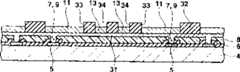
实施形态1
图1表示本发明实施形态1的半导体装置的截面图。此半导体装置具有平面矩形形状的基板1。基板1由在玻璃纤维、芳族聚酰胺纤维、液晶纤维等上浸渍环氧系树脂、聚酰亚胺树脂、BT(双马来酰亚胺·三嗪)树脂、PPE(聚亚苯基醚)等而成的物质或由硅、玻璃、陶瓷、树脂单体等绝缘材料构成。FIG. 1 shows a cross-sectional view of a semiconductor device according to
在基板1的上表面的中央部,通过由芯片焊接材料构成的粘接层3,粘接比基板1的尺寸小一定尺寸的平面矩形形状的半导体构成体2的下表面。此时,半导体构成体2具有后述的布线、柱状电极、密封膜,一般被称为CSP(chip size package),特别是,如后所述,由于采用在硅晶圆上形成布线、柱状电极、密封膜之后经切割得到各半导体构成体2的方法,也称为晶圆级CSP(W-CSP)。下面,说明半导体构成体2的结构。On the central portion of the upper surface of the
半导体构成体2包括硅基板(半导体基板)4。硅基板4通过粘接层3粘接于基板1上。在硅基板4的上面中央部设置有具有规定功能的集成电路(未图示),在上表面周边部设置有与集成电路连接的由铝系金属等构成的多个连接焊盘5。在除了连接焊盘5的中央部之外的硅基板4的上表面设置有由氧化硅等构成的绝缘膜6,通过设置在绝缘膜6上的开口部7使连接焊盘5的中央部露出。The semiconductor
在绝缘膜6的上表面上设置有由环氧系树脂或聚酰亚胺系树脂等构成的保护膜(绝缘膜)8。此情况下,在对应于绝缘膜6的开口部7的部分的保护膜8上设置有开口部9。从通过两开口部7、9露出的连接焊盘5的上表面到保护膜8的上表面的规定位置上,设置有由铜等构成的基底金属层10。在基底金属层10的整个上表面上设置有由铜构成的布线11。A protective film (insulating film) 8 made of epoxy resin, polyimide resin, or the like is provided on the upper surface of
在保护膜8的上表面的中央部的规定位置,设置有由铜等构成的散热用基底金属层12。散热用基底金属层12的整个上表面上设置有由铜构成的散热用布线13。散热用基底金属层12和散热用布线13不与任何地方连接,也可以这些彼此相连。A
在布线11的连接焊盘部上表面上设置有由铜构成的高度为50μm~200μm的柱状电极(外部连接用电极)14。在散热用布线13的连接焊盘部上表面上设置有散热用柱状电极15。在含布线11和散热用布线13的保护膜8的上表面上设置有其上表面与柱状电极14的上表面齐平的由环氧系树脂或聚酰亚胺树脂等构成的密封膜(绝缘膜)16。下面说明柱状电极14和散热用柱状电极15。柱状电极14通过布线11连接到与形成在硅基板4的主表面上的、构成集成电路的各元件和布线(未图示)相连接的连接焊盘5上,用作将这些连接到外部电路的电路连接用电极。相对于此,当驱动形成在硅基板4的主表面上的集成电路(未图示)时,散热用柱状电极15被用作散热用电极,将从该集成电路产生的热释放到外部。散热用柱状电极15的个数被设定为能够将从硅基板4产生的热充分地释放出来的数量。用与柱状电极14相同的材料和相同工序形成散热用柱状电极15时效率较高。此外,由于其高度与柱状电极14相同,优选在用与布线11相同的材料和相同的工序形成的散热用布线13上形成散热用柱状电极15。如图所示,虽然散热用布线13的宽度与图1中散热用柱状电极1 5相同并彼此分离,但优选设定为能充分吸收所产生的热量的面积,可形成宽度比散热用柱状电极15更大的结构,或者相互连接成一体。A columnar electrode (electrode for external connection) 14 made of copper and having a height of 50 μm to 200 μm is provided on the upper surface of the connection pad portion of the
如此,被称为W-CSP的半导体构成体2包括:硅基板4、连接焊盘5、绝缘膜6,并且还包括保护膜8、布线11、散热用布线13、柱状电极14、散热用柱状电极15、密封膜16。In this way, the
在半导体构成体2四周的基板1的上表面上,设置有其上表面基本上与半导体构成体2的上表面齐平的矩形框状的绝缘层17。通常,绝缘层17是所谓的预浸渍材料,例如是在玻璃纤维或芳族聚酰胺纤维上浸渍环氧系树脂或BT树脂等热固化性树脂而成的材料。On the upper surface of the
在半导体构成体2和绝缘体17的上表面上,设置有其上表面平坦的上层绝缘膜18。上层绝缘膜18是使用于增强基板的、通常被称为增强材料的材料,例如为在环氧系树脂或BT树脂等热固化性树脂中包含纤维或填料等加固材料的材料。在此情况下,纤维为玻璃纤维或芳族聚酰胺纤维等。填料为二氧化硅填料或陶瓷填料。On the upper surfaces of the semiconductor
在除了上层绝缘膜18的上表面的中央部以外的区域的规定位置处,设置有由铜等构成的上层基底金属层19。在上层基底金属层19的整个上表面上,设置有由铜构成的上层布线20。包含上层布线20的上层基底金属层19,通过设置在与柱状电极14的上表面中央部相对应的部分的上层绝缘膜18上的开口部21,与柱状电极14的上表面连接。An upper
在上层绝缘膜18的上表面中央部,以岛状形式设置有由铜等构成的散热用基底金属层22。采用与上层基底金属层19相同的材料,并以与此相同的厚度形成散热用基底金属层22。在散热用基底金属层22的整个上表面上,设置有由铜构成的散热层23。包含散热层23的散热用基底金属层22,通过设置在与散热用柱状电极15的上表面中央部相对应部分的上层绝缘膜18上的开口部24,与散热用柱状电极15的上表面连接。用相同的材料和相同的厚度形成上层布线20和散热层23。On the central part of the upper surface of the upper insulating
在包含上层布线20和散热层23的上层绝缘膜18的上表面上,设置有由阻焊剂(solder resist)等构成的外涂层膜25。在与上层布线20的连接焊盘部相对应部分的外涂层膜25中设置有开口部26。在开口部26内及其上方设置有与上层布线20的连接焊盘部相连接的焊锡球27。在除了外涂层膜25上表面的中央部之外的区域以矩阵状配置有多个焊锡球27。在与散热层23的中央部相对应部分的外涂层膜25上,设置有开口部28。由此,使散热层23的中央部通过此开口部28露出到外部。On the upper surface of the upper
如上所述,在此半导体装置中,即使具有硅基板1的半导体2的下表面、侧表面和上表面被基板1、绝缘膜17和外涂层膜18、25所覆盖,由于通过外涂层膜25的开口部28将连接于半导体构成体2的散热用柱状电极15(包括散热用布线13和散热用基底金属层12)的散热层23(包括散热用基底金属层22)露出到外部,能够改善散热性。As described above, in this semiconductor device, even if the lower surface, the side surface and the upper surface of the
其中,使基板1的尺寸比半导体构成体2大一定程度,是为了根据硅基板4上的连接焊盘5的数量的增加,使焊锡球27的配置区域比半导体构成体2的尺寸大一定程度,由此,使上层布线20的连接焊盘部(外涂层膜25的开口部26内的部分)的尺寸和间距比柱状电极14的尺寸和间距更大。The purpose of making the size of the
因此,以矩阵状配置的上层布线20的连接焊盘部,不仅限于对应于半导体构成体2的区域,也可配置在与设在半导体构成体2的侧表面的外侧的绝缘层17相对应的区域上。即,以矩阵状配置的焊锡球27中,至少最外周的焊锡球27被配置在比半导体构成体2更先靠外侧的位置的四周。Therefore, the connection pads of the
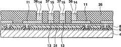
接下来,说明此半导体装置的制造方法的一个例子,首先,说明半导体构成体2的制造方法的一个例子。此情况下,首先,如图2所示,准备如下构件:在晶圆状态的硅基板4上设置有由铝系金属等构成的连接焊盘5、由氧化硅等构成的绝缘膜6和由环氧系树脂或聚酰亚胺系树脂构成的保护膜8,并且通过形成在绝缘膜6和保护膜8上的开口部7、9暴露出连接焊盘5的中央部。在上述结构中,在晶圆状态的硅基板4上,在形成各半导体构成体的区域形成有规定功能的集成电路,连接焊盘5分别与形成在相对应区域上的集成电路电连接。Next, an example of a method of manufacturing the semiconductor device will be described. First, an example of a method of manufacturing the
接下来,如图3所示,在包含通过开口部7、9露出的连接焊盘5的上表面的保护膜8的整个上表面上形成基底金属层31。此情况下,基底金属层31可以是由非电解镀形成的铜层,而且还可以是由溅射形成的铜层,还可以是在通过溅射形成的钛等薄膜层上再通过溅射形成铜层而成的材料。这与后述的上层基底金属层45的情况相同。Next, as shown in FIG. 3 ,
接下来,在基底金属层31的上表面形成镀覆抗蚀剂膜32的图案。此情况下,在与布线11形成区域和散热用布线13形成区域相对应的部分的镀覆抗蚀剂膜32上,形成有开口部33、34。接下来,通过以基底金属层31作为电镀电流通路,进行铜电解镀覆,在镀覆抗蚀剂膜32的开口部33、34内的基底金属层31的上表面上,形成布线11和散热用布线13。接下来,剥离镀覆抗蚀剂膜32。Next, a plating resist film 32 is patterned on the upper surface of the
接下来,如图4所示,在含布线11和散热用布线13的基底金属层31的上表面,形成镀覆抗蚀剂膜35的图案。此情况下,在与柱状电极14形成区域和散热用柱状电极15形成区域相对应的部分的镀覆抗蚀剂膜35中,形成开口部36、37。接下来,通过以基底金属层31作为电镀电流通路,进行铜电解镀覆,在镀覆抗蚀剂膜35的开口部36、37内的布线11和散热用布线13的连接焊盘部上表面上,形成柱状电极14和散热用柱状电极15。Next, as shown in FIG. 4 , a plating resist
接下来,剥离镀覆抗蚀剂膜35,接下来,以柱状电极14、散热用柱状电极15、布线11和散热用布线13作为掩膜,蚀刻去除基底金属层31中的不必要部分,如图5所示,仅在布线11下和散热用布线13下残留基底金属层10和散热用基底金属层12。Next, the plating resist
接下来,如图6所示,通过丝网印刷法、旋涂法、模涂法,在含柱状电极14、散热用柱状电极15、布线11和散热用布线13的保护膜8的整个上表面上,形成其厚度比柱状电极14和散热用柱状电极15的高度还要厚的由环氧系树脂或聚酰亚胺系树脂等构成的密封膜16。因此,在此状态下,柱状电极14和散热用柱状电极15的上表面就被密封膜16所覆盖。Next, as shown in FIG. 6, the entire upper surface of the
接下来,对密封膜16、柱状电极14和散热用柱状电极15的上表面侧适当地进行研磨,如图7所示,使柱状电极14和散热用柱状电极15的上表面露出,并且对含该露出的柱状电极14和散热用柱状电极15的上表面的密封膜16的上表面进行平坦化。在此,对柱状电极14和散热用柱状电极15的上表面适当进行研磨,是因为由电解电镀形成的柱状电极14和散热用电极15的高度存在偏差,而为了消除此偏差,要使柱状电极14和散热用柱状电极15的高度均一。Next, the upper surface sides of the sealing
接下来,如图8所示,将粘接层3粘接在硅基板4的整个下表面上。粘接层3由环氧系树脂、聚酰亚胺系树脂等芯片焊接材料构成,经加热加压,以半固化状态粘接在硅基板4上。接下来,将粘接在硅基板4的粘接层3粘贴在切割带(未图示)上,经过图9所示的切割工序后,剥离切割带,如图1所示,得到多个在硅基板4的下表面具有粘接层3的半导体构成体2。Next, as shown in FIG. 8 , the
在由此获得的半导体构成体2中,由于在硅基板4的下表面上具有粘接层3,因此就不需要所谓的在切割工序后在各半导体构成体2的硅基板4的下表面上分别设置粘接层的非常繁琐的作业。再有,在切割工序后剥离切割带的作业与在切割工序后在半导体构成体2的硅基板4的下表面上分别设置粘接层的作业相比,非常简单。In the
接下来,说明使用由此获得的半导体构成体2来制造图1所示的半导体装置时的一个例子。首先,如图10所示,准备平面形状为矩形形状的基板1,从中可取多片图1所示的基板1,但并不限于此。接下来,在基板1上面的多个规定位置处,分别粘接与半导体构成体2的硅基板4的下表面粘接的粘接层3。在该粘接中通过加热加压使粘接层3发生实质固化。Next, an example of manufacturing the semiconductor device shown in FIG. 1 using the thus obtained
接下来,例如,在半导体构成体2之间和配置在最外周的半导体构成体2的外侧的基板1的上表面上,以格子状确定片状的第1绝缘材料17a的位置并进行配置,并且,在其上表面上配置片状的第2绝缘材料18a。再有,也可以在配置第1绝缘材料17a之后,配置半导体构成体2。Next, for example, between the
在玻璃纤维中浸入环氧系树脂等热固化性树脂,并使热固化性树脂成为半固化状态以形成片状的预浸渍材料后,经起模加工或蚀刻等在该预浸渍材料上形成多个矩形形状的贯通孔41,就可获得格子状的第1绝缘材料17a。此情况下,为了具有平整性,第1绝缘材料17a优选形成为片状,但不一定限定于预浸渍材料,也可以是在热固化性树脂或热固化性树脂中分散玻璃纤维或二氧化硅填料等加固材料而成的材料。After impregnating thermosetting resin such as epoxy resin into glass fiber, and making the thermosetting resin into a semi-cured state to form a sheet-shaped prepreg, the prepreg is formed on the prepreg by die-cutting or etching. A rectangular through-
没有具体限定片状的第2绝缘材料18a,优选为复合(build up)材料,作为此复合材料,可举出使二氧化硅填料等混入环氧系树脂或BT树脂等的热固化性树脂中,使热固化性树脂处于半固化状态的材料。但是,作为第2绝缘材料18a,也可使用未混入上述预浸渍材料或填料的、仅由热固化性树脂构成的材料。The sheet-shaped second
在此,第1绝缘材料17a的贯通孔41的尺寸比半导体构成体2的尺寸稍微大一点。因此,在第1绝缘材料17a和半导体构成体2之间形成有间隙42。此间隙42的间隔例如为0.2mm左右。此外,第1绝缘膜17a的厚度比半导体构成体2的厚度厚,如后所述,该厚度形成为在加热加压时能够充分填埋间隙42的厚度。Here, the size of the through
接下来,使用图11所示的一对加热加压板43、44,对第1和第2绝缘材料17a、18a进行加热加压。此时,熔融于第1绝缘材料17a中的热固化性树脂被挤压,填充至如图10所示的第1绝缘材料17a和半导体构成体2之间的间隙42中,此后通过冷却,以粘接于各半导体构成体2和各半导体构成体2间的基板1的状态进行固化。由此,如图11所示,在半导体构成体2之间和配置在最外周的半导体构成体2的外侧的基板1的上表面形成上层绝缘膜18。Next, the first and second
此情况下,上层绝缘膜18的上表面由于被上侧的加热加压板43的下表面所按压,上层绝缘膜18的上表面就变成平整面。因此,不需要用于使上层绝缘膜18的上表面平坦化的研磨工序。所以,即使基板1的尺寸较大,例如为500×500mm,也可以对于配置在其上的多个半导体构成体2简单地一次性地进行上层绝缘膜18的上表面的平坦化。In this case, since the upper surface of the upper insulating
接下来,如图12所示,通过照射激光束的激光加工,在与柱状电极14和散热用柱状电极15的上表面中央部相对应的部分的上层绝缘膜18上,形成开口部21、24。接下来,根据需要,通过去污处理去除在开口部21、24内等产生的环氧污迹等。Next, as shown in FIG. 12 , openings 21 and 24 are formed on the upper
接下来,如图13所示,在含通过开口部21、24露出的柱状电极14和散热用柱状电极15的上表面的上层绝缘膜18的整个上表面形成上层基底金属层45。接下来,在上层基底金属层45的上表面上形成镀覆抗蚀剂膜46的图案。此情况下,在与上层布线20的形成区域和散热层23的形成区域相对应的部分的镀覆抗蚀剂膜46上,形成有开口部47、48。Next, as shown in FIG. 13 , upper base metal layer 45 is formed on the entire upper surface of upper insulating
接下来,通过以上层基底金属层45作为电镀电流通路,进行铜的电解电镀,在镀覆抗蚀剂膜46的开口部47、48内的上层基底金属层45的上表面上,形成上层布线20和散热层23。接下来,剥离镀覆抗蚀剂膜46,接下来,以上层布线20和散热层23作为掩膜,蚀刻并去除上层基底金属层45的不必要部分,如图14所示,仅在上层布线20和散热层23之下残留上层基底金属层19和散热用基底金属层22。Next, electrolytic plating of copper is performed by using the upper base metal layer 45 as a plating current path, and upper layer wiring is formed on the upper surface of the upper base metal layer 45 in the openings 47 and 48 of the plating resist film 46. 20 and
接下来,如图15所示,通过丝网印刷法、旋涂法等,在含上层布线20和散热层23的上层绝缘膜18的上表面上,形成由阻焊剂等构成的外涂层膜25。此情况下,在与上层布线20的连接焊盘部相对应部分的外涂层膜25上,形成开口部26。此外,在与散热层23的中央部相对应部分的第2下层绝缘膜25上,形成开口部28。Next, as shown in FIG. 15, an overcoat film made of solder resist or the like is formed on the upper surface of the upper insulating
接下来,在开口部26内及其上方形成与上层布线20的连接焊盘部相连接的焊锡球27。接下来,在相互邻接的半导体构成体2之间,切断外涂层膜25、上层绝缘膜18、绝缘膜17和基板1,就可获得多个图1所示的半导体装置。Next,
如上所述,在上述制造方法中,由于在基板1上通过粘接层3配置多个半导体构成体2,并相对于多个半导体构成体2,就可以一次性地进行上层布线20、散热层23和焊锡球27的形成,此后经切割就能得到多个半导体装置,所以能够简化制造工序。另外,在图11所示的制造工序之后,可以将基板1和多个半导体构成体2一同输送,由此也可以简化制造工序。As described above, in the above-mentioned manufacturing method, since a plurality of
实施形态2
图16表示作为本发明的实施形态2的半导体装置的截面图。在此半导体装置中,与图1所示的情况的不同之处在于:不具备散热用基底金属层12、散热用布线13、散热用柱状电极15、散热用基底金属层22、散热层23及开口部28,代替此,在基板1的下表面中央部设置有散热用基底金属层51和散热层52,通过设置在基板1上的贯通孔54,将包含散热层52的散热用基底金属层51连接到设在基板1和半导体构成体2的硅基板4之间的中继散热层53。Fig. 16 is a cross-sectional view of a semiconductor device according to
此情况下,中继散热层53由铝箔等构成,并被预先层叠在基板1的上表面的中央部。并且,通过由导电性树脂或导电性膏等构成的导电性粘接层55,将硅基板4的下表面连接到中继散热层53的上表面。使用导电性粘接层55,是为了改善从硅基板4向中继散热层53的热传导。此外,在通过激光加工在上层绝缘膜18上形成开口部21之前或形成开口部21之后,通过激光加工形成贯通孔54。还有,在形成上层基底金属层19和上层布线20的同时形成散热用基底金属层51和散热层52。In this case, the relay
因此,在该半导体装置中,也是即使具有硅基板1的半导体构成体2的下表面、侧表面和上表面被基板1、绝缘层17和上层绝缘膜18、外涂层膜25所覆盖,由于通过导电性粘接层55和中继散热层53与半导体构成体2的硅基板4连接的散热层52(包含散热用基底金属层51)从基板1的下表面露出来,也能够改善半导体装置的散热性。Therefore, in this semiconductor device, even if the lower surface, side surfaces, and upper surface of the
实施形态3
图17表示作为本发明实施形态3的半导体装置的截面图。在此半导体装置中,具备有图1所示的散热层23等和图16所示的散热层52等。因此,在此半导体装置中,能够进一步改善散热性。Fig. 17 is a cross-sectional view of a semiconductor device as
实施形态4
在上述实施形态1中,如图1所示,说明了在上层绝缘膜18上仅形成1层上层布线20的情况,但并不限定于此,也可以形成两层以上,例如,如图18所示的本发明的实施形态4,也可以是两层。即,在半导体构成体2和绝缘层17的上表面上,设置有由复合材料等构成的第1上层绝缘膜61。In the above-mentioned first embodiment, as shown in FIG. 1 , the case where only one layer of
在除了第1上层绝缘膜61的上表面的中央部之外的区域,设置有通过形成在第1上层绝缘膜61的开口部64连接于半导体构成体2的柱状电极14的上表面的含第1上层基底金属层62的第1上层布线63。在第1上层绝缘膜61的上表面中央部,设置有通过形成在第1上层绝缘膜61的开口部67连接于半导体构成体2的散热用柱状电极15的上表面的含中继基底金属层65的中继散热层66。In a region other than the central portion of the upper surface of the first upper insulating film 61, there is provided a layer including a second electrode connected to the upper surface of the
在含第1上层布线63和中继散热层66的第1上层绝缘膜61的上表面上,设置有由复合材料等构成的第2上层绝缘膜68。在除了第2上层绝缘膜68的上表面的中央部之外的区域,设置有通过形成在第2上层绝缘膜68的开口部71连接于第1上层布线63的连接焊盘的含第2上层基底金属层69的第2上层布线70。在第2上层绝缘膜68的上表面中央部处,设置有通过形成在第2上层绝缘膜68的开口部74连接于中继散热层66的含散热用基底金属层72的散热层73。On the upper surface of the first upper insulating film 61 including the first upper wiring 63 and the relay heat dissipation layer 66, a second upper insulating film 68 made of composite material or the like is provided. In a region other than the central portion of the upper surface of the second upper insulating film 68, a second upper layer including a connection pad connected to the first upper layer wiring 63 through the opening 71 formed in the second upper insulating film 68 is provided. The second upper layer wiring 70 of the base metal layer 69 . At the central portion of the upper surface of the second upper insulating film 68, a heat dissipation layer 73 including a heat dissipation base metal layer 72 connected to the relay heat dissipation layer 66 through an opening 74 formed in the second upper insulating film 68 is provided.
在含第2上层布线70和散热层73的第2上层绝缘膜68的上表面上,设置有由阻焊剂等构成的外涂层膜75。在与第2上层布线70的连接焊盘部相对应部分的外涂层膜75上,设置有开口部76。在开口部76内及其上方设置有连接于第2上层布线70的连接焊盘部的焊锡球77。在与散热层73的中央部相对应部分的外涂层膜75上,设置有开口部78。因此,通过此开口部78使散热层73的中央部露出在外面。On the upper surface of the second upper layer insulating film 68 including the second upper layer wiring 70 and the heat dissipation layer 73, an overcoat film 75 made of solder resist or the like is provided. An opening 76 is provided on the overcoat film 75 at a portion corresponding to the connection pad portion of the second upper layer wiring 70 . Solder balls 77 connected to the connection pads of the second upper layer wiring 70 are provided in and above the opening 76 . An opening 78 is provided on the overcoat film 75 at a portion corresponding to the central portion of the heat dissipation layer 73 . Therefore, the central portion of the heat dissipation layer 73 is exposed to the outside through the opening 78 .
实施形态5
图19中图示出的实施形态5,相对于图17中示出的实施形态3,具有下面所示的不同点。
第1不同点是在散热层23上也设置有焊球80。此情况下,外涂层膜25形成在除尺寸适于形成散热用焊球80的开口部以外的部位上,即也覆盖散热层23。虽未图示,但散热用的焊球80能够与电路基板的散热路径或外部散热板相结合,所以能够进一步提高散热性。第2不同点是在基板1的下表面上设置有外涂层膜81。外涂层膜81具有露出散热层52的开口部83。作为此实施形态的变化例,也可在散热层52上设置散热用焊锡球。即,可以从仅在散热层23上设置散热用的焊锡球、仅在散热层52上设置散热用的焊锡球、在散热层23上和散热层52上的双方都设置散热用的焊锡球等状态中任意选择。The first difference is that the
实施形态6
图20中示出的实施形态6为表示,并不是在上层布线侧上而是在整个半导体构成体2的底面侧设置有焊锡球的一个例子。下面,说明此实施形态的结构。
在上层绝缘膜18的上表面中央部以实地(ベタ)状设置有由铜等构成的散热用上层基底金属层22。在散热用上层基底金属层22的整个上表面上,设置有由铜构成的上层散热层23。通过上层绝缘膜18的开口部21,含散热用上层基底金属层22的上层散热层23与所有的散热用柱状电极15的上表面相连接。An upper
在含上层布线20和上层散热层23的上层绝缘膜18的上表面上,设置有由阻焊剂等构成的上层外涂层膜25。在与上层散热层23的中央部相对应部分的上层外涂层膜25上,设置有开口部28。因此,通过此开口部28使上层散热层23的中央部露出在外面。On the upper surface of the upper
在基板1的中央部,设置有多个开口部54。在除了基板1的下表面的中央部之外的区域,设置有由铜等构成下层基底金属层86。在下层基底金属层86的整个下表面上,设置有下层布线87。在基板1的下表面中央部以实地(ベタ)状设置有由铜等构成的散热用下层基底金属层51。在散热用下层基底金属层51的整个下表面上,设置有下层散热层52。通过基板1的开口部54,含散热用下层基底金属层51的下层散热层52与内部散热层55进行连接。In the central portion of the
在含下层布线87和下层散热层52的基板1的下表面上,设置有由阻焊剂等构成的下层外涂层膜89。在与下层布线87的连接焊盘部相对应部分的下层外涂层膜89上,设置有开口部88。此外,在与下层散热层52的规定的多个位置相对应部分的下层外涂层膜89上,设置有开口部94。On the lower surface of the
在开口部88内及其下方,设置有与下层布线87的连接焊盘部连接的作为外部连接用电极的焊锡球90。在开口部94内及其下方,设置有连接于下层散热层52的散热用焊锡91。在除了下层外涂层膜89下的中央部之外的区域以矩阵状设置有多个焊锡球90。多个散热用焊锡球91以矩阵状设置在下层外涂层膜89下的中央部。
在上层绝缘膜18、绝缘层17和基板1的规定的多个位置设置有贯通孔84。贯通孔84的内壁面设置有由由铜等构成的基底金属层85a和铜层85b所构成的上下导通部85。上下导通部85的上部连接于上层布线20。上下导通部85的下部连接于下层布线87。在上下导通部85内填充有由阻焊剂等构成的填充材料86。Through-
在此,作为外部连接用电极的焊锡球90,通过下层布线87、上下导通部85和上层布线23,连接于作为半导体构成体3的外部连接用电极的柱状电极14。散热用焊锡球91,通过下层散热层52(包含散热用下层基底金属层51)、内部散热层55和粘接层3,热连接于半导体构成体2的硅基板4的下表面。Here,
如此,在本实施形态中,因为能以面朝上方式焊接半导体构成体2,所以能够降低因与所连接的电路基板的线膨胀系数不同而产生的应力影响。此外,也可适用于在上表面侧具有摄像元件的光敏器件的接合。In this way, in this embodiment, since the
再有,也能够在上层布线侧设置焊锡球。此情况下,能够形成为层叠多层这种半导体装置而成的结构。In addition, solder balls can also be provided on the upper layer wiring side. In this case, it is possible to form a structure in which multiple layers of such semiconductor devices are stacked.
进而,在上述各实施形态中,半导体构成体2中作为外部连接用电极具有设置在布线11的连接焊盘部的柱状电极14,但并不限定于此。例如,半导体构成体2中可以具备具有作为外部连接用电极的连接焊盘部的布线11,此外,还可以具有作为外部连接用电极的连接焊盘5,而且也可以作为外部连接用电极具有设置在连接焊盘5上的柱状电极。并且,在上述实施形态中,基板1为单片构件,此基板5也可为将绝缘膜和布线交替层叠的多层印刷电路板。但是,在此基板5上形成散热层的情况下,优选在最下层的绝缘层的下表面形成散热层,并至少使其一部分暴露到外部。此外,在基板5的下表面形成散热层的情况下,也可暴露散热层并用外涂层膜覆盖基板的下表面。Furthermore, in each of the above-mentioned embodiments, the
根据本发明,即使具有半导体基板的半导体构成体的下表面、侧表面和上表面被基板、绝缘层和上层绝缘膜所覆盖,由于使连接半导体构成体的散热层暴露到外部,因此也能够改善散热性。According to the present invention, even if the lower surface, the side surface and the upper surface of the semiconductor structure having the semiconductor substrate are covered by the substrate, the insulating layer and the upper insulating film, since the heat dissipation layer connecting the semiconductor structure is exposed to the outside, it is possible to improve Heat dissipation.
Claims (19)
Translated fromChineseApplications Claiming Priority (2)
| Application Number | Priority Date | Filing Date | Title |
|---|---|---|---|
| JP2003328911 | 2003-09-19 | ||
| JP2003328911AJP4012496B2 (en) | 2003-09-19 | 2003-09-19 | Semiconductor device |
Publications (2)
| Publication Number | Publication Date |
|---|---|
| CN1619787Atrue CN1619787A (en) | 2005-05-25 |
| CN1322566C CN1322566C (en) | 2007-06-20 |
Family
ID=34308837
Family Applications (1)
| Application Number | Title | Priority Date | Filing Date |
|---|---|---|---|
| CNB2004101047355AExpired - LifetimeCN1322566C (en) | 2003-09-19 | 2004-09-16 | Semiconductor device |
Country Status (4)
| Country | Link |
|---|---|
| US (1) | US7042081B2 (en) |
| JP (1) | JP4012496B2 (en) |
| KR (1) | KR100637307B1 (en) |
| CN (1) | CN1322566C (en) |
Cited By (14)
| Publication number | Priority date | Publication date | Assignee | Title |
|---|---|---|---|---|
| CN100456466C (en)* | 2005-07-13 | 2009-01-28 | 精工爱普生株式会社 | Semiconductor device |
| CN102439719A (en)* | 2009-05-14 | 2012-05-02 | 米辑电子股份有限公司 | System-in packages |
| CN103918057A (en)* | 2011-08-16 | 2014-07-09 | 先进模拟科技公司 | Bump-on-leadframe semiconductor package with low thermal resistance |
| CN105428327A (en)* | 2014-08-28 | 2016-03-23 | 联华电子股份有限公司 | Fan-out type wafer level package structure |
| CN106158782A (en)* | 2015-03-23 | 2016-11-23 | 矽品精密工业股份有限公司 | Electronic package and manufacturing method thereof |
| CN106575624A (en)* | 2014-08-18 | 2017-04-19 | 高通股份有限公司 | Integrated device that includes a heat dissipation layer that provides an electrical path for ground signals |
| CN107004640A (en)* | 2014-12-16 | 2017-08-01 | 高通股份有限公司 | The systems, devices and methods being grounded for semiconductor packages |
| CN110634805A (en)* | 2018-06-21 | 2019-12-31 | 奥特斯奥地利科技与系统技术有限公司 | Component carrier and method for producing the component carrier |
| CN110959189A (en)* | 2017-08-01 | 2020-04-03 | 株式会社村田制作所 | High frequency module |
| TWI720145B (en)* | 2016-06-13 | 2021-03-01 | 南韓商三星電子股份有限公司 | Method of fabricating a fan-out panel level package and a carrier tape film therefor |
| CN113284866A (en)* | 2020-02-20 | 2021-08-20 | 住友电气工业株式会社 | Semiconductor device and method for manufacturing the same |
| WO2021203726A1 (en)* | 2020-04-10 | 2021-10-14 | 青岛歌尔智能传感器有限公司 | Sensor and manufacturing method therefor, and electronic device |
| WO2022110936A1 (en)* | 2020-11-26 | 2022-06-02 | 苏州矽锡谷半导体科技有限公司 | Power element packaging structure and manufacturing method therefor |
| CN119542158A (en)* | 2025-01-22 | 2025-02-28 | 深圳市晶存科技股份有限公司 | Packaging method and structure of LPCAMM memory module |
Families Citing this family (50)
| Publication number | Priority date | Publication date | Assignee | Title |
|---|---|---|---|---|
| JP3979404B2 (en)* | 2004-06-30 | 2007-09-19 | カシオ計算機株式会社 | Semiconductor device |
| JP4093186B2 (en) | 2004-01-27 | 2008-06-04 | カシオ計算機株式会社 | Manufacturing method of semiconductor device |
| JP3945483B2 (en)* | 2004-01-27 | 2007-07-18 | カシオ計算機株式会社 | Manufacturing method of semiconductor device |
| DE102004018475A1 (en)* | 2004-04-16 | 2005-11-10 | eupec Europäische Gesellschaft für Leistungshalbleiter mbH | A power semiconductor device |
| JP2006173232A (en)* | 2004-12-14 | 2006-06-29 | Casio Comput Co Ltd | Semiconductor device and manufacturing method thereof |
| JP4725178B2 (en)* | 2005-04-28 | 2011-07-13 | カシオ計算機株式会社 | Semiconductor device and manufacturing method thereof |
| US7468545B2 (en)* | 2005-05-06 | 2008-12-23 | Megica Corporation | Post passivation structure for a semiconductor device and packaging process for same |
| US7582556B2 (en) | 2005-06-24 | 2009-09-01 | Megica Corporation | Circuitry component and method for forming the same |
| JP4289335B2 (en)* | 2005-08-10 | 2009-07-01 | セイコーエプソン株式会社 | Electronic components, circuit boards and electronic equipment |
| JP4817796B2 (en)* | 2005-10-18 | 2011-11-16 | Okiセミコンダクタ株式会社 | Semiconductor device and manufacturing method thereof |
| JP2007294652A (en)* | 2006-04-25 | 2007-11-08 | Matsushita Electric Ind Co Ltd | Semiconductor integrated circuit device and manufacturing method thereof |
| JP4193897B2 (en)* | 2006-05-19 | 2008-12-10 | カシオ計算機株式会社 | Semiconductor device and manufacturing method thereof |
| US20080116564A1 (en)* | 2006-11-21 | 2008-05-22 | Advanced Chip Engineering Technology Inc. | Wafer level package with die receiving cavity and method of the same |
| US7911044B2 (en)* | 2006-12-29 | 2011-03-22 | Advanced Chip Engineering Technology Inc. | RF module package for releasing stress |
| US20080157316A1 (en)* | 2007-01-03 | 2008-07-03 | Advanced Chip Engineering Technology Inc. | Multi-chips package and method of forming the same |
| US20080157342A1 (en)* | 2007-01-03 | 2008-07-03 | Advanced Chip Engineering Technology Inc. | Package with a marking structure and method of the same |
| TW200901409A (en)* | 2007-06-22 | 2009-01-01 | Nan Ya Printed Circuit Board Corp | Packaging substrate with embedded chip and buried heatsink |
| US7868445B2 (en)* | 2007-06-25 | 2011-01-11 | Epic Technologies, Inc. | Integrated structures and methods of fabrication thereof with fan-out metallization on a chips-first chip layer |
| JP2009016818A (en)* | 2007-07-04 | 2009-01-22 | Samsung Electro-Mechanics Co Ltd | Multilayer printed circuit board and method of manufacturing the same |
| US7915728B2 (en)* | 2007-07-12 | 2011-03-29 | Vishay General Semiconductor Llc | Subassembly that includes a power semiconductor die and a heat sink having an exposed surface portion thereof |
| US20090079072A1 (en)* | 2007-09-21 | 2009-03-26 | Casio Computer Co., Ltd. | Semiconductor device having low dielectric insulating film and manufacturing method of the same |
| US8587124B2 (en) | 2007-09-21 | 2013-11-19 | Teramikros, Inc. | Semiconductor device having low dielectric insulating film and manufacturing method of the same |
| KR101143837B1 (en)* | 2007-10-15 | 2012-07-12 | 삼성테크윈 주식회사 | Electronic chip embedded circuit board and method of manufacturing the same |
| JP4666028B2 (en)* | 2008-03-31 | 2011-04-06 | カシオ計算機株式会社 | Semiconductor device |
| US8354304B2 (en)* | 2008-12-05 | 2013-01-15 | Stats Chippac, Ltd. | Semiconductor device and method of forming conductive posts embedded in photosensitive encapsulant |
| US8169065B2 (en)* | 2009-12-22 | 2012-05-01 | Epic Technologies, Inc. | Stackable circuit structures and methods of fabrication thereof |
| KR101124110B1 (en)* | 2010-02-16 | 2012-03-21 | 삼성전기주식회사 | Semiconductor chip package and method for manufacturing the same |
| US8558392B2 (en)* | 2010-05-14 | 2013-10-15 | Stats Chippac, Ltd. | Semiconductor device and method of forming interconnect structure and mounting semiconductor die in recessed encapsulant |
| US10115654B2 (en)* | 2010-06-18 | 2018-10-30 | Palo Alto Research Center Incorporated | Buried thermally conductive layers for heat extraction and shielding |
| KR20120026855A (en)* | 2010-09-10 | 2012-03-20 | 삼성전기주식회사 | Embedded ball grid array substrate and manufacturing method thereof |
| KR101131288B1 (en)* | 2010-12-06 | 2012-03-30 | 삼성전기주식회사 | A method of manufacturing printed circuit board |
| US8552540B2 (en)* | 2011-05-10 | 2013-10-08 | Conexant Systems, Inc. | Wafer level package with thermal pad for higher power dissipation |
| US20130146345A1 (en)* | 2011-12-12 | 2013-06-13 | Kazuki KAJIHARA | Printed wiring board and method for manufacturing the same |
| US8912670B2 (en)* | 2012-09-28 | 2014-12-16 | Intel Corporation | Bumpless build-up layer package including an integrated heat spreader |
| US9136236B2 (en) | 2012-09-28 | 2015-09-15 | Intel Corporation | Localized high density substrate routing |
| US9190380B2 (en) | 2012-12-06 | 2015-11-17 | Intel Corporation | High density substrate routing in BBUL package |
| JP5716972B2 (en)* | 2013-02-05 | 2015-05-13 | 株式会社デンソー | Electronic component heat dissipation structure and method of manufacturing the same |
| US9159690B2 (en) | 2013-09-25 | 2015-10-13 | Intel Corporation | Tall solders for through-mold interconnect |
| US9349703B2 (en) | 2013-09-25 | 2016-05-24 | Intel Corporation | Method for making high density substrate interconnect using inkjet printing |
| JP2015146346A (en)* | 2014-01-31 | 2015-08-13 | イビデン株式会社 | multilayer wiring board |
| JP6457206B2 (en)* | 2014-06-19 | 2019-01-23 | 株式会社ジェイデバイス | Semiconductor package and manufacturing method thereof |
| US9633934B2 (en) | 2014-11-26 | 2017-04-25 | Taiwan Semiconductor Manufacturing Company, Ltd. | Semicondutor device and method of manufacture |
| KR101927572B1 (en) | 2015-03-17 | 2018-12-10 | 앰코테크놀로지코리아(주) | Semiconductor Device And Fabricating Method Thereof |
| TWM524553U (en)* | 2016-03-21 | 2016-06-21 | Team Expert Man Consulting Service Ltd | Semiconductor package structure |
| KR102815722B1 (en)* | 2016-11-09 | 2025-06-04 | 삼성전자주식회사 | Semiconductor package, manufacturing method thereof, and electronic component module using the same |
| US10347574B2 (en)* | 2017-09-28 | 2019-07-09 | Taiwan Semiconductor Manufacturing Co., Ltd. | Integrated fan-out packages |
| KR102163059B1 (en)* | 2018-09-07 | 2020-10-08 | 삼성전기주식회사 | Printed circuit board with embedded interconnect structure |
| TWI697081B (en)* | 2019-06-10 | 2020-06-21 | 恆勁科技股份有限公司 | Semiconductor package substrate, and manufacturing method and electronic package thereof |
| US20220415807A1 (en)* | 2021-06-25 | 2022-12-29 | Intel Corporation | Thermal management structures in semiconductor devices and methods of fabrication |
| CN119364634A (en)* | 2023-07-24 | 2025-01-24 | 庆鼎精密电子(淮安)有限公司 | Circuit board and manufacturing method thereof |
Family Cites Families (8)
| Publication number | Priority date | Publication date | Assignee | Title |
|---|---|---|---|---|
| JPH0756887B2 (en)* | 1988-04-04 | 1995-06-14 | 株式会社日立製作所 | Semiconductor package and computer using the same |
| JP2001044246A (en)* | 1999-08-04 | 2001-02-16 | Sony Corp | Semiconductor device and manufacture thereof |
| US20020030276A1 (en)* | 2000-04-27 | 2002-03-14 | Guo-Quan Lu | Dimple array interconnect technique for semiconductor device |
| JP3664432B2 (en) | 2000-05-18 | 2005-06-29 | カシオ計算機株式会社 | Semiconductor device and manufacturing method thereof |
| JP3520039B2 (en)* | 2000-10-05 | 2004-04-19 | 三洋電機株式会社 | Semiconductor device and semiconductor module |
| TW577160B (en)* | 2002-02-04 | 2004-02-21 | Casio Computer Co Ltd | Semiconductor device and manufacturing method thereof |
| US6770971B2 (en)* | 2002-06-14 | 2004-08-03 | Casio Computer Co., Ltd. | Semiconductor device and method of fabricating the same |
| JP2003142525A (en)* | 2002-11-11 | 2003-05-16 | Toshiba Corp | Semiconductor device |
- 2003
- 2003-09-19JPJP2003328911Apatent/JP4012496B2/ennot_activeExpired - Fee Related
- 2004
- 2004-09-13USUS10/940,232patent/US7042081B2/ennot_activeExpired - Lifetime
- 2004-09-16KRKR1020040074047Apatent/KR100637307B1/ennot_activeExpired - Fee Related
- 2004-09-16CNCNB2004101047355Apatent/CN1322566C/ennot_activeExpired - Lifetime
Cited By (19)
| Publication number | Priority date | Publication date | Assignee | Title |
|---|---|---|---|---|
| CN100456466C (en)* | 2005-07-13 | 2009-01-28 | 精工爱普生株式会社 | Semiconductor device |
| CN102439719A (en)* | 2009-05-14 | 2012-05-02 | 米辑电子股份有限公司 | System-in packages |
| CN102439719B (en)* | 2009-05-14 | 2015-06-24 | 高通股份有限公司 | System-in packages |
| CN103918057A (en)* | 2011-08-16 | 2014-07-09 | 先进模拟科技公司 | Bump-on-leadframe semiconductor package with low thermal resistance |
| CN106575624A (en)* | 2014-08-18 | 2017-04-19 | 高通股份有限公司 | Integrated device that includes a heat dissipation layer that provides an electrical path for ground signals |
| CN106575624B (en)* | 2014-08-18 | 2019-02-12 | 高通股份有限公司 | Integrated devices that include heat dissipation layers that provide electrical paths for ground signals |
| CN105428327B (en)* | 2014-08-28 | 2018-03-23 | 联华电子股份有限公司 | Fan-out type wafer level package structure |
| CN105428327A (en)* | 2014-08-28 | 2016-03-23 | 联华电子股份有限公司 | Fan-out type wafer level package structure |
| CN107004640A (en)* | 2014-12-16 | 2017-08-01 | 高通股份有限公司 | The systems, devices and methods being grounded for semiconductor packages |
| CN107004640B (en)* | 2014-12-16 | 2020-04-10 | 高通股份有限公司 | System, apparatus and method for semiconductor package grounding |
| CN106158782A (en)* | 2015-03-23 | 2016-11-23 | 矽品精密工业股份有限公司 | Electronic package and manufacturing method thereof |
| TWI720145B (en)* | 2016-06-13 | 2021-03-01 | 南韓商三星電子股份有限公司 | Method of fabricating a fan-out panel level package and a carrier tape film therefor |
| CN110959189A (en)* | 2017-08-01 | 2020-04-03 | 株式会社村田制作所 | High frequency module |
| CN110634805A (en)* | 2018-06-21 | 2019-12-31 | 奥特斯奥地利科技与系统技术有限公司 | Component carrier and method for producing the component carrier |
| CN110634805B (en)* | 2018-06-21 | 2024-03-08 | 奥特斯奥地利科技与系统技术有限公司 | Component carrier and method for manufacturing the same |
| CN113284866A (en)* | 2020-02-20 | 2021-08-20 | 住友电气工业株式会社 | Semiconductor device and method for manufacturing the same |
| WO2021203726A1 (en)* | 2020-04-10 | 2021-10-14 | 青岛歌尔智能传感器有限公司 | Sensor and manufacturing method therefor, and electronic device |
| WO2022110936A1 (en)* | 2020-11-26 | 2022-06-02 | 苏州矽锡谷半导体科技有限公司 | Power element packaging structure and manufacturing method therefor |
| CN119542158A (en)* | 2025-01-22 | 2025-02-28 | 深圳市晶存科技股份有限公司 | Packaging method and structure of LPCAMM memory module |
Also Published As
| Publication number | Publication date |
|---|---|
| JP2005093942A (en) | 2005-04-07 |
| KR20050028791A (en) | 2005-03-23 |
| US20050062147A1 (en) | 2005-03-24 |
| KR100637307B1 (en) | 2006-10-25 |
| JP4012496B2 (en) | 2007-11-21 |
| US7042081B2 (en) | 2006-05-09 |
| CN1322566C (en) | 2007-06-20 |
Similar Documents
| Publication | Publication Date | Title |
|---|---|---|
| CN1619787A (en) | Semiconductor device | |
| CN100343965C (en) | Semiconductor device having conducting portion of upper and lower conductive layers, and method of fabricating the same | |
| CN1298034C (en) | Semiconductor package having semiconductor constructing body and method of manufacturing the same | |
| CN1649119A (en) | Semiconductor device | |
| CN1649139A (en) | Semiconductor device and manufacturing method thereof | |
| CN1269199C (en) | Flip chip type semiconductor device and making method thereof | |
| CN100350607C (en) | Semiconductor device and manufacturing method thereof | |
| TWI278048B (en) | Semiconductor device and its manufacturing method | |
| CN1097313C (en) | Manufacturing method of lead frame | |
| US7183639B2 (en) | Semiconductor device and method of manufacturing the same | |
| CN1758433A (en) | Semiconductor device and manufacturing method thereof | |
| JP4730426B2 (en) | Mounting substrate and semiconductor module | |
| CN1633705A (en) | Semiconductor device and manufacturing method thereof | |
| CN100397629C (en) | Semiconductor device and method for manufacturing the same | |
| JP2020004926A (en) | Wiring board and method of manufacturing wiring board | |
| CN1830083A (en) | Semiconductor device and manufacturing method thereof | |
| JP4438389B2 (en) | Manufacturing method of semiconductor device | |
| JP4316624B2 (en) | Semiconductor device | |
| CN1725474A (en) | Circuit device and manufacturing method thereof | |
| JP4321758B2 (en) | Semiconductor device | |
| JP4241284B2 (en) | Semiconductor device | |
| TWI248148B (en) | Semiconductor device having heat dissipation layer cross-reference to related applications | |
| JP3979404B2 (en) | Semiconductor device | |
| JP4561079B2 (en) | Manufacturing method of semiconductor device |
Legal Events
| Date | Code | Title | Description |
|---|---|---|---|
| C06 | Publication | ||
| PB01 | Publication | ||
| C10 | Entry into substantive examination | ||
| SE01 | Entry into force of request for substantive examination | ||
| C14 | Grant of patent or utility model | ||
| GR01 | Patent grant | ||
| ASS | Succession or assignment of patent right | Owner name:CASIO COMPUTER CO., LTD.;CMK CO., LTD. Free format text:FORMER OWNER: CASIO COMPUTER CO., LTD. Effective date:20070518 | |
| C41 | Transfer of patent application or patent right or utility model | ||
| TR01 | Transfer of patent right | Effective date of registration:20070518 Address after:Tokyo, Japan Co-patentee after:Cmk Corp. Patentee after:CASIO COMPUTER Co.,Ltd. Address before:Tokyo, Japan Patentee before:CASIO COMPUTER Co.,Ltd. | |
| ASS | Succession or assignment of patent right | Owner name:ZHAOZHUANGWEI CO., LTD. Free format text:FORMER OWNER: CASIO COMPUTER CO., LTD. Effective date:20120305 | |
| C41 | Transfer of patent application or patent right or utility model | ||
| TR01 | Transfer of patent right | Effective date of registration:20120305 Address after:Tokyo, Japan Co-patentee after:Cmk Corp. Patentee after:Zhaozhuang Micro Co.,Ltd. Address before:Tokyo, Japan Co-patentee before:Cmk Corp. Patentee before:CASIO COMPUTER Co.,Ltd. | |
| C41 | Transfer of patent application or patent right or utility model | ||
| TR01 | Transfer of patent right | Effective date of registration:20161213 Address after:Japan Kagawa Patentee after:AOI ELECTRONICS Co.,Ltd. Patentee after:Cmk Corp. Address before:Kanagawa, Japan Patentee before:Zhao Tan Jing Co.,Ltd. Patentee before:Cmk Corp. Effective date of registration:20161213 Address after:Kanagawa, Japan Patentee after:Zhao Tan Jing Co.,Ltd. Patentee after:Cmk Corp. Address before:Tokyo, Japan Patentee before:Zhaozhuang Micro Co.,Ltd. Patentee before:Cmk Corp. | |
| TR01 | Transfer of patent right | ||
| TR01 | Transfer of patent right | Effective date of registration:20210723 Address after:Kanagawa, Japan Patentee after:AOI ELECTRONICS Co.,Ltd. Address before:Japan Kagawa Patentee before:AOI ELECTRONICS Co.,Ltd. Patentee before:CMK Corp. | |
| CX01 | Expiry of patent term | Granted publication date:20070620 | |
| CX01 | Expiry of patent term |