CN1608400A - Chip scale stacking system and method - Google Patents
Chip scale stacking system and methodDownload PDFInfo
- Publication number
- CN1608400A CN1608400ACNA028261879ACN02826187ACN1608400ACN 1608400 ACN1608400 ACN 1608400ACN A028261879 ACNA028261879 ACN A028261879ACN 02826187 ACN02826187 ACN 02826187ACN 1608400 ACN1608400 ACN 1608400A
- Authority
- CN
- China
- Prior art keywords
- csp
- flex
- contacts
- contact
- module
- Prior art date
- Legal status (The legal status is an assumption and is not a legal conclusion. Google has not performed a legal analysis and makes no representation as to the accuracy of the status listed.)
- Granted
Links
Images


Classifications
- H—ELECTRICITY
- H05—ELECTRIC TECHNIQUES NOT OTHERWISE PROVIDED FOR
- H05K—PRINTED CIRCUITS; CASINGS OR CONSTRUCTIONAL DETAILS OF ELECTRIC APPARATUS; MANUFACTURE OF ASSEMBLAGES OF ELECTRICAL COMPONENTS
- H05K1/00—Printed circuits
- H05K1/02—Details
- H05K1/14—Structural association of two or more printed circuits
- H05K1/141—One or more single auxiliary printed circuits mounted on a main printed circuit, e.g. modules, adapters
- H—ELECTRICITY
- H01—ELECTRIC ELEMENTS
- H01L—SEMICONDUCTOR DEVICES NOT COVERED BY CLASS H10
- H01L23/00—Details of semiconductor or other solid state devices
- H01L23/28—Encapsulations, e.g. encapsulating layers, coatings, e.g. for protection
- H01L23/31—Encapsulations, e.g. encapsulating layers, coatings, e.g. for protection characterised by the arrangement or shape
- H01L23/3107—Encapsulations, e.g. encapsulating layers, coatings, e.g. for protection characterised by the arrangement or shape the device being completely enclosed
- H01L23/3114—Encapsulations, e.g. encapsulating layers, coatings, e.g. for protection characterised by the arrangement or shape the device being completely enclosed the device being a chip scale package, e.g. CSP
- H—ELECTRICITY
- H01—ELECTRIC ELEMENTS
- H01L—SEMICONDUCTOR DEVICES NOT COVERED BY CLASS H10
- H01L23/00—Details of semiconductor or other solid state devices
- H01L23/48—Arrangements for conducting electric current to or from the solid state body in operation, e.g. leads, terminal arrangements ; Selection of materials therefor
- H01L23/488—Arrangements for conducting electric current to or from the solid state body in operation, e.g. leads, terminal arrangements ; Selection of materials therefor consisting of soldered or bonded constructions
- H01L23/498—Leads, i.e. metallisations or lead-frames on insulating substrates, e.g. chip carriers
- H01L23/49811—Additional leads joined to the metallisation on the insulating substrate, e.g. pins, bumps, wires, flat leads
- H01L23/49816—Spherical bumps on the substrate for external connection, e.g. ball grid arrays [BGA]
- H—ELECTRICITY
- H01—ELECTRIC ELEMENTS
- H01L—SEMICONDUCTOR DEVICES NOT COVERED BY CLASS H10
- H01L23/00—Details of semiconductor or other solid state devices
- H01L23/48—Arrangements for conducting electric current to or from the solid state body in operation, e.g. leads, terminal arrangements ; Selection of materials therefor
- H01L23/488—Arrangements for conducting electric current to or from the solid state body in operation, e.g. leads, terminal arrangements ; Selection of materials therefor consisting of soldered or bonded constructions
- H01L23/498—Leads, i.e. metallisations or lead-frames on insulating substrates, e.g. chip carriers
- H01L23/49827—Via connections through the substrates, e.g. pins going through the substrate, coaxial cables
- H—ELECTRICITY
- H01—ELECTRIC ELEMENTS
- H01L—SEMICONDUCTOR DEVICES NOT COVERED BY CLASS H10
- H01L23/00—Details of semiconductor or other solid state devices
- H01L23/48—Arrangements for conducting electric current to or from the solid state body in operation, e.g. leads, terminal arrangements ; Selection of materials therefor
- H01L23/488—Arrangements for conducting electric current to or from the solid state body in operation, e.g. leads, terminal arrangements ; Selection of materials therefor consisting of soldered or bonded constructions
- H01L23/498—Leads, i.e. metallisations or lead-frames on insulating substrates, e.g. chip carriers
- H01L23/4985—Flexible insulating substrates
- H—ELECTRICITY
- H01—ELECTRIC ELEMENTS
- H01L—SEMICONDUCTOR DEVICES NOT COVERED BY CLASS H10
- H01L23/00—Details of semiconductor or other solid state devices
- H01L23/52—Arrangements for conducting electric current within the device in operation from one component to another, i.e. interconnections, e.g. wires, lead frames
- H01L23/538—Arrangements for conducting electric current within the device in operation from one component to another, i.e. interconnections, e.g. wires, lead frames the interconnection structure between a plurality of semiconductor chips being formed on, or in, insulating substrates
- H01L23/5387—Flexible insulating substrates
- H—ELECTRICITY
- H01—ELECTRIC ELEMENTS
- H01L—SEMICONDUCTOR DEVICES NOT COVERED BY CLASS H10
- H01L25/00—Assemblies consisting of a plurality of semiconductor or other solid state devices
- H01L25/03—Assemblies consisting of a plurality of semiconductor or other solid state devices all the devices being of a type provided for in a single subclass of subclasses H10B, H10D, H10F, H10H, H10K or H10N, e.g. assemblies of rectifier diodes
- H01L25/04—Assemblies consisting of a plurality of semiconductor or other solid state devices all the devices being of a type provided for in a single subclass of subclasses H10B, H10D, H10F, H10H, H10K or H10N, e.g. assemblies of rectifier diodes the devices not having separate containers
- H01L25/065—Assemblies consisting of a plurality of semiconductor or other solid state devices all the devices being of a type provided for in a single subclass of subclasses H10B, H10D, H10F, H10H, H10K or H10N, e.g. assemblies of rectifier diodes the devices not having separate containers the devices being of a type provided for in group H10D89/00
- H01L25/0657—Stacked arrangements of devices
- H—ELECTRICITY
- H01—ELECTRIC ELEMENTS
- H01L—SEMICONDUCTOR DEVICES NOT COVERED BY CLASS H10
- H01L25/00—Assemblies consisting of a plurality of semiconductor or other solid state devices
- H01L25/03—Assemblies consisting of a plurality of semiconductor or other solid state devices all the devices being of a type provided for in a single subclass of subclasses H10B, H10D, H10F, H10H, H10K or H10N, e.g. assemblies of rectifier diodes
- H01L25/10—Assemblies consisting of a plurality of semiconductor or other solid state devices all the devices being of a type provided for in a single subclass of subclasses H10B, H10D, H10F, H10H, H10K or H10N, e.g. assemblies of rectifier diodes the devices having separate containers
- H01L25/105—Assemblies consisting of a plurality of semiconductor or other solid state devices all the devices being of a type provided for in a single subclass of subclasses H10B, H10D, H10F, H10H, H10K or H10N, e.g. assemblies of rectifier diodes the devices having separate containers the devices being integrated devices of class H10
- H—ELECTRICITY
- H05—ELECTRIC TECHNIQUES NOT OTHERWISE PROVIDED FOR
- H05K—PRINTED CIRCUITS; CASINGS OR CONSTRUCTIONAL DETAILS OF ELECTRIC APPARATUS; MANUFACTURE OF ASSEMBLAGES OF ELECTRICAL COMPONENTS
- H05K1/00—Printed circuits
- H05K1/02—Details
- H05K1/14—Structural association of two or more printed circuits
- H05K1/147—Structural association of two or more printed circuits at least one of the printed circuits being bent or folded, e.g. by using a flexible printed circuit
- H—ELECTRICITY
- H01—ELECTRIC ELEMENTS
- H01L—SEMICONDUCTOR DEVICES NOT COVERED BY CLASS H10
- H01L2224/00—Indexing scheme for arrangements for connecting or disconnecting semiconductor or solid-state bodies and methods related thereto as covered by H01L24/00
- H01L2224/01—Means for bonding being attached to, or being formed on, the surface to be connected, e.g. chip-to-package, die-attach, "first-level" interconnects; Manufacturing methods related thereto
- H01L2224/10—Bump connectors; Manufacturing methods related thereto
- H01L2224/15—Structure, shape, material or disposition of the bump connectors after the connecting process
- H01L2224/16—Structure, shape, material or disposition of the bump connectors after the connecting process of an individual bump connector
- H01L2224/161—Disposition
- H01L2224/16151—Disposition the bump connector connecting between a semiconductor or solid-state body and an item not being a semiconductor or solid-state body, e.g. chip-to-substrate, chip-to-passive
- H01L2224/16221—Disposition the bump connector connecting between a semiconductor or solid-state body and an item not being a semiconductor or solid-state body, e.g. chip-to-substrate, chip-to-passive the body and the item being stacked
- H01L2224/16225—Disposition the bump connector connecting between a semiconductor or solid-state body and an item not being a semiconductor or solid-state body, e.g. chip-to-substrate, chip-to-passive the body and the item being stacked the item being non-metallic, e.g. insulating substrate with or without metallisation
- H01L2224/16237—Disposition the bump connector connecting between a semiconductor or solid-state body and an item not being a semiconductor or solid-state body, e.g. chip-to-substrate, chip-to-passive the body and the item being stacked the item being non-metallic, e.g. insulating substrate with or without metallisation the bump connector connecting to a bonding area disposed in a recess of the surface of the item
- H—ELECTRICITY
- H01—ELECTRIC ELEMENTS
- H01L—SEMICONDUCTOR DEVICES NOT COVERED BY CLASS H10
- H01L2225/00—Details relating to assemblies covered by the group H01L25/00 but not provided for in its subgroups
- H01L2225/03—All the devices being of a type provided for in the same main group of the same subclass of class H10, e.g. assemblies of rectifier diodes
- H01L2225/04—All the devices being of a type provided for in the same main group of the same subclass of class H10, e.g. assemblies of rectifier diodes the devices not having separate containers
- H01L2225/065—All the devices being of a type provided for in the same main group of the same subclass of class H10
- H01L2225/06503—Stacked arrangements of devices
- H01L2225/06517—Bump or bump-like direct electrical connections from device to substrate
- H—ELECTRICITY
- H01—ELECTRIC ELEMENTS
- H01L—SEMICONDUCTOR DEVICES NOT COVERED BY CLASS H10
- H01L2225/00—Details relating to assemblies covered by the group H01L25/00 but not provided for in its subgroups
- H01L2225/03—All the devices being of a type provided for in the same main group of the same subclass of class H10, e.g. assemblies of rectifier diodes
- H01L2225/04—All the devices being of a type provided for in the same main group of the same subclass of class H10, e.g. assemblies of rectifier diodes the devices not having separate containers
- H01L2225/065—All the devices being of a type provided for in the same main group of the same subclass of class H10
- H01L2225/06503—Stacked arrangements of devices
- H01L2225/06541—Conductive via connections through the device, e.g. vertical interconnects, through silicon via [TSV]
- H—ELECTRICITY
- H01—ELECTRIC ELEMENTS
- H01L—SEMICONDUCTOR DEVICES NOT COVERED BY CLASS H10
- H01L2225/00—Details relating to assemblies covered by the group H01L25/00 but not provided for in its subgroups
- H01L2225/03—All the devices being of a type provided for in the same main group of the same subclass of class H10, e.g. assemblies of rectifier diodes
- H01L2225/04—All the devices being of a type provided for in the same main group of the same subclass of class H10, e.g. assemblies of rectifier diodes the devices not having separate containers
- H01L2225/065—All the devices being of a type provided for in the same main group of the same subclass of class H10
- H01L2225/06503—Stacked arrangements of devices
- H01L2225/06579—TAB carriers; beam leads
- H—ELECTRICITY
- H01—ELECTRIC ELEMENTS
- H01L—SEMICONDUCTOR DEVICES NOT COVERED BY CLASS H10
- H01L2225/00—Details relating to assemblies covered by the group H01L25/00 but not provided for in its subgroups
- H01L2225/03—All the devices being of a type provided for in the same main group of the same subclass of class H10, e.g. assemblies of rectifier diodes
- H01L2225/04—All the devices being of a type provided for in the same main group of the same subclass of class H10, e.g. assemblies of rectifier diodes the devices not having separate containers
- H01L2225/065—All the devices being of a type provided for in the same main group of the same subclass of class H10
- H01L2225/06503—Stacked arrangements of devices
- H01L2225/06582—Housing for the assembly, e.g. chip scale package [CSP]
- H01L2225/06586—Housing with external bump or bump-like connectors
- H—ELECTRICITY
- H01—ELECTRIC ELEMENTS
- H01L—SEMICONDUCTOR DEVICES NOT COVERED BY CLASS H10
- H01L2225/00—Details relating to assemblies covered by the group H01L25/00 but not provided for in its subgroups
- H01L2225/03—All the devices being of a type provided for in the same main group of the same subclass of class H10, e.g. assemblies of rectifier diodes
- H01L2225/10—All the devices being of a type provided for in the same main group of the same subclass of class H10, e.g. assemblies of rectifier diodes the devices having separate containers
- H01L2225/1005—All the devices being of a type provided for in the same main group of the same subclass of class H10, e.g. assemblies of rectifier diodes the devices having separate containers the devices being integrated devices of class H10
- H01L2225/1011—All the devices being of a type provided for in the same main group of the same subclass of class H10, e.g. assemblies of rectifier diodes the devices having separate containers the devices being integrated devices of class H10 the containers being in a stacked arrangement
- H01L2225/1047—Details of electrical connections between containers
- H01L2225/107—Indirect electrical connections, e.g. via an interposer, a flexible substrate, using TAB
- H—ELECTRICITY
- H01—ELECTRIC ELEMENTS
- H01L—SEMICONDUCTOR DEVICES NOT COVERED BY CLASS H10
- H01L2924/00—Indexing scheme for arrangements or methods for connecting or disconnecting semiconductor or solid-state bodies as covered by H01L24/00
- H01L2924/01—Chemical elements
- H01L2924/01087—Francium [Fr]
- H—ELECTRICITY
- H01—ELECTRIC ELEMENTS
- H01L—SEMICONDUCTOR DEVICES NOT COVERED BY CLASS H10
- H01L2924/00—Indexing scheme for arrangements or methods for connecting or disconnecting semiconductor or solid-state bodies as covered by H01L24/00
- H01L2924/19—Details of hybrid assemblies other than the semiconductor or other solid state devices to be connected
- H01L2924/1901—Structure
- H01L2924/1904—Component type
- H01L2924/19041—Component type being a capacitor
- H—ELECTRICITY
- H01—ELECTRIC ELEMENTS
- H01L—SEMICONDUCTOR DEVICES NOT COVERED BY CLASS H10
- H01L2924/00—Indexing scheme for arrangements or methods for connecting or disconnecting semiconductor or solid-state bodies as covered by H01L24/00
- H01L2924/30—Technical effects
- H01L2924/301—Electrical effects
- H01L2924/3011—Impedance
- H—ELECTRICITY
- H05—ELECTRIC TECHNIQUES NOT OTHERWISE PROVIDED FOR
- H05K—PRINTED CIRCUITS; CASINGS OR CONSTRUCTIONAL DETAILS OF ELECTRIC APPARATUS; MANUFACTURE OF ASSEMBLAGES OF ELECTRICAL COMPONENTS
- H05K1/00—Printed circuits
- H05K1/18—Printed circuits structurally associated with non-printed electric components
- H05K1/189—Printed circuits structurally associated with non-printed electric components characterised by the use of a flexible or folded printed circuit
- H—ELECTRICITY
- H05—ELECTRIC TECHNIQUES NOT OTHERWISE PROVIDED FOR
- H05K—PRINTED CIRCUITS; CASINGS OR CONSTRUCTIONAL DETAILS OF ELECTRIC APPARATUS; MANUFACTURE OF ASSEMBLAGES OF ELECTRICAL COMPONENTS
- H05K2201/00—Indexing scheme relating to printed circuits covered by H05K1/00
- H05K2201/05—Flexible printed circuits [FPCs]
- H05K2201/056—Folded around rigid support or component
- H—ELECTRICITY
- H05—ELECTRIC TECHNIQUES NOT OTHERWISE PROVIDED FOR
- H05K—PRINTED CIRCUITS; CASINGS OR CONSTRUCTIONAL DETAILS OF ELECTRIC APPARATUS; MANUFACTURE OF ASSEMBLAGES OF ELECTRICAL COMPONENTS
- H05K2201/00—Indexing scheme relating to printed circuits covered by H05K1/00
- H05K2201/10—Details of components or other objects attached to or integrated in a printed circuit board
- H05K2201/10613—Details of electrical connections of non-printed components, e.g. special leads
- H05K2201/10621—Components characterised by their electrical contacts
- H05K2201/10689—Leaded Integrated Circuit [IC] package, e.g. dual-in-line [DIL]
- H—ELECTRICITY
- H05—ELECTRIC TECHNIQUES NOT OTHERWISE PROVIDED FOR
- H05K—PRINTED CIRCUITS; CASINGS OR CONSTRUCTIONAL DETAILS OF ELECTRIC APPARATUS; MANUFACTURE OF ASSEMBLAGES OF ELECTRICAL COMPONENTS
- H05K2201/00—Indexing scheme relating to printed circuits covered by H05K1/00
- H05K2201/10—Details of components or other objects attached to or integrated in a printed circuit board
- H05K2201/10613—Details of electrical connections of non-printed components, e.g. special leads
- H05K2201/10621—Components characterised by their electrical contacts
- H05K2201/10734—Ball grid array [BGA]; Bump grid array
- H—ELECTRICITY
- H05—ELECTRIC TECHNIQUES NOT OTHERWISE PROVIDED FOR
- H05K—PRINTED CIRCUITS; CASINGS OR CONSTRUCTIONAL DETAILS OF ELECTRIC APPARATUS; MANUFACTURE OF ASSEMBLAGES OF ELECTRICAL COMPONENTS
- H05K3/00—Apparatus or processes for manufacturing printed circuits
- H05K3/36—Assembling printed circuits with other printed circuits
- H05K3/361—Assembling flexible printed circuits with other printed circuits
- H05K3/363—Assembling flexible printed circuits with other printed circuits by soldering
Landscapes
- Engineering & Computer Science (AREA)
- Microelectronics & Electronic Packaging (AREA)
- Power Engineering (AREA)
- Physics & Mathematics (AREA)
- Condensed Matter Physics & Semiconductors (AREA)
- General Physics & Mathematics (AREA)
- Computer Hardware Design (AREA)
- Design And Manufacture Of Integrated Circuits (AREA)
- Structure Of Printed Boards (AREA)
- Production Of Multi-Layered Print Wiring Board (AREA)
- Wire Bonding (AREA)
Abstract
Description
Translated fromChinese技术领域technical field
本发明涉及集结集成电路,尤其涉及以芯片尺寸封装的层叠集成电路。The present invention relates to bulk integrated circuits, and more particularly to stacked integrated circuits packaged in chip scale.
背景技术Background technique
许多技术用于层叠封装集成电路。某些方法需要特定的封装,而另一些技术层叠常规封装。在某些层叠中,封装集成电路的引线用于建立叠层,而在另一些系统中,例如轨道之类的附加结构提供封装之间所有或部分互连。在再一些技术中,使用带特定特性的挠性导体选择性互连封装集成电路。Many techniques are used for package-on-package integrated circuits. Some methods require specific packages, while other technologies layer conventional packages. In some stackups, the leads of packaged integrated circuits are used to build up the stackup, while in other systems additional structures such as tracks provide all or part of the interconnection between packages. In yet other techniques, flexible conductors with specific characteristics are used to selectively interconnect packaged integrated circuits.
近十年期间所应用的主要封装结构在塑料外包层中密封集成电路(IC),塑料外包层一般具有矩形结构。包封的集成电路通过从塑料包封的端部周边发出的引线与应用环境连接。这种“引线封装”成为用于层叠封装集成电路技术最广为应用的组成部分。The main packaging structure applied during the last decade encapsulates an integrated circuit (IC) in a plastic overwrap, which typically has a rectangular configuration. The encapsulated integrated circuit is connected to the application environment through leads emanating from the end perimeter of the plastic encapsulation. This "leaded package" became the most widely used component for package-on-package integrated circuit technology.
引线封装在电子学中起到了重要的作用,而最小化电子部件和组件的努力推动了保持电路板表面积技术的发展。因为引线封装具有从封装周边发出的引线,故引线封装占据了不仅是最小量的电路板表面积。因此,引线封装的替代品最近获得了市场份额。Leaded packaging plays an important role in electronics, and efforts to minimize electronic components and assemblies have driven the development of technologies that preserve board surface area. Because leaded packages have leads emanating from the perimeter of the package, leaded packages occupy more than a minimal amount of circuit board surface area. As a result, alternatives to leaded packages have recently gained market share.
一般把一类替代封装定义为“芯片尺寸封装”或CSP。CSP一般指通过横过封装主表面排列的触点组(常常具体化为“焊点”或“焊球”)提供与集成电路连接的封装。替代从封装周边侧发出的引线,触点被放置在主表面上并一般从封装的平坦底表面发出。One class of alternative packages is generally defined as "chip-scale packaging," or CSP. A CSP generally refers to a package that provides connection to an integrated circuit through a set of contacts (often embodied as "solder bumps" or "solder balls") arranged across a major surface of the package. Instead of leads emanating from the perimeter sides of the package, contacts are placed on the main surface and typically emanate from the flat bottom surface of the package.
CSP的目的是占据尽可能小的面积,优选大约为密封IC的面积。因此,CSP引线或触点一般没有延伸超过封装的轮廓周边。在封装侧缺少“引线”反映了多数层叠技术,设计这些层叠技术用于不适用于CSP层叠的引线封装。The purpose of the CSP is to occupy as little area as possible, preferably about the size of the sealed IC. Therefore, the CSP leads or contacts generally do not extend beyond the outline perimeter of the package. The lack of "leads" on the package side reflects most stack-up technologies designed for leaded packages that are not suitable for CSP stack-up.
CSP能够减小许多应用的尺寸和重量参数。例如,用于闪存和SRAM的微球栅阵列(μBGA)和带上或用于SRAM或EEPROM的格栅层压CSP上的引线接合已经应用在许多应用中。CSP是广泛的种类,包括从邻近芯片尺寸到管芯尺寸封装的各种封装,例如最近在提出的用于DSBGA的JEDEC标准95-1中介绍的管芯尺寸球栅阵列(DSBGA)。为了满足增加存储容量同时减少成本和形状因子的不断要求,最近发展了在CSP技术中集结集成电路的CSP技术。例如,Sharp、Hitachi、Mitsubishi和Intel最近从事被称为S-CSP技术规范用于闪存和SRAM的支持。但是,那些S-CSP技术规范介绍了在单个芯片尺寸封装内层叠多个管芯,并未提供用于层叠芯片尺寸封装的技术。在单个封装内层叠集成电路要求特定的技术,包括封装内部的更改和显著的花费,可能会有一连串弱点。CSP can reduce size and weight parameters for many applications. For example, micro ball grid array ([mu]BGA) for flash memory and SRAM and wire bonding on tape or grid laminated CSP for SRAM or EEPROM have been used in many applications. CSPs are a broad category including packages ranging from adjacent die-scale to die-scale packages, such as die-scale ball grid arrays (DSBGAs), recently introduced in the proposed JEDEC Standard 95-1 for DSBGAs. In order to meet the continuous demand for increasing memory capacity while reducing cost and form factor, CSP technology integrating integrated circuits in CSP technology has recently been developed. For example, Sharp, Hitachi, Mitsubishi, and Intel have recently worked on a specification called S-CSP for flash memory and SRAM support. However, those S-CSP specifications describe stacking multiple dies within a single chip scale package, and do not provide techniques for stacking chip scale packages. Stacking integrated circuits within a single package requires specific techniques, including changes within the package and significant expense, which can have a cascade of vulnerabilities.
存在几种公知的技术用于层叠在芯片尺寸技术中铰链的封装。本发明的受让人发展了前述系统用于在节省空间拓扑中集结μBGA封装。本发明的受让人持有在RAMBUS环境中DIMM上层叠BGA封装的系统。There are several known technologies for stacking the package of hinges in chip scale technology. The assignee of the present invention has developed the foregoing system for massing μBGA packages in a space saving topology. The assignee of the present invention possesses a system for stacking BGA packages on DIMMs in a RAMBUS environment.
在本发明受让人享有的US专利No.6205654B1中,介绍了层叠球栅阵列封装的系统,其应用引线载体使可连接点延伸出封装。其它公知技术增加了层叠BGA封装IC的结构。另一些公知技术在DIMM上集结CSP,封装成角放置。这些技术提供了替换方式,然而需要附加成本和复杂性的拓扑。In US Patent No. 6,205,654 B1, owned by the assignee of the present invention, a system of stacked ball grid array packages is described which employs a lead carrier to extend the connectable points out of the package. Other known techniques add stacked BGA packaged IC structures. Another known technique is to aggregate CSPs on DIMMs, with the package placed at an angle. These techniques provide an alternative, but require additional cost and complexity topologies.
Forthun的US专利No.6262895B1(“Forthun专利”)意图公开一种层叠芯片尺寸封装IC的技术。Forthun专利公开了表现为局部关于CSP卷绕的弯曲电路(flex circuit)的“封装”。弯曲电路被定义为在弯曲(flex)的上和下表面上具有焊盘阵列。Forthun's US Patent No. 6262895B1 ("Forthun Patent") intends to disclose a technique for stacking chip scale package ICs. The Forthun patent discloses "encapsulation" that appears as a flex circuit wound locally about the CSP. A flex circuit is defined as having an array of pads on the upper and lower surfaces of the flex.
Forthun“封装”的弯曲电路具有在其上表面上的焊盘阵列和关于其下表面中心设置的焊盘阵列。在弯曲下表面上存在自中心下表面焊盘阵列相对面上的第三和第四阵列。为了产生Forthun封装,CSP接触位于弯曲电路上表面上的焊盘阵列。如Forthun专利中介绍的那样,在CSP下表面上的触点挤过在上表面焊盘中的“裂缝”并穿过弯曲从下表面阵列的焊盘突出,并由此从封装的底表面突出。由此,CSP触点用作封装的触点。弯曲的边关于CSP局部卷绕以邻近地把第三和第四焊盘阵列放置在CSP的上部主表面上从第三和第四焊盘阵列的组合产生用于连接另一个这样封装的第五焊盘阵列。由此,如Forthun公开中介绍的那样,用所述封装产生的CSP层叠模块将表现为在模块中关于每个CSP卷绕的弯曲电路。The flex circuit of the Forthun "package" has an array of pads on its upper surface and an array of pads centrally disposed about its lower surface. On the curved lower surface there are third and fourth arrays on opposite sides from the central lower surface pad array. To create the Forthun package, the CSP contacts an array of pads located on the upper surface of the flex circuit. As described in the Forthun patent, the contacts on the lower surface of the CSP squeeze through "cracks" in the upper surface pads and protrude through bends from the lower surface array of pads, and thereby protrude from the bottom surface of the package . Thus, the CSP contacts serve as contacts of the package. The curved sides are locally wrapped around the CSP to adjacently place the third and fourth arrays of pads on the upper major surface of the CSP. From the combination of the third and fourth arrays of pads a fifth pin for connecting another such package is created. pad array. Thus, as introduced in the Forthun publication, a CSP stack module produced with the package will appear as a meander circuit wrapped around each CSP in the module.
层叠CSP的前述公知方法明显具有许多缺陷,包括复杂的结构布置和热或高频性能问题。一般密切关注芯片尺寸封装的可靠性。在这种可靠性评估期间,CSP器件常常表现出温度循环性能问题。一般在PWB上或其它平台上、仅偏离PWB从CSP下表面发出的焊球或焊点阵列的高度直接安装CSP。因此,在低高度焊球阵列的短杆臂中集中了由随时间的温度梯度产生的应力。与在单个CSP中温度循环性能有关的问题在现有技术CSP层叠方案中易于出现,在现有技术中层叠从PWB或应用平台仅偏离下CSP球栅阵列的高度。The aforementioned known methods of stacking CSPs clearly suffer from a number of drawbacks, including complex structural arrangements and thermal or high frequency performance issues. Generally close attention is paid to the reliability of the chip scale package. During this reliability evaluation, CSP devices often exhibit temperature cycling performance issues. The CSP is generally mounted directly on the PWB or other platform, only offset from the height of the array of solder balls or solder points that the PWB emits from the lower surface of the CSP. Thus, the stresses generated by the temperature gradient over time are concentrated in the short lever arms of the low height solder ball array. Problems related to temperature cycling performance in a single CSP are prone to occur in prior art CSP stacking schemes where the stack is only offset from the PWB or application platform by the height of the lower CSP ball grid array.
热性能也是CSP叠层中的重要特征。为了增加由组成CSP产生的热的分散,在CSP叠层或模块中下CSP和上CSP之间的热梯度应最小化。不过,现有技术对CSP层叠的方案强调公开结构中的热梯度最小化。Thermal performance is also an important feature in CSP stacks. In order to increase the dispersion of heat generated by constituent CSPs, the thermal gradient between the lower and upper CSPs in a CSP stack or module should be minimized. However, prior art approaches to CSP stacking emphasize minimization of thermal gradients in the disclosed structure.
因此需要层叠封装在芯片尺寸技术封装中的集成电路的技术和系统,其提供在更高频表现良好而不对叠层附加额外高度的热有效、可靠结构,而用已经知道和运用的材料和方法使产品成本合理。There is therefore a need for techniques and systems for stacking integrated circuits packaged in chip-scale technology packages that provide thermally efficient, reliable structures that perform well at higher frequencies without adding additional height to the stack, while using known and employed materials and methods Make product cost reasonable.
发明内容Contents of the invention
本发明把芯片尺寸封装集成电路(CPS)层叠为保存PWB或其它板表面积的模块中。在各种尺寸和结构的CSP封装中使用本发明,从带稍微大于所含管芯的轨迹的一般BGA到例如如DSBGA管芯尺寸封装的较小封装,产生了良好的效果。虽然本发明经常应用于包含一个管芯的芯片尺寸封装,其还可以应用于包含多于一个集成电路管芯的芯片尺寸封装。The present invention stacks chip scale package integrated circuits (CPS) into modules that conserve PWB or other board surface area. The invention has been used to good effect in CSP packages of various sizes and configurations, from typical BGAs with traces slightly larger than the contained die, to smaller packages such as DSBGA die-sized packages, for example. Although the invention is often applied to chip-scale packages containing one die, it can also be applied to chip-scale packages containing more than one integrated circuit die.
在按照本发明优选实施例设计的两高度CSP叠层或模块中,层叠了两个CSP,一个CSP设置在另一个之上。两个CSP与成对的弯曲电路连接。每个成对弯曲电路关于模块下CSP的各个相对侧端局部卷绕。弯曲电路对把上和下CSP连接并在模块和例如印刷布线板(PWB)的应用环境之间提供热和电通路的连接通路。In a two-level CSP stack or module designed in accordance with the preferred embodiment of the present invention, two CSPs are stacked, one CSP disposed on top of the other. Two CSPs are connected with paired flex circuits. Each pair of meander circuits is partially wrapped about respective opposite sides of the lower CSP of the module. The flex circuit pair connects the upper and lower CSPs and provides connection pathways for thermal and electrical access between the module and the application environment, such as a printed wiring board (PWB).
在提供用于高密度存储或高容量计算模块中的CSP的多个结构和组合中使用发明,产生了良好的效果。The invention has been used to good effect in providing multiple configurations and combinations of CSPs for use in high density storage or high capacity computing modules.
附图说明Description of drawings
图1是按照本发明优选实施例设计的模块10的立面图。Figure 1 is an elevational view of a module 10 designed in accordance with a preferred embodiment of the present invention.
图2是按照本发明优选实施例设计的模块10的立面图。Figure 2 is an elevational view of a module 10 designed in accordance with a preferred embodiment of the present invention.
图3以放大图描绘了在图2中标记“A”的区域。Figure 3 depicts the area marked "A" in Figure 2 in an enlarged view.
图4是在本发明的优选实施例中示例连接的放大详图。Figure 4 is an enlarged detail view of an exemplary connection in a preferred embodiment of the present invention.
图5是在本发明的优选实施例中下弯曲触点周围示例区域的放大描述。Figure 5 is an enlarged depiction of an example area around a lower flex contact in a preferred embodiment of the invention.
图6描绘了在本发明的优选实施例中应用的弯曲电路的第一外表面层。Figure 6 depicts the first outer surface layer of the flex circuit applied in the preferred embodiment of the invention.
图7描绘了在本发明的优选实施例中应用的弯曲电路的第一外表面层。Figure 7 depicts the first outer surface layer of the flex circuit applied in the preferred embodiment of the invention.
图8描绘了在本发明的优选实施例中应用的弯曲电路的第一导电层。Figure 8 depicts the first conductive layer of the flex circuit applied in the preferred embodiment of the present invention.
图9描绘了在本发明的优选实施例中应用的弯曲电路的第一导电层。Figure 9 depicts the first conductive layer of the flex circuit applied in the preferred embodiment of the present invention.
图10描绘了在本发明的优选实施例中应用的弯曲电路的中间层。Figure 10 depicts the middle layer of the flex circuit applied in the preferred embodiment of the invention.
图11描绘了在本发明的优选实施例中应用的右侧弯曲电路的中间层。Figure 11 depicts the middle layer of the right side flex circuit as applied in the preferred embodiment of the present invention.
图12描绘了本发明的优选实施例的弯曲电路的第二导电层。Figure 12 depicts the second conductive layer of the flex circuit of the preferred embodiment of the present invention.
图13描绘了本发明的优选实施例的弯曲电路的第二导电层。Figure 13 depicts the second conductive layer of the flex circuit of the preferred embodiment of the present invention.
图14描绘了在本发明的优选实施例中应用的弯曲电路的第二外层。Figure 14 depicts the second outer layer of the flex circuit applied in the preferred embodiment of the invention.
图15反映了在本发明的优选实施例中应用的弯曲电路的第二外层。Figure 15 reflects the second outer layer of the flex circuit as applied in the preferred embodiment of the invention.
图16描绘了本发明的另一优选实施例。Figure 16 depicts another preferred embodiment of the present invention.
图17说明用于DDR-II FBGA封装的JEDEC插脚输出。Figure 17 illustrates the JEDEC pinout for the DDR-II FBGA package.
图18说明在发明的另一优选实施例中模块10的插脚输出。Figure 18 illustrates the pinouts of module 10 in another preferred embodiment of the invention.
图19说明在发明的另一实施例中模块10的插脚输出。Figure 19 illustrates the pinouts of module 10 in another embodiment of the invention.
图20描绘了发明优选实施例中应用的示例CSP的插脚输出。Figure 20 depicts the pinout of an example CSP as applied in the preferred embodiment of the invention.
图21描绘了在本发明的另一优选实施例中应用的弯曲电路的第二导电层。Figure 21 depicts the second conductive layer of the flex circuit applied in another preferred embodiment of the present invention.
图22描绘了在本发明的另一优选实施例中应用的弯曲电路的第二导电层。Figure 22 depicts the second conductive layer of the flex circuit applied in another preferred embodiment of the present invention.
具体实施方式Detailed ways
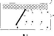
图1是按照本发明优选实施例设计的模块10的立面图。模块10包括上CSP12和下CSP14。每个CSP12和14具有上表面16和下表面18和相对侧面20和22。Figure 1 is an elevational view of a module 10 designed in accordance with a preferred embodiment of the present invention. Module 10 includes an
本发明使用多种类型和结构的CSP封装,例如管芯尺寸的和接近芯片尺寸的以及现有技术中公知的各种球栅阵列封装。这里这些将共同公知作为芯片尺寸封装集成电路(CSP),优选实施例将就CSP进行介绍,但是在示例图中使用的特定结构不作为限制。例如,图1和2的立面图描绘了本领域公知特定外形的CSP,应理解附图仅是示例性的。后面的附图示出本发明的实施例,其应用其它结构的CSP作为本发明可以应用的许多替换CSP结构另一个的实例。在从至少一个主表面发出可连接元件阵列技术中可用的广泛范围的CSP结构中使用本发明,产生了良好的效果。本发明有利地应用包含存储电路的CSP,而应用逻辑和计算电路产生了良好的效果,附加容量的同时不需要同量的PWB或其它板表面积消耗。The present invention utilizes various types and configurations of CSP packages, such as die-scale and near-chip-scale as well as various ball grid array packages known in the art. Here these will be collectively known as Chip Scale Package Integrated Circuits (CSPs) and preferred embodiments will be described in terms of CSPs, but the specific structures used in the example figures are not limiting. For example, the elevation views of FIGS. 1 and 2 depict CSPs of particular configurations known in the art, it being understood that the drawings are merely exemplary. The figures that follow illustrate embodiments of the invention that employ CSPs of other configurations as another example of the many alternative CSP configurations to which the invention can be applied. The invention is used to good effect in the wide range of CSP structures available in the technology of emitting arrays of connectable elements from at least one major surface. The present invention advantageously employs CSPs containing memory circuits, while applying logic and computation circuits yields good results, adding capacity without requiring the same amount of PWB or other board surface area consumption.
一般的CSP,例如球栅阵列(“BGA”)、微球栅阵列(“μBGA”)、和微间距球栅阵列(“FBGA”)封装具有可连接触点阵列,例如引线、焊点、焊球或以任意几种图形和间距从塑料壳的下表面18延伸的球。常常用焊球终止可连接触点的外部。图1示出沿着CSP12和14下表面18的CSP触点24。CSP触点24提供与在各个封装内的集成电路的连接。CSP触点24共同包括CSP阵列26,关于描绘的特定封装结构中的下CSP14示出了总体包括CSP阵列26的CSP阵列261和262。Typical CSP, such as ball grid array ("BGA"), micro ball grid array ("μBGA"), and fine pitch ball grid array ("FBGA") packages have an array of connectable contacts, such as leads, solder joints, solder The balls or balls extend from the
在图1中,示出了弯曲电路(“弯曲”、“弯曲电路”或“挠性电路结构”)30和32局部关于下CSP14卷绕,弯曲30在下CSP14的侧面20局部卷绕,弯曲32关于下CSP14的侧面22局部卷绕。侧面20和22可以充当面,或者如果CSP特别薄,可以充当端部。可以使用任何具有多层内层连接能力的挠性或合适的基板作为本发明的弯曲电路。整个弯曲电路可以是挠性的,或者本领域技术人员将认识到,可以应用在某个区域挠性制造的PCB结构(以在下CSP14周围具有整合性在沿着CSP表面用于可平面性的其它区域具有刚性)作为本发明弯曲电路的替代。例如,可以应用公知为硬柔的结构。In FIG. 1, flex circuits ("flex", "flex circuits" or "flex circuit structures") 30 and 32 are shown partially wrapped about the
部分弯曲电路30和32通过粘结剂34固定到下CSP14的上表面16,粘结剂34作为带粘结剂示出,可以是液体粘结剂或者可以放置在封装上分立位置中。粘结剂34优选为导热的。在模块10的装配中使用包括熔剂的粘结剂,产生了良好的效果。层34还可以是导热介质以促进模块10CSP之间的热流。Portions of
弯曲电路30和32可以是具有至少两层导电层的多层挠性电路结构。导电层优选是例如合金110的金属。将看到使用多层导电层提供了优点,本领域技术人员将认识到在模块10上建立分布电容来减小噪声或特别是在高频能够降低信号完整性的跳动效应。图1的模块10具有共同确定为模块阵列38的模块触点36。
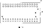
图2示出按照发明优选实施例设计的模块10。图2说明使用在优选实施例中设置的保形介质40以辅助建立模块10结构区域保形。通过保形介质40提高模块的可平面性。保形介质40优选为导热的。在另一实施例中,如参考标号41所示可以放置热散布机或者热介质。在图2中可以识别在弯曲电路30和32导电层之一处的上弯曲触点42和下弯曲触点44。上弯曲触点42和下弯曲触点44是导电材料,优选为固体金属。下弯曲触点44共同为下弯曲触点阵列46。上弯曲触点42共同为上弯曲触点阵列48。在图2中仅可以识别某些上弯曲触点42和下弯曲触点44以保持图的清晰。应理解每个弯曲电路30和32具有上弯曲触点42和下弯曲触点44。下弯曲触点44应用下CSP14,上弯曲触点42应用上CSP12。图2具有标记“A”的区域,其随后在图3中以放大图示出。Figure 2 shows a module 10 designed in accordance with a preferred embodiment of the invention. FIG. 2 illustrates the use of a conformal medium 40 provided in a preferred embodiment to assist in making the structural regions of the module 10 conformal. The planarity of the module is improved by the
图3以放大图描绘了图2中标记“A”的区域。图3说明实例CSP触点24和模块触点36之间通过下弯曲触点44的连接,从而说明从下CSP14到模块触点36的固体金属路径和由此到可连接模块的应用PWB的路径。本领域技术人员可以理解由此促进了从模块10的热转移。Figure 3 depicts the area marked "A" in Figure 2 in an enlarged view. Figure 3 illustrates the connection between the
继续参照图3,CSP触点24和模块触点36一起从应用平台例如PWB偏离模块10。CSP触点24和模块触点36的组合高度提供了比只有单个CSP触点24的高度长的矩臂。这提供了更长的矩臂,通过其能够分布随时间温度梯度应力(例如由温度循环代表)。With continued reference to FIG. 3 , the
在图3示出弯曲30包括多层。弯曲30具有第一外表面50和第二外表面52。弯曲电路30至少具有在第一和第二外表面50和52内部的两层导电层。在弯曲30和32种可以多于两层导电层。在所述优选实施例中,第一导电层54和第二导电层58在第一和第二外表面50和52的内部。在第一导电层54和第二导电层58之间存在中间层56。可以存在多于一层的中间层,而优选为一层聚酰亚胺中间层。In FIG. 3 the
如图3所绘并在随后附图中可以详细看出,在第二外表面52内部的第二导电层58层面处下弯曲触点44优选由金属构成。在优选实施例中,下弯曲触点44是固体金属并由例如合金110的金属合金构成。这产生了从下CSP14到应用板的固体金属通路,由此提供了用于分散在模块10中产生的热量的重要热通路。As depicted in FIG. 3 and seen in detail in subsequent figures, the
图4是实例CSP触点24和实例模块触点36之间通过下弯曲触点44示例连接的放大详图,从而说明从下CSP14到模块触点36的固体金属通路,和由此到可连接模块10的应用PWB的通路。如图4所示,下弯曲触点44在第二导电层58处,第二导电层58分别在弯曲电路30的第一和第二外表面层50和52的内部。4 is an enlarged detail view of an example connection between the
图5是在优选实施例中在下弯曲触点44周围示例区域的放大描绘。在第一和第二外表面层50和52中分别开口60和62,以提供到存在于弯曲中第二导电层58层面的特定下弯曲触点44的路径。通过上CSP12的CSP触点24接触上弯曲触点42。下弯曲触点44和上弯曲触点42是在弯曲中第二导电层58层面处导电材料(优选例如合金110的金属)的特定区域。在第二导电层58中区分上弯曲触点42和下弯曲触点44,如在随后的附图中所示,并且上弯曲触点42和下弯曲触点44可以与第二导电层8的导电平面连接或者与其隔离。通过在第二导电层58处示出的界限间隙63在图5中描述了与第二导电层58区分下弯曲触点44。在上或下弯曲触点42或44不与第二导电层58完全隔离的地方,界限间隙不像例如由随后的图12中的下弯曲触点44C所示的那样完全环绕弯曲触点延伸。下CSP14的CSP触点24穿过经第一外表面层50、第一导电层54和中间层56的开口60与适当的下弯曲触点44接触。穿过第二外表面层52开口62,模块触点36穿过第二外表面层52与适当的下弯曲触点44接触。FIG. 5 is an enlarged depiction of an example area around
在弯曲电路30和32种的第二导电层58层面处连接上CSP12和下CSP14的各个CSP触点24以使两个CSP的适当信号和电压触点互连。在弯曲电路30和32中第一导电层54层面处通过穿过中间层56的通孔来连接传输接地(VSS)信号的上CSP12和下CSP14的各个CSP触点24来连接个层面,随后将进一步详细说明结构。由此,连接CSP12和14。因此,当关于下CSP14放置弯曲电路30和32时,每个上和下CSP12和14的相应CSP触点24分别与上和下弯曲触点42和44接触。连接选定的上弯曲触点42和下弯曲触点44。因此,通过与下弯曲触点44接触,模块触点36与上和下CSP12和14接触。The
在优选实施例中,模块触点36穿过在第二外层52中的开口62与下CSP触点44接触。在某些实施例中,如随后所示,模块10将出现具有比模块10的组成CSP触点数多的模块触点阵列38。在这个实施例中,某些模块触点36可以与下弯曲触点44接触,下弯曲触点44不与下CSP14的CSP触点24之一接触而与上CSP12的CSP触点24连接。这使得模块10表达了比组成CSP12和14表达的宽的数据路径。模块触点36还可以与下弯曲触点44接触,从而提供一位置,通过该位置当没有得到未用的CSP触点或便于该目的实现时模块中CSP不同层面可被使能。In a preferred embodiment, the
在优选实施例中,第一导电层54用作接地平面,同时第二导电层58提供为信号传导层和电压传导层的功能。本领域技术人员将注意到,随着开口和等量互连中伴随的变化第一和第二导电层的功能可能相反。In a preferred embodiment, the first
本领域技术人员将认识到,上和下CSP12和14的相应电压CSP触点24的互连提供上和下CSP间的热通路以辅助缓和模块10中的热梯度。通过经第一导电层54上和下CSP12和14的常见接地CSP触点24的连接进而促进了横过模块10的热梯度曲线的这种变平。本领域技术人员将注意到,在第一和第二导电层54和58之间存在至少一层中间层56,在优选实施例中该中间层为聚酰亚胺。在导电接地第一导电层54和信号/电压导电第二导电层58之间放置这种中间层组合提供了分布电容,该分布电容辅助缓解接地跳动现象以提高模块10的高频性能。Those skilled in the art will recognize that the interconnection of the respective
在优选实施例中,图6描绘了弯曲30(即图1的左面)的第一外表面层50。该视图为从弯曲上从第一导电层54的透视图俯视到弯曲30。整个附图,位置标记“B”是对弯曲32以及横穿层弯曲层30的定向图。穿过第一外表面层50、第一导电层54和中间层56开口开口60。下CSP14的CSP触点24穿过第一外表面层50、第一导电层54和中间层56的开口60到达弯曲30的第二导电层58层面。在第二导电层58,下CSP14的选定的CSP触点24与选定的下弯曲触点44接触。如将参照随后的附图12所说明的那样下弯曲触点44在优选实施例中提供几种类型的连接。当装配模块10时,弯曲30的一部分将关于下CSP14的侧面20卷绕以在下CSP14的上表面16上放置端部62。In a preferred embodiment, FIG. 6 depicts the first
在优选实施例中,图7描绘了弯曲32(即图1的右面)的第一外表面层50。视图为从弯曲上从第一导电层54的透视图俯视到弯曲32。位置标记“B”相对图6和7的视图定向。观察图6和7可以理解每个视图的参考标记“B”放置得比同一层成对视图的另一观察任何角部彼此要近。如图7所示,穿过第一外表面层50、第一导电层54和中间层56开口开口60。下CSP14的CSP触点24穿过第一外表面层50、第一导电层54和中间层56的开口60到达弯曲30的第二导电层58的层面。在第二导电层58,下CSP14的选定的CSP触点24与下弯曲触点44接触。如将参照随后的附图12所说明的那样下弯曲触点44在优选实施例中提供几种类型的连接。当装配模块10时,弯曲32的一部分将关于下CSP14的侧面22卷绕以在下CSP14的上表面16上放置端部64。In a preferred embodiment, FIG. 7 depicts the first
图8描绘了弯曲30的第一导电层54。开口60继续弯曲30中的开孔,下CSP14的CSP触点通过该开口到达第二导电层58,由此到达在第二导电层58层面的选定的下弯曲触点44。FIG. 8 depicts the first
本领域技术人员将认识到因为弯曲30关于下CSP14的侧面20局部卷绕,在下CSP14的上表面16上设置的部分弯曲30上第一导电层54变成从上CSP12透视图的弯曲30的最下导电层。在所述实施例中,提供接地(VSS)连接的上CSP12的那些CSP触点24与第一导电层54连接。但是第一导电层54位于第二导电层58下面在下CSP14上卷绕的部分弯曲30,。因此,必须提供一些方法连接上弯曲触点42和第一导电层54,上CSP12的接地传输CSP触点24与该上弯曲触点42连接。因此,在所述优选实施例中,与上CSP12的接地传输CSP触点24接触的那些上弯曲触点42具有规定穿过中间层56到达第一导电层54路线的通孔。在图8中把那些与第一导电层54相遇的通孔的位置表示为通孔66。这些通孔可以是“焊盘上”或与其所连接的弯曲触点一致。本领域技术人员将注意到在图8中表示的通孔66和在所述优选实施例的第二导电层58的随后附图中表示的通孔66之间的匹配。在优选实施例中,在从图到图一致位置中的通孔66是一个通孔。为了简化视图,在附图中所绘通孔比制造实施例中直径上显示较大。本领域技术人员将认识到,可以通过通孔(在焊盘上或焊盘外),几种公知技术例如镀膜孔或固体线或布线的任意一种而不必是字面意思上的通孔,提供设置导电层之间的连接。Those skilled in the art will recognize that because the
在图8中还示出了焊盘外通孔74。在选定的开口60附近而不与其一致的位置在第一导电层54上设置焊盘外通孔74。与把选定上弯曲触点42和第一导电层54连接的通孔66不同,焊盘外通孔74使选定下弯曲触点44与第一导电层54连接。在上弯曲触点42附近,第二导电层58在通过上弯曲触点42(即上CSP12)与模块10连接的CSP和第一导电层54之间。因此,在接地传输上弯曲触点42和第一导电层54之间的通孔可以直接附着于选定的上弯曲触点42,接地信号通过选定的上弯曲触点42传输。相反,在下弯曲触点44附近,第一导电层54在通过下弯曲触点44(即下CSP14)与模块10连接的CSP和第二导电层58之间。因此,在接地传输下弯曲触点44和第一导电层54之间的通路通过在偏离位置所示的焊盘外通孔74偏离选定的下弯曲触点44。Also shown in FIG. 8 is an off-pad via 74 . An off-pad via 74 is provided on the first
图9说明弯曲32的第一导电层54。应用位置参考标记“B”相对定向图8和9。在图9中表示了开口60、通孔66和焊盘外通孔74。图9还示出了启动通孔68和70和启动轨迹72。启动通孔70使焊盘外在该优选实施例中与下CSP12(即N/C)的未用CSP触点对应的选定下弯曲触点44连接。在该位置的模块触点36把用于上CSP12的启动信号(C/S)通过选定的下弯曲触点44(其在第二导电层58的层面)传输到焊盘外启动通孔70,焊盘外启动通孔70把启动信号传输到第一导电层54由此传输到启动轨迹72。启动轨迹72进而把启动信号传输到启动通孔68,启动通孔68在用上CSP12的C/S引脚制造的触点处的第二导电层58层面通过中间层56延伸到选定的上弯曲触点42。由此,独立地启动了上和下CSP12和14。FIG. 9 illustrates the first
图10描绘了弯曲30的中间层56。在中间表面56中开口示出了开口60。下CSP14的CSP触点24穿过在中间层58中的开口60到达在第二导电层58层面的下弯曲触点44。本领域技术人员将注意到,在所述优选实施例中,开口60直径上比第一外层50中它们的表现要窄。通孔66、焊盘外通孔74和启动通孔68和70穿过中间层56,在第一和第二导电层54和58层面分别连接选定导电区域。图11描绘了弯曲32的中间层56,示出了开口60、通孔66、焊盘外通孔74和穿过中间层56的启动通孔68和70。FIG. 10 depicts the
图12描绘了本发明优选实施例的弯曲30的第二导电层58。描绘了多种类型的上弯曲触点42、各种类型的下弯曲触点44、信号轨迹76和VDD面78以及前面介绍的通孔66和焊盘外通孔74。整个附图12和13中,仅表示了示例特定特征以使附图清晰。弯曲触点44A用信号轨迹76与对应的选定上弯曲触点42A连接。为了增强附图的清晰度,在图12中仅照字面意思表示了示例的各个弯曲触点44A和42A。如所示的那样,在该优选实施例中,信号轨迹76表现通路路径,其在对应的弯曲触点42A和44A之间确定提供基本相等的信号长度。如所示的那样,轨迹76与表示为VDD面78的第二导电层58的较大表面区分离。VDD面78可以是一个或多个描绘的部分,优选为一个部分。下弯曲触点44C提供与VDD面78的连接。在优选实施例中,上弯曲触点42C和下弯曲触点44C分别使上CSP12和下CSP14与VDD面78连接。通过焊盘外通孔74与第一导电层54连接的下弯曲触点44表示为下弯曲触点44B。为了增强附图的清晰度,在图12中仅照字面意思表示了示例的各个下弯曲触点44B。通过通孔66与第一导电层54连接的上弯曲触点42表示为上弯曲触点42B。Figure 12 depicts the second
图13描绘了本发明优选实施例右侧弯曲32的第二导电层58。描绘了各种类型的上弯曲触点42、各种类型的下弯曲触点44、信号轨迹76和VDD面78以及前面介绍的通孔66、焊盘外74和启动通孔70和68。图13说明通过轨迹76与下弯曲触点44A连接的上弯曲触点42A。VDD面78在第二导电层58的层面提供了电压面。下弯曲触点44C和上弯曲触点42C分别使下CSP14和上CSP12与VDD面78连接。用在前介绍的启动通孔70示出下弯曲触点44D。对应的上弯曲触点42D通过启动通孔70和68与下弯曲触点44D连接,启动通孔70和68通过在弯曲32第一导电层54层面的在前介绍的启动轨迹72彼此连接。Figure 13 depicts the second
图14描绘了弯曲30的第二外层52。表示了开口62。本领域技术人员将认识到模块触点36穿过开口62与适当的下弯曲触点44接触。当弯曲30关于下CSP14的侧面20局部卷绕时,第二外层52的一部分变成自上CSP12透视图的弯曲30最上层。上CSP12的CSP触点24穿过开口64到达第二导电层58并与位于该层面的适当上弯曲触点42接触。图15反映了弯曲32的第二外层52并展现了开口64和62。模块触点36穿过开口62接触适当的下弯曲触点44。上CSP12的CSP触点24穿过开口64到达第二导电层58并与位于该层面的适当上弯曲触点42接触。FIG. 14 depicts the second
图16描绘了本发明的另一优选实施例,示出了模块10。本领域技术人员将认识到在图16中所述实施例与图12中的不同在于存在模块触点36E。模块触点36E提供了模块10数据路径的一部分并可以提供用于组成CSP不同启动的设备。在广泛数据路径供应中没有应用的模块触点36E可以提供接触点以提供启动信号来不同地启动上CSP12或下CSP14。FIG. 16 depicts another preferred embodiment of the invention, showing a module 10 . Those skilled in the art will recognize that the embodiment depicted in FIG. 16 differs from FIG. 12 in the presence of module contacts 36E. Module contact 36E provides a portion of the data path of module 10 and may provide facilities for various activations of the constituent CSP. Module contacts 36E, which are not used in extensive data path provisioning, may provide contact points to provide enable signals to enable
在广泛数据路径模块10中,组成上CSP12和下CSP14的数据路径的组合提供模块10,模块10表达为两个高模块10中组成CSP数据路径宽度两倍的模块数据路径。组合优选方法是相联系的,可以应用其它组合以组合在模块触点36和36E阵列上的CSP12和14的数据路径。In the broad data path module 10, the combination of the data paths making up the
作为实例,提供图17、18和19说明在本发明的替换实施例中使用添加的模块触点36E提供比在组成CSP12和14中存在的用于模块10的更宽数据路径。图17说明用于DDR-II FBGA封装的引脚输出。图18说明通过模块10的模块触点36和36E设置的引脚输出,表述了8位宽数据路径。按照本发明设计了模块10,在示例实施例中,模块10包括在定时中遵循DDR-II的上CSP12和下CSP14,其每个在数据路径中仅为4位宽。将认识到,在图18中所绘的模块10表达了8位宽数据路径。例如,图18描绘了在上CSP12(“顶”)和下CSP14(“底”)之间电源中不同的DQ引脚以聚集成8位。图19说明通过模块10的模块触点36和36E提供的引脚输出,表达了16位宽数据路径。模块10是按照本发明设计的,并且在该示例实施例中由在定时中遵循DDR-II的上CSP12和下CSP14构成,但其每个在数据路径中仅为8位。本领域技术人员将认识到宽度数据路径实施例可以应用在本领域中可得到的多种CSP的任意一种,并且这种CSP不需要为遵循DDR的。As an example, FIGS. 17 , 18 and 19 are provided to illustrate the use of added module contacts 36E in an alternate embodiment of the invention to provide a wider data path for module 10 than exists in
图20说明设置为CSP并且在本发明中可用的存储电路的一般引脚输出。由编号的列和照字母顺序的行的JEDEC惯例表示各个阵列位置。未占用中心区域(例如A3-A6;B3-B6等)。在按字母数字顺序表示的位置,例如如实例CSP触点24所示的A3,存在CSP触点24。图21描绘了在发明另一实施例中弯曲30的第二金属层58,其中模块10表达了比任一组成CSP12和14所表达宽的数据路径。下弯曲触点44E不接触下CSP14的CSP触点24,而是接触模块触点36E,从而用选定模块触点36提供了用于为2n位宽的模块10的数据路径,其中CSP12和14的数据路径具有n位宽度。如图21所示,下弯曲触点44E与上弯曲触点42E连接。如在前的图14所示,开口62穿过第二外层52。在图21中示出的第二导电层58的另一个优选实施例中,在弯曲电路30的第二外层52中模块触点36和36E穿过开口62与适当的下弯曲触点44接触。Figure 20 illustrates the general pin-outs of a memory circuit configured as CSP and usable in the present invention. Each array position is represented by the JEDEC convention of numbered columns and alphabetical rows. Unoccupied central area (eg A3-A6; B3-B6, etc.). At an alphanumeric position, such as A3 as shown for
图22说明在本发明另一实施例中的弯曲32的第二金属层58,其中模块10表达了比组成CSP12和14任一个所表达要宽的数据路径。下弯曲触点44E不接触下CSP14的CSP触点24,而是接触模块触点36E,从而用选定的模块触点36提供了用于为2n位宽的模块10的数据路径,其中CSP12和14的数据路径具有n位宽度。如图22所示,下弯曲触点44E与上弯曲触点42E连接。如在前的图14所示,开口62穿过第二外层52。在图22中示出的第二导电层58的另一个优选实施例中,模块触点36和36E穿过弯曲电路32的第二外层52中的开口62与适当的下弯曲触点44接触。FIG. 22 illustrates the
特别是在图21和22所述的实施例中,模块触点36E接触弯曲触点44E和44EE。本领域技术人员将认识到,在所述实施例中下弯曲触点44E数量为八(8),存在另一个在图21中示为参考标记44EE表示的下弯曲触点。通过模块触点36E之一接触下弯曲触点44EE以在上和下CSP之间提供不同启动。本领域技术人员将认识到下弯曲触点44E与对应的上弯曲触点42E连接。传输数据的上CSP12的CSP触点24与上弯曲触点42E接触。因此,组合上CSP12和下CSP14的数据路径在模块10上提供宽的数据路径。用图21和22所述的连接,弯曲电路30和32的下弯曲触点44E传输到模块触点36E、上CSP12的数据路径,同时其它下弯曲触点44把下CSP14的数据路径传输到模块触点36,从而提供给模块10上CSP12和下CSP14数据路径组合的模块数据路径。在图21和22所述的特定实施例中,模块10表达了16位数据路径,CSP12和CSP14每个表达了8位数据路径。In particular, in the embodiment depicted in FIGS. 21 and 22, module contact 36E contacts flex contacts 44E and 44EE. Those skilled in the art will recognize that, in the embodiment described, the number of lower flex contacts 44E is eight (8), there is another lower flex contact shown in FIG. 21 as indicated by reference numeral 44EE. The lower flex contact 44EE is contacted by one of the module contacts 36E to provide differential activation between the upper and lower CSPs. Those skilled in the art will recognize that the lower flex contacts 44E are connected to corresponding upper flex contacts 42E. The
虽然详细地介绍了本发明,本发明可以体现为多种具体形式对本领域技术人员是显而易见的,并且不脱离本发明的精神和范围可以做出各种变型、替代和变更。所介绍的实施例仅是说明性的而非限制性的,因此由所附权利要求表明发明的范围。Although the present invention has been described in detail, it will be obvious to those skilled in the art that the invention can be embodied in various specific forms, and that various changes, substitutions and alterations can be made therein without departing from the spirit and scope of the invention. The described embodiments are illustrative only and not restrictive, the scope of the invention being thus indicated by the appended claims.
Claims (42)
Translated fromChineseApplications Claiming Priority (2)
| Application Number | Priority Date | Filing Date | Title |
|---|---|---|---|
| US10/005,581 | 2001-10-26 | ||
| US10/005,581US6576992B1 (en) | 2001-10-26 | 2001-10-26 | Chip scale stacking system and method |
Related Child Applications (1)
| Application Number | Title | Priority Date | Filing Date |
|---|---|---|---|
| CN200810009614ADivisionCN100594608C (en) | 2001-10-26 | 2002-10-25 | High-density circuit module |
Publications (2)
| Publication Number | Publication Date |
|---|---|
| CN1608400Atrue CN1608400A (en) | 2005-04-20 |
| CN100449747C CN100449747C (en) | 2009-01-07 |
Family
ID=21716598
Family Applications (2)
| Application Number | Title | Priority Date | Filing Date |
|---|---|---|---|
| CN200810009614AExpired - LifetimeCN100594608C (en) | 2001-10-26 | 2002-10-25 | High-density circuit module |
| CNB028261879AExpired - LifetimeCN100449747C (en) | 2001-10-26 | 2002-10-25 | High Density Circuit Module |
Family Applications Before (1)
| Application Number | Title | Priority Date | Filing Date |
|---|---|---|---|
| CN200810009614AExpired - LifetimeCN100594608C (en) | 2001-10-26 | 2002-10-25 | High-density circuit module |
Country Status (4)
| Country | Link |
|---|---|
| US (4) | US6576992B1 (en) |
| CN (2) | CN100594608C (en) |
| GB (1) | GB2395367B (en) |
| WO (1) | WO2003037053A1 (en) |
Cited By (2)
| Publication number | Priority date | Publication date | Assignee | Title |
|---|---|---|---|---|
| CN103523739A (en)* | 2013-11-05 | 2014-01-22 | 华进半导体封装先导技术研发中心有限公司 | Packaging structure of three-dimensional flexible substrate of environment MEMS sensor and manufacturing method |
| CN103715184A (en)* | 2013-12-24 | 2014-04-09 | 华进半导体封装先导技术研发中心有限公司 | Three-dimensional multi-chip storage system packaging structure based on flexible base board and manufacturing method thereof |
Families Citing this family (105)
| Publication number | Priority date | Publication date | Assignee | Title |
|---|---|---|---|---|
| US6323060B1 (en) | 1999-05-05 | 2001-11-27 | Dense-Pac Microsystems, Inc. | Stackable flex circuit IC package and method of making same |
| US6262895B1 (en) | 2000-01-13 | 2001-07-17 | John A. Forthun | Stackable chip package with flex carrier |
| US6627984B2 (en)* | 2001-07-24 | 2003-09-30 | Dense-Pac Microsystems, Inc. | Chip stack with differing chip package types |
| DE10138278C1 (en)* | 2001-08-10 | 2003-04-03 | Infineon Technologies Ag | Electronic component with electronic components stacked on top of one another and method for producing the same |
| US6759745B2 (en)* | 2001-09-13 | 2004-07-06 | Texas Instruments Incorporated | Semiconductor device and manufacturing method thereof |
| US6940729B2 (en) | 2001-10-26 | 2005-09-06 | Staktek Group L.P. | Integrated circuit stacking system and method |
| US6956284B2 (en) | 2001-10-26 | 2005-10-18 | Staktek Group L.P. | Integrated circuit stacking system and method |
| US7371609B2 (en) | 2001-10-26 | 2008-05-13 | Staktek Group L.P. | Stacked module systems and methods |
| US7053478B2 (en) | 2001-10-26 | 2006-05-30 | Staktek Group L.P. | Pitch change and chip scale stacking system |
| US7202555B2 (en) | 2001-10-26 | 2007-04-10 | Staktek Group L.P. | Pitch change and chip scale stacking system and method |
| US20060255446A1 (en) | 2001-10-26 | 2006-11-16 | Staktek Group, L.P. | Stacked modules and method |
| US7026708B2 (en)* | 2001-10-26 | 2006-04-11 | Staktek Group L.P. | Low profile chip scale stacking system and method |
| US6914324B2 (en) | 2001-10-26 | 2005-07-05 | Staktek Group L.P. | Memory expansion and chip scale stacking system and method |
| US7310458B2 (en) | 2001-10-26 | 2007-12-18 | Staktek Group L.P. | Stacked module systems and methods |
| US7485951B2 (en) | 2001-10-26 | 2009-02-03 | Entorian Technologies, Lp | Modularized die stacking system and method |
| US20030234443A1 (en) | 2001-10-26 | 2003-12-25 | Staktek Group, L.P. | Low profile stacking system and method |
| US7656678B2 (en) | 2001-10-26 | 2010-02-02 | Entorian Technologies, Lp | Stacked module systems |
| US7081373B2 (en) | 2001-12-14 | 2006-07-25 | Staktek Group, L.P. | CSP chip stack with flex circuit |
| SG121707A1 (en)* | 2002-03-04 | 2006-05-26 | Micron Technology Inc | Method and apparatus for flip-chip packaging providing testing capability |
| SG111069A1 (en)* | 2002-06-18 | 2005-05-30 | Micron Technology Inc | Semiconductor devices including peripherally located bond pads, assemblies, packages, and methods |
| SG107595A1 (en) | 2002-06-18 | 2004-12-29 | Micron Technology Inc | Semiconductor devices and semiconductor device components with peripherally located, castellated contacts, assembles and packages including such semiconductor devices or packages and associated methods |
| KR100442880B1 (en) | 2002-07-24 | 2004-08-02 | 삼성전자주식회사 | Stacked semiconductor module and manufacturing method thereof |
| US20050167817A1 (en)* | 2002-08-05 | 2005-08-04 | Tessera, Inc. | Microelectronic adaptors, assemblies and methods |
| KR20040022063A (en)* | 2002-09-06 | 2004-03-11 | 주식회사 유니세미콘 | A stack semiconductor package and it's manufacture method |
| JP3867785B2 (en)* | 2002-10-15 | 2007-01-10 | セイコーエプソン株式会社 | Optical module |
| KR20040078807A (en)* | 2003-03-05 | 2004-09-13 | 삼성전자주식회사 | Ball Grid Array Stack Package |
| US6924551B2 (en)* | 2003-05-28 | 2005-08-02 | Intel Corporation | Through silicon via, folded flex microelectronic package |
| US6940158B2 (en)* | 2003-05-30 | 2005-09-06 | Tessera, Inc. | Assemblies having stacked semiconductor chips and methods of making same |
| US20040245615A1 (en)* | 2003-06-03 | 2004-12-09 | Staktek Group, L.P. | Point to point memory expansion system and method |
| KR100592786B1 (en)* | 2003-08-22 | 2006-06-26 | 삼성전자주식회사 | Laminated package and its manufacturing method using surface-mount semiconductor package |
| US7542304B2 (en) | 2003-09-15 | 2009-06-02 | Entorian Technologies, Lp | Memory expansion and integrated circuit stacking system and method |
| SG120123A1 (en)* | 2003-09-30 | 2006-03-28 | Micron Technology Inc | Castellated chip-scale packages and methods for fabricating the same |
| US20050150813A1 (en)* | 2003-10-29 | 2005-07-14 | Tessera, Inc. | Foldover packages and manufacturing and test methods therefor |
| US7126829B1 (en) | 2004-02-09 | 2006-10-24 | Pericom Semiconductor Corp. | Adapter board for stacking Ball-Grid-Array (BGA) chips |
| US7254036B2 (en)* | 2004-04-09 | 2007-08-07 | Netlist, Inc. | High density memory module using stacked printed circuit boards |
| WO2006016198A1 (en)* | 2004-08-02 | 2006-02-16 | Infineon Technologies Ag | Electronic component with stacked semiconductor chips and heat dissipating means |
| US20060050492A1 (en) | 2004-09-03 | 2006-03-09 | Staktek Group, L.P. | Thin module system and method |
| US20060053345A1 (en)* | 2004-09-03 | 2006-03-09 | Staktek Group L.P. | Thin module system and method |
| US7443023B2 (en) | 2004-09-03 | 2008-10-28 | Entorian Technologies, Lp | High capacity thin module system |
| US7606040B2 (en) | 2004-09-03 | 2009-10-20 | Entorian Technologies, Lp | Memory module system and method |
| US7468893B2 (en) | 2004-09-03 | 2008-12-23 | Entorian Technologies, Lp | Thin module system and method |
| US7289327B2 (en) | 2006-02-27 | 2007-10-30 | Stakick Group L.P. | Active cooling methods and apparatus for modules |
| US7606049B2 (en) | 2004-09-03 | 2009-10-20 | Entorian Technologies, Lp | Module thermal management system and method |
| US7446410B2 (en) | 2004-09-03 | 2008-11-04 | Entorian Technologies, Lp | Circuit module with thermal casing systems |
| US7423885B2 (en) | 2004-09-03 | 2008-09-09 | Entorian Technologies, Lp | Die module system |
| US7511968B2 (en)* | 2004-09-03 | 2009-03-31 | Entorian Technologies, Lp | Buffered thin module system and method |
| US7760513B2 (en) | 2004-09-03 | 2010-07-20 | Entorian Technologies Lp | Modified core for circuit module system and method |
| US7579687B2 (en)* | 2004-09-03 | 2009-08-25 | Entorian Technologies, Lp | Circuit module turbulence enhancement systems and methods |
| US7522421B2 (en) | 2004-09-03 | 2009-04-21 | Entorian Technologies, Lp | Split core circuit module |
| US7324352B2 (en)* | 2004-09-03 | 2008-01-29 | Staktek Group L.P. | High capacity thin module system and method |
| US7616452B2 (en)* | 2004-09-03 | 2009-11-10 | Entorian Technologies, Lp | Flex circuit constructions for high capacity circuit module systems and methods |
| US7542297B2 (en)* | 2004-09-03 | 2009-06-02 | Entorian Technologies, Lp | Optimized mounting area circuit module system and method |
| US7606050B2 (en) | 2004-09-03 | 2009-10-20 | Entorian Technologies, Lp | Compact module system and method |
| JP2006172586A (en)* | 2004-12-15 | 2006-06-29 | Hitachi Global Storage Technologies Netherlands Bv | Magnetic disk unit |
| US7309914B2 (en) | 2005-01-20 | 2007-12-18 | Staktek Group L.P. | Inverted CSP stacking system and method |
| US20060175694A1 (en)* | 2005-02-07 | 2006-08-10 | Hsin Chung H | Stacked structure of integrated circuits and method for manufacturing the same |
| US7291907B2 (en)* | 2005-02-28 | 2007-11-06 | Infineon Technologies, Ag | Chip stack employing a flex circuit |
| US20100020515A1 (en)* | 2005-03-08 | 2010-01-28 | Smart Modular Technologies, Inc. | Method and system for manufacturing micro solid state drive devices |
| US7098073B1 (en) | 2005-04-18 | 2006-08-29 | Freescale Semiconductor, Inc. | Method for stacking an integrated circuit on another integrated circuit |
| US7196427B2 (en)* | 2005-04-18 | 2007-03-27 | Freescale Semiconductor, Inc. | Structure having an integrated circuit on another integrated circuit with an intervening bent adhesive element |
| US20060255459A1 (en)* | 2005-05-11 | 2006-11-16 | Simon Muff | Stacked semiconductor memory device |
| US7033861B1 (en)* | 2005-05-18 | 2006-04-25 | Staktek Group L.P. | Stacked module systems and method |
| US7785928B2 (en) | 2005-07-09 | 2010-08-31 | Gautham Viswanadam | Integrated circuit device and method of manufacturing thereof |
| US7442050B1 (en) | 2005-08-29 | 2008-10-28 | Netlist, Inc. | Circuit card with flexible connection for memory module with heat spreader |
| US20070096333A1 (en)* | 2005-10-31 | 2007-05-03 | Amir Motamedi | Optimal stacked die organization |
| US7576995B2 (en)* | 2005-11-04 | 2009-08-18 | Entorian Technologies, Lp | Flex circuit apparatus and method for adding capacitance while conserving circuit board surface area |
| DE102005059189B3 (en)* | 2005-12-12 | 2007-03-08 | Infineon Technologies Ag | Arrangement of semiconductor memory devices for module, has conductive tracks connecting contacts of flexible substrate and stacked semiconductor devices |
| US7508069B2 (en) | 2006-01-11 | 2009-03-24 | Entorian Technologies, Lp | Managed memory component |
| US7508058B2 (en) | 2006-01-11 | 2009-03-24 | Entorian Technologies, Lp | Stacked integrated circuit module |
| US7608920B2 (en) | 2006-01-11 | 2009-10-27 | Entorian Technologies, Lp | Memory card and method for devising |
| US7304382B2 (en) | 2006-01-11 | 2007-12-04 | Staktek Group L.P. | Managed memory component |
| US7605454B2 (en) | 2006-01-11 | 2009-10-20 | Entorian Technologies, Lp | Memory card and method for devising |
| US20070164416A1 (en)* | 2006-01-17 | 2007-07-19 | James Douglas Wehrly | Managed memory component |
| US7511969B2 (en) | 2006-02-02 | 2009-03-31 | Entorian Technologies, Lp | Composite core circuit module system and method |
| US7619893B1 (en) | 2006-02-17 | 2009-11-17 | Netlist, Inc. | Heat spreader for electronic modules |
| SG135066A1 (en)* | 2006-02-20 | 2007-09-28 | Micron Technology Inc | Semiconductor device assemblies including face-to-face semiconductor dice, systems including such assemblies, and methods for fabricating such assemblies |
| US7888185B2 (en)* | 2006-08-17 | 2011-02-15 | Micron Technology, Inc. | Semiconductor device assemblies and systems including at least one conductive pathway extending around a side of at least one semiconductor device |
| US7868440B2 (en) | 2006-08-25 | 2011-01-11 | Micron Technology, Inc. | Packaged microdevices and methods for manufacturing packaged microdevices |
| US7425758B2 (en)* | 2006-08-28 | 2008-09-16 | Micron Technology, Inc. | Metal core foldover package structures |
| US7468553B2 (en) | 2006-10-20 | 2008-12-23 | Entorian Technologies, Lp | Stackable micropackages and stacked modules |
| US7417310B2 (en) | 2006-11-02 | 2008-08-26 | Entorian Technologies, Lp | Circuit module having force resistant construction |
| KR100829614B1 (en)* | 2006-12-29 | 2008-05-14 | 삼성전자주식회사 | Semiconductor stack package and manufacturing method thereof |
| US7508070B2 (en)* | 2007-01-13 | 2009-03-24 | Cheng-Lien Chiang | Two dimensional stacking using interposers |
| KR101065935B1 (en) | 2007-07-19 | 2011-09-19 | 엔이씨 액세스 테크니카 가부시키가이샤 | Electronic component mounting apparatus and manufacturing method thereof |
| EP2192613A4 (en)* | 2007-09-19 | 2011-03-16 | Nec Corp | Semiconductor device and its fabrication method |
| JP5115269B2 (en)* | 2008-03-26 | 2013-01-09 | 日本電気株式会社 | Semiconductor device mounting structure and electronic device using the mounting structure |
| US8018723B1 (en) | 2008-04-30 | 2011-09-13 | Netlist, Inc. | Heat dissipation for electronic modules |
| GB2459751A (en)* | 2008-05-06 | 2009-11-11 | Ibm | Self contained memory subsystem |
| US8466997B2 (en)* | 2009-12-31 | 2013-06-18 | Stmicroelectronics Pte Ltd. | Fan-out wafer level package for an optical sensor and method of manufacture thereof |
| US20110156240A1 (en)* | 2009-12-31 | 2011-06-30 | Stmicroelectronics Asia Pacific Pte. Ltd. | Reliable large die fan-out wafer level package and method of manufacture |
| US8884422B2 (en) | 2009-12-31 | 2014-11-11 | Stmicroelectronics Pte Ltd. | Flip-chip fan-out wafer level package for package-on-package applications, and method of manufacture |
| US8436255B2 (en)* | 2009-12-31 | 2013-05-07 | Stmicroelectronics Pte Ltd. | Fan-out wafer level package with polymeric layer for high reliability |
| US8502394B2 (en)* | 2009-12-31 | 2013-08-06 | Stmicroelectronics Pte Ltd. | Multi-stacked semiconductor dice scale package structure and method of manufacturing same |
| KR101796116B1 (en) | 2010-10-20 | 2017-11-10 | 삼성전자 주식회사 | Semiconductor device, memory module and memory system having the same and operating method thereof |
| US9013037B2 (en) | 2011-09-14 | 2015-04-21 | Stmicroelectronics Pte Ltd. | Semiconductor package with improved pillar bump process and structure |
| US8916481B2 (en) | 2011-11-02 | 2014-12-23 | Stmicroelectronics Pte Ltd. | Embedded wafer level package for 3D and package-on-package applications, and method of manufacture |
| US8779601B2 (en) | 2011-11-02 | 2014-07-15 | Stmicroelectronics Pte Ltd | Embedded wafer level package for 3D and package-on-package applications, and method of manufacture |
| US9888283B2 (en) | 2013-03-13 | 2018-02-06 | Nagrastar Llc | Systems and methods for performing transport I/O |
| USD758372S1 (en)* | 2013-03-13 | 2016-06-07 | Nagrastar Llc | Smart card interface |
| US9603252B1 (en)* | 2013-11-12 | 2017-03-21 | Smart Modular Technologies, Inc. | Integrated circuit device system with elevated configuration and method of manufacture thereof |
| US9648754B1 (en) | 2013-11-12 | 2017-05-09 | Smart Modular Technologies, Inc. | Integrated circuit device system with elevated stacked configuration and method of manufacture thereof |
| USD864968S1 (en) | 2015-04-30 | 2019-10-29 | Echostar Technologies L.L.C. | Smart card interface |
| CN111093316B (en)* | 2018-10-24 | 2021-08-24 | 鹏鼎控股(深圳)股份有限公司 | Circuit board and manufacturing method thereof |
| US11721657B2 (en) | 2019-06-14 | 2023-08-08 | Stmicroelectronics Pte Ltd | Wafer level chip scale package having varying thicknesses |
| CN113352069B (en)* | 2021-06-17 | 2022-06-28 | 江苏创源电子有限公司 | Workpiece feeding mechanism and workpiece assembling equipment |
Family Cites Families (217)
| Publication number | Priority date | Publication date | Assignee | Title |
|---|---|---|---|---|
| US150107A (en)* | 1874-04-21 | Improvement in machines for twisting auger-bits | ||
| US3294988A (en)* | 1964-09-24 | 1966-12-27 | Hewlett Packard Co | Transducers |
| US3372310A (en)* | 1965-04-30 | 1968-03-05 | Radiation Inc | Universal modular packages for integrated circuits |
| US3436604A (en) | 1966-04-25 | 1969-04-01 | Texas Instruments Inc | Complex integrated circuit array and method for fabricating same |
| US3654394A (en)* | 1969-07-08 | 1972-04-04 | Gordon Eng Co | Field effect transistor switch, particularly for multiplexing |
| US3772776A (en) | 1969-12-03 | 1973-11-20 | Thomas & Betts Corp | Method of interconnecting memory plane boards |
| US3727064A (en) | 1971-03-17 | 1973-04-10 | Monsanto Co | Opto-isolator devices and method for the fabrication thereof |
| US3746934A (en) | 1971-05-06 | 1973-07-17 | Siemens Ag | Stack arrangement of semiconductor chips |
| US3718842A (en)* | 1972-04-21 | 1973-02-27 | Texas Instruments Inc | Liquid crystal display mounting structure |
| US4079511A (en)* | 1976-07-30 | 1978-03-21 | Amp Incorporated | Method for packaging hermetically sealed integrated circuit chips on lead frames |
| US4103318A (en) | 1977-05-06 | 1978-07-25 | Ford Motor Company | Electronic multichip module |
| SU834957A1 (en) | 1979-03-12 | 1981-05-30 | Предприятие П/Я А-7438 | Device for feeding printed circuit boards |
| US4288841A (en) | 1979-09-20 | 1981-09-08 | Bell Telephone Laboratories, Incorporated | Double cavity semiconductor chip carrier |
| JPS5731166A (en) | 1980-07-31 | 1982-02-19 | Fujitsu Ltd | Semiconductor device |
| US4398235A (en) | 1980-09-11 | 1983-08-09 | General Motors Corporation | Vertical integrated circuit package integration |
| US4429349A (en)* | 1980-09-30 | 1984-01-31 | Burroughs Corporation | Coil connector |
| US4437235A (en) | 1980-12-29 | 1984-03-20 | Honeywell Information Systems Inc. | Integrated circuit package |
| US4513368A (en)* | 1981-05-22 | 1985-04-23 | Data General Corporation | Digital data processing system having object-based logical memory addressing and self-structuring modular memory |
| US4406508A (en) | 1981-07-02 | 1983-09-27 | Thomas & Betts Corporation | Dual-in-line package assembly |
| JPS5896756A (en) | 1981-12-04 | 1983-06-08 | Toshiba Corp | multi-chip package |
| JPS58112348A (en) | 1981-12-25 | 1983-07-04 | Fujitsu Ltd | semiconductor equipment |
| US4567543A (en)* | 1983-02-15 | 1986-01-28 | Motorola, Inc. | Double-sided flexible electronic circuit module |
| JPS59172253A (en) | 1983-03-18 | 1984-09-28 | Mitsubishi Electric Corp | semiconductor equipment |
| US4727513A (en)* | 1983-09-02 | 1988-02-23 | Wang Laboratories, Inc. | Signal in-line memory module |
| JPS6055458A (en)* | 1983-09-05 | 1985-03-30 | Matsushita Electric Ind Co Ltd | Cmos transistor circuit |
| KR890004820B1 (en) | 1984-03-28 | 1989-11-27 | 인터내셔널 비지네스 머신즈 코포레이션 | Memory module and board with double storage density and method of forming the same |
| US4587596A (en)* | 1984-04-09 | 1986-05-06 | Amp Incorporated | High density mother/daughter circuit board connector |
| JPS60254762A (en) | 1984-05-31 | 1985-12-16 | Fujitsu Ltd | Semiconductor device package |
| EP0213205B1 (en) | 1984-12-28 | 1992-12-09 | Micro Co., Ltd. | Method of stacking printed circuit boards |
| EP0218796B1 (en) | 1985-08-16 | 1990-10-31 | Dai-Ichi Seiko Co. Ltd. | Semiconductor device comprising a plug-in-type package |
| US4724611A (en)* | 1985-08-23 | 1988-02-16 | Nec Corporation | Method for producing semiconductor module |
| US4895703A (en)* | 1985-09-17 | 1990-01-23 | Calgon Corporation | Trihydroxybenzene boiler corrosion inhibitor compositions and method |
| US4696525A (en) | 1985-12-13 | 1987-09-29 | Amp Incorporated | Socket for stacking integrated circuit packages |
| US4722691A (en)* | 1986-02-03 | 1988-02-02 | General Motors Corporation | Header assembly for a printed circuit board |
| JPS62230027A (en) | 1986-03-31 | 1987-10-08 | Matsushita Electric Ind Co Ltd | Manufacture of semiconductor device |
| JPS62162891U (en)* | 1986-04-03 | 1987-10-16 | ||
| JPS63153849A (en) | 1986-12-17 | 1988-06-27 | Nec Corp | Semiconductor device |
| US4821007A (en) | 1987-02-06 | 1989-04-11 | Tektronix, Inc. | Strip line circuit component and method of manufacture |
| US4862249A (en) | 1987-04-17 | 1989-08-29 | Xoc Devices, Inc. | Packaging system for stacking integrated circuits |
| KR970003915B1 (en)* | 1987-06-24 | 1997-03-22 | 미다 가쓰시게 | Semiconductor memory device and semiconductor memory module using same |
| US4771366A (en) | 1987-07-06 | 1988-09-13 | International Business Machines Corporation | Ceramic card assembly having enhanced power distribution and cooling |
| IT1214254B (en) | 1987-09-23 | 1990-01-10 | Sgs Microelettonica S P A | SEMICONDUCTOR DEVICE IN PLASTIC OR CERAMIC CONTAINER WITH "CHIPS" FIXED ON BOTH SIDES OF THE CENTRAL ISLAND OF THE "FRAME". |
| US5016138A (en) | 1987-10-27 | 1991-05-14 | Woodman John K | Three dimensional integrated circuit package |
| US4983533A (en) | 1987-10-28 | 1991-01-08 | Irvine Sensors Corporation | High-density electronic modules - process and product |
| US5198888A (en) | 1987-12-28 | 1993-03-30 | Hitachi, Ltd. | Semiconductor stacked device |
| US4833568A (en) | 1988-01-29 | 1989-05-23 | Berhold G Mark | Three-dimensional circuit component assembly and method corresponding thereto |
| JP2600753B2 (en)* | 1988-02-03 | 1997-04-16 | 日本電気株式会社 | Input circuit |
| US4891789A (en) | 1988-03-03 | 1990-01-02 | Bull Hn Information Systems, Inc. | Surface mounted multilayer memory printed circuit board |
| US4992850A (en)* | 1989-02-15 | 1991-02-12 | Micron Technology, Inc. | Directly bonded simm module |
| US4911643A (en) | 1988-10-11 | 1990-03-27 | Beta Phase, Inc. | High density and high signal integrity connector |
| US4956694A (en) | 1988-11-04 | 1990-09-11 | Dense-Pac Microsystems, Inc. | Integrated circuit chip stacking |
| WO1990006609A1 (en)* | 1988-11-16 | 1990-06-14 | Motorola, Inc. | Flexible substrate electronic assembly |
| EP0382203B1 (en)* | 1989-02-10 | 1995-04-26 | Fujitsu Limited | Ceramic package type semiconductor device and method of assembling the same |
| US4992849A (en)* | 1989-02-15 | 1991-02-12 | Micron Technology, Inc. | Directly bonded board multiple integrated circuit module |
| US4953060A (en) | 1989-05-05 | 1990-08-28 | Ncr Corporation | Stackable integrated circuit chip package with improved heat removal |
| US5104820A (en) | 1989-07-07 | 1992-04-14 | Irvine Sensors Corporation | Method of fabricating electronic circuitry unit containing stacked IC layers having lead rerouting |
| US5012323A (en) | 1989-11-20 | 1991-04-30 | Micron Technology, Inc. | Double-die semiconductor package having a back-bonded die and a face-bonded die interconnected on a single leadframe |
| KR910011109A (en)* | 1989-11-28 | 1991-06-29 | 이헌조 | Insertion error of automatic part inserter |
| US5191404A (en)* | 1989-12-20 | 1993-03-02 | Digital Equipment Corporation | High density memory array packaging |
| JPH03227541A (en) | 1990-02-01 | 1991-10-08 | Hitachi Ltd | Semiconductor device |
| US5041015A (en) | 1990-03-30 | 1991-08-20 | Cal Flex, Inc. | Electrical jumper assembly |
| JP2816239B2 (en) | 1990-06-15 | 1998-10-27 | 株式会社日立製作所 | Resin-sealed semiconductor device |
| US5377077A (en) | 1990-08-01 | 1994-12-27 | Staktek Corporation | Ultra high density integrated circuit packages method and apparatus |
| US5475920A (en) | 1990-08-01 | 1995-12-19 | Burns; Carmen D. | Method of assembling ultra high density integrated circuit packages |
| EP0509065A1 (en) | 1990-08-01 | 1992-10-21 | Staktek Corporation | Ultra high density integrated circuit packages, method and apparatus |
| US5446620A (en) | 1990-08-01 | 1995-08-29 | Staktek Corporation | Ultra high density integrated circuit packages |
| US5499160A (en) | 1990-08-01 | 1996-03-12 | Staktek Corporation | High density integrated circuit module with snap-on rail assemblies |
| US5117282A (en)* | 1990-10-29 | 1992-05-26 | Harris Corporation | Stacked configuration for integrated circuit devices |
| JPH04209562A (en) | 1990-12-06 | 1992-07-30 | Fujitsu Ltd | Module structure of semiconductor package |
| US5289346A (en)* | 1991-02-26 | 1994-02-22 | Microelectronics And Computer Technology Corporation | Peripheral to area adapter with protective bumper for an integrated circuit chip |
| JPH04284661A (en) | 1991-03-13 | 1992-10-09 | Toshiba Corp | Semiconductor device |
| US5289062A (en)* | 1991-03-18 | 1994-02-22 | Quality Semiconductor, Inc. | Fast transmission gate switch |
| US5099393A (en) | 1991-03-25 | 1992-03-24 | International Business Machines Corporation | Electronic package for high density applications |
| US5138430A (en) | 1991-06-06 | 1992-08-11 | International Business Machines Corporation | High performance versatile thermally enhanced IC chip mounting |
| US5714802A (en)* | 1991-06-18 | 1998-02-03 | Micron Technology, Inc. | High-density electronic module |
| JPH0513666A (en) | 1991-06-29 | 1993-01-22 | Sony Corp | Complex semiconductor device |
| US5214307A (en)* | 1991-07-08 | 1993-05-25 | Micron Technology, Inc. | Lead frame for semiconductor devices having improved adhesive bond line control |
| US5311401A (en) | 1991-07-09 | 1994-05-10 | Hughes Aircraft Company | Stacked chip assembly and manufacturing method therefor |
| JP3014176B2 (en) | 1991-07-10 | 2000-02-28 | 新光電気工業株式会社 | Lead frame and semiconductor device |
| US5252857A (en)* | 1991-08-05 | 1993-10-12 | International Business Machines Corporation | Stacked DCA memory chips |
| US5448450A (en) | 1991-08-15 | 1995-09-05 | Staktek Corporation | Lead-on-chip integrated circuit apparatus |
| US5188926A (en)* | 1991-12-09 | 1993-02-23 | Eastman Kodak Company | Photographic elements having carbonamide coupler solvents and addenda to reduce sensitizing dye stain |
| US5397916A (en)* | 1991-12-10 | 1995-03-14 | Normington; Peter J. C. | Semiconductor device including stacked die |
| US5281852A (en) | 1991-12-10 | 1994-01-25 | Normington Peter J C | Semiconductor device including stacked die |
| US5198965A (en)* | 1991-12-18 | 1993-03-30 | International Business Machines Corporation | Free form packaging of specific functions within a computer system |
| US5241454A (en) | 1992-01-22 | 1993-08-31 | International Business Machines Corporation | Mutlilayered flexible circuit package |
| US5262927A (en) | 1992-02-07 | 1993-11-16 | Lsi Logic Corporation | Partially-molded, PCB chip carrier package |
| US5222014A (en) | 1992-03-02 | 1993-06-22 | Motorola, Inc. | Three-dimensional multi-chip pad array carrier |
| US5259770A (en) | 1992-03-19 | 1993-11-09 | Amp Incorporated | Impedance controlled elastomeric connector |
| US5438224A (en)* | 1992-04-23 | 1995-08-01 | Motorola, Inc. | Integrated circuit package having a face-to-face IC chip arrangement |
| US5247423A (en) | 1992-05-26 | 1993-09-21 | Motorola, Inc. | Stacking three dimensional leadless multi-chip module and method for making the same |
| US5702985A (en) | 1992-06-26 | 1997-12-30 | Staktek Corporation | Hermetically sealed ceramic integrated circuit heat dissipating package fabrication method |
| US5729894A (en)* | 1992-07-21 | 1998-03-24 | Lsi Logic Corporation | Method of assembling ball bump grid array semiconductor packages |
| US5266912A (en)* | 1992-08-19 | 1993-11-30 | Micron Technology, Inc. | Inherently impedance matched multiple integrated circuit module |
| JPH0679990A (en)* | 1992-09-04 | 1994-03-22 | Mitsubishi Electric Corp | Ic memory card |
| JP3105089B2 (en)* | 1992-09-11 | 2000-10-30 | 株式会社東芝 | Semiconductor device |
| US5731633A (en)* | 1992-09-16 | 1998-03-24 | Gary W. Hamilton | Thin multichip module |
| US5402006A (en) | 1992-11-10 | 1995-03-28 | Texas Instruments Incorporated | Semiconductor device with enhanced adhesion between heat spreader and leads and plastic mold compound |
| US5313097A (en) | 1992-11-16 | 1994-05-17 | International Business Machines, Corp. | High density memory module |
| US5375041A (en) | 1992-12-02 | 1994-12-20 | Intel Corporation | Ra-tab array bump tab tape based I.C. package |
| US5347428A (en) | 1992-12-03 | 1994-09-13 | Irvine Sensors Corporation | Module comprising IC memory stack dedicated to and structurally combined with an IC microprocessor chip |
| US5484959A (en) | 1992-12-11 | 1996-01-16 | Staktek Corporation | High density lead-on-package fabrication method and apparatus |
| US6205654B1 (en) | 1992-12-11 | 2001-03-27 | Staktek Group L.P. | Method of manufacturing a surface mount package |
| US5644161A (en) | 1993-03-29 | 1997-07-01 | Staktek Corporation | Ultra-high density warp-resistant memory module |
| US5801437A (en) | 1993-03-29 | 1998-09-01 | Staktek Corporation | Three-dimensional warp-resistant integrated circuit module method and apparatus |
| US5541812A (en) | 1995-05-22 | 1996-07-30 | Burns; Carmen D. | Bus communication system for stacked high density integrated circuit packages having an intermediate lead frame |
| US5455740A (en) | 1994-03-07 | 1995-10-03 | Staktek Corporation | Bus communication system for stacked high density integrated circuit packages |
| US5384690A (en)* | 1993-07-27 | 1995-01-24 | International Business Machines Corporation | Flex laminate package for a parallel processor |
| US5396573A (en)* | 1993-08-03 | 1995-03-07 | International Business Machines Corporation | Pluggable connectors for connecting large numbers of electrical and/or optical cables to a module through a seal |
| US5413970A (en)* | 1993-10-08 | 1995-05-09 | Texas Instruments Incorporated | Process for manufacturing a semiconductor package having two rows of interdigitated leads |
| US5386341A (en)* | 1993-11-01 | 1995-01-31 | Motorola, Inc. | Flexible substrate folded in a U-shape with a rigidizer plate located in the notch of the U-shape |
| US5523619A (en) | 1993-11-03 | 1996-06-04 | International Business Machines Corporation | High density memory structure |
| KR970000214B1 (en)* | 1993-11-18 | 1997-01-06 | 삼성전자 주식회사 | Semiconductor device and method of producing the same |
| US5477082A (en)* | 1994-01-11 | 1995-12-19 | Exponential Technology, Inc. | Bi-planar multi-chip module |
| US5502333A (en)* | 1994-03-30 | 1996-03-26 | International Business Machines Corporation | Semiconductor stack structures and fabrication/sparing methods utilizing programmable spare circuit |
| JPH07312469A (en)* | 1994-05-16 | 1995-11-28 | Nippon Mektron Ltd | Structure of bent part of multilayer flexible circuit board |
| US5592364A (en) | 1995-01-24 | 1997-01-07 | Staktek Corporation | High density integrated circuit module with complex electrical interconnect rails |
| US5491612A (en)* | 1995-02-21 | 1996-02-13 | Fairchild Space And Defense Corporation | Three-dimensional modular assembly of integrated circuits |
| US5514907A (en) | 1995-03-21 | 1996-05-07 | Simple Technology Incorporated | Apparatus for stacking semiconductor chips |
| US5612570A (en) | 1995-04-13 | 1997-03-18 | Dense-Pac Microsystems, Inc. | Chip stack and method of making same |
| JP2606177B2 (en)* | 1995-04-26 | 1997-04-30 | 日本電気株式会社 | Printed wiring board |
| DE19516272A1 (en) | 1995-05-08 | 1996-11-14 | Hermann Leguin | Primary element scanner for determining deflection of scanning pin or similar |
| US5872051A (en)* | 1995-08-02 | 1999-02-16 | International Business Machines Corporation | Process for transferring material to semiconductor chip conductive pads using a transfer substrate |
| US6025642A (en) | 1995-08-17 | 2000-02-15 | Staktek Corporation | Ultra high density integrated circuit packages |
| US5637920A (en)* | 1995-10-04 | 1997-06-10 | Lsi Logic Corporation | High contact density ball grid array package for flip-chips |
| US6013948A (en)* | 1995-11-27 | 2000-01-11 | Micron Technology, Inc. | Stackable chip scale semiconductor package with mating contacts on opposed surfaces |
| KR0184076B1 (en)* | 1995-11-28 | 1999-03-20 | 김광호 | Three-dimensional stacked package |
| US5646446A (en) | 1995-12-22 | 1997-07-08 | Fairchild Space And Defense Corporation | Three-dimensional flexible assembly of integrated circuits |
| JP3718008B2 (en)* | 1996-02-26 | 2005-11-16 | 株式会社日立製作所 | Memory module and manufacturing method thereof |
| JPH09260568A (en) | 1996-03-27 | 1997-10-03 | Mitsubishi Electric Corp | Semiconductor device and manufacturing method thereof |
| US5789815A (en)* | 1996-04-23 | 1998-08-04 | Motorola, Inc. | Three dimensional semiconductor package having flexible appendages |
| US5778522A (en)* | 1996-05-20 | 1998-07-14 | Staktek Corporation | Method of manufacturing a high density integrated circuit module with complex electrical interconnect rails having electrical interconnect strain relief |
| DE19626126C2 (en) | 1996-06-28 | 1998-04-16 | Fraunhofer Ges Forschung | Method for forming a spatial chip arrangement and spatial chip arrangement |
| US5822856A (en)* | 1996-06-28 | 1998-10-20 | International Business Machines Corporation | Manufacturing circuit board assemblies having filled vias |
| US6247228B1 (en)* | 1996-08-12 | 2001-06-19 | Tessera, Inc. | Electrical connection with inwardly deformable contacts |
| US6008538A (en)* | 1996-10-08 | 1999-12-28 | Micron Technology, Inc. | Method and apparatus providing redundancy for fabricating highly reliable memory modules |
| US6336262B1 (en)* | 1996-10-31 | 2002-01-08 | International Business Machines Corporation | Process of forming a capacitor with multi-level interconnection technology |
| JP3695893B2 (en)* | 1996-12-03 | 2005-09-14 | 沖電気工業株式会社 | Semiconductor device, manufacturing method and mounting method thereof |
| US6225688B1 (en)* | 1997-12-11 | 2001-05-01 | Tessera, Inc. | Stacked microelectronic assembly and method therefor |
| JP3455040B2 (en)* | 1996-12-16 | 2003-10-06 | 株式会社日立製作所 | Source clock synchronous memory system and memory unit |
| JPH10270506A (en)* | 1997-03-21 | 1998-10-09 | Mitsubishi Electric Corp | Semiconductor device |
| JP3011233B2 (en)* | 1997-05-02 | 2000-02-21 | 日本電気株式会社 | Semiconductor package and its semiconductor mounting structure |
| US6208521B1 (en) | 1997-05-19 | 2001-03-27 | Nitto Denko Corporation | Film carrier and laminate type mounting structure using same |
| US6028352A (en) | 1997-06-13 | 2000-02-22 | Irvine Sensors Corporation | IC stack utilizing secondary leadframes |
| US6014316A (en) | 1997-06-13 | 2000-01-11 | Irvine Sensors Corporation | IC stack utilizing BGA contacts |
| US5917709A (en)* | 1997-06-16 | 1999-06-29 | Eastman Kodak Company | Multiple circuit board assembly having an interconnect mechanism that includes a flex connector |
| US6040624A (en)* | 1997-10-02 | 2000-03-21 | Motorola, Inc. | Semiconductor device package and method |
| US6097087A (en)* | 1997-10-31 | 2000-08-01 | Micron Technology, Inc. | Semiconductor package including flex circuit, interconnects and dense array external contacts |
| US6205521B1 (en)* | 1997-11-03 | 2001-03-20 | Compaq Computer Corporation | Inclusion map for accelerated cache flush |
| US5869353A (en) | 1997-11-17 | 1999-02-09 | Dense-Pac Microsystems, Inc. | Modular panel stacking process |
| DE19754874A1 (en)* | 1997-12-10 | 1999-06-24 | Siemens Ag | Converting substrate with edge contacts into ball grid array |
| US6186106B1 (en)* | 1997-12-29 | 2001-02-13 | Visteon Global Technologies, Inc. | Apparatus for routing electrical signals in an engine |
| DE19758197C2 (en)* | 1997-12-30 | 2002-11-07 | Infineon Technologies Ag | Stack arrangement for two semiconductor memory chips and printed circuit board, which is equipped with a plurality of such stack arrangements |
| US5926369A (en) | 1998-01-22 | 1999-07-20 | International Business Machines Corporation | Vertically integrated multi-chip circuit package with heat-sink support |
| US6021048A (en)* | 1998-02-17 | 2000-02-01 | Smith; Gary W. | High speed memory module |
| US6028365A (en)* | 1998-03-30 | 2000-02-22 | Micron Technology, Inc. | Integrated circuit package and method of fabrication |
| US6172874B1 (en) | 1998-04-06 | 2001-01-09 | Silicon Graphics, Inc. | System for stacking of integrated circuit packages |
| US6180881B1 (en)* | 1998-05-05 | 2001-01-30 | Harlan Ruben Isaak | Chip stack and method of making same |
| US6329709B1 (en)* | 1998-05-11 | 2001-12-11 | Micron Technology, Inc. | Interconnections for a semiconductor device |
| US6300679B1 (en)* | 1998-06-01 | 2001-10-09 | Semiconductor Components Industries, Llc | Flexible substrate for packaging a semiconductor component |
| JP3186700B2 (en)* | 1998-06-24 | 2001-07-11 | 日本電気株式会社 | Semiconductor device and manufacturing method thereof |
| DE19833713C1 (en) | 1998-07-27 | 2000-05-04 | Siemens Ag | Laminate or stacked package arrangement based on at least two integrated circuits |
| US6153929A (en)* | 1998-08-21 | 2000-11-28 | Micron Technology, Inc. | Low profile multi-IC package connector |
| WO2000014802A1 (en)* | 1998-09-09 | 2000-03-16 | Seiko Epson Corporation | Semiconductor device, method of manufacture thereof, circuit board, and electronic device |
| US6187652B1 (en)* | 1998-09-14 | 2001-02-13 | Fujitsu Limited | Method of fabrication of multiple-layer high density substrate |
| US6347394B1 (en)* | 1998-11-04 | 2002-02-12 | Micron Technology, Inc. | Buffering circuit embedded in an integrated circuit device module used for buffering clocks and other input signals |
| US6239485B1 (en)* | 1998-11-13 | 2001-05-29 | Fujitsu Limited | Reduced cross-talk noise high density signal interposer with power and ground wrap |
| TW511723U (en)* | 1998-12-28 | 2002-11-21 | Foxconn Prec Components Co Ltd | Memory bus module |
| US6222737B1 (en)* | 1999-04-23 | 2001-04-24 | Dense-Pac Microsystems, Inc. | Universal package and method of forming the same |
| US6351029B1 (en)* | 1999-05-05 | 2002-02-26 | Harlan R. Isaak | Stackable flex circuit chip package and method of making same |
| US6323060B1 (en)* | 1999-05-05 | 2001-11-27 | Dense-Pac Microsystems, Inc. | Stackable flex circuit IC package and method of making same |
| JP2000353767A (en)* | 1999-05-14 | 2000-12-19 | Universal Instr Corp | Board for mounting electronic component, package, mounting method, and method for housing integrated circuit chip in package |
| US6376769B1 (en)* | 1999-05-18 | 2002-04-23 | Amerasia International Technology, Inc. | High-density electronic package, and method for making same |
| JP3526788B2 (en)* | 1999-07-01 | 2004-05-17 | 沖電気工業株式会社 | Method for manufacturing semiconductor device |
| US6370668B1 (en)* | 1999-07-23 | 2002-04-09 | Rambus Inc | High speed memory system capable of selectively operating in non-chip-kill and chip-kill modes |
| JP2001053243A (en)* | 1999-08-06 | 2001-02-23 | Hitachi Ltd | Semiconductor storage device and memory module |
| US6675469B1 (en)* | 1999-08-11 | 2004-01-13 | Tessera, Inc. | Vapor phase connection techniques |
| US6689634B1 (en)* | 1999-09-22 | 2004-02-10 | Texas Instruments Incorporated | Modeling technique for selectively depopulating electrical contacts from a foot print of a grid array (BGA or LGA) package to increase device reliability |
| KR100344927B1 (en)* | 1999-09-27 | 2002-07-19 | 삼성전자 주식회사 | Stack package and method for manufacturing the same |
| JP3633559B2 (en)* | 1999-10-01 | 2005-03-30 | セイコーエプソン株式会社 | Semiconductor device and manufacturing method thereof, circuit board, and electronic apparatus |
| US6441476B1 (en)* | 2000-10-18 | 2002-08-27 | Seiko Epson Corporation | Flexible tape carrier with external terminals formed on interposers |
| US6262895B1 (en) | 2000-01-13 | 2001-07-17 | John A. Forthun | Stackable chip package with flex carrier |
| US6489178B2 (en)* | 2000-01-26 | 2002-12-03 | Texas Instruments Incorporated | Method of fabricating a molded package for micromechanical devices |
| US6528870B2 (en)* | 2000-01-28 | 2003-03-04 | Kabushiki Kaisha Toshiba | Semiconductor device having a plurality of stacked wiring boards |
| JP2001223323A (en)* | 2000-02-10 | 2001-08-17 | Mitsubishi Electric Corp | Semiconductor device |
| TW579555B (en)* | 2000-03-13 | 2004-03-11 | Ibm | Semiconductor chip package and packaging of integrated circuit chip in electronic apparatus |
| JP3855594B2 (en)* | 2000-04-25 | 2006-12-13 | セイコーエプソン株式会社 | Semiconductor device |
| US6522018B1 (en)* | 2000-05-16 | 2003-02-18 | Micron Technology, Inc. | Ball grid array chip packages having improved testing and stacking characteristics |
| US20020006032A1 (en)* | 2000-05-23 | 2002-01-17 | Chris Karabatsos | Low-profile registered DIMM |
| US6683377B1 (en)* | 2000-05-30 | 2004-01-27 | Amkor Technology, Inc. | Multi-stacked memory package |
| US6560117B2 (en)* | 2000-06-28 | 2003-05-06 | Micron Technology, Inc. | Packaged microelectronic die assemblies and methods of manufacture |
| US6552910B1 (en)* | 2000-06-28 | 2003-04-22 | Micron Technology, Inc. | Stacked-die assemblies with a plurality of microelectronic devices and methods of manufacture |
| JP3390412B2 (en)* | 2000-08-07 | 2003-03-24 | 株式会社キャットアイ | head lamp |
| JP4397109B2 (en)* | 2000-08-14 | 2010-01-13 | 富士通株式会社 | Information processing apparatus and crossbar board unit / back panel assembly manufacturing method |
| US6349050B1 (en)* | 2000-10-10 | 2002-02-19 | Rambus, Inc. | Methods and systems for reducing heat flux in memory systems |
| US6884653B2 (en)* | 2001-03-21 | 2005-04-26 | Micron Technology, Inc. | Folded interposer |
| US6707684B1 (en)* | 2001-04-02 | 2004-03-16 | Advanced Micro Devices, Inc. | Method and apparatus for direct connection between two integrated circuits via a connector |
| DE10131939B4 (en)* | 2001-07-02 | 2014-12-11 | Qimonda Ag | Electronic circuit board with a plurality of housing-type housing semiconductor memories |
| JP2003031885A (en)* | 2001-07-19 | 2003-01-31 | Toshiba Corp | Semiconductor laser device |
| US6627984B2 (en)* | 2001-07-24 | 2003-09-30 | Dense-Pac Microsystems, Inc. | Chip stack with differing chip package types |
| US6451626B1 (en)* | 2001-07-27 | 2002-09-17 | Charles W.C. Lin | Three-dimensional stacked semiconductor package |
| JP2003045179A (en)* | 2001-08-01 | 2003-02-14 | Mitsubishi Electric Corp | Semiconductor element and semiconductor memory module using the same |
| JP2003059297A (en)* | 2001-08-08 | 2003-02-28 | Mitsubishi Electric Corp | Semiconductor storage device and semiconductor module using the same |
| US7605479B2 (en)* | 2001-08-22 | 2009-10-20 | Tessera, Inc. | Stacked chip assembly with encapsulant layer |
| US6927471B2 (en)* | 2001-09-07 | 2005-08-09 | Peter C. Salmon | Electronic system modules and method of fabrication |
| US6977440B2 (en)* | 2001-10-09 | 2005-12-20 | Tessera, Inc. | Stacked packages |
| KR20030029743A (en)* | 2001-10-10 | 2003-04-16 | 삼성전자주식회사 | Stack package using flexible double wiring substrate |
| US20030234443A1 (en)* | 2001-10-26 | 2003-12-25 | Staktek Group, L.P. | Low profile stacking system and method |
| US6914324B2 (en)* | 2001-10-26 | 2005-07-05 | Staktek Group L.P. | Memory expansion and chip scale stacking system and method |
| TW565918B (en)* | 2002-07-03 | 2003-12-11 | United Test Ct Inc | Semiconductor package with heat sink |
| JP2004055009A (en)* | 2002-07-18 | 2004-02-19 | Renesas Technology Corp | Semiconductor memory module |
| US6765288B2 (en)* | 2002-08-05 | 2004-07-20 | Tessera, Inc. | Microelectronic adaptors, assemblies and methods |
| JP4085788B2 (en)* | 2002-08-30 | 2008-05-14 | 日本電気株式会社 | SEMICONDUCTOR DEVICE AND ITS MANUFACTURING METHOD, CIRCUIT BOARD, ELECTRONIC DEVICE |
| US6838761B2 (en)* | 2002-09-17 | 2005-01-04 | Chippac, Inc. | Semiconductor multi-package module having wire bond interconnect between stacked packages and having electrical shield |
| US6841855B2 (en)* | 2003-04-28 | 2005-01-11 | Intel Corporation | Electronic package having a flexible substrate with ends connected to one another |
| KR100592786B1 (en)* | 2003-08-22 | 2006-06-26 | 삼성전자주식회사 | Laminated package and its manufacturing method using surface-mount semiconductor package |
| US20050018495A1 (en)* | 2004-01-29 | 2005-01-27 | Netlist, Inc. | Arrangement of integrated circuits in a memory module |
- 2001
- 2001-10-26USUS10/005,581patent/US6576992B1/ennot_activeExpired - Lifetime
- 2002
- 2002-10-25CNCN200810009614Apatent/CN100594608C/ennot_activeExpired - Lifetime
- 2002-10-25GBGB0406140Apatent/GB2395367B/ennot_activeExpired - Fee Related
- 2002-10-25CNCNB028261879Apatent/CN100449747C/ennot_activeExpired - Lifetime
- 2002-10-25WOPCT/US2002/034340patent/WO2003037053A1/ennot_activeApplication Discontinuation
- 2003
- 2003-03-27USUS10/400,309patent/US20030137048A1/ennot_activeAbandoned
- 2005
- 2005-12-21USUS11/316,505patent/US20060091521A1/ennot_activeAbandoned
- 2005-12-22USUS11/317,425patent/US20060131716A1/ennot_activeAbandoned
Cited By (2)
| Publication number | Priority date | Publication date | Assignee | Title |
|---|---|---|---|---|
| CN103523739A (en)* | 2013-11-05 | 2014-01-22 | 华进半导体封装先导技术研发中心有限公司 | Packaging structure of three-dimensional flexible substrate of environment MEMS sensor and manufacturing method |
| CN103715184A (en)* | 2013-12-24 | 2014-04-09 | 华进半导体封装先导技术研发中心有限公司 | Three-dimensional multi-chip storage system packaging structure based on flexible base board and manufacturing method thereof |
Also Published As
| Publication number | Publication date |
|---|---|
| GB2395367B (en) | 2005-05-25 |
| US20030137048A1 (en) | 2003-07-24 |
| HK1077460A1 (en) | 2006-02-10 |
| CN100594608C (en) | 2010-03-17 |
| US6576992B1 (en) | 2003-06-10 |
| US20060131716A1 (en) | 2006-06-22 |
| GB0406140D0 (en) | 2004-04-21 |
| CN100449747C (en) | 2009-01-07 |
| GB2395367A (en) | 2004-05-19 |
| CN101271886A (en) | 2008-09-24 |
| WO2003037053A1 (en) | 2003-05-01 |
| US20060091521A1 (en) | 2006-05-04 |
Similar Documents
| Publication | Publication Date | Title |
|---|---|---|
| CN1608400A (en) | Chip scale stacking system and method | |
| CN1282244C (en) | Electronic module with three-dimensional array of carrier-mounted integrated circuit packages | |
| US7495334B2 (en) | Stacking system and method | |
| US7595550B2 (en) | Flex-based circuit module | |
| TWI389273B (en) | Semiconductor die assembly | |
| US8786069B1 (en) | Reconfigurable pop | |
| US20080079132A1 (en) | Inverted CSP Stacking System and Method | |
| JP2008263197A (en) | Circuit board assembly having semiconductor chip, electric assembly using the circuit board assembly, and information processing system using the electric assembly | |
| KR20140123577A (en) | Three dimensional passive multi-component structures | |
| JP3610661B2 (en) | Three-dimensional laminated module | |
| CN1728918A (en) | Circuitized substrate | |
| US20060055024A1 (en) | Adapted leaded integrated circuit module | |
| CN1971894A (en) | Chip-embedded modular structure | |
| US20070284717A1 (en) | Device embedded with semiconductor chip and stack structure of the same | |
| CN101209003A (en) | High capacity thin module system and method | |
| CN101465341B (en) | Stacked Chip Package Structure | |
| US6965169B2 (en) | Hybrid integrated circuit package substrate | |
| US7679201B2 (en) | Device package | |
| HK1077460B (en) | A high-density circuit module | |
| CN1971904A (en) | The stacked structure of semiconductor components embedded in the carrier board | |
| US20050146011A1 (en) | Pitch change and chip scale stacking system and method | |
| CN120261444A (en) | Semiconductor Package | |
| JPH11354671A (en) | Semiconductor package | |
| HK1103475A (en) | Integrated circuit stacking system and method |
Legal Events
| Date | Code | Title | Description |
|---|---|---|---|
| C06 | Publication | ||
| PB01 | Publication | ||
| C10 | Entry into substantive examination | ||
| SE01 | Entry into force of request for substantive examination | ||
| REG | Reference to a national code | Ref country code:HK Ref legal event code:DE Ref document number:1077460 Country of ref document:HK | |
| C14 | Grant of patent or utility model | ||
| GR01 | Patent grant | ||
| REG | Reference to a national code | Ref country code:HK Ref legal event code:GR Ref document number:1077460 Country of ref document:HK | |
| ASS | Succession or assignment of patent right | Owner name:OVD DATA LLC Free format text:FORMER OWNER: YINTAORUN TECHNOLOGY CO., LTD. Effective date:20130329 | |
| C41 | Transfer of patent application or patent right or utility model | ||
| C56 | Change in the name or address of the patentee | Owner name:YINTAORUN TECHNOLOGY CO., LTD. Free format text:FORMER NAME: STAKTEK GROUP L. P. | |
| CP01 | Change in the name or title of a patent holder | Address after:Texas, USA Patentee after:Printing Technology Corp. Address before:Texas, USA Patentee before:Entorian Technologies, L.P. | |
| TR01 | Transfer of patent right | Effective date of registration:20130329 Address after:Delaware Patentee after:Data LLC Address before:Texas, USA Patentee before:Printing Technology Corp. | |
| CX01 | Expiry of patent term | Granted publication date:20090107 | |
| CX01 | Expiry of patent term |