CN1606391A - El display device, driving method thereof, and electronic equipment provided with the display device - Google Patents
El display device, driving method thereof, and electronic equipment provided with the display deviceDownload PDFInfo
- Publication number
- CN1606391A CN1606391ACNA2004100880718ACN200410088071ACN1606391ACN 1606391 ACN1606391 ACN 1606391ACN A2004100880718 ACNA2004100880718 ACN A2004100880718ACN 200410088071 ACN200410088071 ACN 200410088071ACN 1606391 ACN1606391 ACN 1606391A
- Authority
- CN
- China
- Prior art keywords
- formed over
- film
- display device
- insulating film
- tft
- Prior art date
- Legal status (The legal status is an assumption and is not a legal conclusion. Google has not performed a legal analysis and makes no representation as to the accuracy of the status listed.)
- Granted
Links
- 238000000034methodMethods0.000titleabstractdescription85
- 239000010408filmSubstances0.000claimsdescription283
- 239000000758substrateSubstances0.000claimsdescription41
- 239000000463materialSubstances0.000claimsdescription40
- 238000002161passivationMethods0.000claimsdescription36
- 230000001681protective effectEffects0.000claimsdescription12
- 239000010409thin filmSubstances0.000claimsdescription8
- 229910052710siliconInorganic materials0.000abstractdescription38
- XUIMIQQOPSSXEZ-UHFFFAOYSA-NSiliconChemical compound[Si]XUIMIQQOPSSXEZ-UHFFFAOYSA-N0.000abstractdescription37
- 239000010703siliconSubstances0.000abstractdescription37
- 239000013078crystalSubstances0.000abstractdescription22
- 238000005401electroluminescenceMethods0.000description172
- 239000010410layerSubstances0.000description111
- 239000011229interlayerSubstances0.000description35
- 239000012535impuritySubstances0.000description31
- 239000011159matrix materialSubstances0.000description24
- 230000008569processEffects0.000description24
- OAICVXFJPJFONN-UHFFFAOYSA-NPhosphorusChemical compound[P]OAICVXFJPJFONN-UHFFFAOYSA-N0.000description17
- VYPSYNLAJGMNEJ-UHFFFAOYSA-Nsilicon dioxideInorganic materialsO=[Si]=OVYPSYNLAJGMNEJ-UHFFFAOYSA-N0.000description16
- 238000010894electron beam technologyMethods0.000description15
- 238000010438heat treatmentMethods0.000description15
- 229910052698phosphorusInorganic materials0.000description14
- 239000011574phosphorusSubstances0.000description14
- IJGRMHOSHXDMSA-UHFFFAOYSA-NAtomic nitrogenChemical compoundN#NIJGRMHOSHXDMSA-UHFFFAOYSA-N0.000description13
- 229910052581Si3N4Inorganic materials0.000description13
- 230000015572biosynthetic processEffects0.000description13
- 238000004519manufacturing processMethods0.000description13
- 229910021420polycrystalline siliconInorganic materials0.000description13
- 229920005591polysiliconPolymers0.000description13
- HQVNEWCFYHHQES-UHFFFAOYSA-Nsilicon nitrideChemical compoundN12[Si]34N5[Si]62N3[Si]51N64HQVNEWCFYHHQES-UHFFFAOYSA-N0.000description13
- 239000002585baseSubstances0.000description12
- 229910052782aluminiumInorganic materials0.000description11
- 230000000694effectsEffects0.000description11
- 238000002347injectionMethods0.000description11
- 239000007924injectionSubstances0.000description11
- PXHVJJICTQNCMI-UHFFFAOYSA-NnickelSubstances[Ni]PXHVJJICTQNCMI-UHFFFAOYSA-N0.000description11
- 229910052814silicon oxideInorganic materials0.000description11
- XAGFODPZIPBFFR-UHFFFAOYSA-NaluminiumChemical compound[Al]XAGFODPZIPBFFR-UHFFFAOYSA-N0.000description10
- 239000004065semiconductorSubstances0.000description10
- ZOXJGFHDIHLPTG-UHFFFAOYSA-NBoronChemical compound[B]ZOXJGFHDIHLPTG-UHFFFAOYSA-N0.000description9
- 229910052796boronInorganic materials0.000description9
- 239000011521glassSubstances0.000description9
- 229920005989resinPolymers0.000description9
- 239000011347resinSubstances0.000description9
- 238000001994activationMethods0.000description8
- 239000003990capacitorSubstances0.000description8
- 238000001816coolingMethods0.000description8
- XLYOFNOQVPJJNP-UHFFFAOYSA-NwaterSubstancesOXLYOFNOQVPJJNP-UHFFFAOYSA-N0.000description8
- 230000004913activationEffects0.000description7
- 229910052783alkali metalInorganic materials0.000description7
- 150000001340alkali metalsChemical class0.000description7
- 239000007789gasSubstances0.000description7
- 229910052757nitrogenInorganic materials0.000description7
- 230000003071parasitic effectEffects0.000description7
- 239000010936titaniumSubstances0.000description7
- -1tungsten nitrideChemical class0.000description7
- UFHFLCQGNIYNRP-UHFFFAOYSA-NHydrogenChemical compound[H][H]UFHFLCQGNIYNRP-UHFFFAOYSA-N0.000description6
- 239000001257hydrogenSubstances0.000description6
- 229910052739hydrogenInorganic materials0.000description6
- 239000011261inert gasSubstances0.000description6
- 150000002500ionsChemical class0.000description6
- 238000004020luminiscence typeMethods0.000description6
- 229910052751metalInorganic materials0.000description6
- 239000002184metalSubstances0.000description6
- 230000003647oxidationEffects0.000description6
- 238000007254oxidation reactionMethods0.000description6
- 229910052721tungstenInorganic materials0.000description6
- 239000010937tungstenSubstances0.000description6
- 229910021417amorphous siliconInorganic materials0.000description5
- 238000001354calcinationMethods0.000description5
- 239000000969carrierSubstances0.000description5
- 239000010949copperSubstances0.000description5
- 230000007547defectEffects0.000description5
- 230000005525hole transportEffects0.000description5
- 238000005984hydrogenation reactionMethods0.000description5
- 239000010453quartzSubstances0.000description5
- 239000002356single layerSubstances0.000description5
- 238000004544sputter depositionMethods0.000description5
- 238000001771vacuum depositionMethods0.000description5
- RYGMFSIKBFXOCR-UHFFFAOYSA-NCopperChemical compound[Cu]RYGMFSIKBFXOCR-UHFFFAOYSA-N0.000description4
- 239000012790adhesive layerSubstances0.000description4
- 229910045601alloyInorganic materials0.000description4
- 239000000956alloySubstances0.000description4
- QVQLCTNNEUAWMS-UHFFFAOYSA-Nbarium oxideChemical compound[Ba]=OQVQLCTNNEUAWMS-UHFFFAOYSA-N0.000description4
- UMIVXZPTRXBADB-UHFFFAOYSA-NbenzocyclobuteneChemical compoundC1=CC=C2CCC2=C1UMIVXZPTRXBADB-UHFFFAOYSA-N0.000description4
- 229910052802copperInorganic materials0.000description4
- 230000007423decreaseEffects0.000description4
- 239000002274desiccantSubstances0.000description4
- 239000007788liquidSubstances0.000description4
- 239000011777magnesiumSubstances0.000description4
- 238000005259measurementMethods0.000description4
- 229910021421monocrystalline siliconInorganic materials0.000description4
- 238000000926separation methodMethods0.000description4
- WFKWXMTUELFFGS-UHFFFAOYSA-NtungstenChemical compound[W]WFKWXMTUELFFGS-UHFFFAOYSA-N0.000description4
- 235000012431wafersNutrition0.000description4
- 239000004743PolypropyleneSubstances0.000description3
- RTAQQCXQSZGOHL-UHFFFAOYSA-NTitaniumChemical compound[Ti]RTAQQCXQSZGOHL-UHFFFAOYSA-N0.000description3
- XLOMVQKBTHCTTD-UHFFFAOYSA-NZinc monoxideChemical compound[Zn]=OXLOMVQKBTHCTTD-UHFFFAOYSA-N0.000description3
- 238000004458analytical methodMethods0.000description3
- 238000000137annealingMethods0.000description3
- QVGXLLKOCUKJST-UHFFFAOYSA-Natomic oxygenChemical compound[O]QVGXLLKOCUKJST-UHFFFAOYSA-N0.000description3
- 230000015556catabolic processEffects0.000description3
- 239000003054catalystSubstances0.000description3
- 239000011651chromiumSubstances0.000description3
- 238000006731degradation reactionMethods0.000description3
- 230000006866deteriorationEffects0.000description3
- 238000010586diagramMethods0.000description3
- 230000005669field effectEffects0.000description3
- 230000001590oxidative effectEffects0.000description3
- 229910052760oxygenInorganic materials0.000description3
- 239000001301oxygenSubstances0.000description3
- 238000005268plasma chemical vapour depositionMethods0.000description3
- 229920001155polypropylenePolymers0.000description3
- 230000009467reductionEffects0.000description3
- 238000001004secondary ion mass spectrometryMethods0.000description3
- HBMJWWWQQXIZIP-UHFFFAOYSA-Nsilicon carbideChemical compound[Si+]#[C-]HBMJWWWQQXIZIP-UHFFFAOYSA-N0.000description3
- 229910010271silicon carbideInorganic materials0.000description3
- 229910052719titaniumInorganic materials0.000description3
- 239000004925Acrylic resinSubstances0.000description2
- 229920000178Acrylic resinPolymers0.000description2
- XKRFYHLGVUSROY-UHFFFAOYSA-NArgonChemical compound[Ar]XKRFYHLGVUSROY-UHFFFAOYSA-N0.000description2
- 229910052582BNInorganic materials0.000description2
- PZNSFCLAULLKQX-UHFFFAOYSA-NBoron nitrideChemical compoundN#BPZNSFCLAULLKQX-UHFFFAOYSA-N0.000description2
- VYZAMTAEIAYCRO-UHFFFAOYSA-NChromiumChemical compound[Cr]VYZAMTAEIAYCRO-UHFFFAOYSA-N0.000description2
- MYMOFIZGZYHOMD-UHFFFAOYSA-NDioxygenChemical compoundO=OMYMOFIZGZYHOMD-UHFFFAOYSA-N0.000description2
- ZOKXTWBITQBERF-UHFFFAOYSA-NMolybdenumChemical compound[Mo]ZOKXTWBITQBERF-UHFFFAOYSA-N0.000description2
- XYFCBTPGUUZFHI-UHFFFAOYSA-NPhosphineChemical compoundPXYFCBTPGUUZFHI-UHFFFAOYSA-N0.000description2
- 239000004642PolyimideSubstances0.000description2
- PPBRXRYQALVLMV-UHFFFAOYSA-NStyreneChemical compoundC=CC1=CC=CC=C1PPBRXRYQALVLMV-UHFFFAOYSA-N0.000description2
- NRTOMJZYCJJWKI-UHFFFAOYSA-NTitanium nitrideChemical compound[Ti]#NNRTOMJZYCJJWKI-UHFFFAOYSA-N0.000description2
- 239000000853adhesiveSubstances0.000description2
- 230000001070adhesive effectEffects0.000description2
- 230000005540biological transmissionEffects0.000description2
- FFBGYFUYJVKRNV-UHFFFAOYSA-NboranylidynephosphaneChemical compoundP#BFFBGYFUYJVKRNV-UHFFFAOYSA-N0.000description2
- 239000011575calciumSubstances0.000description2
- 239000000919ceramicSubstances0.000description2
- 230000008859changeEffects0.000description2
- 229910052804chromiumInorganic materials0.000description2
- PMHQVHHXPFUNSP-UHFFFAOYSA-Mcopper(1+);methylsulfanylmethane;bromideChemical compoundBr[Cu].CSCPMHQVHHXPFUNSP-UHFFFAOYSA-M0.000description2
- 229910003460diamondInorganic materials0.000description2
- 239000010432diamondSubstances0.000description2
- ZOCHARZZJNPSEU-UHFFFAOYSA-NdiboronChemical compoundB#BZOCHARZZJNPSEU-UHFFFAOYSA-N0.000description2
- 229910001882dioxygenInorganic materials0.000description2
- 239000003822epoxy resinSubstances0.000description2
- 230000005284excitationEffects0.000description2
- 230000006870functionEffects0.000description2
- 230000007274generation of a signal involved in cell-cell signalingEffects0.000description2
- 238000002173high-resolution transmission electron microscopyMethods0.000description2
- 229910003437indium oxideInorganic materials0.000description2
- PJXISJQVUVHSOJ-UHFFFAOYSA-Nindium(iii) oxideChemical compound[O-2].[O-2].[O-2].[In+3].[In+3]PJXISJQVUVHSOJ-UHFFFAOYSA-N0.000description2
- 238000005468ion implantationMethods0.000description2
- 239000005355lead glassSubstances0.000description2
- 239000004973liquid crystal related substanceSubstances0.000description2
- 229910052749magnesiumInorganic materials0.000description2
- 229910052750molybdenumInorganic materials0.000description2
- 239000011733molybdenumSubstances0.000description2
- 229910052754neonInorganic materials0.000description2
- 239000011368organic materialSubstances0.000description2
- 230000010355oscillationEffects0.000description2
- TWNQGVIAIRXVLR-UHFFFAOYSA-Noxo(oxoalumanyloxy)alumaneChemical compoundO=[Al]O[Al]=OTWNQGVIAIRXVLR-UHFFFAOYSA-N0.000description2
- 238000000059patterningMethods0.000description2
- 238000000206photolithographyMethods0.000description2
- 229920000647polyepoxidePolymers0.000description2
- 229920001721polyimidePolymers0.000description2
- 239000011241protective layerSubstances0.000description2
- 229910052709silverInorganic materials0.000description2
- 239000000243solutionSubstances0.000description2
- 238000003860storageMethods0.000description2
- NIXOWILDQLNWCW-UHFFFAOYSA-MAcrylateChemical compound[O-]C(=O)C=CNIXOWILDQLNWCW-UHFFFAOYSA-M0.000description1
- 241001270131Agaricus moelleriSpecies0.000description1
- 229910000838Al alloyInorganic materials0.000description1
- PNEYBMLMFCGWSK-UHFFFAOYSA-NAluminaChemical class[O-2].[O-2].[O-2].[Al+3].[Al+3]PNEYBMLMFCGWSK-UHFFFAOYSA-N0.000description1
- 229910016909AlxOyInorganic materials0.000description1
- OYPRJOBELJOOCE-UHFFFAOYSA-NCalciumChemical compound[Ca]OYPRJOBELJOOCE-UHFFFAOYSA-N0.000description1
- OKTJSMMVPCPJKN-UHFFFAOYSA-NCarbonChemical compound[C]OKTJSMMVPCPJKN-UHFFFAOYSA-N0.000description1
- 229910052684CeriumInorganic materials0.000description1
- 229910052692DysprosiumInorganic materials0.000description1
- 238000004435EPR spectroscopyMethods0.000description1
- 229910052691ErbiumInorganic materials0.000description1
- GYHNNYVSQQEPJS-UHFFFAOYSA-NGalliumChemical compound[Ga]GYHNNYVSQQEPJS-UHFFFAOYSA-N0.000description1
- DGAQECJNVWCQMB-PUAWFVPOSA-MIlexoside XXIXChemical compoundC[C@@H]1CC[C@@]2(CC[C@@]3(C(=CC[C@H]4[C@]3(CC[C@@H]5[C@@]4(CC[C@@H](C5(C)C)OS(=O)(=O)[O-])C)C)[C@@H]2[C@]1(C)O)C)C(=O)O[C@H]6[C@@H]([C@H]([C@@H]([C@H](O6)CO)O)O)O.[Na+]DGAQECJNVWCQMB-PUAWFVPOSA-M0.000description1
- 229910010199LiAlInorganic materials0.000description1
- WHXSMMKQMYFTQS-UHFFFAOYSA-NLithiumChemical compound[Li]WHXSMMKQMYFTQS-UHFFFAOYSA-N0.000description1
- FYYHWMGAXLPEAU-UHFFFAOYSA-NMagnesiumChemical compound[Mg]FYYHWMGAXLPEAU-UHFFFAOYSA-N0.000description1
- 229910052779NeodymiumInorganic materials0.000description1
- 239000004952PolyamideSubstances0.000description1
- 229910052772SamariumInorganic materials0.000description1
- 229910020286SiOxNyInorganic materials0.000description1
- BQCADISMDOOEFD-UHFFFAOYSA-NSilverChemical compound[Ag]BQCADISMDOOEFD-UHFFFAOYSA-N0.000description1
- 229910020776SixNyInorganic materials0.000description1
- 229910001362Ta alloysInorganic materials0.000description1
- 229910001080W alloyInorganic materials0.000description1
- 229910052769YtterbiumInorganic materials0.000description1
- LEVVHYCKPQWKOP-UHFFFAOYSA-N[Si].[Ge]Chemical compound[Si].[Ge]LEVVHYCKPQWKOP-UHFFFAOYSA-N0.000description1
- 230000009471actionEffects0.000description1
- 229910003481amorphous carbonInorganic materials0.000description1
- 229910052786argonInorganic materials0.000description1
- 229910052785arsenicInorganic materials0.000description1
- RQNWIZPPADIBDY-UHFFFAOYSA-Narsenic atomChemical compound[As]RQNWIZPPADIBDY-UHFFFAOYSA-N0.000description1
- IVHJCRXBQPGLOV-UHFFFAOYSA-NazanylidynetungstenChemical compound[W]#NIVHJCRXBQPGLOV-UHFFFAOYSA-N0.000description1
- 230000000903blocking effectEffects0.000description1
- 239000005388borosilicate glassSubstances0.000description1
- 229910052791calciumInorganic materials0.000description1
- 229910052799carbonInorganic materials0.000description1
- 230000001413cellular effectEffects0.000description1
- 238000012512characterization methodMethods0.000description1
- 238000006243chemical reactionMethods0.000description1
- 239000011248coating agentSubstances0.000description1
- 238000000576coating methodMethods0.000description1
- 239000003086colorantSubstances0.000description1
- 238000004040coloringMethods0.000description1
- 150000001875compoundsChemical class0.000description1
- 238000010276constructionMethods0.000description1
- 238000002425crystallisationMethods0.000description1
- 230000008025crystallizationEffects0.000description1
- 238000000151depositionMethods0.000description1
- 238000001514detection methodMethods0.000description1
- 229910001873dinitrogenInorganic materials0.000description1
- 238000009826distributionMethods0.000description1
- KBQHZAAAGSGFKK-UHFFFAOYSA-Ndysprosium atomChemical compound[Dy]KBQHZAAAGSGFKK-UHFFFAOYSA-N0.000description1
- 239000007772electrode materialSubstances0.000description1
- 238000005516engineering processMethods0.000description1
- UYAHIZSMUZPPFV-UHFFFAOYSA-NerbiumChemical compound[Er]UYAHIZSMUZPPFV-UHFFFAOYSA-N0.000description1
- 238000005530etchingMethods0.000description1
- 230000001747exhibiting effectEffects0.000description1
- 239000000835fiberSubstances0.000description1
- 238000007667floatingMethods0.000description1
- 229910052733galliumInorganic materials0.000description1
- 238000005247getteringMethods0.000description1
- 239000002241glass-ceramicSubstances0.000description1
- 229910052736halogenInorganic materials0.000description1
- 150000002367halogensChemical class0.000description1
- 229910052734heliumInorganic materials0.000description1
- 239000001307heliumSubstances0.000description1
- SWQJXJOGLNCZEY-UHFFFAOYSA-Nhelium atomChemical compound[He]SWQJXJOGLNCZEY-UHFFFAOYSA-N0.000description1
- 238000005286illuminationMethods0.000description1
- 239000011810insulating materialSubstances0.000description1
- 238000007733ion platingMethods0.000description1
- 229910052746lanthanumInorganic materials0.000description1
- FZLIPJUXYLNCLC-UHFFFAOYSA-Nlanthanum atomChemical compound[La]FZLIPJUXYLNCLC-UHFFFAOYSA-N0.000description1
- 229910052744lithiumInorganic materials0.000description1
- CPLXHLVBOLITMK-UHFFFAOYSA-Nmagnesium oxideInorganic materials[Mg]=OCPLXHLVBOLITMK-UHFFFAOYSA-N0.000description1
- 239000000395magnesium oxideSubstances0.000description1
- AXZKOIWUVFPNLO-UHFFFAOYSA-Nmagnesium;oxygen(2-)Chemical compound[O-2].[Mg+2]AXZKOIWUVFPNLO-UHFFFAOYSA-N0.000description1
- 239000007769metal materialSubstances0.000description1
- 229910044991metal oxideInorganic materials0.000description1
- 150000004706metal oxidesChemical class0.000description1
- 239000000203mixtureSubstances0.000description1
- QEFYFXOXNSNQGX-UHFFFAOYSA-Nneodymium atomChemical compound[Nd]QEFYFXOXNSNQGX-UHFFFAOYSA-N0.000description1
- GKAOGPIIYCISHV-UHFFFAOYSA-Nneon atomChemical compound[Ne]GKAOGPIIYCISHV-UHFFFAOYSA-N0.000description1
- 229910052759nickelInorganic materials0.000description1
- 150000004767nitridesChemical class0.000description1
- 230000003287optical effectEffects0.000description1
- 238000004806packaging method and processMethods0.000description1
- 238000009832plasma treatmentMethods0.000description1
- 229920002647polyamidePolymers0.000description1
- 229920000515polycarbonatePolymers0.000description1
- 239000004417polycarbonateSubstances0.000description1
- 229920000728polyesterPolymers0.000description1
- 230000005855radiationEffects0.000description1
- 230000004044responseEffects0.000description1
- 238000006049ring expansion reactionMethods0.000description1
- KZUNJOHGWZRPMI-UHFFFAOYSA-Nsamarium atomChemical compound[Sm]KZUNJOHGWZRPMI-UHFFFAOYSA-N0.000description1
- 238000007650screen-printingMethods0.000description1
- 229910021332silicideInorganic materials0.000description1
- FVBUAEGBCNSCDD-UHFFFAOYSA-Nsilicide(4-)Chemical compound[Si-4]FVBUAEGBCNSCDD-UHFFFAOYSA-N0.000description1
- 229920002050silicone resinPolymers0.000description1
- 239000004332silverSubstances0.000description1
- 238000009751slip formingMethods0.000description1
- 229910052708sodiumInorganic materials0.000description1
- 239000011734sodiumSubstances0.000description1
- 238000004528spin coatingMethods0.000description1
- 229910001256stainless steel alloyInorganic materials0.000description1
- 229910052715tantalumInorganic materials0.000description1
- GUVRBAGPIYLISA-UHFFFAOYSA-Ntantalum atomChemical compound[Ta]GUVRBAGPIYLISA-UHFFFAOYSA-N0.000description1
- MZLGASXMSKOWSE-UHFFFAOYSA-Ntantalum nitrideChemical group[Ta]#NMZLGASXMSKOWSE-UHFFFAOYSA-N0.000description1
- 229920001187thermosetting polymerPolymers0.000description1
- XOLBLPGZBRYERU-UHFFFAOYSA-Ntin dioxideChemical compoundO=[Sn]=OXOLBLPGZBRYERU-UHFFFAOYSA-N0.000description1
- 229910001887tin oxideInorganic materials0.000description1
- 229910021341titanium silicideInorganic materials0.000description1
- 238000002834transmittanceMethods0.000description1
- WQJQOUPTWCFRMM-UHFFFAOYSA-Ntungsten disilicideChemical compound[Si]#[W]#[Si]WQJQOUPTWCFRMM-UHFFFAOYSA-N0.000description1
- 229910021342tungsten silicideInorganic materials0.000description1
- 239000012808vapor phaseSubstances0.000description1
- 230000016776visual perceptionEffects0.000description1
- 239000011800void materialSubstances0.000description1
- 238000001039wet etchingMethods0.000description1
- NAWDYIZEMPQZHO-UHFFFAOYSA-NytterbiumChemical compound[Yb]NAWDYIZEMPQZHO-UHFFFAOYSA-N0.000description1
- 229910052727yttriumInorganic materials0.000description1
- VWQVUPCCIRVNHF-UHFFFAOYSA-Nyttrium atomChemical compound[Y]VWQVUPCCIRVNHF-UHFFFAOYSA-N0.000description1
- 239000011787zinc oxideSubstances0.000description1
Images


Classifications
- G—PHYSICS
- G02—OPTICS
- G02F—OPTICAL DEVICES OR ARRANGEMENTS FOR THE CONTROL OF LIGHT BY MODIFICATION OF THE OPTICAL PROPERTIES OF THE MEDIA OF THE ELEMENTS INVOLVED THEREIN; NON-LINEAR OPTICS; FREQUENCY-CHANGING OF LIGHT; OPTICAL LOGIC ELEMENTS; OPTICAL ANALOGUE/DIGITAL CONVERTERS
- G02F1/00—Devices or arrangements for the control of the intensity, colour, phase, polarisation or direction of light arriving from an independent light source, e.g. switching, gating or modulating; Non-linear optics
- G02F1/01—Devices or arrangements for the control of the intensity, colour, phase, polarisation or direction of light arriving from an independent light source, e.g. switching, gating or modulating; Non-linear optics for the control of the intensity, phase, polarisation or colour
- G02F1/13—Devices or arrangements for the control of the intensity, colour, phase, polarisation or direction of light arriving from an independent light source, e.g. switching, gating or modulating; Non-linear optics for the control of the intensity, phase, polarisation or colour based on liquid crystals, e.g. single liquid crystal display cells
- G02F1/133—Constructional arrangements; Operation of liquid crystal cells; Circuit arrangements
- G02F1/136—Liquid crystal cells structurally associated with a semi-conducting layer or substrate, e.g. cells forming part of an integrated circuit
- G—PHYSICS
- G09—EDUCATION; CRYPTOGRAPHY; DISPLAY; ADVERTISING; SEALS
- G09G—ARRANGEMENTS OR CIRCUITS FOR CONTROL OF INDICATING DEVICES USING STATIC MEANS TO PRESENT VARIABLE INFORMATION
- G09G3/00—Control arrangements or circuits, of interest only in connection with visual indicators other than cathode-ray tubes
- G09G3/20—Control arrangements or circuits, of interest only in connection with visual indicators other than cathode-ray tubes for presentation of an assembly of a number of characters, e.g. a page, by composing the assembly by combination of individual elements arranged in a matrix no fixed position being assigned to or needed to be assigned to the individual characters or partial characters
- G09G3/2007—Display of intermediate tones
- G09G3/2018—Display of intermediate tones by time modulation using two or more time intervals
- G09G3/2022—Display of intermediate tones by time modulation using two or more time intervals using sub-frames
- G—PHYSICS
- G09—EDUCATION; CRYPTOGRAPHY; DISPLAY; ADVERTISING; SEALS
- G09G—ARRANGEMENTS OR CIRCUITS FOR CONTROL OF INDICATING DEVICES USING STATIC MEANS TO PRESENT VARIABLE INFORMATION
- G09G3/00—Control arrangements or circuits, of interest only in connection with visual indicators other than cathode-ray tubes
- G09G3/20—Control arrangements or circuits, of interest only in connection with visual indicators other than cathode-ray tubes for presentation of an assembly of a number of characters, e.g. a page, by composing the assembly by combination of individual elements arranged in a matrix no fixed position being assigned to or needed to be assigned to the individual characters or partial characters
- G09G3/22—Control arrangements or circuits, of interest only in connection with visual indicators other than cathode-ray tubes for presentation of an assembly of a number of characters, e.g. a page, by composing the assembly by combination of individual elements arranged in a matrix no fixed position being assigned to or needed to be assigned to the individual characters or partial characters using controlled light sources
- G09G3/30—Control arrangements or circuits, of interest only in connection with visual indicators other than cathode-ray tubes for presentation of an assembly of a number of characters, e.g. a page, by composing the assembly by combination of individual elements arranged in a matrix no fixed position being assigned to or needed to be assigned to the individual characters or partial characters using controlled light sources using electroluminescent panels
- G09G3/32—Control arrangements or circuits, of interest only in connection with visual indicators other than cathode-ray tubes for presentation of an assembly of a number of characters, e.g. a page, by composing the assembly by combination of individual elements arranged in a matrix no fixed position being assigned to or needed to be assigned to the individual characters or partial characters using controlled light sources using electroluminescent panels semiconductive, e.g. using light-emitting diodes [LED]
- G09G3/3208—Control arrangements or circuits, of interest only in connection with visual indicators other than cathode-ray tubes for presentation of an assembly of a number of characters, e.g. a page, by composing the assembly by combination of individual elements arranged in a matrix no fixed position being assigned to or needed to be assigned to the individual characters or partial characters using controlled light sources using electroluminescent panels semiconductive, e.g. using light-emitting diodes [LED] organic, e.g. using organic light-emitting diodes [OLED]
- G09G3/3225—Control arrangements or circuits, of interest only in connection with visual indicators other than cathode-ray tubes for presentation of an assembly of a number of characters, e.g. a page, by composing the assembly by combination of individual elements arranged in a matrix no fixed position being assigned to or needed to be assigned to the individual characters or partial characters using controlled light sources using electroluminescent panels semiconductive, e.g. using light-emitting diodes [LED] organic, e.g. using organic light-emitting diodes [OLED] using an active matrix
- G09G3/3258—Control arrangements or circuits, of interest only in connection with visual indicators other than cathode-ray tubes for presentation of an assembly of a number of characters, e.g. a page, by composing the assembly by combination of individual elements arranged in a matrix no fixed position being assigned to or needed to be assigned to the individual characters or partial characters using controlled light sources using electroluminescent panels semiconductive, e.g. using light-emitting diodes [LED] organic, e.g. using organic light-emitting diodes [OLED] using an active matrix with pixel circuitry controlling the voltage across the light-emitting element
- H—ELECTRICITY
- H10—SEMICONDUCTOR DEVICES; ELECTRIC SOLID-STATE DEVICES NOT OTHERWISE PROVIDED FOR
- H10D—INORGANIC ELECTRIC SEMICONDUCTOR DEVICES
- H10D30/00—Field-effect transistors [FET]
- H10D30/60—Insulated-gate field-effect transistors [IGFET]
- H10D30/67—Thin-film transistors [TFT]
- H—ELECTRICITY
- H10—SEMICONDUCTOR DEVICES; ELECTRIC SOLID-STATE DEVICES NOT OTHERWISE PROVIDED FOR
- H10D—INORGANIC ELECTRIC SEMICONDUCTOR DEVICES
- H10D30/00—Field-effect transistors [FET]
- H10D30/60—Insulated-gate field-effect transistors [IGFET]
- H10D30/67—Thin-film transistors [TFT]
- H10D30/6704—Thin-film transistors [TFT] having supplementary regions or layers in the thin films or in the insulated bulk substrates for controlling properties of the device
- H10D30/6713—Thin-film transistors [TFT] having supplementary regions or layers in the thin films or in the insulated bulk substrates for controlling properties of the device characterised by the properties of the source or drain regions, e.g. compositions or sectional shapes
- H10D30/6715—Thin-film transistors [TFT] having supplementary regions or layers in the thin films or in the insulated bulk substrates for controlling properties of the device characterised by the properties of the source or drain regions, e.g. compositions or sectional shapes characterised by the doping profiles, e.g. having lightly-doped source or drain extensions
- H10D30/6717—Thin-film transistors [TFT] having supplementary regions or layers in the thin films or in the insulated bulk substrates for controlling properties of the device characterised by the properties of the source or drain regions, e.g. compositions or sectional shapes characterised by the doping profiles, e.g. having lightly-doped source or drain extensions the source and the drain regions being asymmetrical
- H—ELECTRICITY
- H10—SEMICONDUCTOR DEVICES; ELECTRIC SOLID-STATE DEVICES NOT OTHERWISE PROVIDED FOR
- H10D—INORGANIC ELECTRIC SEMICONDUCTOR DEVICES
- H10D30/00—Field-effect transistors [FET]
- H10D30/60—Insulated-gate field-effect transistors [IGFET]
- H10D30/67—Thin-film transistors [TFT]
- H10D30/6704—Thin-film transistors [TFT] having supplementary regions or layers in the thin films or in the insulated bulk substrates for controlling properties of the device
- H10D30/6713—Thin-film transistors [TFT] having supplementary regions or layers in the thin films or in the insulated bulk substrates for controlling properties of the device characterised by the properties of the source or drain regions, e.g. compositions or sectional shapes
- H10D30/6715—Thin-film transistors [TFT] having supplementary regions or layers in the thin films or in the insulated bulk substrates for controlling properties of the device characterised by the properties of the source or drain regions, e.g. compositions or sectional shapes characterised by the doping profiles, e.g. having lightly-doped source or drain extensions
- H10D30/6719—Thin-film transistors [TFT] having supplementary regions or layers in the thin films or in the insulated bulk substrates for controlling properties of the device characterised by the properties of the source or drain regions, e.g. compositions or sectional shapes characterised by the doping profiles, e.g. having lightly-doped source or drain extensions having significant overlap between the lightly-doped drains and the gate electrodes, e.g. gate-overlapped LDD [GOLDD] TFTs
- H—ELECTRICITY
- H10—SEMICONDUCTOR DEVICES; ELECTRIC SOLID-STATE DEVICES NOT OTHERWISE PROVIDED FOR
- H10D—INORGANIC ELECTRIC SEMICONDUCTOR DEVICES
- H10D62/00—Semiconductor bodies, or regions thereof, of devices having potential barriers
- H10D62/10—Shapes, relative sizes or dispositions of the regions of the semiconductor bodies; Shapes of the semiconductor bodies
- H—ELECTRICITY
- H10—SEMICONDUCTOR DEVICES; ELECTRIC SOLID-STATE DEVICES NOT OTHERWISE PROVIDED FOR
- H10D—INORGANIC ELECTRIC SEMICONDUCTOR DEVICES
- H10D62/00—Semiconductor bodies, or regions thereof, of devices having potential barriers
- H10D62/40—Crystalline structures
- H10D62/405—Orientations of crystalline planes
- H—ELECTRICITY
- H10—SEMICONDUCTOR DEVICES; ELECTRIC SOLID-STATE DEVICES NOT OTHERWISE PROVIDED FOR
- H10D—INORGANIC ELECTRIC SEMICONDUCTOR DEVICES
- H10D86/00—Integrated devices formed in or on insulating or conducting substrates, e.g. formed in silicon-on-insulator [SOI] substrates or on stainless steel or glass substrates
- H10D86/01—Manufacture or treatment
- H10D86/021—Manufacture or treatment of multiple TFTs
- H10D86/0221—Manufacture or treatment of multiple TFTs comprising manufacture, treatment or patterning of TFT semiconductor bodies
- H10D86/0223—Manufacture or treatment of multiple TFTs comprising manufacture, treatment or patterning of TFT semiconductor bodies comprising crystallisation of amorphous, microcrystalline or polycrystalline semiconductor materials
- H10D86/0225—Manufacture or treatment of multiple TFTs comprising manufacture, treatment or patterning of TFT semiconductor bodies comprising crystallisation of amorphous, microcrystalline or polycrystalline semiconductor materials using crystallisation-promoting species, e.g. using a Ni catalyst
- H—ELECTRICITY
- H10—SEMICONDUCTOR DEVICES; ELECTRIC SOLID-STATE DEVICES NOT OTHERWISE PROVIDED FOR
- H10D—INORGANIC ELECTRIC SEMICONDUCTOR DEVICES
- H10D86/00—Integrated devices formed in or on insulating or conducting substrates, e.g. formed in silicon-on-insulator [SOI] substrates or on stainless steel or glass substrates
- H10D86/01—Manufacture or treatment
- H10D86/021—Manufacture or treatment of multiple TFTs
- H10D86/0251—Manufacture or treatment of multiple TFTs characterised by increasing the uniformity of device parameters
- H—ELECTRICITY
- H10—SEMICONDUCTOR DEVICES; ELECTRIC SOLID-STATE DEVICES NOT OTHERWISE PROVIDED FOR
- H10H—INORGANIC LIGHT-EMITTING SEMICONDUCTOR DEVICES HAVING POTENTIAL BARRIERS
- H10H20/00—Individual inorganic light-emitting semiconductor devices having potential barriers, e.g. light-emitting diodes [LED]
- H10H20/80—Constructional details
- H10H20/85—Packages
- H10H20/857—Interconnections, e.g. lead-frames, bond wires or solder balls
- H—ELECTRICITY
- H10—SEMICONDUCTOR DEVICES; ELECTRIC SOLID-STATE DEVICES NOT OTHERWISE PROVIDED FOR
- H10H—INORGANIC LIGHT-EMITTING SEMICONDUCTOR DEVICES HAVING POTENTIAL BARRIERS
- H10H29/00—Integrated devices, or assemblies of multiple devices, comprising at least one light-emitting semiconductor element covered by group H10H20/00
- H10H29/10—Integrated devices comprising at least one light-emitting semiconductor component covered by group H10H20/00
- H10H29/14—Integrated devices comprising at least one light-emitting semiconductor component covered by group H10H20/00 comprising multiple light-emitting semiconductor components
- H10H29/142—Two-dimensional arrangements, e.g. asymmetric LED layout
- G—PHYSICS
- G09—EDUCATION; CRYPTOGRAPHY; DISPLAY; ADVERTISING; SEALS
- G09G—ARRANGEMENTS OR CIRCUITS FOR CONTROL OF INDICATING DEVICES USING STATIC MEANS TO PRESENT VARIABLE INFORMATION
- G09G2300/00—Aspects of the constitution of display devices
- G09G2300/02—Composition of display devices
- G09G2300/023—Display panel composed of stacked panels
- G—PHYSICS
- G09—EDUCATION; CRYPTOGRAPHY; DISPLAY; ADVERTISING; SEALS
- G09G—ARRANGEMENTS OR CIRCUITS FOR CONTROL OF INDICATING DEVICES USING STATIC MEANS TO PRESENT VARIABLE INFORMATION
- G09G2300/00—Aspects of the constitution of display devices
- G09G2300/04—Structural and physical details of display devices
- G09G2300/0404—Matrix technologies
- G09G2300/0408—Integration of the drivers onto the display substrate
- G—PHYSICS
- G09—EDUCATION; CRYPTOGRAPHY; DISPLAY; ADVERTISING; SEALS
- G09G—ARRANGEMENTS OR CIRCUITS FOR CONTROL OF INDICATING DEVICES USING STATIC MEANS TO PRESENT VARIABLE INFORMATION
- G09G2300/00—Aspects of the constitution of display devices
- G09G2300/04—Structural and physical details of display devices
- G09G2300/0404—Matrix technologies
- G09G2300/0417—Special arrangements specific to the use of low carrier mobility technology
- G—PHYSICS
- G09—EDUCATION; CRYPTOGRAPHY; DISPLAY; ADVERTISING; SEALS
- G09G—ARRANGEMENTS OR CIRCUITS FOR CONTROL OF INDICATING DEVICES USING STATIC MEANS TO PRESENT VARIABLE INFORMATION
- G09G2300/00—Aspects of the constitution of display devices
- G09G2300/04—Structural and physical details of display devices
- G09G2300/0421—Structural details of the set of electrodes
- G09G2300/0426—Layout of electrodes and connections
- G—PHYSICS
- G09—EDUCATION; CRYPTOGRAPHY; DISPLAY; ADVERTISING; SEALS
- G09G—ARRANGEMENTS OR CIRCUITS FOR CONTROL OF INDICATING DEVICES USING STATIC MEANS TO PRESENT VARIABLE INFORMATION
- G09G2300/00—Aspects of the constitution of display devices
- G09G2300/08—Active matrix structure, i.e. with use of active elements, inclusive of non-linear two terminal elements, in the pixels together with light emitting or modulating elements
- G09G2300/0809—Several active elements per pixel in active matrix panels
- G09G2300/0842—Several active elements per pixel in active matrix panels forming a memory circuit, e.g. a dynamic memory with one capacitor
- G—PHYSICS
- G09—EDUCATION; CRYPTOGRAPHY; DISPLAY; ADVERTISING; SEALS
- G09G—ARRANGEMENTS OR CIRCUITS FOR CONTROL OF INDICATING DEVICES USING STATIC MEANS TO PRESENT VARIABLE INFORMATION
- G09G3/00—Control arrangements or circuits, of interest only in connection with visual indicators other than cathode-ray tubes
- G09G3/20—Control arrangements or circuits, of interest only in connection with visual indicators other than cathode-ray tubes for presentation of an assembly of a number of characters, e.g. a page, by composing the assembly by combination of individual elements arranged in a matrix no fixed position being assigned to or needed to be assigned to the individual characters or partial characters
- G09G3/2007—Display of intermediate tones
- G09G3/2018—Display of intermediate tones by time modulation using two or more time intervals
- H—ELECTRICITY
- H01—ELECTRIC ELEMENTS
- H01L—SEMICONDUCTOR DEVICES NOT COVERED BY CLASS H10
- H01L2924/00—Indexing scheme for arrangements or methods for connecting or disconnecting semiconductor or solid-state bodies as covered by H01L24/00
- H01L2924/0001—Technical content checked by a classifier
- H01L2924/0002—Not covered by any one of groups H01L24/00, H01L24/00 and H01L2224/00
- H—ELECTRICITY
- H10—SEMICONDUCTOR DEVICES; ELECTRIC SOLID-STATE DEVICES NOT OTHERWISE PROVIDED FOR
- H10K—ORGANIC ELECTRIC SOLID-STATE DEVICES
- H10K2102/00—Constructional details relating to the organic devices covered by this subclass
- H10K2102/301—Details of OLEDs
- H10K2102/302—Details of OLEDs of OLED structures
- H10K2102/3023—Direction of light emission
- H10K2102/3026—Top emission
- H—ELECTRICITY
- H10—SEMICONDUCTOR DEVICES; ELECTRIC SOLID-STATE DEVICES NOT OTHERWISE PROVIDED FOR
- H10K—ORGANIC ELECTRIC SOLID-STATE DEVICES
- H10K50/00—Organic light-emitting devices
- H10K50/80—Constructional details
- H10K50/87—Arrangements for heating or cooling
- H—ELECTRICITY
- H10—SEMICONDUCTOR DEVICES; ELECTRIC SOLID-STATE DEVICES NOT OTHERWISE PROVIDED FOR
- H10K—ORGANIC ELECTRIC SOLID-STATE DEVICES
- H10K59/00—Integrated devices, or assemblies of multiple devices, comprising at least one organic light-emitting element covered by group H10K50/00
- H10K59/10—OLED displays
- H10K59/12—Active-matrix OLED [AMOLED] displays
- H10K59/121—Active-matrix OLED [AMOLED] displays characterised by the geometry or disposition of pixel elements
- H10K59/1213—Active-matrix OLED [AMOLED] displays characterised by the geometry or disposition of pixel elements the pixel elements being TFTs
- H—ELECTRICITY
- H10—SEMICONDUCTOR DEVICES; ELECTRIC SOLID-STATE DEVICES NOT OTHERWISE PROVIDED FOR
- H10K—ORGANIC ELECTRIC SOLID-STATE DEVICES
- H10K59/00—Integrated devices, or assemblies of multiple devices, comprising at least one organic light-emitting element covered by group H10K50/00
- H10K59/10—OLED displays
- H10K59/12—Active-matrix OLED [AMOLED] displays
- H10K59/122—Pixel-defining structures or layers, e.g. banks
- H—ELECTRICITY
- H10—SEMICONDUCTOR DEVICES; ELECTRIC SOLID-STATE DEVICES NOT OTHERWISE PROVIDED FOR
- H10K—ORGANIC ELECTRIC SOLID-STATE DEVICES
- H10K59/00—Integrated devices, or assemblies of multiple devices, comprising at least one organic light-emitting element covered by group H10K50/00
- H10K59/80—Constructional details
- H10K59/8794—Arrangements for heating and cooling
Landscapes
- Engineering & Computer Science (AREA)
- Physics & Mathematics (AREA)
- General Physics & Mathematics (AREA)
- Computer Hardware Design (AREA)
- Theoretical Computer Science (AREA)
- Nonlinear Science (AREA)
- Crystallography & Structural Chemistry (AREA)
- Chemical & Material Sciences (AREA)
- Mathematical Physics (AREA)
- Microelectronics & Electronic Packaging (AREA)
- Optics & Photonics (AREA)
- Electroluminescent Light Sources (AREA)
- Devices For Indicating Variable Information By Combining Individual Elements (AREA)
- Thin Film Transistor (AREA)
- Control Of Indicators Other Than Cathode Ray Tubes (AREA)
- Control Of El Displays (AREA)
- Chemical Kinetics & Catalysis (AREA)
Abstract
Translated fromChinese
Description
Translated fromChinese技术领域technical field
本发明涉及一种通过在基底上构造半导体器件(即由半导体薄膜制成的器件)而形成的EL(电致发光)显示器件,还涉及EL显示器件用作显示板(显示部分)的电子设备(电子器件)。The present invention relates to an EL (Electro Luminescence) display device formed by constructing a semiconductor device (i.e., a device made of a semiconductor thin film) on a substrate, and to an electronic device in which the EL display device is used as a display panel (display portion) (Electronic Devices).
背景技术Background technique
近年来,在基底上形成TFT的技术有了很大发展,并在有源矩阵型显示器方面的应用也有进展。尤其是利用多晶硅膜的TFT电子场效应迁移率比利用非晶硅膜的传统的TFT高,并且可以高速工作。因此,可以通过与象素一起形成在同一基底上的驱动电路控制象素,虽然传统的做法是通过形成在基底以外的驱动电路控制象素。In recent years, the technology of forming TFTs on a substrate has been greatly developed, and its application to active matrix type displays has also progressed. In particular, a TFT using a polysilicon film has higher electron field effect mobility than a conventional TFT using an amorphous silicon film, and can operate at a high speed. Therefore, the pixels can be controlled by a driver circuit formed on the same substrate together with the pixels, although it is conventional to control the pixels by a driver circuit formed outside the substrate.
有源矩阵型显示器引起广泛注意的原因是它具有各种优点,如通过在同一基底上构造各种电路或元件而使制作成本降低,显示器件的尺寸缩小,产量增加,运费减少。The reason why the active matrix type display attracts attention is that it has various advantages such as reduction in manufacturing cost by constructing various circuits or elements on the same substrate, reduction in size of display devices, increase in yield, and reduction in shipping costs.
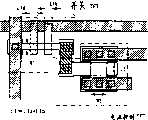
传统的有源矩阵型EL显示器的象素具有如图3所示的结构。在图3中,标号301表示一个用作开关元件(以下称作开关TFT)的TFT,302表示一个用作控制供应给EL元件303的电流的元件(电流控制元件)的TFT(以下称作电流控制TFT),304表示一个电容器(储存容量)。开关TFT 301与栅极线305和源极线306(数据线)相连。电流控制TFT 302的漏极与EL元件相连,源极与电流馈电线307相连。A pixel of a conventional active matrix type EL display has a structure as shown in FIG. 3 . In FIG. 3,
当选择栅极线305时,栅极开关TFT 301打开,然后源极线306的数据信号被储存到电容器304,并且电流控制TFT 302的栅极被打开。开关TFT 301的栅极关闭后,电流控制TFT 302的栅极由储存在电容器304中的电荷保持打开。在此间隔中EL元件303发光。EL元件303的发光量根据电流量改变。When the
此时,供应给EL元件303的电量受电流控制TFT 302的栅极电压控制。如图4所示。At this time, the amount of power supplied to the
图4(A)是电流控制TFT的晶体管特性曲线。标号401被称作Id-Vg特性(或Id-Vg曲线)。此处,Id是漏电流,Vg是栅压。从此曲线中可以得到对应于任意栅压的电流。FIG. 4(A) is a transistor characteristic curve of a current control TFT.
当EL元件被驱动时利用Id-Vg特性曲线的虚线402所示的区域。虚线402的闭合区域的放大图示于图4(B)。The region shown by the
在图4(B)中,斜线所示的区域被称作亚阈值区域。实际上,它表示一个栅压接近或小于阈值电压(Vth)的区域。漏极电流根据此区域中栅压的变化呈指数规律的变化。利用这种区域通过栅压控制电流。In FIG. 4(B), the region indicated by oblique lines is called a subthreshold region. In practice, it represents a region where the gate voltage is close to or less than the threshold voltage (Vth). The drain current varies exponentially with the gate voltage in this region. Use this area to control the current through the gate voltage.
通过打开开关TFT 301输入象素的数据信号首先被储存到电容器304,数据信号直接作用电流控制TFT 302的栅极电压。此时,关于栅压的漏电流根据图4(A)中的Id-Vg特性曲线一对一地确定。即给定电流流经对应于数据信号的EL元件303,EL元件303发射发光量对应于电流量的光。The data signal input to the pixel by turning on the
EL元件的发光量受数据信号的控制,如上所述,并因而进行灰度显示。这就称为模拟灰度法,在该方法中,通过改变信号的幅度来进行灰度显示。The amount of light emitted by the EL element is controlled by the data signal, as described above, and thus gray scale display is performed. This is called the analog grayscale method, in which grayscale display is performed by changing the amplitude of the signal.
但是也有一个缺点,即模拟灰度显示法在TFT的特性可变性上表现得非常力不从心。例如,假设开关TFT的Id-Vg特性不同于显示相同灰度的邻近象素的开关TFT的Id-Vg特性(即向着正或负侧漂移)。But there is also a disadvantage, that is, the analog grayscale display method is very weak in the characteristic variability of TFT. For example, assume that the Id-Vg characteristic of a switching TFT is different from that of a switching TFT of an adjacent pixel displaying the same gradation (ie, shifts toward the positive or negative side).
在此情形中,虽然依据于可变性的水平,但开关TFT的漏电流彼此不同,并因而可以把不同的栅压施加给每个象素的电流控制TFT。换言之,不同的电流流经每个EL元件,并因而发射不同的光量,并且不能实现相同灰度水平的显示。In this case, although depending on the level of variability, the leakage currents of the switching TFTs are different from each other, and thus different gate voltages can be applied to the current control TFTs of each pixel. In other words, different currents flow through each EL element, and thus emit different amounts of light, and display of the same gray level cannot be achieved.
另外,即使把相同的栅压提供给每个象素的电流控制TFT,如果电流控制TFT的Id-Vg特性有可变性,则不能输出相同的漏电流。另外,从图4(A)中清楚地看到,利用一个漏电流根据栅压的变化呈指数变化的区域,并且因此将发生一种情况:如果Id-Vg特性最轻微地移动,输出的电流量将变得非常不同,即使施加相同的栅压。如果这样,相邻象素在EL元件的发光量上将有很大的不同。In addition, even if the same gate voltage is supplied to the current control TFT of each pixel, if the Id-Vg characteristic of the current control TFT has variability, the same leakage current cannot be output. In addition, it is clear from FIG. 4(A) that a region in which the leakage current changes exponentially according to a change in the gate voltage is utilized, and thus a situation will occur that if the Id-Vg characteristic shifts the slightest, the output current The flow rate will become very different even with the same gate pressure applied. If so, adjacent pixels will have a large difference in the amount of light emitted from the EL element.
实际上,开关TFT和电流控制TFT的每个可变性协同工作,并且将被施以严格的条件。正如上述所述,模拟灰度法对TFT的特性可变性非常敏感,并已导致对实现传统有源矩阵型EL显示器件的多色显示有障碍。In fact, each variability of the switching TFT and the current controlling TFT works in tandem and will be subject to stringent conditions. As described above, the analog grayscale method is very sensitive to the variability of the characteristics of TFTs, and has resulted in obstacles to the realization of multicolor displays in conventional active matrix type EL display devices.
发明内容Contents of the invention
考虑了上述问题之后产生了本发明,因而本发明的目的在于提供一种能够进行清晰的多灰度彩色显示的有源矩阵型EL显示器件。本发明的另一个目的在于提供一种配置有这种有源矩阵型EL显示器件的高性能的电子设备。The present invention has been made in consideration of the above-mentioned problems, and an object of the present invention is to provide an active matrix type EL display device capable of clear multi-gradation color display. Another object of the present invention is to provide a high-performance electronic equipment equipped with such an active matrix type EL display device.
本申请人认为,要设计一种不影响TFT可变性的象素结构,数字灰度法好于传统的模拟灰度法,数字灰度法中电流控制TFT只用作供应电流的开关元件,模拟灰度法中EL元件的发光量通过控制电流而控制。The applicant believes that to design a pixel structure that does not affect the variability of the TFT, the digital grayscale method is better than the traditional analog grayscale method. In the digital grayscale method, the current control TFT is only used as a switching element for supplying current. In the grayscale method, the amount of light emitted by the EL element is controlled by controlling the current.
由此,本申请人认为在有源矩阵型EL显示器件中最理想的灰度显示是一种分级灰度显示法,具体地说,是一种基于时分法的灰度显示法(以下称为时分灰度或时分灰度显示)。Therefore, the applicant believes that the most ideal grayscale display in active matrix EL display devices is a graduated grayscale display method, specifically, a grayscale display method based on the time division method (hereinafter referred to as time-division grayscale or time-division grayscale display).
实际上,时分灰度显示按如下执行。此处给出的描述是关于根据8位数字驱动法进行256级灰度的全色显示的情形。Actually, time-division grayscale display is performed as follows. The description given here is about the case of performing full-color display of 256 gray levels according to the 8-bit digital driving method.
首先,一帧图形被分成八个子帧。此处,数据输入一个显示区域的所有象素时的一个周期称为一帧。标准EL显示器件中的振荡频率是60Hz,换言之,每秒钟形成60帧。当每秒的帧数小于此数时视觉开始感觉到图象闪烁。通过把一帧分割成多个帧而得到的分割的帧称作子帧。First, one frame of graphics is divided into eight subframes. Here, one cycle when data is input to all pixels of one display area is called one frame. The oscillation frequency in a standard EL display device is 60 Hz, in other words, 60 frames are formed per second. When the number of frames per second is less than this number, the visual perception begins to flicker. A divided frame obtained by dividing one frame into a plurality of frames is called a subframe.
一个子帧被分成一个寻址周期(Ta)和一个持续周期(Ts)。寻址周期是在一个子帧内把数据输入所有象素所需的全部时间,持续周期(或发光周期)是EL元件发光的周期(图10)。One subframe is divided into an address period (Ta) and a sustain period (Ts). The address period is the total time required to input data to all pixels within one subframe, and the sustain period (or light emission period) is the period in which the EL element emits light (FIG. 10).
此处,第一子帧称作SF1,从第二到第八子帧的其余子帧分别叫做SF2-SF8。寻址周期(Ta)在SF1-SF8中是常数。另一方面,对应于SF1-SF8的持续周期(Ts)分别称作TS1-Ts8。Here, the first subframe is called SF1, and the remaining subframes from the second to eighth subframes are called SF2-SF8, respectively. The address period (Ta) is constant in SF1-SF8. On the other hand, the sustain periods (Ts) corresponding to SF1-SF8 are referred to as TS1-Ts8, respectively.
此时,持续周期被分布成TS1∶Ts2∶Ts3∶Ts4∶Ts5∶Ts6∶Ts7∶Ts8=1∶1/2∶1/4∶1/8∶1/16∶1/32∶1/64∶1/128。但SF1-SF8出现的顺序并不重要。可通过合并持续周期而执行在256个灰度级中的理想灰度显示。At this time, the duration period is distributed as TS1: Ts2: Ts3: Ts4: Ts5: Ts6: Ts7: Ts8 = 1: 1/2: 1/4: 1/8: 1/16: 1/32: 1/64: 1/128. But the order in which SF1-SF8 appear is not important. Ideal gradation display among 256 gradation levels can be performed by combining the continuous periods.
首先,在电压不施与(或不被选取)一个象素的EL元件的反电极的状态下(应注意:反电极是不与TFT连接的电极;通常是阳极),数据信号被输入到每个象素,EL元件不发光。此周期被确定为寻址周期。当数据被输入到所有的象素并且寻址周期结束时,电压被施加到反电极,使得EL元件发光。此周期被确定为持续周期。发光期间(即象素发亮)的周期是TS1-Ts8中的任意一个。假设在Ts8周期内预定的象素发亮。First, in a state where a voltage is not applied (or not selected) to the counter electrode of the EL element of one pixel (it should be noted that the counter electrode is an electrode not connected to the TFT; usually an anode), a data signal is input to each pixel, the EL element does not emit light. This period is determined as an address period. When data is input to all pixels and the address period ends, a voltage is applied to the counter electrode, causing the EL element to emit light. This period is identified as the duration period. The cycle of the light-emitting period (that is, the lighting of the pixel) is any one of TS1-Ts8. Assume that predetermined pixels light up during the Ts8 period.
之后,再考虑寻址周期,数据信号被输入到所有象素并再进入持续周期。此时,持续周期是Ts1-Ts7中的任意一个。假设在Ts7周期内预定的象素发光。After that, considering the address period again, the data signal is input to all the pixels and enters the sustain period again. At this time, the sustain period is any one of Ts1-Ts7. Assume that predetermined pixels emit light during the Ts7 period.
之后,对剩余的六个子帧重复相同的操作,并通过以Ts6,Ts5,…Ts1的顺序设置连续的持续周期使预定象素在每个子帧内发亮。Thereafter, the same operation is repeated for the remaining six subframes, and predetermined pixels are made to light up in each subframe by setting continuous continuous periods in the order of Ts6, Ts5, . . . Ts1.
当出现八个子帧时即结束一帧。此时,象素的灰度通过增加持续周期控制。例如,当选择Ts1和Ts2时,假定总的光量是100%,则表现的亮度是75%,并当选择Ts3,Ts5和Ts8时,表现的亮度是16%。A frame ends when eight subframes occur. At this time, the gray level of the pixel is controlled by increasing the sustain period. For example, when Ts1 and Ts2 are selected, assuming that the total light quantity is 100%, the expressed brightness is 75%, and when Ts3, Ts5 and Ts8 are selected, the expressed brightness is 16%.
以上描述了256级的灰度显示,但可以执行其他的灰度显示。The 256-level gradation display has been described above, but other gradation display can be performed.
当执行n(n是大于或等于2的整数)位的灰度显示(2n灰度显示)时,一帧首先被分成n个子帧(SF1,SF2,SF3,…SF(n-1),和SF(n)),同时与n位灰度对应。一帧的分割数随着灰度级的增大而增加,并且驱动电路必须在高频下工作。When performing grayscale display of n (n is an integer greater than or equal to 2) bits (2n grayscale display), one frame is first divided into n subframes (SF1, SF2, SF3, ... SF(n-1), and SF(n)), corresponding to n-bit grayscale. The number of divisions of a frame increases as the gray level increases, and the driving circuit must work at high frequency.
n个子帧每个被分成寻址周期(Ta)和持续周期(Ts)。换言之,通过选择是否把电压施加到对于所有EL元件的反电极来选择地址和持续周期。Each of n subframes is divided into an address period (Ta) and a sustain period (Ts). In other words, the address and sustain period are selected by selecting whether to apply voltage to the counter electrodes for all EL elements.
并且,对应于n个子帧的每一个的持续周期被处理成TS1∶Ts2∶Ts3…Ts(n-1)∶Ts(n)=20∶2-1∶2-2∶…2-(n-2)∶2-(n-1)(此处,对应于的持续周期分别是TS1,Ts2,Ts3,…Ts(n-1)∶Ts(n))。And, the duration period corresponding to each of n subframes is processed as TS1:Ts2:Ts3...Ts(n-1):Ts(n)=20 :2-1 :2-2 :...2-(n -2) : 2-(n-1) (here, the corresponding duration periods are TS1, Ts2, Ts3, . . . Ts(n-1):Ts(n)).
在这种状态下,在一个随机帧中连续地选择一个象素(严格地说是选择每个象素的开关TFT),并且给电流控制TFT的栅电极施加一个预定的栅压。此时,被输入激励电流控制TFT的数据信号的象素的EL元件只在寻址周期结束后的分配给子帧的持续周期内发光。即预定的象素发光。In this state, one pixel is successively selected in a random frame (strictly speaking, the switching TFT of each pixel is selected), and a predetermined gate voltage is applied to the gate electrode of the current control TFT. At this time, the EL element of the pixel to which the data signal for driving the current control TFT is input emits light only in the continuous period allocated to the sub-frame after the address period ends. That is, predetermined pixels emit light.
在所有n个子帧内重复此操作,并通过增大持续周期控制每个象素的灰度。因此,当关注任意一个象素时,根据每个子帧内象素发亮的时间长短(即持续周期的持续长短)控制象素的灰度。This operation is repeated for all n subframes, and the gray level of each pixel is controlled by increasing the duration period. Therefore, when paying attention to any pixel, the gray level of the pixel is controlled according to the length of time the pixel is illuminated in each subframe (that is, the duration of the duration period).
如上所述,本发明最引人注目的特点在于分时灰度显示用于有源矩阵型EL显示器件。为了执行这种时分灰度,必须把一帧分成多个子帧。换言之,这比以前更需要提高驱动电路在数据信号侧和在栅极信号侧的工作频率。As described above, the most noticeable feature of the present invention is that time-division gray scale display is applied to an active matrix type EL display device. In order to perform such time-division gradation, one frame must be divided into a plurality of subframes. In other words, it is more necessary than before to increase the operating frequency of the drive circuit on the data signal side and on the gate signal side.
但是,要使TFT能在常规的多晶硅膜(多晶硅)上以这样高的速度工作是很困难的。工作频率可通过把数据信号侧的驱动电路分成多个电路而降低,但如果这样,就不能实现令人满意的结果。However, it is difficult to make a TFT operate at such a high speed on a conventional polysilicon film (polysilicon). The operating frequency can be lowered by dividing the driving circuit on the data signal side into a plurality of circuits, but in this case, satisfactory results cannot be achieved.
因此,在本发明中利用一种具有特定的晶体结构的硅膜,晶界的连续性高,晶体单向取向。该膜用作TFT的一个有源层,因而使得TFT显示出极高的操作性和速度。即这也是本发明的一个特点,通过利用这种高工作速度的TFT进行有源矩阵型EL显示器件的时分灰度显示。下面对实验所做的用于本发明中的硅膜的观察结果进行描述。Therefore, in the present invention, a silicon film having a specific crystal structure is used, the continuity of the grain boundaries is high, and the crystals are unidirectionally oriented. This film serves as an active layer of the TFT, thus enabling the TFT to exhibit extremely high operability and speed. That is to say, this is also a characteristic of the present invention, and the time-division grayscale display of the active matrix EL display device is performed by using such a high-speed TFT. The following describes experimentally observed results of the silicon film used in the present invention.
用在本发明中的硅膜有一种晶体结构,该结构中微观的众多针状晶体或棒状晶体(以下称作棒晶)聚集在一起并形成线条。这从TEM(透射电子显微镜)的观察中可以很容易地被确认。The silicon film used in the present invention has a crystal structure in which microscopically numerous needle-like crystals or rod-like crystals (hereinafter referred to as rod crystals) gather together and form lines. This can be easily confirmed from TEM (Transmission Electron Microscope) observation.
另外,作为涉及到用于本发明中硅膜的光斑直径大约1.35μm的电子束衍射图象的详细观察结果,对应于{110}平面的衍射光斑尽管有轻微地波动,但仍规律地出现,并且虽然晶轴有轻微的偏移,但可以确认定以{110}面为主取向面。In addition, as a result of detailed observation of electron beam diffraction images related to the silicon film used in the present invention with a spot diameter of about 1.35 µm, the diffraction spots corresponding to the {110} plane regularly appeared although slightly fluctuating, And although the crystal axis is slightly shifted, it can be confirmed that the {110} plane is the main orientation plane.
图19(A)表示一个通过向用于本发明中的硅膜上透射光斑直径大约为1.35μm的电子束而获得的电子束衍射图象。另一方面,图19(B)表示通过在相同的条件下把电子束投影到传统的多晶硅膜上而获得的电子束衍射图象。在每个图中,图片的中心是电子束投影的一个位置(电子束的投影点)。Fig. 19(A) shows an electron beam diffraction image obtained by transmitting an electron beam having a spot diameter of about 1.35 µm onto a silicon film used in the present invention. On the other hand, Fig. 19(B) shows an electron beam diffraction image obtained by projecting an electron beam onto a conventional polysilicon film under the same conditions. In each figure, the center of the picture is a position where the electron beam is projected (projection point of the electron beam).
对应于{110}平面的衍射光斑在图19(A)中表现得比较规则,而在图19(B)中分布得十分不规则,并因而取向面明显地不均匀。从这幅电子束衍射图片中可以看出,用于本发明中的硅膜与传统的多晶硅膜可以即刻区分开来。The diffraction spots corresponding to the {110} plane appear relatively regular in FIG. 19(A), but are quite irregularly distributed in FIG. 19(B), and thus the orientation plane is obviously uneven. As can be seen from this electron beam diffraction picture, the silicon film used in the present invention can be instantly distinguished from the conventional polysilicon film.
在图19(A)的电子束衍射图象中,通过与{110}取向的单晶硅片的电子束衍射图象相比,明显地显示出对应于{110}平面的衍射斑。另外,虽然单晶硅片的衍射斑看做一个细点,但用于本发明中的硅膜的衍射斑有一个以电子束的投影点为中心的同心圆环的扩展。In the electron beam diffraction image of FIG. 19(A), diffraction spots corresponding to {110} planes are clearly shown by comparison with the electron beam diffraction image of a {110}-oriented silicon single crystal wafer. In addition, although the diffraction spot of the single crystal silicon wafer is regarded as a fine point, the diffraction spot of the silicon film used in the present invention has a concentric circular ring expansion centered on the projected point of the electron beam.
这也是用于本发明中的硅膜的一个特点。因为{110}平面对每个晶粒都有一个单独的取向面,所以只要涉及一个晶粒,就可以有望获得如同单晶硅的衍射斑。但实际上,存在着多个晶粒的集合,并因而每个晶粒都有一个围绕晶轴的轻微旋转,虽然每个晶粒确定一个以{110}平面作为其取向面,对应于晶粒的多个衍射光点呈现在该同心圆环。光点彼此有叠合,以致表现出一种扩展。This is also a feature of the silicon film used in the present invention. Because the {110} plane has a separate orientation plane for each grain, as long as a single grain is involved, it can be expected to obtain a diffraction spot like a single crystal silicon. But in fact, there is a collection of multiple grains, and thus each grain has a slight rotation around the crystal axis, although each grain defines a {110} plane as its orientation plane, corresponding to the grain Multiple diffracted spots appear in the concentric rings. The points of light overlap each other so that they appear to expand.
但因为每个单独的晶粒形成一个连续性极好的晶界,如后续所述,所以绕晶轴的轻微旋转不构成毁坏结晶度的因素。因此,可以说用于本发明中的硅膜的电子束衍射图象与{110}取向的单晶硅片的电子束衍射图象没有区别。But because each individual crystal grain forms a grain boundary with excellent continuity, as described later, slight rotation around the crystal axis does not constitute a factor that destroys crystallinity. Therefore, it can be said that the electron beam diffraction pattern of the silicon film used in the present invention is not different from that of the {110}-oriented single crystal silicon wafer.
从前述内容可以肯定,在本发明中用作TFT有源层的硅膜是表现出对应于{110}取向的电子束衍射图象的硅膜。As can be ascertained from the foregoing, the silicon film used as the active layer of the TFT in the present invention is a silicon film exhibiting an electron beam diffraction image corresponding to the {110} orientation.
下面,将对用在本发明中的硅膜的晶界给予描述。虽然为了方便起见描述是针对“晶界”这一名称,但可以认为是一个晶粒与另一个从那儿衍生(或分支出的)晶粒之间的界面。无论如何,在本说明书中采用包括上述界面含义的“晶界”名称。Next, a description will be given of the grain boundaries of the silicon film used in the present invention. Although the description is for the name "grain boundary" for convenience, it can be considered as an interface between one grain and another grain derived (or branched) therefrom. In any case, the name "grain boundary" including the meaning of the above-mentioned interface is used in this specification.
本申请人从对晶界的观察中确认,在晶界的晶格中具有连续性,其中晶界由在HR-TEM(高分辨率透射电子显微镜)下的单个棒状晶体的接触构成。这可以从观察到的在晶界中晶格条纹彼此连续地连接这一事实中很容易地得到肯定。The present applicant confirmed that there is continuity in the crystal lattice of the grain boundary from the observation of the grain boundary consisting of contacts of individual rod-like crystals under HR-TEM (High Resolution Transmission Electron Microscopy). This can be easily confirmed from the observed fact that the lattice fringes are continuously connected to each other in the grain boundaries.
晶界中晶格的连续性产生于晶界是一个称作“平面边界”这一事实。在说明书中平面边界的定义是从“Planar Boundary”一词演变而来,该词出现在“Characterization of High-Efficiency Cast-Si Solar Cell Wafersby MBIC Measurement;Ryuichi Shimokawa and Yutaka Hayashi,JapaneseJournal of Applied Physics vol.27,No.5,pp.751-758,1988”。The continuity of the lattice in the grain boundaries arises from the fact that the grain boundaries are a so-called "planar boundary". The definition of planar boundary in the manual is derived from the term "Planar Boundary", which appeared in "Characterization of High-Efficiency Cast-Si Solar Cell Wafers by MBIC Measurement; Ryuichi Shimokawa and Yutaka Hayashi, Japanese Journal of Applied Physics vol. 27, No.5, pp.751-758, 1988".
根据上述内容,平面边界包括一个孪晶界,一个特定的层错和一个特定的扭曲晶界。此平面边界具有电惰性的特点。即虽然它是一个因平面边界不用作陷阱去阻止载流子运动的晶界,但事实上可以认为它不存在。According to the above, the planar boundary includes a twin boundary, a specific stacking fault and a specific twisted grain boundary. This planar boundary is characterized by electrical inertia. That is, although it is a grain boundary because the planar boundary does not serve as a trap to prevent the movement of carriers, it can be considered as non-existent in fact.
尤其是,当晶轴(垂直于晶面的轴)是<110>轴时,{211}孪晶界和{111}孪晶界通常被称作∑3的相应晶界。∑值是一个用作表示相应晶界连续性水平的指示器的参数,并且已知晶界连续性随着∑值的下降而变优。In particular, when the crystallographic axis (axis perpendicular to the crystal plane) is the <110> axis, {211} twin boundaries and {111} twin boundaries are often referred to as corresponding grain boundaries of Σ3. The Σ value is a parameter used as an indicator representing the level of the corresponding grain boundary continuity, and it is known that the grain boundary continuity becomes better as the Σ value decreases.
通过TEM观察本发明中所使用的硅膜的结果是几乎所有的晶界都被证明为是∑3的相应晶界。这从θ=70.5°时两晶粒之间形成的晶界变为∑3的相应晶界这一事实中得以判定,其中θ是当两晶粒的平面取向为{110}时对应于{111}平面的晶格条纹间形成的角度。As a result of observing the silicon film used in the present invention by TEM, almost all grain boundaries were confirmed to be the corresponding grain boundaries of Σ3. This is judged from the fact that the grain boundary formed between the two grains becomes the corresponding grain boundary of Σ3 when θ = 70.5°, where θ is corresponding to {111 when the plane orientation of the two grains is {110} } The angle formed between the lattice fringes of the plane.
注意到,当θ=38.9°时晶界变成∑9的相应晶界。并且还存在其他的晶界,如这种晶界。Note that the grain boundary becomes the corresponding grain boundary of Σ9 when θ = 38.9°. And there are other grain boundaries like this grain boundary.
晶体结构(更精确地说,晶界的结构)表示两个晶界不同的晶粒彼此以非常好的连续性连接。换言之,建立了一种晶格在晶界内连续延伸的结构,并且要从晶体的缺陷中产生一个陷阱能级非常困难。因此,具有上述结构的半导体薄膜事实上认为没有晶界。The crystal structure (more precisely, the structure of the grain boundaries) means that two crystal grains with different grain boundaries are connected to each other in very good continuity. In other words, a structure is established in which the lattice extends continuously within the grain boundaries, and it is very difficult to generate a trap level from a defect in the crystal. Therefore, the semiconductor thin film having the above structure is considered to have virtually no grain boundaries.
通过TEM观察确定,当形成用于本发明中的硅膜时存在于晶粒中的缺陷(堆积缺陷等)通过以连续的步骤在700-1150℃下的加热处理而几乎完全消失。这从加热前后缺陷的数量大大减少这一事实中显得很明显。It was confirmed by TEM observation that defects (stacking defects, etc.) present in crystal grains when forming the silicon film used in the present invention almost completely disappeared by heat treatment at 700-1150° C. in successive steps. This is evident from the fact that the number of defects is greatly reduced before and after heating.
根据电子自旋共振分析(ESR分析),缺陷数量的差别表现为自旋强度的差别。在当前状态下,用于本发明中的硅膜的自旋强度被证明至多为5×10¹⁷转/cm3(最好至少3×1017转/cm3)。但是,因为此测量值接近测量器件的检测极限,所以希望实际的自旋强度更小。According to electron spin resonance analysis (ESR analysis), the difference in the number of defects appears as a difference in spin intensity. In the current state, the spin intensity of the silicon film used in the present invention has been demonstrated to be at most 5×10¹⁷ turns/cm3 (preferably at least 3×10¹⁷ turns/cm3 ). However, since this measured value is close to the detection limit of the measurement device, the actual spin intensity is expected to be smaller.
本申请人1998年提出的044659号申请、1998年提出的152316号申请、1998年提出的152308号申请以及1998年提出的152305号申请分别给出了关于用于本发明中的硅膜更详细的描述。No. 044659 application filed by the applicant in 1998, No. 152316 application filed in 1998, No. 152308 application filed in 1998, and No. 152305 application filed in 1998 provided more detailed information about the silicon film used in the present invention respectively. describe.
其中用于本发明的硅膜实验上由一个有源层制成的TFT表现出等同于MOSFET的电学特性。从本发明人实验上制成的TFT(其中的有源层厚度为30nm,栅极绝缘膜的厚度为100nm)上可获得如下数据。A TFT in which the silicon film used in the present invention was experimentally made of an active layer exhibited electrical characteristics equivalent to MOSFETs. The following data were obtained from a TFT (in which the thickness of the active layer was 30nm and the thickness of the gate insulating film was 100nm) fabricated experimentally by the present inventors.
(1)作为开关性能指标的亚阈值系数(on/off操作开关的快慢),N沟道型TFT和P沟道型TFT的是60~100mV/decade(典型值60~85mV/decade),该值很小。(1) The sub-threshold coefficient (speed of on/off operation switch) as a switch performance indicator is 60-100mV/decade (typical value 60-85mV/decade) for N-channel TFT and P-channel TFT. The value is small.
(2)作为TFT操作速度指标的电子场效应迁移率(μFE),N沟道型TFT的是200~650cm2/Vs(典型值是300~500cm2/Vs),P沟道型TFT的是100~300cm2/Vs(150-200cm2/Vs)。这些值很大。(2) Electron field-effect mobility (μFE ), which is an indicator of TFT operation speed, is 200 to 650 cm2 /Vs (typically 300 to 500 cm2 /Vs) for N-channel TFTs and 200 to 500 cm 2 /Vs for P-channel TFTs. It is 100-300 cm2 /Vs (150-200 cm2 /Vs). These values are large.
(3)作为TFT驱动电压指标的阈值电压(Vth),N沟道型TFT的是-0.5~1.5,P沟道型TFT的是-1.5~0.5。这些值小。(3) The threshold voltage (Vth ), which is an index of the TFT driving voltage, is -0.5 to 1.5 for an N-channel TFT and -1.5 to 0.5 for a P-channel TFT. These values are small.
上述器件已被证实能够实现优越的开关性能和高速的操作性能。另外,在利用TFT制造的环形振荡器中,最大可以得到大约1GHz的振荡频率。环形振荡器的构造如下。The above devices have been proven to achieve superior switching performance and high-speed operation. In addition, in a ring oscillator manufactured using TFTs, an oscillation frequency of about 1 GHz can be obtained at the maximum. The ring oscillator is constructed as follows.
级数:九级:Number of levels: Nine levels:
TFT栅极绝缘膜的膜厚度:30nm和50nm;Film thickness of TFT gate insulating film: 30nm and 50nm;
TFT的栅级宽度(沟道长度):0.6μmTFT gate width (channel length): 0.6μm
另外,作为实际制作移位寄存器并确定操作频率的结果,在移位寄存器中得到100MHz操作频率的输出脉冲,其中栅极绝缘膜的厚度是30nm,栅级宽度是0.6μm,电源电压是5V,步骤数为50。In addition, as a result of actually fabricating the shift register and determining the operating frequency, an output pulse at an operating frequency of 100 MHz was obtained in the shift register, where the thickness of the gate insulating film was 30 nm, the gate width was 0.6 μm, and the power supply voltage was 5 V. The number of steps is 50.
上述环形振荡器和移位寄存器的好的数据表示,用在本发明中的硅膜由有源层制成的TFT等价于使用单晶硅的MOSFET,或具有超过MOSFET的操作性能。The good data of the above-mentioned ring oscillator and shift register indicate that the silicon film used in the present invention is used in a TFT made of an active layer which is equivalent to a MOSFET using single crystal silicon, or has an operation performance exceeding that of a MOSFET.
附图说明Description of drawings
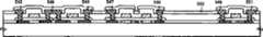
图1A和1B表示EL显示器件的结构。1A and 1B show the structure of an EL display device.
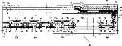
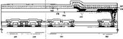
图2表示EL显示器件的截面结构。Fig. 2 shows a cross-sectional structure of an EL display device.
图3表示传统EL显示器件的象素部分的结构。Fig. 3 shows the structure of a pixel portion of a conventional EL display device.
图4A和4B是解释模拟灰度法中使用的TFT的特性示图。4A and 4B are diagrams explaining characteristics of TFTs used in the analog grayscale method.
图5A-5E表示EL显示器件的制作步骤。5A to 5E show the manufacturing steps of the EL display device.
图6A-6D表示EL显示器件的制作步骤。6A-6D show the manufacturing steps of the EL display device.
图7A-7D表示EL显示器件的制作步骤。7A-7D show the manufacturing steps of the EL display device.
图8A-8C表示EL显示器件的制作步骤。8A-8C show the manufacturing steps of the EL display device.
图9是EL显示器件象素部分的放大示图。Fig. 9 is an enlarged view of a pixel portion of an EL display device.
图10是解释时分灰度法的操作模式的示图。FIG. 10 is a diagram for explaining an operation mode of the time-division grayscale method.
图11表示EL模块的外部形状。Fig. 11 shows the external shape of the EL module.
图12A和12B表示EL模块的外部形状。12A and 12B show the external shape of the EL module.
图13A-13C表示连接结构的制作步骤。13A-13C show the fabrication steps of the connection structure.
图14表示EL显示器件象素部分的结构。Fig. 14 shows the structure of a pixel portion of an EL display device.
图15表示EL显示器件的截面结构。Fig. 15 shows a cross-sectional structure of an EL display device.
图16表示EL显示器件象素部分的上表面结构。Fig. 16 shows the upper surface structure of the pixel portion of the EL display device.
图17表示EL显示器件象素部分的上表面结构。Fig. 17 shows the upper surface structure of the pixel portion of the EL display device.
图18A-18E表示电子设备的一个具体实例。18A-18E show a specific example of electronic equipment.
图19A和图19B是代替插图的照片,表示多晶硅膜的电子束衍射图象。19A and 19B are photographs instead of illustrations showing electron beam diffraction images of polysilicon films.
图20A和20B是代替插图的照片,表示本发明EL显示器件的显示图象的实例。20A and 20B are photographs instead of illustrations showing examples of display images of the EL display device of the present invention.
具体实施方式Detailed ways
首先,本发明有源矩阵型EL显示器件的电路结构示于图1(A)中。在图1(A)所示的有源矩阵型EL显示器件中,象素部分101,数据信号侧驱动电路102,和设置在象素部分周围的栅极信号侧驱动电路103通过形成在基底上的TFT形成。或者,数据侧信号驱动电路和栅极侧信号驱动电路可以以一对电路的形式将象素部分夹在其间设置。First, the circuit structure of the active matrix type EL display device of the present invention is shown in FIG. 1(A). In the active matrix type EL display device shown in FIG. 1(A), the pixel portion 101, the data signal side driver circuit 102, and the gate signal side driver circuit 103 arranged around the pixel portion are formed on the substrate by TFT formation. Alternatively, the data side signal driver circuit and the gate side signal driver circuit may be provided as a pair of circuits sandwiching the pixel portion therebetween.
数据信号侧驱动电路102基本包括一个移位寄存器102a,一个锁存器(A)102b,和一个锁存器(B)102c。时钟脉冲(CK)和起始脉冲(SP)输入到移位寄存器102a,数字数据信号输入到锁存器(A)102b,锁存信号输入给锁存器(B)102c。The data signal side driver circuit 102 basically includes a shift register 102a, a latch (A) 102b, and a latch (B) 102c. A clock pulse (CK) and a start pulse (SP) are input to the shift register 102a, a digital data signal is input to the latch (A) 102b, and a latch signal is input to the latch (B) 102c.
在本发明中,输入给象素部分101的数据信号是一个数字信号,并且虽然是在液晶显示器件中实施,但并不执行电压灰度显示。因此,具有信息“0”或“1”的数字数据信号直接输入给象素部分101。In the present invention, the data signal input to the pixel portion 101 is a digital signal, and although implemented in a liquid crystal display device, voltage grayscale display is not performed. Therefore, a digital data signal having information "0" or "1" is directly input to the pixel portion 101.
多个象素104布置成类似矩阵的象素部分101。象素104的放大图示于图1(B)。在图1(B)中,标号105表示一个开关TFT。此开关与用于输入栅极信号的栅极线106相连,并还与输入数据信号的数据线107(也称作源极线)相连。A plurality of pixels 104 are arranged in the pixel portion 101 like a matrix. An enlarged view of the pixel 104 is shown in FIG. 1(B). In FIG. 1(B), reference numeral 105 denotes a switching TFT. This switch is connected to a
标号108表示电流控制TFT。栅极与开关TFT105的漏极相连。电流控制TFT 108的漏极与EL元件109相连,其源极与馈电线110相连。EL元件109由一个与电流控制TFT 108相连的阳极(象素电极)和一个面对该阳极的阴极(反电极)组成,EL层位于阳极和阴极之间。阴极与给出的电源线111相连。Reference numeral 108 denotes a current control TFT. The gate is connected to the drain of the switching TFT105. The drain of the current control TFT 108 is connected to the EL element 109, and the source thereof is connected to the
当开关TFT 105处于非选定态(断开状态)时,设置一个电容器112以维持电流控制TFT 108的栅压。电容器112与开关105的漏极以及馈电线110相连。A
输入给上述象素部分的数字数据信号由时分灰度数据信号发生电路113产生。电路113把包括模拟信号或数字信号的视频信号(包含图象信息)转变成数字数据信号,以进行时分灰度显示并产生为进行时分灰度显示所需的时间脉冲等。The digital data signal input to the above-mentioned pixel portion is generated by the time-division gradation data signal generation circuit 113 . The circuit 113 converts video signals (including image information) including analog signals or digital signals into digital data signals for time-division grayscale display and generates time pulses etc. required for time-division grayscale display.
典型地,时分灰度数据信号发生电路113包括一个把一帧分成n个对应于n位灰度的子帧的器件(n是不小于2的整数),一个用于在n个子帧中选择寻址周期和持续周期的器件,和一个把持续周期设置成Ts1∶Ts2∶Ts3∶……Ts(n-1)∶Ts(n)=20∶2-1∶2-2∶……2-(n-2)∶2-(n-1)的器件。Typically, the time-division grayscale data signal generating circuit 113 includes a device for dividing a frame into n subframes corresponding to n-bit grayscales (n is an integer not less than 2), and a device for selecting the subframes among the n subframes. address period and sustain period, and a device that sets the sustain period as Ts1: Ts2: Ts3: ... Ts(n-1): Ts(n) = 20 : 2-1 :2 -2 : ... 2- (n-2) : 2-(n-1) devices.
时分灰度数据信号发生电路113可以设置在本发明EL显示器件的外部。如果这样,产生在那个位置的数字数据信号被输入到本发明的EL显示器件。在这种情况下,具有本发明的EL显示器件作为显示板的电子设备将包括EL显示器件和作为不同组份的本发明的时分灰度数据信号发生电路。The time-division grayscale data signal generating circuit 113 can be arranged outside the EL display device of the present invention. If so, the digital data signal generated at that position is input to the EL display device of the present invention. In this case, electronic equipment having the EL display device of the present invention as a display panel will include the EL display device and the time-division gradation data signal generating circuit of the present invention as different components.
另外,时分灰度数据信号发生电路113可以以IC片的形式设置在本发明EL显示器件上。如果这样,产生于IC片的数字数据信号输入到本发明的EL显示器件。在这种情况下,具有本发明的EL显示器件作为显示板的电子设备将包括本发明的EL显示器件,在该显示器件上设置一个作为一个组成部分的包含时分灰度数据信号发生电路的IC片。In addition, the time-division grayscale data signal generating circuit 113 can be provided on the EL display device of the present invention in the form of an IC chip. If so, the digital data signal generated from the IC chip is input to the EL display device of the present invention. In this case, electronic equipment having the EL display device of the present invention as a display panel will include the EL display device of the present invention on which an IC including a time-division gradation data signal generating circuit is provided as a component piece.
最后,时分灰度数据信号发生电路113可以由设置在与象素部分104相同的TFT、数据信号侧驱动电路102和栅极信号侧驱动电路构成。如果这样,当包括图象信息的视频信号输入到EL显示器件中时所有的信号都可以处理。在这种情况下,最好通过TFT构建时分灰度数据信号发生电路,其中如上所述,用在本发明中的硅膜被制成一个有源层。另外,在这种情况下,具有本发明的EL显示器件作为显示板的电子设备这样构成:时分灰度数据信号发生电路构建在EL显示器件本身当中。因而,电子设备可以制得更密集。Finally, the time-division gradation data signal generation circuit 113 can be constituted by the TFT provided in the same pixel portion 104, the data signal side driver circuit 102, and the gate signal side driver circuit. If so, all signals can be processed when a video signal including image information is input to the EL display device. In this case, it is preferable to construct the time-division gradation data signal generating circuit by TFT in which the silicon film used in the present invention is formed as an active layer as described above. In addition, in this case, electronic equipment having the EL display device of the present invention as a display panel is constituted such that a time-division gradation data signal generating circuit is built in the EL display device itself. Thus, electronic equipment can be made denser.
接下来参见图2所示的本发明有源矩阵型EL显示器件的截面结构图。Next, refer to FIG. 2 which is a cross-sectional structure diagram of the active matrix EL display device of the present invention.
在图2中,标号11是一个基底,12是一个作为基础的绝缘膜(以下该膜称作基膜)。对于基底11,可以用透光型基底,典型的有玻璃基底、石英基底,玻璃陶瓷基底或晶体玻璃基底。但他们必须在制造过程中耐最高的处理温度。In FIG. 2,
基膜12对用于具有可移动离子或有导电性的基底尤其有效,但不需要设置在石英基底上。包含硅的绝缘膜可用作基膜12。应注意,在本说明书中“包含硅的绝缘膜”表示以预定的比例(SiOxNy∶x和y为任一整数)加入了氧或氮的绝缘膜,如氧化硅膜,氮化硅膜或氮化硅氧化膜。标号201是一个开关TFT,202是电路控制TFT。这两个TFT都由n沟道型TFT构成。因为n沟道型TFT的场效应电子迁移率大于p沟道型TFT的场效应电子迁移率,n沟道型TFT可以以较高的操作速度工作,并使得很大的电流很容易地通过。关于通过相同量的电流时所需的TFT的大小,n沟道型TFT的较小。因此,希望用n沟道型TFT作为电流控制TFT,因为图象显示板的有效发光面积加宽。The
但在本发明中,不需要将开关TFT和电流控制TFT限制为n沟道型TFT。对于上述两种TFT也可以用p沟道型TFT。However, in the present invention, it is not necessary to limit the switching TFT and the current control TFT to n-channel type TFTs. A p-channel type TFT can also be used for the above two TFTs.
开关TFT由一个有源层制成,包括一个源极区13,一个漏极区14,LDD区15a-15d,绝缘区16,沟道成形区17a,17b,栅极绝缘膜18,栅电极19a,19b,第一层间绝缘膜20,源极线21和漏极线22。栅极绝缘膜18或第一层间绝缘膜20对于基底上的所有TFT共用,或可以根据电路或元件而改变。The switching TFT is made of an active layer including a
在图2所示的开关TFT201中,栅电极19a,19b电连接,换言之,建立所谓的双栅极结构。当然,不仅可以建立双栅结构,还可以建立所谓的多栅结构,如三栅极结构。多栅结构表示一种包括有源层的结构,有两个沟道形成区或多个串联连接的沟道形成区。In the switching
多栅结构对减小OFF态电流非常有效,并且如果开关TFT的OFF态电流减的足够小,可以减小对图1(B)所示电容器112电容的需求。也就是因为电容器112的占有面积可以减小,所以多栅结构也可以有效地加宽EL元件109的有效发光面积。The multi-gate structure is very effective in reducing the OFF state current, and if the OFF state current of the switching TFT is reduced enough, it can reduce the demand for the capacitance of the
在开关TFT 201中,LDD区15a-15d设置成不与栅电极19a和19b叠合,栅极绝缘膜18夹在其间。由此建立的结构对于减小OFF态电流非常有效。LDD区的长度(宽度)为0.5-3.5μm,代表性的值为2.0-2.5μm。In the switching
要减小OFF态电流,在沟道成形区和LDD区之间形成一个偏移区(即由成份与沟道成形区相同的半导体层形成的区域,该区不施加栅压)更为理想。在有两个或多个栅电极的多栅结构中,形成在沟道成形区之间的绝缘区16(即浓度相同并加入相同掺杂元素作为源区或漏极区)对减小OFF态电流有效。To reduce the OFF state current, it is more ideal to form an offset region between the channel forming region and the LDD region (that is, a region formed of the same semiconductor layer as the channel forming region, and no gate voltage is applied to this region). In a multi-gate structure with two or more gate electrodes, the insulating
电流控制TFT 202由一个有源层制成,包括一个源区26,一个漏极区27,一个LDD区28,一个沟道形成区29,一个栅极绝缘膜18,一个栅电极30,第一层间绝缘膜20,一个源极线31和一个漏极线32。栅电极30可以以单栅极结构代替多栅极结构。The
开关TFT的漏极连接到电流控制TFT的栅极,如图1(B)所示。具体地说,控制电流TFT 202的栅电极30与开关TFT 201的漏极区14经漏极线22(也称作连接线)电连接。源极线31连接到图1(B)的馈电线110。The drain of the switching TFT is connected to the gate of the current controlling TFT, as shown in Fig. 1(B). Specifically, the
电流控制TFT 202是一个控制供应给EL元件的电流量的元件,从那儿可以流过较大量的电流。因此,沟道宽度(W)最好设计成大于开关TFT的沟道宽度。另外,沟道长度最好设计成过量的电流不能流过电流控制TFT 202。对每个象素的理想电流值是0.5-2μA(1-1.5μA最好)。The
据前面所述,W1最好为0.1-5μm(代表值为1-3μm),W2为0.5-30μm(代表值为2-10μm),L1为0.2-18μm(代表值为2-15μm),L2为0.1-50μm(代表值为1-20μm),这里L1是开关TFT的沟道长度(L1+L1a+L1b),W1是该沟道的宽度,L2是电流控制TFT的沟道长度,W2是该沟道的宽度,如图9所述。According to the above, W1 is preferably 0.1-5 μm (representative value is 1-3 μm), W2 is 0.5-30 μm (representative value is 2-10 μm), L1 is 0.2-18 μm (representative value is 2-15 μm), L2 0.1-50μm (representative value is 1-20μm), where L1 is the channel length of the switching TFT (L1+L1a+L1b), W1 is the width of the channel, L2 is the channel length of the current control TFT, and W2 is The width of the channel is as described in FIG. 9 .
图2所示的EL显示器件还有一个特点,即在电流控制TFT 202中,LDD形成在漏极区27和沟道成形区29之间,另外,LDD区28有一个与栅电极30重叠的区域和一个不与栅电极30重叠的区域,栅极绝缘膜18位于LDD区28和栅电极30之间。The EL display device shown in FIG. 2 also has a feature that in the
电流控制TFT 202能通过较大的电流量以致EL元件203发光,还希望设想出一个关于热载流子注入导致的劣化的对策。当显示黑色时电流控制TFT 202保持在截止状态。在这种情况下,如果截止态电流很高,则不能显示出诱人的黑色,并且产生对比度的下降。因此,还需要抑制截止态电流。The
关于热载流子注入导致的劣化,已知LDD与栅电极叠合的结构非常有效。但因为如果LDD区全部栅电极重合则截止态电流增大,所以本申请人通过提供一种新的结构而同时解决了对热载流子和截止态电流的对策的问题,新结构中除了前述结构外,不与栅电极重合的LDD区串联设置。With regard to degradation due to hot carrier injection, it is known that the structure in which the LDD and the gate electrode are stacked is very effective. However, because the off-state current increases if all the gate electrodes of the LDD region overlap, the applicant has solved the problem of countermeasures against hot carriers and off-state current by providing a new structure. In the new structure, in addition to the aforementioned Outside the structure, the LDD region not overlapping with the gate electrode is arranged in series.
此时,与栅电极叠合的LDD区的长度设计成0.1-3μm(最好是0.1-1.5μm)。如果长度过长,则寄生电容(不希望的电容)增大,而如果过短,则阻止热载流子的效果减弱。不与栅电极叠合的LDD区的长度设计成1.0-3.5μm(最好是1.5-2.0μm)。如果该长度过长,则不能流过充足的电流,而如果长度过短,则减小截止态电流的效果减弱。At this time, the length of the LDD region overlapping with the gate electrode is designed to be 0.1-3 μm (preferably 0.1-1.5 μm). If the length is too long, parasitic capacitance (undesired capacitance) increases, while if it is too short, the effect of blocking hot carriers is weakened. The length of the LDD region not overlapping the gate electrode is designed to be 1.0-3.5 µm (preferably 1.5-2.0 µm). If the length is too long, sufficient current cannot flow, and if the length is too short, the effect of reducing the off-state current is weakened.
因为在上述结构中寄生电容形成于栅电极和LDD区彼此叠合的区域中,所以希望在源极区26和沟道成形区29之间不出现寄生电容。所有需要的是只把LDD设置在漏极区一侧,因为控制电流TFT中的载流子(此处为电子)流动方向总是相同。Since the parasitic capacitance is formed in the region where the gate electrode and the LDD region overlap each other in the above structure, it is desirable that no parasitic capacitance occurs between the
从增加通过的电流量的角度看,增加电流控制TFT 202的有源层(尤其是沟道形成区)膜厚也有效(50-100nm较好,60-80nm更好)。另一方面,从减小开关TFT 201中截止态电流的角度看,减小有源层(尤其是沟道形成区)的膜厚也有效(20-50nm较好,25-40nm更好)。From the perspective of increasing the amount of passing current, it is also effective to increase the film thickness of the active layer (especially the channel forming region) of the current control TFT 202 (50-100nm is better, 60-80nm is better). On the other hand, from the viewpoint of reducing the off-state current in the switching
以上描述了形成在象素中的TFT结构。在此结构中还同时形成一个驱动电路。身为一个形成驱动电路的基本单元的CMOS电路适于图2。The TFT structure formed in the pixel is described above. A driving circuit is also formed in this structure at the same time. A CMOS circuit as a basic unit forming a driving circuit is suitable for FIG. 2 .
在图2中,把具有减小热载流子注入但不把操作速度减到最小的结构的TFT用作CMOS电路的n沟道型TFT 204。在此描述的驱动电路是数据信号侧驱动电路102和栅极信号侧驱动电路103,二者均示于图1。当然,也可以形成其他的逻辑电路(电平转换器,A/D转换器,信号分配电路等)。In FIG. 2, a TFT having a structure that reduces hot carrier injection but does not minimize the operation speed is used as an n-
n沟道型TFT 204的有源层包括一个源极区35,一个漏极区36,一个LDD区37,和一个沟道成形区38。LDD区37与栅电极39叠合,栅极绝缘膜18夹插其间。The active layer of the n-
只在漏极区一侧上形成LDD区的理由不是为了降低操作速度。不需要担心n沟道型TFT 204中的截止态电流值。相反,应在该电流值之上确定操作速度。因此,LDD区37最好完全位于栅电极上,由此尽可能地减小电阻成份。也即可以省去所谓的补偿。The reason for forming the LDD region only on the drain region side is not to reduce the operating speed. There is no need to worry about the off-state current value in the n-
在CMOS电路的p沟道型TFT205中,不需要特别地提供LDD区,因为热载流子注入导致的劣化可以忽略。因此,有源层包括一个源区40,一个漏极区41,一个沟道成形区42。栅极绝缘膜18和栅电极43设置在其上。当然还可以设置LDD区和n沟道型TFT 204,以对热载流子采取对策。In the p-
当p沟道型TFT用作电路控制TFT 202时,可以有与p沟道型TFT205有相同的结构。When a p-channel type TFT is used as the
n沟道型TFT 204和p沟道型TFT 205由第一层间绝缘膜20覆盖并形成源极线44,45。两源极线由漏极线46电连接。The n-
标号47表示第一钝化膜。膜的厚度为10nm-1μm(最好是200-500nm)。包括硅的绝缘膜(尤其是碳化硅氧化膜或氮化硅更为理想)可用作其材料。钝化膜47用于保护由碱金属和水形成的TFT。最终设置在TFT之上的EL层包括碱金属,如钠。换言之,第一钝化膜47还充当一个保护层,碱金属(可移动离子)由此不能够进入TFT一侧。
标号48代表第二层间绝缘膜,该膜用作平整TFT形成的水平差别的平整膜。最好把有机树脂膜如聚酰亚胺、聚酰胺、丙烯酸树脂或BCB(苯并环丁烯)用作第二层间绝缘膜。这些膜的优点在于可以很容易地形成平滑度良好的平面,并且介电常数低。最好通过第二层间绝缘膜全部吸收TFT导致的高度差异,因为EL层对高低不平度非常敏感。另外,最好形成一个低介电常数的材料层厚度,以便减小栅极线或数据线和EL元件的阳极之间形成的寄生电容。因此,膜厚在0.5-5μm较好(1.5-2.5μm更好)。
标号49表示由透明导电膜制成的象素电极(EL元件的阳极)。在第二层间绝缘膜48和第一钝化膜47上制成接孔(开口)后,电极经开口连接到电路控制TFT 202的漏极线32。当象素电极49和漏极区27布置成不直接接触时,如图2所示,EL层的碱金属可以避免经象素电极进入有源层。
厚度为0.3-1μm的第三层间绝缘膜50设置在电极49上。膜50由氧化硅膜、氮化硅氧化膜或有机树脂膜制成。第三层间绝缘膜50上通过蚀刻设置有一个位于象素电极49上的开口,开口的边缘被蚀刻成楔形。楔形的角度最好为10-60°(30-50°更好)。A third
EL层51形成在第三层间绝缘膜50上。EL层51用作单层结构或复层结构。复层结构在照明效率方面更佳。通常,正空穴注入层/正空穴输运层/冷发光层/电子输运层以这种排列形成在象素电极上。另外,也可使用以正空穴输运层/冷发光层/电子输运层或以正空穴注入层/正空穴输运层/冷发光层/电子输运层/电子注入层顺序排列的结构。本发明中,可使用任一已知结构,以及可将冷发光着色材料等掺杂在EL层中。The
例如,下列美国专利或出版物提出的材料可用作有机EL材料:美国专利号:4,356,429、4,539,507、4,720,432、4,769,292、4,885,211、4,950,950、5,059,861、5,047,687、5,073,446、5,059,862、5,061,617、5,151,629、5,294,869、5,294,870,和日本待公开专利号:1998年189525、1996年241048、1996年78159、和“有机体结构分子体系中的光化学过程”,437-450页,“有机薄膜中的电致发光”,Tetsuo Tsutsui等。例如,下列美国专利或出版物提出的材料可用作有机EL材料:美国专利号:4,356,429、4,539,507、4,720,432、4,769,292、4,885,211、4,950,950、5,059,861、5,047,687、5,073,446、5,059,862、5,061,617、5,151,629、5,294,869、5,294,870, and Japanese Laid-Open Patent Nos.: 1998 189525, 1996 241048, 1996 78159, and "Photochemical Processes in Organic Structural Molecular Systems", pp. 437-450, "Electroluminescence in Organic Thin Films", Tetsuo Tsutsui et al.
EL显示器件主要有四种彩色显示方式:形成对应于R(红色)、G(绿色)和B(蓝色)的三种EL元件的方法、结合白色冷发光和彩色滤光器(着色层)的方法、结合蓝色或蓝-绿冷发光的EL元件和荧光体(荧光彩色转换层:CCM)的方法、和对阴极(负电极)采用透明电极时相应于RGB堆积EL元件的方法。There are mainly four color display methods for EL display devices: a method of forming three EL elements corresponding to R (red), G (green), and B (blue), a combination of white luminescence and a color filter (colored layer) method, a method of combining a blue or blue-green luminescent EL element and a phosphor (fluorescence color conversion layer: CCM), and a method of stacking EL elements corresponding to RGB when a transparent electrode is used for the cathode (negative electrode).
图2的结构是一个采用了相应于RGB形成三种EL元件的方法的实例。图2中只表示了一个象素。实际上,相应于红色、绿色和蓝色形成每个具有相同结构的象素,并因此进行彩色显示。The structure of Fig. 2 is an example employing a method of forming three kinds of EL elements corresponding to RGB. Only one pixel is shown in FIG. 2 . Actually, pixels each having the same structure are formed corresponding to red, green and blue, and thus color display is performed.
本发明可不考虑冷发光的方法进行,并可使用所有的四种方法。然而,因为荧光体的响应速度低于EL,以及发生余辉的问题,最好不使用荧光体的方法。另外,可以说如有可能,不宜使用造成冷发光亮度减弱的彩色过滤器。The present invention can be performed regardless of the method of luminescence, and all four methods can be used. However, since the response speed of phosphor is lower than that of EL, and the problem of afterglow occurs, it is preferable not to use the method of phosphor. In addition, it can be said that if possible, it is not advisable to use color filters that cause the brightness of luminescence to decrease.
EL元件的阴极52放置在EL层51上。一种包括镁(Mg)、锂(Li)或函数小的钙(Ca)的材料用作阴极52。最好使用MgAg(Mg和Ag以Mg∶Ag=10∶1比例混和的材料)制成的电极。另外,还可使用MgAgAl电极、LiAl电极或LiFAl电极。A
最好在EL层51形成后连续形成阴极52而不暴露于空气中。原因在于阴极52和EL层51之间的界面极大地影响EL元件的发光效率。在此特例中,由象素电极(阳极)形成的冷光元件、EL层和阴极被称为EL元件。It is preferable to form the
有必要形成每个象素包含EL层51和阴极52的层间体。然而,EL层51对于水很脆弱,且不能使用通常的光刻法技术。因此,最好使用物理掩膜材料,如金属掩膜,并根据汽相方法选择形成,例如真空沉积法、溅射法或等离子体CVD法。It is necessary to form an interlayer body including the
也有可能使用喷墨法、丝网印刷法等等,作为形成EL层的选择方法。然而,这些方法在本技术的目前状态中不能连续形成阴极,可以说除喷墨法等的上述方法是最佳的。It is also possible to use an inkjet method, a screen printing method, etc., as alternative methods for forming the EL layer. However, these methods cannot continuously form a cathode in the present state of the art, and it can be said that the above-mentioned methods other than the inkjet method and the like are optimal.
标号53是保护电极。它保护阴极52以不接触外部水等,同时连接每个象素的阴极52。为保护电极53,最好使用包含铝(Al)、铜(Cu)或银(Ag)的低阻抗材料。保护电极53可期望有冷却效应以降低对EL层的加热。它同样对保护电极的连续起作用而在EL层51和阴极52形成后没有暴露在空气中。
标号54是第二钝化膜,膜厚度最好为10nm-1μm(最好为200-500nm)。沉积第二钝化膜54的主要目的是为了不使EL层51接触水。它同样具有冷却效应。然而,如上所述,EL层抗热较微弱,膜形成应在较低温度中进行(最好从室温到120℃的范围)。因此,可以说理想的膜形成方法是等离子体CVD法、溅射法、真空沉积法、离子电镀法或涂敷溶液法(旋转涂敷法)。
不用说,图2中所示的所有TFT具有硅膜,其在本发明中用作有源层。Needless to say, all the TFTs shown in FIG. 2 have a silicon film, which is used as an active layer in the present invention.
本发明的一个目的是形成TFT,通过使用硅膜以显示高操作速度,其中硅膜具有独特的晶体结构:其中作为TFT有源层的晶粒边界的连续性较高且晶体朝向均匀,并因此有源矩阵型EL显示器件与驱动电路成一体进行操作时间分隔灰度显示。因此,本发明不限于图2的EL显示器件的结构,其中该结构正是一个最佳实施例。An object of the present invention is to form a TFT to exhibit a high operation speed by using a silicon film having a unique crystal structure in which the continuity of grain boundaries as an active layer of a TFT is high and the crystal orientation is uniform, and therefore The active-matrix type EL display device is integrated with a driving circuit to perform time-separated gradation display in operation. Therefore, the present invention is not limited to the structure of the EL display device of Fig. 2, which is a preferred embodiment.
使用本发明中采用的硅膜的TFT可表示高操作速度,并因此由如热载流子注入而易于导致品质降低。因此,如图2所示,根据象素中的功能可非常有效地形成具有不同结构的TFT(在OFF状态用足够低的电流切换TFT并在热载流子注入中电流控制TFT较强),以制造高可靠性的EL显示器件并进行极好的图象显示(即,可显示高操作特性)。A TFT using the silicon film employed in the present invention can exhibit a high operating speed, and thus is liable to cause quality degradation by, for example, hot carrier injection. Therefore, as shown in Fig. 2, TFTs with different structures can be formed very efficiently according to the function in the pixel (switching TFT with sufficiently low current in OFF state and strong current control TFT in hot carrier injection), To manufacture highly reliable EL display devices and perform excellent image display (ie, can exhibit high operating characteristics).
实施例1Example 1
将参考图5至8描述本发明的一个实施例。此处描述同时制造象素部分TFT和沿象素部分的驱动电路的方法。关于驱动电路,为简要描述,图中表示作为基本单元的CMOS电路。An embodiment of the present invention will be described with reference to FIGS. 5 to 8 . Here, a method of simultaneously manufacturing TFTs in the pixel portion and a driving circuit along the pixel portion is described. Regarding the driving circuit, for a brief description, the figure shows a CMOS circuit as a basic unit.
首先,在图5(A)中表示基膜(未示出)放置在表面的基片501在其中被制备。在本实施例中,一个厚度为200nm的氮化硅膜和另一个厚度为100nm的氮化硅膜被层压并在晶化玻璃中用作基膜。此时,与晶化玻璃基片接触的膜的氮浓度最好保持在10-25wt%。当然,有可能在石英基片上直接形成元件而不需要任何基膜。First, a
此后,通过熟知的膜形成方法,厚度为45nm的非晶质的硅膜502形成在基片501上。对于非晶质的硅膜不需要限制。另外,在本实施例中可使用具有非晶质结构的半导体膜(包括微晶半导体膜)。此处还可使用具有非晶质结构的合成半导体膜,如非晶质硅锗膜。Thereafter, an
关于由此及图5(C)的步骤,可以完全采用本申请人提交的日本待公开专利出版物1998年之247735号。该出版物公开了关于晶化一个半导体膜的方法,其中采用了一种元素,如Ni作为催化剂。Regarding the steps from this and FIG. 5(C), the Japanese Laid-Open Patent Publication No. 247735 of 1998 filed by the present applicant can be completely adopted. This publication discloses a method for crystallizing a semiconductor film in which an element such as Ni is used as a catalyst.
首先,形成具有开口503a和503b的保护膜504。本实施例中采用150nm厚的氧化硅膜。包含镍(Ni)的层片505通过旋转法形成在保护膜504上。关于含Ni保护层的形成,可参考上述出版物。First, a
此后,如图5(B)所示,在惰性气体中进行570℃加热14小时的过程,且非晶体硅膜502被晶化。此时,晶化处理实际上与基片相似,从与Ni接触的区域506a和506b(以后特指Ni添加区域)开始。结果是,形成具有晶体结构的多晶硅膜507,其中聚集条形晶体并形成线形。在此阶段已知对应于如图19(A)所示的{110}方向的衍射点用电子束衍射照相可观察到。Thereafter, as shown in FIG. 5(B), a process of heating at 570° C. for 14 hours is performed in an inert gas, and the
此后,如图5(C)所示,属于15族的元素(最好为磷)添加在Ni添加区506a和506b中,同时用保护膜504作为掩膜。因此形成磷以高浓度添加的区域508a和508b(此后特指磷添加区域)。Thereafter, as shown in FIG. 5(C), an element belonging to Group 15 (preferably phosphorus) is added in Ni addition regions 506a and 506b while using
此后,如图5(C)所示,在惰性气体中进行600℃加热12小时的过程。多晶硅膜507中的Ni通过此加热法被去除,并且几乎所有都最终被磷添加区域508a和508b如箭头所示俘获。这认为是通过磷使得金属元素(本实施例中为Ni)的吸杂作用引起的现象。Thereafter, as shown in FIG. 5(C), a process of heating at 600° C. for 12 hours was performed in an inert gas. Ni in the polysilicon film 507 is removed by this heating method, and almost all of it is finally trapped by the phosphorus-added regions 508a and 508b as indicated by arrows. This is considered to be a phenomenon caused by the gettering action of the metal element (Ni in this example) by phosphorus.
通过此过程,根据SIMS(二次离子质谱分析)测量值,残余在多晶硅膜509中的Ni浓度减少到至少2×10¹⁷atoms/cm3。虽然Ni在半导体用于降低寿命,但当降低到此范围时,对于TFT特性没有负面影响。另外,因为在本技术的现状中此浓度为SIMS分析的测量极限,将可看到在实际中甚至有更低的浓度(小于2×1017atoms/cm3)。Through this process, the concentration of Ni remaining in the polysilicon film 509 is reduced to at least 2×10¹⁷ atoms/cm3 according to SIMS (Secondary Ion Mass Spectrometry) measurement. Although Ni is used in semiconductors to reduce lifetime, when reduced to this range, there is no negative effect on TFT characteristics. Furthermore, since this concentration is the measurement limit of SIMS analysis in the current state of the art, it will be seen that in practice there are even lower concentrations (less than 2×10¹⁷ atoms/cm3 ).
可因此通过催化剂晶化得到多晶硅膜509并降至催化剂不阻塞TFT的操作的水平。此后,使用多晶硅膜509的有源层510-513只通过构图过程形成。此时,采用上述多晶硅膜形成在下述构图中使掩膜对准的标记。(图5(D))The polysilicon film 509 can thus be crystallized by the catalyst and reduced to a level where the catalyst does not block the operation of the TFT. Thereafter, active layers 510-513 using the polysilicon film 509 are formed only by a patterning process. At this time, the above-mentioned polysilicon film is used to form a mark for aligning the mask in the pattern described below. (Figure 5(D))
此后,如图5(E)所示,通过等离子体CVD法形成50nm厚的氧化硅膜,然后在氧化气体中进行950℃加热1小时的过程,并进行热氧化过程。氧化气体可为氧气气体或其他掺杂卤素的氧气气体。Thereafter, as shown in FIG. 5(E), a 50 nm thick silicon oxide film is formed by plasma CVD, followed by a heating process at 950° C. for 1 hour in an oxidizing gas, and a thermal oxidation process. The oxidizing gas can be oxygen gas or other oxygen gas doped with halogen.
在此热氧化过程中,在有源层和氮氧化硅膜之间的界面中进行氧化处理,厚度为大约15nm的多晶硅膜被氧化,以形成厚度大约为30nm的氧化硅膜。即,形成厚度为80nm的栅极绝缘膜514,其中30nm厚的氧化硅膜和50nm厚的氮氧化硅膜层迭在一起。有源层510-513的膜厚度通过热氧化过程制成30nm厚。In this thermal oxidation process, oxidation treatment is performed in the interface between the active layer and the silicon oxynitride film, and the polysilicon film with a thickness of about 15 nm is oxidized to form a silicon oxide film with a thickness of about 30 nm. That is, a
此后,如图6(A)所示,形成抗蚀剂掩膜515,掺杂通过栅极绝缘膜514的媒介得到p型的杂质元素(以后特指p型杂质元素)。作为p型杂质元素,可采用代表性为属于13族的元素,典型的为硼或镓。此法(称为沟道掺杂过程)为控制TFT阈值电压的过程。Thereafter, as shown in FIG. 6(A), a resist
在此实施例中,通过离子掺杂法加入硼,其中离子掺杂法为不进行乙硼烷(B2H6)质量分离的等离子体激发。当然,可采用进行质量分离的离子植入法。根据此过程,形成包括浓度为1×10¹⁵-1×10¹⁸atoms/cm3(代表性的值为5×1016-5×1017atoms/cm3)的硼杂质区域516-518。In this embodiment, boron is added by an ion doping method, wherein the ion doping method is plasma excitation without diborane (B2 H6 ) mass separation. Of course, an ion implantation method performing mass separation may be used. According to this process, boron impurity regions 516 to 518 are formed including boron impurity at a concentration of 1×10¹⁵ to 1×10¹⁸ atoms/cm3 (a representative value of 5×10¹⁶ to 5×10¹⁷ atoms/cm3 ).
此后,如图6(B)所示形成抗蚀剂掩膜519a和519b,掺杂通过栅极绝缘膜514的媒介得到n型的杂质元素(以后特指n型杂质元素)。作为n型杂质元素,可采用代表性为属于15族的元素,典型的为磷或砷。在本实施例中,采用不进行磷化氢(PH3)质量分离的等离子体激发的等离子体掺杂法。磷以1×10¹⁸atoms/cm3浓度加入。当然,可采用进行质量分离的离子植入法。Thereafter, resist
调整剂量使得n型杂质元素包含在由此过程以2×10¹⁶-5×10¹⁹atoms/cm3浓度(代表性的值为5×1017-5×1018atoms/cm3)形成的n型杂质区域520、521。The dose is adjusted so that the n-type impurity element is contained in the n-type impurity element formed by this process at a concentration of 2×10¹⁶ -5×10¹⁹ atoms/cm3 (a representative value is 5×10¹⁷ -5×10¹⁸ atoms/cm3 ). type impurity regions 520,521.
此后,如图6(C)所示,对掺杂的n型杂质元素和掺杂的p型杂质元素进行激活处理。不需要限制激活方法,但是,因为放置栅极绝缘膜514,最好采用电热煅烧的煅烧退火处理。另外,最好在尽可能高的温度下进行热处理,因为有可能对图6(A)过程中沟道形成区域部分的有源层和栅极绝缘膜之间的界面造成破坏。Thereafter, as shown in FIG. 6(C), the doped n-type impurity element and the doped p-type impurity element are subjected to activation treatment. There is no need to limit the activation method, however, since the
因为具有高热阻的晶化玻璃用于本实施例,通过800℃1小时煅烧退火处理进行激活处理。在氧化气体中保持处理气体可进行热氧化,或在惰性气体中进行加热处理。然而,激活过程不是不可少的。Since crystallized glass having high thermal resistance was used in this embodiment, activation treatment was performed by calcination annealing treatment at 800° C. for 1 hour. Thermal oxidation can be performed by keeping the treatment gas in an oxidizing gas, or heat treatment can be performed in an inert gas. However, the activation process is not indispensable.
此过程明确了n型杂质区域520、521的边缘,即n型杂质区域520、521和沿n型杂质区域520、521的区域(由图6(A)过程形成的p型杂质区域)之间的边界(接头),此处没有加入n型杂质元素。当TFT随后完成时,这意味着LDD区域和沟道形成区域可形成一个极好的接头。This process defines the edges of the n-
此后,形成200-400nm厚的导电膜,并进行构图,以便形成栅电极522-525。栅电极可由单层的导电膜制成,然而,必要时最好使用如两层或三层膜的层迭膜。已知的导电膜可用作栅电极材料。Thereafter, a conductive film is formed to a thickness of 200-400 nm, and patterned so as to form gate electrodes 522-525. The gate electrode may be made of a single-layer conductive film, however, it is preferable to use a laminated film such as a two-layer or three-layer film if necessary. A known conductive film can be used as the gate electrode material.
具体地,可选择具有导电性的钽(Ta)、钛(Ti)、钼(Mo)、钨(W)、铬(Cr)和硅(Si)组成的族的元素制成膜;前述的元素的氮化物膜(有代表性的膜为氮化钽膜、氮化钨膜、氮化钛膜);前述元素结合的合金膜(有代表性的膜为Mo-W合金或Mo-Ta合金);或前述的元素的硅化物膜(有代表性的膜为硅化钨膜或硅化钛膜)。当然,它们可为单层结构或层迭结构。Specifically, the elements of the group consisting of conductive tantalum (Ta), titanium (Ti), molybdenum (Mo), tungsten (W), chromium (Cr) and silicon (Si) can be selected to form a film; the aforementioned elements Nitride film (representative film is tantalum nitride film, tungsten nitride film, titanium nitride film); alloy film combining the aforementioned elements (representative film is Mo-W alloy or Mo-Ta alloy) ; or a silicide film of the aforementioned elements (a representative film is a tungsten silicide film or a titanium silicide film). Of course, they may be a single-layer structure or a laminated structure.
在本实施例中,采用由50nm厚的氮化钨(WN)膜和350nm厚的钨(W)膜制成的层迭膜。这可通过溅射法形成。通过加入惰性气体,如Xe或Ne,作为溅射气体,可阻止膜由于应力作用而脱落。In this embodiment, a laminated film made of a 50 nm thick tungsten nitride (WN) film and a 350 nm thick tungsten (W) film is used. This can be formed by sputtering. By adding an inert gas, such as Xe or Ne, as a sputtering gas, the film can be prevented from peeling off due to stress.
此时,形成栅电极523、525以分别迭置在n型杂质区域520、521上,并将栅极绝缘膜514夹在中间。迭置部分随后制成与栅电极重迭的LDD区域。根据图中的截面,可看到栅电极524a和524b分离,它们相互电连接。At this time,
此后,采用栅电极522-525作为掩膜,自动调节加入n型杂质元素(本实施例中为磷),如图7(A)所示。此时,进行调节以便磷以n型杂质区域520、521浓度的1/2-1/10浓度值(代表值为1/3-1/4)加入到由此形成的杂质区域526-532。浓度值最好为1×1016-5×1018atoms/cm3(典型值为3×1017-3×1018atoms/cm3)。Thereafter, using the gate electrodes 522-525 as a mask, an n-type impurity element (phosphorus in this embodiment) is automatically adjusted and added, as shown in FIG. 7(A). At this time, adjustment is made so that phosphorus is added to impurity regions 526-532 thus formed at a concentration value of 1/2-1/10 (representative value 1/3-1/4) of the concentration of n-
此后,如图7(B)所示,形成抗蚀剂掩膜533a-533d以覆盖栅电极,然后加入n型杂质元素(本实施例中为磷),并形成包括磷高浓度区的杂质区域534-540。此处还应用采用磷化氢(PH3)的离子掺杂法,并进行调节以便在这些区域磷浓度为1×10²⁰-1×10²¹atoms/cm3(代表值为2×1020-5×1020atoms/cm3)。Thereafter, as shown in FIG. 7(B), resist masks 533a-533d are formed to cover the gate electrodes, and then an n-type impurity element (phosphorus in this embodiment) is added, and an impurity region including a phosphorus high-concentration region is formed 534-540. The ion doping method using phosphine (PH3 ) is also applied here, and adjusted so that the phosphorus concentration in these regions is 1×10²⁰ -1×10²¹ atoms/cm3 (a representative value is 2×10²⁰ - 5×10²⁰ atoms/cm3 ).
通过此过程形成n沟道型TFT的源极区域或漏极区域,并且开关TFT移开图7(A)过程形成的n型杂质区域529-531的一部分。余下的区域对应于图2开关TFT的LDD区域15a-15d。A source region or a drain region of an n-channel type TFT is formed by this process, and a switching TFT is moved away from a part of the n-type impurity regions 529-531 formed by the process of FIG. 7(A). The remaining regions correspond to the
此后,如图7(C)所示,抗蚀剂掩膜533a-533d被去除,并形成新的抗蚀剂掩膜541。然后加入P型杂质元素(本实施例中为硼),并形成包含高浓度硼的杂质区域542、543。此处,根据采用乙硼烷(B2H6)的离子掺杂法,加入硼以得到3×10²⁰-3×10²¹atoms/cm3(代表值为5×1020-1×1021atoms/cm3)。Thereafter, as shown in FIG. 7(C), the resist masks 533a-533d are removed, and a new resist mask 541 is formed. Then a P-type impurity element (boron in this embodiment) is added, and impurity regions 542 and 543 containing high concentration of boron are formed. Here, according to the ion doping method using diborane (B2 H6 ), boron is added to obtain 3×10²⁰ -3×10²¹ atoms/cm3 (a representative value is 5×10²⁰ -1×10²¹ atoms/cm3 ).
磷已以1×10²⁰-1×10²¹atoms/cm3浓度加入到杂质区542、543中。此处以至少三倍于磷的浓度加入硼。因此,预先形成的n型杂质区域完全转变为p型杂质区域。Phosphorus has been added to the impurity regions 542, 543 at a concentration of 1×10²⁰ -1×10²¹ atoms/cm3 . Boron is added here at a concentration at least three times higher than that of phosphorus. Therefore, the previously formed n-type impurity region is completely transformed into a p-type impurity region.
此后,如图7(D)所示,抗蚀剂掩膜541被去除,并形成第一层间绝缘膜544。作为第一层间绝缘膜544,采用包含硅的绝缘膜的以单层结构或堆栈结构形式作为结合。膜厚度最好为400nm-1.5μm。在本实施例中,构造了800nm厚的氧化硅膜层积在200nm厚的氮化硅膜上的结构。Thereafter, as shown in FIG. 7(D), the resist mask 541 is removed, and a first
此后,以各浓度加入的n型或p型杂质元素被激活。煅烧退火法是理想的激活法。在本实施例中,在氮气体中电热煅烧以550℃进行4小时热处理。Thereafter, the n-type or p-type impurity elements added at respective concentrations are activated. Calcination annealing method is the ideal activation method. In this embodiment, heat treatment is performed at 550° C. for 4 hours by electrothermal calcination in nitrogen gas.
在包含氢气3-100%的气体中进一步以300-450℃进行1-12小时热处理以氢化处理。此过程是通过热激发氢以氢端接半导体膜的未配对键。作为氢化处理另一种方法,可进行等离子体氢化(采用通过等离子体激活氢)。Further heat treatment is performed at 300-450° C. for 1-12 hours in a gas containing 3-100% hydrogen for hydrogenation treatment. This process is to hydrogen-terminate the unpaired bonds of the semiconductor film by thermally exciting the hydrogen. As another method of hydrogenation treatment, plasma hydrogenation (using the activation of hydrogen by plasma) may be performed.
在第一层间绝缘膜544的形成期间,可进行氢化处理。详细地说,形成200nm厚的氮氧化硅膜,并如上所述进行氢化处理,然后形成其余的800nm厚氧化硅膜。During the formation of the first
此后,如图8(A)所示,在第一层间绝缘膜544制造接触孔,并形成源极导线545-548和漏极导线549-551。在本实施例中,形成带有三层结构的层间膜电极,其中在三层结构中根据溅射法连续形成100nm厚的Ti膜、300nm厚的包含Ti的铝膜和150nm厚的Ti膜。当然,可采用其他导电膜。Thereafter, as shown in FIG. 8(A), contact holes are formed in the first
此后,形成厚度为50-500nm(代表值为200-300nm)的第一钝化膜552。在本实施例中,300nm厚的氮氧化硅膜用作第一钝化膜552。它可由氮化硅膜取代。Thereafter, a
此时,在氮氧化硅膜形成之前,通过采用包括氢的气体如H2或NH3可有效进行等离子体处理。由此过程激发的氢加入到第一层间绝缘膜544上,并通过热处理,改进了第一钝化膜552的膜质量。此时,因为加入到第一层间绝缘膜544的氢扩散到较低浓度侧,有源层可被有效氢化。At this time, before the silicon oxynitride film is formed, plasma treatment can be effectively performed by using a gas including hydrogen such as H2 or NH3 . Hydrogen excited by this process is added to the first
此后,如图8(B)所示,形成由有机树脂制成的第二层间绝缘膜553。聚酰亚胺、聚丙烯纤维或BCB(苯并环丁烯)可用于有机树脂。特别地,因为第二层间绝缘膜553要求拉平由TFT形成的高度差,聚丙烯膜在光滑度方面是极理想的。在本实施例中,形成2.5μm厚的聚丙烯膜。Thereafter, as shown in FIG. 8(B), a second
此后,形成由第二层间绝缘膜553、第一钝化膜552和象素电极554(阳极)制成的到达漏极导线551的接触孔。在本实施例中,形成110nm厚的氧化铟/锡(ITO)膜,并通过构图制成象素电极。可采用透明导电膜,其中2-20%的氧化锌(ZnO)与氧化铟混和。该象素电极起EL元件阳极的作用。Thereafter, a contact hole reaching the
此后,形成500nm厚包含硅的绝缘膜(本实施例中为氧化硅),然后在对应于象素电极554的位置形成开口,并形成第三层间绝缘膜555。当开口形成时,有可能通过采用湿蚀刻法容易形成锥形侧壁。如果开口的侧壁没有足够平滑的坡度,由高度差造成的EL层劣化将导致严重的问题。Thereafter, an insulating film containing silicon (silicon oxide in this embodiment) is formed to a thickness of 500 nm, then an opening is formed at a position corresponding to the
此后,通过真空沉积法连续形成EL层556和阴极(MgAg电极)557而不暴露在空气中。EL层556的膜厚度最好为80-200nm(典型值为100-200nm),阴极的膜厚度为180-300nm(典型值为200-250nm)。Thereafter, the
在此过程中,EL层和阴极顺序形成一个对应于红色的象素、一个对应于绿色的象素和一个对应于蓝色的象素。然而,因为EL层对溶液的耐性较差,它们必须对每种色彩独立地形成而不采用光刻技术。因此,通过采用金属掩膜,除了理想的象素外最好隐蔽象素,并且对于理想的象素选择形成EL层。In this process, the EL layer and the cathode sequentially form a pixel corresponding to red, a pixel corresponding to green, and a pixel corresponding to blue. However, since the EL layers are less resistant to solutions, they must be formed independently for each color without using photolithography. Therefore, by using a metal mask, it is preferable to conceal pixels other than desired pixels, and to selectively form an EL layer for desired pixels.
详细地说,首先选择掩膜以隐蔽除了对应于红色的所有象素,并且由掩膜选择形成红色冷光的EL层和阴极。此后,选择掩膜以隐蔽除了对应于绿色的所有象素,并且由掩膜选择形成绿色冷光的EL层和阴极。此后,如上所述,选择掩膜以隐蔽除了对应于蓝色的所有象素,并且由掩膜选择形成蓝色冷光的EL层和阴极。在此情况中,不同的掩膜用于不同的色彩。另外,相同的掩膜可用于它们。最好进行处理而不破坏真空直到对所有的象素形成EL层和阴极。In detail, first, a mask is selected to hide all pixels except those corresponding to red, and the EL layer and cathode forming red luminescence are selected by the mask. Thereafter, a mask is selected to hide all pixels except those corresponding to green, and the EL layer and cathode forming green luminescence are selected by the mask. Thereafter, as described above, a mask is selected to hide all the pixels except those corresponding to blue, and the EL layer and the cathode forming blue luminescence are selected by the mask. In this case, different masks are used for different colors. Also, the same mask can be used for them. It is preferable to perform the treatment without breaking the vacuum until the EL layers and cathodes are formed for all the pixels.
一种已知的材料可用于EL层556。考虑到驱动电压,最好为有机材料。例如,可形成包括正空穴注入层、正空穴输运层、冷光层和电子注入层的四层结构的EL层。在本实施例中MgAg电极用作EL元素阴极。已知的其他材料可替换它。A known material can be used for the
作为保护电极558,使用大部分由铝组成的导电膜。根据真空沉积法,通过使用不同于当形成EL层和阴极时的掩膜的膜,可形成保护电极558。在形成EL层和阴极之后,最好连续形成保护电极558而不使其暴露在空气中。As the
在最后阶段,把由氮化硅膜制成的第二钝化膜559做成300nm厚。实际上,保护电极558例如用于避免EL层进水。另外,EL元件的可靠性还可以通过形成第二钝化膜559进一步提高。At the final stage, the
结构如图8(C)所示的有源矩阵型EL显示器件制作完成。实际上,要想在如图(C)所示的制作完成时不暴露在空气中,该器件最好用高度不透气的保护膜(叠层膜、紫外线固化树脂膜)包装(密封)。在该情况下,EL层的可靠性(寿命)通过使惰性气体在外壳材料的内侧或通过把吸湿材料(如氧化钡)放入其中来提高。The active matrix type EL display device with the structure shown in FIG. 8(C) was completed. In fact, in order not to be exposed to the air when the fabrication is completed as shown in Figure (C), the device is preferably packaged (sealed) with a highly air-impermeable protective film (laminated film, UV-curable resin film). In this case, the reliability (lifetime) of the EL layer is improved by making an inert gas inside the housing material or by putting a hygroscopic material such as barium oxide therein.
通过包装提高空气密闭性之后,连接一个用于连接从元件的终端延伸或形成在基底上的电路与外部信号终端的连结器(柔性印刷电路:FPC),并结束制作。在本说明书中,EL显示器件被称作EL模块,由此可以完全市场化。After the airtightness is improved by packaging, a connector (flexible printed circuit: FPC) for connecting the circuit extending from the terminal of the component or formed on the substrate and the external signal terminal is connected, and the production is completed. In this specification, the EL display device is referred to as an EL module, and thus can be fully marketed.
现在参见图11对本实施例中有源矩阵型EL显示器件的结构进行描述。本实施例的有源矩阵型EL显示器件由均形成在玻璃基底601上的象素部分602、栅极信号侧驱动电路603和数据信号侧驱动电路604组成。象素部分的开关TFT 605是n沟道型TFT,并被设置在连接到栅极信号侧驱动电路603的栅极线606与连接到数据信号侧驱动电路604的源极线607的交叉处。开关TFT 605的漏极连接到电路控制TFT 608的栅极。Referring now to FIG. 11, the structure of the active matrix type EL display device in this embodiment will be described. The active matrix type EL display device of this embodiment is composed of a
电路控制TFT 608的源极连接到馈电线609,电路控制TFT 608的漏极连接到EL元件610。把预定的电压施加到EL元件610的阴极。The source of the circuit-controlled
作为外部伸出-输出端的FPC611配置有输入线612、613,用于把信号传递给驱动电路,还配置有一条连接到馈电线609的输入线614。The
下面将参加图12(A)和12(B)对包括外壳材料的EL模块进行描述。需要时还采用在图11中所使用的标号。The EL module including the housing material will be described below with reference to FIGS. 12(A) and 12(B). The reference numerals used in FIG. 11 are also adopted where necessary.
在基底1200上形成一个象素部分1201,一个数据信号侧驱动电路1202和一个数据信号侧驱动电路1203。从每个驱动电路引出的各条输电线经输入线612-614和FPC 611连接到外部设备。On a
此时,设置外壳材料1204以至少封闭象素部分,最好是象素部分和驱动电路。外壳材料1204做成具有一个凹面的形状,凹面的内尺寸大于EL元件的外尺寸,或做成一张纸的形状。外壳材料1204通过粘附层1205固定到基底1200,以便形成与基底1200一致的封闭空间。此时,EL元件处于完全封闭在闭合空间的状态并与外界空气完全隔绝。可以设置多种外壳材料1204。At this time, the
外壳材料1204的质地最好是绝缘材料,如玻璃或聚酯。例如,有非晶玻璃(硅酸硼玻璃、石英等)、晶体玻璃、陶瓷玻璃、有机玻璃(丙烯酸酯,苯乙烯树脂,聚碳酸酯,环氧树脂等)或硅树脂。另外,也可以用石英陶瓷。如果粘附层1205是绝缘层,则还可以采用金属材料,如不锈钢合金。The texture of the
至于粘附层1205的质地,可以使用环氧树脂、丙烯酸树脂等。另外,热凝树脂或光固树脂可以用作粘附层。但需要它们是最大限度地不透氧或水的材料。As for the texture of the
外壳材料和基底1200之间的空隙1206中最好填充不活泼气体(氩、氖、氦或氮)。但并不局限于这些其它。惰性液体(例如以全氟烃烷为主的液体碳氟化合物)。如1996年的日本待定专利申请78519中描述的液体可以用作惰性液体。The
在空隙1206中设置干燥剂也是有效的。1997年的日本待定专利申请148066中描述的干燥剂可以用作干燥剂。典型的是氧化钡作为干燥剂。It is also effective to provide a desiccant in the
如图12(B)所示,象素部分具有多个象素,每个象素有单独隔离的EL元件。它们所有都有一个作为公共电极的保护电极1207。在本实施例中,给出如下描述:最好连续地形成EL层、阴极(MgAg电极)和不暴露于空气的保护电极。或者,如果EL层和阴极利用相同的掩膜形成,并且只通过另一掩膜形成保护电极,则可以实现图12(B)所示的结构。As shown in Fig. 12(B), the pixel portion has a plurality of pixels each having individually isolated EL elements. All of them have a
此时,EL层和阴极可以只设置在象素部分,不需要设置在驱动电路上。当然,即使设置在驱动电路上也不会出现问题。但考虑到包含在EL层中的碱金属,它们不应设置在驱动电路上。At this time, the EL layer and the cathode can be provided only on the pixel portion, and need not be provided on the driving circuit. Of course, no problem will arise even if it is set on the drive circuit. But they should not be provided on the driving circuit in view of the alkali metal contained in the EL layer.
保护电极1207经连接线1209连接到标号1208所示区域中的输入线1210,其中连接线1209由与象素电极相同的材料制成。输入线1210是一条把预定电压(地电势,在本实施例中是0V)提供给保护电极1207的馈电线,并经导电糊状材料1211介质连接到FPC 611。The
下面参见图13对实现区域1208中的接触结构的制作步骤进行描述。Referring to FIG. 13 , the fabrication steps for realizing the contact structure in the
首先,根据本实施例的过程得到图8(A)的状态。此时,除去基底(图12(B)中标号1208所示的区域)边缘的第一层间绝缘膜544和栅极绝缘膜514,并在其上形成输入线1210。当然,同时形成源极线和图8(A)中的漏极线(图13(A))。First, the process according to the present embodiment results in the state of FIG. 8(A). At this time, the first
之后,当在图(B)中蚀刻第二层间绝缘膜553和第一钝化膜552时,除去标号1301所示的区域并形成一个开口1302。然后形成输电线1209以覆盖开口1302。当然连接线1209与图8(B)中的象素电极554同时形成(图13(B))。After that, when the second
在此状态下,在象素部分中执行EL元件(第三层间绝缘膜、EL层和阴极)的形成过程。此时,把第三层绝缘膜和EL元件设计成通过利用一个掩膜等不形成在图13所示的区域中。然后形成阴极557,并通过利用另一个掩膜形成保护电极558。结果是保护电极558和输入线1210经连接线1209而电连结。然后设置第二钝化膜559并得到图13(C)所示的状态。In this state, the formation process of the EL element (third interlayer insulating film, EL layer and cathode) is performed in the pixel portion. At this time, the third insulating film and the EL element are designed not to be formed in the region shown in FIG. 13 by using a mask or the like. A
通过上述步骤实现图12(B)的标号1208所示区域的接触结构。输入线1210经外壳材料1204和基底1200之间的空隙(注意:此空隙被填充黏合剂。即需要黏合剂1205的厚度能充分地平整输入线的高度差)连接到FPC 611。在此描述输入线1210。其它的输入线612-614也可以以同样的方式在外壳材料1204以下连接到FPC 611。The contact structure in the region indicated by
实施例2Example 2
此实施例在图14中示出了与图1(B)结构不同的象素结构。This embodiment shows in FIG. 14 a pixel structure different from that in FIG. 1(B).
在此实施例中,示于图1(B)中的两个象素布置成关于馈电线110对称以供以地电势。即馈电线110制成对两个相邻的象素共用,如图14所示,并由此减少所需的电线数。不需要改变设置在象素中的TFT结构。In this embodiment, two pixels shown in FIG. 1(B) are arranged symmetrically with respect to the
这种配置使得制造更均匀细小的象素部分并提高图象的质量成为可能。This arrangement makes it possible to produce more uniform and finer pixel portions and to improve the image quality.
另外,馈电线110的公共结构使得扩展馈电线110的宽度但不降低图象的亮度成为可能,因为馈电线110的线宽裕度增大。因此,可以减小馈电线110电压降的影响,并且从馈电线110提高的电压可以避免因象素位置引起的变化。In addition, the common structure of the
根据实施例的制作布置很容易实现本实施例的结构。The structure of this embodiment is easily realized according to the fabrication arrangement of the embodiment.
实施例3Example 3
在本实施例中,参见图15对具有不同于图1结构的象素部分的形成给予描述。可以遵循如实施例1中的相同步骤执行,直到用于形成第二层间绝缘膜48。由第二层间绝缘膜48覆盖的开关TFT 201和电路控制TFT 202均有与图1相同的结构,因此在此省去描述。In this embodiment, referring to FIG. 15, a description is given on the formation of a pixel portion having a structure different from that of FIG. 1. FIG. The same steps as in Embodiment 1 can be followed until the second
在此实施例中,在第二层间绝缘膜48和第一钝化膜47中制作接孔并再形成象素电极61。在本实施例中设置200nm厚的铝合金膜(包含1%重量的钛的铝膜)作为象素电极61。在是金属的条件下可以用任何金属作为象素电极。最好该金属有高反射性。In this embodiment, contact holes are formed in the second
由硅氧化膜制成的第三层间绝缘膜62在其上形成300nm厚。然后形成230nm的MgAg电极作为阴极63。并且如同EL层64,以从下往上的顺序形成20nm厚的电子输运层、40nm厚的发光层和30nm厚的正空穴输运层。需要形成EL层64,以使得其图案稍大于阴极63。这使得避免阴极63与稍后形成的阳极65短路成为可能。A third interlayer insulating film 62 made of a silicon oxide film is formed thereon to a thickness of 300 nm. A 230 nm MgAg electrode was then formed as the cathode 63 . And like the EL layer 64, a 20 nm thick electron transport layer, a 40 nm thick light emitting layer, and a 30 nm thick positive hole transport layer are formed in this order from bottom to top. The EL layer 64 needs to be formed so that its pattern is slightly larger than the cathode 63 . This makes it possible to avoid a short circuit between the cathode 63 and the anode 65 formed later.
此时,通过利用真空淀积机械的多腔法(也称作簇工具法)不暴露于空气地连续形成阴极63和EL层64。更具体地说,首先在所有的象素上通过第一掩膜形成阴极63,然后通过第二掩膜形成发红光的EL层。在精确控制并移动第二掩膜的同时相继形成发绿光的EL层和发蓝光的EL层。At this time, the cathode 63 and the EL layer 64 are continuously formed without exposure to air by a multi-chamber method (also called a cluster tool method) using a vacuum deposition machine. More specifically, the cathodes 63 are first formed on all the pixels through the first mask, and then the red light-emitting EL layer is formed through the second mask. The green light-emitting EL layer and the blue light-emitting EL layer are successively formed while the second mask is precisely controlled and moved.
当把响应于RGB的象素布置成一条带状时第二掩膜以与上述相同的方式简单地移动。但为了实现所谓的三角布局的象素结构,可以单独地用第三掩膜做发绿光的EL层以及用第四掩膜做发蓝光的EL层。The second mask is simply moved in the same manner as above when arranging the pixels corresponding to RGB in a strip. But in order to realize the pixel structure of so-called triangular layout, the EL layer emitting green light and the EL layer emitting blue light can be made by using the fourth mask separately.
以这种方式形成EL层64之后,在其上形成110nm厚的阳极。阳极65由透明导电膜(在本实施例中,是一种在ITO中包含10wt%的氧化锌的薄膜)制成。由此形成EL元件206,并用实施例1中示出的材料形成第二钝化膜66。最终完成一个如图15所示的象素的构造。After forming the EL layer 64 in this manner, an anode was formed thereon to a thickness of 110 nm. The anode 65 is made of a transparent conductive film (in this embodiment, a film containing 10 wt% of zinc oxide in ITO). The EL element 206 is thus formed, and the second passivation film 66 is formed using the material shown in Embodiment 1. Finally, the construction of a pixel as shown in Figure 15 is completed.
在本实施例的结构中,产生于每个象素中的蓝光照射在其上形成有TFT的基底的反面。因此,几乎象素中所有的区域,即形成TFT的区域可以用作一个有效的发光区。其结果是象素的有效发光面积大大增大,并且图象的亮度或对比度(亮和暗之比)提高。In the structure of this embodiment, blue light generated in each pixel is irradiated on the reverse side of the substrate on which TFTs are formed. Therefore, almost the entire area in the pixel, that is, the area where TFTs are formed can be used as an effective light emitting area. As a result, the effective light-emitting area of the pixel is greatly increased, and the brightness or contrast (the ratio of light to dark) of the image is improved.
本实施例的结构可以自由地与实施例1和2中的任何一个结构结合。The structure of this embodiment can be freely combined with any of the structures of Embodiments 1 and 2.
实施例4Example 4
在本实施例中,对实施例1中制造的有源矩阵型EL显示器件的象素结构的实例给予描述。图16用于描述。在图16中,图1或2中的标号适用于与图1或2对应的部分。In this embodiment, a description is given of an example of the pixel structure of the active matrix type EL display device manufactured in Embodiment 1. Figure 16 is used for description. In FIG. 16 , the reference numerals in FIG. 1 or 2 are applied to the parts corresponding to those in FIG. 1 or 2 .
在图16中,标号201表示开关TFT。它包括一个源极区13,一个漏极区14和一个栅极线(也称作栅电极)106。标号202表示电流控制TFT。它包括一个源极区26,一个漏极区27和一个栅电极30。控制电流TFT 202和象素电极49经过漏极线32电连接。点线51和52表示形成EL层51和阴极52的位置。EL元件203由象素电极49、EL层51和阴极52构成。In FIG. 16,
此时,开关TFT 201的漏极线22通过电接触器1601与电流控制TFT202的栅电极30电连接。栅电极30在与电流控制TFT 202的源极线31重叠的部分中形成一个电容存储器112。源极线31与馈电线110连接。At this time, the
本实施例中图16的结构绝非限制本发明,它只是一个优选实例。本发明的执行者可以恰当地判断在哪儿形成开关TFT、电流控制TFT和电容存储器。本实施例可以通过自由地组合本实施例和实施例1至3的结构而实施。The structure of Fig. 16 in this embodiment is by no means limiting the present invention, and it is just a preferred example. A practitioner of the present invention can appropriately judge where to form the switching TFT, the current controlling TFT, and the capacitive memory. This embodiment can be implemented by freely combining the structures of this embodiment and Embodiments 1 to 3.
实施例5Example 5
在本实施例中,对有源矩阵型EL显示器件的象素结构不同于实施例的情况给予描述。具体地说,在图17中示出了栅极线材料由不同于图16中所示象素结构制成的实例。图17与图16的不同之处仅在于栅极线的结构。因此在此省去详细的描述。In this embodiment, a description is given of the case where the pixel structure of the active matrix type EL display device is different from the embodiment. Specifically, in FIG. 17 there is shown an example in which the gate line material is made of a pixel structure different from that shown in FIG. 16 . FIG. 17 differs from FIG. 16 only in the structure of the gate lines. A detailed description is therefore omitted here.
在图17中,标号71a和71b分别是由氮化钨膜制成的栅电极和钨膜的层间膜,如同在实施例中的栅电极。如图17所示,它们可以设计成单独分开的图案或电连接的图案。形成时它们处于电势浮动状态。In FIG. 17,
至于栅电极71a和71b可以由另一种导电膜制成,如氮化钛膜和钛膜形成的层间膜,或钼和钨的合金膜。但理想的情况是该导电膜是一种可加工性优良的膜,以便于形成一个宽度小于3μm的细线。另外,还希望该膜不包含能扩散栅极绝缘膜并进入有源层的元素。As for the
另一方面,对于栅极线72,用一种电阻小于栅电极71a和71b的导电膜制成。有代表性的膜是一种大部分由铝组成的合金膜或一种大部分由铜组成的合金膜。栅极线72不需要有特别好的可加工性。另外,栅极线72不与有源层重叠,并因而不会导致任何麻烦,即使它包含很容易扩散绝缘膜的铝或铜也是如此。On the other hand, for the
当制作本实施例的结构时,实施例1的图7(D)过程中,在第一层间绝缘膜544的形成之前执行激活步骤。这种情况下,在处于栅电极71a和71b被曝光的状态中进行热处理。但如果热处理在完全的惰性环境中进行,栅电极71a和71b将不被氧化,最好在含氧浓度等于或小于1ppm的惰性环境中进行。因此,不用担心电阻会因氧化而增大,或因用绝缘膜(氧化镁)覆盖而变得难于除去。When fabricating the structure of this embodiment, in the process of FIG. 7(D) of Embodiment 1, an activation step is performed prior to the formation of the first
激活步骤之后,形成主要由铝或铜组成的导电膜。此时在栅电极71a和71b与栅极线72接触的地方确保良好的欧姆接触,因而可以把预定的栅极电压施加到栅电极71a和71b。After the activation step, a conductive film mainly composed of aluminum or copper is formed. At this time, good ohmic contact is ensured where the
当图象显示区域变大时本实施例的结构尤其有效。原因描述如下。The structure of this embodiment is particularly effective when the image display area becomes large. The reason is described below.
因为本实施例的EL显示器件通过把一帧分成多个子帧来进行驱动,所以施加到驱动电路上用于驱动象素部分的负载较大。为了减小此负载,希望尽可能地减小象素部分的负载(输电线电阻、寄生电容或TFT的写入电容)。Since the EL display device of this embodiment is driven by dividing one frame into a plurality of subframes, the load applied to the driving circuit for driving the pixel portion is large. In order to reduce this load, it is desirable to reduce the load on the pixel portion (power line resistance, parasitic capacitance, or writing capacitance of TFT) as much as possible.
关于TFT写入电容,不会发生严重的问题,因为可以通过用于本发明中的硅膜实现具有极高操作性能的TFT。关于加入到数据线或栅极线的寄生电容,大部分形成在输电线和形成于输电线上的EL元件的阴极(或保护电极)之间。但寄生电容几乎可以完全忽略,因为形成了与第二层间绝缘膜一样厚的1.5-2.5μm的低介电常数的有机树脂膜。Regarding the TFT writing capacity, no serious problem occurs because a TFT with extremely high operating performance can be realized by the silicon film used in the present invention. Regarding the parasitic capacitance added to the data line or the gate line, most of it is formed between the power line and the cathode (or guard electrode) of the EL element formed on the power line. However, the parasitic capacitance can be almost completely ignored because a low-permittivity organic resin film of 1.5 to 2.5 μm is formed as thick as the second interlayer insulating film.
由此看来,把本发明用到象素部分有较大面积的EL显示器件时的最大障碍是数据线和栅极线的线电阻。当然,可以通过把数据信号侧的驱动电路分成多个部分进行平行处理,或设置数据信号侧驱动电路和栅极信号侧驱动电路,象素部分夹插其间,并从两侧发送信号,由此实际降低驱动电路的工作频率。但如果这样,仍会发生驱动电路占用面积增大的另一个问题。From this point of view, the greatest obstacle in applying the present invention to an EL display device having a large area of the pixel portion is the line resistance of the data line and the gate line. Of course, parallel processing can be carried out by dividing the driving circuit on the data signal side into multiple parts, or setting the driving circuit on the data signal side and the driving circuit on the gate signal side, and inserting the pixel part in between, and sending signals from both sides, thereby Actually reduce the operating frequency of the drive circuit. If so, however, another problem of an increase in the occupied area of the drive circuit still occurs.
因此,当执行本发明时,通过本实施例的结构尽可能地减小栅极线电阻非常有效。本实施例中的象素结构绝非限制本发明,它只是一个优选实例。本实施例可以通过自由地组合本实施例和实施例1至3的结构而实施。Therefore, when the present invention is carried out, it is very effective to reduce the gate line resistance as much as possible by the structure of the present embodiment. The pixel structure in this embodiment is by no means limiting the present invention, and it is just a preferred example. This embodiment can be implemented by freely combining the structures of this embodiment and Embodiments 1 to 3.
实施例6Example 6
在实施例1的图2所示结构中,使用设置在有源层和基底11之间的高冷却材料作为基膜12很有效。尤其是电路控制TFT有一个易于发热并由于较长时间地通过较大的电流而使自身发热产生劣化的问题。根据本实施例,基膜有一个冷效应,避免了TFT在这种情况下经受热劣化。In the structure shown in FIG. 2 of Embodiment 1, it is effective to use a highly cooling material disposed between the active layer and the
作为一种有冷却效应的透光材料,存在一种至少包含一种选自B(硼)、C(碳)和N(氮)的元素和至少一种选自包括AL(铝)、Si(硅)和P(磷)的元素。As a light-transmitting material with a cooling effect, there is at least one element selected from B (boron), C (carbon) and N (nitrogen) and at least one element selected from the group consisting of AL (aluminum), Si ( silicon) and P (phosphorus) elements.
例如,可以使用以氮化铝(AlxNy)为代表的铝的氮化物,以碳化硅(SixCy)为代表的硅的碳化物,以氮化硅(SixNy)为代表的硅的氮化物,以氮化硼(BxNy)为代表的硼的氮化物,以磷化硼(BxPy)为代表的硼的磷化物。以氧化铝(AlxOy)为代表的铝的氧化物透光型优越,并有20Wm-1K-1的热导率。因此是一种理想的材料。在上述的透光材料中,x和y是任意整数。For example, aluminum nitride represented by aluminum nitride (AlxNy), silicon carbide represented by silicon carbide (SixCy), silicon nitride represented by silicon nitride (SixNy), silicon nitride represented by Boron nitride represented by boron nitride (BxNy), and boron phosphide represented by boron phosphide (BxPy). Aluminum oxides represented by aluminum oxide (AlxOy) are superior in light transmission and have a thermal conductivity of 20Wm-1 K-1 . Therefore it is an ideal material. In the above light-transmitting material, x and y are arbitrary integers.
其他元素可以结合到上述化合物中。例如,还可以把氮加入到氧化铝中并利用由AlNxOy表示的氮氧化铝。这种材料不仅具有冷却效果,而且还有防止水或碱金属入侵的效果。在氮氧化铝中,x和y是任意整数。Other elements may be incorporated into the above compounds. For example, it is also possible to add nitrogen to aluminum oxide and use aluminum oxynitride represented by AlNxOy. This material not only has a cooling effect, but also prevents the intrusion of water or alkali metals. In aluminum oxynitride, x and y are arbitrary integers.
另外,可以用1987年的日本待审专利申请90260中描述的材料。具体地说,可以使用包含Si,Al,N,O和M的绝缘膜,其中M至少是一种稀有的难于还原的金属氧化物,最好是至少一种选自包括Ce(铬)、Yb(镱)、Sm(钐)、Er(铒)、Y(钇)、La(镧)、Gd(釓)、Dy(鏑)和Nd(钕)的元素。这些材料不仅具有冷却效果,而且还有防止水或碱金属入侵的效果。Alternatively, materials described in Japanese Unexamined Patent Application No. 90260 of 1987 may be used. Specifically, an insulating film containing Si, Al, N, O, and M can be used, wherein M is at least one kind of rare and difficult-to-reduce metal oxide, preferably at least one kind selected from the group consisting of Ce (chromium), Yb (ytterbium), Sm (samarium), Er (erbium), Y (yttrium), La (lanthanum), Gd (釓), Dy (dysprosium) and Nd (neodymium). These materials not only have a cooling effect, but also prevent the intrusion of water or alkali metals.
另外,可以使用一种至少包括金刚石薄膜或非晶碳膜(尤其是接近金刚石特性的膜,称作类金刚石薄膜)。这些膜具有极高的导热性,并且作为热辐射层非常有效。但这些膜有灰色的颜色,并随着膜厚的增加透射率减小,因此应做得尽可能地薄。(最好5-100nm)。In addition, one comprising at least a diamond film or an amorphous carbon film (especially a film close to the properties of diamond, called a diamond-like film) may be used. These films have extremely high thermal conductivity and are very effective as heat radiation layers. However, these films have a gray color and the transmittance decreases with increasing film thickness, so they should be made as thin as possible. (preferably 5-100nm).
可以把具有冷却效果的材料薄膜用作单层膜,或者可使用这些薄膜和包含硅的绝缘膜叠加的层间膜。A thin film of material having a cooling effect may be used as a single-layer film, or an interlayer film in which these thin films and an insulating film containing silicon are laminated may be used.
本实施例的结构可以与实施例1至5的任意一种结构自由组合。The structure of this embodiment can be freely combined with any structure of Embodiments 1 to 5.
实施例7Example 7
在实施例1中,最好把有机EL材料用作EL层。但本发明也可以通过利用无机EL材料进行。在这种情况下,因为当前的无机EL材料有极高的驱动电压,所以使用的TFT必须有能够抵抗这种驱动电压的耐压特性。In Embodiment 1, it is preferable to use an organic EL material as the EL layer. However, the present invention can also be carried out by using inorganic EL materials. In this case, since current inorganic EL materials have extremely high driving voltages, the TFTs used must have withstand voltage characteristics capable of resisting such driving voltages.
如果将来发展了能有很低驱动电压的无机EL材料,则这种材料也可以用到本发明中。If an inorganic EL material capable of a very low driving voltage is developed in the future, this material can also be used in the present invention.
本实施例的结构可以与实施例1至6的任意一种结构自由组合。The structure of this embodiment can be freely combined with any structure of Embodiments 1 to 6.
实施例8Example 8
通过执行本发明形成的有源矩阵型EL显示器件(EL模块)因其自发光特性而在明亮地方的可视性优于液晶显示器。因此,本发明可以用作直接观察型EL显示器(表示一种配备有EL模块的显示器)的显示部分。作为EL显示器,有个人电脑监视器,TV接收监视器,广告显示监视器等等。The active matrix type EL display device (EL module) formed by carrying out the present invention has better visibility in bright places than a liquid crystal display due to its self-luminous property. Therefore, the present invention can be used as a display portion of a direct viewing type EL display (meaning a display equipped with an EL module). As EL displays, there are personal computer monitors, TV reception monitors, advertisement display monitors, and the like.
本发明可以用作所有包括显示器这一组成部分的电子设备、包括EL显示器的显示部分。The present invention can be used as all electronic equipment including a display as a component, including a display portion of an EL display.
作为电子设备,有EL显示器、摄像机、数字摄像机、头戴式显示器、汽车导航器、个人电脑、个人数字助理(移动式计算机、便携式电话、电子书籍等)和配置有记录媒介的图象再现器(尤其是能够再现记录媒质并显示图象的器件,如密集盘(CD),激光唱盘(LD)、或数字视盘(DVD))。电子设备的例子示于图18。As electronic equipment, there are EL displays, video cameras, digital cameras, head-mounted displays, car navigation systems, personal computers, personal digital assistants (mobile computers, cellular phones, electronic books, etc.), and image reproducers equipped with recording media (Especially devices capable of reproducing recording media and displaying images, such as compact discs (CD), laser discs (LD), or digital video discs (DVD)). An example of an electronic device is shown in Figure 18.
图18(A)表示一台个人电脑,它包括一个主机2101,显示板2102,机壳2002,显示部分2003和键盘2004。本发明可用作显示部分2003。FIG. 18(A) shows a personal computer, which includes a main body 2101, display panel 2102,
图18(B)表示一种摄像机,它包括一个主体2101,一个显示板2102,声音输入部分2103,操作开关2104,电池2105和图象接收部分2106。本发明可以用作显示板2102。FIG. 18(B) shows a video camera including a main body 2101, a display panel 2102, a voice input section 2103, operation switches 2104, a battery 2105 and an image receiving section 2106. The present invention can be used as the display panel 2102 .
图18(C)表示头戴式EL显示器的一部分(右侧),它包括一个主体2301,信号电缆2302,头固定带2303,显示监视器2304,光学系统2305和显示器件2306。本发明可用作显示器件2306。18(C) shows a part (right side) of a head-mounted EL display, which includes a main body 2301, signal cables 2302, head fixing belt 2303, display monitor 2304, optical system 2305 and display device 2306. The present invention can be used as a display device 2306 .
图18(D)表示一种配置有记录媒体的图象再现器(尤其是DVD播放器),包括一个主体2401,记录媒介2402(CD,LD,DVD)等,操作开关2403,显示板(a)2404和显示板(b)2405。显示板(a)主要显示图象信息,显示板(b)主要显示字符信息。本发明可用作显示板(a)和(b)。本发明可用于CD播放器或游戏机,作为一个配备有记录介质的图象再现器。Fig. 18 (D) shows a kind of image reproducer (especially DVD player) that is equipped with recording medium, comprises a
图18(E)表示一个便携式(移动式)计算机,它包括一个主体2501,摄像机2502,图象接收部分2503,操作开关2504和显示部分2505。本发明可用作显示部分2505。FIG. 18(E) shows a portable (mobile) computer including a
如果将来增强了EL材料的照明亮度,本发明也可用于前投或背投式投影仪。If the illumination brightness of the EL material is enhanced in the future, the present invention can also be used for front or rear projection projectors.
本发明有很宽的应用范围,如上所述,可用于所有领域的电子设备。本实施例的电子设备可通过实施例1至7自由组合所得的结构实现。The present invention has a wide range of applications, as described above, and can be used in electronic equipment in all fields. The electronic device in this embodiment can be realized by freely combining the structures obtained in Embodiments 1 to 7.
实施例9Example 9
图20(A)和20(B)的照片涉及本发明的EL显示器件,具体地说,它们表示通过本发明的时分灰度法所显示的图象。图20(A)的采用Alq3(三-8-喹啉醇-铝混合物)作为发光层,它是一种低分子有机材料图20(B)的使用PPV(聚对苯-撑亚乙烯)作为发光层,它是一种发光层。图20(A)和图20(B)的EL显示器件的指标列于下表。20(A) and 20(B) are photographs relating to the EL display device of the present invention, specifically, they show images displayed by the time-division grayscale method of the present invention. Figure 20(A) uses Alq3 (tri-8-quinolinol-aluminum mixture) as the light-emitting layer, which is a low-molecular organic material. Figure 20(B) uses PPV (poly-paraphenylene-vinylene) As a light-emitting layer, it is a light-emitting layer. The specifications of the EL display devices of Fig. 20(A) and Fig. 20(B) are listed in the following table.
表1
根据本发明,可以获得能够执行清晰的多灰度显示但不影响TFT的可变特性的有源矩阵型EL显示器件。另外,通过形成一种带有用于本发明的硅膜的有源层而制得具有极高的操作性能的TFT,并且可以由有源矩阵型EL显示器件更有效地执行时分灰度显示。另外,通过实现这种灰度显示除去电流控制TFT的可变特性导致的灰度不足,并可得到颜色再现性优良的高清晰度图象。According to the present invention, an active matrix type EL display device capable of performing clear multi-gradation display without affecting variable characteristics of TFTs can be obtained. In addition, a TFT having extremely high operability is obtained by forming an active layer with a silicon film used in the present invention, and time-division gray scale display can be performed more efficiently by an active matrix type EL display device. In addition, by realizing such gradation display, the lack of gradation caused by the variable characteristic of the current control TFT is eliminated, and a high-definition image excellent in color reproducibility can be obtained.
另外,形成在基底上的TFT自身也通过根据电路或元件所需的性能布置最佳结构的TFT来实现具有高度可靠性的有源矩阵型EL显示器件。In addition, the TFT itself formed on the substrate also realizes an active matrix type EL display device with high reliability by arranging TFTs of an optimal structure according to the performance required for circuits or elements.
因此,可以通过把这种有源矩阵型EL显示器件装配成一个显示部分(显示板)来制造具有高度可靠性和高图象质量的性能优良的电子设备。Therefore, excellent electronic equipment with high reliability and high image quality can be manufactured by assembling this active matrix type EL display device into a display portion (display panel).
Claims (12)
Translated fromChineseApplications Claiming Priority (3)
| Application Number | Priority Date | Filing Date | Title |
|---|---|---|---|
| JP17473499 | 1999-06-21 | ||
| JP174734/1999 | 1999-06-21 | ||
| JP174734/99 | 1999-06-21 |
Related Parent Applications (1)
| Application Number | Title | Priority Date | Filing Date |
|---|---|---|---|
| CNB001241249ADivisionCN1263164C (en) | 1999-06-21 | 2000-06-21 | Electroluminescent display device, driving method and electronic device |
Publications (2)
| Publication Number | Publication Date |
|---|---|
| CN1606391Atrue CN1606391A (en) | 2005-04-13 |
| CN100417306C CN100417306C (en) | 2008-09-03 |
Family
ID=15983742
Family Applications (4)
| Application Number | Title | Priority Date | Filing Date |
|---|---|---|---|
| CNB2004100880703AExpired - LifetimeCN100423617C (en) | 1999-06-21 | 2000-06-21 | Electroluminescent display device, driving method and electronic equipment with the display device |
| CNB2004100880718AExpired - LifetimeCN100417306C (en) | 1999-06-21 | 2000-06-21 | Electroluminescent display device, driving method and electronic equipment with the display device |
| CNB2004100880722AExpired - LifetimeCN100415063C (en) | 1999-06-21 | 2000-06-21 | Electroluminescent display device, driving method and electronic equipment with the display device |
| CNB001241249AExpired - Fee RelatedCN1263164C (en) | 1999-06-21 | 2000-06-21 | Electroluminescent display device, driving method and electronic device |
Family Applications Before (1)
| Application Number | Title | Priority Date | Filing Date |
|---|---|---|---|
| CNB2004100880703AExpired - LifetimeCN100423617C (en) | 1999-06-21 | 2000-06-21 | Electroluminescent display device, driving method and electronic equipment with the display device |
Family Applications After (2)
| Application Number | Title | Priority Date | Filing Date |
|---|---|---|---|
| CNB2004100880722AExpired - LifetimeCN100415063C (en) | 1999-06-21 | 2000-06-21 | Electroluminescent display device, driving method and electronic equipment with the display device |
| CNB001241249AExpired - Fee RelatedCN1263164C (en) | 1999-06-21 | 2000-06-21 | Electroluminescent display device, driving method and electronic device |
Country Status (6)
| Country | Link |
|---|---|
| US (10) | US6452341B1 (en) |
| EP (2) | EP1063704A3 (en) |
| JP (3) | JP5210473B2 (en) |
| KR (4) | KR100653405B1 (en) |
| CN (4) | CN100423617C (en) |
| TW (1) | TW483287B (en) |
Families Citing this family (139)
| Publication number | Priority date | Publication date | Assignee | Title |
|---|---|---|---|---|
| US6617648B1 (en)* | 1998-02-25 | 2003-09-09 | Semiconductor Energy Laboratory Co., Ltd. | Projection TV |
| TW439387B (en)* | 1998-12-01 | 2001-06-07 | Sanyo Electric Co | Display device |
| US6483484B1 (en)* | 1998-12-18 | 2002-11-19 | Semiconductor Energy Laboratory Co., Ltd. | Goggle type display system |
| US6614083B1 (en)* | 1999-03-17 | 2003-09-02 | Semiconductor Energy Laboratory Co., Ltd. | Wiring material and a semiconductor device having wiring using the material, and the manufacturing method |
| US6512504B1 (en) | 1999-04-27 | 2003-01-28 | Semiconductor Energy Laborayory Co., Ltd. | Electronic device and electronic apparatus |
| US8853696B1 (en)* | 1999-06-04 | 2014-10-07 | Semiconductor Energy Laboratory Co., Ltd. | Electro-optical device and electronic device |
| JP5210473B2 (en) | 1999-06-21 | 2013-06-12 | 株式会社半導体エネルギー研究所 | Display device |
| JP4627822B2 (en)* | 1999-06-23 | 2011-02-09 | 株式会社半導体エネルギー研究所 | Display device |
| TW540251B (en)* | 1999-09-24 | 2003-07-01 | Semiconductor Energy Lab | EL display device and method for driving the same |
| TW591584B (en)* | 1999-10-21 | 2004-06-11 | Semiconductor Energy Lab | Active matrix type display device |
| US8957584B2 (en) | 1999-10-29 | 2015-02-17 | Semiconductor Energy Laboratory Co., Ltd. | Self light-emitting device |
| TW525305B (en) | 2000-02-22 | 2003-03-21 | Semiconductor Energy Lab | Self-light-emitting device and method of manufacturing the same |
| US7339317B2 (en) | 2000-06-05 | 2008-03-04 | Semiconductor Energy Laboratory Co., Ltd. | Light-emitting device having triplet and singlet compound in light-emitting layers |
| US6879110B2 (en) | 2000-07-27 | 2005-04-12 | Semiconductor Energy Laboratory Co., Ltd. | Method of driving display device |
| US6822629B2 (en)* | 2000-08-18 | 2004-11-23 | Semiconductor Energy Laboratory Co., Ltd. | Light emitting device |
| US7430025B2 (en) | 2000-08-23 | 2008-09-30 | Semiconductor Energy Laboratory Co., Ltd. | Portable electronic device |
| JP4014831B2 (en)* | 2000-09-04 | 2007-11-28 | 株式会社半導体エネルギー研究所 | EL display device and driving method thereof |
| US7462372B2 (en)* | 2000-09-08 | 2008-12-09 | Semiconductor Energy Laboratory Co., Ltd. | Light emitting device, method of manufacturing the same, and thin film forming apparatus |
| KR100823047B1 (en)* | 2000-10-02 | 2008-04-18 | 가부시키가이샤 한도오따이 에네루기 켄큐쇼 | Self-luminescent device and driving method thereof |
| GB2369487A (en)* | 2000-11-24 | 2002-05-29 | Secr Defence | Radio frequency ion source |
| US6825496B2 (en) | 2001-01-17 | 2004-11-30 | Semiconductor Energy Laboratory Co., Ltd. | Light emitting device |
| TW569016B (en)* | 2001-01-29 | 2004-01-01 | Semiconductor Energy Lab | Light emitting device |
| SG107573A1 (en)* | 2001-01-29 | 2004-12-29 | Semiconductor Energy Lab | Light emitting device |
| US6753654B2 (en) | 2001-02-21 | 2004-06-22 | Semiconductor Energy Laboratory Co., Ltd. | Light emitting device and electronic appliance |
| JP4831874B2 (en) | 2001-02-26 | 2011-12-07 | 株式会社半導体エネルギー研究所 | LIGHT EMITTING DEVICE AND ELECTRONIC DEVICE |
| JP2002278504A (en)* | 2001-03-19 | 2002-09-27 | Mitsubishi Electric Corp | Self-luminous display |
| JP2002351401A (en)* | 2001-03-21 | 2002-12-06 | Mitsubishi Electric Corp | Self-luminous display |
| US6693385B2 (en) | 2001-03-22 | 2004-02-17 | Semiconductor Energy Laboratory Co., Ltd. | Method of driving a display device |
| US6812651B2 (en)* | 2001-03-22 | 2004-11-02 | Mitsubishi Denki Kabushiki Kaisha | Spontaneous light emitting display device |
| JP2002351404A (en)* | 2001-03-22 | 2002-12-06 | Semiconductor Energy Lab Co Ltd | Driving method for display device |
| JP5137279B2 (en)* | 2001-03-27 | 2013-02-06 | 株式会社半導体エネルギー研究所 | Method for manufacturing light emitting device |
| JP3608613B2 (en)* | 2001-03-28 | 2005-01-12 | 株式会社日立製作所 | Display device |
| JP3862966B2 (en)* | 2001-03-30 | 2006-12-27 | 株式会社日立製作所 | Image display device |
| KR100384993B1 (en)* | 2001-05-22 | 2003-05-23 | 주식회사 유일전자 | One body type keypad for having electro luminescent lamp |
| JP2002366057A (en)* | 2001-06-11 | 2002-12-20 | Toshiba Corp | Display device |
| JP4982014B2 (en)* | 2001-06-21 | 2012-07-25 | 株式会社日立製作所 | Image display device |
| JP2003114646A (en) | 2001-08-03 | 2003-04-18 | Semiconductor Energy Lab Co Ltd | Display device and its driving method |
| US7034339B2 (en)* | 2001-08-09 | 2006-04-25 | Idemitsu Kosan Co., Ltd. | Organic EL display device having host compound and phosphorescent luminous compound, and method of driving same |
| US6876350B2 (en)* | 2001-08-10 | 2005-04-05 | Semiconductor Energy Laboratory Co., Ltd. | Display device and electronic equipment using the same |
| CN101257743B (en)* | 2001-08-29 | 2011-05-25 | 株式会社半导体能源研究所 | Light emitting device and driving method of the light emitting device |
| TWI221268B (en)* | 2001-09-07 | 2004-09-21 | Semiconductor Energy Lab | Light emitting device and method of driving the same |
| JP2008052289A (en)* | 2001-09-07 | 2008-03-06 | Semiconductor Energy Lab Co Ltd | Light emitting device and electronic apparatus |
| TW563088B (en)* | 2001-09-17 | 2003-11-21 | Semiconductor Energy Lab | Light emitting device, method of driving a light emitting device, and electronic equipment |
| JP3810725B2 (en)* | 2001-09-21 | 2006-08-16 | 株式会社半導体エネルギー研究所 | LIGHT EMITTING DEVICE AND ELECTRONIC DEVICE |
| US7365713B2 (en) | 2001-10-24 | 2008-04-29 | Semiconductor Energy Laboratory Co., Ltd. | Semiconductor device and driving method thereof |
| KR100467943B1 (en)* | 2001-12-28 | 2005-01-24 | 엘지.필립스 엘시디 주식회사 | The organic electroluminescence device and method of fabricating the same |
| JP2007049181A (en)* | 2002-01-17 | 2007-02-22 | Semiconductor Energy Lab Co Ltd | Manufacturing method of semiconductor device |
| JP3723507B2 (en)* | 2002-01-29 | 2005-12-07 | 三洋電機株式会社 | Driving circuit |
| JP2003223992A (en)* | 2002-01-31 | 2003-08-08 | Toyota Industries Corp | Organic EL color display device |
| US6737358B2 (en)* | 2002-02-13 | 2004-05-18 | Intel Corporation | Plasma etching uniformity control |
| JP2003308030A (en)* | 2002-02-18 | 2003-10-31 | Sanyo Electric Co Ltd | Display device |
| JP4024557B2 (en) | 2002-02-28 | 2007-12-19 | 株式会社半導体エネルギー研究所 | Light emitting device, electronic equipment |
| JP3989761B2 (en)* | 2002-04-09 | 2007-10-10 | 株式会社半導体エネルギー研究所 | Semiconductor display device |
| CN1983365B (en)* | 2002-04-26 | 2011-05-18 | 东芝松下显示技术有限公司 | Drive circuit for electroluminescence display screen |
| US7592980B2 (en) | 2002-06-05 | 2009-09-22 | Semiconductor Energy Laboratory Co., Ltd. | Semiconductor device |
| KR100474906B1 (en)* | 2002-06-07 | 2005-03-10 | 엘지전자 주식회사 | Active Matrix Organic Electro-Luminescence Device |
| US9153168B2 (en)* | 2002-07-09 | 2015-10-06 | Semiconductor Energy Laboratory Co., Ltd. | Method for deciding duty factor in driving light-emitting device and driving method using the duty factor |
| JP4454262B2 (en)* | 2002-07-25 | 2010-04-21 | 三洋電機株式会社 | Electroluminescence display device |
| KR100906964B1 (en)* | 2002-09-25 | 2009-07-08 | 삼성전자주식회사 | Organic electroluminescent drive device and organic electroluminescent display panel having same |
| JP2004145011A (en)* | 2002-10-24 | 2004-05-20 | Seiko Epson Corp | Wiring board, circuit board, electro-optical device and manufacturing method thereof, electronic equipment |
| US7424133B2 (en)* | 2002-11-08 | 2008-09-09 | Pictometry International Corporation | Method and apparatus for capturing, geolocating and measuring oblique images |
| KR101114899B1 (en) | 2002-12-26 | 2012-03-06 | 가부시키가이샤 한도오따이 에네루기 켄큐쇼 | A light emitting device |
| JP4273809B2 (en)* | 2003-03-31 | 2009-06-03 | セイコーエプソン株式会社 | Electro-optical device and electronic apparatus |
| US7862906B2 (en) | 2003-04-09 | 2011-01-04 | Semiconductor Energy Laboratory Co., Ltd. | Electroluminescent element and light-emitting device |
| US7250720B2 (en) | 2003-04-25 | 2007-07-31 | Semiconductor Energy Laboratory Co., Ltd. | Display device |
| US6771028B1 (en)* | 2003-04-30 | 2004-08-03 | Eastman Kodak Company | Drive circuitry for four-color organic light-emitting device |
| JP4484451B2 (en)* | 2003-05-16 | 2010-06-16 | 奇美電子股▲ふん▼有限公司 | Image display device |
| JP4641710B2 (en) | 2003-06-18 | 2011-03-02 | 株式会社半導体エネルギー研究所 | Display device |
| KR100551046B1 (en) | 2003-08-28 | 2006-02-09 | 삼성에스디아이 주식회사 | Organic EL element |
| US7126566B2 (en)* | 2003-11-01 | 2006-10-24 | Wintek Corporation | Driving circuit and driving method of active matrix organic electro-luminescence display |
| KR100741962B1 (en) | 2003-11-26 | 2007-07-23 | 삼성에스디아이 주식회사 | Flat Panel Display |
| KR100611159B1 (en) | 2003-11-29 | 2006-08-09 | 삼성에스디아이 주식회사 | Organic light emitting display device |
| US7595775B2 (en)* | 2003-12-19 | 2009-09-29 | Semiconductor Energy Laboratory Co., Ltd. | Light emitting display device with reverse biasing circuit |
| US7215306B2 (en)* | 2003-12-22 | 2007-05-08 | Wintek Corporation | Driving apparatus for an active matrix organic light emitting display |
| US7825021B2 (en)* | 2004-01-16 | 2010-11-02 | Semiconductor Energy Laboratory Co., Ltd. | Method for manufacturing display device |
| JP2005275315A (en)* | 2004-03-26 | 2005-10-06 | Semiconductor Energy Lab Co Ltd | Display device, driving method therefor, and electronic equipment using the same |
| KR20050095442A (en)* | 2004-03-26 | 2005-09-29 | 엘지.필립스 엘시디 주식회사 | Driving method of organic electroluminescence diode |
| KR100635065B1 (en)* | 2004-05-17 | 2006-10-16 | 삼성에스디아이 주식회사 | Organic EL display device and manufacturing method thereof |
| JP4754876B2 (en)* | 2004-06-25 | 2011-08-24 | 株式会社半導体エネルギー研究所 | Display device and manufacturing method thereof |
| US8148895B2 (en)* | 2004-10-01 | 2012-04-03 | Semiconductor Energy Laboratory Co., Ltd. | Display device and manufacturing method of the same |
| US7736964B2 (en) | 2004-11-22 | 2010-06-15 | Semiconductor Energy Laboratory Co., Ltd. | Semiconductor device, and method for manufacturing the same |
| US7502040B2 (en)* | 2004-12-06 | 2009-03-10 | Semiconductor Energy Laboratory Co., Ltd. | Display device, driving method thereof and electronic appliance |
| US20060139265A1 (en)* | 2004-12-28 | 2006-06-29 | Semiconductor Energy Laboratory Co., Ltd. | Driving method of display device |
| US20060158399A1 (en) | 2005-01-14 | 2006-07-20 | Semiconductor Energy Laboratory Co., Ltd. | Driving method of display device |
| US8633919B2 (en)* | 2005-04-14 | 2014-01-21 | Semiconductor Energy Laboratory Co., Ltd. | Display device, driving method of the display device, and electronic device |
| US7719526B2 (en) | 2005-04-14 | 2010-05-18 | Semiconductor Energy Laboratory Co., Ltd. | Display device, and driving method and electronic apparatus of the display device |
| JP4555727B2 (en)* | 2005-04-22 | 2010-10-06 | 株式会社 日立ディスプレイズ | Organic light emitting display |
| EP2264690A1 (en) | 2005-05-02 | 2010-12-22 | Semiconductor Energy Laboratory Co, Ltd. | Display device and gray scale driving method with subframes thereof |
| KR101404582B1 (en)* | 2006-01-20 | 2014-06-09 | 가부시키가이샤 한도오따이 에네루기 켄큐쇼 | Method of driving display device |
| JP2007220598A (en)* | 2006-02-20 | 2007-08-30 | Hitachi Displays Ltd | Organic EL display device |
| US7873238B2 (en) | 2006-08-30 | 2011-01-18 | Pictometry International Corporation | Mosaic oblique images and methods of making and using same |
| JP5107546B2 (en)* | 2006-09-15 | 2012-12-26 | グローバル・オーエルイーディー・テクノロジー・リミテッド・ライアビリティ・カンパニー | Display device |
| US8390536B2 (en) | 2006-12-11 | 2013-03-05 | Matias N Troccoli | Active matrix display and method |
| US8593518B2 (en)* | 2007-02-01 | 2013-11-26 | Pictometry International Corp. | Computer system for continuous oblique panning |
| US8520079B2 (en)* | 2007-02-15 | 2013-08-27 | Pictometry International Corp. | Event multiplexer for managing the capture of images |
| US9262818B2 (en) | 2007-05-01 | 2016-02-16 | Pictometry International Corp. | System for detecting image abnormalities |
| US8385672B2 (en)* | 2007-05-01 | 2013-02-26 | Pictometry International Corp. | System for detecting image abnormalities |
| KR100900444B1 (en)* | 2007-06-27 | 2009-06-02 | 엘지전자 주식회사 | Organic electroluminescence display device and manufacturing method thereof |
| US7991226B2 (en) | 2007-10-12 | 2011-08-02 | Pictometry International Corporation | System and process for color-balancing a series of oblique images |
| US8531472B2 (en) | 2007-12-03 | 2013-09-10 | Pictometry International Corp. | Systems and methods for rapid three-dimensional modeling with real façade texture |
| JP5195071B2 (en)* | 2008-06-25 | 2013-05-08 | セイコーエプソン株式会社 | LIGHT EMITTING DEVICE AND ELECTRONIC DEVICE |
| US8588547B2 (en) | 2008-08-05 | 2013-11-19 | Pictometry International Corp. | Cut-line steering methods for forming a mosaic image of a geographical area |
| JP2009147355A (en)* | 2009-02-02 | 2009-07-02 | Advanced Lcd Technologies Development Center Co Ltd | Thin film transistor |
| US8401222B2 (en)* | 2009-05-22 | 2013-03-19 | Pictometry International Corp. | System and process for roof measurement using aerial imagery |
| KR101857405B1 (en) | 2009-07-10 | 2018-05-11 | 가부시키가이샤 한도오따이 에네루기 켄큐쇼 | Semiconductor device and method for manufacturing the same |
| US8669644B2 (en)* | 2009-10-07 | 2014-03-11 | Texas Instruments Incorporated | Hydrogen passivation of integrated circuits |
| US9330494B2 (en) | 2009-10-26 | 2016-05-03 | Pictometry International Corp. | Method for the automatic material classification and texture simulation for 3D models |
| KR101829176B1 (en)* | 2009-11-20 | 2018-02-13 | 가부시키가이샤 한도오따이 에네루기 켄큐쇼 | Semiconductor device |
| US8477190B2 (en) | 2010-07-07 | 2013-07-02 | Pictometry International Corp. | Real-time moving platform management system |
| US8823732B2 (en) | 2010-12-17 | 2014-09-02 | Pictometry International Corp. | Systems and methods for processing images with edge detection and snap-to feature |
| JP5969216B2 (en)* | 2011-02-11 | 2016-08-17 | 株式会社半導体エネルギー研究所 | Light emitting element, display device, lighting device, and manufacturing method thereof |
| US10325350B2 (en) | 2011-06-10 | 2019-06-18 | Pictometry International Corp. | System and method for forming a video stream containing GIS data in real-time |
| US9183538B2 (en) | 2012-03-19 | 2015-11-10 | Pictometry International Corp. | Method and system for quick square roof reporting |
| KR20210109658A (en) | 2012-05-10 | 2021-09-06 | 가부시키가이샤 한도오따이 에네루기 켄큐쇼 | Semiconductor device |
| WO2013172220A1 (en) | 2012-05-18 | 2013-11-21 | Semiconductor Energy Laboratory Co., Ltd. | Pixel circuit, display device, and electronic device |
| CN103854597B (en)* | 2012-11-29 | 2016-08-10 | 利亚德光电股份有限公司 | Light-emitting diode display and LED control system |
| CN103854598B (en)* | 2012-11-29 | 2016-08-10 | 利亚德光电股份有限公司 | Light-emitting diode display |
| CN103035568B (en)* | 2012-12-21 | 2014-12-31 | 北京京东方光电科技有限公司 | Thin film transistor (TFT) array substrate, manufacturing method and display device |
| US9881163B2 (en) | 2013-03-12 | 2018-01-30 | Pictometry International Corp. | System and method for performing sensitive geo-spatial processing in non-sensitive operator environments |
| US9244272B2 (en) | 2013-03-12 | 2016-01-26 | Pictometry International Corp. | Lidar system producing multiple scan paths and method of making and using same |
| US9753950B2 (en) | 2013-03-15 | 2017-09-05 | Pictometry International Corp. | Virtual property reporting for automatic structure detection |
| US9275080B2 (en) | 2013-03-15 | 2016-03-01 | Pictometry International Corp. | System and method for early access to captured images |
| JP5770236B2 (en)* | 2013-09-18 | 2015-08-26 | 株式会社ジャパンディスプレイ | Display device |
| JP6056082B2 (en)* | 2013-10-30 | 2017-01-11 | 株式会社Joled | Display device and electronic device |
| KR102132697B1 (en) | 2013-12-05 | 2020-07-10 | 엘지디스플레이 주식회사 | Curved Display Device |
| AU2015204838B2 (en) | 2014-01-10 | 2020-01-02 | Pictometry International Corp. | Unmanned aircraft structure evaluation system and method |
| US9292913B2 (en) | 2014-01-31 | 2016-03-22 | Pictometry International Corp. | Augmented three dimensional point collection of vertical structures |
| WO2015120188A1 (en) | 2014-02-08 | 2015-08-13 | Pictometry International Corp. | Method and system for displaying room interiors on a floor plan |
| KR102276108B1 (en)* | 2014-05-26 | 2021-07-12 | 삼성전자 주식회사 | Foldable electronic device and operation method of thereof |
| KR102377794B1 (en)* | 2015-07-06 | 2022-03-23 | 엘지전자 주식회사 | Display device using semiconductor light emitting device and method for manufacturing |
| AU2017206097B2 (en) | 2016-01-08 | 2021-07-08 | Pictometry International Corp. | Systems and methods for taking, processing, retrieving, and displaying images from unmanned aerial vehicles |
| WO2017142788A1 (en) | 2016-02-15 | 2017-08-24 | Pictometry International Corp. | Automated system and methodology for feature extraction |
| US10671648B2 (en) | 2016-02-22 | 2020-06-02 | Eagle View Technologies, Inc. | Integrated centralized property database systems and methods |
| US20200050058A1 (en)* | 2018-08-10 | 2020-02-13 | Innolux Corporation | Electronic device |
| US11244930B2 (en) | 2018-08-10 | 2022-02-08 | Innolux Corporation | Electronic device with light emitting units with reduced power consumption |
| WO2020106984A1 (en) | 2018-11-21 | 2020-05-28 | Eagle View Technologies, Inc. | Navigating unmanned aircraft using pitch |
| JP6715312B2 (en)* | 2018-12-04 | 2020-07-01 | 三星ディスプレイ株式會社Samsung Display Co.,Ltd. | Display device |
| CN113777847B (en)* | 2021-09-10 | 2024-12-10 | 京东方科技集团股份有限公司 | Array substrate and display device |
| CN115274861B (en)* | 2022-07-27 | 2025-08-08 | 武汉华星光电技术有限公司 | Semiconductor devices and electronic devices |
Family Cites Families (153)
| Publication number | Priority date | Publication date | Assignee | Title |
|---|---|---|---|---|
| US4042854A (en)* | 1975-11-21 | 1977-08-16 | Westinghouse Electric Corporation | Flat panel display device with integral thin film transistor control system |
| US4356429A (en) | 1980-07-17 | 1982-10-26 | Eastman Kodak Company | Organic electroluminescent cell |
| JPS58140781A (en)* | 1982-02-17 | 1983-08-20 | 株式会社日立製作所 | image display device |
| US4539507A (en) | 1983-03-25 | 1985-09-03 | Eastman Kodak Company | Organic electroluminescent devices having improved power conversion efficiencies |
| JPS6091597A (en)* | 1983-10-24 | 1985-05-22 | 株式会社リコー | Thin film EL light emitting device |
| JPS6290260A (en) | 1985-10-16 | 1987-04-24 | Tdk Corp | Antiwear protective film for thermal head |
| JPS6377159A (en)* | 1986-09-19 | 1988-04-07 | Fujitsu Ltd | Manufacture of thin film transistor |
| US4720432A (en) | 1987-02-11 | 1988-01-19 | Eastman Kodak Company | Electroluminescent device with organic luminescent medium |
| US4885211A (en) | 1987-02-11 | 1989-12-05 | Eastman Kodak Company | Electroluminescent device with improved cathode |
| US4769292A (en) | 1987-03-02 | 1988-09-06 | Eastman Kodak Company | Electroluminescent device with modified thin film luminescent zone |
| JPS6448066A (en) | 1987-08-18 | 1989-02-22 | Ricoh Kk | Electrophotographic sensitive body |
| JPS6489525A (en) | 1987-09-30 | 1989-04-04 | Sharp Kk | Interconnecting structure of circuit board |
| JPH0241048A (en) | 1988-07-30 | 1990-02-09 | Nec Corp | Relay system for inter-station transfer data |
| JPH0247735A (en) | 1988-08-08 | 1990-02-16 | Nec Corp | Computer device |
| US4950950A (en) | 1989-05-18 | 1990-08-21 | Eastman Kodak Company | Electroluminescent device with silazane-containing luminescent zone |
| JPH0346791A (en)* | 1989-07-14 | 1991-02-28 | Pioneer Electron Corp | Electroluminescence display element |
| US5047687A (en) | 1990-07-26 | 1991-09-10 | Eastman Kodak Company | Organic electroluminescent device with stabilized cathode |
| US5059861A (en) | 1990-07-26 | 1991-10-22 | Eastman Kodak Company | Organic electroluminescent device with stabilizing cathode capping layer |
| US5073446A (en) | 1990-07-26 | 1991-12-17 | Eastman Kodak Company | Organic electroluminescent device with stabilizing fused metal particle cathode |
| US5059862A (en) | 1990-07-26 | 1991-10-22 | Eastman Kodak Company | Electroluminescent device with improved cathode |
| US5162931A (en)* | 1990-11-06 | 1992-11-10 | Honeywell, Inc. | Method of manufacturing flat panel backplanes including redundant gate lines and displays made thereby |
| EP0488801B1 (en)* | 1990-11-30 | 1998-02-04 | Sharp Kabushiki Kaisha | Thin-film semiconductor device |
| US5061617A (en) | 1990-12-07 | 1991-10-29 | Eastman Kodak Company | Process for the preparation of high chloride tabular grain emulsions |
| US5206749A (en)* | 1990-12-31 | 1993-04-27 | Kopin Corporation | Liquid crystal display having essentially single crystal transistors pixels and driving circuits |
| US6072445A (en)* | 1990-12-31 | 2000-06-06 | Kopin Corporation | Head mounted color display system |
| US5666175A (en)* | 1990-12-31 | 1997-09-09 | Kopin Corporation | Optical systems for displays |
| US5258320A (en)* | 1990-12-31 | 1993-11-02 | Kopin Corporation | Single crystal silicon arrayed devices for display panels |
| US6627953B1 (en)* | 1990-12-31 | 2003-09-30 | Kopin Corporation | High density electronic circuit modules |
| US5444557A (en)* | 1990-12-31 | 1995-08-22 | Kopin Corporation | Single crystal silicon arrayed devices for projection displays |
| US5861929A (en)* | 1990-12-31 | 1999-01-19 | Kopin Corporation | Active matrix color display with multiple cells and connection through substrate |
| US5300788A (en)* | 1991-01-18 | 1994-04-05 | Kopin Corporation | Light emitting diode bars and arrays and method of making same |
| US5317436A (en)* | 1990-12-31 | 1994-05-31 | Kopin Corporation | A slide assembly for projector with active matrix moveably mounted to housing |
| US6320568B1 (en)* | 1990-12-31 | 2001-11-20 | Kopin Corporation | Control system for display panels |
| US7075501B1 (en)* | 1990-12-31 | 2006-07-11 | Kopin Corporation | Head mounted display system |
| US5396304A (en)* | 1990-12-31 | 1995-03-07 | Kopin Corporation | Slide projector mountable light valve display |
| US5376979A (en)* | 1990-12-31 | 1994-12-27 | Kopin Corporation | Slide projector mountable light valve display |
| US5499124A (en)* | 1990-12-31 | 1996-03-12 | Vu; Duy-Phach | Polysilicon transistors formed on an insulation layer which is adjacent to a liquid crystal material |
| US5661371A (en)* | 1990-12-31 | 1997-08-26 | Kopin Corporation | Color filter system for light emitting display panels |
| US5528397A (en)* | 1991-12-03 | 1996-06-18 | Kopin Corporation | Single crystal silicon transistors for display panels |
| US5743614A (en)* | 1990-12-31 | 1998-04-28 | Kopin Corporation | Housing assembly for a matrix display |
| US6593978B2 (en) | 1990-12-31 | 2003-07-15 | Kopin Corporation | Method for manufacturing active matrix liquid crystal displays |
| US6143582A (en)* | 1990-12-31 | 2000-11-07 | Kopin Corporation | High density electronic circuit modules |
| US5256562A (en) | 1990-12-31 | 1993-10-26 | Kopin Corporation | Method for manufacturing a semiconductor device using a circuit transfer film |
| US5258325A (en)* | 1990-12-31 | 1993-11-02 | Kopin Corporation | Method for manufacturing a semiconductor device using a circuit transfer film |
| US5376561A (en)* | 1990-12-31 | 1994-12-27 | Kopin Corporation | High density electronic circuit modules |
| US5331149A (en)* | 1990-12-31 | 1994-07-19 | Kopin Corporation | Eye tracking system having an array of photodetectors aligned respectively with an array of pixels |
| US5362671A (en) | 1990-12-31 | 1994-11-08 | Kopin Corporation | Method of fabricating single crystal silicon arrayed devices for display panels |
| US5751261A (en)* | 1990-12-31 | 1998-05-12 | Kopin Corporation | Control system for display panels |
| US5475514A (en)* | 1990-12-31 | 1995-12-12 | Kopin Corporation | Transferred single crystal arrayed devices including a light shield for projection displays |
| JPH078519A (en) | 1991-06-14 | 1995-01-13 | Sogabe Mikiko | Sock for treatment for athlete's foot |
| JPH04368795A (en)* | 1991-06-14 | 1992-12-21 | Fuji Xerox Co Ltd | Thin film el element with thin film transistor built-in |
| US5151629A (en) | 1991-08-01 | 1992-09-29 | Eastman Kodak Company | Blue emitting internal junction organic electroluminescent device (I) |
| US5294870A (en) | 1991-12-30 | 1994-03-15 | Eastman Kodak Company | Organic electroluminescent multicolor image display device |
| US5294869A (en) | 1991-12-30 | 1994-03-15 | Eastman Kodak Company | Organic electroluminescent multicolor image display device |
| JP3736770B2 (en) | 1992-01-22 | 2006-01-18 | コピン・コーポレーシヨン | Single crystal silicon array device for projection display |
| US5420055A (en)* | 1992-01-22 | 1995-05-30 | Kopin Corporation | Reduction of parasitic effects in floating body MOSFETs |
| US6511187B1 (en)* | 1992-02-20 | 2003-01-28 | Kopin Corporation | Method of fabricating a matrix display system |
| US5467154A (en) | 1992-02-20 | 1995-11-14 | Kopin Corporation | Projection monitor |
| US5692820A (en)* | 1992-02-20 | 1997-12-02 | Kopin Corporation | Projection monitor |
| WO1993018428A2 (en) | 1992-03-13 | 1993-09-16 | Kopin Corporation | Head-mounted display system |
| JPH078159A (en) | 1992-08-26 | 1995-01-13 | Torigoe Seifun Kk | Freezing method after proofing of bread dough and frozen dough improving agent after proofing |
| EP0853254A3 (en) | 1992-09-11 | 1998-10-14 | Kopin Corporation | Liquid crystal display |
| US6608654B2 (en)* | 1992-09-11 | 2003-08-19 | Kopin Corporation | Methods of fabricating active matrix pixel electrodes |
| EP0659282B1 (en)* | 1992-09-11 | 1998-11-25 | Kopin Corporation | Color filter system for display panels |
| US5705424A (en) | 1992-09-11 | 1998-01-06 | Kopin Corporation | Process of fabricating active matrix pixel electrodes |
| JPH06120490A (en)* | 1992-10-06 | 1994-04-28 | Hitachi Ltd | Semiconductor device and manufacturing method thereof |
| WO1994010794A1 (en) | 1992-11-04 | 1994-05-11 | Kopin Corporation | Control system for projection displays |
| JP3253740B2 (en)* | 1993-04-05 | 2002-02-04 | パイオニア株式会社 | Organic electroluminescence device |
| TW369686B (en)* | 1993-07-27 | 1999-09-11 | Semiconductor Energy Lab Corp | Semiconductor device and process for fabricating the same |
| JP2649325B2 (en)* | 1993-07-30 | 1997-09-03 | 株式会社半導体エネルギー研究所 | Method for manufacturing semiconductor device |
| JP2639355B2 (en) | 1994-09-01 | 1997-08-13 | 日本電気株式会社 | Semiconductor device and manufacturing method thereof |
| JP3464287B2 (en)* | 1994-09-05 | 2003-11-05 | 株式会社半導体エネルギー研究所 | Method for manufacturing semiconductor device |
| JP3254335B2 (en) | 1994-09-08 | 2002-02-04 | 出光興産株式会社 | Method for sealing organic EL element and organic EL element |
| EP0781075B1 (en) | 1994-09-08 | 2001-12-05 | Idemitsu Kosan Company Limited | Method for sealing organic el element and organic el element |
| JP3187254B2 (en)* | 1994-09-08 | 2001-07-11 | シャープ株式会社 | Image display device |
| US5747928A (en)* | 1994-10-07 | 1998-05-05 | Iowa State University Research Foundation, Inc. | Flexible panel display having thin film transistors driving polymer light-emitting diodes |
| DE69535970D1 (en)* | 1994-12-14 | 2009-08-06 | Eastman Kodak Co | Electroluminescent device with an organic electroluminescent layer |
| TW345654B (en)* | 1995-02-15 | 1998-11-21 | Handotai Energy Kenkyusho Kk | Active matrix display device |
| TW344901B (en)* | 1995-02-15 | 1998-11-11 | Handotai Energy Kenkyusho Kk | Active matrix display device |
| US5640067A (en)* | 1995-03-24 | 1997-06-17 | Tdk Corporation | Thin film transistor, organic electroluminescence display device and manufacturing method of the same |
| US5585695A (en)* | 1995-06-02 | 1996-12-17 | Adrian Kitai | Thin film electroluminescent display module |
| JP3057552B2 (en) | 1995-06-23 | 2000-06-26 | アサヒビール株式会社 | Hop resistance plasmid and hop resistance determination method of lactic acid bacteria |
| JP3184771B2 (en)* | 1995-09-14 | 2001-07-09 | キヤノン株式会社 | Active matrix liquid crystal display |
| JPH09115673A (en)* | 1995-10-13 | 1997-05-02 | Sony Corp | Light emission element or device, and driving method thereof |
| JPH09148066A (en) | 1995-11-24 | 1997-06-06 | Pioneer Electron Corp | Organic electroluminescent element |
| JP3133248B2 (en)* | 1996-01-27 | 2001-02-05 | 株式会社半導体エネルギー研究所 | Electro-optical device |
| JP3302262B2 (en)* | 1996-06-10 | 2002-07-15 | ティーディーケイ株式会社 | Organic electroluminescence display device and method of manufacturing the same |
| US6037712A (en)* | 1996-06-10 | 2000-03-14 | Tdk Corporation | Organic electroluminescence display device and producing method thereof |
| JPH1044659A (en) | 1996-08-08 | 1998-02-17 | Kawai Musical Instr Mfg Co Ltd | Electronic card |
| US5705285A (en)* | 1996-09-03 | 1998-01-06 | Motorola, Inc. | Multicolored organic electroluminescent display |
| DE19639016A1 (en) | 1996-09-23 | 1998-03-26 | Basf Ag | Mesoporous silica, process for its production and use |
| JP3179729B2 (en) | 1996-09-25 | 2001-06-25 | 株式会社日本アルミ | Method for producing metal oxide fine particles |
| EP0863495B1 (en) | 1996-09-26 | 2005-08-24 | Seiko Epson Corporation | Display device |
| JPH10152305A (en) | 1996-11-21 | 1998-06-09 | Nippon Sanso Kk | Oxygen gas production apparatus and oxygen gas production method |
| JP3281848B2 (en)* | 1996-11-29 | 2002-05-13 | 三洋電機株式会社 | Display device |
| JP3530362B2 (en) | 1996-12-19 | 2004-05-24 | 三洋電機株式会社 | Self-luminous image display device |
| JP3785710B2 (en)* | 1996-12-24 | 2006-06-14 | 株式会社デンソー | EL display device |
| KR100226548B1 (en) | 1996-12-24 | 1999-10-15 | 김영환 | Wafer Wet Processing Equipment |
| JP4086925B2 (en)* | 1996-12-27 | 2008-05-14 | 株式会社半導体エネルギー研究所 | Active matrix display |
| JPH10319872A (en)* | 1997-01-17 | 1998-12-04 | Xerox Corp | Active matrix organic light emitting diode display |
| JP3353875B2 (en)* | 1997-01-20 | 2002-12-03 | シャープ株式会社 | SOI / MOS field effect transistor |
| JPH10232649A (en) | 1997-02-21 | 1998-09-02 | Casio Comput Co Ltd | Electroluminescent display device and driving method thereof |
| JPH10214060A (en)* | 1997-01-28 | 1998-08-11 | Casio Comput Co Ltd | Electroluminescent display device and driving method thereof |
| US5990629A (en)* | 1997-01-28 | 1999-11-23 | Casio Computer Co., Ltd. | Electroluminescent display device and a driving method thereof |
| DE69838780T2 (en)* | 1997-02-17 | 2008-10-30 | Seiko Epson Corp. | POWER-CONTROLLED EMISSION DISPLAY DEVICE, METHOD FOR THE CONTROL THEREOF AND MANUFACTURING METHOD |
| JP3032801B2 (en) | 1997-03-03 | 2000-04-17 | 株式会社半導体エネルギー研究所 | Method for manufacturing semiconductor device |
| TW375689B (en)* | 1997-03-27 | 1999-12-01 | Toshiba Corp | Liquid crystal display device and method for manufacturing the same |
| JP4054102B2 (en)* | 1997-03-27 | 2008-02-27 | 東芝電子エンジニアリング株式会社 | Liquid crystal display device and manufacturing method thereof |
| JPH10312173A (en) | 1997-05-09 | 1998-11-24 | Pioneer Electron Corp | Picture display device |
| JP3946307B2 (en)* | 1997-05-28 | 2007-07-18 | 株式会社半導体エネルギー研究所 | Display device |
| US6175345B1 (en)* | 1997-06-02 | 2001-01-16 | Canon Kabushiki Kaisha | Electroluminescence device, electroluminescence apparatus, and production methods thereof |
| US6307214B1 (en)* | 1997-06-06 | 2001-10-23 | Semiconductor Energy Laboratory Co., Ltd. | Semiconductor thin film and semiconductor device |
| JPH1124094A (en)* | 1997-06-30 | 1999-01-29 | Matsushita Electric Ind Co Ltd | Liquid crystal display |
| JP3520396B2 (en)* | 1997-07-02 | 2004-04-19 | セイコーエプソン株式会社 | Active matrix substrate and display device |
| JP3541625B2 (en)* | 1997-07-02 | 2004-07-14 | セイコーエプソン株式会社 | Display device and active matrix substrate |
| JP4017706B2 (en)* | 1997-07-14 | 2007-12-05 | 株式会社半導体エネルギー研究所 | Semiconductor device |
| JP4318768B2 (en)* | 1997-07-23 | 2009-08-26 | 株式会社半導体エネルギー研究所 | Method for manufacturing semiconductor device |
| JPH1154268A (en)* | 1997-08-08 | 1999-02-26 | Sanyo Electric Co Ltd | Organic electroluminescent display device |
| JP3580092B2 (en) | 1997-08-21 | 2004-10-20 | セイコーエプソン株式会社 | Active matrix display |
| JP3806497B2 (en)* | 1997-10-03 | 2006-08-09 | 三洋電機株式会社 | Display device |
| JP4090569B2 (en)* | 1997-12-08 | 2008-05-28 | 株式会社半導体エネルギー研究所 | Semiconductor device, liquid crystal display device, and EL display device |
| JPH11231805A (en)* | 1998-02-10 | 1999-08-27 | Sanyo Electric Co Ltd | Display device |
| US6268842B1 (en)* | 1998-04-13 | 2001-07-31 | Semiconductor Energy Laboratory Co., Ltd. | Thin film transistor circuit and semiconductor display device using the same |
| US7126161B2 (en)* | 1998-10-13 | 2006-10-24 | Semiconductor Energy Laboratory Co., Ltd. | Semiconductor device having El layer and sealing material |
| US6274887B1 (en)* | 1998-11-02 | 2001-08-14 | Semiconductor Energy Laboratory Co., Ltd. | Semiconductor device and manufacturing method therefor |
| US7141821B1 (en)* | 1998-11-10 | 2006-11-28 | Semiconductor Energy Laboratory Co., Ltd. | Semiconductor device having an impurity gradient in the impurity regions and method of manufacture |
| US7022556B1 (en)* | 1998-11-11 | 2006-04-04 | Semiconductor Energy Laboratory Co., Ltd. | Exposure device, exposure method and method of manufacturing semiconductor device |
| US6365917B1 (en)* | 1998-11-25 | 2002-04-02 | Semiconductor Energy Laboratory Co., Ltd. | Semiconductor device |
| JP3691313B2 (en) | 1998-12-01 | 2005-09-07 | 三洋電機株式会社 | Display device |
| JP2000172198A (en)* | 1998-12-01 | 2000-06-23 | Sanyo Electric Co Ltd | Electroluminescence display device |
| TW439387B (en)* | 1998-12-01 | 2001-06-07 | Sanyo Electric Co | Display device |
| JP2000174282A (en)* | 1998-12-03 | 2000-06-23 | Semiconductor Energy Lab Co Ltd | Semiconductor device |
| JP3952618B2 (en)* | 1998-12-17 | 2007-08-01 | カシオ計算機株式会社 | Display device |
| US6545359B1 (en)* | 1998-12-18 | 2003-04-08 | Semiconductor Energy Laboratory Co., Ltd. | Wiring line and manufacture process thereof, and semiconductor device and manufacturing process thereof |
| DE69940421D1 (en) | 1998-12-25 | 2009-04-02 | Semiconductor Energy Lab | Semiconductor devices and their manufacture |
| US6380007B1 (en)* | 1998-12-28 | 2002-04-30 | Semiconductor Energy Laboratory Co., Ltd. | Semiconductor device and manufacturing method of the same |
| US6380558B1 (en)* | 1998-12-29 | 2002-04-30 | Semiconductor Energy Laboratory Co., Ltd. | Semiconductor device and method of fabricating the same |
| EP1020839A3 (en)* | 1999-01-08 | 2002-11-27 | Sel Semiconductor Energy Laboratory Co., Ltd. | Semiconductor display device and driving circuit therefor |
| US6593592B1 (en)* | 1999-01-29 | 2003-07-15 | Semiconductor Energy Laboratory Co., Ltd. | Semiconductor device having thin film transistors |
| US6366025B1 (en)* | 1999-02-26 | 2002-04-02 | Sanyo Electric Co., Ltd. | Electroluminescence display apparatus |
| US6512504B1 (en)* | 1999-04-27 | 2003-01-28 | Semiconductor Energy Laborayory Co., Ltd. | Electronic device and electronic apparatus |
| US6583471B1 (en)* | 1999-06-02 | 2003-06-24 | Semiconductor Energy Laboratory Co., Ltd. | Semiconductor device having first and second insulating films |
| CN1263159C (en)* | 1999-06-02 | 2006-07-05 | 株式会社半导体能源研究所 | Semiconductor device and manufacturing method thereof |
| US8853696B1 (en)* | 1999-06-04 | 2014-10-07 | Semiconductor Energy Laboratory Co., Ltd. | Electro-optical device and electronic device |
| TWI232595B (en)* | 1999-06-04 | 2005-05-11 | Semiconductor Energy Lab | Electroluminescence display device and electronic device |
| US7288420B1 (en)* | 1999-06-04 | 2007-10-30 | Semiconductor Energy Laboratory Co., Ltd. | Method for manufacturing an electro-optical device |
| JP5210473B2 (en) | 1999-06-21 | 2013-06-12 | 株式会社半導体エネルギー研究所 | Display device |
| JP4472073B2 (en)* | 1999-09-03 | 2010-06-02 | 株式会社半導体エネルギー研究所 | Display device and manufacturing method thereof |
| TW540251B (en)* | 1999-09-24 | 2003-07-01 | Semiconductor Energy Lab | EL display device and method for driving the same |
| US6646287B1 (en)* | 1999-11-19 | 2003-11-11 | Semiconductor Energy Laboratory Co., Ltd. | Semiconductor device with tapered gate and insulating film |
| TW521303B (en)* | 2000-02-28 | 2003-02-21 | Semiconductor Energy Lab | Electronic device |
| JP2001318627A (en)* | 2000-02-29 | 2001-11-16 | Semiconductor Energy Lab Co Ltd | Light emitting device |
| TW493282B (en)* | 2000-04-17 | 2002-07-01 | Semiconductor Energy Lab | Self-luminous device and electric machine using the same |
- 2000
- 2000-06-13JPJP2000177639Apatent/JP5210473B2/ennot_activeExpired - Fee Related
- 2000-06-13TWTW089111527Apatent/TW483287B/ennot_activeIP Right Cessation
- 2000-06-19EPEP00112913Apatent/EP1063704A3/ennot_activeCeased
- 2000-06-19EPEP11176606Apatent/EP2385557A1/ennot_activeWithdrawn
- 2000-06-21USUS09/599,394patent/US6452341B1/ennot_activeExpired - Lifetime
- 2000-06-21CNCNB2004100880703Apatent/CN100423617C/ennot_activeExpired - Lifetime
- 2000-06-21KRKR1020000034092Apatent/KR100653405B1/ennot_activeExpired - Fee Related
- 2000-06-21CNCNB2004100880718Apatent/CN100417306C/ennot_activeExpired - Lifetime
- 2000-06-21CNCNB2004100880722Apatent/CN100415063C/ennot_activeExpired - Lifetime
- 2000-06-21CNCNB001241249Apatent/CN1263164C/ennot_activeExpired - Fee Related
- 2002
- 2002-07-19USUS10/198,047patent/US6844683B2/ennot_activeExpired - Lifetime
- 2004
- 2004-11-04USUS10/980,600patent/US7312572B2/ennot_activeExpired - Lifetime
- 2004-11-04USUS10/980,603patent/US7466293B2/ennot_activeExpired - Lifetime
- 2005
- 2005-06-15KRKR1020050051312Apatent/KR100653809B1/ennot_activeExpired - Lifetime
- 2005-06-15KRKR1020050051310Apatent/KR100653761B1/ennot_activeExpired - Lifetime
- 2005-06-15KRKR1020050051311Apatent/KR100653791B1/ennot_activeExpired - Lifetime
- 2007
- 2007-10-18USUS11/907,860patent/US7821200B2/ennot_activeExpired - Fee Related
- 2010
- 2010-09-28USUS12/892,277patent/US8405594B2/ennot_activeExpired - Fee Related
- 2012
- 2012-01-12JPJP2012003869Apatent/JP5298208B2/ennot_activeExpired - Fee Related
- 2013
- 2013-02-26USUS13/776,772patent/US8558773B2/ennot_activeExpired - Fee Related
- 2013-03-19JPJP2013056395Apatent/JP5459921B2/ennot_activeExpired - Lifetime
- 2013-09-19USUS14/031,088patent/US8830146B2/ennot_activeExpired - Fee Related
- 2014
- 2014-08-11USUS14/456,294patent/US8941565B2/ennot_activeExpired - Fee Related
- 2014-12-16USUS14/571,897patent/US9659524B2/ennot_activeExpired - Fee Related
Also Published As
Similar Documents
| Publication | Publication Date | Title |
|---|---|---|
| CN1606391A (en) | El display device, driving method thereof, and electronic equipment provided with the display device | |
| CN1133972C (en) | Electro-optic device | |
| CN1199272C (en) | Display systems and electronics | |
| CN1252665C (en) | Electroluminescent display device and electronic apparatus | |
| CN1227714C (en) | Thin film forming device, method for forming thin film and self-luminous device | |
| CN1290041A (en) | Electroluminescent displays and electronic devices | |
| CN1197165C (en) | Manufacturing method of electro-optic device | |
| CN1265471C (en) | Electro-optic device and method for driving the same | |
| CN1244896C (en) | electronic device | |
| CN1245763C (en) | Self-luminous device and electrical equipment using self-luminous device | |
| CN1227634C (en) | Electronic equipment | |
| CN1203463C (en) | Electroluminescent device and method for manufacturing electroluminescent device | |
| CN1271725C (en) | Display device | |
| CN1248185C (en) | Electronic equipment | |
| CN1225800C (en) | Lighting Devices and Appliances | |
| CN1279519A (en) | Electroluminescence display device and electronic device | |
| CN1304182A (en) | Electronic device | |
| CN1881609A (en) | Electro-optical device and electronic device | |
| CN1369916A (en) | Light emitting device | |
| CN1581254A (en) | Driving method of light-emitting device and light-emitting device | |
| CN1289151A (en) | EL display device and method for manufacturing same | |
| CN1369870A (en) | Light emitting device and electronic equipment using the same | |
| CN1409289A (en) | Semiconductor device | |
| CN1825565A (en) | Method for manufacturing light emitting device | |
| CN1319892A (en) | Optoelectronic devices |
Legal Events
| Date | Code | Title | Description |
|---|---|---|---|
| C06 | Publication | ||
| PB01 | Publication | ||
| C10 | Entry into substantive examination | ||
| SE01 | Entry into force of request for substantive examination | ||
| C14 | Grant of patent or utility model | ||
| GR01 | Patent grant | ||
| CX01 | Expiry of patent term | ||
| CX01 | Expiry of patent term | Granted publication date:20080903 |