CN1606143A - Semiconductor element mounting method and mounting substrate - Google Patents
Semiconductor element mounting method and mounting substrateDownload PDFInfo
- Publication number
- CN1606143A CN1606143ACN200410084976.8ACN200410084976ACN1606143ACN 1606143 ACN1606143 ACN 1606143ACN 200410084976 ACN200410084976 ACN 200410084976ACN 1606143 ACN1606143 ACN 1606143A
- Authority
- CN
- China
- Prior art keywords
- electrodes
- substrate
- electrode
- bonding
- semiconductor element
- Prior art date
- Legal status (The legal status is an assumption and is not a legal conclusion. Google has not performed a legal analysis and makes no representation as to the accuracy of the status listed.)
- Granted
Links
Images


Classifications
- H—ELECTRICITY
- H01—ELECTRIC ELEMENTS
- H01L—SEMICONDUCTOR DEVICES NOT COVERED BY CLASS H10
- H01L24/00—Arrangements for connecting or disconnecting semiconductor or solid-state bodies; Methods or apparatus related thereto
- H01L24/80—Methods for connecting semiconductor or other solid state bodies using means for bonding being attached to, or being formed on, the surface to be connected
- H01L24/81—Methods for connecting semiconductor or other solid state bodies using means for bonding being attached to, or being formed on, the surface to be connected using a bump connector
- H—ELECTRICITY
- H01—ELECTRIC ELEMENTS
- H01L—SEMICONDUCTOR DEVICES NOT COVERED BY CLASS H10
- H01L24/00—Arrangements for connecting or disconnecting semiconductor or solid-state bodies; Methods or apparatus related thereto
- H01L24/01—Means for bonding being attached to, or being formed on, the surface to be connected, e.g. chip-to-package, die-attach, "first-level" interconnects; Manufacturing methods related thereto
- H01L24/02—Bonding areas ; Manufacturing methods related thereto
- H01L24/04—Structure, shape, material or disposition of the bonding areas prior to the connecting process
- H01L24/06—Structure, shape, material or disposition of the bonding areas prior to the connecting process of a plurality of bonding areas
- H—ELECTRICITY
- H01—ELECTRIC ELEMENTS
- H01L—SEMICONDUCTOR DEVICES NOT COVERED BY CLASS H10
- H01L24/00—Arrangements for connecting or disconnecting semiconductor or solid-state bodies; Methods or apparatus related thereto
- H01L24/01—Means for bonding being attached to, or being formed on, the surface to be connected, e.g. chip-to-package, die-attach, "first-level" interconnects; Manufacturing methods related thereto
- H01L24/10—Bump connectors ; Manufacturing methods related thereto
- H01L24/12—Structure, shape, material or disposition of the bump connectors prior to the connecting process
- H01L24/13—Structure, shape, material or disposition of the bump connectors prior to the connecting process of an individual bump connector
- H—ELECTRICITY
- H01—ELECTRIC ELEMENTS
- H01L—SEMICONDUCTOR DEVICES NOT COVERED BY CLASS H10
- H01L24/00—Arrangements for connecting or disconnecting semiconductor or solid-state bodies; Methods or apparatus related thereto
- H01L24/01—Means for bonding being attached to, or being formed on, the surface to be connected, e.g. chip-to-package, die-attach, "first-level" interconnects; Manufacturing methods related thereto
- H01L24/10—Bump connectors ; Manufacturing methods related thereto
- H01L24/12—Structure, shape, material or disposition of the bump connectors prior to the connecting process
- H01L24/14—Structure, shape, material or disposition of the bump connectors prior to the connecting process of a plurality of bump connectors
- H—ELECTRICITY
- H01—ELECTRIC ELEMENTS
- H01L—SEMICONDUCTOR DEVICES NOT COVERED BY CLASS H10
- H01L24/00—Arrangements for connecting or disconnecting semiconductor or solid-state bodies; Methods or apparatus related thereto
- H01L24/01—Means for bonding being attached to, or being formed on, the surface to be connected, e.g. chip-to-package, die-attach, "first-level" interconnects; Manufacturing methods related thereto
- H01L24/10—Bump connectors ; Manufacturing methods related thereto
- H01L24/15—Structure, shape, material or disposition of the bump connectors after the connecting process
- H01L24/16—Structure, shape, material or disposition of the bump connectors after the connecting process of an individual bump connector
- H—ELECTRICITY
- H01—ELECTRIC ELEMENTS
- H01L—SEMICONDUCTOR DEVICES NOT COVERED BY CLASS H10
- H01L24/00—Arrangements for connecting or disconnecting semiconductor or solid-state bodies; Methods or apparatus related thereto
- H01L24/74—Apparatus for manufacturing arrangements for connecting or disconnecting semiconductor or solid-state bodies
- H01L24/75—Apparatus for connecting with bump connectors or layer connectors
- H—ELECTRICITY
- H01—ELECTRIC ELEMENTS
- H01L—SEMICONDUCTOR DEVICES NOT COVERED BY CLASS H10
- H01L2224/00—Indexing scheme for arrangements for connecting or disconnecting semiconductor or solid-state bodies and methods related thereto as covered by H01L24/00
- H01L2224/01—Means for bonding being attached to, or being formed on, the surface to be connected, e.g. chip-to-package, die-attach, "first-level" interconnects; Manufacturing methods related thereto
- H01L2224/02—Bonding areas; Manufacturing methods related thereto
- H01L2224/04—Structure, shape, material or disposition of the bonding areas prior to the connecting process
- H01L2224/0401—Bonding areas specifically adapted for bump connectors, e.g. under bump metallisation [UBM]
- H—ELECTRICITY
- H01—ELECTRIC ELEMENTS
- H01L—SEMICONDUCTOR DEVICES NOT COVERED BY CLASS H10
- H01L2224/00—Indexing scheme for arrangements for connecting or disconnecting semiconductor or solid-state bodies and methods related thereto as covered by H01L24/00
- H01L2224/01—Means for bonding being attached to, or being formed on, the surface to be connected, e.g. chip-to-package, die-attach, "first-level" interconnects; Manufacturing methods related thereto
- H01L2224/02—Bonding areas; Manufacturing methods related thereto
- H01L2224/04—Structure, shape, material or disposition of the bonding areas prior to the connecting process
- H01L2224/06—Structure, shape, material or disposition of the bonding areas prior to the connecting process of a plurality of bonding areas
- H01L2224/0601—Structure
- H01L2224/0603—Bonding areas having different sizes, e.g. different heights or widths
- H—ELECTRICITY
- H01—ELECTRIC ELEMENTS
- H01L—SEMICONDUCTOR DEVICES NOT COVERED BY CLASS H10
- H01L2224/00—Indexing scheme for arrangements for connecting or disconnecting semiconductor or solid-state bodies and methods related thereto as covered by H01L24/00
- H01L2224/01—Means for bonding being attached to, or being formed on, the surface to be connected, e.g. chip-to-package, die-attach, "first-level" interconnects; Manufacturing methods related thereto
- H01L2224/02—Bonding areas; Manufacturing methods related thereto
- H01L2224/04—Structure, shape, material or disposition of the bonding areas prior to the connecting process
- H01L2224/06—Structure, shape, material or disposition of the bonding areas prior to the connecting process of a plurality of bonding areas
- H01L2224/061—Disposition
- H01L2224/06102—Disposition the bonding areas being at different heights
- H—ELECTRICITY
- H01—ELECTRIC ELEMENTS
- H01L—SEMICONDUCTOR DEVICES NOT COVERED BY CLASS H10
- H01L2224/00—Indexing scheme for arrangements for connecting or disconnecting semiconductor or solid-state bodies and methods related thereto as covered by H01L24/00
- H01L2224/01—Means for bonding being attached to, or being formed on, the surface to be connected, e.g. chip-to-package, die-attach, "first-level" interconnects; Manufacturing methods related thereto
- H01L2224/10—Bump connectors; Manufacturing methods related thereto
- H01L2224/11—Manufacturing methods
- H01L2224/113—Manufacturing methods by local deposition of the material of the bump connector
- H01L2224/1131—Manufacturing methods by local deposition of the material of the bump connector in liquid form
- H—ELECTRICITY
- H01—ELECTRIC ELEMENTS
- H01L—SEMICONDUCTOR DEVICES NOT COVERED BY CLASS H10
- H01L2224/00—Indexing scheme for arrangements for connecting or disconnecting semiconductor or solid-state bodies and methods related thereto as covered by H01L24/00
- H01L2224/01—Means for bonding being attached to, or being formed on, the surface to be connected, e.g. chip-to-package, die-attach, "first-level" interconnects; Manufacturing methods related thereto
- H01L2224/10—Bump connectors; Manufacturing methods related thereto
- H01L2224/11—Manufacturing methods
- H01L2224/113—Manufacturing methods by local deposition of the material of the bump connector
- H01L2224/1133—Manufacturing methods by local deposition of the material of the bump connector in solid form
- H01L2224/1134—Stud bumping, i.e. using a wire-bonding apparatus
- H—ELECTRICITY
- H01—ELECTRIC ELEMENTS
- H01L—SEMICONDUCTOR DEVICES NOT COVERED BY CLASS H10
- H01L2224/00—Indexing scheme for arrangements for connecting or disconnecting semiconductor or solid-state bodies and methods related thereto as covered by H01L24/00
- H01L2224/01—Means for bonding being attached to, or being formed on, the surface to be connected, e.g. chip-to-package, die-attach, "first-level" interconnects; Manufacturing methods related thereto
- H01L2224/10—Bump connectors; Manufacturing methods related thereto
- H01L2224/11—Manufacturing methods
- H01L2224/115—Manufacturing methods by chemical or physical modification of a pre-existing or pre-deposited material
- H01L2224/11505—Sintering
- H—ELECTRICITY
- H01—ELECTRIC ELEMENTS
- H01L—SEMICONDUCTOR DEVICES NOT COVERED BY CLASS H10
- H01L2224/00—Indexing scheme for arrangements for connecting or disconnecting semiconductor or solid-state bodies and methods related thereto as covered by H01L24/00
- H01L2224/01—Means for bonding being attached to, or being formed on, the surface to be connected, e.g. chip-to-package, die-attach, "first-level" interconnects; Manufacturing methods related thereto
- H01L2224/10—Bump connectors; Manufacturing methods related thereto
- H01L2224/12—Structure, shape, material or disposition of the bump connectors prior to the connecting process
- H01L2224/13—Structure, shape, material or disposition of the bump connectors prior to the connecting process of an individual bump connector
- H01L2224/13001—Core members of the bump connector
- H01L2224/13075—Plural core members
- H01L2224/1308—Plural core members being stacked
- H01L2224/13082—Two-layer arrangements
- H—ELECTRICITY
- H01—ELECTRIC ELEMENTS
- H01L—SEMICONDUCTOR DEVICES NOT COVERED BY CLASS H10
- H01L2224/00—Indexing scheme for arrangements for connecting or disconnecting semiconductor or solid-state bodies and methods related thereto as covered by H01L24/00
- H01L2224/01—Means for bonding being attached to, or being formed on, the surface to be connected, e.g. chip-to-package, die-attach, "first-level" interconnects; Manufacturing methods related thereto
- H01L2224/10—Bump connectors; Manufacturing methods related thereto
- H01L2224/12—Structure, shape, material or disposition of the bump connectors prior to the connecting process
- H01L2224/13—Structure, shape, material or disposition of the bump connectors prior to the connecting process of an individual bump connector
- H01L2224/13001—Core members of the bump connector
- H01L2224/13099—Material
- H01L2224/131—Material with a principal constituent of the material being a metal or a metalloid, e.g. boron [B], silicon [Si], germanium [Ge], arsenic [As], antimony [Sb], tellurium [Te] and polonium [Po], and alloys thereof
- H01L2224/13138—Material with a principal constituent of the material being a metal or a metalloid, e.g. boron [B], silicon [Si], germanium [Ge], arsenic [As], antimony [Sb], tellurium [Te] and polonium [Po], and alloys thereof the principal constituent melting at a temperature of greater than or equal to 950°C and less than 1550°C
- H01L2224/13144—Gold [Au] as principal constituent
- H—ELECTRICITY
- H01—ELECTRIC ELEMENTS
- H01L—SEMICONDUCTOR DEVICES NOT COVERED BY CLASS H10
- H01L2224/00—Indexing scheme for arrangements for connecting or disconnecting semiconductor or solid-state bodies and methods related thereto as covered by H01L24/00
- H01L2224/01—Means for bonding being attached to, or being formed on, the surface to be connected, e.g. chip-to-package, die-attach, "first-level" interconnects; Manufacturing methods related thereto
- H01L2224/10—Bump connectors; Manufacturing methods related thereto
- H01L2224/12—Structure, shape, material or disposition of the bump connectors prior to the connecting process
- H01L2224/13—Structure, shape, material or disposition of the bump connectors prior to the connecting process of an individual bump connector
- H01L2224/1354—Coating
- H01L2224/13599—Material
- H01L2224/136—Material with a principal constituent of the material being a metal or a metalloid, e.g. boron [B], silicon [Si], germanium [Ge], arsenic [As], antimony [Sb], tellurium [Te] and polonium [Po], and alloys thereof
- H01L2224/13638—Material with a principal constituent of the material being a metal or a metalloid, e.g. boron [B], silicon [Si], germanium [Ge], arsenic [As], antimony [Sb], tellurium [Te] and polonium [Po], and alloys thereof the principal constituent melting at a temperature of greater than or equal to 950°C and less than 1550°C
- H01L2224/13644—Gold [Au] as principal constituent
- H—ELECTRICITY
- H01—ELECTRIC ELEMENTS
- H01L—SEMICONDUCTOR DEVICES NOT COVERED BY CLASS H10
- H01L2224/00—Indexing scheme for arrangements for connecting or disconnecting semiconductor or solid-state bodies and methods related thereto as covered by H01L24/00
- H01L2224/01—Means for bonding being attached to, or being formed on, the surface to be connected, e.g. chip-to-package, die-attach, "first-level" interconnects; Manufacturing methods related thereto
- H01L2224/10—Bump connectors; Manufacturing methods related thereto
- H01L2224/12—Structure, shape, material or disposition of the bump connectors prior to the connecting process
- H01L2224/14—Structure, shape, material or disposition of the bump connectors prior to the connecting process of a plurality of bump connectors
- H01L2224/1401—Structure
- H01L2224/1403—Bump connectors having different sizes, e.g. different diameters, heights or widths
- H—ELECTRICITY
- H01—ELECTRIC ELEMENTS
- H01L—SEMICONDUCTOR DEVICES NOT COVERED BY CLASS H10
- H01L2224/00—Indexing scheme for arrangements for connecting or disconnecting semiconductor or solid-state bodies and methods related thereto as covered by H01L24/00
- H01L2224/01—Means for bonding being attached to, or being formed on, the surface to be connected, e.g. chip-to-package, die-attach, "first-level" interconnects; Manufacturing methods related thereto
- H01L2224/10—Bump connectors; Manufacturing methods related thereto
- H01L2224/15—Structure, shape, material or disposition of the bump connectors after the connecting process
- H01L2224/16—Structure, shape, material or disposition of the bump connectors after the connecting process of an individual bump connector
- H01L2224/161—Disposition
- H01L2224/16151—Disposition the bump connector connecting between a semiconductor or solid-state body and an item not being a semiconductor or solid-state body, e.g. chip-to-substrate, chip-to-passive
- H01L2224/16221—Disposition the bump connector connecting between a semiconductor or solid-state body and an item not being a semiconductor or solid-state body, e.g. chip-to-substrate, chip-to-passive the body and the item being stacked
- H01L2224/16225—Disposition the bump connector connecting between a semiconductor or solid-state body and an item not being a semiconductor or solid-state body, e.g. chip-to-substrate, chip-to-passive the body and the item being stacked the item being non-metallic, e.g. insulating substrate with or without metallisation
- H—ELECTRICITY
- H01—ELECTRIC ELEMENTS
- H01L—SEMICONDUCTOR DEVICES NOT COVERED BY CLASS H10
- H01L2224/00—Indexing scheme for arrangements for connecting or disconnecting semiconductor or solid-state bodies and methods related thereto as covered by H01L24/00
- H01L2224/01—Means for bonding being attached to, or being formed on, the surface to be connected, e.g. chip-to-package, die-attach, "first-level" interconnects; Manufacturing methods related thereto
- H01L2224/26—Layer connectors, e.g. plate connectors, solder or adhesive layers; Manufacturing methods related thereto
- H01L2224/31—Structure, shape, material or disposition of the layer connectors after the connecting process
- H01L2224/32—Structure, shape, material or disposition of the layer connectors after the connecting process of an individual layer connector
- H01L2224/321—Disposition
- H01L2224/32151—Disposition the layer connector connecting between a semiconductor or solid-state body and an item not being a semiconductor or solid-state body, e.g. chip-to-substrate, chip-to-passive
- H01L2224/32221—Disposition the layer connector connecting between a semiconductor or solid-state body and an item not being a semiconductor or solid-state body, e.g. chip-to-substrate, chip-to-passive the body and the item being stacked
- H01L2224/32225—Disposition the layer connector connecting between a semiconductor or solid-state body and an item not being a semiconductor or solid-state body, e.g. chip-to-substrate, chip-to-passive the body and the item being stacked the item being non-metallic, e.g. insulating substrate with or without metallisation
- H—ELECTRICITY
- H01—ELECTRIC ELEMENTS
- H01L—SEMICONDUCTOR DEVICES NOT COVERED BY CLASS H10
- H01L2224/00—Indexing scheme for arrangements for connecting or disconnecting semiconductor or solid-state bodies and methods related thereto as covered by H01L24/00
- H01L2224/73—Means for bonding being of different types provided for in two or more of groups H01L2224/10, H01L2224/18, H01L2224/26, H01L2224/34, H01L2224/42, H01L2224/50, H01L2224/63, H01L2224/71
- H01L2224/732—Location after the connecting process
- H01L2224/73201—Location after the connecting process on the same surface
- H01L2224/73203—Bump and layer connectors
- H01L2224/73204—Bump and layer connectors the bump connector being embedded into the layer connector
- H—ELECTRICITY
- H01—ELECTRIC ELEMENTS
- H01L—SEMICONDUCTOR DEVICES NOT COVERED BY CLASS H10
- H01L2224/00—Indexing scheme for arrangements for connecting or disconnecting semiconductor or solid-state bodies and methods related thereto as covered by H01L24/00
- H01L2224/80—Methods for connecting semiconductor or other solid state bodies using means for bonding being attached to, or being formed on, the surface to be connected
- H01L2224/81—Methods for connecting semiconductor or other solid state bodies using means for bonding being attached to, or being formed on, the surface to be connected using a bump connector
- H01L2224/8119—Arrangement of the bump connectors prior to mounting
- H01L2224/81192—Arrangement of the bump connectors prior to mounting wherein the bump connectors are disposed only on another item or body to be connected to the semiconductor or solid-state body
- H—ELECTRICITY
- H01—ELECTRIC ELEMENTS
- H01L—SEMICONDUCTOR DEVICES NOT COVERED BY CLASS H10
- H01L2224/00—Indexing scheme for arrangements for connecting or disconnecting semiconductor or solid-state bodies and methods related thereto as covered by H01L24/00
- H01L2224/80—Methods for connecting semiconductor or other solid state bodies using means for bonding being attached to, or being formed on, the surface to be connected
- H01L2224/81—Methods for connecting semiconductor or other solid state bodies using means for bonding being attached to, or being formed on, the surface to be connected using a bump connector
- H01L2224/8119—Arrangement of the bump connectors prior to mounting
- H01L2224/81194—Lateral distribution of the bump connectors
- H—ELECTRICITY
- H01—ELECTRIC ELEMENTS
- H01L—SEMICONDUCTOR DEVICES NOT COVERED BY CLASS H10
- H01L2224/00—Indexing scheme for arrangements for connecting or disconnecting semiconductor or solid-state bodies and methods related thereto as covered by H01L24/00
- H01L2224/80—Methods for connecting semiconductor or other solid state bodies using means for bonding being attached to, or being formed on, the surface to be connected
- H01L2224/81—Methods for connecting semiconductor or other solid state bodies using means for bonding being attached to, or being formed on, the surface to be connected using a bump connector
- H01L2224/812—Applying energy for connecting
- H01L2224/81201—Compression bonding
- H01L2224/81205—Ultrasonic bonding
- H—ELECTRICITY
- H01—ELECTRIC ELEMENTS
- H01L—SEMICONDUCTOR DEVICES NOT COVERED BY CLASS H10
- H01L2224/00—Indexing scheme for arrangements for connecting or disconnecting semiconductor or solid-state bodies and methods related thereto as covered by H01L24/00
- H01L2224/80—Methods for connecting semiconductor or other solid state bodies using means for bonding being attached to, or being formed on, the surface to be connected
- H01L2224/81—Methods for connecting semiconductor or other solid state bodies using means for bonding being attached to, or being formed on, the surface to be connected using a bump connector
- H01L2224/818—Bonding techniques
- H01L2224/81801—Soldering or alloying
- H—ELECTRICITY
- H01—ELECTRIC ELEMENTS
- H01L—SEMICONDUCTOR DEVICES NOT COVERED BY CLASS H10
- H01L2224/00—Indexing scheme for arrangements for connecting or disconnecting semiconductor or solid-state bodies and methods related thereto as covered by H01L24/00
- H01L2224/80—Methods for connecting semiconductor or other solid state bodies using means for bonding being attached to, or being formed on, the surface to be connected
- H01L2224/85—Methods for connecting semiconductor or other solid state bodies using means for bonding being attached to, or being formed on, the surface to be connected using a wire connector
- H01L2224/8538—Bonding interfaces outside the semiconductor or solid-state body
- H01L2224/85399—Material
- H01L2224/854—Material with a principal constituent of the material being a metal or a metalloid, e.g. boron (B), silicon (Si), germanium (Ge), arsenic (As), antimony (Sb), tellurium (Te) and polonium (Po), and alloys thereof
- H01L2224/85417—Material with a principal constituent of the material being a metal or a metalloid, e.g. boron (B), silicon (Si), germanium (Ge), arsenic (As), antimony (Sb), tellurium (Te) and polonium (Po), and alloys thereof the principal constituent melting at a temperature of greater than or equal to 400°C and less than 950°C
- H01L2224/85424—Aluminium (Al) as principal constituent
- H—ELECTRICITY
- H01—ELECTRIC ELEMENTS
- H01L—SEMICONDUCTOR DEVICES NOT COVERED BY CLASS H10
- H01L2224/00—Indexing scheme for arrangements for connecting or disconnecting semiconductor or solid-state bodies and methods related thereto as covered by H01L24/00
- H01L2224/91—Methods for connecting semiconductor or solid state bodies including different methods provided for in two or more of groups H01L2224/80 - H01L2224/90
- H01L2224/92—Specific sequence of method steps
- H01L2224/921—Connecting a surface with connectors of different types
- H01L2224/9212—Sequential connecting processes
- H01L2224/92122—Sequential connecting processes the first connecting process involving a bump connector
- H01L2224/92125—Sequential connecting processes the first connecting process involving a bump connector the second connecting process involving a layer connector
- H—ELECTRICITY
- H01—ELECTRIC ELEMENTS
- H01L—SEMICONDUCTOR DEVICES NOT COVERED BY CLASS H10
- H01L23/00—Details of semiconductor or other solid state devices
- H01L23/48—Arrangements for conducting electric current to or from the solid state body in operation, e.g. leads, terminal arrangements ; Selection of materials therefor
- H01L23/488—Arrangements for conducting electric current to or from the solid state body in operation, e.g. leads, terminal arrangements ; Selection of materials therefor consisting of soldered or bonded constructions
- H01L23/498—Leads, i.e. metallisations or lead-frames on insulating substrates, e.g. chip carriers
- H01L23/49811—Additional leads joined to the metallisation on the insulating substrate, e.g. pins, bumps, wires, flat leads
- H—ELECTRICITY
- H01—ELECTRIC ELEMENTS
- H01L—SEMICONDUCTOR DEVICES NOT COVERED BY CLASS H10
- H01L2924/00—Indexing scheme for arrangements or methods for connecting or disconnecting semiconductor or solid-state bodies as covered by H01L24/00
- H01L2924/0001—Technical content checked by a classifier
- H01L2924/00013—Fully indexed content
- H—ELECTRICITY
- H01—ELECTRIC ELEMENTS
- H01L—SEMICONDUCTOR DEVICES NOT COVERED BY CLASS H10
- H01L2924/00—Indexing scheme for arrangements or methods for connecting or disconnecting semiconductor or solid-state bodies as covered by H01L24/00
- H01L2924/01—Chemical elements
- H01L2924/01004—Beryllium [Be]
- H—ELECTRICITY
- H01—ELECTRIC ELEMENTS
- H01L—SEMICONDUCTOR DEVICES NOT COVERED BY CLASS H10
- H01L2924/00—Indexing scheme for arrangements or methods for connecting or disconnecting semiconductor or solid-state bodies as covered by H01L24/00
- H01L2924/01—Chemical elements
- H01L2924/01006—Carbon [C]
- H—ELECTRICITY
- H01—ELECTRIC ELEMENTS
- H01L—SEMICONDUCTOR DEVICES NOT COVERED BY CLASS H10
- H01L2924/00—Indexing scheme for arrangements or methods for connecting or disconnecting semiconductor or solid-state bodies as covered by H01L24/00
- H01L2924/01—Chemical elements
- H01L2924/01013—Aluminum [Al]
- H—ELECTRICITY
- H01—ELECTRIC ELEMENTS
- H01L—SEMICONDUCTOR DEVICES NOT COVERED BY CLASS H10
- H01L2924/00—Indexing scheme for arrangements or methods for connecting or disconnecting semiconductor or solid-state bodies as covered by H01L24/00
- H01L2924/01—Chemical elements
- H01L2924/01015—Phosphorus [P]
- H—ELECTRICITY
- H01—ELECTRIC ELEMENTS
- H01L—SEMICONDUCTOR DEVICES NOT COVERED BY CLASS H10
- H01L2924/00—Indexing scheme for arrangements or methods for connecting or disconnecting semiconductor or solid-state bodies as covered by H01L24/00
- H01L2924/01—Chemical elements
- H01L2924/01023—Vanadium [V]
- H—ELECTRICITY
- H01—ELECTRIC ELEMENTS
- H01L—SEMICONDUCTOR DEVICES NOT COVERED BY CLASS H10
- H01L2924/00—Indexing scheme for arrangements or methods for connecting or disconnecting semiconductor or solid-state bodies as covered by H01L24/00
- H01L2924/01—Chemical elements
- H01L2924/01033—Arsenic [As]
- H—ELECTRICITY
- H01—ELECTRIC ELEMENTS
- H01L—SEMICONDUCTOR DEVICES NOT COVERED BY CLASS H10
- H01L2924/00—Indexing scheme for arrangements or methods for connecting or disconnecting semiconductor or solid-state bodies as covered by H01L24/00
- H01L2924/01—Chemical elements
- H01L2924/01047—Silver [Ag]
- H—ELECTRICITY
- H01—ELECTRIC ELEMENTS
- H01L—SEMICONDUCTOR DEVICES NOT COVERED BY CLASS H10
- H01L2924/00—Indexing scheme for arrangements or methods for connecting or disconnecting semiconductor or solid-state bodies as covered by H01L24/00
- H01L2924/01—Chemical elements
- H01L2924/0105—Tin [Sn]
- H—ELECTRICITY
- H01—ELECTRIC ELEMENTS
- H01L—SEMICONDUCTOR DEVICES NOT COVERED BY CLASS H10
- H01L2924/00—Indexing scheme for arrangements or methods for connecting or disconnecting semiconductor or solid-state bodies as covered by H01L24/00
- H01L2924/01—Chemical elements
- H01L2924/01078—Platinum [Pt]
- H—ELECTRICITY
- H01—ELECTRIC ELEMENTS
- H01L—SEMICONDUCTOR DEVICES NOT COVERED BY CLASS H10
- H01L2924/00—Indexing scheme for arrangements or methods for connecting or disconnecting semiconductor or solid-state bodies as covered by H01L24/00
- H01L2924/01—Chemical elements
- H01L2924/01079—Gold [Au]
- H—ELECTRICITY
- H01—ELECTRIC ELEMENTS
- H01L—SEMICONDUCTOR DEVICES NOT COVERED BY CLASS H10
- H01L2924/00—Indexing scheme for arrangements or methods for connecting or disconnecting semiconductor or solid-state bodies as covered by H01L24/00
- H01L2924/01—Chemical elements
- H01L2924/01082—Lead [Pb]
- H—ELECTRICITY
- H01—ELECTRIC ELEMENTS
- H01L—SEMICONDUCTOR DEVICES NOT COVERED BY CLASS H10
- H01L2924/00—Indexing scheme for arrangements or methods for connecting or disconnecting semiconductor or solid-state bodies as covered by H01L24/00
- H01L2924/013—Alloys
- H01L2924/014—Solder alloys
- H—ELECTRICITY
- H01—ELECTRIC ELEMENTS
- H01L—SEMICONDUCTOR DEVICES NOT COVERED BY CLASS H10
- H01L2924/00—Indexing scheme for arrangements or methods for connecting or disconnecting semiconductor or solid-state bodies as covered by H01L24/00
- H01L2924/095—Indexing scheme for arrangements or methods for connecting or disconnecting semiconductor or solid-state bodies as covered by H01L24/00 with a principal constituent of the material being a combination of two or more materials provided in the groups H01L2924/013 - H01L2924/0715
- H01L2924/097—Glass-ceramics, e.g. devitrified glass
- H01L2924/09701—Low temperature co-fired ceramic [LTCC]
- H—ELECTRICITY
- H01—ELECTRIC ELEMENTS
- H01L—SEMICONDUCTOR DEVICES NOT COVERED BY CLASS H10
- H01L2924/00—Indexing scheme for arrangements or methods for connecting or disconnecting semiconductor or solid-state bodies as covered by H01L24/00
- H01L2924/10—Details of semiconductor or other solid state devices to be connected
- H01L2924/102—Material of the semiconductor or solid state bodies
- H01L2924/1025—Semiconducting materials
- H01L2924/10251—Elemental semiconductors, i.e. Group IV
- H01L2924/10253—Silicon [Si]
- H—ELECTRICITY
- H01—ELECTRIC ELEMENTS
- H01L—SEMICONDUCTOR DEVICES NOT COVERED BY CLASS H10
- H01L2924/00—Indexing scheme for arrangements or methods for connecting or disconnecting semiconductor or solid-state bodies as covered by H01L24/00
- H01L2924/10—Details of semiconductor or other solid state devices to be connected
- H01L2924/11—Device type
- H01L2924/12—Passive devices, e.g. 2 terminal devices
- H01L2924/1204—Optical Diode
- H01L2924/12041—LED
- H—ELECTRICITY
- H10—SEMICONDUCTOR DEVICES; ELECTRIC SOLID-STATE DEVICES NOT OTHERWISE PROVIDED FOR
- H10H—INORGANIC LIGHT-EMITTING SEMICONDUCTOR DEVICES HAVING POTENTIAL BARRIERS
- H10H20/00—Individual inorganic light-emitting semiconductor devices having potential barriers, e.g. light-emitting diodes [LED]
- H10H20/80—Constructional details
- H10H20/85—Packages
- H10H20/857—Interconnections, e.g. lead-frames, bond wires or solder balls
Landscapes
- Engineering & Computer Science (AREA)
- Computer Hardware Design (AREA)
- Microelectronics & Electronic Packaging (AREA)
- Power Engineering (AREA)
- Manufacturing & Machinery (AREA)
- Led Device Packages (AREA)
- Wire Bonding (AREA)
Abstract
Description
Translated fromChinese技术领域technical field
本发明涉及在将基板的基板电极与半导体元件的元件电极接合的情况下,将上述半导体元件安装在上述基板上,以生产半导体元件安装基板的半导体元件的安装方法以及半导体元件安装基板。The present invention relates to a semiconductor element mounting method and a semiconductor element mounting substrate for producing a semiconductor element mounting substrate by mounting the semiconductor element on the substrate while bonding a substrate electrode of the substrate to an element electrode of the semiconductor element.
背景技术Background technique
过去,作为这种半导体元件的一个实例的LED(LED元件),利用其发光性能,被用于荧光灯等用途之中。然而,对于LED而言虽然通过施加电压能够使之发光,但是伴随着发光而产生热,由于这种热的产生而使LED发光效率降低,存在发光照度低的问题。为了解决这个问题,过去有人为有效地避免LED中产生的热而设想出各种办法。In the past, an LED (LED element), which is an example of such a semiconductor element, has been used in applications such as fluorescent lamps by taking advantage of its light-emitting performance. However, although LEDs can be made to emit light by applying a voltage, heat is generated along with the light emission, and the luminous efficiency of the LED decreases due to the heat generation, resulting in a problem of low luminance. In order to solve this problem, various methods have been conceived in the past for effectively avoiding the heat generated in LEDs.
例如,作为这种办法之一采用,借助于突起将LED接合在基板上,利用这种突起避免热量传入基板的方法。就该方法而言,为了使突起的接触面积(传热面积)增加,采用适于形成较大尺寸突起的电镀处理,以电镀突起的形式形成该突起。For example, as one of such means, LEDs are bonded to the substrate by means of protrusions, and heat transfer to the substrate is prevented by means of such protrusions. With this method, in order to increase the contact area (heat transfer area) of the protrusions, the protrusions are formed as plated protrusions using a plating process suitable for forming larger-sized protrusions.
以下借助于附图说明将这种LED安装在基板上的已有的安装方法(例如参照特开2000-68327号公报)。Hereinafter, a conventional mounting method for mounting such an LED on a substrate will be described with reference to drawings (for example, refer to JP-A-2000-68327).
图10A和图10B是示意表示LED安装方法的示意说明图。如图10A所示,LED501,在图示的下面侧备有作为由铝(Al)形成的多个元件电极实例的衬垫(pad)502。而且基板503,在该图示的上面侧备有与LED501的各自衬垫502的配置同时形成的多个基板电极504。此外,在基板503的各基板电极504上,形成有通过电镀法由金(Au)形成的作为突起电极实例的突起505(以下叫作突起505)。10A and 10B are schematic explanatory diagrams schematically showing an LED mounting method. As shown in FIG. 10A , LED 501 has
如图10A所示,LED501的图示的上面被吸附嘴510所吸附保持,通过使吸附嘴510相对于基板503沿着水平方向移动,使LED501的各衬垫502与基板503的各突起505的位置进行吻合。然后,通过使吸附嘴510下降,使各突起505与各衬垫502互相对接。As shown in FIG. 10A , the upper surface of the
然后如图10B所示,在保持这种对接状态的同时,由吸附嘴510对LED510赋予超声波振动。由此,对各突起505与各衬垫502的接触部分中进行金属接合,将LED501安装在基板503上。Then, as shown in FIG. 10B , ultrasonic vibration is applied to the LED 510 by the suction nozzle 510 while maintaining the docked state. Thereby, metal bonding is performed at the contact portion between each
另外,各突起505,除了在基板503的各基板电极504上形成的情况以外,还有在LED501的各衬垫502上形成的情况,或在各基板电极504上以及在突起502的双方形成的情况。In addition, each
在此,利用附图13所示的流程图,说明已有安装方法中采用的电镀金突起505的一般形成方法。而且,在图13的流程图中,就在半导体元件侧形成突起505的情况进行说明。Here, a general method of forming the gold-plated
首先在图13的流程图中的步骤S1中,对将变成半导体元件(例如LED)的晶片进行接受。然后在步骤S2中,例如采用溅射法在晶片形成元件电极的表面上形成电镀共用电极膜(UBM)。然后在步骤S3中,对这种UBM表面,一边对电镀突起模具形成图案,一边形成电镀用抗蚀剂膜。First, in step S1 in the flow chart of FIG. 13, a wafer to become a semiconductor element (for example, LED) is received. Then in step S2, a plating common electrode film (UBM) is formed on the surface of the wafer forming element electrodes by, for example, sputtering. Next, in step S3, a resist film for plating is formed on the surface of the UBM while patterning a plating protrusion mold.
然后在步骤S4中,利用上述电镀用抗蚀剂膜,通过电解电镀法形成金突起。进而在步骤S5中,对在形成的金突起周围存在的电镀用抗蚀剂膜进行剥离,除去该电镀用抗蚀剂膜。此后在步骤S6中,对UBM进行蚀刻,使UBM膜厚薄膜化。最后在S7中,对形成的金突起进行检查,结束金突起形成工序。Then, in step S4, gold protrusions are formed by electrolytic plating using the above-mentioned resist film for plating. Furthermore, in step S5, the resist film for electroplating existing around the formed gold protrusion is peeled off, and this resist film for electroplating is removed. Thereafter, in step S6, the UBM is etched to reduce the film thickness of the UBM. Finally, in S7, the formed gold bumps are inspected, and the gold bump forming process ends.
然而,在这种半导体元件的安装方法中,如上所述,通过电镀法在LED501上形成的突起505尺寸大,随之而来的是当各突起505与各基板电极504对接时接触面积增大,有时不能赋予超声波接合所需的充分的振动,有时还会使接合所需的超声波振动赋予时间延长。这种情况下,存在有时会使LED501与基板503之间的可靠接合出现困难的问题。此问题不仅存在于各突起505在LED501侧形成的情况下,而且如图10A和图10B所示,还存在于在基板503侧形成的情况下。However, in this semiconductor element mounting method, as described above, the size of the
以下用图11A、图11B和图11C的示意说明图,就具体接合不良的产生情况进行说明。其中在图11A、图11B和图11C的示意说明图中,表示在LED501侧形成各突起505的情况。Hereinafter, specific occurrences of defective joints will be described with reference to the schematic explanatory diagrams of FIG. 11A , FIG. 11B and FIG. 11C . 11A, 11B, and 11C are schematic explanatory diagrams showing the case where each
如图11A所示,通过赋予超声波振动而在各突起505与各基板电极504之间开始金属接合,一旦该金属接合,如图11B所示,接着就会在各突起505与LED501的各衬垫502之间因赋予超声波振动而接合。一旦由金形成的突起505与铝形成的衬垫502之间进行接合,金与铝就进行扩散,如图11C所示,就可以在各突起505的图示上部形成铝与金的合金层505a,该合金层505a因进一步赋予超声波振动而增加。这种合金层505a,与由金形成的突起505相比,由于具有硬而脆的特性,所以因赋予超声波振动而在LED501的主体中产生应力集中,往往会使LED501中产生裂纹。这种问题当因使用大尺寸突起505而引起接合时间的延长而特别显著。As shown in FIG. 11A, metal bonding is initiated between each
而且在LED501中,各突起505由于采用电镀法形成,所以如图12a所示,各突起505的形成高度大多具有微小差异。这种情况下,如图12B所示,其形成高度高的突起505因首先与基板503的基板电极504对接,所以与该突起505形成高度低的突起505相比,将会更快地完成接合。如图12C所示,一些突起505首先完成接合后,一旦为使另一些突起505接合而继续赋予超声波振动,就会在上述一些突起505上产生应力集中,因而往往伴随着裂纹产生。Moreover, in LED501, since each
而且为使各突起505的形成高度一致,可以考虑进行使各形成高度一致的处理,但是各突起505因用电镀法形成而硬,所以作为上述处理虽然必须进行抛光处理,但是却存在为进行该抛光处理需要花费大量时间和人力的问题。Moreover, in order to make the formation heights of the
此外,为在LED501的各衬垫502上形成大尺寸突起505而采用的电镀法中,如上所述,需要多种处理工序,所以需要花费时间和人力。例如,为了实施上述电镀法,往往需要花费三天左右时间。而且对于用上述电镀法形成的各突起505而言,还需要检查工序,因而需要更多时间和人力。In addition, in the plating method used to form the large-
另一方面,若不采用伴随这些问题的赋予超声波振动接合的方法,则也可以是考虑采用在LED的各突起上形成焊锡突起,然后使各焊锡突起再流动对LED与基板进行接合的方法。然而,采用这种焊锡突起的再流动的安装方法,为使焊锡突起熔融,例如需要对各焊锡突起加热至238℃以上,但是由于LED的容许温度处于200℃以下,所以不能采用该再流动安装方法进行LED的安装。而且,当该再流动时LED的发光面被再流动气氛中的气体成分所污染,还存在使该发光功能下降的问题。On the other hand, instead of the method of imparting ultrasonic vibration bonding accompanying these problems, a method of forming solder bumps on each bump of the LED and then reflowing the solder bumps to bond the LED and the substrate may also be considered. However, in this method of reflow mounting of solder bumps, in order to melt the solder bumps, for example, each solder bump needs to be heated to 238°C or higher. However, since the allowable temperature of the LED is below 200°C, this reflow mounting cannot be used. Method to install the LED. Furthermore, when the reflow occurs, the light-emitting surface of the LED is contaminated by the gas components in the reflow atmosphere, and there is also a problem that the light-emitting function is degraded.
而且即使当半导体元件不是LED,假定上述容许温度处于238℃以上的情况下,也会伴随着焊锡的使用而需要焊剂供给工序和洗涤工序,对于该再流动安装方法而言也需要时间和人力。此外这种焊锡的使用与近年来对环境问题提出的无铅对策是背道而驰的。Furthermore, even when the semiconductor element is not an LED, assuming that the above-mentioned allowable temperature is 238° C. or higher, a flux supply process and a cleaning process are required along with the use of solder, and this reflow mounting method also requires time and manpower. In addition, the use of this solder runs counter to the lead-free countermeasures proposed for environmental issues in recent years.
发明内容Contents of the invention
因此,本发明正是为解决上述问题而提出的,目的在于提供一种通过将基板的基板电极与半导体元件的元件电极接合而将半导体元件安装在基板上,能够降低伴随着上述超声波的赋予而产生的接合不良,可靠而有效地进行接合半导体元件的安装方法,以及半导体元件安装基板。Therefore, the present invention is proposed to solve the above-mentioned problems, and the object is to provide a semiconductor element mounted on a substrate by bonding the substrate electrode of the substrate to the element electrode of the semiconductor element, which can reduce the damage caused by the application of the above-mentioned ultrasonic waves. A mounting method for bonding semiconductor elements and a semiconductor element mounting substrate to reliably and efficiently perform bonding failures that occur.
本发明达成上述目的的构成如下。The constitution of the present invention to achieve the above object is as follows.
根据本发明的第一种方式,提供一种半导体元件的安装方法,According to a first aspect of the present invention, a method for mounting a semiconductor element is provided,
其中在将具有能与具有基板的基板电极接合的元件电极的半导体元件,在使上述基板电极与上述元件电极接合的情况下,安装在上述基板上的半导体元件的安装方法中,Among them, in the method of mounting a semiconductor element on the above-mentioned substrate, when a semiconductor element having an element electrode that can be bonded to a substrate electrode having a substrate is bonded to the above-mentioned substrate electrode and the above-mentioned element electrode,
将由糊状导电性材料形成的接合部件配置在上述元件电极与上述基板电极之间,借助于上述接合部件使上述元件电极与上述基板电极对接,a bonding member formed of a paste-like conductive material is disposed between the element electrode and the substrate electrode, and the element electrode and the substrate electrode are brought into contact with each other via the bonding member,
在上述对接状态下,通过对上述接合部件、以及上述元件电极或上述基板电极赋予超声波振动,使上述接合部件与上述基板电极和上述元件电极接合。In the butted state, the bonding member is bonded to the substrate electrode and the element electrode by applying ultrasonic vibration to the bonding member, and the element electrode or the substrate electrode.
根据本发明的第二种方式,提供一种半导体元件的安装方法,According to a second aspect of the present invention, a method for mounting a semiconductor element is provided,
其中将具有能与具有基板的各基板电极接合的多个元件电极的半导体元件,在使上述各基板电极与上述各元件电极接合的情况下,安装在上述基板上的半导体元件的安装方法中,In the method of mounting a semiconductor element on the above-mentioned substrate in which a semiconductor element having a plurality of element electrodes capable of being bonded to each substrate electrode having a substrate is bonded to each of the above-mentioned element electrodes,
将由糊状导电性材料形成的接合部件配置在上述各元件电极与上述各基板电极之间,借助于上述各接合部件使上述各元件电极与上述各基板电极对接,a bonding member formed of a paste-like conductive material is arranged between each of the above-mentioned element electrodes and each of the above-mentioned substrate electrodes, and each of the above-mentioned element electrodes and each of the above-mentioned substrate electrodes are brought into contact with each other via the above-mentioned bonding members,
在上述对接状态下,通过对上述各接合部件、以及上述各元件电极或上述各基板电极赋予超声波振动,使上述各接合材料与上述各基板电极和上述各元件电极接合。In the butted state, by applying ultrasonic vibration to each of the bonding members, each of the element electrodes, or each of the substrate electrodes, each of the bonding materials is bonded to each of the substrate electrodes and each of the element electrodes.
根据本发明的第三种方式,提供一种在第二种方式中记载的半导体元件的安装方法,其中利用涂布或印刷法向上述各基板电极或上述各元件电极供给上述糊状导电性材料,According to a third aspect of the present invention, there is provided a semiconductor element mounting method described in the second aspect, wherein the paste conductive material is supplied to each of the substrate electrodes or each of the element electrodes by a coating or printing method. ,
以对供给的糊状导电性材料赋予能量的方式形成上述各接合部件,Each of the joining members is formed by imparting energy to the supplied pasty conductive material,
借助于上述各接合部件使上述各元件电极与上述各基板电极对接。The respective element electrodes are brought into butt contact with the respective substrate electrodes via the respective bonding members.
根据本发明的第四种方式,提供一种在第三种方式中记载的半导体元件的安装方法,其中对上述糊状导电性材料进行供给后,以赋予上述能量的方式,使由该糊状导电性材料形成的形状稳定化,形成上述各接合部件。According to a fourth aspect of the present invention, there is provided a semiconductor element mounting method described in the third aspect, wherein after the above-mentioned pasty conductive material is supplied, the pasty conductive material is made to The shape of the conductive material is stabilized to form the above-mentioned joining members.
根据本发明的第五种方式,提供一种在第三种方式中记载的半导体元件的安装方法,其中上述糊状导电性材料是金纳米糊料,上述接合材料是通过对该金纳米糊料赋予上述能量的方式而形成的金属膜。According to a fifth aspect of the present invention, there is provided a method for mounting a semiconductor element described in the third aspect, wherein the above-mentioned pasty conductive material is a gold nano paste, and the above-mentioned bonding material is formed by using the gold nano paste A metal film formed by imparting the above-mentioned energy.
根据本发明的第六种方式,提供一种在第三种方式中记载的半导体元件的安装方法,其中一边使上述各接合部件处于其间,一边使上述各元件电极对上述各基板电极相对加压,通过使上述各接合部件变形,借助于处于上述各元件电极与上述各基板电极之间的上述各接合部件进行对接。According to a sixth aspect of the present invention, there is provided the semiconductor element mounting method described in the third aspect, wherein the respective element electrodes are pressed against the respective substrate electrodes while the respective bonding members are interposed therebetween. , by deforming each of the above-mentioned bonding members, the bonding is carried out via the above-mentioned respective bonding members located between the above-mentioned respective element electrodes and the above-mentioned respective substrate electrodes.
根据本发明的第七种方式,提供一种在第三种方式中记载的半导体元件的安装方法,其中在各上述基板电极或各上述元件电极上形成多个上述接合部件。According to a seventh aspect of the present invention, there is provided the semiconductor element mounting method described in the third aspect, wherein a plurality of the bonding members are formed on each of the substrate electrodes or each of the element electrodes.
根据本发明的第八种方式,提供一种在第三种方式中记载的半导体元件的安装方法,其中对上述各接合部件的上述超声波振动的赋予,是在作为与上述半导体元件中上述各元件电极形成面相反侧面的被保持面,被物品保持部件的保持面保持的状态下,由上述物品保持部件通过上述半导体元件,赋予上述超声波振动的。According to an eighth aspect of the present invention, there is provided a method for mounting a semiconductor element described in the third aspect, wherein the application of the ultrasonic vibration to each of the above-mentioned bonding members is performed as the above-mentioned components in the above-mentioned semiconductor element. The held surface on the opposite side of the electrode-formed surface is held by the holding surface of the article holding member, and the ultrasonic vibration is imparted by the article holding member through the semiconductor element.
根据本发明的第九种方式,提供一种在第三种实施方式中记载的半导体元件的安装方法,其中According to a ninth aspect of the present invention, there is provided the semiconductor device mounting method described in the third embodiment, wherein
上述半导体元件具有厚度尺寸互相不同的P型电极和N型电极作为上述各元件电极,The above-mentioned semiconductor element has a P-type electrode and an N-type electrode having different thickness dimensions as electrodes of each of the above-mentioned elements,
根据因上述P型电极和上述N型电极间尺寸不同而引起的上述各元件电极与上述各基板电极之间的距离尺寸的差异,形成上述各接合部件,使上述各接合部件的厚度尺寸各异。According to the difference in the distance between the element electrodes and the substrate electrodes due to the difference in size between the P-type electrode and the N-type electrode, the bonding members are formed so that the thickness of the bonding members varies. .
根据本发明的第十种方式,提供一种在第二种方式中记载的半导体元件的安装方法,其中According to a tenth aspect of the present invention, there is provided the semiconductor element mounting method described in the second aspect, wherein
上述半导体元件具有在上述各元件电极上形成的多个突起电极,The semiconductor element has a plurality of protruding electrodes formed on the respective element electrodes,
对上述各突起电极或上述各基板电极供给上述糊状导电性材料,同时对该糊状导电性材料赋予能量,以形成上述各接合部件,supplying the above-mentioned pasty conductive material to each of the protruding electrodes or the above-mentioned substrate electrodes, and simultaneously applying energy to the pasty conductive material to form each of the above-mentioned bonding members,
借助于上述各接合部件和上述各突起电极使上述各元件电极与上述各基板电极对接。The respective element electrodes are brought into contact with the respective substrate electrodes via the respective bonding members and the protruding electrodes.
根据本发明的第十一种方式,提供一种在第十种方式中记载的半导体元件的安装方法,其中上述各突起电极是用电镀法由导电性材料形成的。According to an eleventh aspect of the present invention, there is provided the semiconductor element mounting method described in the tenth aspect, wherein each of the protruding electrodes is formed of a conductive material by electroplating.
根据本发明的第十二种方式,提供一种在第十种方式中记载的半导体元件的安装方法,其中上述半导体元件具有厚度尺寸互相不同的P极电极和N极电极作为上述各元件电极,According to a twelfth aspect of the present invention, there is provided a semiconductor element mounting method described in the tenth aspect, wherein the semiconductor element has a P-pole electrode and an N-pole electrode having mutually different thickness dimensions as the respective element electrodes,
根据基于上述各元件电极厚度尺寸差异的、上述各突起电极顶端高度位置差异而产生的上述各突起电极的顶端与上述各基板电极之间距离尺寸不同,供给所述的各接合部件,使所述的各接合部件的厚度尺寸各异。According to the difference in the distance between the tip of each of the protruding electrodes and the above-mentioned substrate electrodes due to the difference in the height of the tip of each of the protruding electrodes based on the difference in the thickness of the element electrodes, the bonding members are supplied so that the The thickness dimensions of the joint parts vary.
根据本发明的第十三种方式,提供一种在第二种方式中记载的半导体元件的安装方法,其中上述基板具有在上述各基板电极上形成的多个突起电极,According to a thirteenth aspect of the present invention, there is provided the semiconductor element mounting method described in the second aspect, wherein the substrate has a plurality of protruding electrodes formed on the respective substrate electrodes,
向上述各突起电极或上述各元件电极供给上述糊状导电性材料,同时对该糊状导电性材料赋予能量,以形成上述各接合部件,supplying the above-mentioned pasty conductive material to the above-mentioned protruding electrodes or the above-mentioned respective element electrodes, and simultaneously applying energy to the pasty conductive material to form the above-mentioned respective bonding members,
借助于上述各接合部件和上述各突起电极将上述各元件电极与上述各基板电极对接。The respective element electrodes are butted against the respective substrate electrodes via the respective bonding members and the protruding electrodes.
根据本发明的第十四种方式,提供一种在第十三种方式中记载的半导体元件的安装方法,其中上述半导体元件具有厚度尺寸互相不同的P极电极和N极电极作为上述各元件电极,According to a fourteenth aspect of the present invention, there is provided a semiconductor element mounting method described in the thirteenth aspect, wherein the semiconductor element has a P-pole electrode and an N-pole electrode having different thickness dimensions as the respective element electrodes. ,
根据因上述各元件电极厚度尺寸差异而产生的、上述各元件电极与上述各突起电极的顶端间距离尺寸的差异供给上述各接合部件,使上述各接合部件的厚度尺寸各异。The bonding members are supplied according to the difference in the distance between the element electrodes and the tip ends of the protruding electrodes due to the difference in the thickness of the element electrodes, so that the thickness of the bonding members is different.
根据本发明的第十五种方式,提供一种在第三种方式中记载的半导体元件的安装方法,其中在借助于上述各接合部件将上述半导体元件电极的上述各元件电极,与上述基板的上述各基板电极进行上述对接之前,对上述基板的上述各基板电极实施等离子体洗涤处理。According to a fifteenth aspect of the present invention, there is provided the method for mounting a semiconductor element described in the third aspect, wherein each of the element electrodes of the semiconductor element electrodes and the substrate are connected via the bonding members. Before the above-mentioned respective substrate electrodes are subjected to the above-mentioned butt bonding, a plasma cleaning treatment is performed on the above-mentioned respective substrate electrodes of the above-mentioned substrate.
根据本发明的第十六种方式,提供一种在第三种方式中记载的半导体元件的安装方法,其中借助于上述各接合部件将上述半导体元件电极的上述各元件电极与上述基板的上述各基板电极接合后,用绝缘材料对该接合部件周围进行密封处理。According to a sixteenth aspect of the present invention, there is provided the method for mounting a semiconductor element described in the third aspect, wherein the element electrodes of the semiconductor element electrodes and the respective element electrodes of the substrate are connected via the bonding members. After the substrate electrodes are bonded, the periphery of the bonding member is sealed with an insulating material.
根据本发明的第十七种方式,提供一种在第三种方式中记载的半导体元件的安装方法,其中上述半导体元件是LED元件,上述各接合部件具有能将因对上述LED施加电压而产生的热向上述基板侧传热的功能。According to a seventeenth aspect of the present invention, there is provided the semiconductor element mounting method described in the third aspect, wherein the semiconductor element is an LED element, and each of the bonding members has a function capable of reversing The heat transfer function of the heat to the above-mentioned substrate side.
根据本发明的第十八种方式,提供一种半导体元件的安装基板,其特征在于其中具备:According to an eighteenth aspect of the present invention, there is provided a semiconductor element mounting substrate, which is characterized by comprising:
具有多个基板电极的基板;a substrate having a plurality of substrate electrodes;
具有能与上述各基板电极电接合的多个元件电极的半导体元件;A semiconductor element having a plurality of element electrodes electrically bondable to the respective substrate electrodes;
被配置在上述各基板电极与上述各元件电极之间、并通过对金纳米糊料赋予能量而金属膜化后形成的多个接合部件,a plurality of bonding members arranged between the above-mentioned substrate electrodes and the above-mentioned element electrodes, and formed into a metal film by applying energy to the gold nano paste,
上述各接合部件因与上述各基板电极或上述各元件电极胶合而接合,上述各基板电极和上述各元件电极借助于上述各接合部件而接合,将上述半导体元件安装在上述基板上。The respective bonding members are bonded by being glued to the respective substrate electrodes or the respective device electrodes, and the respective substrate electrodes and the respective device electrodes are bonded via the respective bonding members to mount the semiconductor element on the substrate.
根据本发明的第十九种方式,提供一种半导体元件的安装方法,其中在具有多个基板电极的基板上安装具有多个元件电极的半导体元件的半导体元件安装方法中,According to a nineteenth aspect of the present invention, there is provided a semiconductor element mounting method, wherein in the semiconductor element mounting method of mounting a semiconductor element having a plurality of element electrodes on a substrate having a plurality of substrate electrodes,
在上述各元件电极与上述各基板电极之间,分别配置因对糊状导电性材料赋予能量而形成的接合部件,在使上述各接合部件处于上述各元件电极与上述各基板电极之间的情况下,使上述各元件电极对上述各基板电极相对加压,通过使上述各接合部件变形,借助于上述各接合部件使上述各元件电极与上述各基板电极对接。Between each of the above-mentioned element electrodes and each of the above-mentioned substrate electrodes, bonding members formed by applying energy to the paste-like conductive material are arranged respectively, and when the above-mentioned bonding members are placed between the above-mentioned respective element electrodes and the above-mentioned substrate electrodes Next, the respective element electrodes are pressed against the respective substrate electrodes, and the respective bonding members are deformed to bring the respective element electrodes and the respective substrate electrodes into contact with each other via the respective bonding members.
根据本发明的第一种或者第二种方式,半导体元件的各元件电极和基板的各基板电极,由于其硬度例如高达70~90HV,所以在二者互相对接的状态下仅仅赋予超声波振动,不能确保充分的接触面积,难以进行充分的金属接合,与此相比,通过在各元件电极与各基板电极之间配置由作为柔软材料的糊状导电性材料形成的接合部件,使硬度比上述元件电极和基板电极的硬度低得多的上述各接合部件处于其间,一边使上述各元件电极与上述各基板电极对接,一边赋予超声波振动的情况下,能够进行充分的金属接合。According to the first or second aspect of the present invention, since the hardness of each element electrode of the semiconductor element and each substrate electrode of the substrate is as high as 70 to 90 HV, for example, ultrasonic vibration cannot be applied only when the two are in contact with each other. Compared with ensuring sufficient contact area, it is difficult to perform sufficient metal bonding, by disposing a bonding member formed of a paste-like conductive material as a soft material between each element electrode and each substrate electrode, the hardness is made higher than that of the above-mentioned element. When the electrodes and the substrate electrodes are interposed between the bonding members whose hardness is much lower, and ultrasonic vibration is applied while the element electrodes and the substrate electrodes are brought into contact, sufficient metal bonding can be performed.
也就是说,在该对接之时,使与上述元件电极或上述基板电极相比具有柔软性质的上述各接合部件处于上述各元件电极和上述基板电极之间加压,使之产生微小变形,借助于上述各接合部件就能可靠地使上述各元件电极和上述各基板电极对接。而且在此对接之时,能够确保在上述各元件电极或上述各基板电极与上述各接合部件之间具有充分的接合面积(接触面积)。这种状态下,通过赋予超声波振动在上述充分的接合面积上具有可靠而充分的接合强度,能够进行金属接合,进行稳定的接合。That is, at the time of the butt joint, the above-mentioned bonding members, which are softer than the above-mentioned element electrodes or the above-mentioned substrate electrodes, are pressed between the above-mentioned respective element electrodes and the above-mentioned substrate electrodes to cause slight deformation. The respective element electrodes and the respective substrate electrodes can be reliably brought into contact with each of the bonding members. In addition, at the time of the butting, it is possible to secure a sufficient bonding area (contact area) between each of the element electrodes or each of the substrate electrodes and each of the bonding members. In this state, by applying ultrasonic vibrations, a reliable and sufficient bonding strength can be obtained in the above-mentioned sufficient bonding area, so that metal bonding can be performed and stable bonding can be performed.
根据本发明的上述第三种或上述第四种方式,上述各接合部件的配置,利用涂布或印刷办法将上述糊状导电性材料供给上述各元件电极或上述各基板电极之后,对该供给的糊状导电性材料赋予能量的情况下,能够分别形成上述各接合部件。也就是说,通过上述导电性材料是具有柔软性质的糊状物质,可以采用涂布或印刷办法。此外,通过对这种柔软状态的导电性材料赋予上述能量,例如热能、超声波能或电子射线,能够使该糊状导电性材料的形状稳定化。实现这种稳定化的方式,上述各接合部件在外力的作用下不但能够容易变形,而且在未加外力的状态下能够使其形状保持稳定状态。因此,通过采用这种涂布或印刷办法,能够高精度控制上述导电性材料的供给量,上述各接合部件的形成能够在具有高精度的情况下进行,同时能使因具有柔软性质的上述糊状导电性材料的供给而形成的形状保持在稳定化的状态下,能够更加可靠地进行对接和接合。According to the above-mentioned third or the above-mentioned fourth aspect of the present invention, the disposition of the above-mentioned bonding members is to supply the above-mentioned pasty conductive material to the above-mentioned each element electrode or the above-mentioned each substrate electrode by coating or printing, and then In the case of applying energy to the pasty conductive material, the above-mentioned bonding members can be formed separately. That is, since the above-mentioned conductive material is a pasty substance having a soft property, coating or printing methods can be used. In addition, the shape of the pasty conductive material can be stabilized by applying the above-mentioned energy, such as thermal energy, ultrasonic energy, or electron beams, to the conductive material in a soft state. The way to achieve this stabilization is that the above-mentioned joint members can not only be easily deformed under the action of external force, but also can maintain their shape in a stable state without external force. Therefore, by adopting this coating or printing method, the supply amount of the above-mentioned conductive material can be controlled with high precision, and the formation of the above-mentioned joining members can be carried out with high precision, and at the same time, the above-mentioned paste due to its softness can be made The shape formed by supplying the shape conductive material is kept in a stable state, and the butt joint and bonding can be performed more reliably.
根据本发明的其他方式,上述糊状导电性材料,通过金纳米糊状材料,能够形成在导电性、导热性和抗氧化性等方面均适用的接合部件。特别是采用上述金纳米糊状物,对该金糊状物赋予上述能量,能够形成金属膜,因而能够实现更加稳定而可靠的接合。According to another aspect of the present invention, the above-mentioned paste-like conductive material can form a bonding member suitable for all of electrical conductivity, thermal conductivity, and oxidation resistance, etc., by using the gold nano-paste material. In particular, using the above-mentioned gold nano-paste, the above-mentioned energy can be applied to the gold paste to form a metal film, so that more stable and reliable bonding can be realized.
而且一边使上述各接合部件处于其间的情况下,使上述各元件电极对上述各基板电极相对加压,通过使上述各接合部件产生变形,并使上述各接合部件处于上述各元件电极与上述各基板电极之间进行对接,即使在上述各元件电极的形成厚度与上述各基板电极的形成厚度存在差异的情况下,该差异也能在使上述各接合部件产生变形的情况下被吸收,能够进行可靠的接合。Furthermore, while the bonding members are interposed therebetween, the element electrodes are pressed against the substrate electrodes, and the bonding members are deformed so that the bonding members are positioned between the element electrodes and the substrate electrodes. Even if there is a difference between the formation thickness of each of the above-mentioned element electrodes and the formation thickness of each of the above-mentioned substrate electrodes when the substrate electrodes are butted, the difference can be absorbed when the above-mentioned bonding members are deformed. Reliable engagement.
此外,通过在各上述基板电极或各上述元件电极上形成多个上述接合部件,能够降低上述接合部件的形成高度与形成宽度之间的比值,因而通过赋予上述超声波,能够将上述各接合部件制成更容易变形的形状。因此,能够缩短实现上述接合所需的上述超声波振动的赋予时间,能够进行有效而稳定的由超声波振动的赋予的接合。In addition, by forming a plurality of the bonding members on each of the substrate electrodes or each of the element electrodes, the ratio of the formation height to the formation width of the above-mentioned bonding members can be reduced, and thus each of the above-mentioned bonding members can be manufactured by applying the ultrasonic waves. into a more easily deformable shape. Therefore, it is possible to shorten the application time of the above-mentioned ultrasonic vibration required to realize the above-mentioned bonding, and it is possible to perform efficient and stable bonding by applying the ultrasonic vibration.
而且,作为上述各元件电极的P型电极与N型电极的形成厚度不同,具有这一特征的上述半导体元件中的上述各元件电极的顶端,与上述基板的上述各基板电极之间的距离尺寸不同,通过根据这种尺寸不同来调整上述导电性材料,例如金纳米糊料的供给量,使上述各接合部件形成得各自厚度尺寸不同,这样处置上述P型电极与上述N型电极的形成厚度(高度),能够进行可靠而稳定的安装。也就是说,即使当上述各元件电极的形成厚度这样具有差异的情况下,通过用上述各接合部件调整该差异,能够在保持上述元件电极与上述基板电极之间的水平度的情况下,进行上述半导体元件的安装。当上述半导体元件是具有上述特征的LED元件的情况下,能够特别有效地获得这种效果。Moreover, the P-type electrode and the N-type electrode as the above-mentioned respective element electrodes are formed in different thicknesses, and the distance dimension between the tip of the above-mentioned respective element electrodes in the above-mentioned semiconductor element and the above-mentioned substrate electrodes of the above-mentioned substrate is Different, by adjusting the above-mentioned conductive material according to the difference in size, such as the supply amount of gold nano paste, the thickness of each of the above-mentioned bonding members is formed to be different, so that the formation thickness of the above-mentioned P-type electrode and the above-mentioned N-type electrode is handled. (height), enabling reliable and stable installation. That is, even when there is such a difference in the formation thickness of each of the above-mentioned element electrodes, by adjusting the difference with the above-mentioned respective bonding members, it is possible to perform Mounting of the above-mentioned semiconductor components. This effect can be obtained particularly effectively when the above-mentioned semiconductor element is an LED element having the above-mentioned characteristics.
另外,这种效果,即使在上述半导体元件的上述各元件电极或者上述基板的各基板电极上形成各自的突起电极的情况下,也能够获得同样的效果。In addition, this effect can be obtained even when the respective protruding electrodes are formed on the respective element electrodes of the aforementioned semiconductor element or the respective substrate electrodes of the aforementioned substrate.
附图说明:Description of drawings:
本发明的这些与其他目的和特征,通过就附图的优选实施方式涉及的以下的介绍将会变得更加清楚。这些附图中,These and other objects and features of the present invention will become clearer through the following description related to the preferred embodiments of the accompanying drawings. In these drawings,
图1是表示本发明的第一种实施方式涉及的安装方法中采用的LED芯片结构的示意俯图。FIG. 1 is a schematic plan view showing the structure of an LED chip used in a mounting method according to a first embodiment of the present invention.
图2是表示图1中LED芯片结构的剖面示意图。FIG. 2 is a schematic cross-sectional view showing the structure of the LED chip in FIG. 1 .
图3A是表示图1中LED芯片的剖面示意图,图3B是表示安装了LED芯片的基板的剖面示意图。FIG. 3A is a schematic cross-sectional view showing the LED chip in FIG. 1 , and FIG. 3B is a schematic cross-sectional view showing a substrate on which the LED chip is mounted.
图4A~图4F分别是表示上述第一种实施方式涉及的LED芯片安装顺序的示意说明图,图4A是形成了突起的状态的LED芯片的剖面示意图,图4B是形成了接合电极状态的基板的剖面示意图,图4C是用金糊料形成了接合电极的剖面放大示意图,图4D是LED芯片与基板位置吻合状态的图,图4E是对处于互相对接状态下的LED芯片与基板赋予超声波振动状态下的图,图4F是实施了密封状态后的图。4A to 4F are schematic explanatory diagrams showing the LED chip mounting procedure according to the above-mentioned first embodiment, FIG. 4A is a schematic cross-sectional view of the LED chip in a state where protrusions are formed, and FIG. 4B is a substrate in a state where bonding electrodes are formed. Figure 4C is an enlarged schematic cross-sectional view of bonding electrodes formed with gold paste, Figure 4D is a diagram of the state where the LED chip and the substrate are aligned, and Figure 4E is the ultrasonic vibration applied to the LED chip and the substrate in the state of mutual docking The figure in the state, Fig. 4F is the figure after implementing the sealed state.
图5A~图5E分别是表示本发明第二种实施方式涉及的LED芯片安装方法中安装顺序的示意说明图,图5A是形成了突起的状态的LED芯片的剖面示意图,图5B是形成了接合电极状态的基板的剖面示意图,图5C是LED芯片与基板位置吻合状态的图,图5D是对处于互相对接状态下的LED芯片与基板赋予超声波振动状态下的图,图5E是安装完成后的状态图。5A to 5E are schematic explanatory views showing the mounting sequence in the LED chip mounting method according to the second embodiment of the present invention, FIG. 5A is a schematic cross-sectional view of the LED chip in the state where protrusions are formed, and FIG. A schematic cross-sectional view of the substrate in the electrode state, Figure 5C is a diagram of the position of the LED chip and the substrate matching, Figure 5D is a diagram of the ultrasonic vibration state of the LED chip and the substrate in the mutual docking state, and Figure 5E is the installation after completion State diagram.
图6是表示上述第一种实施方式的变形例涉及的LED芯片安装方法中采用的接合电极的剖面放大示意图。6 is an enlarged schematic cross-sectional view showing a bonding electrode used in the LED chip mounting method according to the modified example of the first embodiment.
图7是表示上述第一种实施方式的变形例涉及的LED芯片安装方法的剖面示意图,表示在LED芯片的突起上形成了接合电极的状态。7 is a schematic cross-sectional view showing an LED chip mounting method according to a modified example of the first embodiment, showing a state where bonding electrodes are formed on protrusions of the LED chip.
图8A、图8B和图8C是分别表示本发明的第三种实施方式涉及的LED安装方法中安装顺序的示意说明图,图8A是表示未形成突起的LED芯片与基板位置吻合状态的图,图8B是表示对处于互相对角状态下的LED芯片和基板赋予超声波振动状态下的图,图8C是表示实施了密封处理后的状态的图。8A, FIG. 8B and FIG. 8C are schematic explanatory views respectively showing the mounting sequence in the LED mounting method according to the third embodiment of the present invention, and FIG. 8A is a view showing a state where the LED chip without protrusions is aligned with the substrate, 8B is a view showing a state where ultrasonic vibrations are applied to the LED chip and the substrate in a diagonal state, and FIG. 8C is a view showing a state after sealing treatment has been performed.
图9是表示赋予超声波振动的已有的半导体元件安装方法中接合荷重与摩擦系数之间关系的示意说明图。9 is a schematic explanatory view showing the relationship between the bonding load and the coefficient of friction in a conventional semiconductor device mounting method in which ultrasonic vibrations are applied.
图10A和图10B是表示已有半导体元件安装方法的示意说明图,图10A是半导体元件与基板之间位置吻合状态下的图,图10B是对处于互相对接状态下的半导体元件与基板赋予超声波振动状态下的图。10A and FIG. 10B are schematic explanatory diagrams showing a conventional semiconductor element mounting method. FIG. 10A is a view of a state where the semiconductor element and a substrate are aligned. Diagram in vibration state.
图11A、图11B和图11C是分别进一步表示已有的半导体元件安装方法的示意说明图,图11A是表示开始赋予超声波振动状态下的图,图11B是表示在元件电极与突起之间进行扩散状态下的图,图11C是表示在金属层中产生裂纹状态下的图。Fig. 11A, Fig. 11B and Fig. 11C are schematic explanatory diagrams respectively further showing the conventional semiconductor element mounting method, Fig. 11A is a diagram showing the state where ultrasonic vibration is started to be applied, and Fig. 11B is a diagram showing the diffusion between the element electrode and the protrusion 11C is a diagram showing a state where cracks are generated in the metal layer.
图12A、图12B和图12C是分别表示已有的又一半导体元件安装方法的示意说明图,图12A是表示在半导体元件上形成的各突起高度产生了波动状态下的图,图12B是表示仅与一个突起对接状态下赋予超声波振动状态下的图,图12C是表示与一个突起完成接合后对另一突起进行接合的图。12A, FIG. 12B and FIG. 12C are schematic explanatory diagrams respectively showing yet another conventional semiconductor element mounting method. FIG. In the state where only one protrusion is in contact with the ultrasonic vibration, FIG. 12C is a diagram showing the joining of the other protrusion after the completion of the joining with one protrusion.
图13是表示已有半导体元件安装方法中利用电镀法形成金突起的工序的流程图。Fig. 13 is a flow chart showing the steps of forming gold bumps by electroplating in the conventional semiconductor device mounting method.
图14是表示本发明的实施例涉及的LED芯片在基板上安装状态的剖面放大图。Fig. 14 is an enlarged cross-sectional view showing a state in which an LED chip is mounted on a substrate according to an embodiment of the present invention.
图15A和图15B是表示上述第一种实施方式的变形例涉及的LED芯片安装方法的安装顺序的示意说明图,图15A是在基板上形成突起,LED芯片与该基板进行位置吻合状态下的图,图15B是对处于互相对接状态下的LED芯片和基板赋予超声波振动状态下的图。15A and 15B are schematic explanatory views showing the mounting procedure of the LED chip mounting method according to the modified example of the above-mentioned first embodiment. FIG. Fig. 15B is a diagram in a state where ultrasonic vibration is applied to the LED chip and the substrate in a mutually butted state.
图16A和图16B是表示上述第一种实施方式的变形例涉及的LED芯片安装方法的安装顺序的示意说明图,图16A是表示在LED芯片和基板二者上形成突起,对该LED芯片和基板进行位置吻合状态下的图,图16B是对处于互相对接状态下的LED芯片和基板赋予超声波振动状态下的图。16A and 16B are schematic explanatory diagrams showing the mounting procedure of the LED chip mounting method according to the modified example of the above-mentioned first embodiment. FIG. 16A shows that protrusions are formed on both the LED chip and the substrate. 16B is a view in a state where ultrasonic vibration is applied to the LED chip and the substrate in a mutually butted state.
图17A、图17B、图17C和图17D分别是表示金纳米糊料稳定化处理的机理的剖面示意图,图17A是表示常温的分散状态的图,图17B是表示开始赋予能量状态下的图,图17C是表示金纳米粒子开始熔合状态下的图,图17D是表示熔合完成后状态下的图。Fig. 17A, Fig. 17B, Fig. 17C and Fig. 17D are respectively the schematic cross-sectional diagrams showing the mechanism of the gold nano paste stabilization treatment, Fig. 17A is a diagram showing the dispersion state at normal temperature, and Fig. 17B is a diagram showing the state of starting to give energy, FIG. 17C is a diagram showing a state where gold nanoparticles start to fuse, and FIG. 17D is a diagram showing a state after fusion is completed.
具体实施方式Detailed ways
在继续说明本发明之前,附图中就同一部件赋予同一参照符号。Before continuing to describe the present invention, the same reference numerals are given to the same components in the drawings.
以下基于附图详细说明本发明涉及的实施方式。Embodiments according to the present invention will be described in detail below based on the drawings.
(第一种实施方式)(first implementation)
本发明的第一种实施方式涉及的半导体元件的安装方法中,作为上述半导体元件的一个实例,在图1中表示在基板上安装了LED芯片(或LED元件)的平面结构的示意说明图。In the semiconductor element mounting method according to the first embodiment of the present invention, FIG. 1 shows a schematic explanatory diagram of a planar structure in which LED chips (or LED elements) are mounted on a substrate as an example of the semiconductor element.
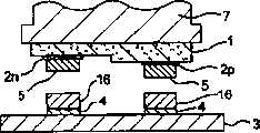
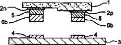
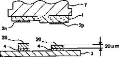
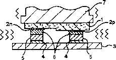
如图1所示,LED(Light Emitting Diode:发光二极管)芯片1具有大体正方形形状,在与基板的接合侧表面上形成有作为元件电极之一个实例的多个衬垫2。各衬垫2,根据LED芯片1的特性,可以分开形成为两类:一类是形成呈长圆形的P极衬垫(P型电极的一个实例)2p,另一类是形成大体呈圆形的N极衬垫(N型电极的一个实例)2n。例如,P极衬垫形成得大小为0.6mm×0.1mm左右,N极衬垫形成得大小为直径0.1mm左右。As shown in FIG. 1 , an LED (Light Emitting Diode: Light Emitting Diode)
而且图2中表示这种LED元件1的剖面示意图。如图2所示,LED元件1具有多层结构,各衬垫2形成得在设有各衬垫2的衬垫形成面中,P极衬垫2p和N极衬垫2n的形成高度(形成厚度)互相不同。各衬垫2形成高度的这差异,起因于LED芯片1的特性,例如将LED芯片1的衬垫形成面配置得处于上面的状态下,P极衬垫2p的位置处于N极衬垫2n的上方,互相之间的高度差为2微米左右。2 shows a schematic cross-sectional view of such an
此外,图3A是表示LED芯片1的剖面示意图,图3B是表示安装了在图3A中所示的LED芯片1的基板2的剖面示意图。如图3A所示,在LED芯片1的各衬垫2上形成有作为突起电极之一例的突起5。这种突起5,例如可以用电镀法由作为导电性材料一例的金(Au)形成。而且如图3B所示,大体呈平板状的基板3,作为该图示上面的LED芯片1安装面上形成有多个基板电极4。基板3的该面上的各基板电极4的配置,形成得与LED芯片1中各衬垫2的配置对应(一致)。通过这样形成和配置各衬垫2和基板电极4,能够使LED芯片1的各衬垫借助于各突起5接合在基板3的各基板电极4上。其中,本发明中的基板,包括硅(Si)晶片、树脂基板、纸-苯酚基板、陶瓷基板、玻璃·环氧(glaepo)基板、薄膜基板等电路基板,单层基板或多层基板等电路基板,部件、筐体或薄膜等,形成电路的物品。3A is a schematic cross-sectional view showing the
然而在这种LED芯片1中,如上所述,通过使P极衬垫2p和N极衬垫2n之间的形成高度互相不同,用上述电镀法形成的各突起5的顶端高度位置,也因上述形成高度不同而变得不同。即使在这种各衬垫2的形成高度不同的情况下,也不会受该差异的影响,以下利用图4A、图4B、图4C、图4D、图4E和图4F所示的LED芯片1和基板3的示意剖面图,就将LED芯片1安装在基板3上的安装方法说明如下。However, in this
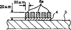
首先如图4A所示,在LED芯片1的P极衬垫2p和N极衬垫2n的上面,例如以电镀法用金形成突起(金突起)5。P极衬垫2p和N极衬垫2n,例如虽然有2微米左右的形成高度差,但是利用电镀法形成各突起5时,要使各突起5的形成高度不同是困难的,所以各突起5被形成为形成高度大体相同。因此,如图4A所示,在P极衬垫2p上形成的突起5的图示顶端高度位置,与在N极衬垫2n上形成的突起5的图示顶端高度位置将变得互相不同,其差别例如为2微米左右。First, as shown in FIG. 4A , on the
接着,或者与上述各突起形成工序并行地、向安装了LED芯片1的基板3的各基板电极4的图示上面,利用涂布或者印刷办法供给作为糊状导电性材料一例的金纳米糊料(也是金属纳米糊料的一例),形成作为接合部件一例的多个接合电极6。另外,有时也可以在形成这种接合电极6之前,对基板3的各基板电极4实施等离子体洗涤处理。在这种情况下,能够使各基板电极4的表面处于清洁状态下,能够使各基板电极4的表面与向该表面供给的金纳米糊料之间的接触性更加良好的缘故。Then, or in parallel with the above-mentioned each protrusion forming process, on the surface of each
这里所述的“金纳米糊料”,如图4C所示,是指作为由金形成的超微金颗粒的多个金微粒(导电性微粒)9a和添加成分9b(例如含有粘接成分或各种添加剂等,每种成分不一定仅限于具有导电性的情况)形成的糊状导电性材料。而且金糊料是一种具备在外力作用下能使其形状(形态)容易发生变化的这种塑性特性的柔软材料。The "gold nanopaste" described here, as shown in Figure 4C, refers to a plurality of gold particles (conductive particles) 9a and additional components 9b (such as containing adhesive components or Various additives, etc., each component is not necessarily limited to the case of having conductivity) to form a paste-like conductive material. Furthermore, gold paste is a soft material having such plastic properties that its shape (morphology) can be easily changed under the action of external force.
其中金糊料,在其原有的状态下具有极为柔软的特性,其硬度和粘度不能稳定地保持其形状,而且仅靠施加外力就能使其形状发生很大变化。这种柔软特性虽然适于采用涂布和印刷办法,但是从其形状的稳定性这一观点来看,有必要进行一些处理。因此,本发明的第一种实施方式中,通过对由涂布和印刷供给状态的金纳米糊料赋予能量,例如赋予热、超声波或电子热等能量,促进添加成分9b的积极挥发,使单个金纳米微粒9a之间的距离靠近,或者促进金纳米微粒9a之间的接合,与上述供给状态相比其硬度等提高,形成接合电极6。例如,对于金纳米糊料赋予上述能量时,能使金属薄膜化。这样形成的接合电极6,将具有的硬度和粘度即使不施加外力也能稳定地保持其形状的程度,而且将具有这样一种塑性(即比供给后状态下的金纳米糊料更稳定状态的塑性),当一端施加积极的外力的情况下,也能够使其形状容易发生变化,停止施加该外力的情况下,能够保持其变形后的形状。因此,也可以将这种赋予能量的处理,叫作对金纳米糊料的稳定化处理。Among them, gold paste is extremely soft in its original state, its hardness and viscosity cannot maintain its shape stably, and its shape can be greatly changed only by applying external force. This soft property is suitable for coating and printing methods, but some processing is necessary from the viewpoint of shape stability. Therefore, in the first embodiment of the present invention, the active volatilization of the added component 9b is promoted by imparting energy, such as heat, ultrasonic waves, or electron heat, to the gold nano paste in the state supplied by coating and printing, so that individual The distance between the gold nanoparticles 9a is close, or the bonding between the gold nanoparticles 9a is promoted, and the hardness thereof is increased compared with the supply state described above, and the
在此,将用图17A、图17B、图17C和图17D示意表示的剖面图,详细说明对这种金纳米糊料赋予能量的稳定化处理的机理。Here, the mechanism of the stabilization treatment for imparting energy to this gold nanopaste will be described in detail using the cross-sectional views schematically shown in FIGS. 17A , 17B, 17C, and 17D.
首先如图17A所示,金纳米糊料由多个金纳米微粒9a和添加成分9b构成。作为这种添加成分9b,例如可以使用与单个金纳米微粒9a不互相熔融粘着,能以单个存在的分散剂(以下叫作分散9b),如图17A所示,单个金纳米微粒9a的表面处于被分散剂9b包覆的状态下,并处于互相独立存在的状态下。这里将这种独立存在的金纳米微粒9a叫作独立分散的纳米微粒。First, as shown in FIG. 17A, the gold nanopaste is composed of a plurality of gold nanoparticles 9a and additive components 9b. As this additional component 9b, for example, a dispersant (hereinafter referred to as dispersion 9b) that does not melt and adhere to each other with a single gold nanoparticle 9a can be used alone. As shown in FIG. 17A, the surface of a single gold nanoparticle 9a is at In the state of being coated with the dispersant 9b, and in the state of being independent of each other. Such independently-existing gold nanoparticles 9a are referred to herein as independently dispersed nanoparticles.
一旦对这种状态下的金纳米糊料赋予热或电子射线等能量,如图17B所示,覆盖各金纳米微粒9a表面的分散剂9b就从金纳米微粒9a的表面剥离,然后气化蒸发。通过使分散剂9b这样剥离,各金纳米微粒9a的稀有(洁净)的外表面就会露出,其结果如图17C所示,位置处于附近的各金纳米微粒9a之间就开始熔融粘着。When energy such as heat or electron beams is applied to the gold nanopaste in this state, as shown in FIG. 17B, the dispersant 9b covering the surface of each gold nanoparticle 9a is peeled off from the surface of the gold nanoparticle 9a, and then gasified and evaporated. . By peeling off the dispersant 9b in this way, the rare (clean) outer surface of each gold nanoparticle 9a is exposed. As a result, as shown in FIG.
这种熔融粘着作用一旦得到促进,如图17D所示,多个金纳米微粒9a之间互相熔合,形成比原来的金纳米微粒9a更大的金微粒9c。由此,具有柔软特性的金纳米糊料,形成金块(固体)的状态。而且,可以将这一系列机理叫作金纳米糊料的烧结机理。Once this fusion adhesion is promoted, as shown in FIG. 17D, a plurality of gold nanoparticles 9a are fused with each other to form gold particles 9c that are larger than the original gold nanoparticles 9a. As a result, the gold nanopaste having a soft property is in the state of a gold nugget (solid). Moreover, this series of mechanisms can be called the sintering mechanism of the gold nanopaste.
另外,在本第一种实施方式中,对于通过这种金纳米糊料的固体化,即通过进行稳定化处理而形成的接合电极6而言,需要具有对其施加外力下容易变形的特性,但是当赋予上述能量时,通过设定能量强度或赋予时间等条件,能够获得上述特性。In addition, in the first embodiment, the
而且上述金纳米糊料的涂布或印刷等的具体办法,例如有用丝网和刮浆板供给金纳米糊料的方法,和用喷墨方式等供给金纳米糊料的方法等。而且通过上述电镀法形成的各突起5的形成高度不同,若采用这种金纳米糊料供给方法,由于能够精确控制金纳米糊料的供给量,所以能够在将其形成高度控制得很小的情况下形成各接合电极6。其中各接合电极6的形成高度(厚度),例如可以定为20微米左右。而且考虑到在LED芯片1的LED芯片1的各P极衬垫2p和N极衬垫2n上形成的突起5的顶端高度位置的差异,可以调整金纳米糊料在基板3的各基板电极4上的供给量,可以使接合电极6形成得各形成高度(厚度)互相不同。也就是说,如图4D所示,在使各衬垫2与各基板电极4的位置互相吻合的状态下,将LED芯片1在基板3的上方配置得互相大体平行(即大体呈水平状态)的状态下,根据LED芯片1的各突起5的顶端高度位置的差异,根据各突起5的顶端与基板3的各基板电极4之间距离的差别,决定各形成厚度形成各接合电极6。也就是说,考虑到形成在P极衬垫2p上的突起5的顶端与基板电极4之间的距离,比形成在N极衬垫2n上的突起5的顶端与基板电极4之间的距离短,所以各接合电极6形成得:被配置在P极衬垫2p的突起5与基板电极4之间的接合电极6的形成厚度,与被配置在N极衬垫2n的突起5与基板电极4之间的接合电极6的形成厚度相比,相互的距离的差别减小。而且,作为对上述金纳米糊料稳定化处理,并不限于上述那样赋予能量的情况,例如也可以采用仅将金纳米糊料放置所定时间的方式进行该稳定化处理。即使在这种情况下,也能促进金纳米糊料中所含的添加成分9b的蒸发,在使各金纳米微粒9a更紧密接触的同时,提高接合电极6的导电性。但是从能够缩短安装时间的观点,和能够迅速保持由涂布和印刷法形成的形状的观点来看,优选采用以能量赋予的方式进行积极的稳定化处理。Furthermore, specific methods of coating or printing the above-mentioned gold nanopaste include, for example, a method of supplying the gold nanopaste with a screen or a squeegee, and a method of supplying the gold nanopaste by an inkjet method or the like. And the formation height of each
然后如图4D所示,对LED芯片1与基板3的上述位置进行吻合。这种位置吻合,例如利用作为部件保持部件一例的吸附嘴7的保持面7a,将作为形成了LED芯片1的衬垫2的衬垫形成面反面的被吸附面1a(图示的上面)一边保持,一边使被互相大体平行配置的状态下的LED芯片1与基板3作相对移动,通过使各衬垫2与各基板电极4的位置互相吻合的方式进行。Then, as shown in FIG. 4D , match the aforementioned positions of the
进行这种位置吻合之后,如图4E所示,使吸附嘴7下降,借助于各接合1电极6使LED芯片1的各突起5的顶端与基板3的各基板电极4对接。这种对接时,根据各突起5的顶端与各基板电极4之间距离尺寸上的差别,形成着各厚度尺寸不同的接合电极6,所以各突起5的顶端大体同时与各接合电极6对接。因此,LED芯片1与基板3保持在互相平行的状态下,进行上述对接。这种对接之后,使吸附嘴7停止下降,保持该对接状态。其中各接合电极6,有时也可以利用由金纳米糊料形成,具有柔软的性质,经过上述对接之后,使吸附嘴7进一步仅下降微小距离,将各突起5压紧(加压),使各接合电极6产生微小变形。在这种情况下,由其在形成精度上的误差,即使使各突起5的形成高度各异,使各接合电极6产生微小变形,能确保各突起5与各接合电极6之间具有充分接触面积,实现可靠的对接。After such positioning, as shown in FIG. 4E , the
然后如图4E所示,保持这种对接的状态下,通过吸附嘴7对LED芯片1赋予超声波振动。这种超声波振动,将被传递到各衬垫2、突起5、接合电极6和基板电极4上。通过赋予这种超声波振动,在处于互相加压的对接状态下的各突起5的顶端与各接合电极6的上面,将被削出未被有机物等污染的新生面,进而各新生面之间互相胶合,形成金属接合的状态。而且如上所述,由于能够确保各突起5与各接合电极6之间具有充分的接触面积而处于可靠的对接状态下,所以这种金属接合在各突起5中大体同时进行。另外,这种超声波振动由吸附嘴7的赋予,因为能够可靠进行上述金属接合,所以仅仅赋予所定时间。Then, as shown in FIG. 4E , ultrasonic vibration is applied to the
通过这样实施金属接合,借助于各突起5和各接合电极6使LED芯片1的各衬垫2接合在基板3的各基板电极4上。然后接触由吸附嘴7对LED芯片1的吸附保持状态,同时使吸附嘴7上升。这样可以将LED芯片1安装在基板3上,制成作为半导体元件安装基板一例的LED芯片安装基板10。其中如图4F所示,在LED芯片1中形成各衬垫2的面与基板3中形成有基板电极3的面之间,注入作为绝缘材料一例的密封材料,形成密封部分8后进行密封处理,也可以可靠地对LED芯片1与基板3的接合部件进行保护。By performing metal bonding in this way, each
另外,在上述中,作为糊状导电性材料,虽然例如是以采用金纳米糊料的情况作了说明,但是本第一种实施方式并不仅限于这种情况。也可以代替金使用银(AG)纳米糊料。银纳米糊料与金纳米糊料相比具有价格低廉的优点。但是银纳米糊料与金纳米糊料相比更容易被氧化,而且也容易产生迁移,所以在要求更稳定更可靠和更高精度接合的情况下,优选采用金纳米糊料。In addition, in the above, as the paste-like conductive material, for example, the case of using gold nanopaste has been described, but the first embodiment is not limited to this case. Silver (AG) nanopaste can also be used instead of gold. Silver nanopaste has the advantage of being inexpensive compared to gold nanopaste. However, silver nano paste is easier to be oxidized and migrated than gold nano paste, so it is preferred to use gold nano paste when more stable, reliable and high-precision bonding is required.
而且在上述中,虽然是就在各基板电极4的上面形成一个接合电极4的情况加以说明的,但是本第一种实施方式并不仅仅限于这种情况。也可以例如如图6所示的基板电极4的剖面放大图所示,在一个基板电极4的上面形成多个接合电极6a,以便形成多个突起。这种情况下,对于各接合电极6a的形成高度而言,由于能够使形成宽度更小,所以通过对各接合电极6a赋予超声波振动,能够制成更容易变形的形状(长宽比)。因此,能够缩短因赋予超声波振动而接合所需的时间,同时由于具有更容易进行上述变形的形状,所以能够进行更加稳定而可靠的接合。其中,这种各接合电极6a的形成,能够采用金纳米糊料例如以喷墨方式等印刷来形成。而且各接合电极6a,例如能以20微米左右的形成宽度和20微米左右的形成高度形成。其中,各接合电极6a的形成间隔(形成间距)应当根据其接合状态设定最佳值。In the above, although the case where one
此外在上述中,虽然是就在基板3的各基板电极4的上面形成各接合电极6的情况进行说明的,但是本第一种实施方式并不仅仅限于这种情况。也可以代替这种情况,例如如图7所示,在LED芯片1上的各突起5上形成各接合电极6。即使在这种情况下,也能不变地借助于各突起5和接合电极6b使各衬垫2对接在各基板电极4上。In addition, in the above, although the case where the
而且例如代替利用电镀法在LED芯片1的各衬垫2上形成各突起5, 如图15A和图15B所示,也可以在基板3的各基板电极4上形成各突起5,然后通过赋予超声波振动进行接合。对于各衬垫2的形成高度各异的LED芯片1而言,在搅拌机3中由于各基板电极4的形成高度大体均匀,所以具有能用电镀法有效地形成各突起的优点。此外,如图16A和图16B所示,有时也可以在LED芯片1的各衬垫2上和基板3的各基板电极4上这二者上形成各突起5A、5B。And, for example, instead of forming the
根据上述第一种实施方式能够获得以下各种效果。According to the first embodiment described above, the following various effects can be obtained.
首先利用电镀法在LED芯片1的各衬垫2上形成的各突起5,其硬度高达80~90HV左右,而且基板3的各基板电极4的硬度也高达70~90HV左右,所以在二者互相对接的状态下仅仅赋予超声波振动很难使突起崩溃,很难实施充分的金属间接合,与此相比,对作为柔软材料的糊状导电性材料的金糊料赋予能量时,将由生成的金属膜形成的接合电极6配置在各突起5与各基板电极4之间,使硬度比上述各硬度低得多的各接合电极6处于其间,使各突起5与各基板电极4对接的情况下赋予超声波振动,能够进行充分的金属间接合。First, the hardness of each
也就是说在该对接之时,将比突起5等柔软的各接合电极6压入各突起5与基板电极4之间,通过使之产生微小的变形,使各接合电极6处于各突起5与各基板电极4之间,能够进行可靠地对接。而且在这种对接之时,在各突起5与各接合电极6的对接部分,能够确保充分的接合面积(接触面积)。在这种状态下赋予超声波能量时,在上述充分的接合面积上具有可靠而充分的接合强度,能够进行金属接合,进行稳定的接合。而且由于在各突起5与各基板电极4之间插入用相同材料形成的各接合电极6,所以能使各突起5与基板电极4之间的接合条件相同。因此,由于能够使处于各突起5与基板电极4之间的接合电极6同时进行接合,所以能够将因一部分突起等首先接合等而产生的应力集中现象防患于未然,因而能够进行更高精度和稳定的接合。That is, at the time of the mating, each
而且对于用电镀法形成的各突起5而言,虽然有时因其形成精度而使形成高度各异,但是即使在存在这种形成高度差异的情况下,由于各接合电极6是用作为柔软材料的金纳米糊料形成的,所以各接合电极6不但能吸收各突起5在形成高度上的波动,而且通过使各接合电极6处于各突起5与基板电极4之间而能够使其可靠地对接,经过赋予超声波振动能够进行可靠而稳定的接合。Furthermore, although the
另外,为了保持其形状,对于具有过分柔软这一特性的金纳米糊料而言,利用涂布和印刷法将其供给之后,以赋予能量的方式进行稳定化处理的情况下,能够稳定地保持其形状,实现可靠而稳定的接合。这种稳定化处理,无需使用特殊的药液等,通过赋予热、超声波或电子射线等能量的方式就能进行,所以能够特别迅速而可靠地进行处理。In addition, in order to maintain its shape, the gold nanopaste that has the characteristic of being too soft can be stably maintained when it is supplied by coating and printing methods and then stabilized by applying energy. Its shape enables a reliable and stable joint. Such stabilization treatment can be performed by applying energy such as heat, ultrasonic waves, or electron beams without using a special chemical solution, so it can be performed particularly quickly and reliably.
此外这样借助于各接合电极6使各突起5在基板电极4上可靠处于对接状态,通过赋予超声波振动,能够使各突起5的顶端与各接合电极6大体同时接合,而且能够缩短该接合所需的时间。因此,能够将不以大体同时进行接合以及延长接合所需时间而带来的接合不良现象防患于未然。In addition, each
而且通过赋予能量由金纳米糊料形成的各接合电极6,由于具有比突起5等相比其硬度显著低和柔软的特性,所以不会使硬度高的突起5因赋予超声波振动而产生应力集中,能使突起5产生裂纹的问题的产生减少。Furthermore, each
而且根据在具有P极衬垫2p和N极衬垫2n的形成高度不同这一特征的LED芯片1上形成的各突起5的顶端,与基板3的各基板电极4之间距离尺寸上的差异,调整金纳米糊料的供给量的情况下,形成各接合电极6使各厚度尺寸不同,利用这种方式处置P极衬垫2p和N极衬垫2n在形成高度上的差异,能够可靠而稳定地进行安装。也就是说,即使当各衬垫2的形成高度存在这种差异的情况下,也能用各接合电极6调整该差异,能够在确保LED芯片1与基板3之间的水平度的情况下,进行LED芯片1的安装。And according to the difference in the distance dimension between the top of each
而且在这种接合电极6形成时,利用柔软糊状材料的这一特性,借助于涂布或印刷等办法对金纳米糊料的供给能够在控制其微小供给量的情况下进行,所以能够可靠地进行上述厚度尺寸的控制。And when this
这样使用金纳米糊料能够实现超声波接合(金属接合),所以其容许温度处于200℃以下,其容许温度比焊锡的熔点238℃低,在不使焊锡再流动的情况下就能将具有耐热性差这一特征的LED芯片1安装在基板3上。因此,能够将已有的焊锡类流动时因热和产生气体而使LED芯片1受到损伤的现象防患于未然。而且也无需伴随使用焊锡而需要的助熔剂供给工序和洗涤工序,能够节省时间和人力,能够提高安装效率。与此同时,还能适应近年来的环境要求。In this way, the use of gold nano paste can realize ultrasonic bonding (metal bonding), so its allowable temperature is below 200°C, and its allowable temperature is lower than the melting point of solder at 238°C. It can be heat-resistant without reflowing the solder. The
因此,根据上述第一种实施方式的安装方法,为使伴随着对LED芯片1施加电压而产生的热量向基板3侧散热,而以大尺寸形成各衬垫2、突起5、和基板电极4,在使用接合电极6的情况下,通过有效地赋予充分的超声波振动,而且在缩短该振动的赋予时间的情况下,能够可靠而有效地对这些各衬垫2、突起5、和基板电极4进行互相接合。Therefore, according to the mounting method of the above-mentioned first embodiment, in order to dissipate the heat generated by applying a voltage to the
(第二种实施方式)(Second implementation mode)
另外,本发明并不限于上述实施方式,能够采用其他各种实施方式实施。例如,本发明的第二种实施方式涉及的作为半导体元件的安装方法之一例的LED芯片1的安装方法,将用图5所示的示意说明图加以说明。其中关于与上述第一种实施方式中的LED芯片1和基板3具有相同构成部分,为了便于说明和理解将赋予相同的参照符号。In addition, the present invention is not limited to the above-described embodiments, and can be implemented in other various embodiments. For example, a method of mounting an
首先如图5A所示,在LED芯片1的上面,与上述第一种实施方式同样,在各衬垫2的上面形成突起5。这种各突起5,例如可以采用电镀法由金形成。而且LED芯片1的P极衬垫2p和N极衬垫2n由于在形成高度上不同(例如形成高度相差2微米),所以在形成的各突起5的顶端高度位置上也存在同样程度上的高度差别。First, as shown in FIG. 5A , on the upper surface of the
而且如图5B所示,利用涂布或印刷的办法向基板3中的各基板电极4的图示上面供给金纳米糊料,形成各接合电极16。这样形成各接合电极16,与上述第一种实施方式的情况不同,其形成厚度处于大体均匀的状态下,例如形成具有20微米左右的形成厚度。此外,通过对这样供给的金纳米糊料赋予所定的能量,在其形状可以实现稳定化的状态下,形成各接合电极16。Furthermore, as shown in FIG. 5B , the gold nanopaste is supplied to the upper surface of each
然后如图5C所示,利用吸附嘴7吸附保持未形成LED芯片1的各衬垫2一侧的表面,将其配置在基板3的上方,沿着基板3的表面上能够互相接合的方向使LED芯片1的各衬垫2和基板3的各基板电极4进行位置吻合。Then, as shown in FIG. 5C , the surfaces on one side of the
这种位置吻合之后,通过使吸附嘴7下降使LED芯片1下降,使LED芯片1的各突起5的顶端与各接合电极16对接。此时如上所述,由于各突起5的顶端高度位置互相不同,所以在P极衬垫2p上形成的突起5,比在N极衬垫2n上形成的突起5更先与接合电极16对接。这种对接之后,继续使吸附嘴7微小地下降,使处于该对接状态下的上述接合电极16被在P极衬垫2p上形成的突起5加压变形。通过这样使上述接合电极16变形,能够使尚未处于接合状态下的在N极衬垫2n上形成的突起5进一步下降,如图5D所示,能够使该突起5与接合电极16对接。在保持这种对接状态下,即保持各接合电极16与各突起5接触受压的状态下,停止吸附嘴7的下降动作。After such alignment, the
然后如图5D所示,一边保持这种对接状态,一边用吸附嘴7对LED芯片1赋予所定时间的超声波振动。通过赋予这种超声波振动,能够使处于互相加压对接状态下的各突起5的端面与各接合电极16的上面互相胶合,形成金属接合的状态。Then, as shown in FIG. 5D , ultrasonic vibration is applied to the
通过这样实施金属接合,LED芯片1的各衬垫2通过各突起5和各接合电极16而处于与基板3的各基板电极4的接合状态下。然后在解除由吸附嘴7对LED芯片1的吸附保持状态的同时,使吸附嘴7上升。这样就如图5E所示,就能将LED芯片1安装在基板3上。By performing metal bonding in this way, each
根据上述第二种实施方式,正如上述第一种实施方式那样,即使没有根据LED芯片1中P极衬垫2p和N极衬垫2n形成高度上的不同使各突起5顶端高度位置上产生的差别,使各接合电极16的形成厚度形成各异的情况下,利用各接合电极16是作为糊状导电性材料的金纳米糊料形成的柔软的(比突起5等柔软)特性,也根据各突起5的形成高度用突起5对接合电极16加压使其变形的情况下,能够吸收各突起5顶端高度位置上的差异。According to the above-mentioned second embodiment, just like the above-mentioned first embodiment, even if there is no difference in the formation height of the P-
因此,即使在各衬垫2的形成高度和各突起5的形成高度存在这种差别的情况下,通过使接合电极16变形能够进行可靠的对接。而且在这种可靠对接的状态下,通过赋予超声波能量,能够使各突起5与各接合电极16可靠地进行金属接合,通过赋予超声波振动,能够将LED芯片1可靠地安装在基板3上。Therefore, even in the case where there is such a difference in the formation height of each
而且采用这种安装方法,像LED芯片1那样,并不限于事先对P极衬垫2p和N极衬垫2n在形成高度上的差别进行判断的情况,也能用于各衬垫和突起因其形成精度而产生的形成高度波动的情况,因此可以说是一种适用范围更广的安装方法。And adopting this mounting method, like the
(第三种实施方式)(the third implementation mode)
以下利用图8A、图8B和图8C所示的示意说明图,对本发明的第三种实施方式涉及的半导体元件安装方法之一例的LED芯片1的安装方法进行说明。其中关于与上述第一种实施方式中的LED芯片1和基板3具有相同构成部分,为了便于说明和理解将赋予相同的参照符号。Hereinafter, the mounting method of the
本第三种实施方式的安装方法中,并不像上述第一种实施方式和第二种实施方式的安装方法那样,利用电镀法在LED芯片1的各衬垫2上形成突起,借助于该各突起将LED芯片1安装在基板3上,而是在不形成各突起的情况下进行安装的。In the mounting method of the third embodiment, unlike the mounting methods of the above-mentioned first embodiment and the second embodiment, protrusions are formed on the
首先如图8A所示,用涂布或印刷办法向基板3的各基板电极4的上面供给金纳米糊料,形成各接合电极26。此时与第一种实施方式中的安装方法同样,根据LED芯片1的P极衬垫2p和N极衬垫2n在形成高度上的差异,对金纳米糊料的供给量进行微小调整,同时使各接合电极26的厚度尺寸不同,以此方式形成各接合电极26。其中当上述各接合电极26形成时,通过对供给的金纳米糊料赋予所定能量,将使其形成的形状稳定化。First, as shown in FIG. 8A , gold nanopaste is supplied onto the upper surface of each
然后如图8A所示,利用吸附嘴7吸附保持未形成LED芯片1的各衬垫2一侧的表面,将其配置在基板3的上方,沿着基板3的表面能够互相接合的方向使LED芯片1的各衬垫2和基板3的各基板电极4进行位置吻合。Then, as shown in FIG. 8A , the surfaces of the
这种位置吻合之后,通过吸附嘴7下降使LED芯片1下降,使LED芯片1的各衬垫2与各接合电极26对接。此时,LED芯片1中的各衬垫2在形成高度上虽然不同,但是由于根据这种不同在基板3中形成各接合电极26,所以P极衬垫2p与接合电极26对接,以及N极衬垫2n与接合电极26对接的过程大体同时进行。在保持这种对接的状态下使吸附嘴7的下降动作停止。在这种对接状态下,各接合电极26可以保持与各衬垫2接触受压的状态。After matching the positions, the
然后如图8B所示,一边保持这种对接状态,一边利用吸附嘴7对LED芯片1赋予所定时间的超声波振动。通过赋予这种超声波振动,能够使处于互相加压对接状态下的各衬垫2的表面与各接合电极26的上面互相胶合,形成金属接合的状态。Then, as shown in FIG. 8B , ultrasonic vibration is applied to the
通过这样实施金属接合,LED芯片1的各衬垫2将通过各接合电极26而处于接合在基板3的各基板电极4上的状态下。然后,在解除由吸附嘴7对LED芯片1的吸附保持状态的同时,使吸附嘴7上升。这样如图8C所示,LED芯片1将被安装在基板3上。By performing metal bonding in this way, each
而且,在上述中,虽然是就在基板3的各基板电极4上形成接合电极26的情况加以说明的,但是也可以代之以在LED芯片1的各衬垫2上形成接合电极26。无论在哪种情况下,都能够使各接合电极26处于其间,使各衬垫2与基板电极4进行对接的缘故。In addition, above, although the case where the
根据上述第三种实施方式,并不像上述第一种实施方式和上述第二种实施方式,通过电镀法等在LED芯片1的各衬垫上,或者在基板3的各基板电极4上形成各突起5,而是在不形成各突起的情况下,借助于各接合电极26使各衬垫2与各基板电极4对接的状态下,通过赋予超声波振动,能够使处于各衬垫2与基板电极4之间的接合电极26进行接合。According to the above-mentioned third embodiment, unlike the above-mentioned first embodiment and the above-mentioned second embodiment, the electrode is formed on each pad of the
对于这种安装方法而言,由于并不伴随用电镀法所需的突起形成工序,所以可以省略该工序所需的时间和人力,能提供一种效率更高的安装方法。Since this mounting method does not involve the process of forming protrusions required by the electroplating method, the time and manpower required for this process can be omitted, and a more efficient mounting method can be provided.
以下利用图9所示以往的超声波接合方法的示意说明图,说明上述各实施方式中赋予超声波振动中接合(超声波接合)所需的一般条件。Hereinafter, general conditions required for bonding (ultrasonic bonding) in which ultrasonic vibration is imparted in each of the above-described embodiments will be described using a schematic explanatory diagram of a conventional ultrasonic bonding method shown in FIG. 9 .
在图9所示的传统的超声波接合方法中,在被吸附嘴510所吸附保持的半导体元件501的各元件电极502上形成的各突起505,在作为所定垂直荷重的接合荷重加压对接的状态下,利用吸附嘴510赋予超声波振动而进行超声波接合。此时,将吸附嘴510的半导体元件501的保持面与半导体元件501的图示的上面之间的摩擦系数定为μ1,将互相处于对接状态的突起505与基板电极504之间的摩擦系数定为μ2,将基板503与保持此基板503的台架520之间的摩擦系数定为μ3。In the conventional ultrasonic bonding method shown in FIG. 9 , each
在这种超声波接合中,为了实施理想的超声波接合,应当确保(μ3F>μ3F>μ2F)的条件。也就是说,通过用吸附嘴510赋予超声波振动,希望可以将上述超声波振动有效地传递到各突起505与基板电极504的对接部分,而不希望将超声波振动更多地传递到吸附嘴510的保持面与半导体元件501之间,或基板3与台架520之间。例如,在(μ2F>μ1F)的条件中,与各突起505与基板电极504的对接部分相比,在吸附嘴510的保持面与半导体元件501之间将被更多地赋予超声波振动。这种情况下,吸附嘴510与半导体元件501之间将发生横向滑动,将会出现不能进行超声波接合的情况。In such ultrasonic bonding, in order to implement ideal ultrasonic bonding, the condition (μ3F>μ3F>μ2F) should be ensured. That is to say, by imparting ultrasonic vibrations with the suction nozzle 510, it is hoped that the above-mentioned ultrasonic vibrations can be effectively transmitted to the abutting portion of each
与此相比,在本发明的上述各实施方式涉及的安装方法中,在LED芯片1的各衬垫2与基板3的各基板电极4之间,处于夹持因赋予所定能量而得到稳定化处理的金纳米糊料所形成的接合电极的状态下,因超声波振动的赋予而能使超声波振动更多地集中在作为最软部分的各接合电极上。因而能够提供一种可以将吸附嘴的横向滑动或对LED芯片1及突起等的损伤等现象防患于未然的、由赋予超声波振动而接合的方法。In contrast, in the mounting methods according to the above-mentioned embodiments of the present invention, between the
而且在上述各实施方式中,虽然是就在LED芯片1的各衬垫2、各突起5或基板3的各基板电极4上供给金纳米糊料,在需要的位置形成各接合电极的情况进行说明的,但是本发明并不仅仅限于这种情况。除了这种情况之外,也可以是例如事先用金纳米糊料和绝缘材料,形成在绝缘片中配置了由金纳米糊料形成的接合电极的片材,对这种片材中形成的接合电极与LED芯片1的衬垫2和基板3的基板电极4进行位置吻合,使上述片材中的接合电极处于LED芯片1的衬垫与基板3的基板电极4之间加以对接。通过在这种对接状态下赋予超声波振动,能够使上述片材中的接合电极处于衬垫2与基板电极4之间而接合。而且与此同时,也可以通过上述片材中的绝缘材料对该对接部分周围进行密封的密封处理。Moreover, in each of the above-mentioned embodiments, although the gold nanopaste is supplied on each
此外在上述实施方式中,虽然是就半导体元件是LED芯片1的情况为主而加以说明的,但是半导体元件并不仅限于这种情况。可以说,半导体元件只要是能借助于元件电极安装在基板上的,与半导体元件的功能无关,都能采用本发明的安装方法。而且就在这种半导体元件中形成的元件电极而言,无论形成多个还是一个,各种情况下都能采用本发明的安装方法。In addition, in the above-mentioned embodiment, although the case where the semiconductor element is the
而且这里作为LED芯片1在基板上实际安装状态的一个实例,图14中示出LED芯片1在基板3上安装状态下接合部件的剖面放大图。如图14所示,事先在LED芯片1的衬垫2上形成突起5,而且在基板3上用金纳米糊料形成有电极布线36。通过在将突起5的下端对接在电极布线上的状态下赋予超声波振动,使突起5的下端表面,和与其接触的电极布线36的表面被金属接合,以此方式进行上述安装。其中,突起5形成的尺寸为50微米×50微米。14 shows an enlarged cross-sectional view of a bonding member in a state in which the
此外在上述实施方式中,虽然是就由金纳米糊料形成的各接合电极6实施超声波振动处理,而进行超声波接合的情况进行说明的,但是采用这种接合电极6的接合方法并不仅限于这种情况。例如也可以代之以这种情况,即在不伴随赋予超声波振动的情况下,在用各衬垫2和据初步统计电极4夹持各接合电极6的情况下加压,使其形状变形,使各衬垫2和各基板电极4夹持各接合电极6的情况下对接,以此方式进行接合。其中在这种对接之后,既可以采用对各接合电极6加热,然后使其冷却固化,在这种情况下进行上述接合,或者也可以采用将各接合电极6放置,使其自然固化的情况下进行上述接合。In addition, in the above-mentioned embodiment, although the case where ultrasonic vibration treatment is performed on each of the
另外,通过对上述各种实施方式中任何实施形态进行适当组合,也能产生各自具有的效果。In addition, by appropriately combining any of the various embodiments described above, the respective effects can be produced.
本发明虽然是参照附图就与实施方式有关的内容进行充分说明的,但是对于本领域普通技术人员来说显然可以作出各种变形或修改。这种变形或修改只要落入本发明的技术方式的范围之内,也应当理解为被包含在其中。Although the present invention has been fully described regarding the embodiments with reference to the drawings, it is obvious to those skilled in the art that various changes and modifications can be made. As long as such deformation or modification falls within the scope of the technical method of the present invention, it should also be understood as being included therein.
2003年10月7日提出的申请号为No.2003-347977日本专利申请的说明书、附图和权利要求中所公开的内容,全部以参照方式并入本说明书之中。The contents disclosed in the description, drawings and claims of Japanese Patent Application No. 2003-347977 filed on October 7, 2003 are hereby incorporated by reference in their entirety.
Claims (19)
Translated fromChineseApplications Claiming Priority (2)
| Application Number | Priority Date | Filing Date | Title |
|---|---|---|---|
| JP2003347977 | 2003-10-07 | ||
| JP2003347977 | 2003-10-07 |
Publications (2)
| Publication Number | Publication Date |
|---|---|
| CN1606143Atrue CN1606143A (en) | 2005-04-13 |
| CN100437961C CN100437961C (en) | 2008-11-26 |
Family
ID=34587151
Family Applications (1)
| Application Number | Title | Priority Date | Filing Date |
|---|---|---|---|
| CNB2004100849768AExpired - Fee RelatedCN100437961C (en) | 2003-10-07 | 2004-10-08 | Semiconductor element mounting method and mounting substrate |
Country Status (3)
| Country | Link |
|---|---|
| US (1) | US20050110161A1 (en) |
| CN (1) | CN100437961C (en) |
| TW (1) | TW200520123A (en) |
Cited By (3)
| Publication number | Priority date | Publication date | Assignee | Title |
|---|---|---|---|---|
| CN102918664A (en)* | 2010-08-26 | 2013-02-06 | 夏普株式会社 | Mounting method for semiconductor light emitter |
| CN105870312A (en)* | 2010-06-29 | 2016-08-17 | 柯立芝照明有限公司 | Electronic devices with yielding substrates |
| CN110556350A (en)* | 2018-05-30 | 2019-12-10 | 夏普株式会社 | Semiconductor chip laminate and method for manufacturing semiconductor chip laminate |
Families Citing this family (38)
| Publication number | Priority date | Publication date | Assignee | Title |
|---|---|---|---|---|
| CN100394571C (en)* | 2003-05-20 | 2008-06-11 | 富士通株式会社 | Testing method of LSI package and LSI element and manufacturing method of semiconductor device |
| KR101025844B1 (en)* | 2003-10-01 | 2011-03-30 | 삼성전자주식회사 | SnAgAb solder bumps, a method of manufacturing the same and a light emitting device bonding method using the method |
| US20060234405A1 (en)* | 2005-04-13 | 2006-10-19 | Best Scott C | Semiconductor device with self-aligning contactless interface |
| KR20080037681A (en)* | 2005-08-23 | 2008-04-30 | 로무 가부시키가이샤 | Semiconductor chip, manufacturing method thereof, and semiconductor device |
| JP2007173363A (en)* | 2005-12-20 | 2007-07-05 | Fujitsu Ltd | Flying lead joining method |
| JP2007173362A (en)* | 2005-12-20 | 2007-07-05 | Fujitsu Ltd | Flying lead joining method |
| JP2007172697A (en) | 2005-12-20 | 2007-07-05 | Fujitsu Ltd | Flying lead joining method |
| JP4638382B2 (en)* | 2006-06-05 | 2011-02-23 | 田中貴金属工業株式会社 | Joining method |
| WO2008147394A1 (en)* | 2006-11-08 | 2008-12-04 | Northeastern University | Three dimensional nanoscale circuit interconnect and method of assembly by dielectrophoresis |
| KR100881183B1 (en)* | 2006-11-21 | 2009-02-05 | 삼성전자주식회사 | Semiconductor chip having bumps of different heights and semiconductor package including the same |
| JP4361572B2 (en)* | 2007-02-28 | 2009-11-11 | 株式会社新川 | Bonding apparatus and method |
| JP5363839B2 (en)* | 2008-05-12 | 2013-12-11 | 田中貴金属工業株式会社 | Bump, method for forming bump, and method for mounting substrate on which bump is formed |
| WO2009157160A1 (en)* | 2008-06-25 | 2009-12-30 | パナソニック株式会社 | Packaging structure and method for manufacturing packaging structure |
| US7754533B2 (en)* | 2008-08-28 | 2010-07-13 | Infineon Technologies Ag | Method of manufacturing a semiconductor device |
| US8384114B2 (en) | 2009-06-27 | 2013-02-26 | Cooledge Lighting Inc. | High efficiency LEDs and LED lamps |
| US8637379B2 (en)* | 2009-10-08 | 2014-01-28 | Infineon Technologies Ag | Device including a semiconductor chip and a carrier and fabrication method |
| US8653539B2 (en) | 2010-01-04 | 2014-02-18 | Cooledge Lighting, Inc. | Failure mitigation in arrays of light-emitting devices |
| US8493000B2 (en) | 2010-01-04 | 2013-07-23 | Cooledge Lighting Inc. | Method and system for driving light emitting elements |
| JP5481249B2 (en)* | 2010-03-26 | 2014-04-23 | 富士通株式会社 | Semiconductor device and manufacturing method thereof |
| WO2012000114A1 (en) | 2010-06-29 | 2012-01-05 | Cooledge Lightning Inc. | Electronic devices with yielding substrates |
| JP2012069545A (en) | 2010-09-21 | 2012-04-05 | Toyoda Gosei Co Ltd | Method for mounting light-emitting element |
| EP2639841B1 (en)* | 2010-11-11 | 2019-07-24 | Nichia Corporation | Light-emitting device, and method for manufacturing circuit board |
| TWI447409B (en)* | 2010-12-31 | 2014-08-01 | Advanced Optoelectronic Tech | Led package structure detect device and the method of detecting the same |
| US9231178B2 (en) | 2012-06-07 | 2016-01-05 | Cooledge Lighting, Inc. | Wafer-level flip chip device packages and related methods |
| US8970035B2 (en)* | 2012-08-31 | 2015-03-03 | Taiwan Semiconductor Manufacturing Company, Ltd. | Bump structures for semiconductor package |
| JP6143104B2 (en)* | 2012-12-05 | 2017-06-07 | 株式会社村田製作所 | Bumped electronic component and method for manufacturing bumped electronic component |
| DE102013104407B4 (en)* | 2013-04-30 | 2020-06-18 | Tdk Corporation | Device that can be produced at wafer level and method for producing it |
| JP6433590B2 (en)* | 2015-06-11 | 2018-12-05 | 三菱電機株式会社 | Power semiconductor device manufacturing method and power semiconductor device |
| US20170309549A1 (en)* | 2016-04-21 | 2017-10-26 | Texas Instruments Incorporated | Sintered Metal Flip Chip Joints |
| JP6556105B2 (en)* | 2016-07-28 | 2019-08-07 | 太陽誘電株式会社 | Manufacturing method of electronic device |
| US11024608B2 (en) | 2017-03-28 | 2021-06-01 | X Display Company Technology Limited | Structures and methods for electrical connection of micro-devices and substrates |
| JP6942589B2 (en)* | 2017-09-27 | 2021-09-29 | 旭化成株式会社 | Semiconductor light emitting device and ultraviolet light emitting module |
| JP7100980B2 (en)* | 2018-01-22 | 2022-07-14 | ローム株式会社 | LED package |
| US11101417B2 (en) | 2019-08-06 | 2021-08-24 | X Display Company Technology Limited | Structures and methods for electrically connecting printed components |
| KR102788934B1 (en)* | 2019-12-06 | 2025-03-31 | 삼성디스플레이 주식회사 | Method for aligning a light emitting element, method for fabricating a display device using the same and display device |
| US11581280B2 (en)* | 2019-12-27 | 2023-02-14 | Stmicroelectronics Pte Ltd | WLCSP package with different solder volumes |
| JP7491769B2 (en) | 2020-08-04 | 2024-05-28 | 株式会社ジャパンディスプレイ | Circuit board, LED module, display device, and method for manufacturing LED module and method for manufacturing display device |
| CN115188779B (en)* | 2022-07-12 | 2025-09-12 | 苏州华星光电技术有限公司 | A CMOS image chip, camera and debugging method thereof |
Family Cites Families (24)
| Publication number | Priority date | Publication date | Assignee | Title |
|---|---|---|---|---|
| JPS5357481A (en)* | 1976-11-04 | 1978-05-24 | Canon Inc | Connecting process |
| US5001542A (en)* | 1988-12-05 | 1991-03-19 | Hitachi Chemical Company | Composition for circuit connection, method for connection using the same, and connected structure of semiconductor chips |
| US5173256A (en)* | 1989-08-03 | 1992-12-22 | International Business Machines Corporation | Liquid metal matrix thermal paste |
| JP3297254B2 (en)* | 1995-07-05 | 2002-07-02 | 株式会社東芝 | Semiconductor package and manufacturing method thereof |
| US5882722A (en)* | 1995-07-12 | 1999-03-16 | Partnerships Limited, Inc. | Electrical conductors formed from mixtures of metal powders and metallo-organic decompositions compounds |
| JP2751912B2 (en)* | 1996-03-28 | 1998-05-18 | 日本電気株式会社 | Semiconductor device and manufacturing method thereof |
| JP3610999B2 (en)* | 1996-06-07 | 2005-01-19 | 松下電器産業株式会社 | Mounting method of semiconductor element |
| DE69830883T2 (en)* | 1997-03-10 | 2006-04-20 | Seiko Epson Corp. | Semiconductor device and equipped with this device circuit board |
| US5783465A (en)* | 1997-04-03 | 1998-07-21 | Lucent Technologies Inc. | Compliant bump technology |
| US6238599B1 (en)* | 1997-06-18 | 2001-05-29 | International Business Machines Corporation | High conductivity, high strength, lead-free, low cost, electrically conducting materials and applications |
| US6337522B1 (en)* | 1997-07-10 | 2002-01-08 | International Business Machines Corporation | Structure employing electrically conductive adhesives |
| US5969461A (en)* | 1998-04-08 | 1999-10-19 | Cts Corporation | Surface acoustic wave device package and method |
| US6087021A (en)* | 1998-05-28 | 2000-07-11 | International Business Machines Corporation | Polymer with transient liquid phase bondable particles |
| JP2000068327A (en)* | 1998-08-20 | 2000-03-03 | Matsushita Electric Ind Co Ltd | Component mounting method and equipment |
| JP3678048B2 (en)* | 1999-04-05 | 2005-08-03 | 松下電器産業株式会社 | Solder precoat method and solder precoat substrate |
| JP3451373B2 (en)* | 1999-11-24 | 2003-09-29 | オムロン株式会社 | Manufacturing method of data carrier capable of reading electromagnetic wave |
| JP2001217380A (en)* | 2000-02-04 | 2001-08-10 | Hitachi Ltd | Semiconductor device and method of manufacturing the same |
| US6346750B1 (en)* | 2000-04-28 | 2002-02-12 | Micron Technology, Inc. | Resistance-reducing conductive adhesives for attachment of electronic components |
| JP2002050716A (en)* | 2000-08-02 | 2002-02-15 | Dainippon Printing Co Ltd | Semiconductor device and manufacturing method thereof |
| US6576493B1 (en)* | 2000-10-13 | 2003-06-10 | Bridge Semiconductor Corporation | Method of connecting a conductive trace and an insulative base to a semiconductor chip using multiple etch steps |
| JP2002151551A (en)* | 2000-11-10 | 2002-05-24 | Hitachi Ltd | Flip-chip mounting structure, semiconductor device therewith and mounting method |
| JP4051893B2 (en)* | 2001-04-18 | 2008-02-27 | 株式会社日立製作所 | Electronics |
| TW558809B (en)* | 2002-06-19 | 2003-10-21 | Univ Nat Central | Flip chip package and process of making the same |
| JP3819851B2 (en)* | 2003-01-29 | 2006-09-13 | 松下電器産業株式会社 | Semiconductor device and manufacturing method thereof |
- 2004
- 2004-10-06USUS10/958,246patent/US20050110161A1/ennot_activeAbandoned
- 2004-10-06TWTW093130219Apatent/TW200520123A/enunknown
- 2004-10-08CNCNB2004100849768Apatent/CN100437961C/ennot_activeExpired - Fee Related
Cited By (4)
| Publication number | Priority date | Publication date | Assignee | Title |
|---|---|---|---|---|
| CN105870312A (en)* | 2010-06-29 | 2016-08-17 | 柯立芝照明有限公司 | Electronic devices with yielding substrates |
| CN102918664A (en)* | 2010-08-26 | 2013-02-06 | 夏普株式会社 | Mounting method for semiconductor light emitter |
| CN102918664B (en)* | 2010-08-26 | 2015-04-15 | 夏普株式会社 | Mounting method for semiconductor light emitter |
| CN110556350A (en)* | 2018-05-30 | 2019-12-10 | 夏普株式会社 | Semiconductor chip laminate and method for manufacturing semiconductor chip laminate |
Also Published As
| Publication number | Publication date |
|---|---|
| CN100437961C (en) | 2008-11-26 |
| US20050110161A1 (en) | 2005-05-26 |
| TW200520123A (en) | 2005-06-16 |
Similar Documents
| Publication | Publication Date | Title |
|---|---|---|
| CN1606143A (en) | Semiconductor element mounting method and mounting substrate | |
| CN1161834C (en) | Semiconductor device and manufacturing method thereof | |
| CN1303677C (en) | Circuit board, mounting structure of semiconductor element with bumps, and electro-optical device | |
| CN1269612C (en) | Solder foil, semiconductor devices, electronic devices, semiconductor components and power components | |
| JP4246134B2 (en) | Semiconductor element mounting method and semiconductor element mounting substrate | |
| CN1076872C (en) | Chip carrier and method of manufacturing and mounting the same | |
| CN1497709A (en) | Circuit substrate, installation structure of solder ball grid array and electro-optical device | |
| CN1160780C (en) | Multi-layer solder sealing tape for semiconductor substrate and process thereof | |
| CN1241244C (en) | Method for mounting semiconductor element | |
| CN1280884C (en) | Semiconductor device and manufacture thereof, circuit board and electronic machine | |
| CN1790651A (en) | Manufacturing method of chip integrated substrate | |
| CN1235457C (en) | Circuit substrate and its making method and display apparatus | |
| CN1260795C (en) | Semiconductor device and manufacture thereof, circuit board and electronic machine | |
| CN1437256A (en) | Semiconductor element and its manufacturing method, and semiconductor device and its manufacturing method | |
| CN1423347A (en) | Luminance element and making method thereof and lead frame for making said element | |
| CN1585123A (en) | Flip-chip type semiconductor device and its manufacturing process and electronic product manufacturing process | |
| CN1574346A (en) | A method of manufacturing a semiconductor device | |
| CN1438825A (en) | Electro-optical device manufacturing method and manufacturing device, electro-optic device, electronic device | |
| CN1101642C (en) | Method and apparatus for producing electronic circuit device, and jig for making solder residue unifrom and transferring solder paste | |
| CN1344014A (en) | Semiconductor device and semiconductor assembly | |
| CN1655353A (en) | Laminated MCP and its manufacturing method | |
| CN1838395A (en) | Semiconductor device and manufacturing method thereof | |
| CN1340851A (en) | Electronic device and its manufacture method | |
| CN1179625A (en) | Semiconductor element and its manufacturing method, semiconductor device and its manufacturing method | |
| CN1531013A (en) | Reinforcing plate adhesion device and adhesion method |
Legal Events
| Date | Code | Title | Description |
|---|---|---|---|
| C06 | Publication | ||
| PB01 | Publication | ||
| C10 | Entry into substantive examination | ||
| SE01 | Entry into force of request for substantive examination | ||
| C14 | Grant of patent or utility model | ||
| GR01 | Patent grant | ||
| CF01 | Termination of patent right due to non-payment of annual fee | Granted publication date:20081126 Termination date:20141008 | |
| EXPY | Termination of patent right or utility model |