CN1581481A - ESD protection circuit with control circuit - Google Patents
ESD protection circuit with control circuitDownload PDFInfo
- Publication number
- CN1581481A CN1581481ACN200410056375.6ACN200410056375ACN1581481ACN 1581481 ACN1581481 ACN 1581481ACN 200410056375 ACN200410056375 ACN 200410056375ACN 1581481 ACN1581481 ACN 1581481A
- Authority
- CN
- China
- Prior art keywords
- mentioned
- circuit
- pad
- esd protection
- protection circuit
- Prior art date
- Legal status (The legal status is an assumption and is not a legal conclusion. Google has not performed a legal analysis and makes no representation as to the accuracy of the status listed.)
- Granted
Links
Images


Classifications
- H—ELECTRICITY
- H10—SEMICONDUCTOR DEVICES; ELECTRIC SOLID-STATE DEVICES NOT OTHERWISE PROVIDED FOR
- H10D—INORGANIC ELECTRIC SEMICONDUCTOR DEVICES
- H10D89/00—Aspects of integrated devices not covered by groups H10D84/00 - H10D88/00
- H10D89/60—Integrated devices comprising arrangements for electrical or thermal protection, e.g. protection circuits against electrostatic discharge [ESD]
- H10D89/601—Integrated devices comprising arrangements for electrical or thermal protection, e.g. protection circuits against electrostatic discharge [ESD] for devices having insulated gate electrodes, e.g. for IGFETs or IGBTs
- H10D89/811—Integrated devices comprising arrangements for electrical or thermal protection, e.g. protection circuits against electrostatic discharge [ESD] for devices having insulated gate electrodes, e.g. for IGFETs or IGBTs using FETs as protective elements
- H10D89/819—Bias arrangements for gate electrodes of FETs, e.g. RC networks or voltage partitioning circuits
- H—ELECTRICITY
- H01—ELECTRIC ELEMENTS
- H01L—SEMICONDUCTOR DEVICES NOT COVERED BY CLASS H10
- H01L2924/00—Indexing scheme for arrangements or methods for connecting or disconnecting semiconductor or solid-state bodies as covered by H01L24/00
- H01L2924/0001—Technical content checked by a classifier
- H01L2924/0002—Not covered by any one of groups H01L24/00, H01L24/00 and H01L2224/00
Landscapes
- Semiconductor Integrated Circuits (AREA)
- Metal-Oxide And Bipolar Metal-Oxide Semiconductor Integrated Circuits (AREA)
Abstract
Description
Translated fromChinese本申请是基于并要求日本专利申请第2003-205735号、申请日为2003年8月4日的优先权,在此通过引用而并入该专利申请的全部内容。This application is based on and claims priority from Japanese Patent Application No. 2003-205735, filed August 4, 2003, the entire contents of which are hereby incorporated by reference.
技术领域technical field
本发明涉及保护IC(Integrated Circuit,集成电路)以及LSI(Large ScaleIntegration Circuit,大规模集成电路)等半导体集成电路的不受到ESD(Electrostatic Discharge,静电放电)的影响的ESD保护电路。The present invention relates to the ESD protection circuit that the semiconductor integrated circuits such as protection IC (Integrated Circuit, integrated circuit) and LSI (Large Scale Integration Circuit, large-scale integrated circuit) are not subjected to the influence of ESD (Electrostatic Discharge, electrostatic discharge).
背景技术Background technique
以往,为了保护IC或LSI等的半导体集成电路不受ESD产生的高电压影响,而提出各种各样的ESD保护电路。这里用图1~图5来说明以往的3种ESD保护电路。Conventionally, various ESD protection circuits have been proposed in order to protect semiconductor integrated circuits such as ICs and LSIs from high voltages generated by ESD. Here, three types of conventional ESD protection circuits will be described using FIGS. 1 to 5 .
图1是模式化示意以往例1的ESD保护电路的电路图。FIG. 1 is a circuit diagram schematically showing an ESD protection circuit of Conventional Example 1. As shown in FIG.
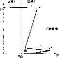
如图1所示,在第1、第2焊盘(pad)11、12上连接有内部电路13,在这些焊盘11、12之间连接有钳位电路14。上述钳位电路14由NMOS晶体管18构成。即,上述NMOS晶体管18的漏极连接于第1焊盘11,源极连接于第2焊盘12,栅极与背栅极连接于源极。As shown in FIG. 1 , an
接着用图2来说明如图1所示电路的动作。图2是模式化示意图1所示的NMOS晶体管18的电压-电流特性的图。在图2中,横轴为NMOS晶体管18的漏极与源极之间外加的电压值V1,纵轴为在漏极与源极之间流过的电流值I1。首先,在第1焊盘11与第2焊盘12之间不外加由ESD产生的高电压的情况下(区域1),作为钳位电路14的NMOS晶体管18的漏极与源极之间不流有电流。这是由于NMOS晶体管18的栅极与源极互相连接并成为相同电位,处于非导通状态(截止)。因此,当不必要保护内部电路13受到高压影响的情况下,不影响内部电路13的正常工作。Next, the operation of the circuit shown in FIG. 1 will be described using FIG. 2 . FIG. 2 is a diagram schematically showing the voltage-current characteristics of the
另一方面,在第1焊盘11与第2焊盘12之间外加由ESD产生的高电压的情况下(区域2),NMOS晶体管处于导通状态(导通),由ESD产生的ESD电荷从第1焊盘11经过钳位电路14向第2焊盘放走。即,能够不对内部电路13外加高电压从而保护内部电路13。On the other hand, when a high voltage generated by ESD is applied between the
进一步详细说明上述区域2的NMOS晶体管18的电压-电流特性。当NMOS晶体管的漏极与源极之间加有高电压时,如图2所示,一旦达到触发电压Vt1后,NMOS晶体管18就产生急速返回(snap-back)。由于上述急速返回特性,电压下降到维持电压Vh。然后,使电流急剧流出。The voltage-current characteristics of the
还有,这时流于NMOS晶体管18的电流是,从漏极经过基板部分向源极流出的作为双极性作用的截止电流。因此,不是流于NMOS晶体管18沟道部的导通电流。In addition, the current flowing in the
但是,如上结构的ESD保护电路必须满足以下2个设计条件。第1设计条件是,应保护的内部电路13的耐压值(破坏内部电路13的电压)必须高于触发电压值Vt1的耐压值。第2设计条件是,保持电压值Vh必须高于内部电路13的电源电压值Vdd。还有,上述第2设计条件是在排除内部电路13处于正常工作时钳位电路14成为导通状态(导通)的情况而求得的设计条件。However, the ESD protection circuit with the above structure must satisfy the following two design conditions. The first design condition is that the withstand voltage value of the
但是,伴随着近年来的半导体制造技术的细微化,用于内部电路的MOSFET的栅极耐压值急剧下降。例如,在0.18~0.13微处理中,触发电压值Vt1与栅极耐压值大致相同,在0.09微处理中,栅极耐压值比触发电压值Vt1要低。即,内部电路13的耐压值比触发电压值Vt1要低。因此,考虑到今后的细微化处理,很难满足上述第1设计条件。However, with recent miniaturization of semiconductor manufacturing technology, the gate withstand voltage value of MOSFETs used in internal circuits has dropped rapidly. For example, in microprocessing 0.18-0.13, the trigger voltage value Vt1 is approximately the same as the gate withstand voltage value, and in microprocess 0.09, the gate withstand voltage value is lower than the trigger voltage value Vt1. That is, the withstand voltage value of the
接着用图3以及图4来说明以往例2的ESD保护电路。图3是模式化示意以往例2的ESD保护电路的电路图。Next, the ESD protection circuit of Conventional Example 2 will be described with reference to FIGS. 3 and 4 . FIG. 3 is a circuit diagram schematically showing an ESD protection circuit of Conventional Example 2. FIG.
该以往例2的ESD保护电路是在上述以往例1所示的ESD保护电路中进一步设置有时间常数电路23。这样的ESD保护电路例如记载于美国专利6,249,410号说明书(2001年6月19日,图4)中。The ESD protection circuit of this conventional example 2 is further provided with the time
上述时间常数电路23由电容C和电阻元件R所构成。上述电容C的一方的电极连接于焊盘11,另一方的电极连接于NMOS晶体管18的栅极。上述电阻元件R的一端连接于上述NMOS晶体管的栅极,另一端连接于焊盘12。The above-mentioned time
其次,用图4来说明图3所示的ESD保护电路的动作。图4是示意图3所示的NMOS晶体管18的电压-电流特性图。在图4中,横轴为NMOS晶体管18的漏极与源极之间外加的电压值V1,纵轴为流于漏极与源极之间的电流值I1。Next, the operation of the ESD protection circuit shown in FIG. 3 will be described using FIG. 4 . FIG. 4 is a voltage-current characteristic diagram of the
首先,在第1焊盘11与第2焊盘12之间不外加由ESD产生的高电压的情况下,与上述以往例1相同,钳位电路14为非导通状态(截止)。因此,不影响内部电路13的正常工作。First, when no high voltage due to ESD is applied between the
但是,在第1焊盘11与第2焊盘12之间外加由ESD产生的高电压的情况下,时间常数电路23生成的一定时间的脉冲外加于NMOS晶体管18的栅极上。因此,NMOS晶体管处于导通状态。即,钳位电路14处于导通状态(导通)。However, when a high voltage due to ESD is applied between the
因此,由ESD产生的ESD电荷从第1焊盘11经过钳位电路14向第2焊盘12放出。因而,能够保护内部电路13不受由ESD产生的高电压的影响。还有,上述的一定时间大致由电容C的容量值和电阻元件R的电阻值相乘所得的时间常数来决定。Therefore, ESD charges generated by ESD are released from the
用图4来详细说明在上述第1焊盘11与第2焊盘12之间外加由ESD产生的高电压的情况下的NMOS晶体管18的电压-电流特性。The voltage-current characteristics of the
图4中的实线25示意流于NMOS晶体管18的沟道的电压-电路特性。即,实线25是“NMOS晶体管18导通时”的特性。进一步,图4中的虚线26表示相对于以往例1的急速返回特性的电压-电流特性。即,虚线26是“NMOS晶体管18截止时”的特性。如图4所示,实线25的特性比虚线26的特性能流出更多的电流。因此,对于ESD的保护能力比以往例1更高。还有,如上述实线25所示的特性与以往例1不同,是由流过NMOS晶体管18的源极与漏极之间形成的沟道部的导通电流所显示的特性。又,如虚线26所示的流过NMOS晶体管18的电流是作为双极性作用不流于沟道部的截止电阻。A solid line 25 in FIG. 4 shows the voltage-circuit characteristics flowing in the channel of the
可见,以往例2不是利用NMOS晶体管18的截止电流而是利用其导通电流。因此,不必考虑以往例1的第1设计条件即“触发电压Vt1必须低于应保护的内部电路的耐压(破坏内部电路的电压)1”这样的涉及条件。It can be seen that the conventional example 2 does not use the off current of the
但是,在以往例2中,时间常数电路23的设计成为难题。即,当上述时间常数(=电容C的容量值与电阻元件R的电阻值相乘的值小时,NMOS晶体管18处于导通的时间就变短,不能起到有效的ESD保护的作用。相反,当时间常数大时,NMOS晶体管18处于导通的时间就长,能起到有效的ESD保护的作用。但是,电阻元件R和电容C的尺寸越大,芯片成本就越高。而且,由于上述时间常数电路23对每一对的焊盘是必要的,导致芯片整体的制造成本增加以及芯片尺寸的大幅度增大。However, in Conventional Example 2, the design of the time
接着用图5来说明以往例3的ESD保护电路。图5是模式化示意以往例3的ESD保护电路的电路图。该ESD保护电路记载于例如ON-CHIP ESD PROTECTIONFOR INTEGATED CIRCUITS An IC Design Perspective Figure 4-24(AlbertZ.H.Wang著Kluwer Academic Publishers Group)。Next, the ESD protection circuit of Conventional Example 3 will be described with reference to FIG. 5 . FIG. 5 is a circuit diagram schematically showing an ESD protection circuit of Conventional Example 3. FIG. This ESD protection circuit is described in, for example, ON-CHIP ESD PROTECTION FOR INTEGATED CIRCUITS An IC Design Perspective Figure 4-24 (Kluwer Academic Publishers Group by Albert Z.H.Wang).
如图5所示的以往例3的ESD保护电路在时间常数电路23与钳位电路14之间依次连接有第1至第3的逆变器30-1、30-2、30-3的输入端和输出端。In the ESD protection circuit of the conventional example 3 shown in FIG. terminal and output terminal.
上述第1至第3的逆变器30-1、30-2、30-3由PMOS晶体管P-1、P-2、P-3和NMOS晶体管N-1、N-2、N-3构成。上述第1逆变器30-1的输入端连接于时间常数电路23的节点24,其输出端连接于第2逆变器30-2的输入端。上述第2逆变器30-2的输出端连接于第3逆变器30-3的输入端。上述第3逆变器30-3的输出端连接于上述钳位电路14的NMOS晶体管18的栅极。The above first to third inverters 30-1, 30-2, 30-3 are composed of PMOS transistors P-1, P-2, P-3 and NMOS transistors N-1, N-2, N-3 . The input terminal of the first inverter 30-1 is connected to the
其次来说明其动作。首先,说明在第1焊盘11与第2焊盘12之间外加由ESD产生的高电压时的动作。当在第1焊盘11与第2焊盘12之间外加高电压,由于时间常数电路23和逆变器电路30生成的信号,使作为钳位电路14的NMOS晶体管18处于导通状态。由此,外加于第1焊盘11的ESD电荷通过钳位电路14向第2焊盘12放走,以保护内部电路。其它的动作因与上述以往例2相同,故省略其说明。Next, its operation will be described. First, the operation when a high voltage due to ESD is applied between the
但是,以往例3的ESD保护电路由于使用了时间常数电路23,存在与以往例2同样的问题。又,由于设置有逆变器电路30,对芯片尺寸以及制造成本更不利。However, the ESD protection circuit of the conventional example 3 has the same problems as the conventional example 2 because the time
如上所述的以往的ESD保护电路,保护能力不充分,而且伴随着细微化,使设计以及制造更难,使制造成本增加,芯片尺寸增大。The above-mentioned conventional ESD protection circuit has insufficient protection capability, and furthermore, the design and manufacture are more difficult due to the miniaturization, which increases the manufacturing cost and increases the chip size.
发明内容Contents of the invention
本发明的ESD保护电路具备:作为与半导体集成电路连接的外部连接端的第1焊盘、作为与上述半导体集成电路连接的外部连接端的第2焊盘、连接在上述第1焊盘与第2焊盘之间的钳位电路、以及控制上述钳位电路为导通状态或非导通状态的控制电路。The ESD protection circuit of the present invention includes: a first pad as an external connection terminal connected to a semiconductor integrated circuit, a second pad as an external connection terminal connected to the semiconductor integrated circuit, and a pad connected to the first pad and the second pad. A clamping circuit between disks, and a control circuit for controlling the clamping circuit to be in a conduction state or a non-conduction state.
附图说明Description of drawings
图1是示意以往例1的ESD保护电路的电路图。FIG. 1 is a circuit diagram showing an ESD protection circuit of Conventional Example 1. As shown in FIG.
图2是示意以往例1的钳位电路的电压-电流特性图。FIG. 2 is a graph showing voltage-current characteristics of the clamp circuit of Conventional Example 1. FIG.
图3是示意以往例2的ESD保护电路的电路图。FIG. 3 is a circuit diagram showing an ESD protection circuit of Conventional Example 2. FIG.
图4是示意以往例2的钳位电路的电压-电流特性图。FIG. 4 is a graph showing voltage-current characteristics of the clamp circuit of Conventional Example 2. FIG.
图5是示意以往例3的ESD保护电路的电路图。FIG. 5 is a circuit diagram showing an ESD protection circuit of Conventional Example 3. FIG.
图6是说明本发明的ESD保护电路的概要结构的电路图。FIG. 6 is a circuit diagram illustrating a schematic configuration of the ESD protection circuit of the present invention.
图7是模式化示意图6所示的钳位电路的电压-电流特性图。FIG. 7 is a voltage-current characteristic diagram of the clamping circuit shown in the schematic diagram 6 .
图8是模式化示意本发明的第1实施方式的ESD保护电路的电路图。FIG. 8 is a circuit diagram schematically showing an ESD protection circuit according to the first embodiment of the present invention.
图9是模式化示意本发明的第2实施方式的ESD保护电路的电路图。FIG. 9 is a circuit diagram schematically showing an ESD protection circuit according to a second embodiment of the present invention.
图10是模式化示意本发明的第2实施方式的变形例的ESD保护电路的电路图。FIG. 10 is a circuit diagram schematically showing an ESD protection circuit according to a modified example of the second embodiment of the present invention.
图11是模式化示意本发明的第3实施方式的ESD保护电路的电路图。FIG. 11 is a circuit diagram schematically showing an ESD protection circuit according to a third embodiment of the present invention.
图12是模式化示意本发明的第4实施方式的ESD保护电路的电路图。FIG. 12 is a circuit diagram schematically showing an ESD protection circuit according to a fourth embodiment of the present invention.
图13是模式化示意本发明的第5实施方式的ESD保护电路的电路图。FIG. 13 is a circuit diagram schematically showing an ESD protection circuit according to a fifth embodiment of the present invention.
图14是模式化示意本发明的第6实施方式的ESD保护电路的电路图。FIG. 14 is a circuit diagram schematically showing an ESD protection circuit according to a sixth embodiment of the present invention.
具体实施方式Detailed ways
以下,参照附图来说明本发明的实施方式。还有,所有图的共同部分标有共同的参照符号。Hereinafter, embodiments of the present invention will be described with reference to the drawings. Also, parts common to all figures are marked with common reference symbols.
首先,用图6以及图7来说明本发明的ESD保护电路的概略结构。First, the schematic structure of the ESD protection circuit of this invention is demonstrated using FIG.6 and FIG.7.
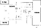
如图6所示,半导体芯片50中形成有应保护的半导体集成电路即内部电路54。进一步,第1焊盘51以及第2焊盘52与内部电路54连接,在上述第1、第2焊盘51、52之间连接有钳位电路55。又,第3焊盘53与上述控制电路56连接。上述钳位电路55根据控制电路56的输出信号来控制导通状态/非导通状态。As shown in FIG. 6 , an
接着用图7来说明图6所示的ESD保护电路的动作。图7是模式化示意图6的钳位电路55的电压-电流特性图。图7的横轴为外加于钳位电路55的电压值V,纵轴为流过钳位电路55的电流值I。进一步,图中的实线61示意第1电压-电流特性,实线62示意第2电压-电流特性。Next, the operation of the ESD protection circuit shown in FIG. 6 will be described using FIG. 7 . FIG. 7 is a voltage-current characteristic diagram of the clamping
首先,在安装LSI等的半导体芯片50之后是指,例如在电子设备以及家用电器等的终端(end)产品中作为部件组装完之后的情况。换句话说,是指在一定条件下通常工作的状态等。在该状态下,极少可能由ESD将高电压外加于内部电路54。因此,将钳位电路5设定5为第1电压-电流特性61,为非导通状态(截止状态)。First, after the semiconductor chip 50 such as LSI is mounted means, for example, a case where it is assembled as a component in end products such as electronic equipment and home appliances. In other words, it refers to a state that usually works under certain conditions, etc. In this state, there is little possibility that a high voltage will be applied to the
如上述那样安装了半导体芯片50之后,上述第3焊盘53输入用于适当地控制控制电路56的信号。由此,由于控制电路56的控制,钳位电路55的电压-电路特性为第1电压-电流特性61。如图2所示,第1电压-电流特性是当电压值V小的的情况下,没有电流值I流过的特性。即,在钳位电路54显示第1电压-电流特性61的情况下,钳位电路55处于非导通状态(截止状态)。After the semiconductor chip 50 is mounted as described above, a signal for appropriately controlling the
因此,钳位电路55的动作不会影响内部电路54的动作。因而,内部电路54能正常工作。Therefore, the operation of the
另一方面,来说明在安装半导体芯片50之前,即,在第1焊盘51与第2焊盘52之间外加有由ESD产生的高电压的情况下的动作。On the other hand, the operation in the case where a high voltage due to ESD is applied between the
在安装半导体芯片50之前是指,例如从刚制造完到在电子设备制造厂内正要往PC板上组装为止的这段时间内的状况,或者从半导体芯片在半导体工厂制造后到组装于终端产品进行通常工作为止的这段时间的状况。在以上的状况中,很有可能由ESD向内部电路54外加高电压。因此,使钳位电路55处于导通状态,无论何时都可应对由ESD产生的高电压。即,将钳位电路55控制成第2电压-电流特性62,预先设定为导通状态。由于钳位电路55处于导通状态,高电压产生的电荷经过钳位电路55,能够放电到接地电源Vss。Before the semiconductor chip 50 is mounted, it means, for example, the period from the moment it is manufactured to when it is assembled on the PC board in the electronic equipment manufacturing plant, or from the time the semiconductor chip is manufactured in the semiconductor factory to the time when it is assembled on the terminal. The condition of the product during the period of normal operation. In the above situation, there is a high possibility that a high voltage is applied to the
如上所述在安装半导体芯片50之前,虽然上述第3焊盘53没有外部信号,由于控制电路56的控制,钳位电路55的电压-电流特性为第2电压-电流特性62。如图2所示,第1电压-电流特性62的特性为,只要外加很小的电压值V就有大量的电流值I流过。即,钳位电路55在显示第2电压-电流特性62的情况下,钳位电路55处于导通状态。As mentioned above, before the semiconductor chip 50 is mounted, the voltage-current characteristic of the
因此,即使在第1焊盘51与第2焊盘52之间由ESD外加高电压(例如,数千V程度)的情况下,上述高电压也能够通过钳位电路55来放电。即,由ESD产生的ESD电荷从第1焊盘51经过钳位电路55向第2焊盘52放出。Therefore, even when a high voltage (for example, about several thousand V) is applied by ESD between the
因此,由ESD产生的高电压不外加于内部电路54。其结果,能够保护内部电路54不会受到高电压的破坏。Therefore, a high voltage generated by ESD is not applied to the
如图2所示,第2电压-电流特性62利用导通电流。因此,能够流出大量的电流,钳位电路55有很高的保护能力。As shown in FIG. 2 , the second voltage-current characteristic 62 uses a conduction current. Therefore, a large amount of current can flow, and the
进一步,利用控制电路56将钳位电路55的电压-电流特性控制成第1电压-电流特性61或者是第2电压-电流特性62。即,钳位电路55切换使用非导通状态或者是导通状态的任意一种。因此,如以往例1那样的设计条件是没有必要的。结果,不必要考虑钳位电路55设计上的限制,能够简单地制造出ESD保护电路。Furthermore, the voltage-current characteristic of the
而且,在该实施方式的ESD保护电路中也不必担心伴随着内部电路54的细微化而带来的设计条件。因此,也能够容易地应对今后的被细微化的内部电路54。Furthermore, in the ESD protection circuit of this embodiment, there is no need to worry about design conditions accompanying miniaturization of the
进一步,由于不需要时间常数电路等,能够从时间常数电路的时间常数所引起的制造上的限制中解放出来,使ESD保护电路更容易制造。还有,由于没有伴随着时间常数电路等的制造而产生的制造成本的增加以及芯片尺寸的增大,能够降低制造成本和减小芯片尺寸。Furthermore, since a time constant circuit and the like are not required, it is possible to release the restriction on manufacture due to the time constant of the time constant circuit, thereby making it easier to manufacture the ESD protection circuit. Also, since there is no increase in manufacturing cost and an increase in chip size accompanying the manufacture of a time constant circuit or the like, it is possible to reduce manufacturing cost and reduce the chip size.
(第1实施方式)(first embodiment)
用图8来说明本发明的第1实施方式的ESD保护电路。图8是模式化示意ESD保护电路的电路图。又,在以下的说明中省略与上述图6所示的ESD保护电路的说明重复部分的说明,详细说明特别不同的部分。The ESD protection circuit according to the first embodiment of the present invention will be described with reference to FIG. 8 . FIG. 8 is a circuit diagram schematically illustrating an ESD protection circuit. In addition, in the following description, the description of the part which overlaps with the description of the above-mentioned ESD protection circuit shown in FIG. 6 is omitted, and the part which differs especially is demonstrated in detail.
如图8所示,钳位电路55由开关电路65以及逆变器电路66构成,控制电路56由阻抗电路67构成,还有,第2焊盘52是接地用的焊盘,与半导体集成电路内的接地电源线连接。As shown in FIG. 8, the
上述逆变器电路66由PMOS晶体管P1以及NMOS晶体管N1构成。PMOS晶体管P1的栅极与第3焊盘53连接,源极与第1焊盘51连接,漏极与节点75连接。NMOS晶体管N1的栅极与第3焊盘53连接,源极与第2焊盘52连接,漏极与节点75连接。The above-mentioned
上述开关电路65由NMOS晶体管N2构成。上述NMOS晶体管N2的栅极连接于节点75,源极连接于第2焊盘52,漏极连接于第1焊盘51。The
上述阻抗电路67由下拉电阻元件R构成。下拉电阻元件R的一端连接于节点68,节点68与第3焊盘53连接,下拉电阻元件R的另一端连接于半导体集成电路内的接地电源线Vss。The above-mentioned
接着用图8来说明ESD保护电路的动作。在以下的动作的说明中,图7所示的钳位电路55的电压-电流特性的图示及其说明是相同的,故省略。Next, the operation of the ESD protection circuit will be described using FIG. 8 . In the following description of the operation, the illustration and description of the voltage-current characteristics of the
首先,在安装半导体芯片之后,即,在第1焊盘51与第2点整部52之间没有外加由ESD产生的高电压的状况中,上述第2点整部52与接地电源Vss连接,上述第3焊盘53与内部电源Vdd连接。First, after the semiconductor chip is mounted, that is, in the situation where the high voltage generated by ESD is not applied between the
那么,PMOS晶体管P1的栅极以及NMOS晶体管N1的栅极外加有“H(高)”电平的电压。PMOS晶体管P1处于截止状态,NMOS晶体管N1处于导通状态。Then, a voltage of "H (high)" level is applied to the gate of the PMOS transistor P1 and the gate of the NMOS transistor N1. The PMOS transistor P1 is in an off state, and the NMOS transistor N1 is in an on state.
因此,通过节点75,在NMOS晶体管N2的栅极上,外加有与第2焊盘52连接的接地电源的“L(低)”电平的电压,NMOS晶体管N2处于截止状态。Therefore, a voltage of "L (Low)" level of the ground power supply connected to the
根据以上动作,钳位电路55处于非导通状态(截止状态)。因此,钳位电路55的动作不会影响内部电路55的动作,能确保内部电路55的正常工作。According to the above operation, the
另一方面,在安装半导体芯片之前,即,在第1焊盘51与第2焊盘52之间外加由ESD产生的高电压的状况中,第3焊盘53通过阻抗电路67接地。On the other hand, before the semiconductor chip is mounted, that is, when a high voltage due to ESD is applied between the
那么,PMOS晶体管P1的栅极以及NMOS晶体管N1的栅极上外加有“L(低)”电平的电压。NMOS晶体管N1处于截止状态,PMOS晶体管P1能处于导通状态。因此,当PMOS晶体管P1处于导通状态时,NMOS晶体管N2的栅极上外加与第1焊盘51相同的电压值。Then, a voltage of "L (low)" level is applied to the gate of the PMOS transistor P1 and the gate of the NMOS transistor N1. The NMOS transistor N1 is in an off state, and the PMOS transistor P1 can be in an on state. Therefore, when the PMOS transistor P1 is turned on, the gate of the NMOS transistor N2 is supplied with the same voltage value as that of the
这时,当由ESD产生的高电压外加于第1焊盘51与第2焊盘52之间时,在PMOS晶体管P1的源极上外加有高电压,PMOS晶体管P1处于完全导通状态。因此,在NMOS晶体管N2的栅极上外加有高电压,NMOS晶体管N2处于导通状态。At this time, when a high voltage generated by ESD is applied between the
根据以上的动作,钳位电路55处于导通状态。因此,高电压通过钳位电路55放电。即,由ESD产生的ESD电荷从第1焊盘51经过钳位电路55向第2焊盘52放出。According to the above operation, the
因此,由ESD产生的高电压不外加于内部电路54上。其结果,能确保内部电路54的通常动作,以保护内部电路54。Therefore, a high voltage generated by ESD is not applied to the
如上所述,当在第1焊盘51与第2焊盘52之间外加有由ESD产生的高电压时,在NMOS晶体管N2的栅极上外加有高电压。因此,NMOS晶体管N2处于导通状态。即,该实施方式的钳位电路55利用MOS晶体管的导通电流。由于上述导通电流是流于MOS晶体管的沟道部的电流,能够流出比截止电流更多的电流。因此,对于由ESD产生的高电压,能够有效地保护内部电路54。As described above, when a high voltage due to ESD is applied between the
根据该实施方式的ESD保护电路,不仅制造容易,而且能够流出更多的电流。其它的效果,与上述图6所示的ESD保护电路相同。According to the ESD protection circuit of this embodiment, it is not only easy to manufacture, but also can flow more current. Other effects are the same as those of the above-mentioned ESD protection circuit shown in FIG. 6 .
(第2实施方式)(second embodiment)
用图9来说明第2实施方式的ESD保护电路。图9是模式化示意ESD保护电路的电路图。在以下的说明中省略与上述第1实施方式重复的部分的说明,只详细说明其不同部分。The ESD protection circuit of the second embodiment will be described with reference to FIG. 9 . FIG. 9 is a schematic circuit diagram of an ESD protection circuit. In the following description, the description of the portion overlapping with the above-mentioned first embodiment will be omitted, and only the different portion will be described in detail.
如图9所示,开关电路65由PMOS晶体管P2构成。上述PMOS晶体管P2的栅极连接于节点75,源极连接于第2焊盘52,漏极连接于第1焊盘51。阻抗电路67的下拉电阻元件R的一端连接于与第3焊盘53连接的节点68,另一端连接于半导体集成电路内的内部电源线Vdd。上述内部电源线Vdd的电压值为正极性。第2焊盘52为电源供给用的焊盘,连接于半导体集成电路内的内部电源线Vdd。As shown in FIG. 9, the
接着来说明图9所示的ESD保护电路的动作。Next, the operation of the ESD protection circuit shown in FIG. 9 will be described.
首先,在安装半导体芯片之后,即,在第1焊盘51与第2焊盘52之间没有外加由ESD产生的高电压的状况下,向第2焊盘52供给有内部电源Vdd,第3焊盘53接地。First, after the semiconductor chip is mounted, that is, under the condition that no high voltage generated by ESD is applied between the
那么,PMOS晶体管P1的栅极以及NMOS晶体管N1的栅极外加有“L”电平的电压。PMOS晶体管P1处于导通状态,NMOS晶体管N1处于截止状态。Then, a voltage of "L" level is applied to the gate of the PMOS transistor P1 and the gate of the NMOS transistor N1. The PMOS transistor P1 is in an on state, and the NMOS transistor N1 is in an off state.
因此,在通过节点75,在PMOS晶体管P2的栅极上,外加有与第2焊盘52连接的内部电源的“H”电平的电压值,PMOS晶体管P2处于截止状态。Therefore, a voltage value of "H" level of the internal power supply connected to the
根据以上的动作,钳位电路55处于非导通状态(截止状态)。因此,钳位电路55的动作不影响内部电路54的动作,能使内部电路54正常工作。According to the above operation, the
另外,在安装半导体芯片之前,即,在第1焊盘51与第2焊盘52之间外加由ESD产生的高电压的状况下,第3焊盘53通过阻抗电路67连接于内部电源Vdd。上述内部电源Vdd的电压值为正极性。Also, before the semiconductor chip is mounted, that is, when a high voltage due to ESD is applied between the
那么,在PMOS晶体管P1的栅极以及NMOS晶体管N1的栅极上外加有“H”电平的电压。由此,PMOS晶体管P1处于截止状态,NMOS晶体管N1处于导通状态。Then, a voltage of "H" level is applied to the gates of the PMOS transistor P1 and the gates of the NMOS transistor N1. Accordingly, the PMOS transistor P1 is turned off, and the NMOS transistor N1 is turned on.
因此,在PMOS晶体管P2的栅极上,外加有与第1焊盘51相同的“L”电平的电压值,PMOS晶体管P2处于导通状态。Therefore, the same "L" level voltage value as that of the
这时,当由ESD产生的高电压外加于第1焊盘51与第2焊盘52之间时,在PMOS晶体管P2的源极上外加有高电压,PMOS晶体管P2处于完全导通状态。At this time, when a high voltage generated by ESD is applied between the
根据以上动作,钳位电路55处于导通状态。因此,高电压通过钳位电路55放电,不外加于内部电路54上。According to the above operation, the
如上所述,由于在产生ESD的状况下,钳位电路55预先处于导通状态,能够流出更多的电流。As described above, since the
如上述第1实施方式以及第2实施方式所示,即使在构成钳位电路55的MOS晶体管的导电型反转的情况下,也能得到同样的效果。这样的关系,以下也相同。As shown in the above-mentioned first and second embodiments, even when the conductivity type of the MOS transistor constituting the
(第3实施方式)(third embodiment)
用图10来说明第3实施方式的ESD保护电路。图10是模式化示意第3实施方式的ESD保护电路的电路图。在以下的说明中省略与上述第1实施方式重复的部分的说明,只详细说明其不同部分。The ESD protection circuit of the third embodiment will be described with reference to FIG. 10 . FIG. 10 is a circuit diagram schematically showing an ESD protection circuit according to a third embodiment. In the following description, the description of the portion overlapping with the above-mentioned first embodiment will be omitted, and only the different portion will be described in detail.
如图10所示,开关电路65是由双极性晶体管86构成。上述双极性晶体管86的集电极连接于第1焊盘51,发射极连接于第2焊盘52,基极连接于节点75。第2焊盘52是接地用的焊盘,连接于半导体集成电路内的接地电源线。As shown in FIG. 10 , the
接着来说明图10所示的ESD保护电路的动作。Next, the operation of the ESD protection circuit shown in FIG. 10 will be described.
首先,在安装半导体芯片之后,即,在第1焊盘51与第2焊盘52之间没有外加由ESD产生的高电压的状况下,在上述第2焊盘52上连接接地电源Vss,上述第3焊盘53连接于内部电源Vdd。First, after the semiconductor chip is mounted, that is, under the condition that no high voltage due to ESD is applied between the
那么,根据与上述实施方式相同的动作,NMOS晶体管N1处于导通状态。因此,由于在双极性晶体管86的发射极和基极上外加有同等电压,双极性晶体管86处于截止状态。Then, the NMOS transistor N1 is turned on by the same operation as in the above-mentioned embodiment. Therefore, since the same voltage is applied to the emitter and the base of the bipolar transistor 86, the bipolar transistor 86 is turned off.
因此,由于钳位电路55处于非导通状态,不影响内部电路54的动作。其结果,能使内部电路54正常工作。Therefore, since the
另外,在安装半导体芯片之前,即,在第1焊盘51与第2焊盘52之间外加由ESD产生的高电压的状况下,第3焊盘53通过阻抗电路67连接于接地电源Vss。Also, before the semiconductor chip is mounted, that is, when a high voltage due to ESD is applied between the
那么,根据与上述实施方式相同的动作,PMOS晶体管P1处于导通状态。这时,当由ESD产生的高电压外加于第1焊盘51与第2焊盘52之间时,通过第1焊盘51在PMOS晶体管P1的源极上外加有高电压,PMOS晶体管P1处于完全导通状态。因此,在双极性晶体管86的基极上外加有高电压。另外在双极性晶体管86的发射极上通过第2焊盘52外加有接地电压Vss。因此,双极性晶体管86处于导通状态。Then, the PMOS transistor P1 is turned on by the same operation as in the above-mentioned embodiment. At this time, when the high voltage generated by ESD is applied between the
根据以上动作,钳位电路55处于导通状态。因此,高电压通过钳位电路55放电,由ESD产生的ESD电荷从第1焊盘51经过钳位电路55向第2焊盘52放电。其结果,能够保护内部电路54不受到高电压的影响。According to the above operation, the
一般地说,双极性晶体管与MOS晶体管相比,动作速度更快,能流出更多的电流。其结果,能进一步提高钳位电路55的电压-电流特性。Generally speaking, bipolar transistors operate faster and can flow more current than MOS transistors. As a result, the voltage-current characteristics of the
(变形例)(Modification)
用图11来说明上述第2实施方式的变形例的ESD保护电路。该变形例的ESD保护电路不同于第2实施方式的电路之处在于,开关电路65是由PNP型双极性晶体管87构成。An ESD protection circuit according to a modified example of the second embodiment described above will be described with reference to FIG. 11 . The ESD protection circuit of this modified example is different from the circuit of the second embodiment in that the
即,PNP型双极性晶体管87的集电极连接于第1焊盘51,发射极连接于第2焊盘52,基极连接于节点75。第2焊盘52是电源供给用的焊盘,与半导体集成电路内的内部电源线Vdd连接。That is, the collector of the PNP type bipolar transistor 87 is connected to the
其它的结构、动作与图9、图10所示的ESD保护电路相同。Other structures and operations are the same as those of the ESD protection circuit shown in FIGS. 9 and 10 .
根据以上结构,能得到与第2实施方式相同的效果。According to the above configuration, the same effect as that of the second embodiment can be obtained.
(第4实施方式)(fourth embodiment)
用图12来说明第4实施方式的ESD保护电路。图12是模式化示意ESD保护电路的电路图。在以下的说明中省略与上述第1实施方式重复的部分的说明,只详细说明其不同部分。The ESD protection circuit of the fourth embodiment will be described with reference to FIG. 12 . FIG. 12 is a schematic circuit diagram of an ESD protection circuit. In the following description, the description of the portion overlapping with the above-mentioned first embodiment will be omitted, and only the different portion will be described in detail.
如图12所示,开关电路65是由可控硅整流电路90以及触发电路91构成的。上述可控硅整流电路90由双极性晶体管92以及双极性晶体管95构成,上述触发电路91由NMOS晶体管N2以及电阻元件99构成。As shown in FIG. 12 , the
上述双极性晶体管92的发射极连接于第1焊盘51,基极连接于双极性晶体管95的集电极,集电极连接于节点97。上述双极性晶体管95的基极连接于节点97,发射极连接于第2焊盘52。The emitter of the
上述电阻元件99的一端连接于节点97,另一端连接于第2焊盘52。第2焊盘52是接地用的焊盘,连接于半导体集成电路内的接地电源线Vss。One end of the
接着来说明图12所示的ESD保护电路。Next, the ESD protection circuit shown in FIG. 12 will be described.
首先,在安装半导体芯片之后,即,在第1焊盘51与第2焊盘52之间没有外加由ESD产生的高电压的状况下,上述第2焊盘上连接有接地电源Vss,上述第3焊盘53与内部电源Vdd连接。First, after the semiconductor chip is mounted, that is, under the condition that no high voltage generated by ESD is applied between the
那么,根据与上述实施方式相同的动作,NMOS晶体管N1处于导通状态。由此,在NMOS晶体管N2的栅极上,通过第2焊盘52外加有“L”电平的电压值。因此,NMOS晶体管N2处于截止状态。那么,由于在节点97上,外加有“L”电平的电压值,可控硅整流电路90处于截止状态。Then, the NMOS transistor N1 is turned on by the same operation as in the above-mentioned embodiment. Accordingly, a voltage value of "L" level is applied to the gate of the NMOS transistor N2 through the
如上所述,由于钳位电路55处于非导通状态,不影响内部电路54的动作。其结果,能使内部电路54正常工作。As described above, since the
另外,在安装半导体芯片之前,即,在第1焊盘51与第2焊盘52之间外加由ESD产生的高电压的状况下,第3焊盘53通过阻抗电路67接地。In addition, before the semiconductor chip is mounted, that is, when a high voltage due to ESD is applied between the
那么,根据与上述实施方式相同的动作,PMOS晶体管P1处于导通状态。这时,当由ESD产生的高电压外加于第1焊盘51与第2焊盘52之间时,通过第1焊盘51在PMOS晶体管P1的源极上外加高电压,PMOS晶体管P1处于完全导通状态。因此,在NMOS晶体管N2的栅极上也外加有高电压,NMOS晶体管N2处于导通状态。Then, the PMOS transistor P1 is turned on by the same operation as in the above-mentioned embodiment. At this time, when the high voltage generated by ESD is applied between the
接着,通过NMOS晶体管N2,由ESD产生的高电压外加于双极性晶体管95的基极上。另一方面,在双极性晶体管95的发射极上通过第2焊盘52由接地电源Vss外加“L”电平的电压。因此,双极性晶体管95处于导通状态。Next, the high voltage generated by ESD is applied to the base of the
进一步,通过双极性晶体管95,在双极性晶体管92的基极上由接地电压Vss外加“L”电平的电压。另外,在双极性晶体管92的发射极上外加由ESD产生的高电压。因此,双极性晶体管92处于导通状态。Further, a voltage of “L” level is applied from the ground voltage Vss to the base of the
根据以上动作,钳位电路55处于导通状态。因此,由ESD产生的高电压外加于钳位电路55上,不会加于内部电路54上。即,由ESD产生的ESD电荷通过可控硅整流电路90向第2焊盘52放走。其结果,能保护内部电路54。According to the above operation, the
如上所述,由于在可控硅整流电路90之间外加有高电压,能够保护内部电路54不受高电压影响。这里,一般地说,有上述结构的可控硅整流电路90能够流出比MOS晶体管更多量的电流。因此,为了流出比上述实施方式更多量的电流,能够在较小的面积中流出更多量的电流。其结果,能减小芯片尺寸。As described above, since a high voltage is applied between the thyristor rectifier circuits 90, the
(第5实施方式)(fifth embodiment)
用图13来说明第5实施方式的ESD保护电路。图13是模式化示意第5实施方式的ESD保护电路的电路图。在以下的说明中省略与上述第1实施方式重复的部分的说明,只详细说明其不同部分。The ESD protection circuit of the fifth embodiment will be described with reference to FIG. 13 . FIG. 13 is a circuit diagram schematically showing an ESD protection circuit according to a fifth embodiment. In the following description, the description of the portion overlapping with the above-mentioned first embodiment will be omitted, and only the different portion will be described in detail.
如图13所示,控制电路56由熔丝电路100构成。上述熔丝电路100由熔丝F、电阻元件R1以及电阻元件R2构成。As shown in FIG. 13 , the
上述熔丝F的一端连接于连接第4焊盘101的节点103,另一端连接于连接第5焊盘102的节点104。电阻元件R1的一端连接于内部电源Vdd,另一端连接于节点103。电阻元件R2的一端连接于接地电源Vss,另一端连接于节点104。与上述实施方式相同,第2焊盘52是接地用的焊盘,连接于半导体集成电路内的接地电源线Vss。One end of the fuse F is connected to a node 103 connected to the fourth pad 101 , and the other end is connected to a node 104 connected to the fifth pad 102 . One end of the resistance element R1 is connected to the internal power supply Vdd, and the other end is connected to the node 103 . One end of the resistance element R2 is connected to the ground power supply Vss, and the other end is connected to the node 104 . As in the above-described embodiment, the
接着来说明图13所示的ESD保护电路的动作。Next, the operation of the ESD protection circuit shown in FIG. 13 will be described.
首先,在安装半导体芯片之前,即,在第1焊盘51与第2焊盘52之间外加由ESD产生的高电压的状况下,熔丝F是连接着的。这里,在安装半导体芯片之前是指,例如LSI等半导体芯片从工厂出货的状况等。在上述状况下,由于处于外加有ESD的状况,熔丝原样地连接着,使钳位电路55处于导通状态。First, the fuse F is connected before the semiconductor chip is mounted, that is, when a high voltage due to ESD is applied between the
由于熔丝如此原样地连接着,节点103与节点104导通。又,由于Vdd是开放的,在节点103以及节点104上,外加有“L”电平的电压,NMOS晶体管N1处于截止状态,PMOS晶体管P1处于导通状态。Since the fuse is connected as it is, the node 103 and the node 104 are electrically connected. Also, since Vdd is open, a voltage of "L" level is applied to the nodes 103 and 104, the NMOS transistor N1 is turned off, and the PMOS transistor P1 is turned on.
在该状态中,当由ESD产生的高电压外加于第1焊盘51与第2焊盘52之间时,在PMOS晶体管P1的源极上施加高电压,PMOS晶体管P1处于完全导通状态。进一步,由于高电压外加于NMOS晶体管N2的栅极上,NMOS晶体管N2处于导通状态。In this state, when a high voltage generated by ESD is applied between the
根据以上的动作,钳位电路55处于导通状态,高电压通过钳位电路55外加于第1焊盘51与第2焊盘52之间,不加于内部电路54上。其结果,能够保护内部电路54不受到ESD产生的高电压的影响。According to the above operation, the
另一方面,在安装半导体芯片之后,即,在第1焊盘51与第2焊盘52之间没有外加由ESD产生的高电压的状况下,熔丝F被溶断。这里,在安装半导体芯片之后是指,例如LSI等半导体芯片组装于插板(board)后的状况等。在该状况下,外加ESD的可能性极小。因此,可在第4焊盘101与第5焊盘102之间外加高电压使熔丝溶断,使钳位电路55处于非导通状态。On the other hand, after mounting the semiconductor chip, that is, under the condition that no high voltage due to ESD is applied between the
由于熔丝F被溶断,在节点103上外加有“H”电平的电压,在PMOS晶体管P1的栅极与NMOS晶体管N1的栅极上外加有“H”电平的电压。因此,PMOS晶体管P1处于截止状态,NMOS晶体管N1处于导通状态。进一步地,在NMOS晶体管N2的栅极上通过第2焊盘52外加有“L”电平的电压。因此,NMOS晶体管N2处于截止状态。Since the fuse F is blown, a voltage of "H" level is applied to the node 103, and a voltage of "H" level is applied to the gates of the PMOS transistor P1 and the NMOS transistor N1. Therefore, the PMOS transistor P1 is in an off state, and the NMOS transistor N1 is in an on state. Furthermore, a voltage of “L” level is applied to the gate of the NMOS transistor N2 via the
根据以上动作,由于钳位电路55处于非导通状态,不影响内部电路54的动作。其结果,能使内部电路54正常工作。According to the above operation, since the
上述第1至第4的实施方式的控制电路中,在半导体芯片安装后的实际使用时,必须从控制电路的外部即第3焊盘53施加常时电压。但是,该第5实施方式的控制电路56中,熔丝切断后,不必一直在第4焊盘101以及第5焊盘102上外加电压。因此,能容易地操纵控制电路56。In the control circuits of the above-mentioned first to fourth embodiments, it is necessary to apply a constant voltage from the outside of the control circuit, that is, the
还有,作为上述实施方式中的控制电路56的一实施方式,示有阻抗电路56以及熔丝电路100。但是,控制电路56的实施方式不只限于这些,可以是将对应于是否安装有半导体芯片的数据编程的可编程序电路。In addition, the
作为上述可编程序电路的一例,例如有非易失性存储器等。进一步,在内部电路54中含有非易失性存储器的情况下,能够与内部电路54一同组入。因此,能降低制造成本,使制造得以简化。As an example of the said programmable circuit, there exist a nonvolatile memory etc., for example. Furthermore, when the
(第6实施方式)(sixth embodiment)
用图14来说明第6实施方式的ESD保护电路。图14是模式化示意ESD保护电路的电路图。在以下的说明中省略与上述实施方式重复的部分的说明,只详细说明其不同部分。The ESD protection circuit of the sixth embodiment will be described with reference to FIG. 14 . FIG. 14 is a schematic circuit diagram of an ESD protection circuit. In the following description, the description of parts overlapping with the above-mentioned embodiment will be omitted, and only the different parts will be described in detail.
在上述第1至第5实施方式中,虽然举例说明了一对第1焊盘51以及第2焊盘52与内部电路54连接的情况,实际上,多个焊盘与内部电路54连接。In the first to fifth embodiments described above, the case where the pair of
即,如图8所示,在围绕着内部电路54的4边的外部端上分别连接有多个焊盘(只代表性地表示第1焊盘51以及第2焊盘52)。在上述第1焊盘与第2焊盘之间,分别连接有钳位电路55。上述各个钳位电路55由单一的控制电路56来控制其电压-电流特性。进一步,控制电路与第3焊盘53连接。That is, as shown in FIG. 8 , a plurality of pads (only the
如图14所示的ESD保护电路的动作,因与上述实施方式的相同,故省略其说明。The operation of the ESD protection circuit shown in FIG. 14 is the same as that of the above-mentioned embodiment, so its description is omitted.
如上所述,在围绕着内部电路54的4边的外部端上,分别连接有多个焊盘,在第1焊盘与第2焊盘之间分别连接有钳位电路55。因此,当连接于4边的外部端上的焊盘的任何一个外加有由ESD产生的高电压时,高电压只加在钳位电路55上,不加于内部电路54上,其结果,能保护内部电路54。As described above, a plurality of pads are respectively connected to the outer ends surrounding the four sides of the
进一步,如上的各个钳位电路55由单一的控制电路56来控制其电压-电流特性。因此,在采用多个钳位电路55的情况下,也不必增加新的控制电路56,能降低制造成本。Further, each clamping
还有,在上述实施方式中,钳位电路55是用MOS晶体管、双极性晶体管、可控硅等的元件来说明的。但是,作为实施方式,可不只限于上述的元件,也可以是开关元件,用该开关元件响应来自控制电路56的控制信号,控制导通/截止状态,使钳位电路55处于导通状态或者是非导通状态。In addition, in the above-described embodiment, the
还有,用电源电压检测电路来构成控制电路56,当内部电路54外加有电源电压时将钳位电路55控制为处于非导通状态,当不外加电源电压时将钳位电路55控制为处于导通状态。In addition, the
本发明领域的技术人员能够容易地实现本发明的其他优点以及修改。而且,本发明范围并不限于上述详细说明以及实施形态。因此,在不背离本发明的精神以及所附权利要求的基础上,能够进行各种各样的变换。Other advantages as well as modifications of the invention will be readily apparent to those skilled in the art of the invention. In addition, the scope of the present invention is not limited to the above-mentioned detailed description and embodiment. Therefore, various changes can be made without departing from the spirit of the invention and the appended claims.
Claims (18)
Applications Claiming Priority (2)
| Application Number | Priority Date | Filing Date | Title |
|---|---|---|---|
| JP2003205735AJP4000096B2 (en) | 2003-08-04 | 2003-08-04 | ESD protection circuit |
| JP2003205735 | 2003-08-04 |
Publications (2)
| Publication Number | Publication Date |
|---|---|
| CN1581481Atrue CN1581481A (en) | 2005-02-16 |
| CN100359685C CN100359685C (en) | 2008-01-02 |
Family
ID=34113677
Family Applications (1)
| Application Number | Title | Priority Date | Filing Date |
|---|---|---|---|
| CNB2004100563756AExpired - Fee RelatedCN100359685C (en) | 2003-08-04 | 2004-08-04 | ESD protection circuit with control circuit |
Country Status (4)
| Country | Link |
|---|---|
| US (1) | US6980408B2 (en) |
| JP (1) | JP4000096B2 (en) |
| CN (1) | CN100359685C (en) |
| TW (1) | TWI282617B (en) |
Cited By (5)
| Publication number | Priority date | Publication date | Assignee | Title |
|---|---|---|---|---|
| CN101964518A (en)* | 2009-07-23 | 2011-02-02 | 天钰科技股份有限公司 | Electrostatic protection device |
| CN102055179A (en)* | 2009-11-04 | 2011-05-11 | 上海宏力半导体制造有限公司 | Electrostatic discharge protection device |
| CN101517671B (en)* | 2005-09-19 | 2013-04-10 | 加州大学评议会 | Esd protection circuits |
| CN105009285A (en)* | 2013-03-11 | 2015-10-28 | 高通股份有限公司 | Devices and methods for calibrating and operating a snapback clamp circuit |
| CN109286181A (en)* | 2017-07-21 | 2019-01-29 | 上海韦玏微电子有限公司 | Power clamp ESD protective circuit |
Families Citing this family (24)
| Publication number | Priority date | Publication date | Assignee | Title |
|---|---|---|---|---|
| WO2004102664A1 (en)* | 2003-05-13 | 2004-11-25 | Fujitsu Limited | Fuse circuit and semiconductor integrated circuit device |
| TWI281740B (en)* | 2004-09-08 | 2007-05-21 | Winbond Electronics Corp | Electrostatic discharge protection circuit |
| JP2006294903A (en)* | 2005-04-12 | 2006-10-26 | Nec Electronics Corp | Fuse trimming circuit |
| JP4913376B2 (en)* | 2005-08-22 | 2012-04-11 | ローム株式会社 | Semiconductor integrated circuit device |
| JP4562674B2 (en)* | 2006-03-23 | 2010-10-13 | 川崎マイクロエレクトロニクス株式会社 | ESD protection circuit |
| US7511931B2 (en)* | 2006-08-01 | 2009-03-31 | Intersil Americas Inc. | Self protecting output stage |
| JP4723443B2 (en)* | 2006-09-13 | 2011-07-13 | Okiセミコンダクタ株式会社 | Semiconductor integrated circuit |
| JP2008177491A (en)* | 2007-01-22 | 2008-07-31 | Renesas Technology Corp | Semiconductor device |
| US7804669B2 (en)* | 2007-04-19 | 2010-09-28 | Qualcomm Incorporated | Stacked ESD protection circuit having reduced trigger voltage |
| US8310275B2 (en)* | 2008-03-27 | 2012-11-13 | Agere Systems Inc. | High voltage tolerant input/output interface circuit |
| JP4783442B2 (en)* | 2009-03-18 | 2011-09-28 | 株式会社東芝 | ESD protection verification apparatus and ESD protection verification method |
| JP5724623B2 (en)* | 2011-05-23 | 2015-05-27 | ソニー株式会社 | Signal transmission device and imaging display system |
| US8730626B2 (en)* | 2011-10-04 | 2014-05-20 | Taiwan Semiconductor Manufacturing Company, Ltd. | Electrostatic discharge protection |
| JP5743850B2 (en)* | 2011-10-28 | 2015-07-01 | 株式会社東芝 | Integrated circuit |
| US9337644B2 (en)* | 2011-11-09 | 2016-05-10 | Mediatek Inc. | ESD protection circuit |
| JP6589296B2 (en)* | 2015-02-27 | 2019-10-16 | セイコーエプソン株式会社 | Electrostatic protection circuit, circuit device and electronic device |
| JP6326021B2 (en)* | 2015-09-16 | 2018-05-16 | ローム株式会社 | Semiconductor chip and semiconductor device packaged with the same |
| US10256227B2 (en)* | 2016-04-12 | 2019-04-09 | Vishay-Siliconix | Semiconductor device having multiple gate pads |
| TWI654733B (en)* | 2018-06-04 | 2019-03-21 | 茂達電子股份有限公司 | Electrostatic discharge protection circuit |
| US11217541B2 (en) | 2019-05-08 | 2022-01-04 | Vishay-Siliconix, LLC | Transistors with electrically active chip seal ring and methods of manufacture |
| CN112350290B (en)* | 2019-08-06 | 2023-01-31 | 世界先进积体电路股份有限公司 | operating circuit |
| US11218144B2 (en) | 2019-09-12 | 2022-01-04 | Vishay-Siliconix, LLC | Semiconductor device with multiple independent gates |
| CN112218513B (en)* | 2020-10-13 | 2023-08-22 | Oppo广东移动通信有限公司 | A chip, antenna module and terminal |
| WO2025165405A1 (en)* | 2024-01-31 | 2025-08-07 | Microchip Technology Incorporated | Electrostatic discharge clamp circuit containing a disable circuit to selectively disable a discharge circuit |
Family Cites Families (14)
| Publication number | Priority date | Publication date | Assignee | Title |
|---|---|---|---|---|
| US5151611A (en)* | 1990-12-10 | 1992-09-29 | Westinghouse Electric Corp. | Programmable device for integrated circuits |
| US5280235A (en)* | 1991-09-12 | 1994-01-18 | Texas Instruments Incorporated | Fixed voltage virtual ground generator for single supply analog systems |
| JPH05121662A (en) | 1991-10-25 | 1993-05-18 | Nec Corp | Semiconductor integrated circuit |
| US5272371A (en)* | 1991-11-19 | 1993-12-21 | Sgs-Thomson Microelectronics, Inc. | Electrostatic discharge protection structure |
| US5400202A (en)* | 1992-06-15 | 1995-03-21 | Hewlett-Packard Company | Electrostatic discharge protection circuit for integrated circuits |
| US5550699A (en) | 1994-08-15 | 1996-08-27 | Hewlett-Packard Co. | Hot plug tolerant ESD protection for an IC |
| US5682049A (en)* | 1995-08-02 | 1997-10-28 | Texas Instruments Incorporated | Method and apparatus for trimming an electrical value of a component of an integrated circuit |
| US5841723A (en)* | 1996-05-28 | 1998-11-24 | Micron Technology, Inc. | Method and apparatus for programming anti-fuses using an isolated well programming circuit |
| TW351010B (en)* | 1998-02-12 | 1999-01-21 | Winbond Electronics Corp | Static discharge protective circuit for recording of static discharging |
| US5959820A (en)* | 1998-04-23 | 1999-09-28 | Taiwan Semiconductor Manufacturing Co., Ltd. | Cascode LVTSCR and ESD protection circuit |
| JP3633297B2 (en) | 1998-07-31 | 2005-03-30 | 松下電器産業株式会社 | Surge protection device and method |
| KR100267107B1 (en)* | 1998-09-16 | 2000-10-02 | 윤종용 | Semiconductor device and method for fabricating the same |
| US6249410B1 (en)* | 1999-08-23 | 2001-06-19 | Taiwan Semiconductor Manufacturing Company | ESD protection circuit without overstress gate-driven effect |
| US6556409B1 (en)* | 2000-08-31 | 2003-04-29 | Agere Systems Inc. | Integrated circuit including ESD circuits for a multi-chip module and a method therefor |
- 2003
- 2003-08-04JPJP2003205735Apatent/JP4000096B2/ennot_activeExpired - Fee Related
- 2003-11-04USUS10/699,827patent/US6980408B2/ennot_activeExpired - Fee Related
- 2004
- 2004-06-24TWTW093118238Apatent/TWI282617B/ennot_activeIP Right Cessation
- 2004-08-04CNCNB2004100563756Apatent/CN100359685C/ennot_activeExpired - Fee Related
Cited By (8)
| Publication number | Priority date | Publication date | Assignee | Title |
|---|---|---|---|---|
| CN101517671B (en)* | 2005-09-19 | 2013-04-10 | 加州大学评议会 | Esd protection circuits |
| CN101964518A (en)* | 2009-07-23 | 2011-02-02 | 天钰科技股份有限公司 | Electrostatic protection device |
| CN102055179A (en)* | 2009-11-04 | 2011-05-11 | 上海宏力半导体制造有限公司 | Electrostatic discharge protection device |
| CN102055179B (en)* | 2009-11-04 | 2013-09-18 | 上海宏力半导体制造有限公司 | Electrostatic discharge protection device |
| CN105009285A (en)* | 2013-03-11 | 2015-10-28 | 高通股份有限公司 | Devices and methods for calibrating and operating a snapback clamp circuit |
| CN105009285B (en)* | 2013-03-11 | 2019-05-10 | 高通股份有限公司 | Apparatus and method for calibrating and operating a snapback clamp circuit |
| CN109286181A (en)* | 2017-07-21 | 2019-01-29 | 上海韦玏微电子有限公司 | Power clamp ESD protective circuit |
| CN109286181B (en)* | 2017-07-21 | 2022-06-28 | 苏州瀚宸科技有限公司 | Power clamp ESD protection circuit |
Also Published As
| Publication number | Publication date |
|---|---|
| CN100359685C (en) | 2008-01-02 |
| JP4000096B2 (en) | 2007-10-31 |
| TWI282617B (en) | 2007-06-11 |
| JP2005056892A (en) | 2005-03-03 |
| US20050030688A1 (en) | 2005-02-10 |
| US6980408B2 (en) | 2005-12-27 |
| TW200507239A (en) | 2005-02-16 |
Similar Documents
| Publication | Publication Date | Title |
|---|---|---|
| CN1581481A (en) | ESD protection circuit with control circuit | |
| CN1658388A (en) | Electrostatic discharge protection circuit | |
| CN1310325C (en) | Electrostatic discharge (ESD) protection device with simultaneous and distributed self-biasing for multi-finger turn-on | |
| JP5955924B2 (en) | Electrostatic discharge protection circuit | |
| CN1181548C (en) | semiconductor integrated circuit | |
| CN1172373C (en) | Semiconductor integrated circuit device having a plurality of semiconductor chips | |
| JP3773506B2 (en) | Semiconductor integrated circuit device | |
| CN1525565A (en) | Semiconductor integrated device and equipment for designing the semiconductor integrated device | |
| CN101079418A (en) | Electrostatic discharge circuit and method for reducing input capacitance of semiconductor chip including same | |
| CN2805093Y (en) | Electrostatic discharge protection circuit | |
| CN1362742A (en) | Method and device for electrostatic discharge protection and integrated circuit | |
| US8189308B2 (en) | Integrated circuit | |
| CN1866522A (en) | Semiconductor integrated circuit device | |
| CN1780146A (en) | semiconductor integrated circuit | |
| JP2006261427A (en) | Semiconductor integrated circuit device | |
| CN1829411A (en) | Electrostatic Discharge Circuit | |
| CN101061616A (en) | Electrostatic discharge protection circuit | |
| TW201203509A (en) | Semiconductor integrated circuit device | |
| CN1467844A (en) | Semiconductor integrated circuit device | |
| CN1694327A (en) | fuse circuit | |
| CN1351377A (en) | Voltage reverting circuits | |
| CN1885541A (en) | ESD protection system and method for multi voltage signal | |
| CN1838413A (en) | semiconductor integrated circuit | |
| CN1649142A (en) | Electrostatic discharge protection circuit and electrostatic discharge protection method | |
| JP4873504B2 (en) | Semiconductor integrated circuit device |
Legal Events
| Date | Code | Title | Description |
|---|---|---|---|
| C06 | Publication | ||
| PB01 | Publication | ||
| C10 | Entry into substantive examination | ||
| SE01 | Entry into force of request for substantive examination | ||
| C14 | Grant of patent or utility model | ||
| GR01 | Patent grant | ||
| C17 | Cessation of patent right | ||
| CF01 | Termination of patent right due to non-payment of annual fee | Granted publication date:20080102 |