CN1541038B - Flat panel display with improved white balance - Google Patents
Flat panel display with improved white balanceDownload PDFInfo
- Publication number
- CN1541038B CN1541038BCN2004100328879ACN200410032887ACN1541038BCN 1541038 BCN1541038 BCN 1541038BCN 2004100328879 ACN2004100328879 ACN 2004100328879ACN 200410032887 ACN200410032887 ACN 200410032887ACN 1541038 BCN1541038 BCN 1541038B
- Authority
- CN
- China
- Prior art keywords
- polysilicon film
- green
- unit pixel
- channel layer
- redness
- Prior art date
- Legal status (The legal status is an assumption and is not a legal conclusion. Google has not performed a legal analysis and makes no representation as to the accuracy of the status listed.)
- Expired - Lifetime
Links
Images


Classifications
- H—ELECTRICITY
- H10—SEMICONDUCTOR DEVICES; ELECTRIC SOLID-STATE DEVICES NOT OTHERWISE PROVIDED FOR
- H10D—INORGANIC ELECTRIC SEMICONDUCTOR DEVICES
- H10D62/00—Semiconductor bodies, or regions thereof, of devices having potential barriers
- H10D62/40—Crystalline structures
- H10D62/405—Orientations of crystalline planes
- H—ELECTRICITY
- H10—SEMICONDUCTOR DEVICES; ELECTRIC SOLID-STATE DEVICES NOT OTHERWISE PROVIDED FOR
- H10D—INORGANIC ELECTRIC SEMICONDUCTOR DEVICES
- H10D86/00—Integrated devices formed in or on insulating or conducting substrates, e.g. formed in silicon-on-insulator [SOI] substrates or on stainless steel or glass substrates
- H10D86/01—Manufacture or treatment
- H10D86/021—Manufacture or treatment of multiple TFTs
- H10D86/0221—Manufacture or treatment of multiple TFTs comprising manufacture, treatment or patterning of TFT semiconductor bodies
- H10D86/0223—Manufacture or treatment of multiple TFTs comprising manufacture, treatment or patterning of TFT semiconductor bodies comprising crystallisation of amorphous, microcrystalline or polycrystalline semiconductor materials
- H10D86/0225—Manufacture or treatment of multiple TFTs comprising manufacture, treatment or patterning of TFT semiconductor bodies comprising crystallisation of amorphous, microcrystalline or polycrystalline semiconductor materials using crystallisation-promoting species, e.g. using a Ni catalyst
- H—ELECTRICITY
- H10—SEMICONDUCTOR DEVICES; ELECTRIC SOLID-STATE DEVICES NOT OTHERWISE PROVIDED FOR
- H10D—INORGANIC ELECTRIC SEMICONDUCTOR DEVICES
- H10D86/00—Integrated devices formed in or on insulating or conducting substrates, e.g. formed in silicon-on-insulator [SOI] substrates or on stainless steel or glass substrates
- H10D86/01—Manufacture or treatment
- H10D86/021—Manufacture or treatment of multiple TFTs
- H10D86/0221—Manufacture or treatment of multiple TFTs comprising manufacture, treatment or patterning of TFT semiconductor bodies
- H10D86/0223—Manufacture or treatment of multiple TFTs comprising manufacture, treatment or patterning of TFT semiconductor bodies comprising crystallisation of amorphous, microcrystalline or polycrystalline semiconductor materials
- H10D86/0227—Manufacture or treatment of multiple TFTs comprising manufacture, treatment or patterning of TFT semiconductor bodies comprising crystallisation of amorphous, microcrystalline or polycrystalline semiconductor materials using structural arrangements to control crystal growth, e.g. placement of grain filters
- H—ELECTRICITY
- H10—SEMICONDUCTOR DEVICES; ELECTRIC SOLID-STATE DEVICES NOT OTHERWISE PROVIDED FOR
- H10K—ORGANIC ELECTRIC SOLID-STATE DEVICES
- H10K59/00—Integrated devices, or assemblies of multiple devices, comprising at least one organic light-emitting element covered by group H10K50/00
- H10K59/10—OLED displays
- H10K59/12—Active-matrix OLED [AMOLED] displays
- H10K59/121—Active-matrix OLED [AMOLED] displays characterised by the geometry or disposition of pixel elements
- H10K59/1213—Active-matrix OLED [AMOLED] displays characterised by the geometry or disposition of pixel elements the pixel elements being TFTs
- H—ELECTRICITY
- H10—SEMICONDUCTOR DEVICES; ELECTRIC SOLID-STATE DEVICES NOT OTHERWISE PROVIDED FOR
- H10K—ORGANIC ELECTRIC SOLID-STATE DEVICES
- H10K59/00—Integrated devices, or assemblies of multiple devices, comprising at least one organic light-emitting element covered by group H10K50/00
- H10K59/30—Devices specially adapted for multicolour light emission
- H10K59/35—Devices specially adapted for multicolour light emission comprising red-green-blue [RGB] subpixels
Landscapes
- Thin Film Transistor (AREA)
- Recrystallisation Techniques (AREA)
- Electroluminescent Light Sources (AREA)
Abstract
Description
Translated fromChinese本申请要求于2003年4月17日提交的韩国专利申请第2003-24503号和第2003-24429号的权利,其公开在这里全部作为参考文献。 This application claims the benefit of Korean Patent Application Nos. 2003-24503 and 2003-24429 filed on April 17, 2003, the disclosures of which are incorporated herein by reference in their entirety. the
技术领域technical field
本发明涉及一种全色平板显示器,特别是通过使用MIC/MILC工艺使在每个R、G和B单位像素中的驱动晶体管的沟道层具有不同的电流迁移率(current mobilities)从而能够实现白平衡的平板显示器和制造该平板显示器的方法。 The present invention relates to a full-color flat-panel display, especially by using the MIC/MILC process to make the channel layers of the drive transistors in each R, G and B unit pixel have different current mobilities (current mobilities). White balanced flat panel display and method of manufacturing the same. the
背景技术Background technique
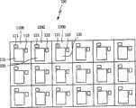
通常,如图1所示,一平板显示器的有机发光二极管(OLED)包括布置成矩阵形式的多个象素100。每个象素100由三个单位像素(unit pixel)组成,即,一个表现红色(R)的单位像素110R,一个表现绿色(G)的单位像素120G,一个表现蓝色(B)的单位像素130B。 Generally, as shown in FIG. 1, an organic light emitting diode (OLED) of a flat panel display includes a plurality of
所述R单位像素110R包括:一个红色电致发光(electroluminescence,EL)装置115,该装置包括一红色(R)发光层;一个用于向所述红色EL装置115供应电流的驱动晶体管113;和一个用于开关从所述驱动晶体管113供应到所述红色EL装置115的电流的开关晶体管111。 The R-
所述G单位像素120G包括:一个绿色EL装置125,该装置包括一绿色(G)发光层;一个用于向所述绿色EL装置125供应电流的驱动晶体管123;和一个用于开关从所述驱动晶体管123供应到所述绿色EL装置125的电流的开关晶体管121。 The G-
所述B单位像素130B包括:一个蓝色EL装置135,该装置包括一蓝色(B)发光层;一个用于向所述蓝色EL装置135供应电流的驱动晶体管133;和一个用于开关从所述驱动晶体管133供应到所述蓝色EL装置135的电流的开关晶体管131。 The B-
常规地,一OLED装置的R、G和B单位像素110R、120G和130B的 所述驱动晶体管113、123和133具有相同尺寸,也就是具有相同的沟道层的宽度W与长度L的比率W/L,并且按照它们发光效率的顺序,所述EL装置的顺序为B、R和G单位像素。在所述常规的OLED中,由于R、G和B单位像素110R、120G和130B的所述驱动晶体管113、123和133的沟道层的尺寸相同,而所述R、G和B的EL装置115、125和135的发光效率彼此不同,所以很难实现白平衡。 Conventionally, the R, G, and
为了实现所述白平衡,对于具有高发光效率的EL装置例如绿色EL装置,应该供应一个相对小量的电流,且对于具有较低发光效率的红色和蓝色EL装置,应该供应一个相对大量的电流。 In order to realize the white balance, a relatively small amount of current should be supplied to EL devices having high luminous efficiency such as green EL devices, and a relatively large amount of current should be supplied to red and blue EL devices having lower luminous efficiencies. current. the
这里,当所述驱动晶体管处于饱和状态时,由于通过所述驱动晶体管流到所述EL装置的电流Id开始流动,所述电流表达如下: Here, when the driving transistor is in a saturated state, since the current Id flowing to the EL device through the driving transistor starts to flow, the current is expressed as follows:
(1)Id=CoxμW(Vg-Vth)2/2L (1)Id=CoxμW(Vg-Vth)2 /2L
因此,为了实现白平衡而控制流到所述EL装置的电流的一种方法是使得R、G和B单位像素的驱动晶体管的尺寸(也就是,所述沟道层的宽度W和长度L的比率W/L)不同,并且因此控制流到所述R、G和B单位像素的EL装置的电流量。根据所述晶体管的尺寸控制流到所述EL装置的电流量的方法公开在日本特开专利公告第2001-109399中。在该日本专利中,根据每个R、G和B单位像素中的EL装置的发光效率,将所述R、G和B单位像素的驱动晶体管的尺寸形成为不相同。也就是,通过使具有高发光效率的表现绿色(G)的单位像素的驱动晶体管的尺寸小于具有相对低发光效率的表现红色(R)或蓝色(B)的单位像素的驱动晶体管的尺寸,来控制流到所述R、G和B单位像素的EL装置的电流量。 Therefore, one way to control the current flow to the EL device for white balance is to make the dimensions of the drive transistors of the R, G, and B unit pixels (that is, the width W and length L of the channel layer The ratio W/L) is different, and thus controls the amount of current flowing to the EL devices of the R, G, and B unit pixels. A method of controlling the amount of current flowing to the EL device according to the size of the transistor is disclosed in Japanese Laid-Open Patent Publication No. 2001-109399. In this Japanese patent, the sizes of the driving transistors of the R, G and B unit pixels are formed differently according to the luminous efficiency of the EL device in each of the R, G and B unit pixels. That is, by making the size of a driving transistor of a unit pixel expressing green (G) having high luminous efficiency smaller than that of a unit pixel expressing red (R) or blue (B) having relatively low luminous efficiency, to control the amount of current flowing to the EL devices of the R, G, and B unit pixels. the
实现所述白平衡的另一种方法是使所述R、G和B单位像素的发光层的大小不同,这公开在日本特开专利公告第2001-290441号上。在该日本专利中,根据所述R、G和B单位像素的EL装置的发光效率,通过使发光面积不同而使从所述R、G和B单位像素上产生相同的发光。也就是,通过使具有低发光效率的R或B单位像素的发光面积大于具有相对高发光效率的G单位像素的发光面积从而在所述R、G和B单位像素上产生相同的发光。 Another method of achieving the white balance is to make the sizes of the light emitting layers of the R, G, and B unit pixels different, which is disclosed in Japanese Laid-Open Patent Publication No. 2001-290441. In this Japanese patent, the same luminescence is generated from the R, G and B unit pixels by making the light emitting areas different according to the luminous efficiencies of the EL devices of the R, G and B unit pixels. That is, the same light emission is generated on the R, G, and B unit pixels by making the light emitting area of the R or B unit pixel having low luminous efficiency larger than that of the G unit pixel having relatively high luminous efficiency. the
但是,在上述实现白平衡的常规方法中,所述R、G和B单位像素中的具有低发光效率的单位像素的发光面积变大,或者增加所述R、G和B单位像素中具有低发光效率的单位像素的晶体管的尺寸。这会造成每个单位像素的充电面积增加的问题,且因此不易将本发明应用在高分辨率的显示中。 However, in the above-mentioned conventional method for achieving white balance, the light-emitting area of the unit pixel with low light-emitting efficiency among the R, G, and B unit pixels becomes large, or the light-emitting area of the unit pixel with low light-emitting efficiency among the R, G, and B unit pixels is increased. Luminous efficiency unit pixel transistor size. This causes a problem that the charging area per unit pixel increases, and thus it is not easy to apply the present invention to a high-resolution display. the
发明内容Contents of the invention
本发明的一个方面在于提供一种平板显示器及其制造方法,其中可以实现白平衡而不增加象素的面积。 An aspect of the present invention is to provide a flat panel display and a method of manufacturing the same, in which white balance can be achieved without increasing the area of pixels. the
本发明的另一个方面在于提供一种平板显示器及其制造方法,其中通过使R、G和B单位像素中驱动晶体管的沟道层具有不同的电流迁移率,可以实现白平衡。 Another aspect of the present invention is to provide a flat panel display and a manufacturing method thereof, wherein white balance can be achieved by making channel layers of driving transistors in R, G, and B unit pixels have different current mobility. the
本发明的又一个方面在于提供一种平板显示器及其制造方法,其中通过使R、G和B单位像素中驱动晶体管的沟道层具有不同方向的结晶化,可以实现白平衡。 Still another aspect of the present invention is to provide a flat panel display and a method of manufacturing the same, wherein white balance can be achieved by crystallizing channel layers of driving transistors in R, G, and B unit pixels in different directions. the
本发明的再一个方面在于提供一种平板显示器及其制造方法,其中可通过使R、G和B单位像素中驱动晶体管的沟道层的电阻值不同来实现白平衡。 Still another aspect of the present invention is to provide a flat panel display and a manufacturing method thereof, wherein white balance can be achieved by making resistance values of channel layers of driving transistors in R, G, and B unit pixels different. the
本发明的还有一个方面在于提供一种平板显示器及其制造方法,其中通过使包括在每个R、G和B单位像素的驱动晶体管的沟道层内的一非结晶硅膜的长度不同,可以实现白平衡。 Still another aspect of the present invention is to provide a flat panel display and a manufacturing method thereof, wherein by making the length of an amorphous silicon film included in the channel layer of the driving transistor of each of R, G, and B unit pixels different, White balance can be achieved. the
根据本发明的一个示例性实施例,提供一种平板显示器,包括多个象素,其中每个象素包括R、G和B单位像素以分别表现红色(R)、绿色(G)和蓝色(B),并且每个单位像素包括至少一个晶体管,其中在R、G和B单位像素中的至少两个单位像素的晶体管包括电流迁移率不同的沟道层,和红色、绿色和蓝色单位像素的晶体管的该沟道层由多晶硅膜制成。 According to an exemplary embodiment of the present invention, there is provided a flat panel display including a plurality of pixels, wherein each pixel includes R, G and B unit pixels to represent red (R), green (G) and blue, respectively (B), and each unit pixel includes at least one transistor, wherein the transistors of at least two unit pixels among R, G, and B unit pixels include channel layers different in current mobility, and red, green, and blue units This channel layer of the transistor of the pixel is made of a polysilicon film. the
在R、G和B单位像素中的至少一个晶体管包括一沟道层,该沟道层在每个象素上具有相同的尺寸。所述R、G和B单位像素分别包括光发射装置。控制供应到每个单位像素的光发射装置的电流的晶体管包括在每个象素上尺寸都相同的沟道层,并且用于驱动具有所述单位像素的光发射装置中最高发光效率的光发射装置的晶体管的电流迁移率小于用于驱动具有相对低发光效率的光发射装置的晶体管的电流迁移率。 At least one transistor in the R, G, and B unit pixels includes a channel layer having the same size in each pixel. The R, G, and B unit pixels include light emitting devices, respectively. The transistor controlling the current supplied to the light-emitting device of each unit pixel includes a channel layer having the same size on each pixel, and is used to drive light emission with the highest luminous efficiency in the light-emitting device having the unit pixel. The current mobility of the transistors of the device is smaller than that of a transistor used to drive a light-emitting device having relatively low luminous efficiency. the
所述R、G和B单位像素的晶体管的沟道层可以由彼此具有不同结晶化方向的多晶硅膜制成。用于驱动具有所述光发射装置中最高发光效率的光 发射装置的晶体管的沟道层可以由金属诱导结晶化(metal inducedcrystallization,MIC)多晶硅膜制成,并且用于驱动具有相对低发光效率的光发射装置的晶体管的沟道层可以由金属诱导横向结晶化(metal inducedlateral crystallization,MILC)多晶硅膜制成。 The channel layers of the transistors of the R, G, and B unit pixels may be made of polysilicon films having crystallization directions different from each other. For driving light with the highest luminous efficiency in the light emitting deviceA channel layer of a transistor of an emission device may be made of a metal-induced crystallization (MIC) polysilicon film, and a channel layer of a transistor for driving a light-emitting device having relatively low luminous efficiency may be made of a metal-induced lateral crystallization It is made of metal induced lateral crystallization (MILC) polysilicon film. the
所述R、G和B单位像素还可分别包括由所述晶体管驱动的光发射装置,并且所述R、G和B单位像素包括一个用于驱动光发射装置的驱动晶体管和用于开启或关断所述驱动晶体管的开关晶体管。 The R, G, and B unit pixels may further include light emitting devices driven by the transistors, respectively, and the R, G, and B unit pixels include a driving transistor for driving the light emitting devices and a driving transistor for turning on or off switch transistor off the drive transistor. the
所述R、G和B单位像素的所述开关晶体管的沟道层可以由MIC多晶硅膜制成。具有所述R、G和B单位像素中最高发光效率的单位像素的驱动晶体管具有一个由MIC多晶硅膜制成的沟道层,并且具有相对低发光效率的单位像素的驱动晶体管具有一个由MILC多晶硅膜制成的沟道层。 Channel layers of the switching transistors of the R, G, and B unit pixels may be made of an MIC polysilicon film. The driving transistor of the unit pixel having the highest luminous efficiency among the R, G, and B unit pixels has a channel layer made of MIC polysilicon film, and the driving transistor of the unit pixel having relatively low luminous efficiency has a channel layer made of MILC polysilicon film. Membrane made of channel layer. the
所述R、G和B单位像素的所述开关晶体管的沟道层可以由MILC多晶硅膜制成,以及具有所述R、G和B单位像素中最高发光效率的驱动晶体管可以具有一个由MIC多晶硅膜制成的沟道层,而具有相对低发光效率的单位像素的驱动晶体管可以具有一个由MILC多晶硅膜制成的沟道层。 The channel layers of the switching transistors of the R, G, and B unit pixels may be made of MILC polysilicon film, and the driving transistors having the highest luminous efficiency among the R, G, and B unit pixels may have a layer made of MIC polysilicon film. film, while the driving transistor of a unit pixel having relatively low luminous efficiency may have a channel layer made of MILC polysilicon film. the
具有所述R、G和B单位像素中最高发光效率的单位像素的开关晶体管和驱动晶体管可以具有由MIC多晶硅膜制成的沟道层,并且具有相对低发光效率的单位像素的驱动晶体管和开关晶体管可具有一个由MILC多晶硅膜制成的沟道层。 The switching transistor and the driving transistor of the unit pixel having the highest luminous efficiency among the R, G, and B unit pixels may have a channel layer made of MIC polysilicon film, and the driving transistor and the switching transistor of the unit pixel having relatively low luminous efficiency The transistor may have a channel layer made of MILC polysilicon film. the
同样,在一个包括多个象素的平板显示器中,其中每个所述象素包括R、G和B单位像素,并且每个所述单位像素包括至少一个晶体管,提供了一种制造该平板显示器的方法,包括在一个绝缘衬底上形成一非结晶化的硅膜和在所述非结晶硅膜上形成一第一和一第二MILC掩模。所述方法还包括:在所述衬底上淀积MILC用金属膜;使所述非结晶硅膜结晶成为一多晶硅膜,以使一个相应于所述第一和第二掩模的部分通过MILC方法结晶并且剩余部分通过MIC方法结晶;移去所述第一和第二掩模和金属膜;并且对所述多晶硅膜构图,而使得具有所述R、G和B单位像素中最高发光效率的一个单位像素的晶体管的半导体层由使用MIC方法结晶化的多晶硅膜制成,且具有相对低发光效率的单位像素的晶体管的半导体层由使用MILC方法结晶化的多晶硅膜制成。 Also, in a flat panel display including a plurality of pixels, wherein each of said pixels includes R, G, and B unit pixels, and each of said unit pixels includes at least one transistor, a method for manufacturing the flat panel display is provided. A method comprising forming an amorphized silicon film on an insulating substrate and forming a first and a second MILC mask on the amorphized silicon film. The method further includes: depositing a metal film for MILC on the substrate; crystallizing the amorphous silicon film into a polysilicon film so that a portion corresponding to the first and second masks passes through the MILC method crystallization and the remaining portion is crystallized by the MIC method; the first and second masks and the metal film are removed; and the polysilicon film is patterned so as to have the highest luminous efficiency among the R, G, and B unit pixels The semiconductor layer of the transistor of one unit pixel is made of a polysilicon film crystallized using the MIC method, and the semiconductor layer of the transistor of a unit pixel having relatively low luminous efficiency is made of a polysilicon film crystallized using the MILC method. the
附图说明Description of drawings
通过对实施例的详细描述并参考附图,使本领域普通技术人员更明白本发明的上述的和其它特征及优点。 The above-mentioned and other features and advantages of the present invention will be more apparent to those skilled in the art by describing the embodiments in detail and referring to the accompanying drawings. the
图1为一常规平板显示器的R、G和B单位像素的分布图; Fig. 1 is the distribution figure of R, G and B unit pixel of a conventional flat panel display;
图2A、2B、2C和2D为制造根据本发明实施例的R、G和B单位像素的驱动晶体管的方法的视图; 2A, 2B, 2C and 2D are views of methods of manufacturing drive transistors of R, G and B unit pixels according to an embodiment of the present invention;
图3示出根据MIC/MILC结晶方法时栅电压和漏电压之间的关系; Figure 3 shows the relationship between gate voltage and drain voltage according to the MIC/MILC crystallization method;
图4A、4B、4C和4D为制造根据本发明另一个实施例的R、G和B单位像素的驱动晶体管的方法的剖面图。 4A, 4B, 4C and 4D are cross-sectional views of a method of manufacturing driving transistors of R, G and B unit pixels according to another embodiment of the present invention. the
具体实施方式Detailed ways
下面将参考表示本发明实施例的附图对本发明进行详细地描述。但是,本发明可以用不同的形式实施并且不应被限制在这里叙述的实施例内。相反,这些被提供的实施例是为了使本公开完全和充分,并且向本领域普通技术人员充分表达本发明的范围。在附图中,为了清楚起见,层的厚度和区域都被放大。在整个说明书中,相同的附图标记表示相同的部件。 Hereinafter, the present invention will be described in detail with reference to the accompanying drawings showing embodiments of the invention. However, the present invention may be embodied in different forms and should not be limited to the embodiments set forth herein. Rather, these embodiments are provided so that this disclosure will be thorough and complete, and will fully convey the scope of the invention to those skilled in the art. In the drawings, the thicknesses of layers and regions are exaggerated for clarity. Throughout the specification, the same reference numerals refer to the same parts. the
图2A、2B、2C和2D为制造根据本发明实施例的R、G和B单位像素的驱动晶体管的方法的视图。图2A、2B、2C和2D的剖面结构表示有机发光二极管中每个象素的所述R、G和B单位像素中的驱动晶体管。 2A, 2B, 2C and 2D are views of a method of manufacturing driving transistors of R, G and B unit pixels according to an embodiment of the present invention. 2A, 2B, 2C and 2D are cross-sectional structures showing driving transistors in the R, G and B unit pixels of each pixel in an organic light emitting diode. the
参考图2A,在一个绝缘衬底200上形成一个图中未显示的缓冲层,并且在所述缓冲层上形成一非结晶化硅膜210。在所述非结晶化硅膜210上形成用于MILC的多个掩模221和225,并且在整个衬底表面上形成一个金属膜230。 Referring to FIG. 2A, an unshown buffer layer is formed on an insulating
所述用于MILC的掩模221和225形成在对应于待形成所述R和B单位像素的区域201和205上。由于用于MILC的掩模没有在待形成G单位像素的区域203上形成,所述金属膜230被形成为与所述非结晶化硅膜210直接接触。虽然在本发明中使用氧化膜作为MILC用掩模221和225,如感光膜的其它膜也可以代替所述氧化膜。 The
参考图2B,通过进行一个结晶化工艺,所述非结晶化硅膜210结晶化成为一多晶硅膜240。这里,通过所述MIC和MILC方法形成所述多晶硅膜240,其中对应于掩模221的多晶硅膜240的部分241经由MILC方法结晶,且对应于掩模225的部分245也用MILC方法结晶。直接与所述金属膜230接触的部分243,也就是包括待形成所述G单位像素的区域203的剩余部分243经由MIC方法完全结晶。 Referring to FIG. 2B, the amorphous silicon film 210 is crystallized into a
参考图2C,在去掉用于MILC的掩模221和225及所述金属膜230后,通过使用一个用于形成所述驱动晶体管的半导体层的掩模(图中未显示)对所述多晶硅膜240构图,以形成所述R、G和B单位像素的驱动晶体管的 半导体层251、253和255。这里,所述单位像素的驱动晶体管的半导体层251、253和255的尺寸全部相同。 Referring to FIG. 2C, after removing the
在所述R、G和B单位像素中,R单位像素的驱动晶体管的半导体层251由通过MILC方法结晶化的所述多晶硅膜241构成。G单位像素的驱动晶体管的半导体层253由通过MIC方法结晶化的所述多晶硅膜243构成。B单位像素的驱动晶体管的半导体层255由通过MILC方法结晶化的所述多晶硅膜245构成。 In the R, G, and B unit pixels, the
参考图2D,在所述衬底上包括所述半导体层251、253和255上形成一栅绝缘膜260,在所述栅绝缘膜260上形成每个单位像素的驱动晶体管的栅极271、273和275。分别使用栅极271、273和275作为掩模,通过执行将所希望导电类型的杂质掺入到所述半导体层251、253和255的离子注入,形成每个驱动晶体管的源/漏区281、283和285。 Referring to FIG. 2D, a
尽管在附图中未显示,在整个衬底表面上可以形成一个层间绝缘膜。可以通过刻蚀所述层间绝缘膜和栅绝缘层260形成用于露出所述源/漏区281、283和285的接触孔,并且可以形成穿过所述接触孔与所述源/漏区281、283和285电连接的源/漏区,因此制造出所述驱动晶体管。 Although not shown in the drawings, an interlayer insulating film may be formed on the entire surface of the substrate. Contact holes for exposing the source/
在使用上述方法制造的本发明的平板显示器中,所述R、G和B单位像素的所述驱动晶体管可以包括具有同样长度Lrc、Lgc和Lbc的沟道层。所述R和B单位像素的驱动晶体管可以分别包括由以MILC方法结晶的多晶硅膜241和245制成的沟道层,并且所述G单位像素的驱动晶体管可以包括由以MIC方法结晶的多晶硅膜243制成的沟道层。因此,所述R、G和B单位像素的驱动晶体管可以具有相同尺寸的沟道层。而且,所述沟道层的电流迁移率可以根据所述R、G和B单位像素的驱动晶体管的所述沟道层的结晶化方向而改变。 In the flat panel display of the present invention manufactured using the above method, the driving transistors of the R, G, and B unit pixels may include channel layers having the same lengths Lrc, Lgc, and Lbc. The driving transistors of the R and B unit pixels may include channel layers made of
具有低发光效率的所述R和B单位像素的驱动晶体管的所述沟道层可以由具有高电流迁移率的、以MILC方法结晶的多晶硅膜241和245制成,而具有较高发光效率的所述G单位像素的驱动晶体管的所述沟道层可以由具有低电流迁移率的、以MIC方法结晶的多晶硅膜243制成。 The channel layers of the drive transistors of the R and B unit pixels having low luminous efficiency may be made of
因此,根据本发明的实施例,通过根据所述R、G和B单位像素的EL装置的发光效率改变所述沟道层的结晶化方向,可以确定所述沟道层的电阻值,具有相对低发光效率的所述R和B单位像素的驱动晶体管的所述沟道 层由按照MILC方法结晶的多晶硅膜制成,其具有与沟道长度同一方向上的结晶化方向,也就是水平方向,并且因此具有相当低的电阻值。同样,具有相对高发光效率的所述G单位像素的驱动晶体管的所述沟道层由按照MIC方法结晶的多晶硅膜制成,其具有垂直于沟道长度方向的结晶化方向,也就是垂直方向,并且因此具有相当高的电阻值。 Therefore, according to an embodiment of the present invention, by changing the crystallization direction of the channel layer according to the luminous efficiencies of the EL devices of the R, G, and B unit pixels, the resistance value of the channel layer can be determined, with a relative The channels of the driving transistors of the R and B unit pixels with low luminous efficiencyThe layer is made of a polysilicon film crystallized according to the MILC method, which has a crystallization direction in the same direction as the channel length, that is, a horizontal direction, and thus has a relatively low resistance value. Also, the channel layer of the drive transistor of the G unit pixel having relatively high luminous efficiency is made of a polysilicon film crystallized according to the MIC method, which has a crystallization direction perpendicular to the channel length direction, that is, the vertical direction , and thus have a rather high resistance value. the
因此,通过使所述R、G和B单位像素的沟道层的尺寸相同并且使它们的结晶化方向不同,并且因此使电流迁移率彼此不相同,可以实现本发明的白平衡。 Therefore, the white balance of the present invention can be achieved by making the channel layers of the R, G, and B unit pixels the same size and making their crystallization directions different, and thus making current mobility different from each other. the
图3为包括通过MIC和MILC方法结晶的半导体层的薄膜晶体管的栅电压和漏电压之间关系的视图。图3表示即使在所述薄膜晶体管具有相同的尺寸(W/L)和沟道方向的情况下,根据所述沟道层的多晶硅膜的微细结构,电流量也可以不同。 FIG. 3 is a view showing a relationship between a gate voltage and a drain voltage of a thin film transistor including a semiconductor layer crystallized by MIC and MILC methods. FIG. 3 shows that even when the thin film transistors have the same size (W/L) and channel direction, the amount of current may differ depending on the fine structure of the polysilicon film of the channel layer. the
参考图3,应该注意到:MILC多晶硅薄膜晶体管中所述漏极电流相对于栅电压的特征曲线优于MIC多晶硅薄膜晶体管中所述漏极电流相对于栅电压的特征曲线。因此所述由以MILC方法结晶的多晶硅膜制成的薄膜晶体管的电流迁移率高于由以MIC方法结晶的多晶硅膜制成的薄膜晶体管的电流迁移率。 Referring to FIG. 3, it should be noted that the characteristic curve of the drain current versus the gate voltage in the MILC polysilicon thin film transistor is better than the characteristic curve of the drain current versus the gate voltage in the MIC polysilicon thin film transistor. Therefore, the current mobility of the thin film transistor made of the polysilicon film crystallized by the MILC method is higher than that of the thin film transistor made of the polysilicon film crystallized by the MIC method. the
因此,在本发明的一个实施例中,具有相对较高发光效率的所述绿色单位像素的驱动晶体管的沟道层由MIC多晶硅膜制成,并且具有相对较低发光效率的所述红色和蓝色单位像素的驱动晶体管的沟道层由MILC多晶硅膜制成。通过使流过所述红色或蓝色单位像素的驱动晶体管的电流高于流过所述绿色单位像素的驱动晶体管的电流可以实现白平衡。 Therefore, in one embodiment of the present invention, the channel layer of the drive transistor of the green unit pixel with relatively high luminous efficiency is made of MIC polysilicon film, and the red and blue unit pixels with relatively low luminous efficiency The channel layer of the drive transistor of the color unit pixel is made of MILC polysilicon film. White balance may be achieved by making the current flowing through the driving transistor of the red or blue unit pixel higher than the current flowing through the driving transistor of the green unit pixel. the
在本发明的一个实施例中,即使根据所述R、G和B的EL装置的发光效率使驱动晶体管的沟道层由通过MIC和/或MILC方法结晶的多晶硅膜形成,所述MIC和/或MILC方法也可以应用于所述R、G和B单位像素的开关晶体管。例如,所有所述R、G和B单位像素的开关晶体管的沟道层可以由通过所述MIC方法和/或MILC方法结晶的多晶硅膜构成。或者,具有较高发光效率的所述G单位像素的开关晶体管可以具有由通过所述MIC方法结晶的多晶硅膜构成的沟道层,而具有较低发光效率的所述R或B单位像素的开关晶体管可以具有由用MILC方法结晶的多晶硅膜构成的沟道层。所述R、G和B单位像素的所述驱动晶体管和所述开关晶体管的半导体层 可以具有与沟道方向相同或不同的结晶化方向。 In one embodiment of the present invention, even if the channel layer of the driving transistor is formed of a polysilicon film crystallized by the MIC and/or MILC method according to the luminous efficiencies of the EL devices of the R, G, and B, the MIC and/or Or the MILC method can also be applied to the switch transistors of the R, G and B unit pixels. For example, the channel layers of the switching transistors of all the R, G, and B unit pixels may be composed of a polysilicon film crystallized by the MIC method and/or the MILC method. Alternatively, the switching transistor of the G unit pixel having higher luminous efficiency may have a channel layer composed of a polysilicon film crystallized by the MIC method, while the switching transistor of the R or B unit pixel having lower luminous efficiency The transistor may have a channel layer composed of a polysilicon film crystallized by the MILC method. The driving transistor of the R, G and B unit pixels and the semiconductor layer of the switching transistorIt may have the same or different crystallization direction as the channel direction. the
即使本发明的一个实施例的所述沟道层被描述为通过所述MIC/MILC方法结晶,但所述R、G和B单位像素的驱动晶体管的沟道层可以具有彼此不同的结晶方法,以使本发明中可以使用彼此具有不同电流迁移率的所有结晶化方法。 Even though the channel layer of one embodiment of the present invention is described as being crystallized by the MIC/MILC method, the channel layers of the driving transistors of the R, G, and B unit pixels may have different crystallization methods from each other, So that all crystallization methods having different current mobility from each other can be used in the present invention. the
图4A、4B、4C和4D为根据本发明另一个实施例的制造R、G和B单位像素的驱动晶体管的方法的工序剖视图。图4A、4B、4C和4D的剖视结构表示在有机发光二极管中每个象素的所述R、G和B单位像素的驱动晶体管。 4A, 4B, 4C and 4D are process cross-sectional views of a method of manufacturing driving transistors for R, G and B unit pixels according to another embodiment of the present invention. 4A, 4B, 4C and 4D are cross-sectional structures showing driving transistors of the R, G and B unit pixels of each pixel in an organic light emitting diode. the
参考图4A,尽管在附图中未显示,在一个绝缘衬底400上形成一个缓冲层,并且在所述衬底上形成一个非结晶硅层410。在所述非结晶化硅层410上形成多个用于MILC的掩模421、423和425及在整个衬底表面上形成一个金属层430。 Referring to FIG. 4A, although not shown in the drawing, a buffer layer is formed on an insulating
将所述用于MILC的掩模421、423和425形成为彼此具有不同的宽度,其中所述掩模宽度从高到低的顺序为第二掩模423、第一掩模421和第三掩模425。所述第一掩模421被形成在相应地要形成所述R、G和B单位像素中的R单位像素的驱动晶体管(图1中的113)的区域,所述第二掩模423被形成在要形成所述G单位像素的驱动晶体管(图1中的123)的区域。所述第三掩模425被形成在要形成所述B单位像素的驱动晶体管(图1中的133)的区域。 The masks 421, 423, and 425 for MILC are formed to have different widths from each other, wherein the order of the mask widths from high to low is the second mask 423, the first mask 421, and the third mask. Modulo 425. The first mask 421 is formed in a region where the driving transistor (113 in FIG. 1 ) of the R unit pixel among the R, G, and B unit pixels is to be formed correspondingly, and the second mask 423 is formed In the area where the driving transistor ( 123 in FIG. 1 ) of the G unit pixel is to be formed. The third mask 425 is formed in a region where the driving transistor ( 133 in FIG. 1 ) of the B-unit pixel is to be formed. the
参考图4B,执行结晶化工艺,以将所述非结晶硅膜410结晶为多晶硅膜440,其中相应于所述非结晶硅膜410中的掩模421、423和425的部分通过MILC方法结晶化成为多晶硅膜441、443和445。在所述掩模421、423和425之间的、直接与所述金属层430接触的部分使用MIC方法结晶化形成多晶硅膜447。 Referring to FIG. 4B, a crystallization process is performed to crystallize the amorphous silicon film 410 into a polysilicon film 440, wherein portions corresponding to the masks 421, 423, and 425 in the amorphous silicon film 410 are crystallized by the MILC method. These become
由于用于MILC的所述第一到第三掩模421、423和425彼此具有不同的宽度,对应于具有一相对较窄宽度的所述第三掩模425的多晶硅膜440的部分由MILC方法结晶化,并且对应于具有一相对较宽宽度的所述第一和第二掩模421和423的部分分别由MILC方法部分地结晶,留下未改变的所述非结晶硅膜411和413。 Since the first to third masks 421, 423, and 425 for MILC have different widths from each other, the portion of the polysilicon film 440 corresponding to the third mask 425 having a relatively narrow width is processed by the MILC method. crystallized, and portions corresponding to the first and second masks 421 and 423 having a relatively wide width are partially crystallized by the MILC method, respectively, leaving the
也就是,在对应于所述第一掩模421的多晶硅膜440之中,所述非结晶 硅膜411存在于以MILC方法结晶的部分441之间。而且,在对应于所述第二掩模的多晶硅膜440之中,所述非结晶硅膜413存在于以MILC方法结晶化的部分443之间。由于所述第一掩模421的宽度相对小于所述第二掩模423的宽度,对应于所述第二掩模423的所述非结晶硅膜413的长度大于对应于所述第一掩模421的所述非结晶硅膜411的长度。 That is, in the polysilicon film 440 corresponding to the first mask 421, the amorphousThe
参考图4C,在去掉用于MILC方法的掩模421、423和425及所述金属层430后,通过使用形成半导体层用的掩模(图中未显示)对所述多晶硅膜440构图,形成用于所述R、G和B单位像素的驱动晶体管的半导体层451、453和455。在所述多晶硅膜440中通过所述MILC方法结晶化的部分441及存在于所述部分441之间的所述非结晶硅膜411形成了用于所述R、G和B单位像素中的所述R单位像素的驱动晶体管的所述半导体层451。在所述多晶硅膜440中通过所述MILC方法结晶化的部分443及存在于所述部分443之间的所述非结晶硅膜413形成了用于所述G单位像素的驱动晶体管的所述半导体层453。另一方面,在所述多晶硅膜中仅通过所述MILC方法结晶化的所述多晶硅膜445形成了用于所述B单位像素的驱动晶体管的所述半导体层455。 Referring to FIG. 4C, after removing the masks 421, 423 and 425 and the metal layer 430 for the MILC method, the polysilicon film 440 is patterned by using a mask (not shown) for forming a semiconductor layer to form Semiconductor layers 451, 453, and 455 for driving transistors of the R, G, and B unit pixels. The
参考图4D,在整个所述衬底包括所述半导体层451、453和455的表面上淀积一个栅绝缘膜460。在所述膜460上淀积一导电材料如一金属膜,并且然后使用用于形成所述栅极的掩模(图中未显示)对所述导电材料构图,形成每个所述R、G和B单位像素的驱动晶体管的栅极471、473和475。然后,使用所述栅极471、473和475作为掩模将所期望导电类型的高浓度杂质离子注入到所述半导体层451、453和455内,形成所述驱动晶体管的源/漏区481、483和485。 Referring to FIG. 4D, a
即使在附图中未显示出,所述驱动晶体管可以通过下述步骤制造:在整个所述衬底表面上形成一个层间绝缘膜,通过刻蚀所述层间绝缘膜和所述栅绝缘膜460形成露出所述源/漏区481、483和485的接触孔,并且形成穿过所述接触孔与所述源/漏区481、483和485电连接的源/漏电极。 Even though not shown in the drawings, the driving transistor can be manufactured by forming an interlayer insulating film on the entire surface of the substrate, by etching the interlayer insulating film and the
在通过上述方法制造的根据本发明的平板显示器中,所述R单位像素的驱动晶体管的沟道层482可以由用MILC方法结晶化的多晶硅膜441和非结晶硅膜411制成。沟道层的长度Lrc为所述多晶硅膜441的长度Lr1和Lr2及所述非结晶硅膜411的长度Lra的总和,也就是,Lrc=Lr1+Lra+Lr2。 所述G单位像素的驱动晶体管的沟道层484由用MILC方法结晶化的多晶硅膜443和非结晶硅膜413制成。沟道层总长度Lgc为所述多晶硅膜443的长度Lg1和Lg2及所述非结晶硅膜413的长度Lga的总和,也就是,Lgc=Lg1+Lga+Lg2。所述B单位像素的驱动晶体管的沟道层486由仅用MILC方法结晶化的多晶硅膜445制成,沟道层总长度Lbc等于所述多晶硅膜445的长度Lb。 In the flat panel display according to the present invention manufactured by the above method, the
在所述R、G和B单位像素的驱动晶体管中,由于沟道层482、484和486的长度相同,为Lrc=Lgc=Lbc,所述驱动晶体管的沟道层的电阻值根据包括在每个沟道层中的所述非结晶硅膜的长度而变化。而本发明的实施例可以构造成根据所述R、G和B单位像素的EL装置的发光效率来决定所述沟道层的电阻值,因为具有相对最低发光效率的所述B单位像素的沟道层486由以MILC方法结晶化的多晶硅膜制成,其沟道层的电阻值相对较低。 In the driving transistors of the R, G and B unit pixels, since the lengths of the channel layers 482, 484 and 486 are the same, which is Lrc=Lgc=Lbc, the resistance value of the channel layer of the driving transistor is included in each The length of the amorphous silicon film in each channel layer varies. However, the embodiments of the present invention can be configured to determine the resistance value of the channel layer according to the luminous efficiencies of the EL devices of the R, G, and B unit pixels, because the channel of the B unit pixel with the relatively lowest luminous efficiency The
同样,具有相对较高发光效率的所述R或G单位像素的沟道层482或484包括在所述多晶硅膜之间的一个非结晶硅膜,使所述沟道层的电阻值相对增加。由于所述R单位像素的EL装置具有比所述G单位像素的EL装置更低的发光效率,在所述R单位像素的沟道层482中存在的所述非结晶硅膜411的长度Lra被形成为相对短于在所述G单位像素的沟道层484中存在的所述非结晶硅膜413的长度Lga。 Also, the
因此,当根据本发明另一个实施例中的所述R、G和B单位像素的驱动晶体管的沟道层的长度被形成为相等时,在所述R、G和B单位像素的驱动晶体管的沟道层中存在的所述非结晶硅膜被形成为彼此具有不同的长度。因此,通过使所述驱动晶体管的沟道层的电阻值彼此不同而能够实现白平衡。 Therefore, when the lengths of the channel layers of the driving transistors of the R, G and B unit pixels according to another embodiment of the present invention are formed to be equal, the driving transistors of the R, G and B unit pixels The amorphous silicon films present in the channel layer are formed to have different lengths from each other. Therefore, white balance can be achieved by making the resistance values of the channel layers of the driving transistors different from each other. the
根据本发明的另一个实施例,通过进行结晶化处理以使通过所述MILC处理在所述沟道层中存在所述非结晶硅膜,从而改变所述R、G和B单位像素的驱动晶体管的所述沟道层的电阻值。但是,通过使用其它的结晶化处理代替所述MILC工艺,使所述沟道层包括彼此长度不同的非结晶硅膜,来改变所述R、G和B单位像素的驱动晶体管的电阻值,该方法也可以用在本发明中。尽管在所述B单位像素的驱动晶体管的沟道层中可能不存在非结晶硅膜,但本发明不限于上述的结构。而是,本发明甚至可以形成为一种结构,其中包括具有一电阻值的非结晶硅膜,该电阻值处于能够使所述R或G 单位像素的沟道层实现白平衡的水平。 According to another embodiment of the present invention, the driving transistors of the R, G and B unit pixels are changed by performing crystallization treatment so that the amorphous silicon film exists in the channel layer by the MILC treatment. The resistance value of the channel layer. However, by changing the resistance values of the drive transistors of the R, G, and B unit pixels by making the channel layer include amorphous silicon films having different lengths from each other by using other crystallization processing instead of the MILC process, the Methods can also be used in the present invention. Although the amorphous silicon film may not exist in the channel layer of the driving transistor of the B-unit pixel, the present invention is not limited to the above-mentioned structure. Rather, the present invention may even be formed as a structure including an amorphous silicon film having a resistance value at which the R or GThe channel layer of the unit pixel realizes the level of white balance. the
根据本发明的另一个实施例,在进行MILC结晶化时通过控制结晶化温度或结晶化时间,可以进行一结晶化处理使得在每个沟道层中存在一非结晶硅膜。可以用所述MILC多晶硅膜形成所述单位像素的开关晶体管的全部沟道区。所述R和G单位像素的驱动晶体管具有在所述多晶硅膜之间的一非结晶硅膜,且所述B单位像素的驱动晶体管可以具有一由多晶硅膜制成的沟道区。 According to another embodiment of the present invention, by controlling the crystallization temperature or crystallization time during MILC crystallization, a crystallization process can be performed so that an amorphous silicon film exists in each channel layer. All channel regions of switching transistors of the unit pixel may be formed with the MILC polysilicon film. The driving transistors of the R and G unit pixels have an amorphous silicon film between the polysilicon films, and the driving transistor of the B unit pixel may have a channel region made of polysilicon film. the
在本发明的上述描述中,没有通过增加所述象素面积实现所述白平衡,而是通过改变所述R、G和B单位像素的沟道层的电流迁移率或电阻值来实现所述白平衡。 In the above description of the present invention, the white balance is not achieved by increasing the pixel area, but by changing the current mobility or resistance value of the channel layer of the R, G and B unit pixels. white balance. the
同样,通过使用MIC/MILC结晶化方法将非结晶硅膜结晶化成为所述多晶硅膜,并且于是形成具有不同电流迁移率的所述R、G和B单位像素的驱动晶体管的半导体层,本发明可以减低工艺成本并且简化工艺。 Also, by crystallizing an amorphous silicon film into the polysilicon film using the MIC/MILC crystallization method, and thus forming the semiconductor layers of the driving transistors of the R, G, and B unit pixels having different current mobility, the present invention The process cost can be reduced and the process can be simplified. the
虽然为了说明的目的对本发明的优选实施例进行了公开,本领域普通技术人员应该明白,在不背离在所附权利要求中公开的本发明的范围和精神的条件下可以作出各种修改、添加和替代。 Although the preferred embodiments of the present invention have been disclosed for illustrative purposes, those of ordinary skill in the art will appreciate that various modifications, additions and and substitute. the
Claims (11)
Applications Claiming Priority (6)
| Application Number | Priority Date | Filing Date | Title |
|---|---|---|---|
| KR24503/2003 | 2003-04-17 | ||
| KR24503/03 | 2003-04-17 | ||
| KR24429/2003 | 2003-04-17 | ||
| KR24429/03 | 2003-04-17 | ||
| KR10-2003-0024429AKR100496422B1 (en) | 2003-04-17 | 2003-04-17 | Flat Panel Display with improved white balance using MILC |
| KR10-2003-0024503AKR100496423B1 (en) | 2003-04-17 | 2003-04-17 | Flat Panel Display with improved white balance |
Related Child Applications (1)
| Application Number | Title | Priority Date | Filing Date |
|---|---|---|---|
| CN2008101102469ADivisionCN101308866B (en) | 2003-04-17 | 2004-04-13 | Flat panel display with improved white balance and method of manufacturing the same |
Publications (2)
| Publication Number | Publication Date |
|---|---|
| CN1541038A CN1541038A (en) | 2004-10-27 |
| CN1541038Btrue CN1541038B (en) | 2012-07-25 |
Family
ID=33161627
Family Applications (1)
| Application Number | Title | Priority Date | Filing Date |
|---|---|---|---|
| CN2004100328879AExpired - LifetimeCN1541038B (en) | 2003-04-17 | 2004-04-13 | Flat panel display with improved white balance |
Country Status (2)
| Country | Link |
|---|---|
| US (2) | US7161180B2 (en) |
| CN (1) | CN1541038B (en) |
Families Citing this family (4)
| Publication number | Priority date | Publication date | Assignee | Title |
|---|---|---|---|---|
| JP4511218B2 (en)* | 2004-03-03 | 2010-07-28 | ルネサスエレクトロニクス株式会社 | Display panel driving method, driver, and display panel driving program |
| KR20060121514A (en)* | 2005-05-24 | 2006-11-29 | 삼성전자주식회사 | Organic light emitting display and manufacturing method |
| KR20160062331A (en)* | 2014-11-24 | 2016-06-02 | 삼성디스플레이 주식회사 | Thin film deposition mask assembly and in-line type thin film deposition apparatus comprising the same |
| CN112259533B (en)* | 2020-10-23 | 2022-07-05 | 福州大学 | White balance implementation method based on quantum dot color conversion |
Citations (4)
| Publication number | Priority date | Publication date | Assignee | Title |
|---|---|---|---|---|
| CN1109212A (en)* | 1993-08-27 | 1995-09-27 | 株式会社半导体能源研究所 | Semiconductor device and manufacturing method thereof |
| US5614733A (en)* | 1993-03-12 | 1997-03-25 | Semiconductor Energy Laboratory Co., Inc. | Semiconductor device having crystalline thin film transistors |
| US6278130B1 (en)* | 1998-05-08 | 2001-08-21 | Seung-Ki Joo | Liquid crystal display and fabricating method thereof |
| US20010045565A1 (en)* | 2000-05-05 | 2001-11-29 | Shunpei Yamazaki | Light emitting device |
Family Cites Families (8)
| Publication number | Priority date | Publication date | Assignee | Title |
|---|---|---|---|---|
| US6366025B1 (en)* | 1999-02-26 | 2002-04-02 | Sanyo Electric Co., Ltd. | Electroluminescence display apparatus |
| JP3670923B2 (en) | 1999-02-26 | 2005-07-13 | 三洋電機株式会社 | Color organic EL display device |
| JP2001109399A (en) | 1999-10-04 | 2001-04-20 | Sanyo Electric Co Ltd | Color display |
| JP2001318627A (en)* | 2000-02-29 | 2001-11-16 | Semiconductor Energy Lab Co Ltd | Light emitting device |
| US6838819B2 (en)* | 2000-06-19 | 2005-01-04 | Lg Electronics Inc. | Full color organic EL display panel, manufacturing method thereof and driving circuit thereof |
| JP5082172B2 (en)* | 2001-02-05 | 2012-11-28 | ソニー株式会社 | Manufacturing method of display device |
| US6891328B2 (en)* | 2001-02-22 | 2005-05-10 | Matsushita Electric Industrial Co., Ltd. | Light source for image reading apparatus and image reading apparatus |
| US6867549B2 (en)* | 2002-12-10 | 2005-03-15 | Eastman Kodak Company | Color OLED display having repeated patterns of colored light emitting elements |
- 2004
- 2004-04-13CNCN2004100328879Apatent/CN1541038B/ennot_activeExpired - Lifetime
- 2004-04-14USUS10/823,712patent/US7161180B2/ennot_activeExpired - Lifetime
- 2006
- 2006-12-14USUS11/610,789patent/US7442594B2/ennot_activeExpired - Lifetime
Patent Citations (4)
| Publication number | Priority date | Publication date | Assignee | Title |
|---|---|---|---|---|
| US5614733A (en)* | 1993-03-12 | 1997-03-25 | Semiconductor Energy Laboratory Co., Inc. | Semiconductor device having crystalline thin film transistors |
| CN1109212A (en)* | 1993-08-27 | 1995-09-27 | 株式会社半导体能源研究所 | Semiconductor device and manufacturing method thereof |
| US6278130B1 (en)* | 1998-05-08 | 2001-08-21 | Seung-Ki Joo | Liquid crystal display and fabricating method thereof |
| US20010045565A1 (en)* | 2000-05-05 | 2001-11-29 | Shunpei Yamazaki | Light emitting device |
Non-Patent Citations (1)
| Title |
|---|
| 全文. |
Also Published As
| Publication number | Publication date |
|---|---|
| US20040207584A1 (en) | 2004-10-21 |
| US7442594B2 (en) | 2008-10-28 |
| US20070085094A1 (en) | 2007-04-19 |
| CN1541038A (en) | 2004-10-27 |
| US7161180B2 (en) | 2007-01-09 |
Similar Documents
| Publication | Publication Date | Title |
|---|---|---|
| US7785942B2 (en) | Active matrix organic EL display device and manufacturing method thereof | |
| TWI590438B (en) | Organic light emitting display panel and method of manufacturing same | |
| CN100420029C (en) | Active matrix organic light emitting diode device and manufacturing method thereof | |
| CN100552977C (en) | Thin film transistor, flat panel display device and manufacturing method thereof | |
| CN100419816C (en) | Flat panel display with thin film transistors | |
| JP2007189218A (en) | Transistor, method of manufacturing the transistor, and organic light emitting display to which the transistor is applied | |
| US7285902B2 (en) | Flat panel display with improved white balance | |
| JP4109265B2 (en) | Organic electroluminescent device and manufacturing method thereof | |
| US7265737B2 (en) | Flat panel display with thin film transistor (TFT) | |
| JP3748827B2 (en) | Organic EL display device manufacturing method | |
| US7442594B2 (en) | Method for manufacturing a flat panel display with improved white balance | |
| US7173368B2 (en) | Flat panel display with thin film transistor (TFT) | |
| JP2004327979A (en) | Thin film transistor and display device using the same | |
| CN100409275C (en) | Flat panel display with thin film transistors | |
| CN101308866B (en) | Flat panel display with improved white balance and method of manufacturing the same | |
| CN1541037B (en) | White balance improved flat panel disply | |
| KR100496422B1 (en) | Flat Panel Display with improved white balance using MILC | |
| CN100576549C (en) | flat panel display device | |
| KR100542985B1 (en) | Flat Panel Display with Improved White Balance | |
| KR100635580B1 (en) | Thin film transistor, flat panel display and manufacturing method | |
| KR100553744B1 (en) | Flat panel display with thin film transistor | |
| KR100496424B1 (en) | Flat Panel Display with improved white balance | |
| KR100600851B1 (en) | Flat Panel Display with Improved White Balance | |
| KR20040094058A (en) | Flat panel display with TFT | |
| JP2017045806A (en) | Thin film transistor, TFT array substrate, display device, and manufacturing method thereof |
Legal Events
| Date | Code | Title | Description |
|---|---|---|---|
| C06 | Publication | ||
| PB01 | Publication | ||
| C10 | Entry into substantive examination | ||
| SE01 | Entry into force of request for substantive examination | ||
| C41 | Transfer of patent application or patent right or utility model | ||
| TA01 | Transfer of patent application right | Effective date of registration:20090109 Address after:Gyeonggi Do, South Korea Applicant after:Samsung Mobile Display Co.,Ltd. Address before:Gyeonggi Do, South Korea Applicant before:Samsung SDI Co.,Ltd. | |
| ASS | Succession or assignment of patent right | Owner name:SAMSUNG MOBILE DISPLAY CO., LTD. Free format text:FORMER OWNER: SAMSUNG SDI CO., LTD. Effective date:20090109 | |
| C14 | Grant of patent or utility model | ||
| GR01 | Patent grant | ||
| ASS | Succession or assignment of patent right | Owner name:SAMSUNG DISPLAY CO., LTD. Free format text:FORMER OWNER: SAMSUNG MOBILE DISPLAY CO., LTD. Effective date:20121017 | |
| C41 | Transfer of patent application or patent right or utility model | ||
| TR01 | Transfer of patent right | Effective date of registration:20121017 Address after:Gyeonggi Do, South Korea Patentee after:SAMSUNG DISPLAY Co.,Ltd. Address before:Gyeonggi Do, South Korea Patentee before:Samsung Mobile Display Co.,Ltd. | |
| CX01 | Expiry of patent term | Granted publication date:20120725 | |
| CX01 | Expiry of patent term |