CN1530725A - Novel conducting element for thin-film transistors used in flat-panel displays - Google Patents
Novel conducting element for thin-film transistors used in flat-panel displaysDownload PDFInfo
- Publication number
- CN1530725A CN1530725ACNA2004100287328ACN200410028732ACN1530725ACN 1530725 ACN1530725 ACN 1530725ACN A2004100287328 ACNA2004100287328 ACN A2004100287328ACN 200410028732 ACN200410028732 ACN 200410028732ACN 1530725 ACN1530725 ACN 1530725A
- Authority
- CN
- China
- Prior art keywords
- layer
- tft
- thin film
- film transistor
- aluminium alloy
- Prior art date
- Legal status (The legal status is an assumption and is not a legal conclusion. Google has not performed a legal analysis and makes no representation as to the accuracy of the status listed.)
- Granted
Links
- 239000010409thin filmSubstances0.000titleclaimsabstractdescription25
- 239000004065semiconductorSubstances0.000claimsabstractdescription44
- XAGFODPZIPBFFR-UHFFFAOYSA-NaluminiumChemical compound[Al]XAGFODPZIPBFFR-UHFFFAOYSA-N0.000claimsabstractdescription41
- 229910052782aluminiumInorganic materials0.000claimsabstractdescription41
- 239000010936titaniumSubstances0.000claimsabstractdescription35
- 229910000838Al alloyInorganic materials0.000claimsabstractdescription32
- RTAQQCXQSZGOHL-UHFFFAOYSA-NTitaniumChemical compound[Ti]RTAQQCXQSZGOHL-UHFFFAOYSA-N0.000claimsabstractdescription21
- 229910052719titaniumInorganic materials0.000claimsabstractdescription21
- NRTOMJZYCJJWKI-UHFFFAOYSA-NTitanium nitrideChemical compound[Ti]#NNRTOMJZYCJJWKI-UHFFFAOYSA-N0.000claimsdescription25
- 238000009792diffusion processMethods0.000claimsdescription23
- 239000000758substrateSubstances0.000claimsdescription17
- PXHVJJICTQNCMI-UHFFFAOYSA-NNickelChemical compound[Ni]PXHVJJICTQNCMI-UHFFFAOYSA-N0.000claimsdescription11
- BASFCYQUMIYNBI-UHFFFAOYSA-NplatinumChemical compound[Pt]BASFCYQUMIYNBI-UHFFFAOYSA-N0.000claimsdescription11
- IJGRMHOSHXDMSA-UHFFFAOYSA-NAtomic nitrogenChemical compoundN#NIJGRMHOSHXDMSA-UHFFFAOYSA-N0.000claimsdescription9
- XUIMIQQOPSSXEZ-UHFFFAOYSA-NSiliconChemical compound[Si]XUIMIQQOPSSXEZ-UHFFFAOYSA-N0.000claimsdescription6
- 239000010949copperSubstances0.000claimsdescription6
- 229910052757nitrogenInorganic materials0.000claimsdescription6
- 229910052710siliconInorganic materials0.000claimsdescription6
- 239000010703siliconSubstances0.000claimsdescription6
- RYGMFSIKBFXOCR-UHFFFAOYSA-NCopperChemical compound[Cu]RYGMFSIKBFXOCR-UHFFFAOYSA-N0.000claimsdescription5
- 229910052779NeodymiumInorganic materials0.000claimsdescription5
- 229910052802copperInorganic materials0.000claimsdescription5
- QEFYFXOXNSNQGX-UHFFFAOYSA-Nneodymium atomChemical compound[Nd]QEFYFXOXNSNQGX-UHFFFAOYSA-N0.000claimsdescription5
- 229910052759nickelInorganic materials0.000claimsdescription5
- 229910052697platinumInorganic materials0.000claimsdescription5
- 239000004411aluminiumSubstances0.000claims3
- ATJFFYVFTNAWJD-UHFFFAOYSA-NTinChemical compound[Sn]ATJFFYVFTNAWJD-UHFFFAOYSA-N0.000claims1
- 238000007669thermal treatmentMethods0.000claims1
- 238000010438heat treatmentMethods0.000abstractdescription28
- 230000015572biosynthetic processEffects0.000abstractdescription14
- 238000000034methodMethods0.000abstractdescription7
- 230000008569processEffects0.000abstractdescription6
- 230000007547defectEffects0.000abstractdescription5
- 239000004973liquid crystal related substanceSubstances0.000description15
- 239000000463materialSubstances0.000description10
- 230000004888barrier functionEffects0.000description9
- 239000000470constituentSubstances0.000description8
- 229910010038TiAlInorganic materials0.000description6
- 239000003990capacitorSubstances0.000description6
- 229910010272inorganic materialInorganic materials0.000description6
- 239000011147inorganic materialSubstances0.000description6
- 229910052751metalInorganic materials0.000description6
- 239000002184metalSubstances0.000description6
- 238000004519manufacturing processMethods0.000description5
- XKRFYHLGVUSROY-UHFFFAOYSA-NArgonChemical compound[Ar]XKRFYHLGVUSROY-UHFFFAOYSA-N0.000description4
- 229910010039TiAl3Inorganic materials0.000description4
- 238000003860storageMethods0.000description4
- 229910045601alloyInorganic materials0.000description3
- 239000000956alloySubstances0.000description3
- 238000000137annealingMethods0.000description3
- 230000008901benefitEffects0.000description3
- 230000002950deficientEffects0.000description3
- 238000005401electroluminescenceMethods0.000description3
- 150000002739metalsChemical class0.000description3
- 229910052786argonInorganic materials0.000description2
- 239000011651chromiumSubstances0.000description2
- 238000009826distributionMethods0.000description2
- 238000001312dry etchingMethods0.000description2
- 230000005283ground stateEffects0.000description2
- WABPQHHGFIMREM-UHFFFAOYSA-Nlead(0)Chemical compound[Pb]WABPQHHGFIMREM-UHFFFAOYSA-N0.000description2
- 239000007769metal materialSubstances0.000description2
- 238000012986modificationMethods0.000description2
- 230000004048modificationEffects0.000description2
- 239000011368organic materialSubstances0.000description2
- -1CaCa2S4 and SrCa2S4Chemical class0.000description1
- AGVJBLHVMNHENQ-UHFFFAOYSA-NCalcium sulfideChemical class[S-2].[Ca+2]AGVJBLHVMNHENQ-UHFFFAOYSA-N0.000description1
- 229910052684CeriumInorganic materials0.000description1
- VYZAMTAEIAYCRO-UHFFFAOYSA-NChromiumChemical compound[Cr]VYZAMTAEIAYCRO-UHFFFAOYSA-N0.000description1
- 229910052693EuropiumInorganic materials0.000description1
- ZOKXTWBITQBERF-UHFFFAOYSA-NMolybdenumChemical compound[Mo]ZOKXTWBITQBERF-UHFFFAOYSA-N0.000description1
- 229910052771TerbiumInorganic materials0.000description1
- 229910052775ThuliumInorganic materials0.000description1
- 229910052804chromiumInorganic materials0.000description1
- 239000004020conductorSubstances0.000description1
- XCJYREBRNVKWGJ-UHFFFAOYSA-Ncopper(II) phthalocyanineChemical compound[Cu+2].C12=CC=CC=C2C(N=C2[N-]C(C3=CC=CC=C32)=N2)=NC1=NC([C]1C=CC=CC1=1)=NC=1N=C1[C]3C=CC=CC3=C2[N-]1XCJYREBRNVKWGJ-UHFFFAOYSA-N0.000description1
- 238000010586diagramMethods0.000description1
- 230000000694effectsEffects0.000description1
- 239000007772electrode materialSubstances0.000description1
- 230000005281excited stateEffects0.000description1
- 239000007789gasSubstances0.000description1
- 239000011521glassSubstances0.000description1
- RBTKNAXYKSUFRK-UHFFFAOYSA-Nheliogen blueChemical compound[Cu].[N-]1C2=C(C=CC=C3)C3=C1N=C([N-]1)C3=CC=CC=C3C1=NC([N-]1)=C(C=CC=C3)C3=C1N=C([N-]1)C3=CC=CC=C3C1=N2RBTKNAXYKSUFRK-UHFFFAOYSA-N0.000description1
- 230000005525hole transportEffects0.000description1
- AMGQUBHHOARCQH-UHFFFAOYSA-Nindium;oxotinChemical compound[In].[Sn]=OAMGQUBHHOARCQH-UHFFFAOYSA-N0.000description1
- 229910052745leadInorganic materials0.000description1
- 238000004020luminiscence typeMethods0.000description1
- 238000001755magnetron sputter depositionMethods0.000description1
- 229910052748manganeseInorganic materials0.000description1
- 239000011159matrix materialSubstances0.000description1
- 229910044991metal oxideInorganic materials0.000description1
- 150000004706metal oxidesChemical class0.000description1
- 229910052976metal sulfideInorganic materials0.000description1
- 229910052750molybdenumInorganic materials0.000description1
- 239000011733molybdenumSubstances0.000description1
- 229910052761rare earth metalInorganic materials0.000description1
- 150000002910rare earth metalsChemical class0.000description1
- 238000005546reactive sputteringMethods0.000description1
- 238000002310reflectometryMethods0.000description1
- 230000004044responseEffects0.000description1
- 238000007789sealingMethods0.000description1
- 125000006850spacer groupChemical group0.000description1
- 238000004544sputter depositionMethods0.000description1
- 230000007704transitionEffects0.000description1
- 229910052723transition metalInorganic materials0.000description1
- 150000003624transition metalsChemical class0.000description1
- 239000012780transparent materialSubstances0.000description1
- TVIVIEFSHFOWTE-UHFFFAOYSA-Ktri(quinolin-8-yloxy)alumaneChemical compound[Al+3].C1=CN=C2C([O-])=CC=CC2=C1.C1=CN=C2C([O-])=CC=CC2=C1.C1=CN=C2C([O-])=CC=CC2=C1TVIVIEFSHFOWTE-UHFFFAOYSA-K0.000description1
Images


Classifications
- G—PHYSICS
- G02—OPTICS
- G02F—OPTICAL DEVICES OR ARRANGEMENTS FOR THE CONTROL OF LIGHT BY MODIFICATION OF THE OPTICAL PROPERTIES OF THE MEDIA OF THE ELEMENTS INVOLVED THEREIN; NON-LINEAR OPTICS; FREQUENCY-CHANGING OF LIGHT; OPTICAL LOGIC ELEMENTS; OPTICAL ANALOGUE/DIGITAL CONVERTERS
- G02F1/00—Devices or arrangements for the control of the intensity, colour, phase, polarisation or direction of light arriving from an independent light source, e.g. switching, gating or modulating; Non-linear optics
- G02F1/01—Devices or arrangements for the control of the intensity, colour, phase, polarisation or direction of light arriving from an independent light source, e.g. switching, gating or modulating; Non-linear optics for the control of the intensity, phase, polarisation or colour
- G02F1/13—Devices or arrangements for the control of the intensity, colour, phase, polarisation or direction of light arriving from an independent light source, e.g. switching, gating or modulating; Non-linear optics for the control of the intensity, phase, polarisation or colour based on liquid crystals, e.g. single liquid crystal display cells
- G02F1/133—Constructional arrangements; Operation of liquid crystal cells; Circuit arrangements
- G02F1/136—Liquid crystal cells structurally associated with a semi-conducting layer or substrate, e.g. cells forming part of an integrated circuit
- H—ELECTRICITY
- H10—SEMICONDUCTOR DEVICES; ELECTRIC SOLID-STATE DEVICES NOT OTHERWISE PROVIDED FOR
- H10D—INORGANIC ELECTRIC SEMICONDUCTOR DEVICES
- H10D30/00—Field-effect transistors [FET]
- H10D30/60—Insulated-gate field-effect transistors [IGFET]
- H10D30/67—Thin-film transistors [TFT]
- H10D30/6729—Thin-film transistors [TFT] characterised by the electrodes
- H10D30/6737—Thin-film transistors [TFT] characterised by the electrodes characterised by the electrode materials
- H10D30/6739—Conductor-insulator-semiconductor electrodes
- H—ELECTRICITY
- H10—SEMICONDUCTOR DEVICES; ELECTRIC SOLID-STATE DEVICES NOT OTHERWISE PROVIDED FOR
- H10D—INORGANIC ELECTRIC SEMICONDUCTOR DEVICES
- H10D30/00—Field-effect transistors [FET]
- H10D30/60—Insulated-gate field-effect transistors [IGFET]
- H10D30/67—Thin-film transistors [TFT]
- H10D30/6729—Thin-film transistors [TFT] characterised by the electrodes
- H10D30/673—Thin-film transistors [TFT] characterised by the electrodes characterised by the shapes, relative sizes or dispositions of the gate electrodes
- H—ELECTRICITY
- H10—SEMICONDUCTOR DEVICES; ELECTRIC SOLID-STATE DEVICES NOT OTHERWISE PROVIDED FOR
- H10D—INORGANIC ELECTRIC SEMICONDUCTOR DEVICES
- H10D30/00—Field-effect transistors [FET]
- H10D30/60—Insulated-gate field-effect transistors [IGFET]
- H10D30/67—Thin-film transistors [TFT]
- H10D30/6729—Thin-film transistors [TFT] characterised by the electrodes
- H10D30/6737—Thin-film transistors [TFT] characterised by the electrodes characterised by the electrode materials
- H—ELECTRICITY
- H10—SEMICONDUCTOR DEVICES; ELECTRIC SOLID-STATE DEVICES NOT OTHERWISE PROVIDED FOR
- H10D—INORGANIC ELECTRIC SEMICONDUCTOR DEVICES
- H10D30/00—Field-effect transistors [FET]
- H10D30/60—Insulated-gate field-effect transistors [IGFET]
- H10D30/67—Thin-film transistors [TFT]
- H10D30/674—Thin-film transistors [TFT] characterised by the active materials
- H10D30/6741—Group IV materials, e.g. germanium or silicon carbide
- H10D30/6743—Silicon
- H—ELECTRICITY
- H10—SEMICONDUCTOR DEVICES; ELECTRIC SOLID-STATE DEVICES NOT OTHERWISE PROVIDED FOR
- H10D—INORGANIC ELECTRIC SEMICONDUCTOR DEVICES
- H10D86/00—Integrated devices formed in or on insulating or conducting substrates, e.g. formed in silicon-on-insulator [SOI] substrates or on stainless steel or glass substrates
Landscapes
- Physics & Mathematics (AREA)
- Nonlinear Science (AREA)
- Mathematical Physics (AREA)
- Engineering & Computer Science (AREA)
- Chemical & Material Sciences (AREA)
- Crystallography & Structural Chemistry (AREA)
- Microelectronics & Electronic Packaging (AREA)
- General Physics & Mathematics (AREA)
- Optics & Photonics (AREA)
- Thin Film Transistor (AREA)
- Liquid Crystal (AREA)
- Electrodes Of Semiconductors (AREA)
- Electroluminescent Light Sources (AREA)
- Devices For Indicating Variable Information By Combining Individual Elements (AREA)
Abstract
Translated fromChineseDescription
Translated fromChinese要求优先权claim priority
本发明参考、引入并要求较早在2003年3月12日向韩国知识产权局提交并且适时分配的序列号No.2003-15357的“薄膜晶体管和包括该薄膜晶体管的平板显示器”的申请基于35 U.S.C.§119生效的所有利益。This application refers to, incorporates and claims the earlier application of Serial No. 2003-15357 filed with the Korean Intellectual Property Office on March 12, 2003 and duly assigned for "Thin Film Transistor and Flat Panel Display Including the Same" based on 35 U.S.C. All benefits in effect under §119.
技术领域technical field
本发明涉及了平板显示器薄膜晶体管。更具体地说,本发明涉及薄膜晶体管的电极的新颖结构,该结构不会造成显示器中的薄膜晶体管的半导体材料退化。The invention relates to a flat panel display thin film transistor. More specifically, the present invention relates to novel structures of electrodes of thin film transistors that do not degrade the semiconductor material of the thin film transistors in displays.
背景技术Background technique
薄膜晶体管(下文称作是TFT)是一种根据施加给栅极的电压其源极和漏极通过半导体层中形成的沟道可被电连接的器件,该半导体层物理连接源极和漏极。TFT主要用于诸如电致发光显示器和液晶显示器的有源矩阵平板显示器中。TFT起到了独立驱动平板显示器中的子像素的作用。A thin film transistor (hereinafter referred to as TFT) is a device whose source and drain can be electrically connected through a channel formed in a semiconductor layer that physically connects the source and drain according to a voltage applied to the gate . TFTs are mainly used in active matrix flat panel displays such as electroluminescent displays and liquid crystal displays. TFTs play the role of independently driving the sub-pixels in the flat panel display.
平板显示器的TFT面板上形成的源极和栅极通过导线被连接到布置在平板显示器的侧面上的驱动电路。通常,为了简化制作工艺,源极、漏极和电连接该源极和漏极的导线是具有相同结构、使用相同材料、在相同时间形成的。以下,把源极、漏极和将它们电连接的导线简单地称作是“S/D电极和引线”。Sources and gates formed on the TFT panel of the flat panel display are connected to driving circuits arranged on the sides of the flat panel display through wires. Usually, in order to simplify the manufacturing process, the source, the drain and the wires electrically connecting the source and the drain have the same structure, use the same material, and are formed at the same time. Hereinafter, the source, the drain, and the wires electrically connecting them are simply referred to as "S/D electrodes and leads".
S/D电极和引线可以由铬(Cr)基金属或者是诸如Mo和MoW的钼(Mo)基金属来制得。然而,由于其电阻相对较高,在大的平板显示器中使用这样的金属来形成S/D电极和引线是不太实际的。最近人们注意力放在了用铝(Al)来作为S/D电极和引线的材料。然而使用纯Al存在一个问题,即在热处理过程中Al会扩散到半导体层中,这个问题在形成源极和漏极之后通常会发生。当Al扩散到半导体层中时,TFT不能够正常工作。S/D electrodes and leads may be made of chromium (Cr)-based metals or molybdenum (Mo)-based metals such as Mo and MoW. However, using such metals to form S/D electrodes and leads in large flat panel displays is impractical due to their relatively high electrical resistance. Recently, attention has been paid to using aluminum (Al) as a material for S/D electrodes and lead wires. However, the use of pure Al has a problem that the Al diffuses into the semiconductor layer during heat treatment, which usually occurs after the source and drain electrodes are formed. When Al diffuses into the semiconductor layer, the TFT cannot function properly.
在形成金属电极和电连接该金属电极的导线之后进行的热处理过程可能会恶化这些问题。例如在TFT制作中,在源和漏金属溅射之后进行的接触退火工艺是必需的,并且退火需要的温度可以高于300℃。当在源极和漏极中使用纯铝并且在电极形成之后进行高温退火时,铝会扩散到TFT的半导体层中并且对TFT的电学特性产生负面影响。These problems may be exacerbated by the heat treatment process performed after the formation of the metal electrodes and the wires electrically connecting the metal electrodes. For example, in TFT fabrication, a contact annealing process after source and drain metal sputtering is necessary, and the temperature required for annealing may be higher than 300°C. When pure aluminum is used in the source and drain electrodes and high-temperature annealing is performed after electrode formation, the aluminum diffuses into the semiconductor layer of the TFT and negatively affects the electrical characteristics of the TFT.
Tanaka等人的美国专利申请公开号为No.2002/0085157中(下面称作是Tanaka‘157)公开了由Al制作的电极。每个电极都具有氮化钛结构(TiN)/Al、TiN/Ti/Al或者是TiN/Al/Ti。这种结构的优点包括:它降低了在电极与连接到该电极的端子之间的电连接电阻,并且抑制了在形成电极之后进行的热处理工艺中常常形成的Al小丘的产生。然而Tanaka’157没有去讨论并去解决在热处理过程中存在的纯铝电极中的铝扩散到晶体管的半导体层中的问题。US Patent Application Publication No. 2002/0085157 by Tanaka et al. (hereinafter referred to as Tanaka '157) discloses electrodes made of Al. Each electrode has a titanium nitride structure (TiN)/Al, TiN/Ti/Al or TiN/Al/Ti. Advantages of this structure include that it reduces electrical connection resistance between an electrode and a terminal connected to the electrode, and suppresses generation of Al hillocks that are often formed in a heat treatment process performed after forming an electrode. However, Tanaka '157 does not discuss and solve the problem of diffusion of aluminum in the pure aluminum electrode into the semiconducting layer of the transistor during heat treatment.
此外,在连接源极和漏极的导线具有三层结构Ti/纯Al/Ti的情况下,通过热处理工艺在纯Al层和Ti层之间的界面处可能会产生TiAl3。该TiAl3可能会增加导线的电阻。由于这个原因,在大尺寸平板显示器或者其像素是小尺寸的情况下,当形成TiAl3时,可能会增加驱动电路和像素之间的电压降。这样,TiAl3的形成引起像素的响应速度降低并且导致了图像在大显示器中的不均匀分布。In addition, in the case where a wire connecting the source and drain has a three-layer structure Ti/pure Al/Ti, TiAl3 may be generated at the interface between the pure Al layer and the Ti layer through a heat treatment process. The TiAl3 may increase the resistance of the wire. For this reason, in the case of a large-sized flat panel display or its pixels are small in size, when TiAl3 is formed, the voltage drop between the driving circuit and the pixel may increase. Thus, the formation of TiAl3 causes a decrease in the response speed of pixels and leads to uneven distribution of images in large displays.
发明内容Contents of the invention
因此本发明的目的在于为在平板显示器中使用的TFT提供一种S/D电极和引线的改进设计。It is therefore an object of the present invention to provide an improved design of S/D electrodes and leads for TFTs used in flat panel displays.
本发明的目的还在于为TFT中的电极提供一种设计,该设计防止了在热处理期间铝扩散到半导体层中。It is also an object of the invention to provide a design for the electrodes in a TFT which prevents the diffusion of aluminum into the semiconductor layer during heat treatment.
本发明的目的还在于为TFT中的电极提供一种新颖的设计,这种设计具有低的电阻率,因此即使在显示器尺寸非常大时也能产生均匀发光。It is also an object of the present invention to provide a novel design of electrodes in TFTs, which has a low resistivity and thus produces uniform luminescence even at very large display sizes.
本发明的另一个目的在于为TFT中的电极提供一种设计,该设计不会产生在热处理时电极材料与TFT的半导体材料起反应的结构。Another object of the present invention is to provide a design for electrodes in a TFT which does not create a structure in which the electrode material reacts with the semiconductor material of the TFT during heat treatment.
这些和其他的目的可以通过其中使用铝但不使用纯铝的电极结构来实现。可替换的是,在电极中使用铝合金。该铝合金层可含有大约0.1到5wt%的从硅、铜、钕、铂和镍中选择的至少一种元素。应使用铝合金而不是纯铝的原因在于,在热处理以后,来自纯铝层中的铝将扩散到半导体层中并且破坏TFT的电学特性。通过在电极结构中使用铝合金而不是纯铝,防止了在热处理期间铝扩散到半导体层中。These and other objects can be achieved by an electrode structure in which aluminum is used but not pure aluminum. Alternatively, aluminum alloys are used in the electrodes. The aluminum alloy layer may contain about 0.1 to 5 wt % of at least one element selected from silicon, copper, neodymium, platinum and nickel. The reason why an aluminum alloy should be used instead of pure aluminum is that after heat treatment the aluminum from the pure aluminum layer will diffuse into the semiconductor layer and destroy the electrical properties of the TFT. By using an aluminum alloy instead of pure aluminum in the electrode structure, diffusion of aluminum into the semiconductor layer during heat treatment is prevented.
下面给出了该电极结构的其他特征。为了防止在热处理时形成小丘,铝合金层与钛邻接。为了防止在热处理期间形成高电阻的TiAl3,在铝合金层和钛层之间插入了扩散阻挡层。优选的是,该扩散阻挡层为TiN或者氮化钛。最佳的TiN的厚度为300埃。该TiN层可以具有5到85wt%的氮。Other features of this electrode structure are given below. In order to prevent the formation of hillocks during heat treatment, the aluminum alloy layer adjoins the titanium. To prevent the formation of highly resistiveTiAl3 during heat treatment, a diffusion barrier layer was inserted between the aluminum alloy layer and the titanium layer. Preferably, the diffusion barrier layer is TiN or titanium nitride. The optimum thickness of TiN is 300 Angstroms. The TiN layer may have 5 to 85 wt% nitrogen.
附图说明Description of drawings
通过结合附图来参考下面的详细说明,将能更明了地完全理解本发明和其中许多附带的优点,在附图中相同参考数字表明同一或者是相似的部件,其中:A fuller understanding of the present invention and its many attendant advantages will be better understood by referring to the following detailed description taken in conjunction with the accompanying drawings, in which like reference numbers indicate like or like parts, in which:
图1是TFT面板的电路图;Figure 1 is a circuit diagram of a TFT panel;
图2是TFT面板的部分平面图;Fig. 2 is a partial plan view of a TFT panel;
图3是具有TFT的电致发光显示器的局部视图;Figure 3 is a partial view of an electroluminescent display with a TFT;
图4是具有TFT的液晶显示器的局部视图;Fig. 4 is a partial view of a liquid crystal display with TFT;
图5是TFT中的源极和漏极的局部视图;Fig. 5 is a partial view of a source and a drain in a TFT;
图6是图5中的TFT在热处理之后的顶视图;Figure 6 is a top view of the TFT in Figure 5 after heat treatment;
图7是根据本发明的一个实施方案的薄膜晶体管(TFT)中的源极或漏极的局部视图;7 is a partial view of a source or drain in a thin film transistor (TFT) according to an embodiment of the present invention;
图8是根据本发明使用图7中所示的电极,在热处理之后的TFT的局部视图;8 is a partial view of a TFT after heat treatment using the electrode shown in FIG. 7 according to the present invention;
图9是图8中的TFT在热处理之后的顶视图;以及Figure 9 is a top view of the TFT in Figure 8 after heat treatment; and
图10是根据本发明的另一个实施方案,在热处理之后的TFT的局部视图。FIG. 10 is a partial view of a TFT after heat treatment according to another embodiment of the present invention.
具体实施方式Detailed ways
参考附图,图1说明了具有薄膜晶体管(TFT)10和50的平板显示器的电路112。电路112包含了第一TFT10、第二TFT50、存储电容器40和发光单元60。第一TFT10中的第一源极12通过第一导线20与水平驱动电路H相连,并且第一TFT10中的第一栅极11通过第二导线30与垂直驱动电路V相连。第一TFT10中的第一漏极13与存储电容器40中的第一电容器电极41相连,并且与第二TFT50的第二栅极51相连。存储电容器40的第二电容器电极42和第二TFT50的第二源极52都与第三导线70相连。第二TFT50的第二漏极53与发光单元60的第一像素电极61相连。发光单元60的第二像素电极62被布置成与第一像素电极61相对,并且与第一像素电极61隔开预定间隙。在第二像素电极62和第一像素电极61之间是有源层。该有源层可以是有机材料层、无机材料层或者是液晶层。根据各种类型的平板显示器中的一种,将该有源层布置在发光单元60的第一像素电极61和第二像素电极62之间。Referring to the drawings, FIG. 1 illustrates a circuit 112 of a flat panel display having thin film transistors (TFTs) 10 and 50 . The circuit 112 includes a
参考图2,图2说明了配置有第一TFT10和第二TFT50的平板显示器的驱动单元(构成一个像素的红色元件、蓝色元件和绿色元件之一)。图2是说明图1中所示的电路112的物理结构的平面图。为了简化起见,在图2中仅仅示出了导电的组成单元。因此省略了非导电的组成单元,诸如衬底、缓冲层、各种类型的绝缘层、平坦化层、发光层、液晶层、第二像素电极、偏振层、取向层和滤色器层。在图3和4中实际说明了这些非导电的组成单元。在图2中示出的仅位于用斜线表示的区域中的组成单元互相电连接。在图2中没有用斜线表示的其它区域被电绝缘。Referring to FIG. 2, FIG. 2 illustrates a driving unit (one of a red element, a blue element, and a green element constituting one pixel) of a flat panel display configured with a
当给第一栅极11施加电压时,在半导体层80中形成导电沟道,该沟道将第一源极12和第一漏极13连接起来。此时,当通过第一导线20给第一源极12提供电荷时,该电荷就移动到第一漏极13中。另一种电荷通过第三导线70被提供给第二源极52。根据提供给第二源极52的电荷决定了驱动单元的亮度。当第一漏极13的电荷被提供给第二栅极51时,第二源极52的电荷就移动到第二漏极53中,从而驱动发光单元60中的第一像素电极61。存储电容器40用于维持第一像素电极61的驱动操作或者是提高驱动速度。出于参考,第一TFT10和第二TFT50具有相似的剖面结构,但是在相邻的组成单元中是不同的。When a voltage is applied to the
在图3中示出的电致发光显示器114包括有TFT面板、发光层87和第二像素电极62。该TFT面板包括衬底81、TFT50、第一导线20、第二导线30和第一像素电极61。在背面发射型的电致发光显示器的情况中,衬底81可以由透明材料制成,诸如玻璃,并且第二像素电极62可以由具有良好反射率的金属材料制得。另一方面,在正面发射型的电致发光显示器中,第二像素电极62可以由透明的导电材料制得,诸如铟锡氧化物(ITO),并且第一像素电极61可以由具有良好反射率的金属材料制得。The electroluminescence display 114 shown in FIG. 3 includes a TFT panel, a light emitting layer 87 and a second pixel electrode 62 . The TFT panel includes a substrate 81 , a
在衬底81的整个表面上形成缓冲层82。在缓冲层82上形成预定图案的半导体层80。在半导体层80上和在没有形成半导体层80的缓冲层82剩下的暴露表面上形成第一绝缘层83。在第一绝缘层83上形成预定图案的第二栅极51。第二绝缘层84形成在第二栅极51上和没有形成第二栅极51的第一绝缘层83的剩下暴露表面上。在形成第二绝缘层84之后,将第一和第二绝缘层83和84分别进行刻蚀,诸如干法刻蚀,以便暴露部分半导体层80。该半导体层80的暴露部分与以预定图案形成的第二源极52和第二漏极53相连。在分别形成第二源极和漏极52和53之后,在其上形成第三绝缘层85。对第三绝缘层85的一部分刻蚀,以便电连接第二漏极53和第一像素电极61。在第三绝缘层85上形成第一像素电极61之后,形成平坦化层86。刻蚀该平坦化层86对应于第一像素电极61的部分。然后在第一像素电极61上形成发光层87,并且在该发光层87上形成第二像素电极62。另外,在第二像素电极62上形成密封层89。Buffer layer 82 is formed on the entire surface of substrate 81 . The
TFT50由第二源极52、第二漏极53、第二栅极51和半导体层80构成。第二源极52和第二漏极53被布置在同一水平面上,并且以预定间隙使它们互相隔离。第二源极52和第二漏极53都与半导体层80物理连接。第二栅极51与第二源极52、第二漏极53和半导体层80电绝缘。第二栅极51位于半导体层80之上,并且在第二源极52和第二漏极53之间。同时,根据上面的电极和半导体层80的排列,通常将TFT划分为交错型、反交错型、共面型和反共面型。在本发明的这个实施方案中说明了共面型,但是本发明并不局限于此。The
在图3中的TFT50对应于图2中示出的第二TFT50。在这种情况下,第二源极52与第三导线70相连,第二栅极51与第一TFT10的第一漏极13相连,第二漏极53与发光单元60的第一像素电极61相连,第一TFT10的第一源极12与第一导线20相连,并且第一栅极11与第二导线30相连。根据本发明的这个实施方案,第一导线20对应于传送数据的数据线,第二导线30对应于扫描线。The
现在参考图3详细说明电致发光显示器114的结构。如图3所示,电致发光显示器114包括第一像素电极61、形成在第一像素电极61上的发光层87和形成在发光层87上的第二像素电极62。电致发光显示器114可以被划分成有机和无机电致发光显示器。关于有机电致发光显示器,发光层87由电子传输层、发光材料层和空穴传输层构成。关于无机电致发光显示器,在第一像素电极61与发光层87之间以及第二像素电极62与发光层87之间插入绝缘层。Referring now to FIG. 3, the structure of the electroluminescent display 114 will be described in detail. As shown in FIG. 3 , the electroluminescent display 114 includes a
有机电致发光显示器的发光材料层87由有机材料构成,例如是诸如铜酞花青(CuPc)、N,N’-二(萘基-1)-N,N’-二苯基联苯胺(NPB)、三-8-羟基喹啉铝(Alq3)等的酞花青。当电荷提供给第一像素电极61和第二像素电极62时,空穴和电子互相复合而产生激子。当该激子从激发态跃迁到基态时,发光材料层87发射出光。The luminescent material layer 87 of the organic electroluminescent display is made of organic materials, such as copper phthalocyanine (CuPc), N, N'-di(naphthyl-1)-N,N'-diphenylbenzidine ( NPB), tris-8-hydroxyquinoline aluminum (Alq3) and other phthalocyanines. When charges are supplied to the
关于无机电致发光显示器,在位于在第一像素电极61与第二像素电极62的内侧上的绝缘层之间的无机材料层发射出光。用于无机材料层的无机材料可以是金属硫化物,诸如ZnS、SrS和CsS。最近,还使用了基于碱土的钙硫化物,诸如CaCa2S4和SrCa2S4,以及金属氧化物。还可以使用过渡金属,诸如Mn、Ce、Tb、Eu、Tm、Er、Pr和Pb以及碱性稀土金属作为发光核原子,该发光核原子与上面的无机材料一起形成发光层87。当在第一像素电极61和第二像素电极62之间施加电压时,电子加速并且与发光核原子进行碰撞。此时,发光核原子的电子被激发到更高的能级,然后回落到基态。这样,无机材料层发射出光。With regard to the inorganic electroluminescent display, light is emitted from an inorganic material layer located between insulating layers on the inner side of the
参考图4,图4说明了液晶显示器105。液晶显示器和电致发光显示器在TFT面板的结构上是相似的,但是在相邻的组成单元上存在差异。下面,将仅仅说明液晶显示器中的TFT面板的相邻的组成单元。Referring to FIG. 4 , a liquid crystal display 105 is illustrated. Liquid crystal displays and electroluminescent displays are similar in the structure of the TFT panel, but there are differences in the adjacent constituent units. Hereinafter, only adjacent constituent units of the TFT panel in the liquid crystal display will be explained.
液晶显示器105包含了TFT面板、第一取向层97、第二衬底102、第二像素电极62、第二取向层99、液晶层98和偏振层103。该TFT面板包括了第一衬底91、TFT50、第一导线、第二导线和第一像素电极61。该第一衬底91对应于电致发光显示器的衬底。The liquid crystal display 105 includes a TFT panel, a first alignment layer 97 , a second substrate 102 , a second pixel electrode 62 , a second alignment layer 99 , a liquid crystal layer 98 and a polarizing layer 103 . The TFT panel includes a first substrate 91 , a
单独制作第一衬底91和第二衬底102。在第二衬底102的下表面上形成滤色器层101。在滤色器层101的下表面上形成第二像素电极62。分别在第一像素电极61的上表面上和第二像素电极62的下表面上形成第一取向层97和第二取向层99。该第一取向层97和第二取向层99用作允许插入在其间的液晶层98的液晶正确取向。分别在第一衬底91和第二衬底102的每个外表面上形成偏振层103。间隔物104用于保持第一衬底91和第二衬底102之间的间隙。图4中的参考数字92,93,94,95和96分别表示了缓冲层、第一绝缘层、第二绝缘层、第三绝缘层和平坦化层。The first substrate 91 and the second substrate 102 are fabricated separately. A color filter layer 101 is formed on the lower surface of the second substrate 102 . The second pixel electrode 62 is formed on the lower surface of the color filter layer 101 . A first alignment layer 97 and a second alignment layer 99 are formed on the upper surface of the
根据液晶的排列,液晶显示器允许光穿过或者被阻挡。该液晶的排列是由第一和第二像素电极之间的电势差来决定的。穿过液晶层的光呈现出滤色器层101的颜色,从而显示了图像。Liquid crystal displays allow light to pass through or are blocked, depending on the arrangement of the liquid crystals. The alignment of the liquid crystals is determined by the potential difference between the first and second pixel electrodes. Light passing through the liquid crystal layer exhibits the color of the color filter layer 101, thereby displaying an image.
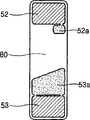
参考图5和6,图5说明了使用具有纯铝的电极在热处理之后的TFT的横断面图,图6是热处理之后的该TFT的顶视图。图5说明了在450℃热处理之后,半导体层80布置在S/D电极和引线52与53的下面并且与它们相连,它们中的每个都具有三层结构,即钛层(Ti)(厚度500埃)232/纯铝层(厚度4000埃)231/Ti层(厚度500埃)233。如图5和6所示,在加热时纯铝层231中的Al向半导体层80扩散并扩散到其中,从而在半导体层80中形成扩散缺陷部分52a和53a。即使在纯铝层231和半导体层80之间插入了Ti层233,纯铝层231中的Al还是会扩散到半导体层80中,其原因在于,Ti层233是非常薄的薄膜和/或根据半导体层80的上表面结构在Ti层233中存在无Ti区。这样,在加热时,在TFT的电极的纯铝层231和半导体层80之间的薄钛层233并不能阻挡纯铝层231中的铝扩散进入半导体层80中并且损伤部分半导体层80。应当理解的是,当加热时,在钛层和纯铝层之间的TiN扩散层的存在将不能阻挡铝扩散到半导体层80中。Referring to FIGS. 5 and 6, FIG. 5 illustrates a cross-sectional view of a TFT after heat treatment using electrodes having pure aluminum, and FIG. 6 is a top view of the TFT after heat treatment. 5 illustrates that after a heat treatment at 450° C., a
最终的扩散缺陷部分52a和53a可以产生同将纯铝直接沉积在半导体层80上时的相同结果。缺陷部分52a和53a会阻碍TFT的源极和漏极之间的正常导电沟道的形成。另外缺陷部分52a和53a会造成源极和漏极之间的短路,导致TFT不能正常工作。尽管图5和6说明了第二TFT50的源极52和漏极53,但是也同样适用于第一TFT10。The resulting
在下文中,将参考图2和图7到10来详细地说明S/D电极和引线的结构。根据本发明的该实施方案,第一和第二栅极11和53与第二导线30是使用相同的材料同时形成的。第一和第二源极12和52,第一和第二漏极13和53,第一导线30,以及第三导线70是使用相同的材料同时形成的。因为根据制作工艺可以改变用于这些导电的组成单元的形成顺序和材料,所以它们并不局限于在本发明的实施方案中的说明。Hereinafter, the structures of the S/D electrodes and lead wires will be described in detail with reference to FIG. 2 and FIGS. 7 to 10 . According to this embodiment of the present invention, the first and
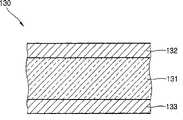
根据本发明的该实施方案,S/D电极和引线130中的至少一个是由铝(Al)合金层131和形成在该铝(Al)合金层131的相应上下表面的钛层(Ti)132和133制得的。任选的是,在图10示出的另一实施方案中,扩散阻挡层138和139是由氮化钛(TiN)构成的,该扩散阻挡层138和139例如可以被插入在铝合金层131和相应的钛层132和/或133之间。当在电极结构中使用跟纯铝相对的铝合金时,就能够在热处理期间防止铝扩散。According to this embodiment of the present invention, at least one of the S/D electrode and the
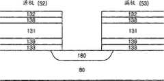
优选的是,铝合金层131是由含有0.1到5wt%,优选的是含有2wt%的从硅(Si)、铜(Cu)、钕(Nd)、铂(Pt)和镍(Ni)中选择的至少一种元素来构成的。据经验确定,当根据图10中所示的本发明的实施方案的S/D电极和引线具有5层结构时,即Ti层(厚度250埃)132/TiN层(厚度250埃)138/铝合金层(厚度4000埃)131/TiN层(厚度250埃)139/Ti层(厚度250埃)133,即使在450℃进行热处理之后,铝合金层131中的铝也不会扩散向半导体层80。因此如图9所示,半导体层80没有缺陷部分,使得在TFT工作期间形成导电沟道180。这样由于在电极结构中使用了铝合金层而不是在电极结构中使用纯铝而得到了好的结果。当如图8所示,S/D电极和引线具有三层结构时,即Ti层(厚度500埃)132/铝合金层(厚度4000埃)131/Ti层(厚度500埃)133,可以获得相同的结果。换句话说,跟图10的结构一样,图8的结构产生如图9中的没有缺陷区域52a和53a的半导体层80。Preferably, the
可以理解的是,除了在电极堆叠中用铝合金层代替纯铝层之外,在同图6的经验数据相同的实验条件下也可以获得图9的经验数据。换句话说,在除了用铝合金层131代替纯铝层231之外,其他所有的参数保持不变,这样就可以获得图6和9的结果。It can be understood that the empirical data of FIG. 9 can also be obtained under the same experimental conditions as the empirical data of FIG. 6 except that the aluminum alloy layer is used in the electrode stack instead of the pure aluminum layer. In other words, except that the
应当理解的是,使用钛层132和133而不是仅用铝合金层131,因为钛层132和133可以起到在热处理期间防止铝小丘形成的作用。It should be understood that the titanium layers 132 and 133 are used rather than just the
在另一实施方案中,使用了图10的5层电极堆叠,在该电极堆叠中为了避免在热处理过程中形成不需要的TiAl3,在每个钛层132(133)和铝合金层131之间插入了TiN扩散阻挡层138(139)。TiAl3大大地提高了电极和导线的电阻率。因而,TiN扩散阻挡层138和139防止了TiAl3的形成,这样就保持了电极和通向TFT的导线的电阻率低。这一点在大的平板显示器中特别重要,在该大的平板显示器中电极和引线的低电阻率可以防止非均匀像素显示分布。尽管结合具有源极52和漏极53的第二TFT50讨论了图8,9和10,但是图8,9和10的新颖的结构同样适用于第一TFT10。In another embodiment, the 5-layer electrode stack of FIG. 10 is used, in which in order to avoid the formation of unwanted TiAl3 during heat treatment, between each titanium layer 132 (133) and the aluminum alloy layer 131 A TiN diffusion barrier layer 138 (139) is interposed therebetween. TiAl3 greatly increases the resistivity of electrodes and wires. Thus, the TiN diffusion barrier layers 138 and 139 prevent the formation ofTiAl3 , thus keeping the resistivity of the electrodes and wires leading to the TFT low. This is especially important in large flat panel displays where the low resistivity of the electrodes and leads prevents non-uniform pixel display distribution. Although FIGS. 8 , 9 and 10 are discussed in connection with a
TiN扩散阻挡层138和139最佳厚度是250埃。如果扩散阻挡层的厚度太薄,可以产生铝扩散,导致在热处理期间形成TiAl3。另一方面,如果TiN扩散阻挡层太厚,则由于不必要的厚的TiN层而使得制作成本变得不必要地昂贵。优选的是,TiN层138和139含有5到85wt%的氮。The preferred thickness of TiN diffusion barrier layers 138 and 139 is 250 Angstroms. If the thickness of the diffusion barrier layer is too thin, aluminum diffusion can occur, leading to the formation ofTiAl3 during heat treatment. On the other hand, if the TiN diffusion barrier layer is too thick, fabrication becomes unnecessarily expensive due to the unnecessarily thick TiN layer. Preferably, TiN layers 138 and 139 contain 5 to 85 wt% nitrogen.
在制作图10的电极堆叠130的方法中,在氩气(Ar)气氛下,通过DC-磁控管溅射来沉积铝合金层131和钛层132和133。在氩气(Ar)和氮气(N2)的混合气体气氛下,通过反应溅射来沉积TiN层138和139。通过使用高频增强等离子体的干法刻蚀来刻蚀这些沉积的结构,形成预定图案的S/D电极和引线。In the method of fabricating the
应当理解的是,图5到10讨论了第二TFT50和第二源极52以及第二漏极53,图5到10和在上面讨论图5到10中所讨论的概念同样适用于具有第一源极12和第一漏极13的第一TFT10。It should be understood that FIGS. 5 to 10 discuss a
本发明提供了一种附着于TFT中的半导体层的电极的新颖结构,在热处理时该结构不会在半导体层中形成缺陷区域。另外,保持了低的电阻率。其他的实施方案包括提供钛层以防止在热处理过程中形成铝小丘。另外的实施方案包括在铝合金层和钛层之间提供TiN扩散层以防止在热处理时形成高电阻的TiAl3。通过在TFT晶体管中使用本发明的新颖的电极结构,保持了晶体管的完整性并且降低了导线和电极的电阻率,从而形成在像素之间具有均匀发光的大的平板显示器。The present invention provides a novel structure of an electrode attached to a semiconductor layer in a TFT that does not form defect regions in the semiconductor layer upon heat treatment. In addition, the resistivity is kept low. Other embodiments include providing a titanium layer to prevent the formation of aluminum hillocks during heat treatment. Additional embodiments include providing a TiN diffusion layer between the aluminum alloy layer and the titanium layer to prevent the formation of highly resistiveTiAl3 upon heat treatment. By using the novel electrode structure of the present invention in a TFT transistor, the integrity of the transistor is maintained and the resistivity of the wires and electrodes is reduced, resulting in a large flat panel display with uniform light emission between pixels.
虽然参考实例性实施方案,特别示出和说明了本发明,但是本领域的普通技术人员将能理解在不偏离下面权利要求书所限定的本发明的精神和范围的情况下,可以进行各种形式和细节上的修改。While the invention has been particularly shown and described with reference to exemplary embodiments, it will be understood by those skilled in the art that various modifications may be made without departing from the spirit and scope of the invention as defined in the following claims. Modifications in form and detail.
Claims (20)
Applications Claiming Priority (3)
| Application Number | Priority Date | Filing Date | Title |
|---|---|---|---|
| KR15357/2003 | 2003-03-12 | ||
| KR1020030015357AKR100669688B1 (en) | 2003-03-12 | 2003-03-12 | Thin film transistor and flat panel display device having same |
| KR15357/03 | 2003-03-12 |
Publications (2)
| Publication Number | Publication Date |
|---|---|
| CN1530725Atrue CN1530725A (en) | 2004-09-22 |
| CN100351691C CN100351691C (en) | 2007-11-28 |
Family
ID=32768636
Family Applications (1)
| Application Number | Title | Priority Date | Filing Date |
|---|---|---|---|
| CNB2004100287328AExpired - LifetimeCN100351691C (en) | 2003-03-12 | 2004-03-12 | Conductive element of thin membrane transistor in planar displaying device |
Country Status (5)
| Country | Link |
|---|---|
| US (2) | US20040183072A1 (en) |
| EP (1) | EP1458030A3 (en) |
| JP (1) | JP2004282066A (en) |
| KR (1) | KR100669688B1 (en) |
| CN (1) | CN100351691C (en) |
Cited By (6)
| Publication number | Priority date | Publication date | Assignee | Title |
|---|---|---|---|---|
| US7492028B2 (en) | 2005-02-18 | 2009-02-17 | Semiconductor Energy Laboratory Co., Ltd. | Photoelectric conversion device and manufacturing method of the same, and a semiconductor device |
| CN104685635A (en)* | 2012-10-01 | 2015-06-03 | 夏普株式会社 | Semiconductor device |
| CN106531768A (en)* | 2016-12-07 | 2017-03-22 | 厦门天马微电子有限公司 | Organic electroluminescence display panel and preparation method thereof |
| CN109671717A (en)* | 2017-10-17 | 2019-04-23 | 三星显示有限公司 | Metal wire and thin film transistor (TFT) |
| CN111490076A (en)* | 2019-01-25 | 2020-08-04 | 三星显示有限公司 | Conductive line, display device including the same, and method of manufacturing the display device |
| CN111529048A (en)* | 2013-12-18 | 2020-08-14 | 诺服塞尔有限公司 | Apparatus and method for vaporizing tissue |
Families Citing this family (17)
| Publication number | Priority date | Publication date | Assignee | Title |
|---|---|---|---|---|
| JP4038485B2 (en)* | 2003-03-12 | 2008-01-23 | 三星エスディアイ株式会社 | Flat panel display device with thin film transistor |
| US7683370B2 (en) | 2005-08-17 | 2010-03-23 | Kobe Steel, Ltd. | Source/drain electrodes, transistor substrates and manufacture methods, thereof, and display devices |
| KR100799824B1 (en)* | 2005-08-17 | 2008-01-31 | 가부시키가이샤 고베 세이코쇼 | Source / drain electrodes, transistor substrates and methods of manufacturing the same, and display devices |
| KR101251351B1 (en)* | 2005-12-28 | 2013-04-05 | 삼성디스플레이 주식회사 | Thin film transistor substrate, method for making the substrate and display panel having the substrate |
| KR100774950B1 (en)* | 2006-01-19 | 2007-11-09 | 엘지전자 주식회사 | Electroluminescent element |
| JP4926169B2 (en)* | 2006-04-27 | 2012-05-09 | 株式会社アルバック | Method for manufacturing composite display device |
| JP5214858B2 (en) | 2006-06-22 | 2013-06-19 | 三菱電機株式会社 | TFT array substrate and manufacturing method thereof |
| AT12768U1 (en) | 2010-03-29 | 2012-11-15 | Ctr Carinthian Tech Res Ag | HIGH TEMPERATURE RESISTANT, ELECTRICALLY CONDUCTIVE THIN FILMS |
| JP5016712B2 (en)* | 2010-09-21 | 2012-09-05 | 三井金属鉱業株式会社 | Electrode foil and organic device |
| US8841733B2 (en) | 2011-05-17 | 2014-09-23 | United Microelectronics Corp. | Semiconductor device and method of fabricating the same |
| JP2013084907A (en) | 2011-09-28 | 2013-05-09 | Kobe Steel Ltd | Wiring structure for display device |
| EP2993963A4 (en)* | 2013-05-01 | 2016-12-14 | Konica Minolta Inc | ORGANIC ELECTROLUMINESCENT ELEMENT |
| TWI535034B (en)* | 2014-01-29 | 2016-05-21 | 友達光電股份有限公司 | Pixel structure and its making method |
| US9548349B2 (en)* | 2014-06-25 | 2017-01-17 | International Business Machines Corporation | Semiconductor device with metal extrusion formation |
| CN104241392B (en)* | 2014-07-14 | 2017-07-14 | 京东方科技集团股份有限公司 | A kind of thin film transistor (TFT) and preparation method thereof, display base plate and display device |
| KR102839408B1 (en) | 2019-01-17 | 2025-07-28 | 삼성디스플레이 주식회사 | Display devices and manufacturing method thereof |
| KR102819170B1 (en)* | 2019-02-18 | 2025-06-12 | 삼성디스플레이 주식회사 | Display device and method of manufacturing the display device |
Family Cites Families (62)
| Publication number | Priority date | Publication date | Assignee | Title |
|---|---|---|---|---|
| US4153529A (en)* | 1975-04-21 | 1979-05-08 | Hughes Aircraft Company | Means and method for inducing uniform parallel alignment of liquid crystal material in a liquid crystal cell |
| DE8232492U1 (en)* | 1982-11-19 | 1986-03-27 | Siemens AG, 1000 Berlin und 8000 München | Amorphous silicon solar cell |
| US5278099A (en)* | 1985-05-13 | 1994-01-11 | Kabushiki Kaisha Toshiba | Method for manufacturing a semiconductor device having wiring electrodes |
| US4646424A (en)* | 1985-08-02 | 1987-03-03 | General Electric Company | Deposition and hardening of titanium gate electrode material for use in inverted thin film field effect transistors |
| US4933296A (en)* | 1985-08-02 | 1990-06-12 | General Electric Company | N+ amorphous silicon thin film transistors for matrix addressed liquid crystal displays |
| US4782380A (en)* | 1987-01-22 | 1988-11-01 | Advanced Micro Devices, Inc. | Multilayer interconnection for integrated circuit structure having two or more conductive metal layers |
| US4910580A (en)* | 1987-08-27 | 1990-03-20 | Siemens Aktiengesellschaft | Method for manufacturing a low-impedance, planar metallization composed of aluminum or of an aluminum alloy |
| US4778258A (en)* | 1987-10-05 | 1988-10-18 | General Electric Company | Protective tab structure for use in the fabrication of matrix addressed thin film transistor liquid crystal displays |
| JPH0666287B2 (en)* | 1988-07-25 | 1994-08-24 | 富士通株式会社 | Method for manufacturing semiconductor device |
| US5244820A (en)* | 1990-03-09 | 1993-09-14 | Tadashi Kamata | Semiconductor integrated circuit device, method for producing the same, and ion implanter for use in the method |
| US5243202A (en)* | 1990-04-25 | 1993-09-07 | Casio Computer Co., Ltd. | Thin-film transistor and a liquid crystal matrix display device using thin-film transistors of this type |
| US5345108A (en)* | 1991-02-26 | 1994-09-06 | Nec Corporation | Semiconductor device having multi-layer electrode wiring |
| JP2533414B2 (en)* | 1991-04-09 | 1996-09-11 | 三菱電機株式会社 | Wiring connection structure of semiconductor integrated circuit device and manufacturing method thereof |
| US5485019A (en)* | 1992-02-05 | 1996-01-16 | Semiconductor Energy Laboratory Co., Ltd. | Semiconductor device and method for forming the same |
| JP3587537B2 (en)* | 1992-12-09 | 2004-11-10 | 株式会社半導体エネルギー研究所 | Semiconductor device |
| JPH06188265A (en)* | 1992-12-22 | 1994-07-08 | Matsushita Electric Ind Co Ltd | Semiconductor device and manufacture thereof |
| JPH06250211A (en)* | 1993-02-23 | 1994-09-09 | Hitachi Ltd | Liquid crystal display substrate and its production |
| US5427666A (en)* | 1993-09-09 | 1995-06-27 | Applied Materials, Inc. | Method for in-situ cleaning a Ti target in a Ti + TiN coating process |
| DE19515564B4 (en)* | 1994-04-28 | 2008-07-03 | Denso Corp., Kariya | Electrode for a semiconductor device and method of making the same |
| US5742468A (en)* | 1994-10-24 | 1998-04-21 | Olympus Optical Co., Ltd. | Electric charge generator for use in an apparatus for producing an electrostatic latent image |
| US5538921A (en)* | 1994-12-22 | 1996-07-23 | At&T Corp. | Integrated circuit fabrication |
| US6790714B2 (en)* | 1995-07-03 | 2004-09-14 | Sanyo Electric Co., Ltd. | Semiconductor device, display device and method of fabricating the same |
| JP3744980B2 (en)* | 1995-07-27 | 2006-02-15 | 株式会社半導体エネルギー研究所 | Semiconductor device |
| US5747879A (en)* | 1995-09-29 | 1998-05-05 | Intel Corporation | Interface between titanium and aluminum-alloy in metal stack for integrated circuit |
| JP2850850B2 (en)* | 1996-05-16 | 1999-01-27 | 日本電気株式会社 | Method for manufacturing semiconductor device |
| US5759916A (en)* | 1996-06-24 | 1998-06-02 | Taiwan Semiconductor Manufacturing Company Ltd | Method for forming a void-free titanium nitride anti-reflective coating(ARC) layer upon an aluminum containing conductor layer |
| JP3728755B2 (en)* | 1996-10-22 | 2005-12-21 | セイコーエプソン株式会社 | Active matrix LCD panel |
| JP3480791B2 (en)* | 1996-12-25 | 2003-12-22 | 三菱電機株式会社 | Method for manufacturing thin film transistor |
| TW531684B (en)* | 1997-03-31 | 2003-05-11 | Seiko Epson Corporatoin | Display device and method for manufacturing the same |
| US5943601A (en)* | 1997-04-30 | 1999-08-24 | International Business Machines Corporation | Process for fabricating a metallization structure |
| US6028003A (en)* | 1997-07-03 | 2000-02-22 | Motorola, Inc. | Method of forming an interconnect structure with a graded composition using a nitrided target |
| US5893752A (en)* | 1997-12-22 | 1999-04-13 | Motorola, Inc. | Process for forming a semiconductor device |
| DE19734434C1 (en)* | 1997-08-08 | 1998-12-10 | Siemens Ag | Semiconductor body with reverse-side metallisation e.g. for power semiconductor |
| JP3221373B2 (en)* | 1997-10-24 | 2001-10-22 | 日本電気株式会社 | Patterning method for laminated wiring |
| JPH11186190A (en)* | 1997-12-25 | 1999-07-09 | Sharp Corp | Method for manufacturing semiconductor device |
| JP3980156B2 (en)* | 1998-02-26 | 2007-09-26 | 株式会社半導体エネルギー研究所 | Active matrix display device |
| KR100301530B1 (en)* | 1998-06-30 | 2001-10-19 | 한신혁 | Mehtod for forming inter layer insulting film in the semiconductor device |
| EP0986084A3 (en)* | 1998-09-11 | 2004-01-21 | Pioneer Corporation | Electron emission device and display apparatus using the same |
| JP2000150520A (en)* | 1998-11-10 | 2000-05-30 | Internatl Business Mach Corp <Ibm> | Interconnects and methods of manufacturing interconnects |
| US6410986B1 (en)* | 1998-12-22 | 2002-06-25 | Agere Systems Guardian Corp. | Multi-layered titanium nitride barrier structure |
| US6380625B2 (en)* | 1999-01-13 | 2002-04-30 | Advanced Micro Devices, Inc. | Semiconductor interconnect barrier and manufacturing method thereof |
| JP3916334B2 (en)* | 1999-01-13 | 2007-05-16 | シャープ株式会社 | Thin film transistor |
| US6534393B1 (en)* | 1999-01-25 | 2003-03-18 | Chartered Semiconductor Manufacturing Ltd. | Method for fabricating local metal interconnections with low contact resistance and gate electrodes with improved electrical conductivity |
| US6224942B1 (en)* | 1999-08-19 | 2001-05-01 | Micron Technology, Inc. | Method of forming an aluminum comprising line having a titanium nitride comprising layer thereon |
| JP2001060590A (en)* | 1999-08-20 | 2001-03-06 | Denso Corp | Electric wiring of semiconductor device and manufacture thereof |
| JP2001147424A (en)* | 1999-11-19 | 2001-05-29 | Hitachi Ltd | Insulating substrate for forming conductive thin film and liquid crystal display device using this insulating substrate |
| JP2001250956A (en)* | 2000-03-08 | 2001-09-14 | Semiconductor Energy Lab Co Ltd | Semiconductor device |
| US6365927B1 (en)* | 2000-04-03 | 2002-04-02 | Symetrix Corporation | Ferroelectric integrated circuit having hydrogen barrier layer |
| TW447138B (en)* | 2000-04-28 | 2001-07-21 | Unipac Optoelectronics Corp | Manufacturing method of thin-film transistor |
| TW538246B (en)* | 2000-06-05 | 2003-06-21 | Semiconductor Energy Lab | Display panel, display panel inspection method, and display panel manufacturing method |
| JP4014831B2 (en)* | 2000-09-04 | 2007-11-28 | 株式会社半導体エネルギー研究所 | EL display device and driving method thereof |
| TW550530B (en)* | 2000-10-27 | 2003-09-01 | Semiconductor Energy Lab | Display device and method of driving the same |
| US6503641B2 (en)* | 2000-12-18 | 2003-01-07 | International Business Machines Corporation | Interconnects with Ti-containing liners |
| JP2002202527A (en)* | 2000-12-28 | 2002-07-19 | Nec Corp | Active matrix type liquid crystal display device |
| KR100370286B1 (en)* | 2000-12-29 | 2003-01-29 | 삼성에스디아이 주식회사 | circuit of electroluminescent display pixel for voltage driving |
| TW490857B (en)* | 2001-02-05 | 2002-06-11 | Samsung Electronics Co Ltd | Thin film transistor array substrate for liquid crystal display and method of fabricating same |
| US6440752B1 (en)* | 2001-03-26 | 2002-08-27 | Sharp Laboratories Of America, Inc. | Electrode materials with improved hydrogen degradation resistance and fabrication method |
| KR100374228B1 (en)* | 2001-03-28 | 2003-03-03 | 주식회사 하이닉스반도체 | Method for forming a metal line |
| JP2003015105A (en)* | 2001-06-28 | 2003-01-15 | Hitachi Ltd | Image display device |
| JP2003017706A (en)* | 2001-07-02 | 2003-01-17 | Idemitsu Kosan Co Ltd | TFT substrate, liquid crystal display device using the same, and method of manufacturing the same |
| EP1343206B1 (en)* | 2002-03-07 | 2016-10-26 | Semiconductor Energy Laboratory Co., Ltd. | Light emitting apparatus, electronic apparatus, illuminating device and method of fabricating the light emitting apparatus |
| JP4334811B2 (en)* | 2002-03-28 | 2009-09-30 | 株式会社ルネサステクノロジ | Manufacturing method of semiconductor device |
- 2003
- 2003-03-12KRKR1020030015357Apatent/KR100669688B1/ennot_activeExpired - Lifetime
- 2004
- 2004-01-30USUS10/767,281patent/US20040183072A1/ennot_activeAbandoned
- 2004-02-18EPEP04250862Apatent/EP1458030A3/ennot_activeWithdrawn
- 2004-03-09JPJP2004066092Apatent/JP2004282066A/enactivePending
- 2004-03-12CNCNB2004100287328Apatent/CN100351691C/ennot_activeExpired - Lifetime
- 2005
- 2005-09-06USUS11/218,496patent/US20060011914A1/ennot_activeAbandoned
Cited By (12)
| Publication number | Priority date | Publication date | Assignee | Title |
|---|---|---|---|---|
| US7492028B2 (en) | 2005-02-18 | 2009-02-17 | Semiconductor Energy Laboratory Co., Ltd. | Photoelectric conversion device and manufacturing method of the same, and a semiconductor device |
| US7936037B2 (en) | 2005-02-18 | 2011-05-03 | Semiconductor Energy Laboratory Co., Ltd. | Photoelectric conversion device and manufacturing method of the same, and a semiconductor device |
| CN1832207B (en)* | 2005-02-18 | 2011-05-18 | 株式会社半导体能源研究所 | Photoelectric conversion device, manufacturing method thereof, and semiconductor device |
| CN102176488B (en)* | 2005-02-18 | 2013-04-03 | 株式会社半导体能源研究所 | Photoelectric conversion device, manufacturing method thereof, and semiconductor device |
| CN104685635A (en)* | 2012-10-01 | 2015-06-03 | 夏普株式会社 | Semiconductor device |
| CN104685635B (en)* | 2012-10-01 | 2017-05-17 | 夏普株式会社 | Semiconductor device |
| CN111529048A (en)* | 2013-12-18 | 2020-08-14 | 诺服塞尔有限公司 | Apparatus and method for vaporizing tissue |
| CN111529048B (en)* | 2013-12-18 | 2024-03-26 | 诺服塞尔有限公司 | Equipment and methods for vaporizing tissue |
| CN106531768A (en)* | 2016-12-07 | 2017-03-22 | 厦门天马微电子有限公司 | Organic electroluminescence display panel and preparation method thereof |
| CN109671717A (en)* | 2017-10-17 | 2019-04-23 | 三星显示有限公司 | Metal wire and thin film transistor (TFT) |
| CN111490076A (en)* | 2019-01-25 | 2020-08-04 | 三星显示有限公司 | Conductive line, display device including the same, and method of manufacturing the display device |
| CN111490076B (en)* | 2019-01-25 | 2025-05-13 | 三星显示有限公司 | Wire, display device including the wire, and method for manufacturing the display device |
Also Published As
| Publication number | Publication date |
|---|---|
| EP1458030A3 (en) | 2006-03-15 |
| EP1458030A2 (en) | 2004-09-15 |
| JP2004282066A (en) | 2004-10-07 |
| KR100669688B1 (en) | 2007-01-18 |
| US20040183072A1 (en) | 2004-09-23 |
| CN100351691C (en) | 2007-11-28 |
| US20060011914A1 (en) | 2006-01-19 |
| KR20040080531A (en) | 2004-09-20 |
Similar Documents
| Publication | Publication Date | Title |
|---|---|---|
| CN1530725A (en) | Novel conducting element for thin-film transistors used in flat-panel displays | |
| CN1246824C (en) | Display device | |
| CN105810852B (en) | A kind of production method of organic light emitting display panel | |
| CN1735290B (en) | Electroluminescence display device and method of manufacturing the same | |
| CN1440224A (en) | Active matrix organic electrogenic luminating display device and manufacture thereof | |
| CN101887867B (en) | The manufacture method of organic light emitting diode display | |
| JP2005235491A (en) | Image display device | |
| CN1543269A (en) | Conductor Design in Electroluminescent Display Devices | |
| TW200302439A (en) | Light emitting device and method of manufacturing the same | |
| CN100419550C (en) | Novel conductive material for thin-film transistors used in flat-panel displays | |
| TW200541379A (en) | Organic light-emmiting display device and fabricating thereof | |
| WO2010053183A1 (en) | Reflective anode and wiring film for organic el display device | |
| KR100864001B1 (en) | Organic electroluminescent devices | |
| JP2002246185A (en) | Organic electroluminescent device | |
| JP2010225293A (en) | Functional element and display device | |
| CN1446033A (en) | Electroluminescence display device and manufacturing method thereof | |
| TWI455302B (en) | Organic electroluminescence device and method for manufacturing the same | |
| KR100553747B1 (en) | Thin film transistor and flat display device comprising it | |
| CN1434428A (en) | Display | |
| US8927970B2 (en) | Organic electroluminescence device and method for manufacturing the same | |
| CN1441627A (en) | Electroluminescence display device | |
| US8817200B2 (en) | Liquid crystal display device comprising a TFT with a barrier metal formed of a first layer and a second layer wherein the first layer is denser than the second layer | |
| KR101104419B1 (en) | Active organic light emitting device and manufacturing method | |
| JP2004241160A (en) | Organic electroluminescent device | |
| JP2003109771A (en) | Organic electroluminescence device and method of manufacturing the same |
Legal Events
| Date | Code | Title | Description |
|---|---|---|---|
| C06 | Publication | ||
| PB01 | Publication | ||
| C10 | Entry into substantive examination | ||
| SE01 | Entry into force of request for substantive examination | ||
| C14 | Grant of patent or utility model | ||
| GR01 | Patent grant | ||
| C41 | Transfer of patent application or patent right or utility model | ||
| TR01 | Transfer of patent right | Effective date of registration:20090116 Address after:Gyeonggi Do Korea Suwon Patentee after:Samsung Mobile Display Co.,Ltd. Address before:Gyeonggi Do Korea Suwon Patentee before:Samsung SDI Co.,Ltd. | |
| ASS | Succession or assignment of patent right | Owner name:SAMSUNG MOBILE DISPLAY CO., LTD. Free format text:FORMER OWNER: SAMSUNG SDI CO., LTD. Effective date:20090116 | |
| ASS | Succession or assignment of patent right | Owner name:SAMSUNG DISPLAY CO., LTD. Free format text:FORMER OWNER: SAMSUNG MOBILE DISPLAY CO., LTD. Effective date:20120928 | |
| C41 | Transfer of patent application or patent right or utility model | ||
| TR01 | Transfer of patent right | Effective date of registration:20120928 Address after:Gyeonggi Do Korea Suwon Patentee after:SAMSUNG DISPLAY Co.,Ltd. Address before:Gyeonggi Do Korea Suwon Patentee before:Samsung Mobile Display Co.,Ltd. | |
| CX01 | Expiry of patent term | Granted publication date:20071128 | |
| CX01 | Expiry of patent term |