CN1530697A - Liquid crystal display device and electronic equipment - Google Patents
Liquid crystal display device and electronic equipmentDownload PDFInfo
- Publication number
- CN1530697A CN1530697ACNA2004100064476ACN200410006447ACN1530697ACN 1530697 ACN1530697 ACN 1530697ACN A2004100064476 ACNA2004100064476 ACN A2004100064476ACN 200410006447 ACN200410006447 ACN 200410006447ACN 1530697 ACN1530697 ACN 1530697A
- Authority
- CN
- China
- Prior art keywords
- liquid crystal
- transmissive display
- display area
- crystal layer
- area
- Prior art date
- Legal status (The legal status is an assumption and is not a legal conclusion. Google has not performed a legal analysis and makes no representation as to the accuracy of the status listed.)
- Granted
Links
- 239000004973liquid crystal related substanceSubstances0.000titleclaimsabstractdescription156
- 239000000758substrateSubstances0.000claimsabstractdescription57
- 230000007547defectEffects0.000abstractdescription9
- 206010047571Visual impairmentDiseases0.000abstractdescription5
- 239000010408filmSubstances0.000description43
- 230000005684electric fieldEffects0.000description9
- 239000011159matrix materialSubstances0.000description7
- 239000000049pigmentSubstances0.000description5
- 230000015572biosynthetic processEffects0.000description4
- 238000010586diagramMethods0.000description4
- 230000001105regulatory effectEffects0.000description4
- 239000010409thin filmSubstances0.000description4
- 238000002834transmittanceMethods0.000description4
- 230000000694effectsEffects0.000description3
- 239000000463materialSubstances0.000description3
- 239000004065semiconductorSubstances0.000description3
- 239000004925Acrylic resinSubstances0.000description2
- 229920000178Acrylic resinPolymers0.000description2
- 239000004642PolyimideSubstances0.000description2
- 229910052782aluminiumInorganic materials0.000description2
- XAGFODPZIPBFFR-UHFFFAOYSA-NaluminiumChemical compound[Al]XAGFODPZIPBFFR-UHFFFAOYSA-N0.000description2
- 239000000470constituentSubstances0.000description2
- 210000002858crystal cellAnatomy0.000description2
- 208000037265diseases, disorders, signs and symptomsDiseases0.000description2
- 239000011521glassSubstances0.000description2
- AMGQUBHHOARCQH-UHFFFAOYSA-Nindium;oxotinChemical compound[In].[Sn]=OAMGQUBHHOARCQH-UHFFFAOYSA-N0.000description2
- 229910052751metalInorganic materials0.000description2
- 239000002184metalSubstances0.000description2
- 238000000034methodMethods0.000description2
- 230000003287optical effectEffects0.000description2
- 229920001721polyimidePolymers0.000description2
- 239000010453quartzSubstances0.000description2
- VYPSYNLAJGMNEJ-UHFFFAOYSA-Nsilicon dioxideInorganic materialsO=[Si]=OVYPSYNLAJGMNEJ-UHFFFAOYSA-N0.000description2
- 230000005540biological transmissionEffects0.000description1
- 239000003990capacitorSubstances0.000description1
- 210000004027cellAnatomy0.000description1
- 239000003086colorantSubstances0.000description1
- 230000001276controlling effectEffects0.000description1
- 239000003989dielectric materialSubstances0.000description1
- 230000001747exhibiting effectEffects0.000description1
- 238000010030laminatingMethods0.000description1
- 238000004519manufacturing processMethods0.000description1
- 229910021420polycrystalline siliconInorganic materials0.000description1
- 229920005591polysiliconPolymers0.000description1
- 230000000717retained effectEffects0.000description1
- 238000000926separation methodMethods0.000description1
- 229910052709silverInorganic materials0.000description1
- 239000004332silverSubstances0.000description1
Images


Classifications
- G—PHYSICS
- G02—OPTICS
- G02F—OPTICAL DEVICES OR ARRANGEMENTS FOR THE CONTROL OF LIGHT BY MODIFICATION OF THE OPTICAL PROPERTIES OF THE MEDIA OF THE ELEMENTS INVOLVED THEREIN; NON-LINEAR OPTICS; FREQUENCY-CHANGING OF LIGHT; OPTICAL LOGIC ELEMENTS; OPTICAL ANALOGUE/DIGITAL CONVERTERS
- G02F1/00—Devices or arrangements for the control of the intensity, colour, phase, polarisation or direction of light arriving from an independent light source, e.g. switching, gating or modulating; Non-linear optics
- G02F1/01—Devices or arrangements for the control of the intensity, colour, phase, polarisation or direction of light arriving from an independent light source, e.g. switching, gating or modulating; Non-linear optics for the control of the intensity, phase, polarisation or colour
- G02F1/13—Devices or arrangements for the control of the intensity, colour, phase, polarisation or direction of light arriving from an independent light source, e.g. switching, gating or modulating; Non-linear optics for the control of the intensity, phase, polarisation or colour based on liquid crystals, e.g. single liquid crystal display cells
- G02F1/133—Constructional arrangements; Operation of liquid crystal cells; Circuit arrangements
- G02F1/1333—Constructional arrangements; Manufacturing methods
- G02F1/1337—Surface-induced orientation of the liquid crystal molecules, e.g. by alignment layers
- G02F1/133753—Surface-induced orientation of the liquid crystal molecules, e.g. by alignment layers with different alignment orientations or pretilt angles on a same surface, e.g. for grey scale or improved viewing angle
- E—FIXED CONSTRUCTIONS
- E04—BUILDING
- E04D—ROOF COVERINGS; SKY-LIGHTS; GUTTERS; ROOF-WORKING TOOLS
- E04D1/00—Roof covering by making use of tiles, slates, shingles, or other small roofing elements
- E04D1/30—Special roof-covering elements, e.g. ridge tiles, gutter tiles, gable tiles, ventilation tiles
- E04D2001/301—Special roof-covering elements, e.g. ridge tiles, gutter tiles, gable tiles, ventilation tiles at roof edges, e.g. intersections with walls
- E04D2001/303—Eave tiles
- G—PHYSICS
- G02—OPTICS
- G02F—OPTICAL DEVICES OR ARRANGEMENTS FOR THE CONTROL OF LIGHT BY MODIFICATION OF THE OPTICAL PROPERTIES OF THE MEDIA OF THE ELEMENTS INVOLVED THEREIN; NON-LINEAR OPTICS; FREQUENCY-CHANGING OF LIGHT; OPTICAL LOGIC ELEMENTS; OPTICAL ANALOGUE/DIGITAL CONVERTERS
- G02F1/00—Devices or arrangements for the control of the intensity, colour, phase, polarisation or direction of light arriving from an independent light source, e.g. switching, gating or modulating; Non-linear optics
- G02F1/01—Devices or arrangements for the control of the intensity, colour, phase, polarisation or direction of light arriving from an independent light source, e.g. switching, gating or modulating; Non-linear optics for the control of the intensity, phase, polarisation or colour
- G02F1/13—Devices or arrangements for the control of the intensity, colour, phase, polarisation or direction of light arriving from an independent light source, e.g. switching, gating or modulating; Non-linear optics for the control of the intensity, phase, polarisation or colour based on liquid crystals, e.g. single liquid crystal display cells
- G02F1/133—Constructional arrangements; Operation of liquid crystal cells; Circuit arrangements
- G02F1/1333—Constructional arrangements; Manufacturing methods
- G02F1/1335—Structural association of cells with optical devices, e.g. polarisers or reflectors
- G02F1/133553—Reflecting elements
- G02F1/133555—Transflectors
- G—PHYSICS
- G02—OPTICS
- G02F—OPTICAL DEVICES OR ARRANGEMENTS FOR THE CONTROL OF LIGHT BY MODIFICATION OF THE OPTICAL PROPERTIES OF THE MEDIA OF THE ELEMENTS INVOLVED THEREIN; NON-LINEAR OPTICS; FREQUENCY-CHANGING OF LIGHT; OPTICAL LOGIC ELEMENTS; OPTICAL ANALOGUE/DIGITAL CONVERTERS
- G02F1/00—Devices or arrangements for the control of the intensity, colour, phase, polarisation or direction of light arriving from an independent light source, e.g. switching, gating or modulating; Non-linear optics
- G02F1/01—Devices or arrangements for the control of the intensity, colour, phase, polarisation or direction of light arriving from an independent light source, e.g. switching, gating or modulating; Non-linear optics for the control of the intensity, phase, polarisation or colour
- G02F1/13—Devices or arrangements for the control of the intensity, colour, phase, polarisation or direction of light arriving from an independent light source, e.g. switching, gating or modulating; Non-linear optics for the control of the intensity, phase, polarisation or colour based on liquid crystals, e.g. single liquid crystal display cells
- G02F1/133—Constructional arrangements; Operation of liquid crystal cells; Circuit arrangements
- G02F1/1333—Constructional arrangements; Manufacturing methods
- G02F1/1337—Surface-induced orientation of the liquid crystal molecules, e.g. by alignment layers
- G02F1/133707—Structures for producing distorted electric fields, e.g. bumps, protrusions, recesses, slits in pixel electrodes
- G—PHYSICS
- G02—OPTICS
- G02F—OPTICAL DEVICES OR ARRANGEMENTS FOR THE CONTROL OF LIGHT BY MODIFICATION OF THE OPTICAL PROPERTIES OF THE MEDIA OF THE ELEMENTS INVOLVED THEREIN; NON-LINEAR OPTICS; FREQUENCY-CHANGING OF LIGHT; OPTICAL LOGIC ELEMENTS; OPTICAL ANALOGUE/DIGITAL CONVERTERS
- G02F1/00—Devices or arrangements for the control of the intensity, colour, phase, polarisation or direction of light arriving from an independent light source, e.g. switching, gating or modulating; Non-linear optics
- G02F1/01—Devices or arrangements for the control of the intensity, colour, phase, polarisation or direction of light arriving from an independent light source, e.g. switching, gating or modulating; Non-linear optics for the control of the intensity, phase, polarisation or colour
- G02F1/13—Devices or arrangements for the control of the intensity, colour, phase, polarisation or direction of light arriving from an independent light source, e.g. switching, gating or modulating; Non-linear optics for the control of the intensity, phase, polarisation or colour based on liquid crystals, e.g. single liquid crystal display cells
- G02F1/133—Constructional arrangements; Operation of liquid crystal cells; Circuit arrangements
- G02F1/1333—Constructional arrangements; Manufacturing methods
- G02F1/1337—Surface-induced orientation of the liquid crystal molecules, e.g. by alignment layers
- G02F1/133738—Surface-induced orientation of the liquid crystal molecules, e.g. by alignment layers for homogeneous alignment
- G—PHYSICS
- G02—OPTICS
- G02F—OPTICAL DEVICES OR ARRANGEMENTS FOR THE CONTROL OF LIGHT BY MODIFICATION OF THE OPTICAL PROPERTIES OF THE MEDIA OF THE ELEMENTS INVOLVED THEREIN; NON-LINEAR OPTICS; FREQUENCY-CHANGING OF LIGHT; OPTICAL LOGIC ELEMENTS; OPTICAL ANALOGUE/DIGITAL CONVERTERS
- G02F1/00—Devices or arrangements for the control of the intensity, colour, phase, polarisation or direction of light arriving from an independent light source, e.g. switching, gating or modulating; Non-linear optics
- G02F1/01—Devices or arrangements for the control of the intensity, colour, phase, polarisation or direction of light arriving from an independent light source, e.g. switching, gating or modulating; Non-linear optics for the control of the intensity, phase, polarisation or colour
- G02F1/13—Devices or arrangements for the control of the intensity, colour, phase, polarisation or direction of light arriving from an independent light source, e.g. switching, gating or modulating; Non-linear optics for the control of the intensity, phase, polarisation or colour based on liquid crystals, e.g. single liquid crystal display cells
- G02F1/133—Constructional arrangements; Operation of liquid crystal cells; Circuit arrangements
- G02F1/1333—Constructional arrangements; Manufacturing methods
- G02F1/1337—Surface-induced orientation of the liquid crystal molecules, e.g. by alignment layers
- G02F1/133753—Surface-induced orientation of the liquid crystal molecules, e.g. by alignment layers with different alignment orientations or pretilt angles on a same surface, e.g. for grey scale or improved viewing angle
- G02F1/133757—Surface-induced orientation of the liquid crystal molecules, e.g. by alignment layers with different alignment orientations or pretilt angles on a same surface, e.g. for grey scale or improved viewing angle with different alignment orientations
Landscapes
- Physics & Mathematics (AREA)
- Nonlinear Science (AREA)
- Mathematical Physics (AREA)
- Spectroscopy & Molecular Physics (AREA)
- Chemical & Material Sciences (AREA)
- Crystallography & Structural Chemistry (AREA)
- General Physics & Mathematics (AREA)
- Optics & Photonics (AREA)
- Liquid Crystal (AREA)
- Structural Engineering (AREA)
- Civil Engineering (AREA)
- Engineering & Computer Science (AREA)
- Architecture (AREA)
Abstract
Translated fromChinese
Description
Translated fromChinese技术领域technical field
本发明涉及液晶显示装置以及电子设备,特别是涉及在以反射模式和透射模式进行显示的半透射反射型的液晶显示装置中,可以得到高对比度,广视角的显示的技术。The present invention relates to a liquid crystal display device and an electronic device, and particularly relates to a technique for obtaining high-contrast and wide-viewing-angle display in a transflective liquid crystal display device that displays in a reflective mode and a transmissive mode.
背景技术Background technique
作为兼备反射模式和透射模式的半透射反射型液晶显示装置,提出了把液晶层夹在上基板与下基板之间,在下基板的内侧面具备例如在铝等金属膜上形成了光透射用的开口部分的反射膜,使该反射膜作为半透射反射板起作用的液晶显示装置。这种情况下,在反射模式下,从上基板一侧入射来的外光通过了液晶层以后由下基板内侧面的反射膜反射,再次通过液晶层从上基板一侧出射,对显示做出贡献。另一方面,在透射模式下,从下基板一侧入射的来自背光源的光从反射膜的开口部分通过了液晶层以后,从上基板一侧出射到外部,对显示做出贡献。从而,在反射膜的形成区域中,形成了开口部分的区域成为透射显示区,其它区域成为反射显示区。As a transflective liquid crystal display device having both reflective mode and transmissive mode, it is proposed that a liquid crystal layer is sandwiched between an upper substrate and a lower substrate, and a light-transmitting layer is formed on the inner surface of the lower substrate, for example, on a metal film such as aluminum. The reflective film in the opening part is a liquid crystal display device in which the reflective film functions as a transflective plate. In this case, in the reflective mode, the external light incident from the side of the upper substrate passes through the liquid crystal layer and is reflected by the reflective film on the inner side of the lower substrate, and then exits from the upper substrate side through the liquid crystal layer to make a significant impact on the display. contribute. On the other hand, in the transmissive mode, the light from the backlight incident from the lower substrate side passes through the liquid crystal layer through the opening of the reflective film, and then exits to the outside from the upper substrate side to contribute to the display. Therefore, in the region where the reflective film is formed, the region where the opening portion is formed becomes the transmissive display region, and the other region becomes the reflective display region.
然而,在以往的半透射反射型液晶显示装置中,存在着透射显示区的视角狭窄的问题。这是由于在不产生视差的液晶单元的内侧面设置半透射反射板的关系下,具有必须仅用在观察者一侧所具备的1片偏振板进行反射显示这样的制约,光学设计的自由度小。因此,为了解决该问题,在专利文献1中提出了使用垂直取向液晶的新的半透射反射型液晶显示装置。其特征是以下3点。(1)采用介电各向异性为负的液晶对于基板垂直取向,通过施加电压使其倾斜的「VA(垂直取向)模式」。(2)采用了透射显示区与反射显示区的液晶层厚(单元间隙)不同的「多间隙构造」。(3)把透射显示区做成正八角形或者圆形,在对向基板上的透射显示区的中央设置凸起使得在该区域内液晶各向同性地倾斜。即,采用「取向分开构造」。However, in the conventional transflective liquid crystal display device, there is a problem that the viewing angle of the transmissive display area is narrow. This is due to the restriction that reflective display must be performed using only one polarizing plate provided on the viewer side due to the provision of a semi-transmissive reflector on the inner surface of the liquid crystal cell that does not cause parallax, and the degree of freedom in optical design. Small. Therefore, in order to solve this problem, Patent Document 1 proposes a new transflective liquid crystal display device using vertically aligned liquid crystals. It is characterized by the following three points. (1) The "VA (Vertical Alignment) mode" in which the liquid crystal with negative dielectric anisotropy is vertically aligned with respect to the substrate and tilted by applying a voltage is adopted. (2) A "multi-gap structure" in which the thickness of the liquid crystal layer (cell gap) differs between the transmissive display area and the reflective display area is adopted. (3) The transmissive display area is made into a regular octagon or circular shape, and a protrusion is provided in the center of the transmissive display area on the opposite substrate so that the liquid crystal in this area is isotropically tilted. That is, an "orientation split structure" is adopted.
【专利文献1】特开2002-350853号公报。[Patent Document 1] JP-A-2002-350853.
如上述那样,在专利文献1的液晶显示装置中,在透射显示区的中央设置凸起,控制液晶的取向方向。然而,当前在便携设备等的应用领域中,要求更亮,对比度更高的显示,与反射显示相比较具有更重视透射显示的倾向。在这样的情况下,在一个点区域内透射显示区占有的面积增大。在这样加大透射显示区的占有面积的情况下,如上述专利文献1公开的结构那样,只是在透射显示区的中央设置凸起恐怕不能够完全地进行取向控制,有时将产生称为向错的取向紊乱,而这将成为余像等的显示不良的原因。另外,由于液晶的各个取向区域具有不同的视角特性,因此当从斜方向观看液晶显示装置时,可能产生观看到不光滑斑点形的不均匀这样的不理想状况。另一方面,由于在反射显示区中也需要限制液晶分子倾斜的方向,而在上述专利文献1中,虽然由于透射显示区的中央的凸起在反射显示区中进行了取向控制,但是难以谈到能够有效地进行控制。As described above, in the liquid crystal display device of Patent Document 1, a protrusion is provided in the center of the transmissive display area to control the alignment direction of the liquid crystal. However, currently, brighter and higher-contrast displays are required in application fields such as portable devices, and there is a tendency to place more emphasis on transmissive displays than reflective displays. In such a case, the area occupied by the transmissive display area within one dot area increases. In the case of enlarging the occupied area of the transmissive display area in this way, as in the structure disclosed in the above-mentioned Patent Document 1, it may not be possible to completely control the orientation simply by providing a protrusion in the center of the transmissive display area, and the occurrence of what is called disclination may sometimes occur. The orientation of the film is disturbed, which causes display defects such as afterimages. In addition, since each alignment region of the liquid crystal has different viewing angle characteristics, when the liquid crystal display device is viewed from an oblique direction, unevenness in the form of rough spots may be observed as an undesirable situation. On the other hand, since it is also necessary to limit the direction in which the liquid crystal molecules are inclined in the reflective display area, and in the above-mentioned Patent Document 1, although the alignment control is performed in the reflective display area due to the protrusion in the center of the transmissive display area, it is difficult to discuss to be able to control effectively.
发明的内容content of the invention
本发明是为解决上述的问题而产生的,目的在于提供在反射显示以及透射显示的两种情况下抑制余像等的显示不良,进而能够实现高辉度、高对比度,特别是在重视透射显示的用途中适宜的半透射反射型的液晶显示装置。The present invention was conceived to solve the above-mentioned problems, and its object is to provide display defects such as afterimages that can be suppressed in both cases of reflective display and transmissive display, and high brightness and high contrast can be realized, especially when emphasis is placed on transmissive display. It is a transflective liquid crystal display device suitable for the application.
为了达到上述目的,本发明的液晶显示装置把液晶层夹在一对基板之间,在1个点区域内具备进行透射显示的透射显示区和进行反射显示的反射显示区,其特征是在上述1个点区域内形成多个上述透射显示区,另一方面,上述液晶层由初始取向状态呈现垂直取向的介电各向异性为负的液晶构成,在上述一对基板的至少一方基板与上述液晶层之间,在上述反射显示区与上述透射显示区中,至少在上述反射显示区中设置使上述液晶层的层厚不同的液晶层厚调整层,同时,在上述1个点区域内在每个相邻的上述透射显示区,使液晶分子倾斜的方向相反,在上述反射显示区中,具备把上述液晶分子取向的方向限制为单轴的取向限制单元。In order to achieve the above object, the liquid crystal display device of the present invention sandwiches the liquid crystal layer between a pair of substrates, and has a transmissive display area for transmissive display and a reflective display area for reflective display in one dot area, and is characterized in that A plurality of the above-mentioned transmissive display areas are formed in one dot area. On the other hand, the above-mentioned liquid crystal layer is composed of a liquid crystal having a negative dielectric anisotropy in which the initial alignment state exhibits vertical alignment. Between the liquid crystal layers, in the reflective display area and the transmissive display area, at least in the reflective display area, a liquid crystal layer thickness adjustment layer for making the layer thickness of the liquid crystal layer different is provided, and at the same time, in the above-mentioned one dot area, each Two adjacent transmissive display areas have opposite directions of inclination of the liquid crystal molecules, and the reflective display area includes an alignment restricting unit for restricting the alignment direction of the liquid crystal molecules to a single axis.
如果依据这样的液晶装置,则由于在1个点区域内形成多个透射显示区,因此与在1个点区域形成1个相同形状(相同面积)的透射显示区的情况相比较,能够得到大的透射率,成为在透射用途中适宜的显示装置。According to such a liquid crystal device, since a plurality of transmissive display regions are formed in one dot region, a large transmissive display region can be obtained compared with the case where one transmissive display region of the same shape (same area) is formed in one dot region. The transmittance is high, making it a suitable display device for transmission applications.
另外,在本发明的液晶显示装置中,由于在反射显示区和透射显示区中,设置使液晶层的层厚不同的液晶层厚调整层,因此减少反射显示区与透射显示区之间的延迟差。即,在反射显示中,从显示面一侧入射的光2次通过液晶层提供给显示,而在透射显示中由于从背面一侧入射的光1次通过液晶层提供给显示,因此对于各显示将产生延迟差,而在本发明中,通过形成液晶层厚调整层减少其延迟差,解决了由该差引起的对比度降低。In addition, in the liquid crystal display device of the present invention, since the liquid crystal layer thickness adjustment layer that makes the layer thickness of the liquid crystal layer different is provided in the reflective display area and the transmissive display area, the delay between the reflective display area and the transmissive display area is reduced. Difference. That is, in reflective display, the light incident from the display surface side is supplied to the display through the liquid crystal layer twice, and in the transmissive display, since the light incident from the rear side is supplied to the display through the liquid crystal layer once, the A difference in retardation will occur, but in the present invention, the difference in retardation is reduced by forming a liquid crystal layer thickness adjustment layer, and the decrease in contrast due to the difference is solved.
进而,在本发明的液晶显示装置中,用初始取向状态呈现垂直取向的介电各向异性为负的液晶构成液晶层,对于其垂直取向液晶倾斜的方向如上述那样由于通过取向限制单元进行限制,因此难以发生取向紊乱,难以产生由于该取向紊乱引起的余像等的显示不良。即,由于在一个点区域内,在每个相邻的透射显示区中把液晶分子的倾斜方向取为相反方向,在反射显示区中,把液晶分子的取向方向限制为单轴,因此即使在相对地加大了透射率的情况下,也能够完全地进行取向分开,在反射显示区以及透射显示区的双方中都能够防止发生由于取向不良引起的显示不良。另外,在本发明中,通过使各透射显示区的面积总和大于反射显示区的面积,能够更适于在透射显示区的用途高的电子设备的显示部中使用。Furthermore, in the liquid crystal display device of the present invention, the liquid crystal layer is composed of a liquid crystal layer having a negative dielectric anisotropy in which the initial alignment state exhibits a homeotropic alignment. Therefore, it is difficult for alignment disorder to occur, and it is difficult for display defects such as afterimages due to the alignment disorder to occur. That is, since in a dot region, the tilt direction of the liquid crystal molecules is taken as the opposite direction in each adjacent transmissive display area, and in the reflective display area, the alignment direction of the liquid crystal molecules is limited to a single axis, so even in Even when the transmittance is relatively increased, alignment separation can be completely performed, and display defects due to alignment defects can be prevented in both the reflective display area and the transmissive display area. In addition, in the present invention, by making the total area of each transmissive display region larger than the area of the reflective display region, it can be more suitable for use in a display unit of an electronic device with a high application of the transmissive display region.
在本发明的液晶显示装置中,液晶层厚调整层在反射显示区与透射显示区的边界附近具备倾斜面,另一方面,能够在一对基板的内侧面一侧分别设置用于驱动液晶的电极,这种情况下,作为上述取向限制单元,通过在电极中设置缝隙形的开口部分以及/或者在电极上形成凸起,能够限制液晶分子倾斜的方向。In the liquid crystal display device of the present invention, the liquid crystal layer thickness adjustment layer has an inclined surface near the boundary between the reflective display area and the transmissive display area. In this case, the electrodes can be used as the above-mentioned orientation restricting means by providing slit-shaped openings in the electrodes and/or forming protrusions on the electrodes to restrict the direction in which the liquid crystal molecules are inclined.
通过在电极中设置缝隙形的开口部分,在双方基板上的电极之间发生的电场(电位线)在开口部分的附近倾斜地畸变,通过该畸变了的倾斜电场的作用能够容易地实现液晶的取向控制。另外,在电极上设置了凸起的情况下,通过在液晶层中突出的突出物的作用能够控制液晶的取向方向。而且,通过适当地把它们组合起来,能够在上述那样的一个点区域内的每个相邻的透射显示区中把液晶分子倾斜的方向取为相反,在反射显示区中把液晶分子的取向方向限制为单轴。By providing a slit-shaped opening in the electrode, the electric field (potential line) generated between the electrodes on both substrates is distorted obliquely in the vicinity of the opening, and liquid crystal can be easily realized by the action of the distorted oblique electric field. orientation control. In addition, when protrusions are provided on the electrodes, the alignment direction of the liquid crystal can be controlled by the action of the protrusion protruding from the liquid crystal layer. And, by properly combining them, the direction in which the liquid crystal molecules are inclined can be reversed in each adjacent transmissive display area in a dot area as described above, and the alignment direction of the liquid crystal molecules can be reversed in the reflective display area. Restricted to a single axis.
这里,在本发明的结构中,由于在透射显示区与反射显示区的边境存在液晶层厚调整层的倾斜面,因此成为透射显示区的周围由液晶层厚调整层的倾斜面包围的形状。从而,在透射显示区中,最好在该区域的大致中央部分以及边界部分附近形成上述开口部分以及/或者凸起。Here, in the structure of the present invention, since the inclined surface of the liquid crystal layer thickness adjustment layer exists at the border between the transmissive display area and the reflective display area, the periphery of the transmissive display area is surrounded by the inclined surface of the liquid crystal layer thickness adjustment layer. Therefore, in the transmissive display area, it is preferable to form the above-mentioned opening portion and/or the protrusion in the vicinity of the substantially central portion and the boundary portion of the area.
具体地讲,在一个点区域内相邻的透射显示区中的第1透射显示区中,最好在形成了液晶层厚调整层的基板一侧,在该液晶层厚调整层的倾斜面上形成电极的开口部分,另外在另一方的基板一侧,在该第1透射显示区的大致中央部分形成电极的开口部分或者电极上的凸起。这种情况下,以第1透射显示区的大致中央部分中形成的开口部分或者凸起为中心,能够朝向倾斜面限制液晶分子的倾斜方向。另外,作为倾斜面中的取向限制单元,由于形成凸起在制造上难以进行,因此限定于开口部分中。Specifically, in the first transmissive display area of adjacent transmissive display areas in one dot area, preferably on the side of the substrate on which the liquid crystal layer thickness adjustment layer is formed, on the inclined surface of the liquid crystal layer thickness adjustment layer The opening of the electrode is formed, and the opening of the electrode or the protrusion on the electrode is formed in the approximate center of the first transmissive display area on the other substrate side. In this case, the inclination direction of the liquid crystal molecules can be regulated toward the inclined plane with the opening or protrusion formed in the substantially central portion of the first transmissive display region as the center. In addition, as the orientation regulating means in the inclined surface, since the formation of the protrusion is difficult in manufacture, it is limited to the opening portion.
而且,对于这样的第1透射显示区,在一个点区域内相邻的第2透射显示区中,能够在形成了液晶层厚调整层的基板一侧,在位于该第2透射显示区的大致中央部分形成电极的开口部分或者电极上的凸起,另外能够在另一方的基板一侧,在位于与液晶层厚调整层的倾斜面相对应的部分中,形成电极的开口部分或者电极上的凸起。这种情况下,液晶分子的倾斜方向在每个相邻的透射显示区中相反(从各区域的中心观看各个倾斜方向不同),另外,在形成于各透射显示区之间的反射显示区中,通过形成在倾斜面上的开口部分以及形成在与其它的倾斜面相对应的位置上的开口部分或者凸起,能够把液晶分子的倾斜方向限制为单一方向。从而,能够在确保高透射率的同时,限制由液晶分子的取向不良引起的显示不良,其结果,能够提供高辉度、高对比度的液晶显示装置。Moreover, for such a first transmissive display area, in the second transmissive display area adjacent to one dot area, the substrate side on which the liquid crystal layer thickness adjustment layer is formed can be located approximately in the vicinity of the second transmissive display area. The opening portion of the electrode or the protrusion on the electrode is formed in the central portion, and the opening portion of the electrode or the protrusion on the electrode can be formed on the other side of the substrate in a portion corresponding to the inclined surface of the liquid crystal layer thickness adjustment layer. rise. In this case, the inclination directions of the liquid crystal molecules are reversed in each adjacent transmissive display area (the respective inclination directions are different when viewed from the center of each area), and in addition, in the reflective display areas formed between the transmissive display areas The tilting direction of the liquid crystal molecules can be limited to a single direction by the openings formed on the inclined surfaces and the openings or protrusions formed at positions corresponding to other inclined surfaces. Therefore, while ensuring high transmittance, it is possible to limit display defects due to poor alignment of liquid crystal molecules, and as a result, it is possible to provide a high-brightness, high-contrast liquid crystal display device.
另外,本发明中,作为「位于与液晶层厚调整层的倾斜面相对应的部分,设置电极的开口部分或者电极上的凸起」,意味着「当俯视时,在与液晶层厚调整层的倾斜面至少重叠一部分的位置上设置开口部分或者凸起」。In addition, in the present invention, as "the part corresponding to the inclined surface of the liquid crystal layer thickness adjustment layer, the opening part of the electrode or the protrusion on the electrode is provided" means "when viewed from above, in the area corresponding to the liquid crystal layer thickness adjustment layer. An opening or a protrusion is provided at a position where the inclined surface at least partially overlaps.
其次,本发明的电子设备的特征在于具备上述本发明的液晶显示装置。如果依据该结构,则能够提供与使用环境无关,具备明亮、高对比度、宽视角的液晶显示部的电子设备,特别是作为重视透射显示的电子设备是非常适宜的。Next, an electronic device of the present invention is characterized by comprising the above-mentioned liquid crystal display device of the present invention. According to this structure, it is possible to provide an electronic device having a bright, high-contrast, wide-viewing-angle liquid crystal display portion regardless of the use environment, and it is particularly suitable as an electronic device that emphasizes transmissive display.
附图说明Description of drawings
图1是第1实施形态的液晶显示装置的等效电路图。FIG. 1 is an equivalent circuit diagram of a liquid crystal display device according to a first embodiment.
图2是示出该液晶显示装置的点构造的平面图。FIG. 2 is a plan view showing a dot structure of the liquid crystal display device.
图3是示出该液晶显示装置的主要部分的剖面模式图。FIG. 3 is a schematic cross-sectional view showing main parts of the liquid crystal display device.
图4是示出第1实施形态的液晶显示装置的作用的说明图。FIG. 4 is an explanatory view showing the operation of the liquid crystal display device according to the first embodiment.
图5是对于第2实施形态的液晶显示装置示出主要部分的剖面模式图。5 is a schematic cross-sectional view showing main parts of a liquid crystal display device according to a second embodiment.
图6是示出第2实施形态的液晶显示装置的作用的说明图。FIG. 6 is an explanatory view showing the operation of the liquid crystal display device according to the second embodiment.
图7是示出与本发明有关的几个实施例的说明图。FIG. 7 is an explanatory diagram showing several embodiments related to the present invention.
图8是示出本发明的电子设备一例的立体图。Fig. 8 is a perspective view showing an example of the electronic device of the present invention.
图9是示出像素电极以及共用电极的平面结构的模式图。FIG. 9 is a schematic diagram showing a planar structure of a pixel electrode and a common electrode.
具体实施方式Detailed ways
第1实施形态1st embodiment
以下,参照图1~图3说明本发明的第1实施形态。Hereinafter, a first embodiment of the present invention will be described with reference to FIGS. 1 to 3 .
本实施形态的液晶显示装置是作为开关元件使用了薄膜晶体管(ThinFilm Transistor,以下,简写为TFT)的有源矩阵型的液晶显示装置的例子。The liquid crystal display device of this embodiment is an example of an active matrix liquid crystal display device using a thin film transistor (Thin Film Transistor, hereinafter abbreviated as TFT) as a switching element.
图1是矩阵形地配置了构成本实施形态的液晶显示装置的图像显示区的多个点的等效电路图,图2是示出TFT阵列基板的点内构造的平面图,图3是示出液晶显示装置的构造的剖面图,是沿着图2的A-A’线的剖面图。另外,在以下的各图中,为了把各层或者各部件绘成能够在图面上观看的大小,在各层或者各部件中使比例尺不同。1 is an equivalent circuit diagram in which a plurality of dots constituting an image display area of a liquid crystal display device according to this embodiment are arranged in a matrix, FIG. 2 is a plan view showing the dot structure of a TFT array substrate, and FIG. The cross-sectional view of the structure of the display device is a cross-sectional view taken along line AA' of FIG. 2 . In addition, in each of the following figures, in order to draw each layer or each member in a size that can be seen on the drawing, the scale is different for each layer or each member.
在本实施形态的液晶显示装置中,如图1所示,在矩阵形地配置了构成图像显示区的多个点中,分别形成像素电极9和用于控制该像素电极9的作为开关元件的TFT30,供给图像信号的数据线6a电连接到该TFT30的源极上。写入到数据线6a中的图像信号S1、S2、......、Sn按照该顺序供给或者对于相邻接的多条数据线6a按照每组供给。另外,扫描线数3a电连接到TFT30的栅极,对于多条扫描线3a以预定的定时脉冲地顺序加入扫描信号G1、G2、......、Gm。另外,像素电极9电连接到TFT30的漏极,通过仅在一定期间内接通作为开关元件的TFT30,按照预定的定时写入从数据线6a供给的图像信号S1、S2、......、Sn。In the liquid crystal display device of the present embodiment, as shown in FIG. 1 , among the plurality of dots constituting the image display area arranged in a matrix,
经过像素电极9写入到液晶中的预定电平的图像信号S1、S2、......、Sn在与后述的共用电极之间保持预定期间。通过根据所加入的电压电平,液晶的分子集合的取向或者次序发生变化,把光进行调制,能够进行灰度显示。这里,为了防止所保持的图像信号漏泄,在像素电极9与共用电极之间形成的液晶电容上并联添加存储电容器70。另外,符号3b是电容线。Image signals S1 , S2 , . . . , Sn of a predetermined level written into the liquid crystal via the
其次,根据图2,说明构成本实施形态的液晶装置的TFT阵列基板的平面构造。Next, the planar structure of the TFT array substrate constituting the liquid crystal device of this embodiment will be described with reference to FIG. 2 .
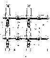
如图2所示,在TFT阵列基板10上,矩阵形地设置多个矩形的像素电极9(通过虚线部分9A示出轮廓),在像素电极9的纵横边界上,沿着各个边界设置数据线6a、扫描线3a以及电容线3b。在本实施形态中,各像素电极9以及把各像素电极9包围起来那样设置的数据线6a、扫描线3a、电容线3b等形成的区域的内侧是一个点区域,成为在每个矩阵形地配置的多个点区域中能够进行显示的构造。As shown in Figure 2, on the
数据线6a在构成TFT30的例如由多晶硅膜构成的半导体层1a中,经过连接孔5电连接到后述的源极区,像素电极9在半导体层1a中,经过连接孔8电连接到后述的漏极区。另外,在半导体层1a中,使得与沟道区(图中向左上方倾斜域的斜线区)相对那样配置扫描线3a,扫描线3a是与沟道区相对的部分,起到栅极电极的作用。The
电容线3b具有沿着扫描线3a大致直线形地延伸的主线部分(即,平面观看,沿着扫描线3a形成的第1区域),以及从与数据线6a交叉的位置沿着数据线6a突出到前方一侧(图中的上方向)的突出部分(即,平面观看,沿着数据线6a延伸的第2区域)。而且,图2中,在用向右上方倾斜的斜线所示的区域中,设置多个第1遮光膜11a。
另外,在一个点区域内,形成具备2个开口部分20a、20a的反射膜20,形成该反射膜20的区域成为反射显示区R,其内侧的没有形成反射膜20的区域(开口部分20a的内侧)成为透射显示区T1、T2。另外,形成矩形框形的绝缘膜21(液晶层厚调整层)使得当平面观察时在内部包括反射膜20的形成区域。在本实施形态的情况下,绝缘膜21具有倾斜面21a(参照图3),在本说明书中,把该部分定义为反射显示区R与透射显示区T1、T2的边界区域。In addition, in one dot region, a
其次,根据图3说明本实施形态的液晶显示装置的剖面构造。图3是沿着图2的A-A’线的剖面图,而本发明在绝缘膜或者电极的结构等方面具有特征,由于TFT或者其它部件的剖面构造与以往没有改变,因此省略TFT或者布线部分的图示以及说明。Next, the cross-sectional structure of the liquid crystal display device of this embodiment will be described with reference to FIG. 3 . Fig. 3 is a sectional view along the line AA' of Fig. 2, and the present invention is characterized in the structure of the insulating film or the electrode, etc., since the sectional structure of the TFT or other parts has not changed from the past, the TFT or the wiring are omitted. Some illustrations and descriptions.
如图3所示,本实施形态的液晶显示装置把由初始取向状态呈现垂直取向的介电各向异性为负的液晶构成的液晶层50夹在TFT阵列基板10和与其相对配置的对向基板25之间。TFT阵列基板10在由石英、玻璃等透光性材料构成的基板主体10A的表面上形成由铝、银等反射率高的金属膜构成的反射膜20。如上所述,反射膜20的形成区域成为反射显示区R,反射膜20的非形成区域成为透射显示区T1、T2。As shown in FIG. 3 , in the liquid crystal display device of this embodiment, a
在位于反射显示区R内的反射膜20上,以及在位于透射显示区T1、T2内的基板主体10A上,设置构成滤色片的色素层22。该色素层22在每个相邻的点区域中,配置红(R),绿(G),蓝(B)的不同颜色的色素层,由邻接的3个点区域构成1个像素。或者,也可以单独在反射显示区R和透射显示区T1(T2)中设置要在反射显示和透射显示中补偿显示色的色度不同的改变了色纯度的色素层。On the
在滤色片的色素层22上,在与反射显示区R相对应的位置上形成绝缘膜21。绝缘膜21例如由膜厚2μm±1μm左右的丙烯酸树脂等有机膜构成,在反射显示区R与透射显示区T1(T2)的边界附近,具有自身的膜厚连续变化的倾斜面21a。这里,由于不存在绝缘膜21的部分的液晶层50的厚度是2μm~6μm左右,因此反射显示区R中的液晶层50的厚度成为透射显示区T1(T2)中的液晶层50厚度的大约一半。即,绝缘膜21起到根据自身的膜厚使反射显示区R与透射显示区T1(T2)的液晶层50的厚度不同的液晶层厚调整层的作用。在本实施形态的情况下,绝缘膜21上部的平坦面的边缘与反射膜20(反射显示区)的边缘大致一致,在透射显示区T中包含倾斜面21a。On the
而且,在包含绝缘膜21的表面的TFT阵列基板10的表面上,形成由铟锡氧化物(Indium Tin Oxide,以下,简写为ITO)等的透明导电膜构成的像素电极9。另外,在像素电极9上形成由聚酰亚胺等构成的取向膜(省略图示)。Further, on the surface of the
另一方面,在对向基板25一侧,在由玻璃或者石英等透光性材料构成的基板主体25A上,顺序形成由ITO等透明导电膜构成的共用电极31,由聚酰亚胺等构成的取向膜(省略图示)。在TFT阵列基板10和对向基板25双方的取向膜(省略图示)上,同时实施垂直取向处理,但不实施摩擦等提供预倾斜的处理。On the other hand, on the
另外,在TFT阵列基板10的外侧面一侧以及对向基板25的外侧面一侧分别从基板主体一侧设置相位差板43、41,偏振板44、42。相位差板43、41具有对于可见光的波长大致1/4波长的相位差,通过该相位差板43、41与偏置光板44、42的组合,从TFT阵列基板10一侧以及对向基板25一侧向液晶层50入射大致圆偏振光。另外,在TFT阵列基板10外侧面一侧的液晶单元的外侧,设置具有光源61,反射器62,导光板63等的背光源64。In addition,
这里,在本实施形态的液晶显示装置中,为了取向限制液晶层50的液晶分子,在像素电极9以及共用电极31的预定位置设置缝隙。具体地讲,在像素电极9中,在透射显示区T1中的与绝缘膜21的倾斜面21a相对应的区域D中形成缝隙,另外,在透射显示区T2的中央部分附近B中也形成缝隙。另一方面,在共用电极31中,在透射显示区T1的中央部分附近C中形成缝隙,另外在透射显示区T2中的与绝缘膜21的倾斜面21a相对应的区域(位于倾斜面21a上方的区域)A中形成缝隙。从而,根据透射显示区T1、T2中心附近配置的缝隙的作用,液晶分子从透射显示区的内方朝向外方,以缝隙为基准,例如放射形地倾斜。Here, in the liquid crystal display device of the present embodiment, slits are provided at predetermined positions of the
如果依据这样的液晶显示装置,则通过在反射显示区R中设置绝缘膜21,能够把反射显示区R的液晶层50的厚度减小到透射显示区T的液晶层50厚度的大致一半,因此能够使在反射显示中起作用的延迟与在透射显示中起作用的延迟大致相等,由此能够谋求提高对比度。According to such a liquid crystal display device, by providing the insulating
进而,由于在一个像素内形成多个透射显示区,因此能够得到充分的透射率。而且,在这样形成了多个透射显示区的情况下,对于在一个点区域内邻接的透射显示区T1、T2,如上述那样,在区域中央部分B、C以及倾斜面21a的对应部分A、D中,在各区域T1、T2的各个相互不同的基板一侧形成电极缝隙。从而,如图4所示,在一个点内的每个邻接的透射显示区T1、T2中,液晶分子50b的倾斜方向相反,例如以对向基板25为基准观察的情况下,在透射显示区T2中,朝向该区域的内方(中心方向)液晶分子直立地取向,在另一方的透射显示区T1中,朝向该区域的外方,液晶分子直立地取向。进而,在反射显示区中,液晶分子的取向方向被限制为单方向。即,由于对于电极形成缝隙,因此加到上下电极之间的电场倾斜地畸变,通过倾斜电场的作用,能够控制液晶分子的取向方向。而且,由于使在每一个区域T1、T2中形成缝隙的位置(区域中央部分以及倾斜面)与形成缝隙的电极(像素电极以及共用电极)的关系相互不同,因此在位于各区域T1、T2之间的反射显示区R中,能够把液晶分子的倾斜方向确定为单一方向。Furthermore, since a plurality of transmissive display regions are formed in one pixel, sufficient transmittance can be obtained. Furthermore, when a plurality of transmissive display areas are formed in this way, for the adjacent transmissive display areas T1 and T2 in one dot area, as described above, the central parts B and C of the areas and the corresponding parts A and A of the
从而,如果依据本实施形态的液晶显示装置,则由于抑制发生向错,可以得到由发生向错产生的余像或者从倾斜方向观察时的斑点、不均匀等少的高品质的显示。而且,通过该作用,能够实现没有光遗漏等显示不良的高对比度,宽视角(160°锥体下1∶10以上的对比度)的显示。Therefore, according to the liquid crystal display device of this embodiment, since the occurrence of disclination is suppressed, a high-quality display with less afterimage due to the occurrence of disclination or spots and unevenness when viewed from an oblique direction can be obtained. Furthermore, this function enables display with high contrast and wide viewing angle (contrast ratio of 1:10 or more in a 160° cone) without display defects such as light leakage.
第2实施形态Second Embodiment
以下,参照图5说明本发明的第2实施形态。Next, a second embodiment of the present invention will be described with reference to FIG. 5 .
图5是示出本实施形态的液晶显示装置的剖面图。本实施形态的液晶显示装置的基本结构由于与第1实施形态大致相同,因此在图5中与图3相同的构成元件上标注相同的符号,并节省详细的说明。FIG. 5 is a cross-sectional view showing the liquid crystal display device of the present embodiment. Since the basic structure of the liquid crystal display device of this embodiment is substantially the same as that of the first embodiment, the same reference numerals are assigned to the same constituent elements in FIG. 5 as those in FIG. 3, and detailed descriptions are omitted.
本实施形态的情况下,如图5所示,在透射显示区T2的中央部分附近B的像素电极9上形成剖面为三角形的凸起,另外,在透射显示区T1的中央部分附近C的共用电极31上也形成剖面为三角形的凸起。该凸起例如用丙烯酸树脂等电介质材料形成,其平面形状形成为与第1实施形态的缝隙的平面形状大致相同。另外,形成取向膜(省略图示)使得覆盖各电极9、31以及凸起。另一方面,在作为透射显示区T1中的与倾斜面21a相对应的区域D中与第1实施形态相同,在像素电极9上形成缝隙,另外,在透射显示区T2中的倾斜面21a的上方区域A中,与第1实施形态相同,在共用电极31上形成缝隙。In the case of this embodiment, as shown in FIG. 5 , on the
如果依据本实施形态的液晶显示装置,则虽然在区域B、C中,与第1实施形态的缝隙不同,在液晶层50中形成突出的凸起,但是这种情况下也如图6所示,沿着该凸起的斜面取向控制液晶分子50b。即,在本实施形态的情况下,与第1实施形态同样地控制液晶分子50b的取向方向,由此,能够实现没有光遗漏等显示不良的高对比度、宽视角的显示。According to the liquid crystal display device of this embodiment, although in regions B and C, unlike the slits of the first embodiment, protruding protrusions are formed in the
以上,示出了本发明的第1实施形态以及第2实施形态,而在图3所示的区域A、C中,即使是在共用电极31上形成了缝隙或者形成了凸起的任一种情况下,也能够沿着相同的方向取向限制液晶分子50b(参照图4或者图6)。另外,在图3所示的区域B中,即使在像素电极9上形成了缝隙或者形成了凸起的任一种情况下,也能够沿着相同的方向取向限制液晶分子50b(参照图4或者图6)。另外,在图3所示的区域D中,由于难以在倾斜面上形成凸起,因此在像素电极9上形成缝隙。The above described the first embodiment and the second embodiment of the present invention, but in the regions A and C shown in FIG. Even in this case, the
这样,在图3所示的区域A、B、C中,即使对于电极形成缝隙或者凸起的某一个,也能够实现上述的防止光遗漏,提高对比度,展宽视角等的效果。即,如图7所示,根据对于区域A、B、C的缝隙或者凸起的选择,能够实现本发明的实施例1~实施例8的液晶显示装置,在任一种情况下都发现了与上述各实施形态相同的效果。另外,上述第1实施形态与图7中的实施例1相当,第2实施形态与实施例4相当。In this way, in the regions A, B, and C shown in FIG. 3 , even if any one of slits or protrusions is formed on the electrodes, the above-mentioned effects of preventing light leakage, improving contrast, and widening the viewing angle can be realized. That is, as shown in FIG. 7, according to the selection of the slits or protrusions in the regions A, B, and C, the liquid crystal display devices of Embodiment 1 to
另外,在上述第1实施形态以及第2实施形态中,示出了在一个像素电极9内适当地取向限制液晶分子的结构,而由于在邻接的像素电极9、9之间形成间隙(电极非形成部分),因此作为共用电极31如果使用整个面形状的电极,则在该像素电极9的非形成部分中,在与共用电极31之间将产生倾斜电场。In addition, in the first embodiment and the second embodiment described above, the structure in which the liquid crystal molecules are appropriately regulated in one
特别是,在图4所示的反射显示区R中,如果沿着与液晶分子的倾斜方向交叉的方向产生影响到取向限制力的倾斜电场,则恐怕不能够适宜地实现作为本实施形态目的的取向限制,即,在反射显示区中把液晶分子的取向方向取向限制为单一方向。In particular, in the reflective display region R shown in FIG. 4, if an oblique electric field that affects the orientation-regulating force is generated along a direction intersecting with the inclination direction of the liquid crystal molecules, it may not be possible to properly realize the purpose of this embodiment. Orientation restriction, that is, restricting the alignment direction of liquid crystal molecules to a single direction in the reflective display area.
因此,在第1实施形态以及第2实施形态的每一个中,在平面地重叠在形成于反射显示区R中的像素电极9、9之间的间隙(电极非形成部分)的位置,在共用电极31上设置缝隙(开口部分)。具体地讲,形成图9所示形状的电极缝隙。Therefore, in each of the first embodiment and the second embodiment, at the position superimposed planarly on the gap (electrode non-formation portion) between the
图9(a)是像素电极9的平面模式图,图9(b)是共用电极31的平面模式图。另外,在图9(b)中用虚线示出平面地重叠在共用电极31上的像素电极9。另外,在各实施形态的反射显示区R中,沿着图9所示的像素电极9的长度方向取向限制液晶分子。9( a ) is a schematic plan view of the
如图9(b)所示,在上述各实施形态的共用电极31中部分地形成缝隙(开口部分)31a。该缝隙31a形成在反射显示区R中,而且,以平面地重叠到像素电极9、9之间的间隙(电极非形成部分)的形状形成。As shown in FIG. 9( b ), a slit (opening portion) 31 a is partially formed in the
根据以上的结构,在反射显示区R中,难以发生由形成在像素电极9、9之间的间隙(电极非形成部分)引起的倾斜电场,难以产生扰乱取向限制的倾斜电场。从而,难以发生由于像素之间的间隙引起的倾斜电场,在与沿着图9(a)的像素电极9的长度方向的反射显示区R的液晶分子取向方向交叉的方向(图9(a)的像素电极9的宽度方向)影响取向限制力的不理想状况。According to the above configuration, in the reflective display region R, it is difficult to generate an oblique electric field due to the gap (electrode non-formation portion) formed between the
电子设备Electronic equipment
其次,说明具备了本发明上述实施形态的液晶显示装置的电子设备的具体例子。Next, a specific example of electronic equipment including the liquid crystal display device according to the above-mentioned embodiment of the present invention will be described.
图8是示出了便携电话一例的立体图。图8中,符号500示出便携电话主体,符号501示出使用了上述液晶显示装置的显示部。Fig. 8 is a perspective view showing an example of a mobile phone. In FIG. 8,
图8所示的电子设备由于具备使用了上述实施形态的液晶显示装置的显示部,因此与使用环境无关,能够实现具备明亮、对比度高、宽视角的液晶显示部的电子设备。另外,特别是在透射显示时由于能够得到明亮、高对比度的显示,因此能够提供重视透射显示的电子设备。Since the electronic equipment shown in FIG. 8 includes a display unit using the liquid crystal display device of the above-mentioned embodiment, it is possible to realize an electronic equipment equipped with a bright, high-contrast, wide-viewing-angle liquid crystal display unit regardless of the usage environment. In addition, since a bright and high-contrast display can be obtained particularly in the case of a transmissive display, it is possible to provide an electronic device that places emphasis on a transmissive display.
另外,本发明的技术范围不限于上述实施形态,在不脱离本发明宗旨的范围内能够加入各种变更。例如,在上述实施形态中示出了在把TFT作为开关元件的有源矩阵型液晶显示装置中适用了本发明的例子,而也能够在把薄膜二极管(Thin Film Diode,TFD)作为开关元件的有源矩阵型液晶显示装置、无源矩阵型液晶显示装置等中适用本发明。除此以外,关于各种构成元件的材料、尺寸、形状等的具体记述也能够进行适当变更。In addition, the technical scope of this invention is not limited to the said embodiment, Various changes can be added in the range which does not deviate from the summary of this invention. For example, in the above-mentioned embodiment, an example in which the present invention is applied to an active matrix type liquid crystal display device using TFT as a switching element is shown, but it can also be used in a thin film diode (Thin Film Diode, TFD) as a switching element. The present invention is applicable to active matrix liquid crystal display devices, passive matrix liquid crystal display devices, and the like. In addition, specific descriptions about materials, dimensions, shapes, etc. of various constituent elements can also be appropriately changed.
另外,在上述实施形态中,示出了用单板构成相位差板41、42,而代替单板,也可以构成为1/2波长板和1/4波长板的叠层体。该叠层体起到宽带圆偏振板的作用,能够使黑显示进一步无色彩。进而,通过在该叠层体上叠层负的C板,还能够谋求更大的视角。另外,所谓C板是在膜厚方向具有光轴的相位差板。In addition, in the above embodiment, the
进而,在上述实施形态中,作为液晶层厚调整层把绝缘膜21形成在TFT阵列基板10一侧的基板主体(下基板)10A上,而也能够形成在对向基板25一侧的基板主体(上基板)25A上。另外,对于滤色片(着色层22)也相同,在上述实施形态中形成在TFT阵列基板10一侧的基板主体(下基板)10A上,而也能够形成在对向基板25一侧的基板主体(上基板)25A上。Furthermore, in the above-mentioned embodiment, the insulating
Claims (4)
Translated fromChineseApplications Claiming Priority (4)
| Application Number | Priority Date | Filing Date | Title |
|---|---|---|---|
| JP2003068338 | 2003-03-13 | ||
| JP068338/2003 | 2003-03-13 | ||
| JP2003382827AJP3900141B2 (en) | 2003-03-13 | 2003-11-12 | Liquid crystal display device and electronic device |
| JP382827/2003 | 2003-11-12 |
Publications (2)
| Publication Number | Publication Date |
|---|---|
| CN1530697Atrue CN1530697A (en) | 2004-09-22 |
| CN1303461C CN1303461C (en) | 2007-03-07 |
Family
ID=33302174
Family Applications (1)
| Application Number | Title | Priority Date | Filing Date |
|---|---|---|---|
| CNB2004100064476AExpired - LifetimeCN1303461C (en) | 2003-03-13 | 2004-03-08 | Liquid-crystal displaying device and electronic apparatus |
Country Status (5)
| Country | Link |
|---|---|
| US (1) | US7046322B2 (en) |
| JP (1) | JP3900141B2 (en) |
| KR (1) | KR100579346B1 (en) |
| CN (1) | CN1303461C (en) |
| TW (1) | TWI266919B (en) |
Cited By (3)
| Publication number | Priority date | Publication date | Assignee | Title |
|---|---|---|---|---|
| CN100485493C (en)* | 2005-07-15 | 2009-05-06 | 爱普生映像元器件有限公司 | Liquid crystal display device and electronic apparatus |
| CN102308251A (en)* | 2009-02-09 | 2012-01-04 | 夏普株式会社 | Liquid crystal display device |
| CN107315288A (en)* | 2017-08-17 | 2017-11-03 | 京东方科技集团股份有限公司 | A kind of array base palte, liquid crystal panel and its manufacture craft |
Families Citing this family (18)
| Publication number | Priority date | Publication date | Assignee | Title |
|---|---|---|---|---|
| TW594310B (en)* | 2003-05-12 | 2004-06-21 | Hannstar Display Corp | Transflective LCD with single cell gap and the fabrication method thereof |
| JP2005292515A (en)* | 2004-03-31 | 2005-10-20 | Sharp Corp | Liquid crystal display device, driving method thereof, and electronic apparatus |
| KR20060034802A (en)* | 2004-10-19 | 2006-04-26 | 삼성전자주식회사 | Transflective Liquid Crystal Display |
| JP4662947B2 (en)* | 2004-11-05 | 2011-03-30 | シャープ株式会社 | Liquid crystal display device and electronic apparatus including the same |
| US7411636B2 (en)* | 2004-11-23 | 2008-08-12 | Fergason Patent Properties, Llc | Stereoscopic liquid crystal display (LCD) with polarization method |
| US20060158587A1 (en)* | 2005-01-20 | 2006-07-20 | Au Optronics Corporation | Transflective liquid crystal display |
| TW200634372A (en)* | 2005-03-22 | 2006-10-01 | Wintek Corp | Transflective liquid crystal display device |
| US7924382B2 (en)* | 2005-05-25 | 2011-04-12 | Sharp Kabushiki Kaisha | Liquid crystal display device substrate, method of manufacturing liquid crystal display device substrate, liquid crystal display device and method of manufacturing liquid crystal display device |
| JP2007058045A (en)* | 2005-08-26 | 2007-03-08 | Toshiba Matsushita Display Technology Co Ltd | Liquid crystal display apparatus |
| US7821613B2 (en) | 2005-12-28 | 2010-10-26 | Semiconductor Energy Laboratory Co., Ltd. | Display device and manufacturing method thereof |
| TW200742895A (en)* | 2006-05-12 | 2007-11-16 | Innolux Display Corp | Transflective liquid crystal display device |
| TWI303487B (en)* | 2006-06-13 | 2008-11-21 | Au Optronics Corp | Method for manufactruring an array substate of a transflective liquid crystal display |
| US7782427B2 (en)* | 2006-06-30 | 2010-08-24 | Lg Display Co., Ltd. | Transflective type liquid crystal display device |
| TW200817767A (en)* | 2006-10-12 | 2008-04-16 | Wintek Corp | Transflective multi-domain liquid crystal display device |
| TWI349154B (en)* | 2006-10-19 | 2011-09-21 | Wintek Corp | Liquid crystal display panel and liquid crystal display device incorporating the same |
| CN101689000B (en)* | 2007-06-27 | 2012-07-18 | 夏普株式会社 | Liquid crystal display device |
| JP2009258332A (en)* | 2008-04-16 | 2009-11-05 | Seiko Epson Corp | Liquid crystal display device and electronic device |
| JP2015090436A (en)* | 2013-11-06 | 2015-05-11 | 株式会社ジャパンディスプレイ | Liquid crystal display |
Family Cites Families (12)
| Publication number | Priority date | Publication date | Assignee | Title |
|---|---|---|---|---|
| TW509808B (en) | 1997-06-12 | 2002-11-11 | Sharp Kk | Liquid crystal display device |
| US6281952B1 (en)* | 1997-12-26 | 2001-08-28 | Sharp Kabushiki Kaisha | Liquid crystal display |
| KR100309918B1 (en)* | 1998-05-16 | 2001-12-17 | 윤종용 | Liquid crystal display having wide viewing angle and method for manufacturing the same |
| JP3610264B2 (en) | 1999-08-03 | 2005-01-12 | シャープ株式会社 | Liquid crystal display element |
| KR100312328B1 (en)* | 1999-08-06 | 2001-11-03 | 구본준, 론 위라하디락사 | Transflective liquid crystal display device |
| JP3744342B2 (en)* | 1999-12-03 | 2006-02-08 | セイコーエプソン株式会社 | Liquid crystal device and electronic device |
| JP3600531B2 (en) | 2000-02-25 | 2004-12-15 | シャープ株式会社 | Liquid crystal display |
| KR20020012794A (en)* | 2000-08-08 | 2002-02-20 | 구본준, 론 위라하디락사 | a method for fabricating transflective liquid crystal display device and the same |
| JP2002287158A (en) | 2000-12-15 | 2002-10-03 | Nec Corp | Liquid crystal display device and method of manufacturing the same as well as driving method for the same |
| JP3875125B2 (en)* | 2001-04-11 | 2007-01-31 | シャープ株式会社 | Liquid crystal display |
| JP3767419B2 (en) | 2001-05-28 | 2006-04-19 | ソニー株式会社 | Liquid crystal display element |
| JP3490995B2 (en)* | 2001-12-28 | 2004-01-26 | シャープ株式会社 | Active matrix type liquid crystal display |
- 2003
- 2003-11-12JPJP2003382827Apatent/JP3900141B2/ennot_activeExpired - Lifetime
- 2004
- 2004-02-17USUS10/778,020patent/US7046322B2/ennot_activeExpired - Lifetime
- 2004-03-03TWTW093105582Apatent/TWI266919B/ennot_activeIP Right Cessation
- 2004-03-08CNCNB2004100064476Apatent/CN1303461C/ennot_activeExpired - Lifetime
- 2004-03-12KRKR1020040016990Apatent/KR100579346B1/ennot_activeExpired - Lifetime
Cited By (4)
| Publication number | Priority date | Publication date | Assignee | Title |
|---|---|---|---|---|
| CN100485493C (en)* | 2005-07-15 | 2009-05-06 | 爱普生映像元器件有限公司 | Liquid crystal display device and electronic apparatus |
| CN102308251A (en)* | 2009-02-09 | 2012-01-04 | 夏普株式会社 | Liquid crystal display device |
| US8654049B2 (en) | 2009-02-09 | 2014-02-18 | Sharp Kabushiki Kaisha | Liquid crystal display device |
| CN107315288A (en)* | 2017-08-17 | 2017-11-03 | 京东方科技集团股份有限公司 | A kind of array base palte, liquid crystal panel and its manufacture craft |
Also Published As
| Publication number | Publication date |
|---|---|
| KR100579346B1 (en) | 2006-05-12 |
| US20040212763A1 (en) | 2004-10-28 |
| CN1303461C (en) | 2007-03-07 |
| US7046322B2 (en) | 2006-05-16 |
| KR20040081387A (en) | 2004-09-21 |
| JP2004295077A (en) | 2004-10-21 |
| TWI266919B (en) | 2006-11-21 |
| JP3900141B2 (en) | 2007-04-04 |
| TW200424617A (en) | 2004-11-16 |
Similar Documents
| Publication | Publication Date | Title |
|---|---|---|
| CN1301438C (en) | Liquid-crystal displaying device and electronic apparatus | |
| CN100478767C (en) | Liquid crystal display device and electronic device | |
| TWI224699B (en) | Liquid crystal display and electronic device | |
| CN1293416C (en) | Liquid-crystal displaying device and electronic apparatus | |
| US7576818B2 (en) | Liquid crystal display device and electronic apparatus | |
| CN100428011C (en) | Liquid crystal display device and electronic equipment | |
| CN1530697A (en) | Liquid crystal display device and electronic equipment | |
| CN1661421A (en) | Viewing angle control element and manufacturing method thereof, liquid crystal display device, electronic device | |
| CN100485503C (en) | Liquid crystal display plate | |
| CN1743922A (en) | Liquid crystal display device, electronic equipment | |
| CN1746751A (en) | Liquid crystal display device and electronic equipment | |
| CN1282005C (en) | Liquid crystal display device and electronic equipment | |
| JP2007206342A (en) | Liquid crystal and electronic device | |
| JP2004198919A (en) | Liquid crystal display and electronic equipment | |
| CN1641424A (en) | Liquid crystal display device and electronic apparatus | |
| JP3901172B2 (en) | Liquid crystal display device and electronic device | |
| CN1519616A (en) | Liquid crystal display device and electronic equipment | |
| CN100345050C (en) | Liquid crystal device and electronic equipment | |
| WO2010038507A1 (en) | Liquid crystal display device | |
| JP2007140089A (en) | Liquid crystal display | |
| JP2005055595A (en) | Liquid crystal display device, driving method thereof, and electronic apparatus | |
| JP4196672B2 (en) | Liquid crystal display device and electronic device | |
| CN1282014C (en) | Liquid crystal display device and electronic equipment | |
| JP4325190B2 (en) | Liquid crystal display device and electronic device | |
| JP2004198922A (en) | Liquid crystal display and electronic equipment |
Legal Events
| Date | Code | Title | Description |
|---|---|---|---|
| C06 | Publication | ||
| PB01 | Publication | ||
| C10 | Entry into substantive examination | ||
| SE01 | Entry into force of request for substantive examination | ||
| C14 | Grant of patent or utility model | ||
| GR01 | Patent grant | ||
| C41 | Transfer of patent application or patent right or utility model | ||
| TR01 | Transfer of patent right | Effective date of registration:20160530 Address after:100015 Jiuxianqiao Road, Beijing, No. 10, No. Patentee after:BOE TECHNOLOGY GROUP Co.,Ltd. Address before:Hongkong, China Patentee before:BOE Technology (Hongkong) Co.,Ltd. Effective date of registration:20160530 Address after:Hongkong, China Patentee after:BOE Technology (Hongkong) Co.,Ltd. Address before:Tokyo, Japan Patentee before:Seiko Epson Corp. | |
| CX01 | Expiry of patent term | Granted publication date:20070307 | |
| CX01 | Expiry of patent term |