CN1529947A - receivers and communication terminals - Google Patents
receivers and communication terminalsDownload PDFInfo
- Publication number
- CN1529947A CN1529947ACNA028143248ACN02814324ACN1529947ACN 1529947 ACN1529947 ACN 1529947ACN A028143248 ACNA028143248 ACN A028143248ACN 02814324 ACN02814324 ACN 02814324ACN 1529947 ACN1529947 ACN 1529947A
- Authority
- CN
- China
- Prior art keywords
- section
- signal
- receiver
- frequency
- quadrature mixer
- Prior art date
- Legal status (The legal status is an assumption and is not a legal conclusion. Google has not performed a legal analysis and makes no representation as to the accuracy of the status listed.)
- Pending
Links
Images


Classifications
- H—ELECTRICITY
- H04—ELECTRIC COMMUNICATION TECHNIQUE
- H04B—TRANSMISSION
- H04B1/00—Details of transmission systems, not covered by a single one of groups H04B3/00 - H04B13/00; Details of transmission systems not characterised by the medium used for transmission
- H04B1/005—Details of transmission systems, not covered by a single one of groups H04B3/00 - H04B13/00; Details of transmission systems not characterised by the medium used for transmission adapting radio receivers, transmitters andtransceivers for operation on two or more bands, i.e. frequency ranges
- H04B1/0053—Details of transmission systems, not covered by a single one of groups H04B3/00 - H04B13/00; Details of transmission systems not characterised by the medium used for transmission adapting radio receivers, transmitters andtransceivers for operation on two or more bands, i.e. frequency ranges with common antenna for more than one band
- H04B1/0057—Details of transmission systems, not covered by a single one of groups H04B3/00 - H04B13/00; Details of transmission systems not characterised by the medium used for transmission adapting radio receivers, transmitters andtransceivers for operation on two or more bands, i.e. frequency ranges with common antenna for more than one band using diplexing or multiplexing filters for selecting the desired band
- H—ELECTRICITY
- H04—ELECTRIC COMMUNICATION TECHNIQUE
- H04B—TRANSMISSION
- H04B1/00—Details of transmission systems, not covered by a single one of groups H04B3/00 - H04B13/00; Details of transmission systems not characterised by the medium used for transmission
- H04B1/005—Details of transmission systems, not covered by a single one of groups H04B3/00 - H04B13/00; Details of transmission systems not characterised by the medium used for transmission adapting radio receivers, transmitters andtransceivers for operation on two or more bands, i.e. frequency ranges
- H04B1/0053—Details of transmission systems, not covered by a single one of groups H04B3/00 - H04B13/00; Details of transmission systems not characterised by the medium used for transmission adapting radio receivers, transmitters andtransceivers for operation on two or more bands, i.e. frequency ranges with common antenna for more than one band
- H04B1/006—Details of transmission systems, not covered by a single one of groups H04B3/00 - H04B13/00; Details of transmission systems not characterised by the medium used for transmission adapting radio receivers, transmitters andtransceivers for operation on two or more bands, i.e. frequency ranges with common antenna for more than one band using switches for selecting the desired band
- H—ELECTRICITY
- H04—ELECTRIC COMMUNICATION TECHNIQUE
- H04B—TRANSMISSION
- H04B1/00—Details of transmission systems, not covered by a single one of groups H04B3/00 - H04B13/00; Details of transmission systems not characterised by the medium used for transmission
- H04B1/38—Transceivers, i.e. devices in which transmitter and receiver form a structural unit and in which at least one part is used for functions of transmitting and receiving
- H04B1/40—Circuits
- H04B1/403—Circuits using the same oscillator for generating both the transmitter frequency and the receiver local oscillator frequency
- H04B1/406—Circuits using the same oscillator for generating both the transmitter frequency and the receiver local oscillator frequency with more than one transmission mode, e.g. analog and digital modes
Landscapes
- Engineering & Computer Science (AREA)
- Computer Networks & Wireless Communication (AREA)
- Signal Processing (AREA)
- Superheterodyne Receivers (AREA)
- Circuits Of Receivers In General (AREA)
- Digital Transmission Methods That Use Modulated Carrier Waves (AREA)
- Noise Elimination (AREA)
Abstract
Description
Translated fromChinese技术领域technical field
本发明涉及一种适合于多种通信系统的多模式接收机和通信终端。The invention relates to a multi-mode receiver and communication terminal suitable for various communication systems.
背景技术Background technique
近年来,零IF接收机(以下称作“ZIF接收机”)和低IF接收机(以下称作“LIF接收机”)正在顺利发展,低IF接收机中超外差式接收机的中频被设置成非常低的频率。在ZIF接收机和LIF接收机中,因为由例如SAW滤波器、陶瓷滤波器等分立元件组成的信道选择滤波器被构造在IC芯片上,所以可以实现嵌入简单、终端小型化以及低成本。In recent years, zero-IF receivers (hereinafter referred to as "ZIF receivers") and low-IF receivers (hereinafter referred to as "LIF receivers") are developing smoothly, and the intermediate frequency of superheterodyne receivers in low-IF receivers is set into very low frequencies. In ZIF receivers and LIF receivers, since channel selection filters composed of discrete components such as SAW filters, ceramic filters, etc. are constructed on IC chips, simplicity of embedding, miniaturization of terminals, and low cost can be achieved.
同样,近年来,需要一种能够通过相同终端在不同通信系统之间例如PDC和PHS、IS95和AMPS之间发送/接收信号的多模式接收机。以下将说明现有技术中的多模式类型接收机。在TDMA系统的无线电系统中,例如GSM和PDC、PHS等,通常断续操作接收机以减少消耗电流。相反,在例如W-CDMA、IS95等的CDMA系统的无线电系统中,或例如AMPS等的模拟系统中,接收机在通信期间执行持续的接收操作。Also, in recent years, a multi-mode receiver capable of transmitting/receiving signals between different communication systems such as PDC and PHS, IS95 and AMPS through the same terminal is required. A multi-mode type receiver in the prior art will be described below. In radio systems of TDMA systems, such as GSM and PDC, PHS, etc., receivers are usually operated intermittently to reduce consumption current. In contrast, in a radio system of a CDMA system such as W-CDMA, IS95, etc., or an analog system such as AMPS, etc., a receiver performs a continuous receiving operation during communication.
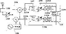
首先,以下将参照图23说明现有技术中的ZIF接收机。通过天线101接收的无线电信号除接收频带外被高频滤波器102衰减,然后被高频放大器103放大。通过利用正交混频器104对本机振荡器部分105的输出信号与被高频放大器103放大的信号进行混频,来产生具有正交关系的基带I信号和Q信号,其中本机振荡器部分105输出一对具有几乎与接收频率相同的频率的正交本机振荡信号。接着,通过利用信道选择滤波器107a、107b限制I、Q信号的带宽来去除不需要的波,然后利用可变增益放大器108a、108b将I、Q信号放大到所需电平,然后利用解码部分110对其进行解码。First, a ZIF receiver in the prior art will be described below with reference to FIG. 23 . A radio signal received through the
在该ZIF接收机中,基带的偏移电压使接收灵敏度恶化。由于电路组成元件之间的不匹配,以及正交混频器104在本机振荡器部分105的输出和泄漏到正交混频器104的高频信号输入端的本机振荡信号之间的自混频,因而产生偏移电压。在图23所示的ZIF接收机中,通过在各电路部分之间提供HPF(高通滤波器)来消除基带中产生的偏移电压,其中HPF由第一耦合电容器106、第二耦合电容器109等组成。In this ZIF receiver, the offset voltage of the baseband deteriorates the reception sensitivity. Due to the mismatch between the circuit constituent elements and the self-mixing of the
在TDMA系统中,由于执行只接收有关时隙的断续接收操作,必须使接收机高速启动并且迅速转变到接收操作。但是,如果采用电容耦合来消除偏移电压,如图24所示,启动时,在HPF的截止频率中就会产生DC偏压变化121。因此,直到接收机稳定时所需的偏压稳定时间122的时间常数极大地延长了启动时间。同样,由于I、Q信号的低频分量被衰减,或者群延迟时间被HPF改变,就有可能使接收特性恶化。In the TDMA system, since a discontinuous receiving operation is performed in which only relevant time slots are received, it is necessary for the receiver to start up at high speed and transition to the receiving operation quickly. However, if capacitive coupling is used to cancel the offset voltage, as shown in Figure 24, a DC
在JP-A-7-111471中也阐述了用于消除偏移电压的装置。图25示出该公布中所阐述的偏移电压消除电路的概况。在这种情况下,由于接收机的基本结构与图23所示的相似,这里将省略对它们的说明。在图25中,利用包含在解码部分110中的ADC (AD变换器)110a、110b和偏移电压检测部分110c来检测I、Q分量中的偏移电压,然后通过向加法器111a、111b、110d、110e提供负反馈来消除偏移电压。利用这种结构,特别需要偏移电压消除电路,但是因为必须将偏移电压调整到对弱接收信号振幅足够小的值,所以很难简单地实现这种电路。同样,由于除正常接收操作之外,还需要多次检测/校正偏移电压,接收机的工作时间被延长,于是电池工作时间被缩短。A means for canceling the offset voltage is also described in JP-A-7-111471. FIG. 25 shows an overview of the offset voltage canceling circuit set forth in this publication. In this case, since the basic structure of the receiver is similar to that shown in Fig. 23, their description will be omitted here. In FIG. 25, utilize ADC (AD converter) 110a, 110b and offset
接下来,将参照图26说明现有技术中的LIF接收机。在图26中,将相同的标号附加到与图24(现有技术中的ZIF接收机)中那些部分完全相同的部分。通过天线101接收的无线电信号除接收频带外被高频滤波器102衰减,并且被高频放大器103放大。接着,通过利用正交混频器104对本机振荡器部分105的输出信号与被高频放大器103放大的信号进行混频,将信号变换成具有正交关系的I、Q分量的中频(IF)信号,其中,本机振荡器部分105输出一对其频率被从无线电信号偏移的正交本机振荡信号。接着,通过利用信道选择滤波器107a、107b限制I、Q信号的带宽,去除不需要的波,并且由可变增益放大器108a、108b将I、Q信号放大到所需电平。Next, a LIF receiver in the prior art will be explained with reference to FIG. 26 . In FIG. 26, the same reference numerals are attached to the parts identical to those in FIG. 24 (ZIF receiver in prior art). A radio signal received through the
在该LIF接收机中,由于信号的频率被变换到低中频,能够利用由电容耦合构成的HPF,来消除信道选择滤波器107a、107b和可变增益放大器108a、108b中产生的偏移电压。换句话说,可以由BPF(带通滤波器)构造信道选择滤波器107a、107b。接着,通过利用第二正交混频器112对第二本机振荡器部分113的输出信号与IF信号进行混频,来产生相互具有正交关系的基带I信号和Q信号,其中,第二本机振荡器部分113输出一对具有几乎与中频相同的频率的正交本机振荡信号。图26所示的LIF接收机是Weber类型的镜像消除混频器,镜像信号被第二正交混频器112消除,以及由第二信道选择滤波器114a、114b去除不需要的波,然后该信号被解码部分110解码。In this LIF receiver, since the frequency of the signal is converted to a low intermediate frequency, the offset voltage generated in the channel selection filters 107a, 107b and the variable gain amplifiers 108a, 108b can be eliminated by using the HPF constituted by capacitive coupling. In other words, the channel selection filters 107a, 107b can be constructed by BPF (Band Pass Filter). Next, by mixing the output signal of the second
图27示出上述现有技术中的LIF接收机中的一组中频示例。符号131表示高频带中信号的排列,符号133表示中频带中信号的排列。在相邻信号波131b、131c、131d、131e、131f充当所期望的接收波131a的干扰波的情况下,如果以此方式设置第一本机振荡频率132,使图26所示的第一本机振荡器部分105的输出频率具有1/2信道间隔,那么所期望的接收波133a和相邻信号波133b、133c、133d、133e、133f就被排列在中频带133中。在这种情况下,相邻信号波133c给出镜像信号。Fig. 27 shows an example of a set of intermediate frequencies in the LIF receiver in the prior art described above.
在使用中频的接收系统中,总是出现镜像信号,这是众所周知的。在使用TDMA系统的蜂窝式电话的情况下,用于例如PDC、PHS中的频率被计划,以便使充当干扰的相邻信号波被分离超过下一个相邻信道频率。同样,由于在GSM中使用相邻信道频率,但放宽了抗干扰的标准,所以应该将1/2信道间隔的频率用作中频,如图27所示。更具体地,在PDC中采用IF=12.5kHz,在PHS中采用IF=150kHz,在GSM中采用IF=100kHz。In receiving systems using intermediate frequencies, image signals always appear, which is well known. In the case of a cellular phone using a TDMA system, frequencies used in eg PDC, PHS are planned so that adjacent signal waves acting as interference are separated beyond the next adjacent channel frequency. Also, since the adjacent channel frequency is used in GSM, but the anti-interference standard is relaxed, the frequency of 1/2 channel spacing should be used as the intermediate frequency, as shown in Figure 27. More specifically, IF=12.5 kHz is used in PDC, IF=150 kHz is used in PHS, and IF=100 kHz is used in GSM.
因此,通过使用镜像消除混频器来抑制相应于镜像频率的相邻信道带宽中的信号。如上所述,在使用TDMA系统的蜂窝式电话中,不使用相邻信道频率,或者放宽了抗干扰的标准。于是,由于镜像消除混频器能够容易地将镜像信号消除到大约30dB的程度,所以可以确保足够的相邻信号波的抗干扰性能。相反,在CDMA系统中,使用相邻信道频率,于是仅镜像消除混频器需要抑制60dB或更多。通过I、Q之间相位的正交性和幅度的一致性来确定镜像消除量。为了得到60dB或更多的镜像消除特性,I、Q之间正交相位的误差必须被抑制在0.1度或更少,I、Q之间幅度误差也必须被抑制在0.1dB或更少。因此,很难实现这种镜像消除混频器。Therefore, signals in the adjacent channel bandwidth corresponding to the image frequency are suppressed by using an image cancel mixer. As described above, in a cellular phone using the TDMA system, adjacent channel frequencies are not used, or the anti-jamming standard is relaxed. Then, since the image cancel mixer can easily cancel the image signal to the extent of about 30 dB, sufficient anti-interference performance of adjacent signal waves can be ensured. In contrast, in a CDMA system, adjacent channel frequencies are used, so only the image cancellation mixer needs to reject 6OdB or more. The amount of image cancellation is determined by the orthogonality of the phase and the consistency of the amplitude between I and Q. In order to obtain image cancellation characteristics of 60dB or more, the quadrature phase error between I and Q must be suppressed at 0.1 degree or less, and the amplitude error between I and Q must also be suppressed at 0.1dB or less. Therefore, it is difficult to implement such an image canceling mixer.
如上所述,当构造适合于多种通信系统的多模式接收机时,会出现以下问题。首先,当ZIF接收机被用于TDMA系统例如GSM和PDC、PHS等时,接收机中各部分被电容耦合以便消除偏移电压。因此,问题在于很难高速启动终端。同样,问题还在于很难通过简单的电路结构实现调整功能。相反,当LIF接收机被用于CDMA系统例如IS-95、W-CDMA等时,问题在于很难简单地实现用于确保相邻信道干扰特性的镜像消除混频器。因此,当适合于TDMA系统和CDMA系统两者的接收机由ZIF接收机或LIF接收机中的任何一种组成时,问题都在于不能获得所期望的特性。As described above, when constructing a multi-mode receiver suitable for various communication systems, the following problems arise. First, when a ZIF receiver is used in a TDMA system such as GSM and PDC, PHS, etc., various parts in the receiver are capacitively coupled in order to eliminate the offset voltage. Therefore, the problem is that it is difficult to start the terminal at high speed. Also, the problem is that it is difficult to realize the adjustment function with a simple circuit structure. In contrast, when a LIF receiver is used in a CDMA system such as IS-95, W-CDMA, etc., there is a problem in that it is difficult to simply implement an image cancellation mixer for ensuring adjacent channel interference characteristics. Therefore, when a receiver suitable for both the TDMA system and the CDMA system is composed of either a ZIF receiver or a LIF receiver, there is a problem in that desired characteristics cannot be obtained.
鉴于上述问题,做出本发明。本发明的一个目的是提供一种适合于多种通信系统的接收机和通信终端。The present invention has been made in view of the above problems. An object of the present invention is to provide a receiver and a communication terminal suitable for various communication systems.
发明内容Contents of the invention
为了克服上述问题,根据本发明的接收机适合于TDMA系统和CDMA系统这两种通信系统,它包括:第一正交混频器部分,用于利用具有预定频率的信号对接收信号进行正交变换;解码部分,用于对经过正交变换的信号进行解码;改变开关部分,用于当通信系统是TDMA系统或CDMA系统时,将信号路径从第一正交混频器部分切换到解码部分;以及第二正交混频器部分,用于对在第一正交混频器部分中经过正交变换的信号进行正交变换;其中,当通信系统是TDMA系统时,第一正交混频器部分利用频率偏移接收信号的信号对接收信号进行正交变换,改变开关部分选择信号路径,通过该信号路径,在第一正交混频器部分中经过正交变换的信号经由第二正交混频器部分被输入到解码部分,以及当通信系统是CDMA系统时,第一正交混频器部分利用频率与接收信号相同的信号对接收信号进行正交变换,改变开关部分选择信号路径,通过该信号路径,在第一正交混频器部分中经过正交变换的信号被输入到解码部分,而没有第二正交混频器部分的介入。In order to overcome the above-mentioned problems, the receiver according to the present invention is suitable for both communication systems of the TDMA system and the CDMA system, and includes: a first quadrature mixer section for quadrature the received signal with a signal having a predetermined frequency transformation; a decoding part for decoding the signal through the orthogonal transformation; a change switch part for switching the signal path from the first quadrature mixer part to the decoding part when the communication system is a TDMA system or a CDMA system and a second quadrature mixer section for orthogonally transforming the signal that has been orthogonally transformed in the first quadrature mixer section; wherein, when the communication system is a TDMA system, the first quadrature mixer The frequency converter part utilizes the frequency shifted signal of the received signal to perform orthogonal transformation on the received signal, and the switch part is changed to select a signal path through which the signal that has been orthogonally transformed in the first quadrature mixer part passes through the second The quadrature mixer section is input to the decoding section, and when the communication system is a CDMA system, the first quadrature mixer section performs orthogonal transformation on the received signal with a signal having the same frequency as the received signal, changing the switch section selection signal path through which the signal subjected to the orthogonal transformation in the first quadrature mixer section is input to the decoding section without intervention of the second quadrature mixer section.
同样,在根据本发明的接收机中,解码部分具有用于解码TDMA系统信号的TDMA解码部分和用于解码CDMA系统信号的CDMA解码部分,当通信系统是TDMA系统时,使用TDMA解码部分对信号进行解码,以及当通信系统是CDMA系统时,使用CDMA解码部分对信号进行解码。Also, in the receiver according to the present invention, the decoding section has a TDMA decoding section for decoding a TDMA system signal and a CDMA decoding section for decoding a CDMA system signal, and when the communication system is a TDMA system, the signal is decoded using the TDMA decoding section. Decoding is performed, and when the communication system is a CDMA system, the signal is decoded using the CDMA decoding section.
同样,根据本发明的接收机还包括:第一滤波器部分,用于对在第一正交混频器部分中经过正交变换的信号进行频带限制;第二滤波器部分,用于对在第一滤波器部分中经过频带限制并且还在第一正交混频器部分或第二正交混频器部分中经过正交变换的信号进行频带限制;滤波器设置改变部分,用于根据通信系统,改变第一滤波器部分和第二滤波器部分的设置;高频放大器部分,用于放大接收信号;可变增益放大器部分,用于将在第一滤波器部分中经过频带限制的信号调整到预定幅度电平;和增益改变部分,用于根据输入到解码部分的信号的幅度,改变可变增益放大器部分的增益或高频放大器部分和可变增益放大器部分的增益。Equally, the receiver according to the present invention also includes: a first filter section for band-limiting a signal that has been orthogonally transformed in the first quadrature mixer section; Band-limited in the first filter section and also subjected to band-limiting of the signal subjected to orthogonal transformation in the first quadrature mixer section or the second quadrature mixer section; a filter setting changing section for according to the communication A system for changing the settings of the first filter section and the second filter section; a high-frequency amplifier section for amplifying a received signal; a variable gain amplifier section for adjusting the band-limited signal in the first filter section to a predetermined amplitude level; and a gain changing section for changing the gain of the variable gain amplifier section or the gains of the high frequency amplifier section and the variable gain amplifier section according to the amplitude of the signal input to the decoding section.
同样,在根据本发明的接收机中,第一滤波器部分和第二滤波器部分的设置是每个滤波器部分的频率特性和Q值。Also, in the receiver according to the present invention, the setting of the first filter section and the second filter section is the frequency characteristic and Q value of each filter section.
结果,可以在不必提供特定偏移电压消除电路的情况下,提供适合于多种通信系统(TDMA系统和CDMA系统)的多模式接收机和通信终端。同样,能够利用相同的结构提供适合于任何一种通信系统的接收机和通信终端。As a result, it is possible to provide a multi-mode receiver and a communication terminal suitable for various communication systems (TDMA system and CDMA system) without having to provide a specific offset voltage canceling circuit. Also, a receiver and a communication terminal suitable for any communication system can be provided with the same structure.
附图说明Description of drawings
图1是示出根据本发明第一实施例的接收机的结构图;FIG. 1 is a block diagram showing a receiver according to a first embodiment of the present invention;
图2是示出处于LIF接收机模式的根据第一实施例的接收机结构的结构图;FIG. 2 is a block diagram showing the structure of the receiver according to the first embodiment in the LIF receiver mode;
图3是示出处于ZIF接收机模式的根据第一实施例的接收机结构的结构图;FIG. 3 is a block diagram showing the structure of a receiver according to the first embodiment in a ZIF receiver mode;
图4是说明GSM(TDMA系统)的帧结构概况的示例性示意图;FIG. 4 is an exemplary diagram illustrating an outline of a frame structure of GSM (TDMA system);
图5是说明W-CDMA(CDMA系统)的帧结构概况的示例性示意图;5 is an exemplary diagram illustrating an outline of a frame structure of W-CDMA (CDMA system);
图6是示出第二本机振荡器部分的结构图;FIG. 6 is a block diagram showing a second local oscillator section;
图7是辅助双二次LPF的结构图;Fig. 7 is a structural diagram of an auxiliary biquadratic LPF;
图8是gm放大器的结构图;Fig. 8 is the structural diagram of gm amplifier;
图9是DA变换器的结构图;Fig. 9 is a structural diagram of a DA converter;
图10是说明频率特性中变化调整的流程图;Fig. 10 is a flow chart illustrating adjustment of changes in frequency characteristics;
图11是主HPT的结构图;Figure 11 is a structural diagram of the main HPT;
图12是高频放大器部分的结构图;Fig. 12 is a structural diagram of the high-frequency amplifier part;
图13是增益能够被改变的高频放大器部分的结构图;Fig. 13 is a structural diagram of a high-frequency amplifier part whose gain can be changed;
图14是第一本机振荡器部分的结构图;Fig. 14 is a block diagram of the first local oscillator part;
图15是第一正交混频器部分的结构图;Fig. 15 is a structural diagram of the first quadrature mixer part;
图16是高频开关的结构图;Fig. 16 is a structural diagram of a high-frequency switch;
图17是可变增益放大器部分的结构图;Fig. 17 is a structural diagram of the variable gain amplifier part;
图18是多级级联的可变增益放大器部分的结构图;Fig. 18 is the structural diagram of the variable gain amplifier part of multi-stage cascading;
图19是说明增益变化调整的流程图;Figure 19 is a flowchart illustrating gain change adjustment;
图20示出根据本发明第二实施例的接收机的有关部分的结构图;FIG. 20 shows a block diagram of relevant parts of a receiver according to a second embodiment of the present invention;
图21是偏移电压消除电路的结构图;FIG. 21 is a structural diagram of an offset voltage elimination circuit;
图22是说明偏移电压调整的流程图;Figure 22 is a flowchart illustrating offset voltage adjustment;
图23是现有技术中的ZIF接收机的结构图;Fig. 23 is a structural diagram of a ZIF receiver in the prior art;
图24是说明现有技术中启动ZIF接收机过程中的偏压变化的示意图;Fig. 24 is the schematic diagram illustrating the bias voltage change in the process of starting the ZIF receiver in the prior art;
图25是示出偏移电压消除电路示例的结构图;FIG. 25 is a block diagram showing an example of an offset voltage canceling circuit;
图26是现有技术中的LIF接收机的结构图;和Figure 26 is a block diagram of a LIF receiver in the prior art; and
图27是说明现有技术的LIF接收机中的一组中频示例的说明图。Fig. 27 is an explanatory diagram illustrating an example of a set of intermediate frequencies in a prior art LIF receiver.
在这种情况下,附图中,标号1是天线部分,1a、1b、1c是天线,2是高频滤波器部分,3是高频放大器部分,4是第一正交混频器部分,4a是第一I信号混频器,4b是第一Q信号混频器,5是第一本机振荡器部分,5a是第一振荡器,5b是第一90度移相器,6是第一信道选择滤波器部分,6a是第一I信号信道选择滤波器,6b是第一Q信号信道选择滤波器,7是可变增益放大器部分,7a是I信号可变增益放大器,7b是Q信号可变增益放大器,8是第二正交混频器部分,8a到8d是混频器,8e是加法器,8f是减法器,9是第二本机振荡器部分,9a是第二振荡器,9b是第二90度移相器,10是改变开关部分,10a是I信号改变开关,10b是Q信号改变开关,11是第二信道选择滤波器部分,11a是第二I信号信道选择滤波器,11b是第二Q信号信道选择滤波器,11h、11I是加法器,12是解码部分,12a是I信号AD变换器,12b是Q信号AD变换器,12c是RSSI,12d是AGC,12e是CDMA解码器部分,12f是TDMA解码器部分,12g是接收机模式设置部分,12h是偏移电压调整部分,12k是存储电路,以及12l、12m是DA变换器。In this case, in the drawings, reference numeral 1 is an antenna section, 1a, 1b, 1c are antennas, 2 is a high-frequency filter section, 3 is a high-frequency amplifier section, 4 is a first quadrature mixer section, 4a is the first I signal mixer, 4b is the first Q signal mixer, 5 is the first local oscillator section, 5a is the first oscillator, 5b is the first 90 degree phase shifter, 6 is the second One channel selection filter part, 6a is the first I signal channel selection filter, 6b is the first Q signal channel selection filter, 7 is the variable gain amplifier part, 7a is the I signal variable gain amplifier, 7b is the Q signal Variable gain amplifier, 8 is the second quadrature mixer section, 8a to 8d are the mixers, 8e is the adder, 8f is the subtractor, 9 is the second local oscillator section, 9a is the second oscillator , 9b is the second 90 degree phase shifter, 10 is the change switch part, 10a is the I signal change switch, 10b is the Q signal change switch, 11 is the second channel selection filter part, 11a is the second I signal channel selection filter device, 11b is the second Q signal channel selection filter, 11h, 11I are adders, 12 is a decoding part, 12a is an I signal AD converter, 12b is a Q signal AD converter, 12c is RSSI, 12d is AGC, 12e 12f is a TDMA decoder section, 12g is a receiver mode setting section, 12h is an offset voltage adjustment section, 12k is a storage circuit, and 12l, 12m are DA converters.
具体实施方式Detailed ways
以下将参照附图以(第一实施例)、(第二实施例)、(第三实施例)和(第四实施例)的顺序,来说明本发明的接收机实施例。Hereinafter, receiver embodiments of the present invention will be described in order of (first embodiment), (second embodiment), (third embodiment) and (fourth embodiment) with reference to the drawings.
(第一实施例)(first embodiment)
图1是示出根据本发明第一实施例的接收机的结构图。在图1中,本实施例的接收机被构造成包含:天线部分1、高频滤波器部分2、高频放大器部分3、第一正交混频器部分4、第一本机振荡器部分5、与权利要求书中所述的第一滤波器部分相对应的第一信道选择滤波器部分6、可变增益放大器部分7、第二正交混频器部分8、第二本机振荡器部分9、改变开关部分10、与权利要求书中所述的第二滤波器部分相对应的第二信道选择滤波器部分11和解码部分12。FIG. 1 is a block diagram showing a receiver according to a first embodiment of the present invention. In FIG. 1, the receiver of the present embodiment is constructed to include: an
以下将说明本实施例的接收机所具有的各组成部分。在本例下,通过一个或多个集成电路来构造每个组成部分。首先,天线部分1分别接收具有不同频率的无线电信号,并且被构造成包含天线1a、1b、1c。同样,高频滤波器部分2使通过天线部分1接收的无线电信号除所需频带之外被衰减,并且被构造成包含连接到各天线输出端的高频滤波器2a、2b、2c。同样,高频放大器部分3对高频滤波器部分2的输出进行放大,并且具有增益改变功能。The components of the receiver of this embodiment will be described below. In this case, each component is constructed from one or more integrated circuits. First, the
同样,第一正交混频器部分4将高频放大器部分3的输出变换成正交I、Q信号,并且被构造成包含第一I信号混频器4a和第一Q信号混频器4b。同样,第一本机振荡器部分5输出一对第一正交混频器部分4所需的正交本机信号,并且被构造成包含第一振荡器5a和第一90度移相器5b。同样,第一信道选择滤波器部分6通过限制I、Q信号的带宽来选择自身的信道信号,并且被构造成包含第一I信号信道选择滤波器6a和第一Q信号信道选择滤波器6b,其中,I、Q信号是第一正交混频器部分4的输出。在本例中,第一信道选择滤波器部分6包括LPF(低通滤波器)和HPF(高通滤波器),并且包含充当信号处理障碍的偏移电压。但是,由于偏移电压被HPF消除,第一信道选择滤波器部分6实际上用作BPF。在这种情况下中,第一信道选择滤波器部分6是可变频带滤波器。Also, the first
同样,可变增益放大器部分7将第一信道选择滤波器部分6的输出信号的幅度调整到预定设置幅度,并且被构造成包含I信号可变增益放大器7a和Q信号可变增益放大器7b。同样,在LIF接收机模式下,第二正交混频器部分8得到从可变增益放大器部分7输出的I、Q基带信号,并且被构造成包含四个混频器8a到8d、加法器8e和减法器8f。同样,第二本机振荡器部分9输出一对第二正交混频器部分8所需的正交本机信号,并且被构造成包含第二振荡器9a和第二90度移相器9b。Also, the variable
同样,改变开关部分10选择从可变增益放大器部分7输出的I、Q信号或者从第二正交混频器部分8输出的I、Q信号之一,并且被构造成包含I信号改变开关10a和Q信号改变开关10b。同样,第二信道选择滤波器部分11是分别限制从改变开关部分10输出的I、Q信号的带宽的LPF,并且被构造成包含第二I信号信道选择滤波器11a和第二Q信号信道选择滤波器11b。在本例中,第二信道选择滤波器部分11是可变频带滤波器。Also, the
同样,解码部分12被连接到第二信道选择滤波器部分11,并且被构造成包含I信号AD变换器12a、Q信号AD变换器12b、RSSI(接收信号强度指示符)12c、AGC(自动增益控制)12d、CDMA解码器部分12e、TDMA解码器部分12f和接收机模式设置部分12g。I信号AD变换器12a和Q信号AD变换器12b分别对从第二信道选择滤波器部分11输出的I信号和Q信号进行AD变换。同样,RSSI 12c从I信号AD变换器12a和Q信号AD变换器12b的输出中得到信号幅度。同样,AGC 12d根据RSSI 12c所获得的信号幅度来控制高频放大器部分3和可变增益放大器部分7的增益。同样,CDMA解码器部分12e对例如W-CDMA等CDMA系统中的信号进行解码。同样,TDMA解码器部分12f对例如GSM等TDMA系统中的信号进行解码。同样,接收机模式设置部分12g将适合于通信系统(CDMA系统或TDMA系统)的设置应用到第一信道选择滤波器部分6和第二信道选择滤波器部分11中,并且控制切换高频放大器部分3、改变开关部分10和CDMA解码器部分12e及TDMA解码器部分12f的开关。Likewise, the
接下来,将说明图1所示的接收机中的信号流。首先,通过天线部分1接收的除接收无线电频带之外的无线电信号被高频滤波器部分2衰减,幅度被高频放大器部分3放大,结果信号被第一正交混频器部分4变换成I,Q信号。接着,I,Q信号的带宽被第一信道选择滤波器部分6限制,幅度被可变增益放大器部分7调整到预先设置的幅度。在本例中,由HPF消除可变增益放大器部分7中的偏移电压。Next, the signal flow in the receiver shown in Fig. 1 will be explained. First, a radio signal other than the reception radio frequency band received through the
接着,根据通信系统(CDMA系统或TDMA系统)切换改变开关部分10。改变开关部分10在收到CDMA信号时,选择可变增益放大器部分7的输出信号,并且在接收到TDMA信号时,选择第二正交混频器部分8的输出信号。换句话说,在CDMA系统中,由于本实施例的接收机被设置成ZIF(零IF)接收机模式,从可变增益放大器部分7输出的I、Q信号经由第二信道选择滤波器部分11被输入到解码部分12作为基带信号。相反,在TDMA系统中,由于本实施例的接收机被设置成LIF(低IF)接收机模式,从可变增益放大器部分7输出的I、Q信号作为IF信号被输入到第二正交混频器部分8并被转换成基带信号,接着经由第二信道选择滤波器部分11被输入到解码部分12。在本例中,第二信道选择滤波器部分11补充第一信道选择滤波器部分6中不充足的衰减值。Next, the
在解码部分12中,由I信号AD变换器12a对基带信号的I分量进行数字变换,由Q信号AD变换器12b对Q分量进行数字变换。接着,由RSSC 12c计算各分量的幅度,AGC 12d控制高频放大器部分3和可变增益放大器部分7的增益,以便将RSSC 12c的输出设置成预先设置的值。根据指定的通信系统,由I信号AD变换器12a和Q信号AD变换器12b进行数字变换的信号被CDMA解码器部分12e或TDMA解码器部分12f解码。In the
接下来,将参照图2和图3说明LIF接收机和ZIF接收机的基本操作。图2是示出处于LIF接收机模式的根据第一实施例的接收机结构的结构图,图3是示出处于ZIF接收机模式的根据第一实施例的接收机结构的结构图。在这些附图中,将相同的符号附加到与图1完全相同的部分上。Next, basic operations of the LIF receiver and the ZIF receiver will be explained with reference to FIGS. 2 and 3 . FIG. 2 is a block diagram showing the structure of the receiver according to the first embodiment in the LIF receiver mode, and FIG. 3 is a block diagram showing the structure of the receiver according to the first embodiment in the ZIF receiver mode. In these drawings, the same symbols are attached to the parts identical to those in FIG. 1 .
首先,将参照图2说明处于LIF接收机模式的接收机的信号流。首先,通过天线部分1接收的除接收无线电频带之外的高频信号被高频滤波器部分2衰减,幅度被高频放大器部分3放大,接着通过利用第一正交混频器部分4与第一本机振荡器部分5的一对正交输出信号进行混频,来输出正交I、Q分量的IF信号,其中,第一本机振荡器部分5的正交输出信号是从接收信号频率失谐(偏移)等于1/2信道间隔的频率的信号。接着,带宽被第一信道选择滤波器部分6限制,信号被可变增益放大器部分7放大或衰减,以便将幅度调整到预先设置的幅度。由于改变开关部分10选择第二正交混频器部分8,可变增益放大器部分7的输出信号被输入到第二正交混频器部分8,并且被与第二本机振荡器部分9的一对正交输出进行混频,接着I、Q分量的IF信号被变换成基带信号,其中,第二本机振荡器部分9的一对正交输出具有几乎与中频相同的频率。从第二正交混频器部分8输出的I、Q分量基带信号经由改变开关部分10被输入到第二信道选择滤波器部分11,在此信号的带宽被限制,然后信号被输入到解码部分12。First, the signal flow of the receiver in the LIF receiver mode will be explained with reference to FIG. 2 . First, a high-frequency signal other than the reception radio frequency band received by the
接着,将参照图3说明处于ZIF接收机模式的接收机的信号流。首先,通过天线部分1接收的除接收无线电频带之外的高频信号被高频滤波器部分2衰减,幅度被高频放大器部分3放大,接着通过利用第一正交混频器部分4与第一本机振荡器部分5的一对正交输出信号进行混频,来输出正交I、Q分量的IF信号,其中,第一本机振荡器部分5的正交输出信号具有几乎与接收信号频率相同的频率。接着,带宽被第一信道选择滤波器部分6限制,信号被可变增益放大器部分7放大或衰减,以便将幅度调整到预先设置的幅度。由于改变开关部分10选择可变增益放大器部分7,可变增益放大器部分7的输出信号按原样经由改变开关部分10被输入到第二信道选择滤波器部分11。这里,信号的带宽被限制,然后信号被输入到解码部分12。Next, the signal flow of the receiver in the ZIF receiver mode will be explained with reference to FIG. 3 . First, a high-frequency signal other than the reception radio frequency band received by the
在上述的LIF接收机模式和ZIF接收机模式中,接收机中的信号流是不同的。在本例中,如图1至图3所示,关于接收机的结构,利用相同的功能部分来构造天线部分1、高频滤波器部分2、高频放大器部分3、第一正交混频器部分4和可变增益放大器部分7,而可以利用仅仅频率关系不同的相同功能部分来实现第一本机振荡器部分5、第一信道选择滤波器部分6和第二信道选择滤波器部分11。总之,在处于LIF接收机模式的接收机中,在ZIF接收机模式的结构上,仅仅增加了第二正交混频器部分8和第二本机振荡器部分9。In the LIF receiver mode and the ZIF receiver mode described above, the signal flow in the receiver is different. In this example, as shown in FIGS. 1 to 3, regarding the structure of the receiver, the
接下来,将以数字通信系统为例,具体说明ZIF接收机模式和LIF接收机模式的单独使用。当前使用的数字通信系统可以大致分成TDMA系统和CDMA系统。正如在现有技术中所说明的,在ZIF接收机中,必须消除基带部分中产生的偏移电压。作为消除偏移电压的手段,最简单的方法是将电路部分进行电容耦合,如图23所示。在这种情况下,如果设置截止频率使其不对接收灵敏度特性产生影响,就会由于HPF特性而使时间常数变得非常长。Next, a digital communication system will be taken as an example to specifically illustrate the separate use of the ZIF receiver mode and the LIF receiver mode. Currently used digital communication systems can be broadly classified into TDMA systems and CDMA systems. As explained in the prior art, in a ZIF receiver, offset voltages generated in the baseband section must be eliminated. As a means of canceling the offset voltage, the simplest method is to capacitively couple the circuit part, as shown in Figure 23. In this case, if the cutoff frequency is set so as not to affect the reception sensitivity characteristics, the time constant becomes extremely long due to the HPF characteristics.
作为TDMA系统的示例,图4示出GSM的帧结构概况。由于GSM是TDMA/FDD系统,将说明图4所示的接收时隙15a。通常,收到监测时隙,然后才收到由该时隙所指出的时隙。在GSM中,由于1帧是4.615秒,1时隙是577微秒,1帧由8个时隙构成,并且执行断续接收自身站所需的时隙的操作,例如断续接收操作15b。但是,在图23所示的结构中,图24所示的关系给出接收机启动之后直到获得偏压稳定状态以接收信号所需的时间,这种时间对断续接收操作来说是一种阻碍。因此,ZIF接收机模式不适合于TDMA系统。As an example of a TDMA system, Figure 4 shows an overview of the frame structure of GSM. Since GSM is a TDMA/FDD system, the
然而,在LIF接收机模式中,由于信号被变换成与1/2信道间隔相等的中频,即使当安排HPF来消除偏移电压时,也可以设置高于ZIF接收机模式情况的截止频率,于是能够缩短启动时间。因此,LIF接收机模式适合于TDMA系统。However, in the LIF receiver mode, since the signal is converted to an intermediate frequency equal to the 1/2 channel spacing, even when the HPF is arranged to eliminate the offset voltage, the cutoff frequency can be set higher than that of the ZIF receiver mode case, so Ability to shorten start-up time. Therefore, the LIF receiver mode is suitable for TDMA systems.
接下来,作为CDMA系统的示例,图5示出W-CDMA的帧结构概况。由于W-CDMA是CDMA/FDD系统,将说明图5所示的接收时隙16a。在W-CDMA中,由于1帧是10毫秒,并且基本上在通信中以基站所指定的传输速度连续接收信号,如接收操作16a所示不执行断续接收操作,以及信号带宽较宽。于是,即使采用利用电容耦合的HPF来消除电路部分之间的偏移,截止频率也能够被设置到较高程度。因此,如图23所示,即使电路部分被电容耦合,也能够缩短启动时间。所以,ZIF接收机模式适合于CDMA系统。Next, as an example of a CDMA system, FIG. 5 shows an outline of a frame structure of W-CDMA. Since W-CDMA is a CDMA/FDD system,
利用这种方法,在CDMA系统中应该将接收机设置成ZIF接收机模式,在TDMA系统中应该将接收机设置成LIF接收机模式。Using this method, the receiver should be set to the ZIF receiver mode in the CDMA system, and the receiver should be set to the LIF receiver mode in the TDMA system.
接下来,将说明第一本机振荡器部分5、第一信道选择滤波器部分6、第二正交混频器部分8、第二本机振荡器部分9和第二信道选择滤波器部分11的各个设置,当转换ZIF接收机模式和LIF接收机模式时就必须改变它们的设置。将以GSM为例来具体说明LIF接收机模式,将以W-CDMA为例来具体说明ZIF接收机模式。Next, the first
首先,将参照图2说明将接收机转换成LIF接收机模式的情况,即TDMA系统的接收。假设第一本机振荡器部分5的输出频率被设置成从接收频率失谐(偏移)1/2信道间隔所得的频率。在“2000 IEEE Radio Frequency IntegratedCircuit Symposium MOM3B-3 A LOW IF POLYPHASE Receiver for GSM usinglog domain signal processing”中宣布了第一信道选择滤波器部分6的具体示例。为了衰减相邻信道干扰信号,第一信道选择滤波器部分6的高频截止频率被设置成将近180kHz,低频截止频率被设置成将近10kHz。First, the case where the receiver is switched to the LIF receiver mode, that is, the reception of the TDMA system will be explained with reference to FIG. 2 . Assume that the output frequency of the first
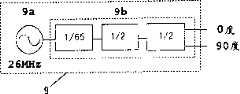
同样,第二正交混频器部分8被设置成其操作状态,改变开关部分10被设置接通第二正交混频器部分8端。此时,第二本机振荡器部分9的输出频率为100kHz,该频率值几乎等于失谐1/2信道间隔的频率。如果26MHz频率被用作GSM的基准信号,就能够获得260频分,如图6所示。在这种情况下,第二信道选择滤波器部分11确保衰减值,该衰减值在第一信道选择滤波器部分6中不足。Also, the second quadrature mixer section 8 is set to its operating state, and the
相反,将参照图3说明将接收机转换成ZIF接收机模式的情况,即CDMA系统的接收。第一本机振荡器部分5的输出频率被设置成几乎与接收频率相等的频率,第二正交混频器部分8和第二本机振荡器部分9的操作被停止,改变开关部分10被设置成接通可变增益放大器部分7的输出信号。第一信道选择滤波器部分6和第二信道选择滤波器部分11的总滤波器特性变成宽带LPF,该LPF使3.84Mcps的基带信号通过,这正是W-CDMA的传输速度并且对相邻信道信号带宽进行滤波。在“2000 IEEE Radio Frequency IntegratedCircuit Symposium MOM3B-2 Analog Baseband IC for use in direct conversionWCDMA receiver”中宣布了具体示例,其中,带宽将近2MHz。认为截止频率大约为20kHz的HPF是适合的,该值对接收特性没有影响。On the contrary, the case of switching the receiver to the ZIF receiver mode, that is, the reception of the CDMA system will be described with reference to FIG. 3 . The output frequency of the first
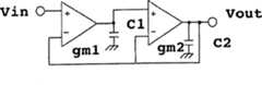
然后,示出各部分中的特性转换以便使LIF接收机和ZIF接收机协调操作的特定示例。如果利用gm-C滤波器来构造第一信道选择滤波器部分6和第二信道选择滤波器部分11,就能够简单地改变频率。通常,通过利用组合LPF和HPF来构造信道选择滤波器n(1,2,3...)。下面将以辅助LPF和主HPF为例来进行说明。Then, a specific example of characteristic conversion in each part in order to make the LIF receiver and the ZIF receiver operate in harmony is shown. If the first channel selection filter section 6 and the second channel
首先,图7示出辅助双二次(biquad)LPF作为LPF的结构示例,以下给出传递函数H(s)和角频率ω及Q。在本例中,图7所示的辅助双二次LPF(gm-C滤波器)由gm1,gm2,C1和C2组成。First, FIG. 7 shows an auxiliary biquad LPF as an example of the structure of the LPF, and the transfer function H(s) and angular frequencies ω and Q are given below. In this example, the auxiliary biquad LPF (gm-C filter) shown in Fig. 7 consists of gm1 , gm2 , C1 and C2 .
接着,图8示出构成滤波器的gm放大器,以下给出gm值。在本例中,通过电流源25、26和差分对管27来构造gm放大器。下列表达式中,Vt是热电压,Io是gm放大器的操作电流。Next, FIG. 8 shows a gm amplifier constituting a filter, and gm values are given below. In this example, a gm amplifier is constructed by
根据以上公式中的关系,可以理解LPF的截止频率和Q值能够由图7所示的gm放大器1的gm1和gm放大器2的gm2来控制。同样,由于gm能够由gm放大器的操作电流Io来控制,可以通过控制各gm放大器的操作电流以便改变滤波器的截止频率和Q值,来将接收机设置成LIF接收机模式和ZIF接收机模式中的每种接收机模式。According to the relationship in the above formula, it can be understood that the cut-off frequency and Q value of the LPF can be controlled by
同样,通过使用图9所示的DA变换器来改变gm放大器的操作电流值,能够实现频率特性的设置。由差分对晶体管28、可变电流电流源29、30、33、电流控制开关31和控制信号的串-并变换器部分32来构造图9所示的DA变换器。同样,可以在存储电路例如ROM,RAM等中,将各无线电系统和各接收机模式的设置规定成特征标准值,然后通过根据情况读取这些值来执行设置以便控制DA变换器。此时,可变电流电流源29、30、33充当DA变换器。Also, by changing the operating current value of the gm amplifier using the DA converter shown in FIG. 9, setting of the frequency characteristic can be realized. The DA converter shown in FIG. 9 is constructed by a differential pair of transistors 28, variable current current sources 29, 30, 33, a current control switch 31, and a serial-to-parallel converter section 32 of control signals. Also, setting of each radio system and each receiver mode can be specified as characteristic standard values in a storage circuit such as ROM, RAM, etc., and then setting is performed by reading these values according to the situation to control the DA converter. At this time, the variable current current sources 29, 30, 33 act as DA converters.
此外,在由于电路元件变化引起频率特性变化的情况下,如图10的流程图所示,通过在工厂进行调整时,检测GSM和W-CDMA的各接收状态的误差,这些误差偏离信道选择滤波器的频率特性的预定标准值,接着用标准值作为各个初始值来代替调整之后的校正值以便校正频率特性,就可以吸收滤波器的频率变化,这些初始值是控制gm放大器的设置信息。In addition, in the case of changes in frequency characteristics due to changes in circuit elements, as shown in the flow chart of Fig. 10, errors in each reception state of GSM and W-CDMA are detected by making adjustments at the factory, and these errors deviate from the channel selection filter The frequency variation of the filter can be absorbed by using predetermined standard values of the frequency characteristics of the filter, and then replacing the adjusted correction values with the standard values as respective initial values, which are setting information for controlling the gm amplifier, so as to correct the frequency characteristics.
接着,图11示出主HPF作为HPF的结构示例,给出传递函数H(s)和角频率ω。在本例中,图11所示的主HPF由gm3和C3组成。Next, FIG. 11 shows the main HPF as a configuration example of the HPF, giving the transfer function H(s) and the angular frequency ω. In this example, the main HPF shown in Figure 11 consists of gm3 and C3 .
与图7所示的辅助双二次LPF相似,由于可以利用电流控制gm放大器来改变截止频率,该主HPF也能够被设置成LIF接收机模式和ZIF接收机模式。同样,与LPF相似,在该HPF中,也可以在存储电路例如ROM、RAM等中,将各无线电系统和各接收机模式的设置规定成特征标准值,然后通过根据情况读取这些值来执行设置以便控制DA变换器。同样,采用与图10的流程图所示的方法相同的方式,通过用标准值作为各个初始值来代替调整之后的校正值以便校正频率特性,就可以吸收滤波器的频率变化,这些初始值是控制gm放大器的设置信息。在本例中,使用上述gm-C滤波器来进行说明,如果改变其频率特性,可以采用任何结构。Similar to the auxiliary biquad LPF shown in Fig. 7, the main HPF can also be set in LIF receiver mode and ZIF receiver mode since the cutoff frequency can be changed by using the current control gm amplifier. Also, similarly to LPF, in this HPF, the settings of each radio system and each receiver mode can be specified as characteristic standard values in storage circuits such as ROM, RAM, etc., and then executed by reading these values according to the situation Set to control the DA converter. Also, in the same manner as the method shown in the flowchart of FIG. 10, it is possible to absorb the frequency variation of the filter by replacing the corrected values after adjustment with standard values as respective initial values, which are Controls settings information for the gm amplifier. In this example, the above-mentioned gm-C filter is used for explanation, but any configuration can be adopted if its frequency characteristics are changed.
接下来,将参照图12和图13说明高频放大器部分3的结构示例。在GSM系统中,当前主要使用900MHz频带和1.8GHz频带。同样,在W-CDMA系统中,主要使用2GHz频带。因此,如图12所示,通过将高频放大器3a、3b、3c调整到各个频带,高频放大器部分3就能够处理各个频带。同样,在高频放大器部分3被构造成可变增益放大器的情况下,如果用于900MHz频带的高频放大器3a为例,可以通过添加高频放大器3d和衰减器3e,然后由偏置控制3h来转换高频放大器3f和增益控制开关3g,来实现这种放大器,如图13所示。在图13中,可变增益被说明为2级值。但是,可以采用多值类型和连续可变类型。同样,可以形成各频带,以具有相同的结构。Next, a structural example of the high-
接下来,将参照图14说明第一本机振荡器部分5。第一振荡器5a是频率合成器,移相器5b由第一分频器(1/2)5c和第二分频器(1/2)5d组成。在本例中,这些分频器是ECL型FF,并且输出同时1/2分频的正交相位信号。Next, the first
如果第一振荡器5a能够输出大约3.6GHz到4GHz的频率,那么利用第一分频器5c和第二分频器5d将第一振荡器5a输出的3.6GHz划分成1/4频率,就能够获得900MHz频带,还能够获得正交相位输出5e。利用第一分频器5c将第一振荡器5a输出的3.6GHz划分成1/2频率,就能够获得1.8GHz频带,还能够获得正交相位输出5f。类似地,利用第一分频器5c将第一振荡器5a输出的4GHz划分成1/2频率,就能够获得2 GHz频带,还能够获得正交相位输出5f。If the first oscillator 5a can output a frequency of about 3.6GHz to 4GHz, then the 3.6GHz output by the first oscillator 5a is divided into 1/4 frequency by using the
接下来,将参照图15和图16说明选择第一正交混频器部分4的频带的方法。图15能够实现频带选择。从高频放大器部分3输入的频率是900MHz频带、1.8GHz频带和2GHz频带,第一本机振荡器部分5具有900MHz频带、1.8GHz频带和2GHz频带,这些频带与各接收频率带宽相对应。高频放大器部分3和第一本机振荡器部分5的输出由高频开关4c、4d、4e选择以便设置所需频率。Next, a method of selecting the frequency band of the first
以下将参照图16说明高频开关4c。图16是示出高频开关4c示例的电路结构图。通过利用选择器开关4i对第一发射极跟随器4f、第二发射极跟随器4g和第三发射极跟随器4h的各基极偏压进行开/关控制,能够切换输入信号。只要能够进行输入信号的选择/切换,可以采用任何类型的开关,例如差分放大器、二极管等。在本例中,如果图16所示的高频开关4c被用作两组二进制开关,能够选择第一本机振荡器部分5的信号。The high-
以下将参照图17和图18说明可变增益放大器部分7。可变增益放大器部分7由电流源7c、7d、差分对7e、可变差分对发射极电阻7f和负载电阻7g、7h构成。可变增益放大器部分7的增益由差分对7e和可变差分对发射极电阻7f决定。同样,可以获得可变增益放大器部分7的输出为gm和负载电阻的乘积,其中gm由差分对7e和可变差分对发射极电阻7f决定。可向可变差分对发射极电阻7f提供多个抽头,并且可以利用由MOSFET等形成的开关调整电阻值来改变增益。The variable
如果可变增益放大器被多级级联,如图18所示的可变增益放大器7I、7j,就能够实现较宽的增益变化。同样,通过串-并变换器电路,能够将可变增益放大器的增益变换成几个比特的串行数据控制7k、7l。同样,如果接收系统所需的增益根据无线电系统或接收机模式(LIF接收机模式和ZIF接收机模式)而不同,通过使用可变增益放大器来设置增益的标准值。同样,设置信息作为各无线电系统或各接收机模式的特征标准值,可以被设置在例如ROM,RAM等的存储电路中,通过根据情况读取这种信息来执行设置。此外,对于由于电路元件变化所引起的增益变化,如图19的流程图所示,通过在工厂进行调整时检测增益标准值的误差,接着用标准值代替调整之后的用于可变增益放大器控制的设置信息以便校正增益,就可以吸收这种增益变化。If variable gain amplifiers are cascaded in multiple stages, such as
如上所述,根据本实施例的接收机,能够在无需提供特定偏移电压消除电路的情况下,提供适合于多种通信系统(TDMA系统和CDMA系统)的多模式接收机。As described above, according to the receiver of the present embodiment, it is possible to provide a multi-mode receiver suitable for various communication systems (TDMA system and CDMA system) without providing a specific offset voltage canceling circuit.
(第二实施例)(second embodiment)
以下将参照图20到图22说明根据本发明第二实施例的接收机。在第一实施例中,说明了由于能够利用HPF消除偏移电压,所以无需特定偏移电压消除电路,其中,偏移电压是由于在例如第一正交混频器部分4、第一信道选择滤波器部分6和可变增益放大器部分7等信号系统中结合采用LIF接收机模式或ZIF接收机模式而产生的。但是,在LIF接收机模式中,正如上面已经说明的,不能将消除偏移电压的HPF放置在模拟I、Q的基带输出中,该基带输出充当数字基带部分的接口。因此,如果解码部分12中不允许偏移电压,就可以提供偏移电压消除电路。A receiver according to a second embodiment of the present invention will be described below with reference to FIGS. 20 to 22. FIG. In the first embodiment, it was explained that a specific offset voltage canceling circuit is not required since the offset voltage due to an offset voltage in, for example, the first
图20示出第二信道选择滤波器部分11和解码部分12之间的接口部分,其中,第二信道选择滤波器部分11给出I、Q基带信号的输出。以下将参照图21和图22的流程图来说明偏移电压消除电路的示例。将I、Q分量的模拟基带输出电位11c、11d与参考电位11e进行比较,然后通过使用AD变换器(ADC)12a、12b、偏移电压调整部分12h、DA变换器(DAC)12l、12m和加法器11h,11i进行调整,以便最小化它们之间的差值。通常,这种调整在工厂进行,并且将DAC控制值设置在例如ROM、RAM等的存储电路12k中作为设置信息,然后在接收操作时通过读取这些值来执行设置。所以,仅使用简单的偏移电压消除,即仅通过在工厂发送时执行调整,就能够获得更稳定的接收特性。FIG. 20 shows an interface section between the second channel
(第三实施例)(third embodiment)
以下将说明根据本发明第三实施例的接收机。正如在第一实施例中所说明的,能够改变第一信道选择滤波器部分6和第二信道选择滤波器部分11的各频率特性和Q值。因此,能够设置频率特性和Q值使其满足任何通信系统。所以,适合于任何通信系统的接收机能够被构造在可接收的频带中。A receiver according to a third embodiment of the present invention will be described below. As explained in the first embodiment, each frequency characteristic and Q value of the first channel selection filter section 6 and the second channel
在第一和第二实施例中,说明了应用于W-CDMA和GSM的多模式接收机。但是,本发明不限于这些无线电系统,而是可以应用于模拟通信系统例如AMP等。同样,如果即使在TDMA系统中通信系统也能够满足ZIF接收机模式的无线电标准,本发明的接收机也可以用于ZIF接收机模式。此外,如果即使在CDMA系统中通信系统也能够满足LIF接收机模式的无线电标准,本发明的接收机也可以用于LIF接收机模式。In the first and second embodiments, multi-mode receivers applied to W-CDMA and GSM are described. However, the present invention is not limited to these radio systems, but can be applied to analog communication systems such as AMP and the like. Also, if the communication system can satisfy the radio standard of the ZIF receiver mode even in the TDMA system, the receiver of the present invention can also be used in the ZIF receiver mode. Furthermore, if the communication system can satisfy the radio standard of the LIF receiver mode even in the CDMA system, the receiver of the present invention can also be used in the LIF receiver mode.
同样,如果图1所示的解码部分12的CDMA解码部分12e和TDMA解码部分12f被构造成模块,或者如果利用软件改变能够被解码的无线电通信系统,或者如果采用两种结构,就可以允许从W-CDMA到IS95的改变或从GSM到PHS的改变。结果,能够实现适合于多种通信系统的接收机。此外,当接收机打算利用例如PDC和GSM等处理国际漫游时,并不需要一个各无线电通信系统之外的系统。因此,能够仅通过改变解码部分,来简单地改变相应的通信系统。Likewise, if the
(第四实施例)(fourth embodiment)
以下将说明根据本发明第四实施例的接收机。在第一、第二和第三实施例中,说明了多模式接收机。在使用TDMA系统或CDMA系统的单模式接收机中,尽管至此对于每个无线电通信系统,接收机都是利用专用集成电路来构造的,如果这种接收机在使用中被固定于LIF接收机模式或ZIF接收机模式,能够利用相同的集成电路来构造适合于各种无线电通信系统的接收机。A receiver according to a fourth embodiment of the present invention will be described below. In the first, second and third embodiments, multi-mode receivers are described. In a single-mode receiver using a TDMA system or a CDMA system, although for every radio communication system hitherto, the receiver is constructed using an ASIC, if such a receiver is fixed in use in the LIF receiver mode Or ZIF receiver mode, the same integrated circuit can be used to construct receivers suitable for various radio communication systems.
在这种情况下,在第一和第二实施例中已经说明了这种接收机。但是可以通过组合相关接收机和发射机来构造通信终端。In this case, the receiver has been explained in the first and second embodiments. But it is possible to construct a communication terminal by combining related receivers and transmitters.
而且,本发明基于于2001年7月27日提交的日本专利申请No.2001-228063,其内容以引用方式包含在本文的内容中。Also, the present invention is based on Japanese Patent Application No. 2001-228063 filed on July 27, 2001, the contents of which are incorporated herein by reference.
产业上的可利用性Industrial availability
如上所述,根据本发明的接收机和通信终端,能够在无需提供特定偏移电压消除电路的情况下,提供适合于多种通信系统(TDMA系统和CDMA系统)的多模式接收机和通信终端。同样,能够利用相同的结构提供适合于任何一种通信系统的接收机和通信终端。As described above, according to the receiver and communication terminal of the present invention, it is possible to provide a multi-mode receiver and communication terminal suitable for various communication systems (TDMA system and CDMA system) without providing a specific offset voltage canceling circuit . Also, a receiver and a communication terminal suitable for any communication system can be provided with the same structure.
Claims (5)
Translated fromChineseApplications Claiming Priority (2)
| Application Number | Priority Date | Filing Date | Title |
|---|---|---|---|
| JP228063/2001 | 2001-07-27 | ||
| JP2001228063AJP3700933B2 (en) | 2001-07-27 | 2001-07-27 | Receiver and communication terminal |
Publications (1)
| Publication Number | Publication Date |
|---|---|
| CN1529947Atrue CN1529947A (en) | 2004-09-15 |
Family
ID=19060625
Family Applications (1)
| Application Number | Title | Priority Date | Filing Date |
|---|---|---|---|
| CNA028143248APendingCN1529947A (en) | 2001-07-27 | 2002-06-04 | receivers and communication terminals |
Country Status (5)
| Country | Link |
|---|---|
| US (1) | US20040218576A1 (en) |
| EP (1) | EP1414163A1 (en) |
| JP (1) | JP3700933B2 (en) |
| CN (1) | CN1529947A (en) |
| WO (1) | WO2003013013A1 (en) |
Cited By (6)
| Publication number | Priority date | Publication date | Assignee | Title |
|---|---|---|---|---|
| CN101860505A (en)* | 2009-04-07 | 2010-10-13 | 斯沃奇集团研究和开发有限公司 | The high sensitivity fsk modulated signal receiver of low rate mode |
| CN101044683B (en)* | 2004-10-18 | 2011-01-12 | Nxp股份有限公司 | Device for processing analog input signal and mobile communication device comprising same |
| CN101965699A (en)* | 2008-03-13 | 2011-02-02 | 索尼爱立信移动通讯有限公司 | Automatic optimization of rf receiver interference performance |
| US8208883B2 (en) | 2008-02-14 | 2012-06-26 | Silicon Motion, Inc. | Receiver with low power consumption |
| CN103546179A (en)* | 2012-07-16 | 2014-01-29 | 英特尔移动通信有限责任公司 | Receiver, method and mobile communication device |
| CN104247275A (en)* | 2012-04-25 | 2014-12-24 | 高通股份有限公司 | Combining multiple desired signals into a single baseband signal |
Families Citing this family (27)
| Publication number | Priority date | Publication date | Assignee | Title |
|---|---|---|---|---|
| JP3770819B2 (en)* | 2001-09-28 | 2006-04-26 | 株式会社ルネサステクノロジ | Wireless communication receiver |
| DE10228757A1 (en)* | 2002-06-27 | 2004-01-22 | Infineon Technologies Ag | Receiver arrangement, especially for mobile radio |
| EP1704649B1 (en)* | 2003-02-07 | 2009-12-30 | Nxp B.V. | Versatile baseband signal input current splitter |
| JP2005101693A (en)* | 2003-09-22 | 2005-04-14 | Hitachi Kokusai Electric Inc | Receiving machine |
| DE102004022324A1 (en)* | 2004-05-06 | 2005-12-01 | Infineon Technologies Ag | Signal conditioning circuit, in particular for a receiver arrangement for mobile communications |
| US20060068746A1 (en)* | 2004-09-30 | 2006-03-30 | Nokia Corporation | Direct conversion receiver radio frequency integrated circuit |
| JP4584668B2 (en)* | 2004-10-07 | 2010-11-24 | Okiセミコンダクタ株式会社 | Automatic gain control circuit and method |
| WO2006043533A1 (en)* | 2004-10-19 | 2006-04-27 | Matsushita Electric Industrial Co., Ltd. | Receiver |
| US20060093069A1 (en)* | 2004-10-29 | 2006-05-04 | Pan Meng-An Michael | Method and system for sharing GM stage for a second if mixer using a polyphase clock to reduce current consumption and improve matching |
| CN101120509B (en)* | 2005-02-14 | 2012-06-13 | 皇家飞利浦电子股份有限公司 | Receiver for simultaneously receiving different standards |
| JP2007074187A (en)* | 2005-09-06 | 2007-03-22 | Matsushita Electric Ind Co Ltd | Multi-mode signal processor |
| DE602006007071D1 (en)* | 2005-09-16 | 2009-07-16 | Toshiba Kk | Analog signal processing circuit and communication device with it |
| US7684523B2 (en)* | 2005-09-28 | 2010-03-23 | Lg Electronics Inc. | Method and apparatus for channel estimation |
| US7769359B2 (en)* | 2006-06-08 | 2010-08-03 | O2Micro International Ltd. | Adaptive wireless receiver |
| US7978773B2 (en)* | 2006-12-29 | 2011-07-12 | Agere Systems Inc. | Multi-channel receiver with improved AGC |
| US8812052B2 (en) | 2007-02-27 | 2014-08-19 | Qualcomm Incorporated | SPS receiver with adjustable linearity |
| US7809343B2 (en) | 2007-04-25 | 2010-10-05 | Agere Systems Inc. | Multi-channel receiver with improved AGC |
| US7769357B2 (en)* | 2007-04-25 | 2010-08-03 | Agere Systems Inc. | Multi-channel receiver with improved AGC |
| JP4755666B2 (en)* | 2008-03-28 | 2011-08-24 | 日本電信電話株式会社 | Wireless communication module |
| JP5005622B2 (en)* | 2008-06-30 | 2012-08-22 | シャープ株式会社 | Receiving device, tuner, and television receiver |
| JP2010028652A (en)* | 2008-07-23 | 2010-02-04 | Omron Corp | Signal processing device, signal processing method, reception device, transmission/reception device, communication module, and electronic device |
| JP5627186B2 (en)* | 2009-03-05 | 2014-11-19 | 三菱電機株式会社 | Anomaly monitoring device for electrical equipment and anomaly monitoring device for accelerator device |
| US9231630B2 (en)* | 2009-05-05 | 2016-01-05 | San Diego, CA | Radio device having dynamic intermediate frequency scaling |
| US8264392B1 (en)* | 2009-12-09 | 2012-09-11 | Marvell International Ltd. | Compact high-speed analog-to-digital converter for both I and Q analog to digital conversion |
| JP5846840B2 (en) | 2011-10-14 | 2016-01-20 | ルネサスエレクトロニクス株式会社 | Filter circuit and receiver |
| FR3012275B1 (en)* | 2013-10-18 | 2015-12-25 | Commissariat Energie Atomique | UWB RECEIVER WITH INTERMITTENT OPERATION |
| KR101692242B1 (en)* | 2014-12-16 | 2017-01-04 | (주)에프씨아이 | Apparatus for Transmitting and Receiving Signal in Radio Frequency System |
Family Cites Families (17)
| Publication number | Priority date | Publication date | Assignee | Title |
|---|---|---|---|---|
| US5319634A (en)* | 1991-10-07 | 1994-06-07 | Phoenix Corporation | Multiple access telephone extension systems and methods |
| US5260967A (en)* | 1992-01-13 | 1993-11-09 | Interdigital Technology Corporation | CDMA/TDMA spread-spectrum communications system and method |
| US5614914A (en)* | 1994-09-06 | 1997-03-25 | Interdigital Technology Corporation | Wireless telephone distribution system with time and space diversity transmission for determining receiver location |
| JP3215018B2 (en)* | 1994-09-09 | 2001-10-02 | 三菱電機株式会社 | Mobile communication system |
| US5790549A (en)* | 1996-02-29 | 1998-08-04 | Ericsson Inc. | Subtractive multicarrier CDMA access methods and systems |
| JP3506562B2 (en)* | 1996-06-27 | 2004-03-15 | 松下電器産業株式会社 | Direct conversion receiver |
| US5974305A (en)* | 1997-05-15 | 1999-10-26 | Nokia Mobile Phones Limited | Dual band architectures for mobile stations |
| US6975673B1 (en)* | 1998-07-14 | 2005-12-13 | Axonn, L.L.C. | Narrow-band interference rejecting spread spectrum radio system and method |
| JP3911861B2 (en)* | 1998-07-22 | 2007-05-09 | ソニー株式会社 | COMMUNICATION METHOD, TRANSMISSION POWER CONTROL METHOD, AND MOBILE STATION |
| US7593481B2 (en)* | 1998-08-31 | 2009-09-22 | Kamilo Feher | CDMA, W-CDMA, 3rd generation interoperable modem format selectable (MFS) systems with GMSK modulated systems |
| GB2341993B (en)* | 1998-09-25 | 2003-03-12 | Nec Technologies | Radio receivers |
| US6741551B1 (en)* | 1999-01-11 | 2004-05-25 | International Business Machines Corporation | Hybrid TDMA/CDMA system based on filtered multitone modulation |
| EP1083669B1 (en)* | 1999-03-11 | 2004-10-27 | Mitsubishi Denki Kabushiki Kaisha | Radio terminal device |
| US6608858B1 (en)* | 2000-01-26 | 2003-08-19 | Qualcomm Incorporated | Multipath doppler adjusted frequency tracking loop |
| US20030067964A1 (en)* | 2000-02-10 | 2003-04-10 | Daoben Li | Code-division-multiple-access system using zero correlation window |
| US6711144B1 (en)* | 2000-09-15 | 2004-03-23 | Airvana, Inc. | Multi-user communication of voice and data |
| CN1146171C (en)* | 2000-11-24 | 2004-04-14 | 华为技术有限公司 | Realization Method of Large Capacity Synchronous Code Division Multiple Access Spread Spectrum Communication System |
- 2001
- 2001-07-27JPJP2001228063Apatent/JP3700933B2/ennot_activeExpired - Fee Related
- 2002
- 2002-06-04EPEP20020730904patent/EP1414163A1/ennot_activeWithdrawn
- 2002-06-04USUS10/484,558patent/US20040218576A1/ennot_activeAbandoned
- 2002-06-04WOPCT/JP2002/005491patent/WO2003013013A1/ennot_activeCeased
- 2002-06-04CNCNA028143248Apatent/CN1529947A/enactivePending
Cited By (12)
| Publication number | Priority date | Publication date | Assignee | Title |
|---|---|---|---|---|
| CN101044683B (en)* | 2004-10-18 | 2011-01-12 | Nxp股份有限公司 | Device for processing analog input signal and mobile communication device comprising same |
| US8208883B2 (en) | 2008-02-14 | 2012-06-26 | Silicon Motion, Inc. | Receiver with low power consumption |
| CN101510786B (en)* | 2008-02-14 | 2013-01-23 | 慧国(上海)软件科技有限公司 | Receiver with low power consumption |
| CN101965699A (en)* | 2008-03-13 | 2011-02-02 | 索尼爱立信移动通讯有限公司 | Automatic optimization of rf receiver interference performance |
| CN101965699B (en)* | 2008-03-13 | 2013-06-26 | 索尼爱立信移动通讯有限公司 | Automatic Optimization of RF Receiver Interference Performance |
| CN101860505A (en)* | 2009-04-07 | 2010-10-13 | 斯沃奇集团研究和开发有限公司 | The high sensitivity fsk modulated signal receiver of low rate mode |
| CN101860505B (en)* | 2009-04-07 | 2014-04-30 | 斯沃奇集团研究和开发有限公司 | High-sensitivity, low-rate FSK modulation signal receiver |
| CN104247275A (en)* | 2012-04-25 | 2014-12-24 | 高通股份有限公司 | Combining multiple desired signals into a single baseband signal |
| US9673842B2 (en) | 2012-04-25 | 2017-06-06 | Qualcomm Incorporated | Combining multiple desired signals into a single baseband signal |
| CN104247275B (en)* | 2012-04-25 | 2017-11-24 | 高通股份有限公司 | Multiple desired signals are combined into the transceiver and method of single baseband signal |
| CN103546179A (en)* | 2012-07-16 | 2014-01-29 | 英特尔移动通信有限责任公司 | Receiver, method and mobile communication device |
| CN103546179B (en)* | 2012-07-16 | 2017-04-26 | 英特尔德国有限责任公司 | receiver, method and mobile communication device |
Also Published As
| Publication number | Publication date |
|---|---|
| JP3700933B2 (en) | 2005-09-28 |
| EP1414163A1 (en) | 2004-04-28 |
| US20040218576A1 (en) | 2004-11-04 |
| JP2003046401A (en) | 2003-02-14 |
| WO2003013013A1 (en) | 2003-02-13 |
Similar Documents
| Publication | Publication Date | Title |
|---|---|---|
| CN1529947A (en) | receivers and communication terminals | |
| KR100356004B1 (en) | Low noise gilbert multiplier cells and quadrature modulators, and related methods | |
| CN1192499C (en) | Method and arrangement for transmitting and receiving RF signals through various radio interfaces of communication systems | |
| US7899426B2 (en) | Degenerated passive mixer in saw-less receiver | |
| CN101061640A (en) | Direct conversation receiver radio frequency integrated circuit | |
| CN1134902C (en) | Circuit arrangement for multistandard communication terminal | |
| CN1169296C (en) | PLL circuit and wireless communication terminal using the circuit | |
| US8145170B2 (en) | Low-cost receiver using tracking bandpass filter and lowpass filter | |
| CN1639992A (en) | Distortion reduction calibration | |
| JP6462541B2 (en) | Complex bandpass filter and receiver | |
| CN1243371A (en) | Direct-convertion receiver | |
| US7515648B2 (en) | Transmitter and wireless communication apparatus using same | |
| CN1496014A (en) | Receiving device and gain control method | |
| JP3816356B2 (en) | Wireless transmitter | |
| CN1146122C (en) | wireless terminal device | |
| CN1204696C (en) | Wide band tuner | |
| CN1108066C (en) | Selective paging wireless receiver using direct conversion method | |
| US7202916B2 (en) | Television tuner and method of processing a received RF signal | |
| CN1481617A (en) | Direct Conversion Digital Domain Control | |
| JP2006101478A (en) | Semiconductor integrated circuit for communication, and wireless communications system | |
| US7511557B2 (en) | Quadrature mixer circuit and RF communication semiconductor integrated circuit | |
| JP2007228342A (en) | Receiver and transmitter-receiver using same | |
| CN1801604A (en) | Signal processing circuit and communication device using the same | |
| CN1197261C (en) | Frequency conversion circuit and communication device | |
| CN1639990A (en) | 3G radio device |
Legal Events
| Date | Code | Title | Description |
|---|---|---|---|
| C06 | Publication | ||
| PB01 | Publication | ||
| C10 | Entry into substantive examination | ||
| SE01 | Entry into force of request for substantive examination | ||
| C02 | Deemed withdrawal of patent application after publication (patent law 2001) | ||
| WD01 | Invention patent application deemed withdrawn after publication |