CN1527948A - Low jitter clock for test system - Google Patents
Low jitter clock for test systemDownload PDFInfo
- Publication number
- CN1527948A CN1527948ACNA028069587ACN02806958ACN1527948ACN 1527948 ACN1527948 ACN 1527948ACN A028069587 ACNA028069587 ACN A028069587ACN 02806958 ACN02806958 ACN 02806958ACN 1527948 ACN1527948 ACN 1527948A
- Authority
- CN
- China
- Prior art keywords
- test
- frequency
- signal
- clock signals
- mode signal
- Prior art date
- Legal status (The legal status is an assumption and is not a legal conclusion. Google has not performed a legal analysis and makes no representation as to the accuracy of the status listed.)
- Pending
Links
Images


Classifications
- G—PHYSICS
- G01—MEASURING; TESTING
- G01R—MEASURING ELECTRIC VARIABLES; MEASURING MAGNETIC VARIABLES
- G01R31/00—Arrangements for testing electric properties; Arrangements for locating electric faults; Arrangements for electrical testing characterised by what is being tested not provided for elsewhere
- G01R31/28—Testing of electronic circuits, e.g. by signal tracer
- G01R31/317—Testing of digital circuits
- G01R31/31708—Analysis of signal quality
- G01R31/31709—Jitter measurements; Jitter generators
- G—PHYSICS
- G01—MEASURING; TESTING
- G01R—MEASURING ELECTRIC VARIABLES; MEASURING MAGNETIC VARIABLES
- G01R31/00—Arrangements for testing electric properties; Arrangements for locating electric faults; Arrangements for electrical testing characterised by what is being tested not provided for elsewhere
- G01R31/28—Testing of electronic circuits, e.g. by signal tracer
- G01R31/317—Testing of digital circuits
- G01R31/3181—Functional testing
- G01R31/3185—Reconfiguring for testing, e.g. LSSD, partitioning
- G01R31/318505—Test of Modular systems, e.g. Wafers, MCM's
- G—PHYSICS
- G01—MEASURING; TESTING
- G01R—MEASURING ELECTRIC VARIABLES; MEASURING MAGNETIC VARIABLES
- G01R31/00—Arrangements for testing electric properties; Arrangements for locating electric faults; Arrangements for electrical testing characterised by what is being tested not provided for elsewhere
- G01R31/28—Testing of electronic circuits, e.g. by signal tracer
- G01R31/317—Testing of digital circuits
- G01R31/3181—Functional testing
- G01R31/319—Tester hardware, i.e. output processing circuits
- G01R31/31917—Stimuli generation or application of test patterns to the device under test [DUT]
- G01R31/31922—Timing generation or clock distribution
- G—PHYSICS
- G01—MEASURING; TESTING
- G01R—MEASURING ELECTRIC VARIABLES; MEASURING MAGNETIC VARIABLES
- G01R31/00—Arrangements for testing electric properties; Arrangements for locating electric faults; Arrangements for electrical testing characterised by what is being tested not provided for elsewhere
- G01R31/28—Testing of electronic circuits, e.g. by signal tracer
- G01R31/317—Testing of digital circuits
- G01R31/3181—Functional testing
- G01R31/319—Tester hardware, i.e. output processing circuits
- G01R31/3193—Tester hardware, i.e. output processing circuits with comparison between actual response and known fault free response
- G01R31/31937—Timing aspects, e.g. measuring propagation delay
- G—PHYSICS
- G11—INFORMATION STORAGE
- G11C—STATIC STORES
- G11C29/00—Checking stores for correct operation ; Subsequent repair; Testing stores during standby or offline operation
- G11C29/04—Detection or location of defective memory elements, e.g. cell constructio details, timing of test signals
- G11C29/08—Functional testing, e.g. testing during refresh, power-on self testing [POST] or distributed testing
- G11C29/10—Test algorithms, e.g. memory scan [MScan] algorithms; Test patterns, e.g. checkerboard patterns
- G—PHYSICS
- G11—INFORMATION STORAGE
- G11C—STATIC STORES
- G11C29/00—Checking stores for correct operation ; Subsequent repair; Testing stores during standby or offline operation
- G11C29/56—External testing equipment for static stores, e.g. automatic test equipment [ATE]; Interfaces therefor
- G—PHYSICS
- G11—INFORMATION STORAGE
- G11C—STATIC STORES
- G11C29/00—Checking stores for correct operation ; Subsequent repair; Testing stores during standby or offline operation
- G11C29/04—Detection or location of defective memory elements, e.g. cell constructio details, timing of test signals
- G11C2029/0401—Detection or location of defective memory elements, e.g. cell constructio details, timing of test signals in embedded memories
Landscapes
- Physics & Mathematics (AREA)
- Engineering & Computer Science (AREA)
- General Engineering & Computer Science (AREA)
- General Physics & Mathematics (AREA)
- Nonlinear Science (AREA)
- Tests Of Electronic Circuits (AREA)
- Stabilization Of Oscillater, Synchronisation, Frequency Synthesizers (AREA)
- For Increasing The Reliability Of Semiconductor Memories (AREA)
Abstract
Description
Translated fromChinese技术领域technical field
本申请涉及测试系统的时钟,用于产生测试模式和时钟信号,供测试电路,如测试集成电路装置之用。The present application relates to clocks for test systems for generating test patterns and clock signals for testing circuits, such as testing integrated circuit devices.
背景技术Background technique
测试高速集成电路装置(即待测试装置(DUT)),如微处理器,所使用的测试系统,由于必须产生精确的时钟信号和测试模式信号,变得越来越复杂。时钟信号是提供给DUT时钟输入引脚的,并用于运行该DUT,而测试模式则用于驱动并选通该DUT的数据引脚。Test systems for testing high speed integrated circuit devices (ie, devices under test (DUTs)), such as microprocessors, are becoming increasingly complex due to the need to generate precise clock signals and test mode signals. The clock signal is provided to the DUT clock input pin and used to run the DUT, while the test mode is used to drive and gate the DUT's data pins.
测试模式信号(亦称“事件序列”)一般包括事件模式,诸如二进制值(各个1和各个0),以及与每一事件的上升和下降缘的出现相关联的时间,一般称为测试周期。事件通常是两种事件类型中的一种—驱动某一DUT数据引脚到某一特定状态的驱动事件,和测试某一DUT数据引脚的状态的选通事件(亦称测试事件)。图1画出测试模式100的一个例子,该例子在测试某一DUT时可能发生。在该例子中,测试模式100包括四种事件。一种事件是一对(S,T),这里“S”是状态,“T”是与过渡到该状态相关联的时间。例如,测试模式100有四种驱动事件,可以写成(D1,1)、(D0,8)、(D1,13)、和(D0,18)。第一事件是在时间等于1时把信号驱动至高状态(1)。第二事件是在时间8时把信号驱动至低状态(0)。第三事件是在时间13时把信号驱动至高状态(1)。第四事件是在时间18时把信号驱动至低状态(0)。测试模式100的测试周期是在时间1到时间13之间的时间,对相继发生的驱动事件,重复该周期。A test pattern signal (also called an "event sequence") generally includes a pattern of events, such as binary values (each 1 and each 0), and a time associated with the occurrence of each event's rising and falling edges, generally referred to as a test period. Events are typically one of two event types—drive events, which drive a DUT data pin to a specific state, and strobe events (aka test events), which test the state of a DUT data pin. FIG. 1 depicts an example of a
在开发一种测试模式信号中,测试系统必须有一种机构来产生事件的模式,可以参考测试系统的主时钟,把事件模式中的上升和下降缘,按精确的时间置于选择的测试周期内。假定主时钟的周期是2.5纳秒(ns),那么测试系统应能以10皮秒(ps)量级的精度,设置上升/下降缘。如在图2中所示,要产生主时钟200周期倍数(如2.5ns或5.0ns)的测试周期的测试模式信号,可以通过用程序可控的分频器204完成。要产生主时钟200周期倍数中间(如2.7ns或5.5ns)的测试周期的测试模式信号,可以通过用微调电路210实现的微调技术完成,该微调技术向主时钟200周期或主时钟200周期倍数,提供程序可控的周期偏移212(亦称“周期微调”)。一般说来,用周期微调212的值来调整主时钟周期,以获得适合用于特定测试模式信号所需的测试周期216。测试系统,如在U.S.Pat.Nos.6,128,754,5,672,275,和5,212,443中所述的那些系统,说明如何使用微调技术来产生周期微调,本文引用这些专利公开的内容,供参考。In developing a test pattern signal, the test system must have a mechanism to generate a pattern of events that places the rising and falling edges of the event pattern at precise times within the selected test period by reference to the test system's master clock . Assuming a master clock with a period of 2.5 nanoseconds (ns), the test system should be able to set rising/falling edges with an accuracy on the order of 10 picoseconds (ps). As shown in FIG. 2 , to generate a test mode signal of a test period that is a multiple of 200 periods of the main clock (eg, 2.5 ns or 5.0 ns), can be accomplished by using a program-
因为微调技术是频率综合的一种数字方法,它一般有某些优点,诸如增加的灵活性(即易于把事件置于测试周期内的能力)和在运行时间内同时改变周期的能力。但是,微调电路固有的模拟本性,使得它是非线性的。微调电路的非线性,对测试周期的边缘布局精度和测试周期的周期到周期的抖动,有巨大影响。典型的周期到周期抖动值,可达20ps。在频谱分析仪上,抖动典型地表现为在频率上分开的尖刺,而基于微调的时钟是按该频率运转的。Because the fine-tuning technique is a digital approach to frequency synthesis, it generally has certain advantages, such as increased flexibility (ie, the ability to easily place events within the test cycle) and the ability to simultaneously change the cycle at runtime. However, the inherent analog nature of the trimming circuit makes it non-linear. The nonlinearity of the trimming circuit has a huge impact on the edge placement accuracy of the test cycle and the cycle-to-cycle jitter of the test cycle. Typical cycle-to-cycle jitter values can reach 20ps. On a spectrum analyzer, jitter typically appears as spikes separated by the frequency at which the trimming-based clock operates.
用于运行DUT的时钟信号,一般必须与测试模式信号在相位上同步且频率相似。频率相似意味着时钟信号是测试模式信号的倍数或约数。一般说来,作为基于微调的时钟,是用于为DUT产生时钟信号的。The clock signal used to run the DUT typically must be synchronized in phase and similar in frequency to the test mode signal. Similar in frequency means that the clock signal is a multiple or submultiple of the test pattern signal. Generally speaking, as a clock based on trimming, it is used to generate a clock signal for the DUT.
发明内容Contents of the invention
本发明人认识到,使用基于周期微调的时钟为DUT产生测试模式信号和时钟信号的常规测试系统,能在运行时间内同时改变时钟周期、易于在测试周期内移动某一事件的出现、和提供带有一些周期到周期抖动的时钟信号。本发明人还认识到,与基于微调的时钟相关联的周期到周期的抖动,对某些应用,如结构测试,可能成为问题,因为在结构测试中,除了需要基于周期微调的时钟来改变周期的灵活性和在周期内移动事件的出现之外,DUT还需要低的周期到周期抖动的时钟输入。因此,本发明人利用周期微调来产生测试模式信号,开发出测试系统使用的低抖动的时钟。本发明人利用程序可控锁相环时钟,它能输出与产生的基于周期微调的测试模式信号频率相似且相位匹配的信号,从而开发出低抖动的时钟。The inventors have realized that a conventional test system that uses a clock based on period trimming to generate test mode signals and clock signals for the DUT can simultaneously vary the clock period during runtime, easily shift the occurrence of an event within the test period, and provide A clock signal with some cycle-to-cycle jitter. The inventors have also recognized that the cycle-to-cycle jitter associated with clocks based on trimming can be problematic for certain applications, such as structural testing, where, in addition to requiring a clock based on trimming to vary the period In addition to the flexibility and occurrence of intra-cycle shifting events, the DUT requires a clock input with low cycle-to-cycle jitter. Therefore, the present inventors have developed a low jitter clock for use in test systems by utilizing period trimming to generate test mode signals. The inventors have developed a low jitter clock by using a program-controllable phase-locked loop clock that can output a signal that is similar in frequency and phase-matched to the generated test mode signal based on period trimming.
这里说明的测试系统格式化程序的实现,可以包括如下特征的各种组合。Implementations of the test system formatter described herein may include various combinations of the following features.
一方面,测试系统使用的信号发生设备,包括:周期微调测试模式发生器,它可以编程,以便用微调技术来产生测试模式信号;和锁相环时钟,它可以编程,以便输出测试时钟信号,该测试时钟信号与该周期微调时钟产生的测试模式信号,频率相似(如为测试模式信号频率的倍数或约数)且相位匹配。每一周期微调测试模式发生器和锁相环时钟,是程序可控的,以便为不同类型的待测试装置,产生相应的测试模式信号和测试时钟信号。此外,该周期微调测试模式发生器是程序可控的,以便用比主周期约高两个或更多数量级的精度,把事件置于主周期内。On the one hand, the signal generating equipment used by the test system includes: a periodic fine-tuning test pattern generator, which can be programmed to generate test pattern signals with fine-tuning techniques; and a phase-locked loop clock, which can be programmed to output test clock signals, The test clock signal and the test mode signal generated by the period trimming clock have a similar frequency (for example, a multiple or submultiple of the frequency of the test mode signal) and a phase match. The fine-tuning of the test pattern generator and the phase-locked loop clock in each cycle is program-controllable, so as to generate corresponding test pattern signals and test clock signals for different types of devices to be tested. In addition, the cycle trim test pattern generator is programmable to place events within the main cycle with a precision of about two or more orders of magnitude greater than the main cycle.
该信号发生设备还可以包括主定时参考信号,该信号被送至每一个周期微调测试模式发生器及锁相环时钟。周期微调测试模式发生器可以包括全局定序器和一个或多个局部定序器。锁相环时钟可以包括乘法器、低通滤波器、压控振荡器、和反馈部分。锁相环时钟还可以包括程序可控延迟线和/或程序可控门,每一个都是可控的,以便在周期微调测试模式发生器的输出改变时,使锁相环时钟与周期微调测试模式发生器重新同步。The signal generating device may also include a master timing reference signal which is fed to each cycle to trim the test pattern generator and the phase locked loop clock. A cycle fine-tuning test pattern generator may include a global sequencer and one or more local sequencers. A phase locked loop clock may include a multiplier, a low pass filter, a voltage controlled oscillator, and a feedback section. The phase-locked loop clock may also include program-controllable delay lines and/or program-controllable gates, each of which is controllable to cause the phase-locked loop clock to cycle trim test when the output of the cycle trim test pattern generator changes. The pattern generator is resynchronized.
锁相环时钟可以包括一个或多个程序可控分频器,这些分频器是可控的,以便调整锁相环时钟的输出频率。这些分频器可以包括位于参考输入信号端的第一分频器、位于锁相环反馈部分的第二分频器、和位于锁相环输出端的第三分频器。在这种情况下,第一分频器可以是除以M的分频器,第二分频器可以是除以N的分频器,和第三分频器可以是除以D的分频器,其中M、N、和D是程序可控的整数系数。测试时钟信号的频率可由选择的M、N、和D控制,以便按下述方程式选择需要的输出频率FoutThe phase locked loop clock may include one or more program-controllable frequency dividers that are controllable to adjust the output frequency of the phase locked loop clock. These frequency dividers may include a first frequency divider at the reference input signal terminal, a second frequency divider at the PLL feedback section, and a third frequency divider at the PLL output. In this case, the first divider can be a divide-by-M divider, the second divider can be a divide-by-N divider, and the third divider can be a divide-by-D divider device, where M, N, and D are program-controllable integer coefficients. The frequency of the test clock signal can be controlled by the selected M, N, and D, so that the required output frequency Fout can be selected according to the following equation
这里Fref是参考输入信号。N可以与周期分辨率对应,且例如可以设为64。D可以与粗频率调整对应和N可以与细频率调整对应。在一个实施例中,D是2的乘方。Here Fref is the reference input signal. N may correspond to the period resolution, and may be set to 64, for example. D may correspond to coarse frequency adjustment and N may correspond to fine frequency adjustment. In one embodiment, D is a power of two.
另一方面,测试信号可以由用微调技术产生的测试模式信号产生,并用锁相环产生一个与测试模式信号频率相似且相位匹配的测试时钟信号。产生的测试模式信号和相位匹配的测试时钟信号,可以加到待测试的装置上。具体说,把产生的测试模式信号加到待测试装置的数据引脚上,和把相位匹配的测试时钟信号加到待测试装置的输入引脚上。相位匹配的测试时钟信号,可以通过用锁相环使测试时钟信号与测试模式信号同步而产生。产生一个相位匹配的测试时钟信号,还可以包括根据公共的主时钟参考,产生测试模式信号和测试时钟信号。On the other hand, the test signal can be generated from the test mode signal generated by trimming technique, and a phase-locked loop is used to generate a test clock signal with similar frequency and phase matching with the test mode signal. The generated test mode signal and phase matched test clock signal can be applied to the device under test. Specifically, the generated test mode signal is applied to the data pin of the device under test, and the phase matched test clock signal is applied to the input pin of the device under test. A phase-matched test clock signal can be generated by synchronizing the test clock signal with the test mode signal using a phase locked loop. Generating a phase-matched test clock signal may also include generating a test mode signal and a test clock signal based on a common master clock reference.
此外,产生一个频率相似的测试时钟信号,可以包括使测试时钟信号的频率与测试模式信号基本上匹配。使测试时钟信号频率基本上匹配,可以包括控制一个或多个程序可控分频器,以便调整测试时钟信号,使之成为测试模式信号频率的倍数或约数。更普遍地说,控制测试时钟信号的频率,可以通过控制多个程序可控分频器来实现。Additionally, generating a test clock signal of a similar frequency may include substantially matching the frequency of the test clock signal to the test mode signal. Substantially matching the test clock signal frequency may include controlling one or more programmable frequency dividers to adjust the test clock signal to be a multiple or submultiple of the test mode signal frequency. More generally, controlling the frequency of the test clock signal can be achieved by controlling a plurality of programmable frequency dividers.
当测试模式信号的频率变化时,可以通过对一个或多个程序可控分频器改编程序,调整测试时钟信号的频率,使之与改变了的测试模式信号频率匹配。在这种情况下,可以通过控制延迟线或门或两者,改变测试时钟信号的定时,使测试时钟信号与测试模式信号再同步。When the frequency of the test mode signal changes, the frequency of the test clock signal can be adjusted to match the changed frequency of the test mode signal by reprogramming one or more programmable frequency dividers. In this case, the test clock signal can be resynchronized with the test mode signal by changing the timing of the test clock signal by controlling the delay line OR gate or both.
另一方面,为待测试装置产生测试信号,可以包括:产生主参考信号;根据该主参考信号,用微调技术产生测试模式信号;产生测试时钟信号,通过把主参考信号作为输入提供给锁相环,并控制锁相环内的一个或多个程序可控分频器,以调整该测试时钟信号,使之成为测试模式信号频率的倍数或约数,从而使该测试时钟信号与该测试模式信号相位匹配且频率相似;把该测试时钟信号加到待测试装置的时钟输入引脚;最后,把该测试模式信号加到待测试装置的数据引脚。当测试模式信号频率变化时,可以通过对一个或多个程序可控分频器改编程序,调整测试时钟信号频率,以校准测试模式信号变化了的频率。此外,可以通过控制延迟线或门或两者,改变测试时钟信号的定时,使测试时钟信号与测试模式信号再同步。On the other hand, generating a test signal for the device to be tested may include: generating a main reference signal; according to the main reference signal, using a fine-tuning technique to generate a test mode signal; generating a test clock signal, by providing the main reference signal as an input to the phase lock loop, and control one or more program-controllable frequency dividers in the phase-locked loop to adjust the test clock signal to make it a multiple or submultiple of the test mode signal frequency, so that the test clock signal and the test mode The signals are phase matched and of similar frequency; the test clock signal is applied to the clock input pin of the device under test; finally, the test mode signal is applied to the data pin of the device under test. When the frequency of the test mode signal changes, the frequency of the test clock signal can be adjusted by reprogramming one or more program-controllable frequency dividers to calibrate the changed frequency of the test mode signal. In addition, the timing of the test clock signal can be changed to resynchronize the test clock signal with the test mode signal by controlling the delay line OR gate or both.
本文说明的系统和技术,有若干优点。例如,一个优点是,有能力产生时钟信号内具有可靠边缘布局的时钟信号,例如,对2.5纳秒(ns)的主时钟周期,该边缘布局为+/-2皮秒(ps)的量级。此外,一个优点是,能够以较低的周期到周期的抖动(如2ps)产生时钟信号,在具有亚纳秒内部核心时钟的应用中,该抖动不会冲蚀定时界限,这对周期到周期抖动约20ps的常规系统,是重大的改进。产生的时钟信号的稳定性,能够导致稳定的DUT核心时钟、改进DUT的定时性能、和增加测试的出产量。因此,本文说明的系统和技术,特别适用于某些应用,如结构测试,因为结构测试要求,为数据引脚产生的测试模式信号要有周期微调的灵活性,及为时钟输入的锁相环时钟要有低的抖动。The systems and techniques described herein have several advantages. For example, one advantage is the ability to generate clock signals with reliable edge placement within the clock signal, e.g., on the order of +/- 2 picoseconds (ps) for a master clock period of 2.5 nanoseconds (ns). . Also, an advantage is the ability to generate clock signals with low cycle-to-cycle jitter (eg, 2 ps) that does not wash out timing boundaries in applications with sub-nanosecond internal core clocks, which is critical for cycle-to-cycle A conventional system with a jitter of about 20ps is a significant improvement. Stability of the generated clock signal can result in a stable DUT core clock, improved timing performance of the DUT, and increased test throughput. Therefore, the systems and techniques described herein are particularly suitable for certain applications, such as structural testing, because structural testing requires the flexibility to fine-tune the cycle of the test pattern signal generated for the data pins and the phase-locked loop for the clock input The clock should have low jitter.
在附图和下面的说明中,将阐明一个或多个实施例的细节。其他的特征及优点,从该说明及附图和权利要求书中,都将一目了然。The details of one or more implementations are set forth in the accompanying drawings and the description below. Other features and advantages will be apparent from the description, drawings, and claims.
附图说明Description of drawings
图1是测试模式图。Figure 1 is a test pattern diagram.
图2是用于产生测试周期的常规周期微调电路的方框图。Figure 2 is a block diagram of a conventional cycle trimming circuit for generating test cycles.
图3是测试系统方框图,该测试系统使用选择性的程序可控锁相环时钟和周期微调测试模式发生器。Figure 3 is a block diagram of a test system using an optional program-controllable phase-locked loop clock and cycle trim test pattern generator.
图4是周期微调测试模式发生器的方框图。Figure 4 is a block diagram of a cycle trim test pattern generator.
图5是选择性程序可控锁相环时钟的方框图。Figure 5 is a block diagram of a selectively programmable phase locked loop clock.
图6画出定时图,表明由锁相环时钟使用并产生的定时信号。Figure 6 shows a timing diagram showing the timing signals used and generated by the phase locked loop clock.
在各图中,相同的参考符号表示相同的单元。In the various figures, the same reference symbols denote the same elements.
具体实施方式Detailed ways
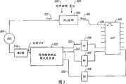
图3是测试系统的方框图,该测试系统通过使用周期微调来产生测试模式信号,并通过使用基于PLL的有程序可控频率范围的时钟来产生时钟信号,能改进边缘布局的精度,还能向DUT时钟输入提供具有低的周期到周期抖动的时钟信号。Figure 3 is a block diagram of a test system that can improve the accuracy of edge placement by using period trimming to generate test pattern signals and by using a PLL-based clock with a programmable frequency range to generate clock signals. The DUT clock input provides a clock signal with low cycle-to-cycle jitter.
系统振荡器(OSC)300通过输入信号Fref 352向锁相环时钟(PLL Clock)提供时钟信号。系统振荡器300还向被2除的电路318提供时钟信号,电路318把时钟信号分频成一半。在这种特定的情况下,系统振荡器300以800MHz运行,但也可以使用其他频率,依赖于应用和设计参数。被2除电路318的输出是主时钟(Clock)414,在本情况下,主时钟414以400MHz运行,但通过用不同频率运行的系统振荡器,或使用其值与应用及设计参数相关联的程序可控分频器,代替被2除电路318,能够获得其他的主时钟频率。时钟414被传送至周期微调测试模式发生器320,模式发生器320有输入/输出线322,与DUT 340特定引脚分开的引脚电子电路336耦合。周期微调测试模式发生器320通过输入/输出线322,向引脚电子电路336提供测试模式信号,该引脚电子电路336接着提供给DUT 340的数据引脚。如上面所指出,PLL时钟360接收通过信号Fref 352的系统振荡器信号,还接收软件控制信号(SW Control)306及复位信号(Reset)308。PLL时钟360最多能够向每侧四条时钟引脚提供时钟信号,该四条时钟引脚可以或者用作四个单端时钟或者用作两个微分时钟。当然,与应用和设计参数有关,可以向每侧多于四条时钟引脚提供时钟信号。在本例中,PLL时钟360向时钟输入338提供单个时钟信号。The system oscillator (OSC) 300 provides a clock signal to a phase locked loop clock (PLL Clock) through an
在本例中,Fref 352的频率是800MHz,但与应用和设计参数有关,通过使用例如有不同频率的系统振荡器,能够获得其他的频率。PLL时钟360输出PLL时钟信号(Fout)380,该PLL时钟信号(Fout)与发送至DUT 340数据引脚的测试模式信号,频率相似且相位匹配。如上面所指出,频率相似意味着信号Fout 380是测试模式信号的倍数或约数。DUT 340的时钟输入338,从PLL时钟360接收信号Fout 380。In this example, the frequency of
如图3所示,PLL时钟360与周期微调测试模式发生器320的结合,特别适合诸如结构测试的应用,该种应用可以利用微调技术的灵活性,向DUT 340数据引脚提供测试数据,并向DUT 340提供PLL技术的低周期到周期抖动的时钟输入。例如,在结构测试中,由于下面指出的理由,DUT 340的内部时钟,必须与有低的周期到周期抖动的测试系统时钟精确同步。As shown in FIG. 3, the combination of
因为大多数高速集成电路装置,是由内部PLL时钟驱动的,DUT 340的内部PLL时钟,把测试系统提供的时钟信号,与时钟输入338相乘(例如,在常规系统中,是基于微调的时钟信号,而在本实施例中,就是信号Fout 380),以便按高的频率运行DUT 340的核心。例如,100MHz的测试系统的时钟输入,可以与DUT的内部PLL时钟相乘,获得1.6GHz的核心运行。在把测试模式信号加到DUT 340的数据引脚之后,DUT 340数据引脚的状态被仔细审查,并与预期结果比较。因为DUT 340的核心以1.6GHz运行(即周期为625ps),在向时钟输入338提供的时钟信号中,任何周期到周期的抖动,例如在基于微调的时钟中20ps的抖动,会对DUT的内部PLL时钟的运行,产生不利影响。结果能导致抖动的核心时钟,而抖动的核心时钟最后降低DUT的定时性能并可能影响测试的出产量。Since most high-speed integrated circuit devices are driven by an internal PLL clock, the internal PLL clock of the
但是,在本实施例中,提供给DUT 340的是稳定的时钟信号Fout 380,就是说,它有较低的周期到周期的抖动(如2ps),在具有亚纳秒内部核心时钟的应用中,这样的抖动不会冲蚀定时界限。还有,可以使信号Fout 380与发送至DUT 340数据引脚的测试模式信号频率相似且相位匹配。而且,在各优点当中,PLL时钟360与常规的基于微调的时钟提供的边缘布局精度相比,能改进边缘布局的精度。However, in this embodiment, the
图4画出周期微调测试模式发生器320的方框图。全局定序器412接收主时钟(Clock)414。全局定序器412,或者可以用本文引用的U.S.Pat.Nos.5,477,139和5,212,443中公开的全局定序器,或者可以用产生能用于产生测试周期的相似输出信号的其他全局定序器。在图4所示的例子中,主时钟414以400MHz运行,基本周期是2.5ns。FIG. 4 shows a block diagram of the cycle trimming
全局定序器412输出主时钟414和时间零信号416。时间零信号416是专用的时钟脉冲缘,测试周期以它作参考。全局定序器412使用微调技术,在线418上提供许多数字比特,为测试周期的开始指示离开时间零信号416的偏移,该种微调技术例如是U.S.Pat.No.5,477,139中公开的一种微调技术,本文引用该专利。该偏移被称为周期微调或周期偏移。周期微调值可以由主时钟周期的整数加上主时钟的分数部分合成。该分数部分,连同测试周期的周期分辨率,可以由例如传送8比特信息来提供。使用周期微调,可以给出提供测试周期分辨率的能力,该周期分辨率不限于主时钟414的周期分辨率。在本例中,400MHz的主时钟周期分辨率,是9.765625ps(即2.5ns被256除)。Global sequencer 412 outputs master clock 414 and time zero signal 416 . Time zero signal 416 is the dedicated clock edge to which the test cycle is referenced. Global sequencer 412 uses a trimming technique, such as the one disclosed in U.S. Pat. technology, the patent is cited herein. This offset is known as cycle trim or cycle offset. The period trim value can be synthesized by adding the integer number of the period of the main clock to the fractional part of the main clock. This fractional part, together with the cycle resolution of the test cycle, can be provided by, for example, transmitting 8 bits of information. Using period trimming, the ability to provide test period resolution that is not limited to the period resolution of master clock 414 may be given. In this example, the period resolution of the master clock of 400MHz is 9.765625ps (that is, 2.5ns divided by 256).
所有这些信号都向许多局部定序器420提供,局部定序器可以使用公开在U.S.Pat.Nos.6,128,754,5,477,139,和5,212,443中的局部定序器,本文引用这些专利,也可以使用本领域一般人员熟知的任何其他局部定序器。局部定序器420产生测试模式信号,该测试模式信号包括事件模式,如各1和各0,以及每一事件出现的时间(即测试周期),该时间以主时钟414、时间零信号416、和周期微调值为基础。每一局部定序器有输入/输出线322,与分开的引脚电子电路336耦合,该引脚电子电路336一般用同轴电缆连接至局部定序器420。All of these signals are provided to a number of local sequencers 420, which may use the local sequencers disclosed in U.S. Pat. Nos. Any other local sequencer known to the personnel. Partial sequencer 420 produces test mode signal, and this test mode signal comprises event pattern, as each 1 and each 0, and the time (i.e. test cycle) that each event occurs, and this time is represented by master clock 414, time zero signal 416, and Period Trim values are based on. Each local sequencer has input/
图5画出PLL时钟360的方框图,它能在具有程序可控频率范围的Fout 380上产生时钟信号。此外,在Fout 380上的时钟信号,可以与周期微调测试模式信号发生器320产生的测试模式信号频率相似且相位匹配。而且,如上所述,PLL时钟360能够获得改进的边缘布局精度,还能够在具有低周期到周期抖动的Fout 380上,提供时钟信号。FIG. 5 shows a block diagram of
PLL时钟360接收参考信号(Fref)352,该参考信号352经程序可控的除以M电路520处理。得到的信号(Fref/M)518由乘法器524接收,乘法器524还从程序可控的除以N电路530接收反馈信号529。得到的信号525被发送至低通滤波器526。滤波后的信号被发送至压控振荡器(VCO)528。VCO(VCO out)的输出542,被反馈至程序可控的除以N电路530和发送至被2除电路532及程序可控的除以D电路534,除以D电路534在Fout 380上输出时钟信号,该时钟信号与周期微调测试模式信号发生器320产生的测试模式信号,频率相似且相位匹配。通过使用复位信号(Reset)308和SWControl 306,可以实现频率合成和相位匹配,SW Control 306利用延迟线(DL)522和门526,提供软件校准的定时延迟。频率合成和相位匹配,下面还要更详细解释。
频率合成frequency synthesis
PLL时钟360接收信号Fref 352,信号Fref 352在本例中的周期为1.25ns(即800MHz),但与应用和设计参数有关,也可以用其他的频率。信号Fout 380的频率,可按方程式(1)计算:The
这里Fref是参考时钟信号频率,N和M是程序可控系数,及D是程序可控分频器534的程序可控系数,D可以是1、2、4、8、16或32,或2的任何乘方,与应用和设计参数有关。信号Fout 380的周期,可按方程式(2)计算:Here Fref is the reference clock signal frequency, N and M are the program controllable coefficients, and D is the program controllable coefficient of the program controllable frequency divider 534, D can be 1, 2, 4, 8, 16 or 32, or Any power of 2, depending on application and design parameters. The period of
方程式(2)表明,PLL时钟360的周期分辨率,依赖于N的值,而周期的持续时间(即频率范围)则受M和D值的影响。在本实施例中,最小的要求PLL时钟360的周期分辨率是39.0625ps。因为Tref是1.25ns,可以把N设为64和把M和D设为1而获得要求的分辨率。如果PLL时钟360需要不同的周期分辨率,例如,在Tref为1.25ns时,可以把N设为32和把M和D设为1,而获得78.125ps的周期分辨率。在确定PLL时钟360的最小周期分辨率后(如39.0625ps),PLL时钟360的频率范围,可以通过设定M和D的系数而确定。Equation (2) shows that the cycle resolution of the
在本实施例中,假定周期微调测试模式发生器320接收的主时钟414正以400MHz运行,则信号Fout 380需要的频率范围是200到400MHz。利用方程式(1),如果Fout 380是400MHz,Fref 352是800MHz,N是64,及D是1,则M系数的值是64。因为对信号Fout 380需要的频率范围,不要求分频,所以把程序可控分频器534的D系数设为1。同样,如果Fout 380是200MHz,Fref 352是800MHz,N是64,及D是1,则M系数的值是128。因此,M系数的值在64到128之间。通过改变程序可控分频器534的D系数,产生宽范围的时钟频率是可能的。表1表明在N固定为64时,可以获得作为M和D的函数的时钟周期。In this embodiment, assuming that the master clock 414 received by the period fine-tuning
从表1可见,通过改变程序可控分频器534的D系数对PLL时钟360的分频,将成正比地影响频率的分辨率。然而,用周期微调测试模式发生器320产生的测试模式信号的频率合成,能够通过给定需要的N而选择适当的M和D来实现。不难看出,能够由PLL时钟360产生的时钟周期,是周期微调测试模式发生器320产生的测试周期的倍数。It can be seen from Table 1 that by changing the D coefficient of the program-controllable frequency divider 534 to divide the frequency of the
D
表1:作为M和D函数的周期,以ps为单位Table 1: Period as a function of M and D in ps
相位对准phase alignment
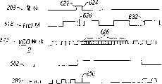
信号Fout 380与测试模式信号的相位对准,可以通过两步处理过程达到:首先,令除以M电路520以适当的校准复位;然后,在来自VCO 526的瞬态已经结束之后,该瞬态发生在复位操作之后,使信号Fout 380与测试模式(该测试模式由周期微调测试模式发生器320产生)相位对准。Phase alignment of
在每个分频器520、532、534上,相位信息丢失(反馈的除以N电路530除外,因为该电路与来自VCO的(VCO out)542相乘)。通常都会发生相位信息丢失,除非除以M电路520在每次测试开始时被精确复位。使除以M电路520复位,可以使用复位信号(Reset)308完成。能够用软件控制的延迟线DL 522,补偿产生复位信号308的复位逻辑中任何延迟,从而保证在恰当的时间向除以M电路530提供复位信号308。定时校准或定时延迟值,通过信号SW Control 306引入DL 522。At each divider 520, 532, 534, phase information is lost (except for the feedback divide-by-N circuit 530, which multiplies (VCO out) 542 from the VCO). Loss of phase information typically occurs unless divide-by-M circuit 520 is reset precisely at the beginning of each test. Resetting divide-by-M circuit 520 may be accomplished using reset signal (Reset) 308 . Any delay in the reset logic that generates
在来自VCO 526的瞬态已经结束之后,PLL时钟360的输出与测试模式的相位对准,能够通过相位比较器(未画出)完成。如上所述,因为一般需要归零且可重复的信号Fout 380,所以必须屏蔽该瞬态。这一点可以用门536产生的门信号582完成。门信号582通过使用复位信号308和定时校准或定时延迟值,与信号Fref/M 518和信号Fout 380同步,该定时校准或定时延迟值是通过信号SW Control 306引入门536的。一旦已经对特定频率确定了定时校准,就能够计算所有其他频率。本领域一般人员知道,如何用熟知的技术计算这些其他频率。After the transient from VCO 526 has ended, phase alignment of the output of
图6画出Fout 380复位的定时,以获得与复位信号308的固定时间关系,复位信号308接着又与周期微调测试模式发生器320产生的测试模式相位对准。不难看出,在复位信号的上升缘622,信号Fref/M 518驱动至低态628。信号Fref/M 518一直维持在低态628,直至复位信号的下降缘624。此外,在复位信号的上升缘622,门信号582被驱动至高态626,该高态626驱动信号Fout 380至低态630。门信号582维持在高态626,至少到信号VCOout/2543中的瞬态620结束,此后,门信号582与信号Fout 380同步地驱动至的低态。结果,测试模式与信号Fout 380相位对准。FIG. 6 illustrates the timing of the reset of
前述的实施例,把基于周期微调测试模式信号发生器的灵活性,与基于PLL时钟的低周期到周期抖动结合。该种结合向DUT提供稳定的时钟,该稳定的时钟在具有亚纳秒内部核心时钟的应用中,不会冲蚀定时界限。The foregoing embodiments combine the flexibility of cycle-based fine-tuning of the test pattern signal generator with low cycle-to-cycle jitter based on the PLL clock. This combination provides a stable clock to the DUT that does not erode timing boundaries in applications with sub-nanosecond internal core clocks.
本文说明的计算方面,可以在数字电子电路中实现,或在计算机硬件、固件、软件、或它们的组合中实现。只要合适,这些系统和技术方面,能够用有形地体现在机器可读存储装置中的计算机程序产品来实现,供可编程处理器执行;而方法的步骤,能够用执行指令程序的可编程处理器完成,该指令程序通过对输入数据的操作及产生输出来完成这些功能。The computing aspects described herein can be implemented in digital electronic circuitry, or in computer hardware, firmware, software, or a combination thereof. Where appropriate, these systems and technical aspects can be implemented by a computer program product tangibly embodied in a machine-readable storage device for execution by a programmable processor; and the steps of the methods can be implemented by a programmable processor executing a program of instructions Completion, the instruction program performs these functions by operating on input data and generating output.
为向用户提供人机对话,使用的计算机系统可以有显示装置,如监控器或液晶屏,以便向用户显示信息,以及键盘和指针指针,如鼠标或跟踪球,用户能够通过这些装置向计算机系统输入。可以对计算机编程,以提供图形用户界面,计算机程序通过该用户界面与用户对话。In order to provide the user with man-machine dialogue, the computer system used may have a display device, such as a monitor or LCD screen, to display information to the user, as well as a keyboard and a pointer, such as a mouse or trackball, through which the user can communicate with the computer system. enter. The computer can be programmed to provide a graphical user interface through which the computer program talks to the user.
其他的实施例包括在下述权利要求书之内。Other embodiments are within the following claims.
Claims (36)
Applications Claiming Priority (4)
| Application Number | Priority Date | Filing Date | Title |
|---|---|---|---|
| US27767501P | 2001-03-20 | 2001-03-20 | |
| US60/277,675 | 2001-03-20 | ||
| US27779501P | 2001-03-21 | 2001-03-21 | |
| US60/277,795 | 2001-03-21 |
Publications (1)
| Publication Number | Publication Date |
|---|---|
| CN1527948Atrue CN1527948A (en) | 2004-09-08 |
Family
ID=26958642
Family Applications (1)
| Application Number | Title | Priority Date | Filing Date |
|---|---|---|---|
| CNA028069587APendingCN1527948A (en) | 2001-03-20 | 2002-03-19 | Low jitter clock for test system |
Country Status (7)
| Country | Link |
|---|---|
| US (2) | US7093177B2 (en) |
| EP (2) | EP1377840A2 (en) |
| CN (1) | CN1527948A (en) |
| AU (2) | AU2002245706A1 (en) |
| DE (1) | DE60204556D1 (en) |
| TW (2) | TWI243247B (en) |
| WO (2) | WO2002075336A2 (en) |
Cited By (3)
| Publication number | Priority date | Publication date | Assignee | Title |
|---|---|---|---|---|
| CN1992087B (en)* | 2005-12-28 | 2010-10-06 | 三星电子株式会社 | Parts testing device and method and interface apparatus thereof |
| CN103116124A (en)* | 2011-11-17 | 2013-05-22 | 国民技术股份有限公司 | Chip capable of self-calibration of interior crystal oscillator, calibration system and calibration method |
| CN106855608A (en)* | 2015-12-09 | 2017-06-16 | 深圳市盛德金科技有限公司 | Doubleclocking test circuit |
Families Citing this family (31)
| Publication number | Priority date | Publication date | Assignee | Title |
|---|---|---|---|---|
| US20030160826A1 (en)* | 2002-02-26 | 2003-08-28 | Sun Microsystems, Inc. | Method, apparatus and computer product to organize data on a display and facilitate testing of an integrated circuit design |
| US7313739B2 (en)* | 2002-12-31 | 2007-12-25 | Analog Devices, Inc. | Method and apparatus for testing embedded cores |
| US7392442B2 (en)* | 2003-03-20 | 2008-06-24 | Qualcomm Incorporated | Built-in self-test (BIST) architecture having distributed interpretation and generalized command protocol |
| US7184915B2 (en)* | 2003-03-20 | 2007-02-27 | Qualcomm, Incorporated | Tiered built-in self-test (BIST) architecture for testing distributed memory modules |
| JP4332392B2 (en)* | 2003-09-12 | 2009-09-16 | 株式会社アドバンテスト | Test equipment |
| US7117415B2 (en)* | 2004-01-15 | 2006-10-03 | International Business Machines Corporation | Automated BIST test pattern sequence generator software system and method |
| US7246025B2 (en)* | 2004-01-28 | 2007-07-17 | Texas Instruments Incorporated | Method and apparatus for synchronizing signals in a testing system |
| KR100594240B1 (en)* | 2004-01-29 | 2006-06-30 | 삼성전자주식회사 | Panel Drive Driver and Panel Test Method to Generate Panel Test Patterns |
| US6991161B2 (en)* | 2004-06-23 | 2006-01-31 | Paul Pazniokas | Electronic voting apparatus, system and method |
| EP1752779B1 (en)* | 2004-06-24 | 2008-08-06 | Verigy (Singapore) Pte. Ltd. | Per-pin clock synthesis |
| US7664166B2 (en)* | 2004-12-17 | 2010-02-16 | Rambus Inc. | Pleisiochronous repeater system and components thereof |
| US7228446B2 (en)* | 2004-12-21 | 2007-06-05 | Packet Digital | Method and apparatus for on-demand power management |
| US7337335B2 (en)* | 2004-12-21 | 2008-02-26 | Packet Digital | Method and apparatus for on-demand power management |
| US7375569B2 (en)* | 2005-09-21 | 2008-05-20 | Leco Corporation | Last stage synchronizer system |
| US20070080697A1 (en)* | 2005-09-27 | 2007-04-12 | Sony Corporation | Semiconductor device tester pin contact resistance measurement |
| US8542050B2 (en)* | 2005-10-28 | 2013-09-24 | Sony Corporation | Minimized line skew generator |
| US7516385B2 (en)* | 2006-04-28 | 2009-04-07 | Sony Corporation | Test semiconductor device in full frequency with half frequency tester |
| US7449876B2 (en)* | 2006-05-03 | 2008-11-11 | Agilent Technologies, Inc. | Swept-frequency measurements with improved speed using synthetic instruments |
| US7809052B2 (en)* | 2006-07-27 | 2010-10-05 | Cypress Semiconductor Corporation | Test circuit, system, and method for testing one or more circuit components arranged upon a common printed circuit board |
| US7889824B2 (en)* | 2006-09-28 | 2011-02-15 | Intel Corporation | System and method for alignment of clock to data |
| US7577231B2 (en)* | 2007-03-16 | 2009-08-18 | International Business Machines Corporation | Clock multiplier structure for fixed speed testing of integrated circuits |
| US7788564B2 (en)* | 2007-10-12 | 2010-08-31 | Teradyne, Inc. | Adjustable test pattern results latency |
| US8312299B2 (en) | 2008-03-28 | 2012-11-13 | Packet Digital | Method and apparatus for dynamic power management control using serial bus management protocols |
| US7882406B2 (en)* | 2008-05-09 | 2011-02-01 | Lsi Corporation | Built in test controller with a downloadable testing program |
| US8156391B2 (en)* | 2008-05-27 | 2012-04-10 | Lsi Corporation | Data controlling in the MBIST chain architecture |
| US8046643B2 (en)* | 2008-06-09 | 2011-10-25 | Lsi Corporation | Transport subsystem for an MBIST chain architecture |
| KR101214034B1 (en)* | 2008-09-05 | 2012-12-20 | 가부시키가이샤 어드밴티스트 | Testing apparatus and test method |
| US20110099407A1 (en)* | 2009-10-28 | 2011-04-28 | Ati Technologies Ulc | Apparatus for High Speed Data Multiplexing in a Processor |
| WO2015081980A1 (en)* | 2013-12-02 | 2015-06-11 | Advantest Corporation | Instruction provider and method for providing a sequence of instructions, test processor and method for providing a device under test |
| GB2506825B (en)* | 2014-02-12 | 2014-10-15 | Ultrasoc Technologies Ltd | Functional testing of an integrated circuit chip |
| US9268597B2 (en)* | 2014-04-01 | 2016-02-23 | Google Inc. | Incremental parallel processing of data |
Family Cites Families (16)
| Publication number | Priority date | Publication date | Assignee | Title |
|---|---|---|---|---|
| US5212443A (en)* | 1990-09-05 | 1993-05-18 | Schlumberger Technologies, Inc. | Event sequencer for automatic test equipment |
| US5270643A (en)* | 1990-11-28 | 1993-12-14 | Schlumberger Technologies | Pulsed laser photoemission electron-beam probe |
| CA2127192C (en)* | 1993-07-01 | 1999-09-07 | Alan Brent Hussey | Shaping ate bursts, particularly in gallium arsenide |
| US5491673A (en)* | 1994-06-02 | 1996-02-13 | Advantest Corporation | Timing signal generation circuit |
| US5471176A (en)* | 1994-06-07 | 1995-11-28 | Quantum Corporation | Glitchless frequency-adjustable ring oscillator |
| JP3605150B2 (en)* | 1994-08-22 | 2004-12-22 | 株式会社アドバンテスト | Address pattern generator |
| US5535164A (en)* | 1995-03-03 | 1996-07-09 | International Business Machines Corporation | BIST tester for multiple memories |
| US5673275A (en)* | 1995-09-12 | 1997-09-30 | Schlumberger Technology, Inc. | Accelerated mode tester timing |
| US6061815A (en) | 1996-12-09 | 2000-05-09 | Schlumberger Technologies, Inc. | Programming utility register to generate addresses in algorithmic pattern generator |
| US5883905A (en) | 1997-02-18 | 1999-03-16 | Schlumberger Technologies, Inc. | Pattern generator with extended register programming |
| JPH1138100A (en) | 1997-07-18 | 1999-02-12 | Advantest Corp | Semiconductor test device |
| US6128754A (en)* | 1997-11-24 | 2000-10-03 | Schlumberger Technologies, Inc. | Tester having event generation circuit for acquiring waveform by supplying strobe events for waveform acquisition rather than using strobe events specified by the test program |
| US6237021B1 (en)* | 1998-09-25 | 2001-05-22 | Complex Data Technologies, Inc. | Method and apparatus for the efficient processing of data-intensive applications |
| HUP0301274A2 (en)* | 1998-09-30 | 2003-08-28 | Cadence Design Systems | Block based design methodology |
| US6249889B1 (en)* | 1998-10-13 | 2001-06-19 | Advantest Corp. | Method and structure for testing embedded memories |
| US6266750B1 (en)* | 1999-01-15 | 2001-07-24 | Advanced Memory International, Inc. | Variable length pipeline with parallel functional units |
- 2002
- 2002-03-19CNCNA028069587Apatent/CN1527948A/enactivePending
- 2002-03-19TWTW091105225Apatent/TWI243247B/ennot_activeIP Right Cessation
- 2002-03-19EPEP02713881Apatent/EP1377840A2/ennot_activeWithdrawn
- 2002-03-19DEDE60204556Tpatent/DE60204556D1/ennot_activeExpired - Lifetime
- 2002-03-19WOPCT/US2002/008539patent/WO2002075336A2/ennot_activeApplication Discontinuation
- 2002-03-19EPEP02725274Apatent/EP1377841B1/ennot_activeExpired - Lifetime
- 2002-03-19AUAU2002245706Apatent/AU2002245706A1/ennot_activeAbandoned
- 2002-03-19USUS10/102,536patent/US7093177B2/ennot_activeExpired - Fee Related
- 2002-03-19USUS10/102,526patent/US7143326B2/ennot_activeExpired - Fee Related
- 2002-03-19AUAU2002255849Apatent/AU2002255849A1/ennot_activeAbandoned
- 2002-03-19WOPCT/US2002/008627patent/WO2002075337A2/ennot_activeApplication Discontinuation
- 2002-03-19TWTW091105224Apatent/TWI234001B/ennot_activeIP Right Cessation
Cited By (5)
| Publication number | Priority date | Publication date | Assignee | Title |
|---|---|---|---|---|
| CN1992087B (en)* | 2005-12-28 | 2010-10-06 | 三星电子株式会社 | Parts testing device and method and interface apparatus thereof |
| CN103116124A (en)* | 2011-11-17 | 2013-05-22 | 国民技术股份有限公司 | Chip capable of self-calibration of interior crystal oscillator, calibration system and calibration method |
| CN103116124B (en)* | 2011-11-17 | 2016-05-18 | 国民技术股份有限公司 | Can self calibration chip, crystal oscillator calibration test system and the calibration steps of inner crystal oscillator |
| CN106855608A (en)* | 2015-12-09 | 2017-06-16 | 深圳市盛德金科技有限公司 | Doubleclocking test circuit |
| CN106855608B (en)* | 2015-12-09 | 2023-11-14 | 深圳市盛德金科技有限公司 | Dual clock test circuit |
Also Published As
| Publication number | Publication date |
|---|---|
| WO2002075337A2 (en) | 2002-09-26 |
| DE60204556D1 (en) | 2005-07-14 |
| AU2002255849A1 (en) | 2002-10-03 |
| TWI243247B (en) | 2005-11-11 |
| TWI234001B (en) | 2005-06-11 |
| US20030005360A1 (en) | 2003-01-02 |
| WO2002075336A9 (en) | 2004-02-12 |
| AU2002245706A1 (en) | 2002-10-03 |
| WO2002075336A2 (en) | 2002-09-26 |
| US7093177B2 (en) | 2006-08-15 |
| EP1377841B1 (en) | 2005-06-08 |
| WO2002075337A3 (en) | 2003-10-23 |
| US7143326B2 (en) | 2006-11-28 |
| EP1377841A2 (en) | 2004-01-07 |
| EP1377840A2 (en) | 2004-01-07 |
| WO2002075336A3 (en) | 2003-11-06 |
| US20020188902A1 (en) | 2002-12-12 |
Similar Documents
| Publication | Publication Date | Title |
|---|---|---|
| CN1527948A (en) | Low jitter clock for test system | |
| US11381229B2 (en) | Clock spread spectrum circuit, electronic equipment, and clock spread spectrum method | |
| JP2976206B2 (en) | Apparatus for processing data at a controlled rate in response to a periodic reference signal input to produce an accurately time-controlled output signal | |
| EP1151312B1 (en) | Analog clock module | |
| US10686458B1 (en) | Method and apparatus for improving frequency source frequency accuracy and frequency stability | |
| US20090051347A1 (en) | High frequency delay circuit and test apparatus | |
| CN1302477A (en) | Clock generation circuit, serial/parallel converter and parallel/serial converter and semiconductor device | |
| Szplet et al. | A 45 ps time digitizer with a two-phase clock and dual-edge two-stage interpolation in a field programmable gate array device | |
| US8392145B2 (en) | Timing generator | |
| KR100464933B1 (en) | Fully digital clock synthesizer | |
| US11012080B2 (en) | Frequency locked loop, electronic device, and frequency generation method | |
| El-Shennawy et al. | Fractional-N PLL optimization for highly linear wideband chirp generation for FMCW radars | |
| CN112787638B (en) | Dual-channel synchronous reload pulse generation method | |
| US7525351B2 (en) | Fixed frequency clock output having a variable high frequency input clock and an unrelated fixed frequency reference signal | |
| US20060087346A1 (en) | Phase difference detecting apparatus | |
| JP2002529744A (en) | Analog clock module | |
| US7072920B2 (en) | Method and apparatus for digital frequency conversion | |
| US8994422B2 (en) | Use of Frequency addition in a PLL control loop | |
| JP2000249747A (en) | Timing signal generating circuit for semiconductor test device | |
| US8575973B1 (en) | Frequency synthesizer with zero deterministic jitter | |
| US20090009220A1 (en) | Signal generating apparatus, periodic-signal observing system, integrated circuit, periodic-signal observing method, and method of testing integrated circuit | |
| JP2543514B2 (en) | Timing signal generator | |
| CN119311145A (en) | Duty cycle correction device for large touch and display driver integrated systems |
Legal Events
| Date | Code | Title | Description |
|---|---|---|---|
| C06 | Publication | ||
| PB01 | Publication | ||
| C10 | Entry into substantive examination | ||
| SE01 | Entry into force of request for substantive examination | ||
| ASS | Succession or assignment of patent right | Owner name:INTEGRITY SYSTEM CO., LTD. Free format text:FORMER OWNER: NEPETEST INC. Effective date:20060210 | |
| C41 | Transfer of patent application or patent right or utility model | ||
| TA01 | Transfer of patent application right | Effective date of registration:20060210 Address after:American California Applicant after:Nepetest Corp. Address before:American California Applicant before:Nptest Inc. | |
| C02 | Deemed withdrawal of patent application after publication (patent law 2001) | ||
| WD01 | Invention patent application deemed withdrawn after publication |