CN1509982A - A carbon nanotube array structure and its growth method - Google Patents
A carbon nanotube array structure and its growth methodDownload PDFInfo
- Publication number
- CN1509982A CN1509982ACNA021497265ACN02149726ACN1509982ACN 1509982 ACN1509982 ACN 1509982ACN A021497265 ACNA021497265 ACN A021497265ACN 02149726 ACN02149726 ACN 02149726ACN 1509982 ACN1509982 ACN 1509982A
- Authority
- CN
- China
- Prior art keywords
- carbon nano
- catalyst
- carbon
- nano tube
- carbon nanotube
- Prior art date
- Legal status (The legal status is an assumption and is not a legal conclusion. Google has not performed a legal analysis and makes no representation as to the accuracy of the status listed.)
- Granted
Links
Images


Classifications
- D—TEXTILES; PAPER
- D01—NATURAL OR MAN-MADE THREADS OR FIBRES; SPINNING
- D01F—CHEMICAL FEATURES IN THE MANUFACTURE OF ARTIFICIAL FILAMENTS, THREADS, FIBRES, BRISTLES OR RIBBONS; APPARATUS SPECIALLY ADAPTED FOR THE MANUFACTURE OF CARBON FILAMENTS
- D01F9/00—Artificial filaments or the like of other substances; Manufacture thereof; Apparatus specially adapted for the manufacture of carbon filaments
- D01F9/08—Artificial filaments or the like of other substances; Manufacture thereof; Apparatus specially adapted for the manufacture of carbon filaments of inorganic material
- D01F9/12—Carbon filaments; Apparatus specially adapted for the manufacture thereof
- D01F9/127—Carbon filaments; Apparatus specially adapted for the manufacture thereof by thermal decomposition of hydrocarbon gases or vapours or other carbon-containing compounds in the form of gas or vapour, e.g. carbon monoxide, alcohols
- B—PERFORMING OPERATIONS; TRANSPORTING
- B82—NANOTECHNOLOGY
- B82Y—SPECIFIC USES OR APPLICATIONS OF NANOSTRUCTURES; MEASUREMENT OR ANALYSIS OF NANOSTRUCTURES; MANUFACTURE OR TREATMENT OF NANOSTRUCTURES
- B82Y30/00—Nanotechnology for materials or surface science, e.g. nanocomposites
- B—PERFORMING OPERATIONS; TRANSPORTING
- B82—NANOTECHNOLOGY
- B82Y—SPECIFIC USES OR APPLICATIONS OF NANOSTRUCTURES; MEASUREMENT OR ANALYSIS OF NANOSTRUCTURES; MANUFACTURE OR TREATMENT OF NANOSTRUCTURES
- B82Y10/00—Nanotechnology for information processing, storage or transmission, e.g. quantum computing or single electron logic
- Y—GENERAL TAGGING OF NEW TECHNOLOGICAL DEVELOPMENTS; GENERAL TAGGING OF CROSS-SECTIONAL TECHNOLOGIES SPANNING OVER SEVERAL SECTIONS OF THE IPC; TECHNICAL SUBJECTS COVERED BY FORMER USPC CROSS-REFERENCE ART COLLECTIONS [XRACs] AND DIGESTS
- Y10—TECHNICAL SUBJECTS COVERED BY FORMER USPC
- Y10T—TECHNICAL SUBJECTS COVERED BY FORMER US CLASSIFICATION
- Y10T428/00—Stock material or miscellaneous articles
- Y10T428/30—Self-sustaining carbon mass or layer with impregnant or other layer
Landscapes
- Engineering & Computer Science (AREA)
- Chemical & Material Sciences (AREA)
- Nanotechnology (AREA)
- Physics & Mathematics (AREA)
- Textile Engineering (AREA)
- General Chemical & Material Sciences (AREA)
- Chemical Kinetics & Catalysis (AREA)
- Composite Materials (AREA)
- Condensed Matter Physics & Semiconductors (AREA)
- General Physics & Mathematics (AREA)
- Materials Engineering (AREA)
- Crystallography & Structural Chemistry (AREA)
- Thermal Sciences (AREA)
- Carbon And Carbon Compounds (AREA)
- Catalysts (AREA)
Abstract
Translated fromChineseDescription
Translated fromChinese【技术领域】【Technical field】
本发明关于一种碳纳米管阵列结构及其生长方法。The invention relates to a carbon nanotube array structure and a growth method thereof.
【背景技术】【Background technique】
由于碳纳米管独特的电学性质,其在纳米集成电路、单分子器件等领域的应用有着不可估量的前景。目前人们已经能够在实验室里少量制造基于碳纳米管的场效应管、逻辑器件及存储器件等,并研究了它的性质,具体请参阅Sander J Tans等人1998年发表在Nature 393-49,Room-temperature transistorbased on a single carbon nanotube一文。但大规模的制备和具有实际意义的应用则必须求助于由下而上(Bottom Up)的制备工艺。Due to the unique electrical properties of carbon nanotubes, their applications in the fields of nano-integrated circuits and single-molecule devices have immeasurable prospects. At present, people have been able to manufacture a small amount of carbon nanotube-based field effect transistors, logic devices, and storage devices in the laboratory, and have studied its properties. For details, please refer to Sander J Tans et al. published in Nature 393-49 in 1998, Room-temperature transistor based on a single carbon nanotube article. However, large-scale preparation and practical application must resort to the bottom-up (Bottom Up) preparation process.
由下而上的制备工艺要求能够对碳纳米管的生长位置、方向、大小、长短、甚至碳纳米管的螺旋度进行必要的控制,通过少量而经济的步骤直接生长出所需要的器件结构。范守善等人在Science 283,512-514(1999),Self-oriented regular arrays of carbon nanotubes and their field emissionproperties一文中,以及Z.F.Ren等人在Science 282,1105-1107(Nov 6,1998),Synthesis of large arrays of well-aligned carbon nanotubes on glass一文中均揭露了一种通过催化剂图形(Patterned Catalyst)来控制碳纳米管的生长位置及使其垂直于基底的生长方法。The bottom-up preparation process requires the ability to control the growth position, direction, size, length, and even the helicity of carbon nanotubes, and directly grow the required device structure through a small number of economical steps. Fan Shoushan et al. in Science 283, 512-514 (1999), Self-oriented regular arrays of carbon nanotubes and their field emission properties, and Z.F.Ren et al. in Science 282, 1105-1107 (Nov 6, 1998), Synthesis of Large arrays of well-aligned carbon nanotubes on glass all disclose a method of controlling the growth position of carbon nanotubes and making them perpendicular to the substrate through the catalyst pattern (Patterned Catalyst).
另外,B.Q.Wei等人在Nature 416,495-496(Apr 4,2002),Organizedassembly of carbon nanotubes一文中揭露了一种可以通过对基底形状的设计实现碳纳米管在三维基底上生长出垂直于各处表面的生长方法。In addition, B.Q.Wei et al disclosed in Nature 416, 495-496 (Apr 4, 2002), Organized assembly of carbon nanotubes that a carbon nanotube can be grown on a three-dimensional substrate perpendicular to each The method of growth on the surface.
但是上述方法中所获得的碳纳米管阵列均垂直于生长的基底,无法对阵列的生长方向做出控制和改变。However, the carbon nanotube arrays obtained in the above method are all perpendicular to the growth substrate, and the growth direction of the array cannot be controlled and changed.
Yuegang Zhang等人在Applied Physics Letters,Vol.79,Number 19,Nov 5,2001,Electric-field-directed growth of aligned single-walled carbon nanotubes一文中揭露了一种通过电场控制碳纳米管的生长方向的方法,在电场的作用下,可控制碳纳米管沿电场方向生长。Yuegang Zhang et al disclosed a method of controlling the growth direction of carbon nanotubes by electric field in Applied Physics Letters, Vol.79, Number 19, Nov 5, 2001, Electric-field-directed growth of aligned single-walled carbon nanotubes The method can control the growth of carbon nanotubes along the direction of the electric field under the action of the electric field.
但是上述方法中,用电场控制碳纳米管生长方向的方法则会加重器件设计的复杂程度,而且由于电场本身的广域性,难以实现对局部多种生长方向的控制。这些因素都限制了碳纳米管器件设计的多样化和实用性,因此,发明一种不需外场的局部碳纳米管生长方向控制方法实为必要。However, in the above methods, the method of controlling the growth direction of carbon nanotubes with an electric field will increase the complexity of device design, and due to the wide-area nature of the electric field itself, it is difficult to achieve local control of multiple growth directions. These factors limit the diversification and practicability of carbon nanotube device design. Therefore, it is necessary to develop a local carbon nanotube growth direction control method that does not require an external field.
【发明内容】【Content of invention】
本发明要解决的一个技术问题是提供一种向一特定方向弯曲的碳纳米管阵列结构。A technical problem to be solved by the present invention is to provide a carbon nanotube array structure bent in a specific direction.
本发明解决的另一个技术问题是提供一种生长上述碳纳米管阵列的方法。Another technical problem solved by the present invention is to provide a method for growing the above-mentioned carbon nanotube array.
为解决上述技术问题,本发明揭示一种碳纳米管阵列结构,包括一基底、形成于基底上的催化剂合金颗粒及从催化剂合金颗粒上长出的碳纳米管阵列,该催化剂合金颗粒中包括至少两种影响碳纳米管长生速度的调节材料,该调节材料沿一特定方向分布,该碳纳米管阵列向该特定方向弯曲In order to solve the above technical problems, the present invention discloses a carbon nanotube array structure, including a substrate, catalyst alloy particles formed on the substrate and carbon nanotube arrays grown from the catalyst alloy particles, the catalyst alloy particles include at least Two kinds of adjustment materials that affect the growth rate of carbon nanotubes, the adjustment materials are distributed along a specific direction, and the carbon nanotube array is bent to the specific direction
本发明同时还揭示生长上述碳纳米管阵列的方法,其步骤包括:The present invention also discloses a method for growing the above-mentioned carbon nanotube array, the steps of which include:
(1)提供一基底;(1) provide a base;
(2)在基底的表面沉积一催化剂层;(2) depositing a catalyst layer on the surface of the substrate;
(3)在催化剂层上沉积至少两种影响碳纳米管生长速度的调节材料;(3) Depositing at least two adjustment materials that affect the growth rate of carbon nanotubes on the catalyst layer;
(4)在含氧气氛中退火,使催化剂层氧化成为催化剂颗粒;(4) annealing in an oxygen-containing atmosphere to oxidize the catalyst layer into catalyst particles;
(5)通入碳源气,生长碳纳米管。(5) Introducing carbon source gas to grow carbon nanotubes.
现有技术中碳纳米管阵列均是线性生长,本发明提供的碳纳米管阵列向一预定的方向弯曲,丰富了碳纳米管器件设计的多样性,为碳纳米管器件的设计提供了更多的选择空间。In the prior art, carbon nanotube arrays all grow linearly. The carbon nanotube arrays provided by the present invention are bent in a predetermined direction, which enriches the diversity of carbon nanotube device designs and provides more possibilities for the design of carbon nanotube devices. choice space.
与现有的碳纳米管阵列的生长方法相比较,本发明提供的方法是在催化剂层上沉积影响碳纳米管长生速度的调节材料,通过控制调节材料在不同位置的种类与分布,实现基底的不同位置碳纳米管有不同的长生速度,因碳纳米管之间存在范德华兹力(Van Der Waals Force),使得碳纳米管阵列在生长过程中受其影响向一特定方向弯曲,其中影响碳纳米管长生速度的调节材料的种类和分布的调制是决定催化剂层上碳纳米管阵列弯曲状况的主要因素。Compared with the existing growth methods of carbon nanotube arrays, the method provided by the present invention is to deposit an adjustment material that affects the growth rate of carbon nanotubes on the catalyst layer, and realize the growth of the substrate by controlling the type and distribution of the adjustment material at different positions. Carbon nanotubes at different positions have different growth rates, because there is Van Der Waals Force (Van Der Waals Force) between carbon nanotubes, so that the carbon nanotube array is bent in a specific direction during the growth process, which affects the carbon nanotubes. Adjustment of tube growth rate The modulation of the type and distribution of materials is the main factor determining the bending state of the carbon nanotube array on the catalyst layer.
【附图说明】【Description of drawings】
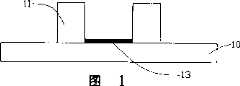
图1是本发明中沉积有催化剂层的基底示意图。Fig. 1 is a schematic diagram of a substrate deposited with a catalyst layer in the present invention.
图2是图1所示催化剂层一侧上沉积一种调节材料的示意图。Fig. 2 is a schematic diagram of depositing a conditioning material on one side of the catalyst layer shown in Fig. 1 .
图3是在图2沉积的基础上在催化剂层的另一侧沉积另一种调节材料示意图。FIG. 3 is a schematic diagram of depositing another regulating material on the other side of the catalyst layer based on the deposition in FIG. 2 .
图4是图3所示的催化剂层与调节材料所形成催化剂合金颗粒的示意图。FIG. 4 is a schematic diagram of catalyst alloy particles formed by the catalyst layer and the adjusting material shown in FIG. 3 .
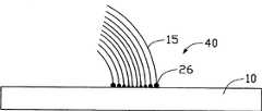
图5是图4所示的催化剂合金颗粒上长出的碳纳米管阵列示意图。FIG. 5 is a schematic diagram of carbon nanotube arrays grown on the catalyst alloy particles shown in FIG. 4 .
图6是本发明两种调节材料沉积的另一分布示意图。Fig. 6 is another schematic diagram of the deposition of two regulating materials according to the present invention.
图7是本发明沉积两种调节材料过程的又一示意图。Fig. 7 is another schematic diagram of the process of depositing two regulating materials according to the present invention.
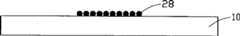
图8是图7所示的催化剂层与调节材料所形成的催化剂合金颗粒示意图。FIG. 8 is a schematic diagram of catalyst alloy particles formed by the catalyst layer and the adjusting material shown in FIG. 7 .
图9是图8所示的催化剂合金颗粒上长出的碳纳米管阵列示意图。FIG. 9 is a schematic diagram of carbon nanotube arrays grown on the catalyst alloy particles shown in FIG. 8 .
图10是本发明沉积多种调节材料的过程示意图。Fig. 10 is a schematic diagram of the process of depositing various conditioning materials according to the present invention.
【具体实施方式】【Detailed ways】
请参阅图1,首先提供一基底10,该基底10选用硅,在该基底10上形成一光阻11,通过光刻使光阻11形成预定的图案。在需要生长碳纳米管的位置沉积数纳米厚的催化剂13,催化剂13的沉积方法可选用热蒸发沉积法、也可选用电子束加热蒸发法等方法配合光刻工艺或图形掩模完成,催化剂13的厚度至少为2~3纳米,至多为10纳米,且厚度需均匀一致,其材料可选用铁、钴、镍或其合金,本实施方式一选用铁作为催化剂13的材料,其沉积的厚度为6纳米。Referring to FIG. 1 , firstly, a
请参阅图2,在催化剂13一侧沉积一层影响碳纳米管生长速度的调节材料221,该调节材料221的厚度由一端向另一端逐渐减薄,一般要求较厚端的厚度不超出10纳米,较薄一端的厚度可接近零纳米,本实施方式是通过在光阻11的斜上方放置一掩模板18,在该掩模板18的上方一定距离处放置一直线型蒸发源22,该掩膜板18端部181与该直线型蒸发源22的端部225平齐,通过热蒸发沉积法,在催化剂13的一侧沉积一层厚度渐变的调节材料221,所沉积的调节材料221较厚端的厚度为8纳米,较薄一端的厚度为零纳米,本实施方式一所用的调节材料221材质是金属钼,该材料在碳纳米管生长过程中具有加快碳纳米管生长速度的特性。Referring to Fig. 2, a layer of regulating
请配合参阅图3,将掩模板18移至调节材料221的正上方,在掩模板18的上方一定距离处放置一直线型蒸发源24,掩膜板18的端部181和该直线型蒸发源24的端部245及调节材料221较薄端在垂直方向上平齐,利用与沉积调节材料221相同的沉积方法,在催化剂13的另一侧沉积一层调节材料241,调节材料241较厚的一端的厚度也为8纳米,较薄一端的厚度为零纳米,其厚度变化方向与调节材料221厚度变化方向相反,其较薄端与调节材料221较薄端相接,本实施方式中调节材料241所用的材质是金属铜,该材料在碳纳米管生长过程中具有减缓碳纳米管生长速度的特性。Please refer to FIG. 3 , move the
上述直线型蒸发源22和24可用沿直线移动的点蒸发源来代替,调节材料221和调节材料241的沉积方法也可以选用其它的方法替代,如电子束蒸发等有方向性的沉积方法配合光刻工艺或图形掩模完成,或者利用溶液喷涂配合甩膜、光刻等工艺完成。The above-mentioned
请一并参阅图3和图4,洗除光阻11,将沉积有催化剂13及调节材料221及调节材料241的基底10置于空气中,在200℃~400℃下退火,使催化剂13氧化,收缩成为纳米级的催化剂颗粒(图未示),氧化时间的长短与氧化时的温度催化剂的种类有关,温度越高,相对的氧化时间越短。再将基底10置于反应炉(图未示)中,在保护气体氩气的保护下,通入碳源气乙炔,利用热化学气相沉积法,在600~700℃下生长10分钟,此时催化剂铁与调节材料221和调节材料241形成催化剂合金颗粒26,如图4所示,其中,调节材料221与调节材料241较厚一端催化剂合金颗粒26较大,调节材料221与调节材料241的含量较高,调节材料221与调节材料241较薄一端催化剂合金颗粒26较小,调节材料221与调节材料241的含量相对较低,调节材料221较厚一端催化剂合金颗粒26中钼的含量最多,又因调节材料221钼具有加快碳纳米管生长速度的特性,碳纳米管的生长受钼影响最大,因而生长最快,相反,调节材料241较厚一端催化剂合金颗粒26中铜的含量最多,铜具有减缓碳纳米管生长速度的特性,故生长速度最慢,而中间的催化剂合金颗粒26中调节材料221与调节材料241的含量渐变,因而,受其影响的碳纳米管的生长速度也渐变,故,在上述催化剂合金颗粒26上生长出的碳纳米管阵列15(参阅图5)向调节材料241较厚一侧弯曲,即向生长速度最慢的一端弯曲。Please refer to FIG. 3 and FIG. 4 together, wash off the
碳纳米管生长的碳源气也可以选用含碳的其它气体,如乙烯等,保护气体也可为其它气体,如氮气、氢气等。控制生长时间和生长温度则可以控制碳纳米管阵列15的生长高度。The carbon source gas for carbon nanotube growth can also be selected from other carbon-containing gases, such as ethylene, and the protective gas can also be other gases, such as nitrogen, hydrogen, etc. Controlling the growth time and temperature can control the growth height of the
请参阅图5,利用上述方法获得的碳纳米管阵列结构40包括一基底10、形成于基底10上的纳米级催化剂合金颗粒26及从催化剂合金颗粒26长出的碳纳米管阵列15,该碳纳米管阵列15向一特定方向弯曲,其中催化剂合金颗粒26中所含的同种调节材料在一方向上渐变分布。Please refer to Fig. 5, the carbon
前述实施方式中在调节材料221沉积完成即可碳纳米管的生长,也可得到向一方向弯曲的碳纳米管阵列。在催化剂上沉积加速碳纳米管生长速度的调节材料与减缓碳纳米管生长速度的调节材料的目的是为在保持催化剂活性的前提条件下,在一定的区域内能使得碳纳米管的生长产生足够的速度梯度,产生弯曲曲率较大的碳纳米管阵列。In the foregoing embodiments, after the deposition of the
催化剂13的沉积与调节材料221和调节材料241的沉积顺序可以相互交换,即既可以先沉积催化剂13,后沉积调节材料221和调节材料241,也可以先沉积调节材料221和调节材料241,后沉积催化剂13,即故该沉积顺序的变换不会改变碳纳米管阵列的弯曲方向。The deposition sequence of
通过改变调节材料221与调节材料241的的位置关系可改变碳纳米管的弯曲方向,只要该两种调节材料对调节碳纳米管生长速度的贡献量在一方向上呈一梯度分布,均可生长出向一预定方向弯曲的碳纳米管阵列。By changing the positional relationship between the
上述实施方式中调节材料221和调节材料241较薄端相接,若在调节材料221沉积完成后,在沉积调节材料241的过程中,调节材料221的较薄端在垂直方向上未完全被掩膜板18掩盖,则调节材料241与调节材料221的较薄端将有部分重迭,如图6所示。该重迭部分在碳纳米管生长的过程中对碳纳米管的生长速度的影响仍呈渐变分布,因而调节材料241与调节材料221交迭不会影响碳纳米管的弯曲方向,即该种情形下碳纳米管的弯曲方向与前一实施方式相同。In the above embodiment, the thinner end of the
请参阅图7,本发明揭示的第二实施方式是无需掩膜板,直接在催化剂13上沉积不同的调节材料,其中在基底10上沉积催化剂13的方式与前一实施方式相同,两直线型蒸发源22、24放置在光阻11的上方一定距离处,直线型蒸发源22的端点225和直线型蒸发源24的端点245分别与光阻11的两内侧面111、112对齐,通过热蒸发法,在催化剂13沉积调节材料241及调节材料221,本实施方式是先沉积241后沉积调节材料221,也可同时沉积调节材料241和221,调节材料221、241所用的材料及所沉积的厚度均与前一实施方式相同,厚度渐变分布,且渐变方向相反,故在催化剂13上形成的总的调节材料的厚度基本一致。Please refer to FIG. 7 , the second embodiment disclosed by the present invention is to directly deposit different adjustment materials on the
请配合参阅图8,用与实施方式一相同的方法,退火氧化催化剂13,使催化剂13收缩成为纳米级的催化剂颗粒(图未示)。再将其置于反应炉(图未示)中,利用与前一实施方式相同的生长条件生长碳纳米管,在生长过程中催化剂13与两调节材料221、241形成催化剂合金颗粒28,该催化剂合金颗粒28的尺寸大小均一,在一特定方向上催化剂合金颗粒28中调节材料221、241的含量渐变分布,且合金颗粒28中调节材料221、241沿一方向对碳纳米管的生长速度贡献大小也成渐变分布,使得碳纳米管的生长速度在该方向上也渐变分布,在本实施方式中直线型蒸发源22所用的材料为钼,直线型蒸发源24材料为铜,因钼加速碳纳米管生长,而铜减缓碳纳米管生长速度,因而,本实施方法中所生长的碳纳米管阵列向调节材料241一侧弯曲,得到如图9所示的碳纳米管阵列15。Please refer to FIG. 8 , anneal and oxidize the
请参阅图9,利用第二实施方式所获得的碳纳米管阵列结构60包括一基底10、形成于基底10上的纳米级催化剂合金颗粒28及从催化剂合金颗粒28长出的碳纳米管阵列15,该碳纳米管阵列15向一预定方向弯曲,其中催化剂合金颗粒28中含两种沉积材料,且同一种调节材料的含量在一方向上呈渐变分布。Please refer to FIG. 9, the carbon nanotube array structure 60 obtained by the second embodiment includes a
上述实施方式中改变调节材料241和调节材料221以及催化剂13的沉积顺序,对碳纳米管阵列15弯曲的方向无影响,即互换该三种材料的沉积顺序,碳纳米管阵列15的弯曲方向不会改变。In the above embodiment, changing the deposition sequence of the
除利用调节材料含量的变化影响碳纳米管生长速度,控制碳纳米管阵列弯曲方向外,本发明实施方式三还可利用在催化剂的不同的位置沉积对碳纳米管生长速度有不同影响的调节材料来控制碳纳米管阵列的弯曲方向,具体的沉积方式如图10所示,在不同的蒸发源的位置放置不同被沉积的调节材料16,在催化剂13上实现准连续的沉积各种调节材料,该每一种调节材料的厚度基本一致,主要通过调节材料自身特性对碳米管生长速度的影响达到控制碳纳米管阵列弯曲方向的目的,此外,可将调节材料的类别分布与含量分布结合利用,使调节材料对碳纳米管生长速度影响的贡献量分布更均匀。In addition to using the change of the adjustment material content to affect the growth rate of carbon nanotubes and control the bending direction of the carbon nanotube array, the third embodiment of the present invention can also use the deposition of adjustment materials that have different effects on the growth rate of carbon nanotubes at different positions of the catalyst. To control the bending direction of the carbon nanotube array, the specific deposition method is shown in Figure 10. Different deposited
上述碳纳米管阵列结构可用于平面显示、纳米电子学、大电流场发射电子枪等器件的阴极制造工艺。The above-mentioned carbon nanotube array structure can be used in the cathode manufacturing process of devices such as planar display, nanoelectronics, and high-current field emission electron gun.
Claims (16)
Priority Applications (2)
| Application Number | Priority Date | Filing Date | Title |
|---|---|---|---|
| CN02149726.5ACN1286715C (en) | 2002-12-21 | 2002-12-21 | Carbon nanometer tube array structure and growing method thereof |
| US10/745,251US7060356B2 (en) | 2002-12-21 | 2003-12-22 | Carbon nanotube-based device and method for making carbon nanotube-based device |
Applications Claiming Priority (1)
| Application Number | Priority Date | Filing Date | Title |
|---|---|---|---|
| CN02149726.5ACN1286715C (en) | 2002-12-21 | 2002-12-21 | Carbon nanometer tube array structure and growing method thereof |
Publications (2)
| Publication Number | Publication Date |
|---|---|
| CN1509982Atrue CN1509982A (en) | 2004-07-07 |
| CN1286715C CN1286715C (en) | 2006-11-29 |
Family
ID=32686814
Family Applications (1)
| Application Number | Title | Priority Date | Filing Date |
|---|---|---|---|
| CN02149726.5AExpired - LifetimeCN1286715C (en) | 2002-12-21 | 2002-12-21 | Carbon nanometer tube array structure and growing method thereof |
Country Status (2)
| Country | Link |
|---|---|
| US (1) | US7060356B2 (en) |
| CN (1) | CN1286715C (en) |
Cited By (46)
| Publication number | Priority date | Publication date | Assignee | Title |
|---|---|---|---|---|
| CN100436311C (en)* | 2005-07-22 | 2008-11-26 | 清华大学 | Method for making carbon nano tube array |
| CN100436310C (en)* | 2005-07-13 | 2008-11-26 | 清华大学 | Production of carbon nano-tube array |
| CN100572269C (en)* | 2005-11-18 | 2009-12-23 | 鸿富锦精密工业(深圳)有限公司 | The device and method of oriented growth of carbon nanometer tube array |
| CN100582032C (en)* | 2004-12-08 | 2010-01-20 | 鸿富锦精密工业(深圳)有限公司 | Cavity of moulded glass lens |
| CN1962427B (en)* | 2005-11-09 | 2010-11-10 | 鸿富锦精密工业(深圳)有限公司 | Production method of nano-carbon tube |
| CN101458597B (en)* | 2007-12-14 | 2011-06-08 | 清华大学 | Touch screen, method for producing the touch screen, and display device using the touch screen |
| US8105126B2 (en) | 2008-07-04 | 2012-01-31 | Tsinghua University | Method for fabricating touch panel |
| US8111245B2 (en) | 2007-12-21 | 2012-02-07 | Tsinghua University | Touch panel and display device using the same |
| US8115742B2 (en) | 2007-12-12 | 2012-02-14 | Tsinghua University | Touch panel and display device using the same |
| US8125878B2 (en) | 2007-12-27 | 2012-02-28 | Tsinghua University | Touch panel and display device using the same |
| US8199119B2 (en) | 2007-12-12 | 2012-06-12 | Beijing Funate Innovation Technology Co., Ltd. | Touch panel and display device using the same |
| US8237668B2 (en) | 2007-12-27 | 2012-08-07 | Tsinghua University | Touch control device |
| US8237670B2 (en) | 2007-12-12 | 2012-08-07 | Tsinghua University | Touch panel and display device using the same |
| US8237673B2 (en) | 2007-12-14 | 2012-08-07 | Tsinghua University | Touch panel and display device using the same |
| US8237669B2 (en) | 2007-12-27 | 2012-08-07 | Tsinghua University | Touch panel and display device using the same |
| US8237672B2 (en) | 2007-12-14 | 2012-08-07 | Tsinghua University | Touch panel and display device using the same |
| US8237675B2 (en) | 2007-12-27 | 2012-08-07 | Tsinghua University | Touch panel and display device using the same |
| US8237671B2 (en) | 2007-12-12 | 2012-08-07 | Tsinghua University | Touch panel and display device using the same |
| US8237674B2 (en) | 2007-12-12 | 2012-08-07 | Tsinghua University | Touch panel and display device using the same |
| US8243030B2 (en) | 2007-12-21 | 2012-08-14 | Tsinghua University | Touch panel and display device using the same |
| US8243029B2 (en) | 2007-12-14 | 2012-08-14 | Tsinghua University | Touch panel and display device using the same |
| US8248379B2 (en) | 2007-12-14 | 2012-08-21 | Tsinghua University | Touch panel, method for making the same, and display device adopting the same |
| US8248377B2 (en) | 2007-10-23 | 2012-08-21 | Tsinghua University | Touch panel |
| US8248381B2 (en) | 2007-12-12 | 2012-08-21 | Tsinghua University | Touch panel and display device using the same |
| US8248380B2 (en) | 2007-12-14 | 2012-08-21 | Tsinghua University | Touch panel and display device using the same |
| US8248378B2 (en) | 2007-12-21 | 2012-08-21 | Tsinghua University | Touch panel and display device using the same |
| US8253700B2 (en) | 2007-12-14 | 2012-08-28 | Tsinghua University | Touch panel and display device using the same |
| US8260378B2 (en) | 2008-08-22 | 2012-09-04 | Tsinghua University | Mobile phone |
| CN102757043A (en)* | 2012-08-10 | 2012-10-31 | 中国科学院苏州纳米技术与纳米仿生研究所 | Method for preparing oriented graphene nanoribbon (GNR) array |
| US8325145B2 (en) | 2007-12-27 | 2012-12-04 | Tsinghua University | Touch panel and display device using the same |
| US8325585B2 (en) | 2007-12-12 | 2012-12-04 | Tsinghua University | Touch panel and display device using the same |
| US8325146B2 (en) | 2007-12-21 | 2012-12-04 | Tsinghua University | Touch panel and display device using the same |
| US8346316B2 (en) | 2008-08-22 | 2013-01-01 | Tsinghua University | Personal digital assistant |
| US8363017B2 (en) | 2007-12-12 | 2013-01-29 | Beijing Funate Innovation Technology Co., Ltd. | Touch panel and display device using the same |
| US8390580B2 (en) | 2008-07-09 | 2013-03-05 | Tsinghua University | Touch panel, liquid crystal display screen using the same, and methods for making the touch panel and the liquid crystal display screen |
| US8411044B2 (en) | 2007-12-14 | 2013-04-02 | Tsinghua University | Touch panel, method for making the same, and display device adopting the same |
| US8502786B2 (en) | 2007-10-23 | 2013-08-06 | Tsinghua University | Touch panel |
| US8542212B2 (en) | 2007-12-12 | 2013-09-24 | Tsinghua University | Touch panel, method for making the same, and display device adopting the same |
| US8574393B2 (en) | 2007-12-21 | 2013-11-05 | Tsinghua University | Method for making touch panel |
| CN103382023A (en)* | 2012-05-04 | 2013-11-06 | 清华大学 | Carbon nanotube structure and preparation method thereof |
| US8585855B2 (en) | 2007-12-21 | 2013-11-19 | Tsinghua University | Method for making touch panel |
| US9040159B2 (en) | 2007-12-12 | 2015-05-26 | Tsinghua University | Electronic element having carbon nanotubes |
| US9077793B2 (en) | 2009-06-12 | 2015-07-07 | Tsinghua University | Carbon nanotube based flexible mobile phone |
| CN106008972A (en)* | 2016-05-24 | 2016-10-12 | 天津大学 | Preparation method of carbon nanotube array/polyimide directional heat-conducting composite material |
| CN110527296A (en)* | 2018-05-24 | 2019-12-03 | 厦门大学 | A kind of dynamic nano channel and its preparation, test method |
| CN113046719A (en)* | 2021-03-16 | 2021-06-29 | 江苏集萃脑机融合智能技术研究所有限公司 | Method for determining optimal proportion of metal atoms in two-dimensional material growth alloy catalyst |
Families Citing this family (16)
| Publication number | Priority date | Publication date | Assignee | Title |
|---|---|---|---|---|
| US6933222B2 (en)* | 2003-01-02 | 2005-08-23 | Intel Corporation | Microcircuit fabrication and interconnection |
| CN1244491C (en)* | 2003-03-25 | 2006-03-08 | 清华大学 | A carbon nanotube array structure and its preparation method |
| JP3935479B2 (en)* | 2004-06-23 | 2007-06-20 | キヤノン株式会社 | Carbon fiber manufacturing method, electron-emitting device manufacturing method using the same, electronic device manufacturing method, image display device manufacturing method, and information display / reproducing apparatus using the image display device |
| CN100467367C (en)* | 2004-08-11 | 2009-03-11 | 清华大学 | Carbon nanotube array structure and preparation method thereof |
| CN100337909C (en)* | 2005-03-16 | 2007-09-19 | 清华大学 | Growth method carbon nanotube array |
| CN100376477C (en) | 2005-03-18 | 2008-03-26 | 清华大学 | A carbon nanotube array growth device and a method for growing a multi-walled carbon nanotube array |
| CN100344532C (en)* | 2005-03-25 | 2007-10-24 | 清华大学 | Carbon nanotube array growing device |
| CN100337910C (en)* | 2005-03-31 | 2007-09-19 | 清华大学 | Carbon nanotube array growing method |
| CN1959896B (en)* | 2005-11-04 | 2011-03-30 | 鸿富锦精密工业(深圳)有限公司 | Field emission of Nano carbon tube, and preparation method |
| US20070207182A1 (en)* | 2006-03-06 | 2007-09-06 | Jan Weber | Medical devices having electrically aligned elongated particles |
| US8480729B2 (en)* | 2007-09-06 | 2013-07-09 | Boston Science Scimed, Inc. | Medical devices containing silicate and carbon particles |
| CN101676832B (en)* | 2008-09-19 | 2012-03-28 | 清华大学 | Desktop PC |
| CN101620454A (en)* | 2008-07-04 | 2010-01-06 | 清华大学 | Potable computer |
| KR101603774B1 (en)* | 2009-05-14 | 2016-03-15 | 삼성전자주식회사 | Method of manufacturing carbon nanotube device array |
| CN101786617A (en)* | 2010-03-18 | 2010-07-28 | 北京富纳特创新科技有限公司 | Carbon nanotube array structure and preparation method thereof |
| US20160023904A1 (en)* | 2014-07-28 | 2016-01-28 | Massachusetts Institute Of Technology | Strain engineered microstructures |
Family Cites Families (4)
| Publication number | Priority date | Publication date | Assignee | Title |
|---|---|---|---|---|
| US6232706B1 (en)* | 1998-11-12 | 2001-05-15 | The Board Of Trustees Of The Leland Stanford Junior University | Self-oriented bundles of carbon nanotubes and method of making same |
| US6361861B2 (en)* | 1999-06-14 | 2002-03-26 | Battelle Memorial Institute | Carbon nanotubes on a substrate |
| US6465132B1 (en)* | 1999-07-22 | 2002-10-15 | Agere Systems Guardian Corp. | Article comprising small diameter nanowires and method for making the same |
| US6277318B1 (en)* | 1999-08-18 | 2001-08-21 | Agere Systems Guardian Corp. | Method for fabrication of patterned carbon nanotube films |
- 2002
- 2002-12-21CNCN02149726.5Apatent/CN1286715C/ennot_activeExpired - Lifetime
- 2003
- 2003-12-22USUS10/745,251patent/US7060356B2/ennot_activeExpired - Lifetime
Cited By (57)
| Publication number | Priority date | Publication date | Assignee | Title |
|---|---|---|---|---|
| CN100582032C (en)* | 2004-12-08 | 2010-01-20 | 鸿富锦精密工业(深圳)有限公司 | Cavity of moulded glass lens |
| CN100436310C (en)* | 2005-07-13 | 2008-11-26 | 清华大学 | Production of carbon nano-tube array |
| CN100436311C (en)* | 2005-07-22 | 2008-11-26 | 清华大学 | Method for making carbon nano tube array |
| CN1962427B (en)* | 2005-11-09 | 2010-11-10 | 鸿富锦精密工业(深圳)有限公司 | Production method of nano-carbon tube |
| CN100572269C (en)* | 2005-11-18 | 2009-12-23 | 鸿富锦精密工业(深圳)有限公司 | The device and method of oriented growth of carbon nanometer tube array |
| US8248377B2 (en) | 2007-10-23 | 2012-08-21 | Tsinghua University | Touch panel |
| US8502786B2 (en) | 2007-10-23 | 2013-08-06 | Tsinghua University | Touch panel |
| US8115742B2 (en) | 2007-12-12 | 2012-02-14 | Tsinghua University | Touch panel and display device using the same |
| US8363017B2 (en) | 2007-12-12 | 2013-01-29 | Beijing Funate Innovation Technology Co., Ltd. | Touch panel and display device using the same |
| US8237674B2 (en) | 2007-12-12 | 2012-08-07 | Tsinghua University | Touch panel and display device using the same |
| US8325585B2 (en) | 2007-12-12 | 2012-12-04 | Tsinghua University | Touch panel and display device using the same |
| US8199119B2 (en) | 2007-12-12 | 2012-06-12 | Beijing Funate Innovation Technology Co., Ltd. | Touch panel and display device using the same |
| US8542212B2 (en) | 2007-12-12 | 2013-09-24 | Tsinghua University | Touch panel, method for making the same, and display device adopting the same |
| US9040159B2 (en) | 2007-12-12 | 2015-05-26 | Tsinghua University | Electronic element having carbon nanotubes |
| US8248381B2 (en) | 2007-12-12 | 2012-08-21 | Tsinghua University | Touch panel and display device using the same |
| US8237670B2 (en) | 2007-12-12 | 2012-08-07 | Tsinghua University | Touch panel and display device using the same |
| US8237671B2 (en) | 2007-12-12 | 2012-08-07 | Tsinghua University | Touch panel and display device using the same |
| US8237673B2 (en) | 2007-12-14 | 2012-08-07 | Tsinghua University | Touch panel and display device using the same |
| US8248379B2 (en) | 2007-12-14 | 2012-08-21 | Tsinghua University | Touch panel, method for making the same, and display device adopting the same |
| US8411044B2 (en) | 2007-12-14 | 2013-04-02 | Tsinghua University | Touch panel, method for making the same, and display device adopting the same |
| US8253700B2 (en) | 2007-12-14 | 2012-08-28 | Tsinghua University | Touch panel and display device using the same |
| US8253701B2 (en) | 2007-12-14 | 2012-08-28 | Tsinghua University | Touch panel, method for making the same, and display device adopting the same |
| US8248380B2 (en) | 2007-12-14 | 2012-08-21 | Tsinghua University | Touch panel and display device using the same |
| CN101458597B (en)* | 2007-12-14 | 2011-06-08 | 清华大学 | Touch screen, method for producing the touch screen, and display device using the touch screen |
| US8237672B2 (en) | 2007-12-14 | 2012-08-07 | Tsinghua University | Touch panel and display device using the same |
| US8243029B2 (en) | 2007-12-14 | 2012-08-14 | Tsinghua University | Touch panel and display device using the same |
| US8243030B2 (en) | 2007-12-21 | 2012-08-14 | Tsinghua University | Touch panel and display device using the same |
| US8111245B2 (en) | 2007-12-21 | 2012-02-07 | Tsinghua University | Touch panel and display device using the same |
| US8585855B2 (en) | 2007-12-21 | 2013-11-19 | Tsinghua University | Method for making touch panel |
| US8574393B2 (en) | 2007-12-21 | 2013-11-05 | Tsinghua University | Method for making touch panel |
| US8248378B2 (en) | 2007-12-21 | 2012-08-21 | Tsinghua University | Touch panel and display device using the same |
| US8325146B2 (en) | 2007-12-21 | 2012-12-04 | Tsinghua University | Touch panel and display device using the same |
| US8237668B2 (en) | 2007-12-27 | 2012-08-07 | Tsinghua University | Touch control device |
| US8237675B2 (en) | 2007-12-27 | 2012-08-07 | Tsinghua University | Touch panel and display device using the same |
| US8125878B2 (en) | 2007-12-27 | 2012-02-28 | Tsinghua University | Touch panel and display device using the same |
| US8325145B2 (en) | 2007-12-27 | 2012-12-04 | Tsinghua University | Touch panel and display device using the same |
| US8237669B2 (en) | 2007-12-27 | 2012-08-07 | Tsinghua University | Touch panel and display device using the same |
| US8228308B2 (en) | 2008-07-04 | 2012-07-24 | Tsinghua University | Method for making liquid crystal display adopting touch panel |
| US8199123B2 (en) | 2008-07-04 | 2012-06-12 | Tsinghua University | Method for making liquid crystal display screen |
| US8237679B2 (en) | 2008-07-04 | 2012-08-07 | Tsinghua University | Liquid crystal display screen |
| US8105126B2 (en) | 2008-07-04 | 2012-01-31 | Tsinghua University | Method for fabricating touch panel |
| US8237680B2 (en) | 2008-07-04 | 2012-08-07 | Tsinghua University | Touch panel |
| US8237677B2 (en) | 2008-07-04 | 2012-08-07 | Tsinghua University | Liquid crystal display screen |
| US8390580B2 (en) | 2008-07-09 | 2013-03-05 | Tsinghua University | Touch panel, liquid crystal display screen using the same, and methods for making the touch panel and the liquid crystal display screen |
| US8411051B2 (en) | 2008-07-09 | 2013-04-02 | Tsinghua University | Liquid crystal display screen |
| US8411052B2 (en) | 2008-07-09 | 2013-04-02 | Tsinghua University | Touch panel, liquid crystal display screen using the same, and methods for making the touch panel and the liquid crystal display screen |
| US8260378B2 (en) | 2008-08-22 | 2012-09-04 | Tsinghua University | Mobile phone |
| US8346316B2 (en) | 2008-08-22 | 2013-01-01 | Tsinghua University | Personal digital assistant |
| US9077793B2 (en) | 2009-06-12 | 2015-07-07 | Tsinghua University | Carbon nanotube based flexible mobile phone |
| CN103382023B (en)* | 2012-05-04 | 2015-07-01 | 清华大学 | Carbon nanotube structure and preparation method thereof |
| CN103382023A (en)* | 2012-05-04 | 2013-11-06 | 清华大学 | Carbon nanotube structure and preparation method thereof |
| CN102757043B (en)* | 2012-08-10 | 2014-07-02 | 中国科学院苏州纳米技术与纳米仿生研究所 | Method for preparing oriented graphene nanoribbon (GNR) array |
| CN102757043A (en)* | 2012-08-10 | 2012-10-31 | 中国科学院苏州纳米技术与纳米仿生研究所 | Method for preparing oriented graphene nanoribbon (GNR) array |
| CN106008972A (en)* | 2016-05-24 | 2016-10-12 | 天津大学 | Preparation method of carbon nanotube array/polyimide directional heat-conducting composite material |
| CN110527296A (en)* | 2018-05-24 | 2019-12-03 | 厦门大学 | A kind of dynamic nano channel and its preparation, test method |
| CN110527296B (en)* | 2018-05-24 | 2022-05-10 | 厦门大学 | Dynamic nano-channel and preparation and test method thereof |
| CN113046719A (en)* | 2021-03-16 | 2021-06-29 | 江苏集萃脑机融合智能技术研究所有限公司 | Method for determining optimal proportion of metal atoms in two-dimensional material growth alloy catalyst |
Also Published As
| Publication number | Publication date |
|---|---|
| US20040136896A1 (en) | 2004-07-15 |
| CN1286715C (en) | 2006-11-29 |
| US7060356B2 (en) | 2006-06-13 |
Similar Documents
| Publication | Publication Date | Title |
|---|---|---|
| CN1509982A (en) | A carbon nanotube array structure and its growth method | |
| CN1504408A (en) | A carbon nanotube array structure and its preparation method | |
| CN1244491C (en) | A carbon nanotube array structure and its preparation method | |
| US7115305B2 (en) | Method of producing regular arrays of nano-scale objects using nano-structured block-copolymeric materials | |
| CN1239387C (en) | Carbon nano transistor array and grwoth method thereof | |
| CN1290763C (en) | Process for preparing nano-carbon tubes | |
| CN101591015B (en) | Preparation method of banded carbon nano tube film | |
| US20070111493A1 (en) | Nanowires comprising metal nanodots and method for producing the same | |
| CN100467367C (en) | Carbon nanotube array structure and preparation method thereof | |
| US7744958B2 (en) | Method for making carbon nanotube-based device | |
| JP2003277029A (en) | Carbon nanotube and method for producing the same | |
| CN1275851C (en) | Preparation method of carbon nano-pipe | |
| TWI274736B (en) | Carbon nanotubes array and method of manufacturing the same | |
| CN1880218A (en) | Manufacturing method of nanometer carbon tube | |
| TW200410902A (en) | Carbon nanotubes array and method of manufacturing the same 9120248485 | |
| TW200410905A (en) | Carbon nanotubes array and method of manufacturing the same | |
| TWI412491B (en) | Method for preparing ribbon carbon nanotube film | |
| TW201043568A (en) | Method for making carbon nanotube film |
Legal Events
| Date | Code | Title | Description |
|---|---|---|---|
| C06 | Publication | ||
| PB01 | Publication | ||
| C10 | Entry into substantive examination | ||
| SE01 | Entry into force of request for substantive examination | ||
| C14 | Grant of patent or utility model | ||
| GR01 | Patent grant | ||
| CX01 | Expiry of patent term | ||
| CX01 | Expiry of patent term | Granted publication date:20061129 |