CN1505839A - Semiconductor device - Google Patents
Semiconductor deviceDownload PDFInfo
- Publication number
- CN1505839A CN1505839ACNA018202047ACN01820204ACN1505839ACN 1505839 ACN1505839 ACN 1505839ACN A018202047 ACNA018202047 ACN A018202047ACN 01820204 ACN01820204 ACN 01820204ACN 1505839 ACN1505839 ACN 1505839A
- Authority
- CN
- China
- Prior art keywords
- field effect
- channel type
- type field
- effect transistors
- channel
- Prior art date
- Legal status (The legal status is an assumption and is not a legal conclusion. Google has not performed a legal analysis and makes no representation as to the accuracy of the status listed.)
- Granted
Links
Images


Classifications
- H—ELECTRICITY
- H10—SEMICONDUCTOR DEVICES; ELECTRIC SOLID-STATE DEVICES NOT OTHERWISE PROVIDED FOR
- H10D—INORGANIC ELECTRIC SEMICONDUCTOR DEVICES
- H10D30/00—Field-effect transistors [FET]
- H10D30/60—Insulated-gate field-effect transistors [IGFET]
- H10D30/791—Arrangements for exerting mechanical stress on the crystal lattice of the channel regions
- H—ELECTRICITY
- H10—SEMICONDUCTOR DEVICES; ELECTRIC SOLID-STATE DEVICES NOT OTHERWISE PROVIDED FOR
- H10D—INORGANIC ELECTRIC SEMICONDUCTOR DEVICES
- H10D30/00—Field-effect transistors [FET]
- H10D30/60—Insulated-gate field-effect transistors [IGFET]
- H10D30/601—Insulated-gate field-effect transistors [IGFET] having lightly-doped drain or source extensions, e.g. LDD IGFETs or DDD IGFETs
- H—ELECTRICITY
- H10—SEMICONDUCTOR DEVICES; ELECTRIC SOLID-STATE DEVICES NOT OTHERWISE PROVIDED FOR
- H10D—INORGANIC ELECTRIC SEMICONDUCTOR DEVICES
- H10D30/00—Field-effect transistors [FET]
- H10D30/60—Insulated-gate field-effect transistors [IGFET]
- H10D30/791—Arrangements for exerting mechanical stress on the crystal lattice of the channel regions
- H10D30/792—Arrangements for exerting mechanical stress on the crystal lattice of the channel regions comprising applied insulating layers, e.g. stress liners
- H—ELECTRICITY
- H10—SEMICONDUCTOR DEVICES; ELECTRIC SOLID-STATE DEVICES NOT OTHERWISE PROVIDED FOR
- H10D—INORGANIC ELECTRIC SEMICONDUCTOR DEVICES
- H10D84/00—Integrated devices formed in or on semiconductor substrates that comprise only semiconducting layers, e.g. on Si wafers or on GaAs-on-Si wafers
- H10D84/01—Manufacture or treatment
- H10D84/0123—Integrating together multiple components covered by H10D12/00 or H10D30/00, e.g. integrating multiple IGBTs
- H10D84/0126—Integrating together multiple components covered by H10D12/00 or H10D30/00, e.g. integrating multiple IGBTs the components including insulated gates, e.g. IGFETs
- H10D84/0165—Integrating together multiple components covered by H10D12/00 or H10D30/00, e.g. integrating multiple IGBTs the components including insulated gates, e.g. IGFETs the components including complementary IGFETs, e.g. CMOS devices
- H10D84/0167—Manufacturing their channels
- H—ELECTRICITY
- H10—SEMICONDUCTOR DEVICES; ELECTRIC SOLID-STATE DEVICES NOT OTHERWISE PROVIDED FOR
- H10D—INORGANIC ELECTRIC SEMICONDUCTOR DEVICES
- H10D84/00—Integrated devices formed in or on semiconductor substrates that comprise only semiconducting layers, e.g. on Si wafers or on GaAs-on-Si wafers
- H10D84/01—Manufacture or treatment
- H10D84/0123—Integrating together multiple components covered by H10D12/00 or H10D30/00, e.g. integrating multiple IGBTs
- H10D84/0126—Integrating together multiple components covered by H10D12/00 or H10D30/00, e.g. integrating multiple IGBTs the components including insulated gates, e.g. IGFETs
- H10D84/0165—Integrating together multiple components covered by H10D12/00 or H10D30/00, e.g. integrating multiple IGBTs the components including insulated gates, e.g. IGFETs the components including complementary IGFETs, e.g. CMOS devices
- H10D84/017—Manufacturing their source or drain regions, e.g. silicided source or drain regions
- H—ELECTRICITY
- H10—SEMICONDUCTOR DEVICES; ELECTRIC SOLID-STATE DEVICES NOT OTHERWISE PROVIDED FOR
- H10D—INORGANIC ELECTRIC SEMICONDUCTOR DEVICES
- H10D84/00—Integrated devices formed in or on semiconductor substrates that comprise only semiconducting layers, e.g. on Si wafers or on GaAs-on-Si wafers
- H10D84/01—Manufacture or treatment
- H10D84/0123—Integrating together multiple components covered by H10D12/00 or H10D30/00, e.g. integrating multiple IGBTs
- H10D84/0126—Integrating together multiple components covered by H10D12/00 or H10D30/00, e.g. integrating multiple IGBTs the components including insulated gates, e.g. IGFETs
- H10D84/0165—Integrating together multiple components covered by H10D12/00 or H10D30/00, e.g. integrating multiple IGBTs the components including insulated gates, e.g. IGFETs the components including complementary IGFETs, e.g. CMOS devices
- H10D84/0172—Manufacturing their gate conductors
- H10D84/0177—Manufacturing their gate conductors the gate conductors having different materials or different implants
- H—ELECTRICITY
- H10—SEMICONDUCTOR DEVICES; ELECTRIC SOLID-STATE DEVICES NOT OTHERWISE PROVIDED FOR
- H10D—INORGANIC ELECTRIC SEMICONDUCTOR DEVICES
- H10D84/00—Integrated devices formed in or on semiconductor substrates that comprise only semiconducting layers, e.g. on Si wafers or on GaAs-on-Si wafers
- H10D84/01—Manufacture or treatment
- H10D84/02—Manufacture or treatment characterised by using material-based technologies
- H10D84/03—Manufacture or treatment characterised by using material-based technologies using Group IV technology, e.g. silicon technology or silicon-carbide [SiC] technology
- H10D84/038—Manufacture or treatment characterised by using material-based technologies using Group IV technology, e.g. silicon technology or silicon-carbide [SiC] technology using silicon technology, e.g. SiGe
- H—ELECTRICITY
- H10—SEMICONDUCTOR DEVICES; ELECTRIC SOLID-STATE DEVICES NOT OTHERWISE PROVIDED FOR
- H10D—INORGANIC ELECTRIC SEMICONDUCTOR DEVICES
- H10D84/00—Integrated devices formed in or on semiconductor substrates that comprise only semiconducting layers, e.g. on Si wafers or on GaAs-on-Si wafers
- H10D84/80—Integrated devices formed in or on semiconductor substrates that comprise only semiconducting layers, e.g. on Si wafers or on GaAs-on-Si wafers characterised by the integration of at least one component covered by groups H10D12/00 or H10D30/00, e.g. integration of IGFETs
- H10D84/82—Integrated devices formed in or on semiconductor substrates that comprise only semiconducting layers, e.g. on Si wafers or on GaAs-on-Si wafers characterised by the integration of at least one component covered by groups H10D12/00 or H10D30/00, e.g. integration of IGFETs of only field-effect components
- H10D84/83—Integrated devices formed in or on semiconductor substrates that comprise only semiconducting layers, e.g. on Si wafers or on GaAs-on-Si wafers characterised by the integration of at least one component covered by groups H10D12/00 or H10D30/00, e.g. integration of IGFETs of only field-effect components of only insulated-gate FETs [IGFET]
- H10D84/8311—Integrated devices formed in or on semiconductor substrates that comprise only semiconducting layers, e.g. on Si wafers or on GaAs-on-Si wafers characterised by the integration of at least one component covered by groups H10D12/00 or H10D30/00, e.g. integration of IGFETs of only field-effect components of only insulated-gate FETs [IGFET] the IGFETs characterised by having different channel structures
- H—ELECTRICITY
- H10—SEMICONDUCTOR DEVICES; ELECTRIC SOLID-STATE DEVICES NOT OTHERWISE PROVIDED FOR
- H10D—INORGANIC ELECTRIC SEMICONDUCTOR DEVICES
- H10D84/00—Integrated devices formed in or on semiconductor substrates that comprise only semiconducting layers, e.g. on Si wafers or on GaAs-on-Si wafers
- H10D84/80—Integrated devices formed in or on semiconductor substrates that comprise only semiconducting layers, e.g. on Si wafers or on GaAs-on-Si wafers characterised by the integration of at least one component covered by groups H10D12/00 or H10D30/00, e.g. integration of IGFETs
- H10D84/82—Integrated devices formed in or on semiconductor substrates that comprise only semiconducting layers, e.g. on Si wafers or on GaAs-on-Si wafers characterised by the integration of at least one component covered by groups H10D12/00 or H10D30/00, e.g. integration of IGFETs of only field-effect components
- H10D84/83—Integrated devices formed in or on semiconductor substrates that comprise only semiconducting layers, e.g. on Si wafers or on GaAs-on-Si wafers characterised by the integration of at least one component covered by groups H10D12/00 or H10D30/00, e.g. integration of IGFETs of only field-effect components of only insulated-gate FETs [IGFET]
- H10D84/85—Complementary IGFETs, e.g. CMOS
Landscapes
- Metal-Oxide And Bipolar Metal-Oxide Semiconductor Integrated Circuits (AREA)
- Insulated Gate Type Field-Effect Transistor (AREA)
- Electrodes Of Semiconductors (AREA)
- Internal Circuitry In Semiconductor Integrated Circuit Devices (AREA)
- Formation Of Insulating Films (AREA)
Abstract
Description
Translated fromChinese技术领域technical field
本发明涉及半导体器件,特别涉及具有n沟道场效应晶体管和p沟道场效应晶体管组成的互补型场效应晶体管的半导体器件。The invention relates to a semiconductor device, in particular to a semiconductor device with a complementary field effect transistor composed of an n-channel field effect transistor and a p-channel field effect transistor.
背景技术Background technique
近年来,随着信息通信设备的发展,要求LSI等半导体器件的处理能力逐年严格,需要晶体管工作速度的高速化。特别是由n沟道场效应晶体管和p沟道场效应晶体管构成的互补型场效应晶体管因其消耗电力低而被广泛使用,其高速化主要通过结构的微细化而有所进展,可以得到对半导体元件进行加工的光刻技术进步的支持。In recent years, with the development of information and communication equipment, the processing capacity of semiconductor devices such as LSI has been strictly required every year, and the operation speed of transistors has been increased. In particular, complementary field effect transistors composed of n-channel field effect transistors and p-channel field effect transistors are widely used because of their low power consumption, and their high-speed progress is mainly due to the miniaturization of the structure, which can be used for semiconductor elements. Supported by advances in lithographic technology for processing.
但是,目前,被要求的最小加工尺寸(栅极的最小加工尺寸)可达到光刻使用的光的波长等级以下,进一步的微细加工更加困难。However, at present, the required minimum processing size (minimum processing size of the gate) is below the wavelength level of light used in lithography, and further fine processing is more difficult.
因此,利用使硅晶体弯曲能改变电子迁移率(有效质量)这一事实,在(日本)特开平11-340337号公报中,披露了以下方法:在形成场效应晶体管的衬底膜中,使用晶格常数比硅大的硅锗,通过在其上外延生长硅层,在成为沟道部分的硅上产生变形,提高迁移率,实现晶体管的高速化。Therefore, utilizing the fact that bending the silicon crystal can change the electron mobility (effective mass), in (Japanese) Patent Laid-Open No. 11-340337, the following method is disclosed: In forming the substrate film of the field effect transistor, using Silicon germanium, which has a larger lattice constant than silicon, deforms the silicon that becomes the channel portion by epitaxially growing a silicon layer on it, improving mobility and speeding up transistors.
此外,在特开平6-232170号中披露了以下方法:通过场效应晶体管的栅电极的应力控制,来控制漏极电流的上升延迟。In addition, JP-A-6-232170 discloses a method of controlling the rise delay of the drain current by controlling the stress of the gate electrode of the field effect transistor.
在近年来的半导体器件中,场效应晶体管的工作速度的高速化不断进展,作为其手段之一,正在研究在沟道部分的硅衬底中使用晶格常数比硅大的硅锗材料,在硅中产生变形来提高迁移率的方法。In semiconductor devices in recent years, the operation speed of field effect transistors has been increased. As one of the means, the use of silicon germanium materials with a larger lattice constant than silicon for the silicon substrate in the channel portion is being studied. A method of deforming silicon to increase mobility.
但是,如特开平11-340337号公报那样,如果以晶格匹配来外延生长晶格常数不同的晶体材料,则晶体中产生的变形的能量增大,在某一临界膜厚以上的膜厚时,在晶体中产生错位的问题,或在LSI等半导体器件的制造工序中,伴随导入一般不使用的硅锗材料而导入新的制造装置,使成本增加而不容易实用化。However, as in JP-A-11-340337, if crystal materials with different lattice constants are epitaxially grown by lattice matching, the energy of deformation generated in the crystal increases, and when the film thickness exceeds a certain critical film thickness, , The problem of dislocation in the crystal, or in the manufacturing process of semiconductor devices such as LSI, introduces new manufacturing equipment with the introduction of silicon germanium materials that are generally not used, which increases the cost and makes it difficult to be practical.
此外,互补型场效应晶体管由以电子作为载流子的n沟道型场效应晶体管、以及以空穴作为载流子的p沟道型场效应晶体管来构成,但为了半导体器件的高速化,最好是实现n沟道型和p沟道型各自的高速化。In addition, complementary field effect transistors are composed of n-channel field effect transistors that use electrons as carriers and p-channel field effect transistors that use holes as carriers. However, in order to increase the speed of semiconductor devices, It is desirable to achieve high speed for each of the n-channel type and the p-channel type.
而在特开平6-232170号公报中,作为其对象的晶体管,是化合物半导体制成的晶体管,目前,在LSI和DRAM等中,不考虑主要使用硅衬底上制作的晶体管,此外,其场效应晶体管仅为n沟道型,在应力的控制方向上仅考虑了一轴,不够充分。In Japanese Patent Application Laid-Open No. 6-232170, the target transistor is a transistor made of a compound semiconductor. At present, in LSI and DRAM, etc., it is not considered to mainly use a transistor made on a silicon substrate. In addition, its field Effect transistors are only n-channel type, and only one axis is considered in the control direction of stress, which is not sufficient.
如上所述,在LSI等半导体器件中,需要晶体管的高速化,但光刻技术已接近极限,还在研究基于微细化以外方法的漏极电流的提高,但存在晶体缺陷和制造装置的重新导入造成的成本提高等问题。As mentioned above, in semiconductor devices such as LSI, the speed of transistors needs to be increased, but photolithography technology is approaching the limit, and the improvement of drain current by methods other than miniaturization is still being studied, but there are crystal defects and re-introduction of manufacturing equipment Resulting in cost increases and other issues.
发明内容Contents of the invention
本发明的目的在于,在有n沟道型场效应晶体管和p沟道型场效应晶体管的场效应晶体管中,有效地实现n沟道型场效应晶体管、p沟道型场效应晶体管的漏极电流特性良好的场效应晶体管。The object of the present invention is to, in the field effect transistor that has n channel type field effect transistor and p channel type field effect transistor, realize effectively the drain electrode of n channel type field effect transistor, p channel type field effect transistor A field effect transistor with good current characteristics.
本发明人测定场效应晶体管的漏极电流与应力的依赖性,发现在n沟道型场效应晶体管、p沟道型场效应晶体管中,其应力依赖性有所不同。The inventors of the present invention measured the stress dependence of the drain current of a field effect transistor, and found that the stress dependence is different between an n-channel type field effect transistor and a p-channel type field effect transistor.
在本说明书中,将氮化硅表示为SiN,将氧化硅表示为SiO2。In this specification, silicon nitride is represented as SiN, and silicon oxide is represented as SiO2 .
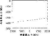
图2是表示n沟道型场效应晶体管和p沟道型场效应晶体管的漏极电流的应力依赖性的实验结果的曲线图。FIG. 2 is a graph showing experimental results of stress dependence of drain currents of n-channel field effect transistors and p-channel field effect transistors.
图2所示的结果是以下实验的结果,在Si(001)面上,对于形成的晶体管进行应力负荷实验,使得漏极电流平行于<110>轴流过。再有,评价的场效应晶体管的栅极长度是0.2μm。此外,应力的方向有相对于流过场效应晶体管的沟道的漏极电流平行方向的沟道面内单轴应力(平行于沟道的应力)、以及相对于漏极电流垂直方向的沟道面内单轴应力(垂直于沟道的应力),应力的符号正号表示拉应力,符号表示压应力。The results shown in FIG. 2 are the results of an experiment in which a stress load test was performed on the transistor formed on the Si(001) plane so that the drain current flowed parallel to the <110> axis. In addition, the gate length of the evaluated field effect transistor was 0.2 μm. In addition, the directions of stress include uniaxial stress in the channel plane (stress parallel to the channel) parallel to the direction of the drain current flowing through the channel of the field effect transistor, and channel plane in the direction perpendicular to the drain current. Internal uniaxial stress (stress perpendicular to the channel), the positive sign of the stress indicates tensile stress, and the sign indicates compressive stress.
在图2中,n沟道型场效应晶体管的情况下,漏极电流随着拉应力增加(在平行于沟道的应力中约4%/100MPa,在垂直于沟道的应力中约2%/100MPa)。In Figure 2, in the case of an n-channel field effect transistor, the drain current increases with tensile stress (about 4%/100MPa in stress parallel to the channel, about 2% in stress perpendicular to the channel /100MPa).
另一方面,在p沟道型场效应晶体管的情况下,可知漏极电流随着垂直于沟道的方向增加(约4%/100MPa),漏极电流随着平行于沟道的方向减少(约7%/100MPa)。On the other hand, in the case of a p-channel type field effect transistor, it is known that the drain current increases (about 4%/100MPa) in the direction perpendicular to the channel and decreases in the direction parallel to the channel ( about 7%/100MPa).
根据该结果,可认为在沟道面内的双轴应力情况下,在n沟道型场效应晶体管中,无论绝对值如何,漏极电流都随着拉应力增加,相反在p沟道型场效应晶体管中,在绝对值相同的双轴应力作用情况下,随着压应力增加。According to the results, it can be considered that in the case of biaxial stress in the channel plane, in the n-channel field effect transistor, the drain current increases with the tensile stress regardless of the absolute value, and on the contrary in the p-channel field effect transistor In effect transistors, in the case of biaxial stress with the same absolute value, as the compressive stress increases.
在弹性变形内的议论中应力和变形有比例关系。因此,在上述实验结果中,例如在对n沟道型场效应晶体管施加平行于沟道的拉应力时,漏极电流增加的原因被认为是构成沟道的硅的晶格与应力负荷前相比,在沟道面内平行拉伸方向上变形,使电子的迁移率增加。In discussions within elastic deformation stress and deformation are proportional. Therefore, in the above experimental results, for example, when a tensile stress parallel to the channel is applied to the n-channel type field effect transistor, the cause of the increase in the drain current is considered to be that the crystal lattice of silicon constituting the channel is different from that before the stress load. Ratio, the deformation in the parallel stretching direction in the channel plane increases the mobility of electrons.
即,本发明人发现了n沟道型场效应晶体管、p沟道型场效应晶体管的漏极电流特性依赖于构成沟道的硅晶格上产生的变形方向以及绝对值。再有,硅晶体中产生的变形可通过TEM、电子射线衍射、喇曼(Raman)分光法来测定。That is, the present inventors have found that the drain current characteristics of n-channel field effect transistors and p-channel field effect transistors depend on the direction and absolute value of strains occurring in the silicon lattice constituting the channel. In addition, the strain generated in the silicon crystal can be measured by TEM, electron beam diffraction, and Raman (Raman) spectroscopy.
可是,在晶体管这样的多层膜的叠层结构中,基于材料间的线膨胀系数的不同而产生热应力、以及基于晶格常数不同和结晶化时的膜收缩等而产生本征应力,在结构内部产生残留应力。一般地,每年微细化的发展,使场效应晶体管以其栅极长度来划代。However, in a stacked structure of multilayer films such as transistors, thermal stress occurs due to differences in linear expansion coefficients between materials, and intrinsic stress occurs due to differences in lattice constants and film shrinkage during crystallization. Residual stresses are generated inside the structure. Generally, with the development of miniaturization every year, field effect transistors are classified by their gate lengths.
本发明人进行了场效应晶体管结构的应力解析,发现了以下事实:如果推进栅极加工尺寸缩小,则因结构的微细化和新材料的采用,在结构内部产生的应力增大。特别是在栅极长度为0.1μm一代的场效应晶体管中,浅沟元件分离(STI:Shallow Trench Isolation)造成的氧化诱生应力、硅化物的反应诱生应力、多晶硅的结晶化应力等成为应力的发生源。The present inventors conducted stress analysis of the structure of field effect transistors, and found out that the stress generated inside the structure increases due to the miniaturization of the structure and the adoption of new materials as the processing size of the gate is reduced. Especially in field effect transistors with a gate length of 0.1 μm generation, oxidation-induced stress caused by STI (Shallow Trench Isolation), reaction-induced stress of silicide, crystallization stress of polysilicon, etc. become stress source of occurrence.
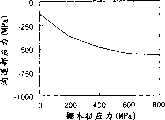
图24表示按照有限元法对各代栅极长度的场效应晶体管的沟道部分应力进行应力解析结果的曲线图。在图24中,在栅极长度比较大的2μm代的晶体管中,在栅极下的沟道部分产生的应力低,而如果为栅极长度0.25μm以下代的晶体管,则应力急剧地升高,在0.1μm代时达到2μm代的约3倍。人们正在研究场效应晶体管中产生的应力对晶体管特性的影响。例如,正在研究作为场效应晶体管特性之一的互导(Gm)的应力依赖性(Akemi Hamada、et al.、IEEE Trans.ElectronDevices、vol.38、No.4、pp.895-900、1991)。FIG. 24 is a graph showing the stress analysis results of the stress in the channel part of field effect transistors with gate lengths of various generations according to the finite element method. In FIG. 24, the stress generated in the channel portion under the gate is low in the 2 μm generation transistor with a relatively long gate length, but the stress increases sharply in the transistor of the 0.25 μm generation or less gate length. , reaching about 3 times that of the 2 μm generation at the 0.1 μm generation. The effects of stresses generated in field effect transistors on transistor characteristics are being studied. For example, the stress dependence of transconductance (Gm), which is one of the characteristics of field effect transistors, is being studied (Akemi Hamada, et al., IEEE Trans. Electron Devices, vol.38, No.4, pp.895-900, 1991) .
但是,以往场效应晶体管的特性随应力变动的情况没有问题。这是因为在0.25μm以前、即在0.25μm以上的场效应晶体管中,如图24所示,认为在晶体管结构上产生的应力小。However, conventionally, there is no problem that the characteristics of field effect transistors fluctuate with stress. This is because, as shown in FIG. 24 , in field effect transistors of 0.25 μm or more, that is, the stress generated in the transistor structure is considered to be small.
而且,还认为晶体管对自身应力的感受性也低。Furthermore, it is considered that the susceptibility of the transistor to self-stress is also low.
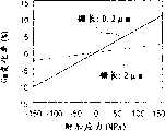
图25表示比较上述文献(Akemi Hamada、et al.、IEEE Trans.Electron Devices、vol.38、No.4、pp.895-900、1991)的互导Gm的应力依赖性的实验结果(栅极长度:2μm)和本发明人的Gm的应力依赖性的实验结果(栅极长度:0.2μm)的曲线图。Figure 25 shows the experimental results comparing the stress dependence of the transconductance Gm (gate Length: 2 μm) and the experimental results of stress dependence of Gm by the present inventors (gate length: 0.2 μm).
再有,图25中的比较,对于n沟道型场效应晶体管,在沟道的平行方向的应力负荷下进行。相对于栅极长度为2μm代的晶体管,栅极长度为0.2μm代的晶体管对于应力Gm的依赖性约增大4倍。即,随着晶体管代的发展,显示出相对于应力晶体管特性的感受性升高。In addition, the comparison in FIG. 25 was performed under the stress load in the direction parallel to the channel for the n-channel type field effect transistor. Transistors with a gate length of 0.2 μm have about a four-fold increase in dependence on stress Gm compared to transistors with a gate length of 2 μm. That is, as the transistor generation progresses, the sensitivity to stress transistor characteristics increases.
此外,根据应力解析,场效应晶体管的Si衬底的沟道部分中形成的衬底深度方向的应力分布在栅电极附近形成应力集中场。栅极长度小的0.1μm代的晶体管的扩散层的形成区域与现有的栅极长度大的晶体管相比,形成在距衬底表面近的浅区域中。其结果,在0.1μm代的晶体管中,认为元件工作区域容易受到应力的影响。Furthermore, according to stress analysis, the stress distribution in the substrate depth direction formed in the channel portion of the Si substrate of the field effect transistor forms a stress concentration field near the gate electrode. The diffusion layer formation region of the 0.1 μm generation transistor with a small gate length is formed in a shallow region closer to the substrate surface than in conventional transistors with a large gate length. As a result, in transistors of the 0.1 μm generation, it is considered that the device operating region is easily affected by stress.
因此,本发明人对于场效应晶体管结构进行基于有限元法的应力解析,对于构成场效应晶体管的材料、以及其周边材料在流过漏极电流的沟道部分的应力上产生的影响进行感度解析。Therefore, the present inventors conducted a stress analysis based on the finite element method for the field effect transistor structure, and performed a sensitivity analysis on the influence of the material constituting the field effect transistor and its surrounding materials on the stress of the channel portion through which the drain current flows. .
其结果,本发明人发现从上面包覆栅电极的膜、硅化物膜、栅电极、以及侧壁分别对沟道部分的应力产生大的影响。As a result, the present inventors found that the film covering the gate electrode from above, the silicide film, the gate electrode, and the sidewall each have a large influence on the stress of the channel portion.
根据本发明,例如通过覆盖栅电极的SiN膜本征应力的增大、或其膜厚的增加、或硅化物膜厚的增加、或栅电极本征应力的增大、或STI的氧化诱生应力的下降,可以实现使沟道部分的应力为拉应力(图3-图7)。According to the present invention, for example, through the increase of the intrinsic stress of the SiN film covering the gate electrode, or the increase of its film thickness, or the increase of the thickness of the silicide film, or the increase of the intrinsic stress of the gate electrode, or the oxidation induction of STI The reduction of the stress can make the stress of the channel part a tensile stress (FIG. 3-FIG. 7).
可是,SiN的膜应力与该膜的腐蚀速率有后述图8所示的关系,在腐蚀速率大的膜的情况下,发明人发现应力大。However, the film stress of SiN has a relationship with the corrosion rate of the film as shown in FIG. 8 described later, and the inventors found that the stress is large in the case of a film with a high corrosion rate.
鉴于上述事项,最好是构成以下的状态。In view of the above, it is preferable to configure the following states.
在被形成于衬底上、具有n沟道型场效应晶体管和p沟道型场效应晶体管的半导体器件中,沿上述n沟道型场效应晶体管的沟道部分的漏极电流流动方向的方向的残留应力,在拉应力侧大于沿上述p沟道型场效应晶体管的沟道部分的漏极电流流动方向的方向的残留应力。In a semiconductor device formed on a substrate having an n-channel type field effect transistor and a p-channel type field effect transistor, a direction along a drain current flow direction of a channel portion of the above n-channel type field effect transistor The residual stress on the tensile stress side is larger than the residual stress in the direction along the drain current flow direction of the channel portion of the p-channel type field effect transistor.
此外,在被形成于衬底上、具有n沟道型场效应晶体管和p沟道型场效应晶体管的半导体器件中,沿上述n沟道型场效应晶体管的沟道部分的漏极电流流动方向的方向的残留应力是拉应力,沿上述p沟道型场效应晶体管的沟道部分的漏极电流流动方向的方向的残留应力是压应力。Furthermore, in a semiconductor device having an n-channel type field effect transistor and a p-channel type field effect transistor formed over a substrate, the drain current flow direction along the channel portion of the above n-channel type field effect transistor The residual stress in the direction of is tensile stress, and the residual stress in the direction along the drain current flow direction of the channel portion of the p-channel type field effect transistor is compressive stress.
由此,可以同时提高n沟道型、p沟道型的漏极电流特性,所以可以实现整体性能优良的半导体器件。Thereby, the drain current characteristics of the n-channel type and the p-channel type can be simultaneously improved, so that a semiconductor device with excellent overall performance can be realized.
此外,本发明的半导体器件可以实现抑制了缺陷等的可靠性高的半导体器件。In addition, the semiconductor device of the present invention can realize a highly reliable semiconductor device in which defects and the like are suppressed.
此外,在被形成于衬底上、具有n沟道型场效应晶体管和p沟道型场效应晶体管的半导体器件中,上述各晶体管包括包覆栅电极并延伸到相邻于源-漏区域位置的绝缘膜,上述n沟道型场效应晶体管的上述绝缘膜具有比上述p沟道型场效应晶体管的上述绝缘膜大的拉应力。Furthermore, in a semiconductor device formed on a substrate having an n-channel type field effect transistor and a p-channel type field effect transistor, each of the above-mentioned transistors includes a covering gate electrode extending to a position adjacent to the source-drain region. The insulating film of the n-channel field effect transistor has a larger tensile stress than the insulating film of the p-channel field effect transistor.
上述相邻位置例如指上述绝缘膜覆盖在所述源-漏区域上部的状态。在硅化物区域形成在源-漏区域中的情况下,可以覆盖该区域来形成。The aforementioned adjacent position means, for example, a state where the aforementioned insulating film covers the upper portion of the source-drain region. In the case where the silicide region is formed in the source-drain region, it may be formed covering this region.
具体地说,为了获得上述某一方式,最好获得以下结构。Specifically, in order to obtain one of the above modes, it is preferable to obtain the following configuration.
(1)一种半导体器件,被形成于衬底上,有n沟道型场效应晶体管和p沟道型场效应晶体管,其特征在于:所述各晶体管包括将栅电极包覆,并延伸至相邻于源-漏区域位置的绝缘膜,所述绝缘膜以氮化硅为主要成分,所述n沟道型场效应晶体管的所述绝缘膜和所述p沟道型场效应晶体管的所述绝缘膜的膜厚有所不同。(1) A kind of semiconductor device, is formed on the substrate, has n-channel type field effect transistor and p-channel type field effect transistor, it is characterized in that: described each transistor includes gate electrode coating, and extends to The insulating film adjacent to the position of the source-drain region, the insulating film mainly composed of silicon nitride, the insulating film of the n-channel field effect transistor and all the p-channel field effect transistors The film thickness of the above insulating film is different.
由此,可以整体提高包括n沟道型场效应晶体管和p沟道型场效应晶体管的半导体器件的电流特性。而且,根据上述结构,即使上述绝缘膜的调整变更也不对电流特性产生影响,所以可以有效地实现上述效果。Thereby, the current characteristics of the semiconductor device including the n-channel type field effect transistor and the p-channel type field effect transistor can be improved as a whole. Furthermore, according to the above configuration, even if the adjustment and change of the above-mentioned insulating film does not affect the current characteristics, the above-mentioned effects can be effectively achieved.
再有,例如,上述绝缘膜具有比上述n沟道型场效应晶体管的上述绝缘膜大的拉应力。Furthermore, for example, the insulating film has a larger tensile stress than the insulating film of the n-channel field effect transistor.
例如,在上述n沟道型场效应晶体管和p沟道型场效应晶体管的绝缘膜残留拉应力时,使n沟道型场效应晶体管的绝缘膜比p沟道型场效应晶体管的绝缘膜厚。此外,例如,在n沟道型场效应晶体管和p沟道型场效应晶体管的绝缘膜残留压应力时,使n沟道型场效应晶体管的绝缘膜比p沟道型场效应晶体管的所述绝缘膜薄。例如最好以半导体器件中的平均膜厚为基准来比较绝缘膜厚度。For example, when tensile stress remains in the insulating films of the n-channel field effect transistor and the p-channel field effect transistor, the insulating film of the n-channel field effect transistor is thicker than the insulating film of the p-channel field effect transistor. . In addition, for example, when compressive stress remains in the insulating films of the n-channel field effect transistor and the p-channel field effect transistor, the insulating film of the n-channel field effect transistor is made larger than the p-channel field effect transistor. The insulating film is thin. For example, it is preferable to compare insulating film thicknesses based on the average film thickness in semiconductor devices.
此外,在所述半导体器件中,上述绝缘膜以氮化硅为主要成分,上述p沟道型场效应晶体管的上述绝缘膜与上述n沟道型场效应晶体管的上述绝缘膜相比,更多地含有硅(Si)、氮(N)、氧(O)、氩(Ar)、氦(He)、锗(Ge)内的至少其中之一。In addition, in the semiconductor device, the insulating film contains silicon nitride as a main component, and the insulating film of the p-channel field effect transistor is more dense than the insulating film of the n-channel field effect transistor. contains at least one of silicon (Si), nitrogen (N), oxygen (O), argon (Ar), helium (He), and germanium (Ge).
(2)此外,最好是在上述(1)中,所述绝缘膜以氮化硅为主要成分,该绝缘膜相邻于源-漏区域的延伸部分的面积在所述n沟道型场效应晶体管的所述绝缘膜和所述p沟道型场效应晶体管的所述绝缘膜之间是不同的。(2) In addition, preferably in the above (1), the insulating film mainly consists of silicon nitride, and the area of the extending portion of the insulating film adjacent to the source-drain region is larger than that of the n-channel type field. The insulating film of the effect transistor is different from the insulating film of the p-channel type field effect transistor.
也可以比较覆盖源-漏区域的长度,来取代上述面积。Instead of the aforementioned areas, the lengths covering the source-drain regions can also be compared.
具体地说,例如,在n沟道型场效应晶体管和p沟道型场效应晶体管的绝缘膜是残留拉应力的绝缘膜时,使n沟道型场效应晶体管的绝缘膜的面积大于所述p沟道型场效应晶体管的绝缘膜的面积。Specifically, for example, when the insulating films of the n-channel field effect transistor and the p-channel field effect transistor are insulating films with residual tensile stress, the area of the insulating film of the n-channel field effect transistor is made larger than the above-mentioned The area of the insulating film of the p-channel type field effect transistor.
而例如在n沟道型场效应晶体管和p沟道型场效应晶体管的绝缘膜是残留压应力的绝缘膜时,使n沟道型场效应晶体管的绝缘膜的面积小于所述p沟道型场效应晶体管的绝缘膜的面积。例如也可以以半导体器件中的平均面积为基准来比较上述面积。For example, when the insulating film of the n-channel field effect transistor and the p-channel field effect transistor is an insulating film of residual compressive stress, the area of the insulating film of the n-channel field effect transistor is smaller than that of the p-channel field effect transistor. The area of the insulating film of the field effect transistor. For example, the above-mentioned areas may be compared on the basis of the average area in the semiconductor device.
再有,也可以比较横切从绝缘膜的源极至漏极的方向的长度,来取代上述面积。具体地说,例如,在n沟道型场效应晶体管和p沟道型场效应晶体管的绝缘膜是残留拉应力的绝缘膜时,使n沟道型场效应晶体管的绝缘膜长度大于p沟道型场效应晶体管的绝缘膜的长度。In addition, instead of the above-mentioned areas, the lengths transverse to the direction from the source to the drain of the insulating film may be compared. Specifically, for example, when the insulating film of the n-channel field effect transistor and the p-channel field effect transistor is an insulating film of residual tensile stress, the length of the insulating film of the n-channel field effect transistor is longer than that of the p-channel field effect transistor. The length of the insulating film of the type field effect transistor.
而例如在n沟道型场效应晶体管和p沟道型场效应晶体管的绝缘膜是残留压应力的绝缘膜时,使n沟道型场效应晶体管的绝缘膜长度小于p沟道型场效应晶体管的绝缘膜的长度。For example, when the insulating film of the n-channel field effect transistor and the p-channel field effect transistor is an insulating film of residual compressive stress, the length of the insulating film of the n-channel field effect transistor is shorter than that of the p-channel field effect transistor. The length of the insulating film.
由此,可以整体提高包括n沟道型场效应晶体管和p沟道型场效应晶体管的半导体器件的电流特性。而且,根据该结构,即使上述绝缘膜的调整变更也不对电流特性产生影响,所以可以有效地实现上述效果。Thereby, the current characteristics of the semiconductor device including the n-channel type field effect transistor and the p-channel type field effect transistor can be improved as a whole. Furthermore, according to this configuration, even if the above-mentioned adjustment and change of the insulating film does not affect the current characteristics, the above-mentioned effect can be effectively achieved.
(3)一种半导体器件,被形成于衬底上,有n沟道型场效应晶体管和p沟道型场效应晶体管,其中,在各个所述晶体管中,在源极或漏极区域中形成硅化物区域,所述n沟道型场效应晶体管的硅化物区域的膜厚大于所述p沟道型场效应晶体管的硅化物区域的膜厚。(3) A semiconductor device formed on a substrate, having an n-channel type field effect transistor and a p-channel type field effect transistor, wherein, in each of the transistors, a source or drain region is formed In the silicide region, the film thickness of the silicide region of the n-channel field effect transistor is greater than the film thickness of the silicide region of the p-channel field effect transistor.
也可以根据半导体器件中的平均膜厚来比较所述膜厚。The film thicknesses may also be compared in terms of average film thicknesses in semiconductor devices.
由此,除了上述作为整体的提高效果以外,根据上述结构,即使上述绝缘膜的调整变更也不对电流特性产生影响,所以可以有效地实现上述效果。Therefore, in addition to the above-mentioned improvement effect as a whole, according to the above configuration, even if the adjustment and change of the above-mentioned insulating film does not affect the current characteristics, the above-mentioned effect can be effectively achieved.
(4)最好在上述(3)中,所述硅化物区域的主要成分为钴硅化物(CoSi2)、或钛硅化物(TiSi2)、或镍硅化物。(4) Preferably in the above (3), the main component of the silicide region is cobalt silicide (CoSi2 ), or titanium silicide (TiSi2 ), or nickel silicide.
(5)再有,作为另一方式,提供一种半导体器件,被形成于衬底上,有n沟道型场效应晶体管和p沟道型场效应晶体管,其中,所述n沟道型场效应晶体管的栅电极比所述p沟道型场效应晶体管的栅电极具有大的压缩膜应力。(5) Furthermore, as another way, there is provided a semiconductor device which is formed on a substrate and has an n-channel type field effect transistor and a p-channel type field effect transistor, wherein the n-channel type field effect transistor The gate electrode of the effect transistor has a larger compressive film stress than the gate electrode of the p-channel type field effect transistor.
(6)一种半导体器件,被形成于衬底上,有n沟道型场效应晶体管和p沟道型场效应晶体管,其中,所述n沟道型场效应晶体管的所述栅电极中包含的杂质在所述硅衬底的主平面的垂直方向上具有浓度梯度,所述p沟道型场效应晶体管的所述栅电极中包含的杂质在所述硅衬底的主平面的垂直方向上的测定限界内不具有浓度梯度,或者具有比n沟道型场效应晶体管的所述栅电极中的浓度梯度小的梯度。(6) A semiconductor device which is formed on a substrate and has an n-channel field effect transistor and a p-channel field effect transistor, wherein the gate electrode of the n-channel field effect transistor includes The impurity contained in the gate electrode of the p-channel type field effect transistor has a concentration gradient in the vertical direction of the main plane of the silicon substrate, and the impurity contained in the gate electrode of the p-channel field effect transistor has a concentration gradient in the vertical direction of the main plane of the silicon substrate. There is no concentration gradient within the measurement limit of the n-channel type field effect transistor, or there is a gradient smaller than the concentration gradient in the gate electrode of the n-channel field effect transistor.
例如,n沟道型场效应晶体管的栅电极的杂质浓度在硅衬底的主平面的垂直方向具有浓度梯度,p沟道型场效应晶体管的栅电极的杂质浓度分布在硅衬底的主平面的垂直方向上是均匀的。For example, the impurity concentration of the gate electrode of the n-channel field effect transistor has a concentration gradient in the vertical direction of the main plane of the silicon substrate, and the impurity concentration of the gate electrode of the p-channel field effect transistor is distributed on the main plane of the silicon substrate. is uniform in the vertical direction.
(7)一种半导体器件,被形成于衬底上,有n沟道型场效应晶体管和p沟道型场效应晶体管,其中,所述n沟道型场效应晶体管的所述栅电极的平均晶粒直径比所述p沟道型场效应晶体管的所述栅电极的平均晶粒直径小。(7) A semiconductor device which is formed on a substrate and has an n-channel field effect transistor and a p-channel field effect transistor, wherein the gate electrode of the n-channel field effect transistor has an average The grain diameter is smaller than the average grain diameter of the gate electrode of the p-channel type field effect transistor.
由此,可以整体提高包括n沟道型场效应晶体管和p沟道型场效应晶体管的半导体器件的电流特性。而且,根据该结构,通过调整位于沟道部正上方的栅电极的晶粒直径来控制应力,所以可以在沟道部有效地分配应力。Thereby, the current characteristics of the semiconductor device including the n-channel type field effect transistor and the p-channel type field effect transistor can be improved as a whole. Furthermore, according to this structure, stress is controlled by adjusting the crystal grain diameter of the gate electrode located directly above the channel portion, so that stress can be effectively distributed in the channel portion.
(8)一种半导体器件,被形成于衬底上,具有n沟道型场效应晶体管、p沟道型场效应晶体管、以及将相邻的晶体管元件进行电分离的元件分离部件,其中,所述n沟道型场效应晶体管的沟道部分和所述元件分离部件的距离比所述p沟道型场效应晶体管的沟道部分和所述元件分离部件的距离大。(8) A semiconductor device which is formed on a substrate and has an n-channel type field effect transistor, a p-channel type field effect transistor, and an element isolation member for electrically isolating adjacent transistor elements, wherein the A distance between a channel portion of the n-channel type field effect transistor and the element isolating member is greater than a distance between a channel portion of the p-channel type field effect transistor and the element isolating portion.
由此,可以整体提高包括n沟道型场效应晶体管和p沟道型场效应晶体管的半导体器件的电流特性。而且,根据该结构,如果调整掩模图形,则可以良好并且容易地实现上述效果。Thereby, the current characteristics of the semiconductor device including the n-channel type field effect transistor and the p-channel type field effect transistor can be improved as a whole. Furthermore, according to this configuration, the above effects can be achieved favorably and easily by adjusting the mask pattern.
(9)一种半导体器件,被形成于衬底上,有n沟道型场效应晶体管和p沟道型场效应晶体管,其中,向所述n沟道型场效应晶体管的沟道部照射激光时的喇曼分光的喇曼偏移比向所述p沟道型场效应晶体管的沟道部照射激光时的喇曼分光的喇曼偏移小。(9) A semiconductor device which is formed on a substrate and has an n-channel type field effect transistor and a p-channel type field effect transistor, wherein a channel portion of the n-channel type field effect transistor is irradiated with laser light The Raman shift of the Raman spectrum is smaller than the Raman shift of the Raman spectrum when the channel portion of the p-channel field effect transistor is irradiated with laser light.
例如,用TEM观察n沟道型场效应晶体管的沟道部时的晶格间隔宽于用TEM观察p沟道型场效应晶体管的沟道部时的晶格间隔。For example, when the channel portion of an n-channel field effect transistor is observed with a TEM, the lattice interval is wider than when the channel portion of a p-channel field effect transistor is observed with a TEM.
上述各试料最好使用沿横切源-漏的方向形成的试料。For each of the above-mentioned samples, it is preferable to use a sample formed in a direction transverse to the source-drain.
(10)最好在上述(1)中,所述绝缘膜以氮化硅为主要成分,所述n沟道型场效应晶体管的所述绝缘膜的腐蚀速率与所述p沟道型场效应晶体管的所述绝缘膜的腐蚀速率有所不同。(10) Preferably in the above (1), the insulating film is mainly composed of silicon nitride, and the etching rate of the insulating film of the n-channel type field effect transistor is related to that of the p-channel type field effect transistor. The etching rate of the insulating film varies among transistors.
例如,上述n沟道型场效应晶体管侧的上述绝缘膜的腐蚀速率比上述p沟道型场效应晶体管的绝缘膜的腐蚀速率小。For example, the etching rate of the insulating film on the side of the n-channel field effect transistor is lower than the etching rate of the insulating film of the p-channel field effect transistor.
(11)一种半导体器件的制造方法,该半导体器件被形成于衬底上,有n沟道型场效应晶体管和p沟道型场效应晶体管,其中,该半导体器件的制造方法包括以下步骤:在所述衬底上形成元件分离结构;在被所述元件分离结构分离的区域中形成n沟道型场效应晶体管的栅电极和p沟道型场效应晶体管的栅电极;在所述栅电极上形成覆盖栅电极的绝缘层;以及在所述n沟道型场效应晶体管的沟道部中,通过所述p沟道型场效应晶体管的沟道部,使拉应力残留在连接源极和漏极的方向上。(11) A method for manufacturing a semiconductor device, the semiconductor device is formed on a substrate, and has an n-channel field-effect transistor and a p-channel field-effect transistor, wherein the method for manufacturing the semiconductor device comprises the following steps: An element isolation structure is formed on the substrate; a gate electrode of an n-channel type field effect transistor and a gate electrode of a p-channel type field effect transistor are formed in a region separated by the element isolation structure; forming an insulating layer covering the gate electrode; and in the channel portion of the n-channel type field effect transistor, the tensile stress remains in the connection source and the channel portion of the p-channel type field effect transistor. in the direction of the drain.
作为另一方式,还提供一种半导体器件的制造方法,该半导体器件被形成于衬底上,有n沟道型场效应晶体管和p沟道型场效应晶体管,其中,该半导体器件的制造方法包括以下步骤:在所述衬底上形成元件分离结构;在被所述元件分离结构分离的区域中形成n沟道型场效应晶体管的栅电极和p沟道型场效应晶体管的栅电极;在所述栅电极上形成覆盖栅电极的绝缘层;使上述n沟道型场效应晶体管的绝缘膜比所述p沟道型场效应晶体管的绝缘膜更多地包含硅、氮、氧、氩、锗中的至少其中之一。As another way, a method for manufacturing a semiconductor device is also provided. The semiconductor device is formed on a substrate and has an n-channel field effect transistor and a p-channel field effect transistor, wherein the method for manufacturing the semiconductor device The method includes the following steps: forming an element isolation structure on the substrate; forming a gate electrode of an n-channel type field effect transistor and a gate electrode of a p-channel type field effect transistor in a region separated by the element isolation structure; An insulating layer covering the gate electrode is formed on the gate electrode; the insulating film of the n-channel type field effect transistor is made to contain more silicon, nitrogen, oxygen, argon, At least one of germanium.
另外,也可以通过腐蚀使一方的所述绝缘膜的厚度变薄/变厚。此外,也可以在形成了栅电极后,将杂质导入到n沟道型场效应晶体管的栅电极。也可以有使n沟道型场效应晶体管的电极粒径比p沟道型场效应晶体管的电极粒径小的步骤。In addition, the thickness of one of the insulating films may be reduced/thickened by etching. In addition, impurities may be introduced into the gate electrode of the n-channel field effect transistor after the gate electrode is formed. There may be a step of making the particle size of the electrode of the n-channel field effect transistor smaller than the particle size of the electrode of the p-channel field effect transistor.
例如,详细地说,在所述n沟道型场效应晶体管和所述p沟道型场效应晶体管的上部形成具有拉应力的绝缘膜时,在位于第一p沟道型场效应晶体管和相邻于所述第一p沟道型场效应晶体管的第二p沟道型场效应晶体管之间的区域中,形成比所述第一或第二p沟道型场效应晶体管上形成的所述绝缘膜薄的所述绝缘膜,或不设置所述绝缘膜进行腐蚀。For example, in detail, when an insulating film having tensile stress is formed on the upper portions of the n-channel field effect transistor and the p-channel field effect transistor, the first p-channel field effect transistor and the phase In the region between the second p-channel type field effect transistor adjacent to the first p-channel type field effect transistor, the The insulating film is thin, or the insulating film is not provided for etching.
在所述n沟道型场效应晶体管和所述p沟道型场效应晶体管的上部形成具有压应力的绝缘膜时,在位于对应于所述第一p沟道型场效应晶体管的第一n沟道型场效应晶体管和对应于所述第二p沟道型场效应晶体管的第二n沟道型场效应晶体管之间的区域中,形成比位于第一p沟道型场效应晶体管和相邻于所述第一p沟道型场效应晶体管的第二p沟道型场效应晶体管之间区域中形成的所述绝缘膜薄的所述绝缘膜,或者不设置所述绝缘膜进行腐蚀。When an insulating film having compressive stress is formed on the upper portion of the n-channel field effect transistor and the p-channel field effect transistor, at the first n channel corresponding to the first p-channel field effect transistor In the region between the channel type field effect transistor and the second n-channel type field effect transistor corresponding to the second p-channel type field effect transistor, the formation ratio is located between the first p-channel type field effect transistor and the phase The insulating film formed in the region between the second p-channel field effect transistor adjacent to the first p-channel type field effect transistor is thinner, or the insulating film is not provided to be etched.
此外,在被形成于衬底上、具有n沟道型场效应晶体管和p沟道型场效应晶体管的半导体器件中,相邻于所述n沟道型场效应晶体管的栅电极纵向方向侧面的绝缘膜的膜质量,与相邻于上述p沟道型场效应晶体管的栅电极纵向方向侧面的绝缘膜的膜质量有所不同。Furthermore, in a semiconductor device having an n-channel type field effect transistor and a p-channel type field effect transistor formed over a substrate, the side surfaces adjacent to the gate electrode longitudinal direction of the n-channel type field effect transistor The film quality of the insulating film is different from the film quality of the insulating film adjacent to the side in the longitudinal direction of the gate electrode of the p-channel type field effect transistor.
此外,在被形成于衬底上、具有n沟道型场效应晶体管和p沟道型场效应晶体管的半导体器件中,相邻于所述n沟道型场效应晶体管的栅电极纵向方向侧面的绝缘膜的膜应力在拉应力侧大于相邻于上述p沟道型场效应晶体管的栅电极纵向方向侧面的绝缘膜的膜应力。Furthermore, in a semiconductor device having an n-channel type field effect transistor and a p-channel type field effect transistor formed over a substrate, the side surfaces adjacent to the gate electrode longitudinal direction of the n-channel type field effect transistor The film stress of the insulating film is larger on the tensile stress side than the film stress of the insulating film adjacent to the side in the longitudinal direction of the gate electrode of the p-channel type field effect transistor.
最好,上述中,上述绝缘膜以氮化硅为主成份。Preferably, in the above, the insulating film is mainly composed of silicon nitride.
(12)一种半导体器件,被形成于衬底上,有n沟道型场效应晶体管和p沟道型场效应晶体管,其中,在将所述各晶体管的栅电极包覆且延伸至相邻于源-漏区域的绝缘膜的膜应力为拉应力时,相邻于栅电极纵向方向侧面的绝缘膜的扬氏模量是p沟道型场效应晶体管比n沟道型场效应晶体管小;在将所述各晶体管的栅电极包覆且延伸至相邻于源-漏区域的绝缘膜的膜应力为压应力时,相邻于栅电极纵向方向侧面的绝缘膜的扬氏模量是p沟道型场效应晶体管比n沟道型场效应晶体管大。(12) A semiconductor device is formed on a substrate and has an n-channel field effect transistor and a p-channel field effect transistor, wherein the gate electrodes of the transistors are covered and extended to adjacent When the film stress of the insulating film in the source-drain region is tensile stress, the Young's modulus of the insulating film adjacent to the side of the gate electrode in the longitudinal direction is smaller for p-channel field effect transistors than for n-channel field effect transistors; When the film stress of the insulating film covering the gate electrode of each transistor and extending to the adjacent source-drain region is compressive stress, the Young's modulus of the insulating film adjacent to the side of the gate electrode in the longitudinal direction is p A channel type field effect transistor is larger than an n-channel type field effect transistor.
由此,可整体提高包括n沟道型场效应晶体管和p沟道型场效应晶体管的半导体器件的电流特性。而且,根据上述结构,由于不对电气特性产生影响,所以可以有效地实现上述效果。Thereby, the current characteristics of the semiconductor device including the n-channel type field effect transistor and the p-channel type field effect transistor can be improved as a whole. Furthermore, according to the above configuration, since the electrical characteristics are not affected, the above effect can be effectively achieved.
(13)最好在上述(12)中,相邻于栅电极纵向方向侧面的绝缘膜的扬氏模量大的绝缘膜材质以氮化硅为主要成分,扬氏模量小的绝缘膜的材质以氧化硅为主要成分。(13) In the above (12), it is preferable that the material of the insulating film adjacent to the side of the gate electrode in the longitudinal direction has a large Young's modulus has silicon nitride as its main component, and the material of the insulating film with a small Young's modulus is The material is mainly composed of silicon oxide.
(14)一种半导体器件,被形成于衬底上,有n沟道型场效应晶体管和p沟道型场效应晶体管,其中,有多个所述n沟道型场效应晶体管和所述p沟道型场效应晶体管;在所述n沟道型场效应晶体管和所述p沟道型场效应晶体管的上部形成具有拉应力的绝缘膜;在位于第一p沟道型场效应晶体管和相邻于所述第一p沟道型场效应晶体管的第二p沟道型场效应晶体管之间的区域中,形成厚度比形成于所述第一或第二p沟道型场效应晶体管上的所述绝缘膜的厚度薄的所述绝缘膜,或不设置所述绝缘膜。(14) A semiconductor device, formed on a substrate, has an n-channel field effect transistor and a p-channel field effect transistor, wherein there are a plurality of said n-channel field effect transistors and said p Channel type field effect transistor; An insulating film with tensile stress is formed on the upper part of the n-channel type field effect transistor and the p-channel type field effect transistor; In a region between the second p-channel field effect transistor adjacent to the first p-channel type field effect transistor, a thickness ratio of that formed on the first or second p-channel type field effect transistor is formed. The insulating film is thinner, or the insulating film is not provided.
再有,所述半导体器件最好形成所述n沟道型场效应晶体管相邻配置的n沟道型场效应晶体管区域、以及所述p沟道型场效应晶体管相邻配置的p沟道型场效应晶体管区域。Furthermore, in the semiconductor device, it is preferable to form an n-channel field effect transistor region in which the n-channel field effect transistors are adjacently arranged, and a p-channel field effect transistor region in which the p-channel field effect transistors are adjacently arranged. field effect transistor region.
换句话说,在所述n沟道型场效应晶体管的栅电极和所述p沟道型场效应晶体管的栅电极上部形成具有拉应力的第一绝缘膜(例如所述应力控制膜),在位于第一p沟道型场效应晶体管和相邻于所述第一n沟道型场效应晶体管的第二p沟道型场效应晶体管之间的区域中,形成厚度比所述第一绝缘膜薄的第二绝缘膜,或不设置所述第一绝缘膜。而且,可以形成成分上不同于所述第一绝缘膜的第二绝缘膜(例如,层间绝缘膜)。In other words, a first insulating film (for example, the stress control film) having tensile stress is formed on the gate electrode of the n-channel type field effect transistor and the gate electrode of the p-channel type field effect transistor. In a region between a first p-channel type field effect transistor and a second p-channel type field effect transistor adjacent to said first n-channel type field effect transistor, an insulating film thicker than said first insulating film is formed a thin second insulating film, or the first insulating film is not provided. Also, a second insulating film (for example, an interlayer insulating film) different in composition from the first insulating film may be formed.
另外,包括:具有埋入在半导体主表面中的绝缘层的场区域;被各个上述场区域包围的第1至第4有源区域;形成在该第1、第2有源区域中的第1、第2p沟道型场效应晶体管;形成在该第3、第4有源区域中的第3、第4n沟道型场效应晶体管;以及在上述第1至第4晶体管中,包覆栅电极,延伸到相邻于源-漏区域,膜应力为拉应力的绝缘膜;上述第1、第2有源区域通过所述场区域来相邻配置,使得与主要流过所述第1、第2晶体管的漏极电流的方向一致,所述第3、第4有源区域通过所述场区域来相邻配置,所述绝缘膜包覆第1至第4晶体管,在被所述第1、第2有源区域夹置的场区域中,设置缝隙。In addition, it includes: a field region having an insulating layer buried in the main surface of the semiconductor; first to fourth active regions surrounded by each of the above-mentioned field regions; and first to fourth active regions formed in the first and second active regions. , the 2nd p-channel type field effect transistor; the 3rd, the 4th n-channel type field effect transistor formed in this 3rd, the 4th active area; And in above-mentioned 1st to 4th transistor, cover gate electrode , extending to the insulating film adjacent to the source-drain region, and the film stress is tensile stress; the above-mentioned first and second active regions are adjacently arranged through the field region, so that the main flow through the first and second active regions is The directions of the drain currents of the two transistors are the same, the third and fourth active regions are adjacently arranged through the field region, the insulating film covers the first to fourth transistors, and is covered by the first and fourth active regions. A slit is provided in the field region between the second active regions.
(15)一种半导体器件,被形成于衬底上,有n沟道型场效应晶体管和p沟道型场效应晶体管,其中,有多个所述n沟道型场效应晶体管和所述p沟道型场效应晶体管,在所述n沟道型场效应晶体管和所述p沟道型场效应晶体管的上部形成具有拉应力的绝缘膜;在位于第一p沟道型场效应晶体管和相邻于所述第一p沟道型场效应晶体管的第二p沟道型场效应晶体管之间的区域中,形成比在位于所述第一p沟道型场效应晶体管所对应的第一n沟道型场效应晶体管和所述第二p沟道型场效应晶体管所对应的所述第二n沟道型场效应晶体管之间的区域中形成的所述绝缘膜薄的所述绝缘膜,或不设置所述绝缘膜。(15) A semiconductor device, formed on a substrate, has an n-channel type field effect transistor and a p-channel type field effect transistor, wherein there are a plurality of said n-channel type field effect transistors and said p-channel type field effect transistors. channel type field effect transistor, an insulating film with tensile stress is formed on the upper part of the n-channel type field effect transistor and the p-channel type field effect transistor; In the region between the second p-channel field effect transistor adjacent to the first p-channel field effect transistor, a ratio is formed in the first n channel corresponding to the first p-channel field effect transistor. The insulating film formed in a region between the channel type field effect transistor and the second n-channel type field effect transistor corresponding to the second p-channel type field effect transistor is thin, Or the insulating film is not provided.
再有,所述绝缘膜例如相当于应力控制膜。而且,可以在所述应力控制膜上形成层间绝缘膜。In addition, the insulating film corresponds to, for example, a stress control film. Also, an interlayer insulating film may be formed on the stress control film.
此外,在被形成于衬底上、具有n沟道型场效应晶体管和p沟道型场效应晶体管的半导体器件中,有多个所述n沟道型场效应晶体管和所述p沟道型场效应晶体管,在所述n沟道型场效应晶体管和所述p沟道型场效应晶体管的上部形成具有拉应力的绝缘膜;在位于第一p沟道型场效应晶体管和相邻于所述第一p沟道型场效应晶体管的第二p沟道型场效应晶体管之间的区域中,形成厚度比在位于所述第一p沟道型场效应晶体管和对应于所述第一p沟道型场效应晶体管的所述第一n沟道型场效应晶体管之间的区域中形成的所述绝缘膜薄的所述绝缘膜,或不设置所述绝缘膜。Furthermore, in a semiconductor device having n-channel type field effect transistors and p-channel type field effect transistors formed over a substrate, there are a plurality of said n-channel type field effect transistors and said p-channel type field effect transistors A field effect transistor, forming an insulating film with tensile stress on the upper part of the n-channel field effect transistor and the p-channel field effect transistor; In the region between the first p-channel field effect transistor and the second p-channel field effect transistor, a thickness ratio is formed between the first p-channel field effect transistor and the first p-channel field effect transistor corresponding to the first p-channel field effect transistor. In the region between the first n-channel field effect transistors of channel type field effect transistors, the insulating film is formed thinner, or the insulating film is not provided.
再有,在所述任何一个方式中,在配置了所述第一p沟道型场效应晶体管的有源区域和配置了与其对应的第一n沟道型场效应晶体管的有源区域之间,也可以形成所述应力控制膜。此外,可以在所述n沟道型场效应晶体管的上部配置所述应力控制膜。Furthermore, in any one of the methods, between the active region where the first p-channel field effect transistor is arranged and the active region where the corresponding first n-channel field effect transistor is arranged , the stress control film may also be formed. In addition, the stress control film may be disposed on an upper portion of the n-channel field effect transistor.
在位于第一p沟道型场效应晶体管和第二p沟道型场效应晶体管之间的区域中,形成厚度比所述第一n沟道型场效应晶体管上部配置的所述绝缘膜(例如所述应力控制膜)薄的所述应力控制膜。In a region between the first p-channel type field effect transistor and the second p-channel type field effect transistor, the insulating film (eg, the stress control film) the stress control film is thin.
此外,在与第一p沟道型场效应晶体管的栅电极的纵向方向交叉的(例如垂直)方向的区域中,可以形成比所述第一n沟道型场效应晶体管上部形成的所述绝缘膜(例如所述应力控制膜)薄的所述绝缘膜,或者不设置所述绝缘膜。或者,在与所述第一p沟道型场效应晶体管的所述栅电极的纵向方向交叉的(例如垂直)方向的区域的相邻于形成了所述第一p沟道型场效应晶体管的有源区域的场区域中,形成比在与所述第一n沟道型场效应晶体管的栅电极的纵向方向交叉的(例如垂直)方向的区域的相邻于形成了所述第一n沟道型场效应晶体管的有源区域的场区域中形成的绝缘膜薄的所述绝缘膜,或不设置所述绝缘膜。In addition, in a region in a direction intersecting (for example, perpendicular) to the longitudinal direction of the gate electrode of the first p-channel type field effect transistor, the insulating layer formed on the upper portion of the first n-channel type field effect transistor may be formed. The insulating film may be thinner (for example, the stress control film), or the insulating film may not be provided. Alternatively, in a region in a direction intersecting (for example, perpendicular) to the longitudinal direction of the gate electrode of the first p-channel field effect transistor adjacent to the area where the first p-channel field effect transistor is formed In the field region of the active region, a region that is formed in a direction intersecting (for example, vertical) with the longitudinal direction of the gate electrode of the first n-channel type field effect transistor is adjacent to the region where the first n-channel is formed. The insulating film formed in the field region of the active region of the channel field effect transistor is thin, or the insulating film is not provided.
作为另一方式,在与第一p沟道型场效应晶体管的栅电极的纵向方向交叉的(例如垂直)方向的区域中,形成比在所述第一p沟道型场效应晶体管上部形成的所述绝缘膜(例如所述应力控制膜)薄的所述绝缘膜,或不设置所述绝缘膜。As another mode, in a region in a direction intersecting (for example, perpendicular) to the longitudinal direction of the gate electrode of the first p-channel field effect transistor, a larger than that formed on the upper portion of the first p-channel field effect transistor is formed. The insulating film (for example, the stress control film) is thin, or the insulating film is not provided.
(16)一种半导体器件,被形成于衬底上,有n沟道型场效应晶体管和p沟道型场效应晶体管,其中,有多个所述n沟道型场效应晶体管和所述p沟道型场效应晶体管;在所述n沟道型场效应晶体管和所述p沟道型场效应晶体管的上部形成具有压应力的绝缘膜;在位于所述第一p沟道型场效应晶体管所对应的第一n沟道型场效应晶体管和所述第二p沟道型场效应晶体管所对应的所述第二n沟道型场效应晶体管之间的区域中,形成比在位于第一p沟道型场效应晶体管和相邻于所述第一p沟道型场效应晶体管的第二P沟道型场效应晶体管之间的区域中形成的所述绝缘膜薄的所述绝缘膜,或不设置所述绝缘膜。(16) A semiconductor device, formed on a substrate, has an n-channel type field effect transistor and a p-channel type field effect transistor, wherein there are a plurality of said n-channel type field effect transistors and said p-channel type field effect transistors. channel type field effect transistor; an insulating film with compressive stress is formed on the upper part of the n-channel type field effect transistor and the p-channel type field effect transistor; In the area between the corresponding first n-channel field effect transistor and the second n-channel field effect transistor corresponding to the second p-channel field effect transistor, the formation ratio is in the first said insulating film being thin in said insulating film formed in a region between a p-channel type field effect transistor and a second p-channel type field effect transistor adjacent to said first p-channel type field effect transistor, Or the insulating film is not provided.
此外,可以在位于所述第一p沟道型场效应晶体管和对应于所述第一p沟道型场效应晶体管的第一n沟道型场效应晶体管之间的区域中,形成比在位于第一p沟道型场效应晶体管和相邻于所述第一p沟道型场效应晶体管的第二p沟道型场效应晶体管之间的区域中形成的所述绝缘膜薄的所述绝缘膜,或不设置所述绝缘膜。In addition, in a region between the first p-channel type field effect transistor and a first n-channel type field effect transistor corresponding to the first p-channel type field effect transistor, a ratio of The insulating film formed in a region between a first p-channel type field effect transistor and a second p-channel type field effect transistor adjacent to the first p-channel type field effect transistor is thin. film, or do not provide the insulating film.
此外,包括:具有埋入在半导体主表面中的绝缘层的场区域;被各个上述场区域包围的第1至第3有源区域;形成在该第1、第2有源区域中的第1、第2p沟道型场效应晶体管;形成在该第3有源区域中的第3n沟道型场效应晶体管;以及在上述第1至第3晶体管中,包覆栅电极,延伸到相邻于源-漏区域的位置,膜应力为压应力的绝缘膜;上述第1、第2有源区域通过所述场区域来相邻配置,使得与主要流过所述第1、第2晶体管的漏极电流的方向一致,上述绝缘膜包覆所述第1至第3晶体管,在相邻于上述第1、第2有源区域的场区域上的、与主要流过上述第1、第2晶体管的漏极电流方向的直角方向,以及相邻于上述第3有源区域的场区域周围,设置缝隙。In addition, it includes: a field region having an insulating layer buried in the main surface of the semiconductor; first to third active regions surrounded by each of the above-mentioned field regions; and a first active region formed in the first and second active regions. , the 2nd p-channel type field effect transistor; the 3rd n-channel type field effect transistor formed in the 3rd active region; and in the above-mentioned 1st to 3rd transistors, covering the gate electrode, extending to adjacent to The position of the source-drain region, the film stress is an insulating film of compressive stress; the above-mentioned first and second active regions are arranged adjacent to each other through the field region, so that the flow mainly flows through the drain of the first and second transistors The directions of the polar currents are consistent, the insulating film covers the first to third transistors, and mainly flows through the first and second transistors on the field regions adjacent to the first and second active regions. Slits are provided in the direction perpendicular to the direction of the drain current and around the field region adjacent to the third active region.
此外,在位于第一n沟道型场效应晶体管和第二n沟道型场效应晶体管之间的区域中,形成厚度比在所述第一p沟道型场效应晶体管上部配置的所述绝缘膜(例如所述应力控制膜)薄的所述应力控制膜。In addition, in a region between the first n-channel type field effect transistor and the second n-channel type field effect transistor, the insulating layer disposed on the upper portion of the first p-channel type field effect transistor is formed thicker than The stress control film is thin, such as the stress control film.
此外,在位于第一p沟道型场效应晶体管的栅电极的纵向方向的区域中,可以形成比所述第一n沟道型场效应晶体管上部形成的所述绝缘膜(例如所述应力控制膜)薄的所述绝缘膜,或不设置所述绝缘膜。或者,在与所述第一n沟道型场效应晶体管的栅电极的纵向方向交叉的(例如垂直)方向的区域的相邻于形成了所述第一n沟道型场效应晶体管的有源区域的场区域中,形成比在与所述第一p沟道型场效应晶体管的所述栅电极的纵向方向交叉的(例如垂直)方向的区域的相邻于形成了所述第一p沟道型场效应晶体管的有源区域的场区域中形成的所述绝缘膜薄的所述绝缘膜,或不设置所述绝缘膜。In addition, in a region located in the longitudinal direction of the gate electrode of the first p-channel type field effect transistor, the insulating film (such as the stress control film) formed on the upper portion of the first n-channel type field effect transistor may be formed. film) the insulating film is thin, or the insulating film is not provided. Alternatively, in a region in a direction intersecting with the longitudinal direction of the gate electrode of the first n-channel field effect transistor (for example, vertically) adjacent to the active area where the first n-channel field effect transistor is formed. In the field region of the region, the region that is formed in a direction intersecting (for example, vertical) with the longitudinal direction of the gate electrode of the first p-channel type field effect transistor is adjacent to the region where the first p-channel is formed. The insulating film formed in the field region of the active region of the channel field effect transistor is thinner, or the insulating film is not provided.
(17)在上述半导体器件中,所述绝缘膜以氮化硅为主要成分。(17) In the above semiconductor device, the insulating film contains silicon nitride as a main component.
再有,在调查公知例时,为了在沟道部中分配应力,提取了以下的关联技术,但为发现这些技术具有本发明的结构和作用效果。In addition, when investigating known examples, the following related technologies were extracted in order to distribute stress in the channel portion, but it was not found that these technologies have the structure and effect of the present invention.
例如,在(日本)特开60-52052号公报中,公开了分开制作沟道部的衬底层,即在p沟道部的下面配置尖晶石层,在n沟道部的下面配置SiO2层的方案,在特开平7-32122号公报、特开平10-92947号公报、特开平2000-243854号公报、特开平2000-160599号公报中,公开了分开制作的方案,以便将p沟道作为衬底来形成配置了Si层的SiGe层,将n沟道作为衬底来形成配置了SiGe层的Si层,在衬底区域(在流过沟道部电流的区域之下的区域(例如,距栅极绝缘膜的界面约5nm以上,在与栅极绝缘膜相反方向上分离的区域))上插入层,所以如果在其端部产生缺陷,则有在电特性上产生影响的危险。此外,在特开2000-36567号公报、特开平2000-36605号公报、特开平2001-24468号公报中,公开了对相邻于PMOS部的晶体管的元件分离部控制LOCOS的氧化量并施加压力的方案,但因LOCOS而难以有效地对应高集成化,存在分开制作造成工序大幅度增加的危险。For example, in (Japanese) Unexamined Patent Publication No. 60-52052, it is disclosed that the substrate layer of the channel portion is separately formed, that is, a spinel layer is arranged under the p-channel portion, andSiO2 is arranged under the n-channel portion. In the scheme of JP-A-7-32122, JP-A-10-92947, JP-2000-243854, JP-2000-160599, a separate fabrication scheme is disclosed, so that the p-channel Form the SiGe layer with the Si layer disposed as the substrate, and form the Si layer with the SiGe layer disposed with the n-channel as the substrate. , about 5nm or more from the interface of the gate insulating film, and a layer is inserted on the region separated in the opposite direction from the gate insulating film)), so if a defect occurs at its end, there is a danger of affecting the electrical characteristics. In addition, in JP-A-2000-36567, JP-A-2000-36605, and JP-A-2001-24468, it is disclosed that the oxidation amount of LOCOS is controlled and pressure is applied to the element isolation part of the transistor adjacent to the PMOS part. However, due to LOCOS, it is difficult to effectively respond to high integration, and there is a danger of a large increase in the number of processes caused by separate production.
附图说明Description of drawings
图1是表示本发明第1实施例的半导体器件的截面的模式图。FIG. 1 is a schematic view showing a cross section of a semiconductor device according to a first embodiment of the present invention.
图2是表示n沟道型和p沟道型场效应晶体管的漏极电流的应力依赖性的实验结果的曲线图。FIG. 2 is a graph showing experimental results of stress dependence of drain currents of n-channel and p-channel field effect transistors.
图3是表示对从上面包覆栅电极的SiN膜的本征应力在沟道部分应力上产生的影响进行解析的结果的曲线图。3 is a graph showing the results of analyzing the influence of the intrinsic stress of the SiN film covering the gate electrode on the stress of the channel portion.
图4是表示对从上面包覆栅电极的SiN膜的膜厚在沟道部分应力上产生的影响进行解析的结果的曲线图。FIG. 4 is a graph showing the results of analyzing the influence of the thickness of the SiN film covering the gate electrode on stress in the channel portion.
图5是表示对硅化物的膜厚在沟道部分应力上产生的影响进行解析的曲线图。FIG. 5 is a graph showing an analysis of the effect of the film thickness of the silicide on the stress of the channel portion.
图6是表示对栅电极的本征应力在沟道部分应力上产生的影响进行解析的曲线图。FIG. 6 is a graph showing an analysis of the influence of the intrinsic stress of the gate electrode on the stress of the channel portion.
图7是表示对STI的氧化造成的应力在沟道部分应力上产生的影响进行解析的曲线图。FIG. 7 is a graph showing an analysis of the influence of stress caused by oxidation of the STI on the stress of the channel portion.
图8是表示SiN膜应力与腐蚀速率依赖性的实验结果的曲线图。Fig. 8 is a graph showing experimental results of SiN film stress and corrosion rate dependence.
图9是表示本发明第1实施例的半导体器件截面的模式图。Fig. 9 is a schematic diagram showing a cross section of the semiconductor device according to the first embodiment of the present invention.
图10是表示本发明另一第1实施例的半导体器件截面的模式图。Fig. 10 is a schematic view showing a cross section of a semiconductor device according to another first embodiment of the present invention.
图11是表示本发明另一第1实施例的半导体器件的一部分制造工序的截面模式图。11 is a schematic cross-sectional view showing a part of the manufacturing process of the semiconductor device according to the first embodiment of the present invention.
图12是表示本发明另一第1实施例的半导体器件的一部分制造工序的截面模式图。12 is a schematic cross-sectional view showing a part of the manufacturing process of the semiconductor device according to the first embodiment of the present invention.
图13是表示本发明另一第1实施例的半导体器件的一部分制造工序的截面模式图。13 is a schematic cross-sectional view showing a part of the manufacturing process of the semiconductor device according to the first embodiment of the present invention.
图14是表示本发明第2实施例的半导体器件截面的模式图。Fig. 14 is a schematic view showing a cross section of a semiconductor device according to a second embodiment of the present invention.
图15是本发明第2实施例的半导体器件的平面模式图。Fig. 15 is a schematic plan view of a semiconductor device according to a second embodiment of the present invention.
图16是表示本发明第3实施例的半导体器件截面的模式图。Fig. 16 is a schematic view showing a cross section of a semiconductor device according to a third embodiment of the present invention.
图17是表示本发明第4实施例的半导体器件截面的模式图。Fig. 17 is a schematic view showing a cross section of a semiconductor device according to a fourth embodiment of the present invention.
图18是表示本发明第5实施例的半导体器件截面的模式图。Fig. 18 is a schematic view showing a cross section of a semiconductor device according to a fifth embodiment of the present invention.
图19是表示本发明第5实施例的半导体器件的一部分制造工序的截面模式图。19 is a schematic cross-sectional view showing a part of the manufacturing process of the semiconductor device according to the fifth embodiment of the present invention.
图20是表示本发明第5实施例的半导体器件的一部分制造工序的截面模式图。Fig. 20 is a schematic cross-sectional view showing a part of the manufacturing process of the semiconductor device according to the fifth embodiment of the present invention.
图21是表示本发明第5实施例的半导体器件的一部分制造工序的截面模式图。21 is a schematic cross-sectional view showing a part of the manufacturing process of the semiconductor device according to the fifth embodiment of the present invention.
图22是表示本发明第6实施例的半导体器件截面的模式图。Fig. 22 is a schematic view showing a cross section of a semiconductor device according to a sixth embodiment of the present invention.
图23是本发明第6实施例的半导体器件的平面模式图。Fig. 23 is a schematic plan view of a semiconductor device according to a sixth embodiment of the present invention.
图24是表示对栅极长度不同的各代沟道部分的应力进行解析的结果曲线图。FIG. 24 is a graph showing the results of analyzing the stress in the channel portion of each generation with different gate lengths.
图25是表示基于不同代的场效应晶体管的互导(Gm)与不同应力依赖性的实验结果的曲线图。FIG. 25 is a graph showing experimental results based on the dependence of mutual conductance (Gm) and stress on different generations of field effect transistors.
图26是表示本发明第7实施例的半导体器件截面的模式图。Fig. 26 is a schematic view showing a cross section of a semiconductor device according to a seventh embodiment of the present invention.
图27是表示对侧壁膜应力在沟道部分应力上产生的影响进行解析的结果的曲线图。FIG. 27 is a graph showing the results of analysis of the influence of sidewall film stress on channel portion stress.
图28是表示本发明第8实施例的半导体器件截面的模式图。Fig. 28 is a schematic view showing a cross section of a semiconductor device according to an eighth embodiment of the present invention.
图29是表示对侧壁材料在沟道部分应力上产生的影响进行解析的结果的曲线图。FIG. 29 is a graph showing the results of analyzing the influence of sidewall materials on stress in the channel portion.
图30是表示本发明第9实施例的半导体器件截面的模式图。Fig. 30 is a schematic view showing a cross section of a semiconductor device according to a ninth embodiment of the present invention.
图31是表示在本发明第1实施例的半导体器件中一例形成了接触栓塞和布线等的截面模式图。31 is a schematic cross-sectional view showing an example of formation of contact plugs, wiring lines, etc. in the semiconductor device according to the first embodiment of the present invention.
图32是本发明第10实施例的半导体器件的电路图。Fig. 32 is a circuit diagram of a semiconductor device according to a tenth embodiment of the present invention.
图33是本发明第10实施例的半导体器件的平面模式图(图34的局部放大图)。Fig. 33 is a schematic plan view of a semiconductor device according to a tenth embodiment of the present invention (partially enlarged view of Fig. 34).
图34是本发明第10实施例的半导体器件的平面模式图。Fig. 34 is a schematic plan view of a semiconductor device according to a tenth embodiment of the present invention.
图35A、图35B、图35C是表示本发明第10实施例的半导体器件截面的模式图。35A, 35B, and 35C are schematic views showing cross sections of a semiconductor device according to a tenth embodiment of the present invention.
图36是本发明第11实施例的半导体器件的平面模式图(图37的局部放大图)。Fig. 36 is a schematic plan view of a semiconductor device according to an eleventh embodiment of the present invention (partially enlarged view of Fig. 37).
图37是本发明第11实施例的半导体器件的平面模式图。Fig. 37 is a schematic plan view of a semiconductor device according to an eleventh embodiment of the present invention.
图38A、图38B、图38C是表示本发明第11实施例的半导体器件截面的模式图。38A, 38B, and 38C are schematic views showing cross sections of a semiconductor device according to an eleventh embodiment of the present invention.
图39是表示本发明第10实施例的半导体器件的一部分制造工序的截面模式图。Fig. 39 is a schematic cross-sectional view showing a part of the manufacturing process of the semiconductor device according to the tenth embodiment of the present invention.
图40是表示本发明第10实施例的半导体器件的一部分制造工序的截面模式图。Fig. 40 is a schematic cross-sectional view showing a part of the manufacturing process of the semiconductor device according to the tenth embodiment of the present invention.
图41是表示本发明第10实施例的半导体器件的一部分制造工序的截面模式图。Fig. 41 is a schematic cross-sectional view showing a part of the manufacturing process of the semiconductor device according to the tenth embodiment of the present invention.
图42是表示本发明第10实施例的半导体器件的一部分制造工序的截面模式图。Fig. 42 is a schematic cross-sectional view showing a part of the manufacturing process of the semiconductor device according to the tenth embodiment of the present invention.
图43是表示本发明第10实施例的半导体器件的一部分制造工序的截面模式图。43 is a schematic cross-sectional view showing a part of the manufacturing process of the semiconductor device according to the tenth embodiment of the present invention.
具体实施方式Detailed ways
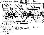
以下,用图1至图3、图8和图31来说明本发明的第1实施例。Hereinafter, a first embodiment of the present invention will be described with reference to FIGS. 1 to 3 , FIG. 8 and FIG. 31 .
图1是本发明第1实施例的半导体器件截面模式图,图2是表示n沟道及p沟道型场效应晶体管的漏极电流的应力依赖性的图,图3是表示对从上面包覆栅电极的SiN膜的本征应力在沟道部分应力(平行于漏极电流下沟道面内的应力)产生的影响进行应力解析的结果的图,图8是表示SiN膜应力与腐蚀速率依赖性的图,图31是表示一例在图1所示的半导体器件上形成了布线等的图。1 is a schematic cross-sectional view of a semiconductor device according to the first embodiment of the present invention, FIG. 2 is a graph showing the stress dependence of drain currents of n-channel and p-channel field effect transistors, and FIG. The results of stress analysis of the influence of the intrinsic stress of the SiN film covering the gate electrode on the partial stress of the channel (the stress in the channel plane parallel to the drain current) are shown. Figure 8 shows the stress and corrosion rate of the SiN film As a graph of dependence, FIG. 31 is a graph showing an example of wiring etc. formed on the semiconductor device shown in FIG. 1 .
如图1所示,本发明第1实施例的半导体器件由硅衬底1的主表面上形成的n沟道型场效应晶体管10、p沟道型场效应晶体管30、在这些晶体管10、30的上面形成的应力控制膜19、39构成。As shown in FIG. 1, the semiconductor device according to the first embodiment of the present invention consists of an n-channel type
n沟道型场效应晶体管包括在p型阱11中形成的n型源-漏(12、13)、栅极绝缘膜14、以及栅电极15,在栅电极15的上面、以及源-漏(12、13)的上面形成硅化物17、18。再有,n型源-漏是用夹置栅电极14且相互面对的12、13表示的源区或漏区。源区和漏区的不同在于电流从哪里流向哪里,没有基本结构上的不同,所以在本说明书中,表记为源-漏(12、13)。以下说明的p沟道型场效应晶体管和有关其以后的说明是相同的。The n-channel type field effect transistor includes n-type source-drain (12, 13), gate insulating film 14, and
p沟道型场效应晶体管包括在n型阱31中形成的p型源-漏(32、33)、栅极绝缘膜34、以及栅电极35,在栅电极35的上面、以及源-漏(32、33)的上面形成硅化物37、38。这些晶体管由氧化硅膜(SiO2)和氮化硅(SiN)构成,通过浅沟元件分离,与其他晶体管相互绝缘。The p-channel type field effect transistor includes p-type source-drain (32, 33), gate insulating film 34, and
栅极绝缘膜14、34例如由氧化硅膜(SiO2)、氮化硅(SiN)、氧化钛(TiO2)、氧化锆(ZrO2)、氧化铪(HfO2)、五氧化二钽(Ta2O5)等电介质膜、或它们的叠层结构构成。而栅电极15、35例如由多晶硅膜或钨(W)、铂(Pt)、钌(Ru)等金属膜或它们的叠层结构构成。The gate insulating films 14 and 34 are made of, for example, silicon oxide (SiO2 ), silicon nitride (SiN), titanium oxide (TiO2 ), zirconium oxide (ZrO2 ), hafnium oxide (HfO2 ), tantalum pentoxide ( Ta2 O5 ) and other dielectric films, or their laminated structure. The
在上述栅极绝缘膜14、34和栅电极15、35、硅化物17、18、37、38的侧壁上,形成氮化硅(SiN)、氧化硅膜(SiO2)构成的侧壁16、36。On the sidewalls of the gate insulating films 14, 34,
在n沟道型场效应晶体管、p沟道型场效应晶体管的上面,形成应力控制膜19、39,而且,在该应力控制膜19、39的上面,例如用BPSG(掺硼磷硅玻璃)膜、SOG(旋涂玻璃)膜、或TEOS(原硅酸四乙酯)膜、或按照化学汽相生长法或溅射法形成的氧化硅膜的层间绝缘膜3来覆盖。
如图31所示,将硅衬底1上形成的n沟道型场效应晶体管、p沟道型场效应晶体管通过接触栓塞和布线等进行电连接,以构成期望的电路。再有,本发明第1实施例作为控制n沟道型、p沟道型场效应晶体管的沟道部分应力的手段,是使用应力控制膜19、39的例子。对于其他部分来说,也可以是本发明第1实施例以外的结构和材料。As shown in FIG. 31 , the n-channel field effect transistors and p-channel field effect transistors formed on the
在图1的例中,省略了接触栓塞和布线等,除了图31的例子以外,对于其他实施例,同样省略了接触栓塞和布线等。In the example of FIG. 1 , contact plugs, wiring lines, etc. are omitted, and in other embodiments other than the example of FIG. 31 , contact plugs, wiring lines, etc. are similarly omitted.
应力控制膜19和应力控制膜39主要由氮化硅(SiN)构成,按照化学汽相生长法或溅射法来形成。与应力控制膜39的膜应力相比,应力控制膜19的膜应力是拉伸侧的应力。The
在LSI等半导体器件的开发中,场效应晶体管的漏极电流的提高(漏极电流的增加)被年年推进。本发明人清楚了漏极电流随应力变化的事实,在具有p沟道型场效应晶体管和n沟道型场效应晶体管的互补型场效应晶体管中,发现了有效提高n沟道型、p沟道型双方晶体管的漏极电流的方法。In the development of semiconductor devices such as LSIs, the improvement of the drain current (increase of the drain current) of field effect transistors has been promoted year by year. The present inventors have made clear the fact that the drain current varies with stress, and have found that the n-channel type, p-channel field effect transistors can effectively improve way of channeling the drain current of both transistors.
图2是表示场效应晶体管的漏极电流与应力依赖性的曲线图。由图2可知,在n沟道型场效应晶体管中,因拉应力使漏极电流增加,相反地,在p沟道型场效应晶体管中,因压应力使漏极电流增加。Fig. 2 is a graph showing the dependence of drain current on stress of a field effect transistor. It can be seen from FIG. 2 that in n-channel field effect transistors, the drain current increases due to tensile stress, and conversely, in p-channel field effect transistors, the drain current increases due to compressive stress.
另一方面,图3是表示按照有限元法对覆盖栅电极上面的SiN的膜应力在流过漏极电流的部分(沟道)的应力(在平行于漏极电流的方向上沟道面内的应力)上产生的影响进行应力解析的结果的曲线图。如图3所示,可知覆盖栅电极的膜的膜应力在拉应力侧变强时,沟道部分的应力在拉伸侧也变强。On the other hand, FIG. 3 shows the stress of the SiN film covering the gate electrode in the part (channel) through which the drain current flows according to the finite element method (in the channel plane in a direction parallel to the drain current The graph of the results of the stress analysis of the influence of the stress). As shown in FIG. 3 , it can be seen that when the film stress of the film covering the gate electrode becomes stronger on the tensile stress side, the stress of the channel portion also becomes stronger on the tensile side.
这可以被认为是包覆栅电极的膜扩展至源-漏区域的上面,这部分膜的拉应力(膜的收缩)产生使沟道部分的应力偏移到拉伸侧的现象。This can be considered as a phenomenon in which the film covering the gate electrode extends above the source-drain region, and the tensile stress (shrinkage of the film) of this part of the film shifts the stress of the channel part to the tensile side.
因此,在具有n沟道型场效应晶体管和p沟道型场效应晶体管的半导体器件中,通过覆盖n沟道型场效应晶体管的栅电极的膜使用膜应力在拉应力侧的膜,而与n沟道型的膜相比,覆盖p沟道型场效应晶体管的栅电极的膜使用膜应力在压应力侧的膜,可以期待n沟道型、p沟道型双方的漏极电流提高。因此,可以提高整体的特性。Therefore, in a semiconductor device having an n-channel type field effect transistor and a p-channel type field effect transistor, the film whose film stress is on the tensile stress side is used by the film covering the gate electrode of the n-channel type field effect transistor, while the Compared with the n-channel type film, the film covering the gate electrode of the p-channel type field effect transistor uses a film whose film stress is on the side of compressive stress, and the drain current of both n-channel type and p-channel type can be expected to be improved. Therefore, overall characteristics can be improved.
再有,本发明人还发现了氮化硅(SiN)膜的腐蚀速率与应力具有依赖性的事实。Furthermore, the present inventors have also discovered the fact that the etching rate of a silicon nitride (SiN) film depends on stress.
图8是表示一例氮化硅(SiN)膜的腐蚀速率与应力依赖性的实验结果的曲线图。从图8所示的结果可知,如果膜应力不同,则在腐蚀速率上产生差异。Fig. 8 is a graph showing an example of the experimental results of the etch rate and stress dependence of a silicon nitride (SiN) film. From the results shown in FIG. 8, it can be seen that if the film stress is different, a difference occurs in the corrosion rate.
如图1所示,本发明第1实施例的半导体器件在n沟道型场效应晶体管10的上面,形成连接到形成了硅化物18的源-漏区域12、13的应力控制膜19,包覆p沟道型场效应晶体管30的栅电极35的至少一部分,形成连接到形成了硅化物38的源-漏区域32、33的应力控制膜39,应力控制膜19的膜应力与应力控制膜39的膜应力相比为拉伸侧的应力,应力控制膜19最好是拉应力,应力控制膜39最好是压应力。As shown in FIG. 1, in the semiconductor device according to the first embodiment of the present invention, a
其结果,在沟道部分的漏极电流的平行方向的沟道面内的应力,在n沟道型时可获得强大的拉应力,相反,在p沟道型时与n沟道型相比可获得压缩侧的应力,所以可获得n沟道型、p沟道型两者的漏极电流提高的效果。As a result, the stress in the channel plane in the parallel direction of the drain current of the channel part can obtain a strong tensile stress in the n-channel type, on the contrary, when the p-channel type is compared with the n-channel type Since the stress on the compression side can be obtained, the effect of improving the drain current of both the n-channel type and the p-channel type can be obtained.
此外,应力控制膜19和应力控制膜39由氮化硅(SiN)膜构成,所以在形成层间绝缘膜3后,在源-漏区域中由上层布线实现电连接,所以可获得用作在氧化硅膜构成的层间绝缘膜3中进行接触孔开孔时的腐蚀停止层的效果。Furthermore, the
例如,接触孔形成后的接触栓塞7和布线21等变为图31所示那样。将布线层形成多层。接触栓塞7和布线21例如由钨、铝、铜、钛、氧化钛等或它们的叠层结构构成。而接触栓塞7和布线21如图31所示,例如也可以是氮化钛或钛等叠层膜构成的阻挡金属8、22的结构。For example, the contact plug 7 and the wiring 21 after the contact hole is formed are as shown in FIG. 31 . The wiring layer is formed into multiple layers. The contact plug 7 and the wiring 21 are made of, for example, tungsten, aluminum, copper, titanium, titanium oxide, etc., or a laminated structure thereof. On the other hand, as shown in FIG. 31, the contact plug 7 and the wiring 21 may have the structure of barrier metals 8 and 22 made of laminated films such as titanium nitride or titanium, for example.
应力控制膜19和应力控制膜39使用相同的成膜装置,通过改变成膜条件来获得,所以可获得即使不导入新装置也能进行的效果。The
再有,本发明第1实施例的半导体器件,n沟道型场效应晶体管的沟道部分漏极电流的平行方向的沟道面内的应力与p沟道型场效应晶体管的沟道部分的应力相比在拉应力侧,最好是上述的设n沟道型的沟道部的应力为拉应力,p沟道型沟道部的应力为压应力的方式,应力控制膜19、39中使用的膜,与应力控制膜39的膜应力相比,应力控制膜19的膜应力最好为拉伸侧的应力,如果应力控制膜19为拉应力,应力控制膜39为压应力,则不一定必须是SiN。Furthermore, in the semiconductor device of the first embodiment of the present invention, the stress in the channel plane in the direction parallel to the drain current of the channel part of the n-channel field effect transistor is the same as that of the channel part of the p-channel field effect transistor. The stress ratio is on the side of the tensile stress. It is preferable to set the stress of the n-channel type channel part as the tensile stress and the stress of the p-channel type channel part as the compressive stress as described above. The
对此,以下用图9和图4来说明构成上述状态的详细内容。On the other hand, the details of the configuration of the above state will be described below with reference to FIG. 9 and FIG. 4 .
图9是表示本发明第1实施例的半导体器件的截面结构的模式图,图4是表示场效应晶体管的沟道部分的应力与覆盖栅电极的SiN膜厚依赖性的解析结果的曲线图。9 is a schematic view showing the cross-sectional structure of the semiconductor device according to the first embodiment of the present invention, and FIG. 4 is a graph showing the analysis results of the dependence of the stress in the channel portion of the field effect transistor on the thickness of the SiN film covering the gate electrode.
该第1实施例和上述第1实施例状态通过使应力控制膜192、392的膜厚在n沟道型场效应晶体管和p沟道型场效应晶体管的部分构成的不同的膜厚,来形成上述状态,在应力控制膜为拉应力时,如图9所示,与n沟道型的应力控制膜192相比,使p沟道形的应力控制膜392薄。The first embodiment and the above-mentioned first embodiment state are formed by making the film thicknesses of the
另一方面,相反地,在应力控制膜为压应力时,与应力控制膜392相比,最好是使n沟道型一方的应力控制膜192薄(图中省略)。这些应力控制膜192、392在n沟道型、及p沟道型场效应晶体管的整个上面按照化学汽相生长法或溅射法等进行氮化硅(SiN)膜成膜后,可通过进行腐蚀等获得期望的膜厚。On the other hand, conversely, when the stress control film has a compressive stress, it is preferable to make the
再有,作为控制n沟道型、p沟道型场效应晶体管的沟道部分应力的方式,本发明的第1实施例是使用应力控制膜192、392的例子。对于其他部分来说,也可以是本发明第3实施例以外的结构或材料(其中,根据图4所示的数据来确定膜厚)。In addition, the first embodiment of the present invention is an example of using the
下面,说明本发明第3实施例的半导体器件的作用效果。Next, the operation and effect of the semiconductor device according to the third embodiment of the present invention will be described.
图4是表示沟道应力与覆盖栅电极的应力控制膜的膜厚依赖性的解析结果的图。由图4可知,应力控制膜为拉应力时,如果膜厚加厚,则沟道部分的应力向拉应力侧偏移。与此相反,在应力控制膜为压应力时,如果膜厚加厚,则意味着沟道的应力向压缩侧偏移。FIG. 4 is a graph showing analysis results of channel stress and film thickness dependence of a stress control film covering a gate electrode. It can be seen from FIG. 4 that when the stress control film is under tensile stress, if the film thickness is increased, the stress in the channel portion is shifted to the tensile stress side. On the contrary, when the stress control film is under compressive stress, increasing the film thickness means that the stress of the channel is shifted to the compressive side.
根据本发明第1实施例,在应力控制膜是拉应力时,如图9所示,p沟道型的一方薄,可提高p沟道型场效应晶体管的漏极电流。According to the first embodiment of the present invention, when the stress control film is under tensile stress, as shown in FIG. 9, the p-channel type side is thinner, and the drain current of the p-channel type field effect transistor can be increased.
另一方面,在应力控制膜为压应力时,相反地通过使n沟道型的一方薄,可获得提高n沟道型场效应晶体管的漏极电流的效果。On the other hand, when the stress control film is under compressive stress, the effect of increasing the drain current of the n-channel field effect transistor can be obtained by conversely making the n-channel type one thinner.
此外,如第1实施例所述,应力控制膜192和应力控制膜392由氮化硅(SiN)构成,所以在形成层间绝缘膜3后,在源-漏区域中由上层布线实现电连接,所以可获得用作在氧化硅膜构成的层间绝缘膜3中进行接触孔开孔时的腐蚀停止层的效果。再有,膜不限定于SiN。In addition, as described in the first embodiment, the
再有,可知绝缘膜等是残留拉应力还是残留压应力,例如,从衬底侧或从绝缘膜之上的叠层结构侧残留上述绝缘膜来变薄半导体器件,然后,残留的薄膜以衬底侧作为外侧来弯曲,则是残留拉应力的膜。另一方面,如果上述残留的薄膜以衬底侧为内侧来弯曲,则可知是残留了压应力的膜。Furthermore, it can be known whether the insulating film etc. has residual tensile stress or residual compressive stress. If the bottom side is bent as the outer side, it is a film with residual tensile stress. On the other hand, if the above-mentioned remaining thin film is bent with the substrate side as the inner side, it can be known that the compressive stress remains in the film.
本发明的第1实施例的半导体器件表示沟道部分的应力控制的一例,通过以下所述的实施例的其它方式,也可以控制沟道部分的应力。The semiconductor device of the first embodiment of the present invention represents an example of stress control in the channel portion, and the stress in the channel portion can also be controlled by other aspects of the embodiment described below.
下面,用图14、图15来说明本发明的第2实施例。图14是本发明第2实施例的半导体器件的截面(沿图15的a-a线的截面)结构的模式图,图15是从上面观察表示应力控制膜193、393的形状的模式图。再有,图15仅表示栅电极15、35、连接到源-漏的布线6、有源区域5(晶体管形成区域)、以及应力控制膜193、393的外形。而图14、图15是表示应力控制膜193、393为拉应力时的情况。Next, a second embodiment of the present invention will be described with reference to Fig. 14 and Fig. 15 . 14 is a schematic diagram showing the structure of a cross section (section along the line a-a in FIG. 15 ) of a semiconductor device according to the second embodiment of the present invention, and FIG. 15 is a schematic diagram showing the shape of the stress control films 193 and 393 viewed from above. 15 shows only the outlines of the
第2实施例与第1实施例的不同在于,在第2实施例中应力控制膜193、393的平面形状在n沟道型场效应晶体管侧和p沟道型场效应晶体管侧上有所不同。如图14所示,具有应力控制膜193、393的膜应力为拉应力时,应力控制膜392的栅电极35的侧面部分的面积比应力控制膜193的栅电极15的侧面部分面积小,而应力控制膜193、393的膜应力为压应力时,应力控制膜393的栅电极35的侧面部分面积比应力控制膜193的栅电极15的侧面部分面积大的特征。The second embodiment differs from the first embodiment in that in the second embodiment, the planar shapes of the stress control films 193, 393 are different on the side of the n-channel field effect transistor and the side of the p-channel field effect transistor. . As shown in FIG. 14 , when the film stress of the stress control films 193 and 393 is tensile stress, the area of the side portion of the
在应力控制膜193、393为拉应力时,最好是n沟道型场效应晶体管和p沟道型场效应晶体管都增大相对于栅电极15、35的延伸方向的面积(图15)。When the stress control films 193, 393 are under tensile stress, it is preferable for both the n-channel field effect transistor and the p-channel field effect transistor to increase the area with respect to the extending direction of the
相反,在应力控制膜193、393为压应力时,n沟道型场效应晶体管和p沟道型场效应晶体管都减小相对于栅电极15、35的延伸方向的面积。Conversely, when the stress control films 193 , 393 are under compressive stress, both the n-channel field effect transistor and the p-channel field effect transistor have reduced areas with respect to the extending direction of the
再有,作为控制n沟道形、p沟道型场效应晶体管的沟道部分的应力的方式,第2实施例是使用应力控制膜193、393的例子。对于其他部分来说,也可以是第2实施例以外的结构和材料。In addition, the second embodiment is an example of using the stress control films 193 and 393 as a means of controlling the stress in the channel portion of the n-channel and p-channel field effect transistors. For other parts, structures and materials other than those of the second embodiment may be used.
下面,说明本发明第2实施例的半导体器件的作用效果。Next, the operation and effect of the semiconductor device according to the second embodiment of the present invention will be described.
根据第2实施例,场效应晶体管的沟道部分的应力受应力控制膜193、393的面积控制。在延伸到源-漏区域的应力控制膜为拉应力时,在n沟道型中,尽量使面积变窄,降低沟道部分的应力。另一方面,在应力控制膜为压应力时,与此相反。According to the second embodiment, the stress of the channel portion of the field effect transistor is controlled by the area of the stress control film 193,393. When the stress control film extending to the source-drain region has tensile stress, in the n-channel type, the area is narrowed as much as possible to reduce the stress in the channel portion. On the other hand, the opposite is true when the stress control film is under compressive stress.
而且,在垂直于漏极电流的方向上,在应力控制膜是拉应力时,最好是双方的晶体管都很大地获得面积,在双方的场效应晶体管的沟道上产生拉应力,而在应力控制膜为压应力时,相反地,通过减小面积来降低沟道部分的应力。Moreover, in the direction perpendicular to the drain current, when the stress control film is under tensile stress, it is preferable that both transistors have a large area, and tensile stress is generated on the channels of both field effect transistors. When the film is under compressive stress, conversely, the stress in the channel portion is reduced by reducing the area.
因此,在本发明第2实施例的半导体器件中,如上所述,可以通过应力控制膜193、393,使沟道部分的应力与p沟道型相比在n沟道型一侧为拉应力,获得提高漏极电流的效果。Therefore, in the semiconductor device of the second embodiment of the present invention, as described above, the stress of the channel portion can be made to be tensile stress on the side of the n-channel type compared with the p-channel type by the stress control films 193 and 393. , to obtain the effect of increasing the drain current.
此外,根据本发明第2实施例,对于垂直于沟道的方向,也进行应力控制,所以可进一步获得提高漏极电流的效果。In addition, according to the second embodiment of the present invention, the stress control is also performed in the direction perpendicular to the channel, so the effect of increasing the drain current can be further obtained.
此外,根据本发明第2实施例,如上所述,应力控制膜193和应力控制膜393由氮化硅(SiN)构成,所以在形成层间绝缘膜3后,在源-漏区域中由上层布线层实现电连接,所以可获得用作在氧化硅膜构成的层间绝缘膜3中进行接触孔开孔时的腐蚀停止层的效果。Furthermore, according to the second embodiment of the present invention, as described above, the stress control film 193 and the stress control film 393 are made of silicon nitride (SiN), so after the
再有,第2实施例的半导体器件是一个一个形成n沟道型场效应晶体管和p沟道型场效应晶体管的结构,但在第2实施例中,增大表现应力控制膜的面积的部分,n沟道型或p沟道型场效应晶体管之间连续形成的部分,不一定需要使应力控制膜不连续。In addition, the semiconductor device of the second embodiment has a structure in which n-channel field effect transistors and p-channel field effect transistors are formed one by one, but in the second embodiment, the portion representing the area of the stress control film is enlarged , the portion formed continuously between n-channel type or p-channel type field effect transistors does not necessarily need to make the stress control film discontinuous.
下面,使用图10至图13来说明另一方式的例子。Next, an example of another form will be described using FIGS. 10 to 13 .
图10是其他方式的半导体器件的截面结构的模式图,图11至图13是表示另一方式的半导体器件的一部分制造工序的截面模式图。10 is a schematic cross-sectional view showing a cross-sectional structure of another semiconductor device, and FIGS. 11 to 13 are cross-sectional schematic views showing a part of manufacturing steps of another semiconductor device.
该另一方式与第1实施例的不同在于,膜的组成相互不同,以便使应力控制膜191和391表示的两个膜的应力不同。This other mode is different from the first embodiment in that the compositions of the films are different from each other so that the stresses of the two films indicated by the
在第1实施例中,希望假设不改变膜的组成时也有效果。但是,如果可接受增加用于形成其他组成的工序的风险,则最好采用该结构。In the first embodiment, it is expected that there will be an effect even if the composition of the film is not changed. However, if the risk of increasing the process steps used to form the other components is acceptable, then this structure is preferred.
具体地说,主要对于氮化硅(SiN)构成的应力控制膜191,将应力控制膜391注入形成在与应力控制膜191相同的膜中,使得氮化硅(SiN)膜过多地含有硅(Si)、氮(N)、氧(O)、锗(Ge)、氩(Ar)、氦(He)内至少其中之一。Specifically, for the
再有,作为控制n沟道型、p沟道型场效应晶体管的沟道部分应力的方式,另一方式的第1实施例是使用应力控制膜191、391的例子,对于其他部分来说,也可以是其他结构和材料。Furthermore, as a way to control the stress of the channel part of the n-channel type and p-channel type field effect transistor, the first embodiment of another mode is an example of using the
本实施例的半导体器件的应力控制膜191、391的制造工序如下。The manufacturing process of the
(1)在硅衬底1的主表面上形成n沟道型场效应晶体管10、p沟道型场效应晶体管30,形成侧壁16、36、硅化物17、18、37、38(图11)。(1) On the main surface of
(2)在n沟道型、p沟道型场效应晶体管的整个上面,例如按照溅射法或化学层生长法来进行应力控制膜191的氮化硅(SiN)膜的成膜(图12)。(2) On the entire top of the n-channel type and p-channel type field effect transistors, for example, a silicon nitride (SiN) film of the
(3)将p沟道型场效应晶体管30的上表面以外的部分作为掩模4,离子注入硅(Si)、锗(Ge)、或氮(N)、或氧(O)、或氩(Ar)等不活泼元素(图13)。(3) Using the portion other than the upper surface of the p-channel type
(4)在除去掩模4后,形成层间绝缘膜3。由此,制造图10所示结构的半导体器件。(4) After the
下面,说明本发明另一方式的第1实施例的半导体器件的作用效果。Next, the operation and effect of the semiconductor device according to the first embodiment of the present invention will be described.
根据本发明第2实施例,在将应力控制膜191成膜在整个表面(图12)上后,对覆盖p沟道型场效应晶体管的部分进行离子注入,使该部分膜的原子密度比离子注入前密。其结果,应力控制膜391的膜应力比应力控制膜191偏移到压缩侧。According to the second embodiment of the present invention, after the
因此,沟道部分漏极电流的平行方向的沟道面内应力也偏移到压缩侧,可获得提高p沟道型场效应晶体管的漏极电流的效果。Therefore, the channel in-plane stress in the direction parallel to the drain current of the channel portion is also shifted to the compressive side, and the effect of increasing the drain current of the p-channel field effect transistor can be obtained.
根据本发明另一方式的第1实施例,应力控制膜的主要成分的氮化硅(SiN)的成膜仅一次就可以。如第1实施例那样,在对不同膜应力的氮化硅进行成膜时,使用两台成膜装置,或用一台成膜装置每次改变成膜条件就可以。在难以改变成膜条件时,即使是使用多台装置,如果是本发明另一方式的第1实施例,则使用一台成膜装置,也可获得提高n沟道型、p沟道型双方的场效应晶体管的漏极电流的效果。According to the first embodiment of another aspect of the present invention, silicon nitride (SiN), which is the main component of the stress control film, can be formed only once. As in the first embodiment, when forming films of silicon nitride having different film stresses, two film forming apparatuses may be used, or one film forming apparatus may be used to change the film forming conditions each time. When it is difficult to change the film-forming conditions, even if multiple devices are used, if it is the first embodiment of another mode of the present invention, one film-forming device can be used to obtain both the n-channel type and the p-channel type. The effect of the drain current of the FET.
这样,例如,在应力控制膜191和应力控制膜391中,如果使杂质浓度不同,则在应力控制膜191和应力控制膜391中,可形成应力相互不同的结构,所以即使不导入新的装置也可对付。In this way, for example, if the impurity concentration is different in the
此外,如第1实施例说明中所述,应力控制膜191和应力控制膜391由氮化硅(SiN)构成,在形成层间绝缘膜3后,在源-漏区域中由上层布线实现电连接,所以可获得用作在氧化硅膜构成的层间绝缘膜3中进行接触孔开孔时的腐蚀停止层的效果。In addition, as described in the description of the first embodiment, the
下面,使用图16和图5说明本发明的第3实施例。Next, a third embodiment of the present invention will be described using FIG. 16 and FIG. 5 .
图16是本发明第3实施例的半导体器件的截面结构模式图,图5是表示场效应晶体管的沟道部分应力(在平行于漏极电流时沟道面内的应力)与硅化物膜厚依赖性的解析结果的曲线图。16 is a schematic diagram of a cross-sectional structure of a semiconductor device according to a third embodiment of the present invention, and FIG. 5 shows stress in the channel portion of a field effect transistor (stress in the channel plane parallel to the drain current) and silicide film thickness. A graph of the analytical results of the dependencies.
该第3实施例与第1实施例的不同在于,n沟道型场效应晶体管侧的硅化物181的膜厚比p沟道型场效应晶体管侧的硅化物381厚。这些硅化物通过(钛硅化物、钴硅化物、镍硅化物等)使用溅射法或化学汽相生长法进行钛、钴、镍等成膜后,进行热处理发生硅化反应而获得。再有,也可以没有图1所示的第1实施例的应力控制膜19、39。The third embodiment differs from the first embodiment in that the film thickness of the
再有,作为控制n沟道型、p沟道型场效应晶体管的沟道部分应力的方式,第3实施例论述了使用硅化物181、381的情况。对于其他部分来说,也可以是第3实施例以外的结构和材料。Furthermore, the third embodiment discusses the case of using
以下,说明该半导体器件的作用效果。Hereinafter, the operation and effect of this semiconductor device will be described.
n沟道型、p沟道型场效应晶体管中形成的硅化物用于以低电阻来实现接触栓塞和晶体管的电连接,还是通过热处理产生强的拉应力的材料。The silicide formed in the n-channel type and p-channel type field effect transistor is used to realize the electrical connection between the contact plug and the transistor with low resistance, and is also a material that generates strong tensile stress through heat treatment.
因此,本发明人研究利用这种硅化物的应力,将应力负载于沟道部分,来提高漏极电流。图5是表示沟道部分应力与硅化物膜厚依赖性的解析结果的曲线图。从图5可知,随着硅化物膜厚的增加,沟道部分的应力也向拉应力强的方向偏移。Therefore, the inventors of the present invention have studied to increase the drain current by applying stress to the channel portion by utilizing the stress of the silicide. FIG. 5 is a graph showing the analysis results of the dependence of stress in the channel portion on the thickness of the silicide film. It can be seen from FIG. 5 that, with the increase of the thickness of the silicide film, the stress of the channel part also shifts to the direction of strong tensile stress.
根据第3实施例,如图16所示,可获得以下效果:通过使n沟道型场效应晶体管的硅化物181的膜厚增厚,来提高n沟道型场效应晶体管的漏极电流,相反,通过使p沟道型场效应晶体管的硅化物381的膜厚变薄,来抑制p沟道型的漏极电流下降。According to the third embodiment, as shown in FIG. 16, the following effects can be obtained: the drain current of the n-channel field effect transistor is increased by increasing the film thickness of the
根据第3实施例,在形成互补型场效应晶体管上使用所需的硅化物,所以,不需要导入新材料,可获得用现有的制造工序就可以实施的效果。According to the third embodiment, since silicide is used for forming the complementary field effect transistor, it is not necessary to introduce a new material, and the effect that can be realized by the existing manufacturing process can be obtained.
下面,使用图17和图6来说明本发明的第4实施例。Next, a fourth embodiment of the present invention will be described using FIG. 17 and FIG. 6 .
图17是本发明第4实施例的半导体器件的截面结构的模式图,图6是沟道部分的应力(在平行于漏极电流下沟道面内的应力)与栅电极本征应力依赖性的解析结果。17 is a schematic diagram of the cross-sectional structure of the semiconductor device of the fourth embodiment of the present invention, and FIG. 6 shows the dependence of the stress on the channel portion (the stress in the channel plane parallel to the drain current) and the intrinsic stress of the gate electrode. analysis results.
第4实施例与第1实施例的不同在于,第4实施例中的n沟道型场效应晶体管10的栅电极151的杂质浓度分布在垂直于硅衬底1的主表面方向上有梯度,而在p沟道型场效应晶体管30的栅电极315的杂质是均匀的。The difference between the fourth embodiment and the first embodiment is that the impurity concentration distribution of the gate electrode 151 of the n-channel
第4实施例的栅电极151通过在形成栅电极后离子注入磷(P)、硼(B)、砷(As)等杂质来获得,栅电极351通过预先添加形成磷(P)、硼(B)、砷(As)等杂质来获得。再有,在第4实施例中,也可以没有图1所示的第1实施例的应力控制膜19、39。The gate electrode 151 of the fourth embodiment is obtained by ion-implanting impurities such as phosphorus (P), boron (B), arsenic (As) after forming the gate electrode, and the gate electrode 351 is formed by adding phosphorus (P) and boron (B) in advance. ), arsenic (As) and other impurities. In addition, in the fourth embodiment, the
再有,作为控制n沟道型、p沟道型场效应晶体管的沟道部分应力的方式,第4实施例论述了使用栅电极151、351的情况。对于其他部分来说,也可以是第4实施例以外的结构和材料。Furthermore, the fourth embodiment discusses the case of using the gate electrodes 151, 351 as a means of controlling stress in the channel portion of the n-channel type and p-channel type field effect transistors. For other parts, structures and materials other than those of the fourth embodiment may be used.
以下,说明第4实施例的半导体器件的作用效果。Hereinafter, operations and effects of the semiconductor device of the fourth embodiment will be described.
图6是表示沟道部分应力(平行于漏极电流下沟道面内的应力)与栅极本征应力依赖性的解析结果的曲线图。如图6所示,可知在栅电极的本征应力为拉应力时,沟道部分的应力变为压应力。FIG. 6 is a graph showing the analysis results of the dependence of channel partial stress (stress in the channel plane parallel to the drain current) and gate intrinsic stress. As shown in FIG. 6 , it can be seen that when the intrinsic stress of the gate electrode is tensile stress, the stress of the channel portion becomes compressive stress.
通常,栅电极中使用的多晶硅是形成添加了杂质的非晶硅,通过以结晶化和添加杂质的有源化为目的的热处理来获得。此时,产生基于膜收缩的拉伸的结晶化应力。另一方面,如果对没有添加杂质的非晶硅进行结晶化热处理,则应力偏移到压缩侧。Generally, the polysilicon used for the gate electrode is amorphous silicon to which impurities have been added, and is obtained by heat treatment for the purpose of crystallization and activation of the added impurities. At this time, tensile crystallization stress due to shrinkage of the film is generated. On the other hand, if crystallization heat treatment is performed on amorphous silicon to which no impurities are added, the stress is shifted to the compressive side.
根据上述两种栅电极的形成方法,前者成为膜内几乎均匀地分布杂质的多晶硅,而后者成为对于硅衬底1的主表面,在垂直方向上形成杂质分布(高斯分布或在硅衬底1的主表面垂直方向上减少浓度的分布)的多晶硅。According to the above two forming methods of the gate electrode, the former becomes polysilicon in which impurities are almost uniformly distributed in the film, while the latter becomes the main surface of the
根据第4实施例,在p沟道型场效应晶体管的栅电极中,使用杂质浓度在膜中大致均匀的拉应力的多晶硅,在n沟道型场效应晶体管的栅电极中,使用杂质浓度向衬底1侧减少的、与n沟道型使用的栅电极的应力相比具有压缩侧的应力的多晶硅。According to the fourth embodiment, for the gate electrode of the p-channel field effect transistor, tensile-stress polysilicon whose impurity concentration is substantially uniform in the film is used, and for the gate electrode of the n-channel field effect transistor, an impurity concentration close to Polysilicon that has stress on the compressive side compared to the stress of the gate electrode used in n-channel type, which is reduced on the
其结果,可获得以下效果:n沟道型场效应晶体管的沟道部分的应力与p沟道型的沟道部分相比成为拉伸侧的应力,可提高n沟道型、p沟道型双方的漏极电流。As a result, the following effects can be obtained: the stress of the channel part of the n-channel type field effect transistor becomes the stress on the tensile side compared with the channel part of the p-channel type, and the n-channel type and p-channel type can be improved. both sides of the drain current.
此外,根据第4实施例,将场效应晶体管结构中的栅电极结构用作控制沟道部分应力的手段,所以不必导入新的材料,可获得用现有的制造工序就可对付的效果。Furthermore, according to the fourth embodiment, the gate electrode structure in the field effect transistor structure is used as a means for controlling stress in the channel portion, so it is not necessary to introduce a new material, and an effect that can be dealt with by an existing manufacturing process can be obtained.
再有,第4实施例的半导体器件是在控制沟道部分应力的方式上使用栅电极应力的方式。因此,作为栅电极材料,并限定于多晶硅,例如使用钌(Ru)、铂(Pt)、钨(W)、钛(Ti)、氮化钛(TiN)等金属材料也可以,也可以是这些金属材料和多晶硅的叠层结构。例如,钌膜通过热处理成为膜应力强的拉应力。In addition, the semiconductor device of the fourth embodiment uses gate electrode stress in addition to the method of controlling stress in the channel portion. Therefore, as the gate electrode material, not limited to polysilicon, metal materials such as ruthenium (Ru), platinum (Pt), tungsten (W), titanium (Ti), and titanium nitride (TiN) may be used, and these may also be used. A stacked structure of metal material and polysilicon. For example, the ruthenium film becomes tensile stress with strong film stress by heat treatment.
因此,在p沟道型场效应晶体管的栅电极中,通过高温热处理形成拉应力大的Ru膜,在n沟道型场效应晶体管的栅电极中,形成不施加热处理的应力低的Ru膜,从而控制n沟道型、p沟道型双方的沟道部分的应力。Therefore, in the gate electrode of the p-channel field effect transistor, a Ru film with high tensile stress is formed by high-temperature heat treatment, and in the gate electrode of the n-channel field effect transistor, a Ru film with low stress without heat treatment is formed, Thereby, the stress of the channel portion of both the n-channel type and the p-channel type is controlled.
下面,使用图18至图21来说明本发明的第5实施例。Next, a fifth embodiment of the present invention will be described using FIGS. 18 to 21 .
图18是本发明第5实施例的半导体器件的截面结构的模式图,图19至图21是表示本发明第5实施例的半导体器件的一部分制造工序的截面模式图。18 is a schematic cross-sectional view of a semiconductor device according to a fifth embodiment of the present invention, and FIGS. 19 to 21 are schematic cross-sectional views showing a part of the manufacturing process of the semiconductor device according to the fifth embodiment of the present invention.
第5实施例与第4实施例的不同在于,构成n沟道型场效应晶体管10的栅电极152a、152b的晶粒在衬底1的垂直方向上有多层界面,但构成p沟道型栅电极352的晶粒不形成层,或者n沟道型的栅电极152a、152b的平均结晶粒径比p沟道型的栅电极352的平均结晶粒径小。再有,对于第5实施例来说,没有图1所示的第1实施例的应力控制膜19、39也可以。The fifth embodiment differs from the fourth embodiment in that the crystal grains constituting the
再有,作为控制n沟道型、p沟道型场效应晶体管的沟道部分应力的方式,第5实施例论述了使用栅电极152a、152b、352的情况。对于其他部分来说,也可以是第4实施例以外的结构和材料。Furthermore, the fifth embodiment discusses the case of using the
第5实施例的半导体器件的栅电极152a、152b、和352的制造工序例如如下所示。The manufacturing steps of the
(1)在硅衬底1的主表面上,形成元件分离浅沟2、n沟道型场效应晶体管10的区域的p阱11、p沟道型场效应晶体管30的区域的n阱31(图19)。(1) On the main surface of the
(2)接着,形成栅极绝缘膜14、以及栅电极152a(图20)。(2) Next, the gate insulating film 14 and the gate electrode 152 a are formed ( FIG. 20 ).
(3)接着,除去p沟道型场效应晶体管侧的栅电极152a,对栅电极152b进行成膜(图21)。(3) Next, the gate electrode 152a on the side of the p-channel field effect transistor is removed, and a film is formed on the
(4)接着,对栅电极进行加工,形成n沟道型场效应晶体管的栅电极152a、152b、p沟道型场效应晶体管的栅电极352,形成侧壁16、36、源-漏电极12、13、32、33、硅化物17、18、37、38、层间绝缘膜3(图18)。(4) Next, the gate electrode is processed to form the
以下,说明第5实施例的半导体器件的作用效果。Hereinafter, the operation and effect of the semiconductor device of the fifth embodiment will be described.
如果以非结晶形成的硅进行热处理,则随着晶粒的生长,产生拉应力。该结晶应力随着晶粒的生长而增大,所以通过减小晶粒的粒径,可以抑制结晶应力。When heat treatment is performed on amorphous silicon, tensile stress is generated along with the growth of crystal grains. Since the crystallization stress increases with the growth of the crystal grains, the crystallization stress can be suppressed by reducing the grain size of the crystal grains.
根据第5实施例,p沟道型场效应晶体管使用产生强拉应力的栅电极352,所以使沟道部分的应力成为压应力。另一方面,使n沟道型场效应晶体管的栅电极152a、152b进行两次成膜,所以栅电极152a、152b的晶粒粒径小,可缓和产生的应力,并使沟道部分的应力降低。其结果,在p沟道型场效应晶体管和n沟道型场效应晶体管双方中,可获得提高漏极电流的效果。According to the fifth embodiment, since the p-channel type field effect transistor uses the
再有,第5实施例的半导体器件的栅电极也不一定必须分两次进行成膜,也可以进行两次以上的成膜。或者,改变成膜条件等,分别用不同工序来形成n沟道型、p沟道型的栅电极,使得n沟道型晶粒小,p沟道型晶粒大。In addition, the gate electrode of the semiconductor device according to the fifth embodiment does not necessarily have to be formed twice, and may be formed more than twice. Alternatively, by changing film forming conditions, etc., different processes are used to form n-channel and p-channel gate electrodes, so that the n-channel type crystal grains are small and the p-channel type crystal grains are large.
在第5实施例中,如第4实施例中所述那样,将场效应晶体管结构中的栅电极结构用作控制沟道部分应力的手段,所以不需要导入新的材料,可获得用现有的制造工序就可对付的效果。In the fifth embodiment, as described in the fourth embodiment, the gate electrode structure in the field effect transistor structure is used as a means to control the stress of the channel part, so there is no need to introduce new materials, and the existing The manufacturing process can deal with the effect.
下面,使用图22、图23和图7来说明本发明的第6实施例。Next, a sixth embodiment of the present invention will be described using FIGS. 22 , 23 and 7 .
图22是本发明第6实施例的半导体器件的截面(沿图23的a-a’线的截面)结构的模式图,图23是从上面观察表示元件浅沟(STI)和距栅电极的距离在n沟道型场效应晶体管和p沟道型场效应晶体管上有所不同的模式图。Fig. 22 is a schematic diagram of the structure of the cross-section (the cross-section along the aa' line of Fig. 23) of the semiconductor device of the sixth embodiment of the present invention, and Fig. 23 is a view from above showing the shallow trench (STI) of the element and the distance gate electrode A pattern diagram in which distances differ between n-channel field effect transistors and p-channel field effect transistors.
再有,图23仅示出元件分离浅沟2、栅电极15、35、连接到源-漏的布线6、有源区域5(晶体管形成区域)。而图7是表示沟道部分的应力(在平行于漏极电流下沟道面内的应力)与STI氧化引起的应力依赖性的解析结果的曲线图。23 shows only the element isolation
第6实施例与第1实施例的不同在于,从n沟道型场效应晶体管10的栅电极15至元件分离浅沟2的距离(平行于沟道的方向的距离)大于从p沟道型场效应晶体管的栅电极35至元件分离浅沟2的距离(平行于沟道的方向的距离)。再有,在第6实施例中,没有图1所示的第1实施例的应力控制膜19、39也可以。The difference between the sixth embodiment and the first embodiment is that the distance from the
再有,作为控制n沟道型、p沟道型场效应晶体管的沟道部分应力的方式,第6实施例论述了使用从栅电极15至元件分离浅沟2的距离、以及从栅电极35至元件分离浅沟2的距离的情况。对于其他部分来说,也可以是第4实施例以外的结构和材料。Furthermore, as a way to control the stress of the channel part of the n-channel type and p-channel type field effect transistors, the sixth embodiment discusses the use of the distance from the
以下,说明第6实施例的半导体器件的作用效果。Hereinafter, operations and effects of the semiconductor device of the sixth embodiment will be described.
图7是表示沟道部分的应力(平行于漏极电流时沟道面内的应力)与STI氧化引起的应力依赖性的解析结果的曲线图。如图7所示,可知在降低STI引起的应力时,可降低沟道部分的大的压应力。FIG. 7 is a graph showing analysis results of the stress in the channel portion (the stress in the channel plane parallel to the drain current) and the stress dependence due to STI oxidation. As shown in FIG. 7 , it can be seen that when the stress caused by the STI is reduced, the large compressive stress in the channel portion can be reduced.
形成STI,以包围晶体管形成区域,实现晶体管之间的绝缘,但在硅衬底表面挖掘浅沟,在其中埋入氧化硅膜,所以如果在制造工序中有氧化工序,则随着氧化硅膜的形成而产生体积膨胀,在有源区域中产生大的压应力。STI is formed to surround the transistor formation area and realize insulation between transistors, but a shallow trench is dug on the surface of the silicon substrate and a silicon oxide film is buried in it, so if there is an oxidation process in the manufacturing process, the silicon oxide film will The formation of the resulting volume expansion produces a large compressive stress in the active region.
以上的结果表明沟道部分的应力极大地依赖于STI的应力。The above results indicate that the stress of the channel portion greatly depends on the stress of the STI.
根据第6实施例,n沟道型场效应晶体管的沟道部分距STI远距离形成,相反,p沟道型场效应晶体管的沟道部分在STI附近形成。由于这种STI产生的压应力如果远离STI则可以降低,所以n沟道型场效应晶体管的沟道部分的应力下降,相反,p沟道型场效应晶体管的沟道部分的应力可以形成大的压应力。According to the sixth embodiment, the channel portion of the n-channel type field effect transistor is formed at a distance from the STI, whereas the channel portion of the p-channel type field effect transistor is formed near the STI. Since the compressive stress generated by this STI can be reduced if it is far away from the STI, the stress of the channel part of the n-channel type field effect transistor is reduced, and on the contrary, the stress of the channel part of the p-channel type field effect transistor can form a large Compressive stress.
其结果,可获得提高n沟道型、p沟道型双方的漏极电流的效果。因此,可以提高整体的性能。As a result, the effect of improving the drain current of both the n-channel type and the p-channel type can be obtained. Therefore, the overall performance can be improved.
此外,根据第6实施例,仅变更布局即可,所以可获得原封不动地使用现有的制造工序的效果。Furthermore, according to the sixth embodiment, it is only necessary to change the layout, so the effect of using the existing manufacturing process as it is can be obtained.
再有,n沟道型、p沟道型双方的至栅电极15、35长边方向的STI的距离也可以都大于从STI至沟道的距离。最好是p沟道型的该距离大于n沟道型的该距离。In addition, the distance from the STI in the longitudinal direction of the
此外,第6实施例的半导体器件的特征在于,从STI至沟道的距离在n沟道型和p沟道型上有所不同,但在第6实施例以外,通过使平行于沟道方向的STI的沟宽度在n沟道型场效应晶体管侧宽,在p沟道型场效应晶体管侧窄,可获得同样的效果。In addition, the semiconductor device of the sixth embodiment is characterized in that the distance from the STI to the channel is different in the n-channel type and the p-channel type, but in addition to the sixth embodiment, by making the distance parallel to the channel direction The groove width of the STI is wider on the side of the n-channel field effect transistor and narrower on the side of the p-channel field effect transistor, and the same effect can be obtained.
再有,在这种情况下,期望两场效应晶体管的垂直于沟道方向的STI的沟宽度都宽。Also, in this case, it is desirable that both field effect transistors have wide STI channel widths perpendicular to the channel direction.
如以上那样,根据本发明的第6实施例,可以良好地增加漏极电流。此外,根据本发明第6实施例,可以实现能够降低制造成本的半导体器件。As described above, according to the sixth embodiment of the present invention, the drain current can be favorably increased. Furthermore, according to the sixth embodiment of the present invention, a semiconductor device capable of reducing manufacturing costs can be realized.
下面,用图26和图27来说明本发明的第7实施例。Next, a seventh embodiment of the present invention will be described with reference to FIGS. 26 and 27. FIG.
图26是本发明第7实施例的半导体器件的截面结构的模式图,图27是表示场效应晶体管的沟道部分的应力与侧壁膜应力依赖性的解析结果的曲线图。26 is a schematic diagram of a cross-sectional structure of a semiconductor device according to a seventh embodiment of the present invention, and FIG. 27 is a graph showing analysis results of stress dependence of channel portion of a field effect transistor and sidewall film stress.
第7实施例与第1实施例的不同在于,n沟道型场效应晶体管侧的侧壁16的膜质量与p沟道型场效应晶体管侧的侧壁36的膜质量有所不同。The seventh embodiment differs from the first embodiment in that the film quality of the
具体地说,与p沟道型场效应晶体管侧的侧壁36相比,n沟道型场效应晶体管侧的侧壁16的膜应力在拉应力侧,即侧壁16的拉应力大于侧壁36的拉应力。这些侧壁16、36的主要成分最好是氮化硅,但除此以外也可以。Specifically, compared with the
此外,期望侧壁16、36为单层膜,但也可以是氮化硅和氧化硅等的叠层结构。再有,在第1实施例中,形成了应力控制膜19、39,但在图26所示的第7实施例中,没有应力控制膜19、39也可以。In addition, the
再有,作为控制n沟道型、p沟道型场效应晶体管的沟道部分应力的方式,第7实施例论述了使用侧壁16、36的情况。对于其他部分来说,也可以是第7实施例以外的结构和材料。Furthermore, the seventh embodiment discusses the use of the
以下,说明第7实施例的半导体器件的作用效果。Hereinafter, the operation and effect of the semiconductor device of the seventh embodiment will be described.
图27所示的解析结果是假设氮化硅作为侧壁膜所获得的结果。从图27可知,侧壁的膜应力在拉应力侧,沟道部分的应力也在拉应力侧。The analytical results shown in FIG. 27 are obtained assuming silicon nitride as the sidewall film. It can be seen from FIG. 27 that the film stress of the sidewall is on the side of tensile stress, and the stress of the channel part is also on the side of tensile stress.
根据第7实施例,通过在n沟道型场效应晶体管的侧壁16中使用膜应力在拉应力侧的膜,在p沟道型场效应晶体管的侧壁36中使用膜应力与n沟道型摸相比在压应力侧的膜,可以期待提高n沟道型、p沟道型场效应晶体管双方的漏极电流。因此,可以提高整体的特性。According to the seventh embodiment, by using a film whose film stress is on the tensile stress side in the
再有,可通过膜质量(疏密)而知道膜应力的差异,膜越是致密的膜,则膜应力越在压缩侧。In addition, the difference in membrane stress can be known from the membrane quality (density), and the denser the membrane, the more the membrane stress is on the compression side.
下面,用图28和图29来说明本发明的第8实施例。Next, an eighth embodiment of the present invention will be described with reference to Fig. 28 and Fig. 29 .
图28是本发明第8实施例的场效应晶体管的截面构造的模式图,图29是表示场效应晶体管的沟道部分的应力与侧壁材料依赖性的解析结果的曲线图。28 is a schematic diagram of a cross-sectional structure of a field effect transistor according to an eighth embodiment of the present invention, and FIG. 29 is a graph showing analysis results of stress in a channel portion of a field effect transistor and sidewall material dependence.
第8实施例与第1实施例的不同在于,应力控制膜9如第1实施例那样在n沟道型场效应晶体管侧和p沟道型场效应晶体管侧没有膜应力的差异。The eighth embodiment differs from the first embodiment in that the
而且,在第8实施例中,在应力控制膜9的膜应力为拉应力时,侧壁16的平均扬氏模量比侧壁36的平均扬氏模量大,例如,侧壁16主要由氮化硅构成,而侧壁36主要由氧化硅构成。Moreover, in the eighth embodiment, when the film stress of the
另一方面,应力控制膜9的膜应力为压应力时,侧壁16的平均扬氏模量比侧壁36的平均扬氏模量小,例如,侧壁16主要由氧化硅构成,而侧壁36主要由氮化硅构成。On the other hand, when the film stress of the
再有,侧壁16、36也可以是多种材料构成的叠层结构。此外,第8实施例根据侧壁的扬氏模量(硬度),利用不将从上面覆盖栅电极和侧壁的膜的应力传递到沟道部分的现象。Furthermore, the
因此,覆盖栅电极和侧壁的膜很重要,即使没有应力控制膜也可以。但是,还存在层间绝缘膜3的应力作用于侧壁16、36的情况,所以在没有应力控制膜的情况下,在层间绝缘膜3的应力为拉应力时,使侧壁16的扬氏模量大于侧壁36的扬氏模量,而在层间绝缘膜3的应力为压应力时,使侧壁16的扬氏模量小于侧壁36的扬氏模量。Therefore, the film covering the gate electrode and side walls is important even without the stress control film. However, there are cases where the stress of the
再有,作为控制n沟道型、p沟道型场效应晶体管的沟道部分应力的方式,第8实施例论述了使用侧壁16、36,而且使用从上面覆盖栅电极和侧壁的膜的情况。对于其他部分来说,也可以是第7实施例以外的结构和材料。Furthermore, the eighth embodiment discusses the use of the
下面,说明第8实施例的半导体器件的作用效果。Next, the operation and effect of the semiconductor device of the eighth embodiment will be described.
图29是表示沟道部的应力与侧壁材料依赖性的解析结果的曲线图。其中,图29所示的结果是假设在扬氏模量低的材料中氧化硅作为侧壁材料,在扬氏模量高的材料中氮化硅作为侧壁材料来进行计算所获得的结果。FIG. 29 is a graph showing the analysis results of the dependence of the stress of the channel portion on the sidewall material. The results shown in FIG. 29 are calculated assuming that silicon oxide is used as the sidewall material among materials with low Young's modulus, and silicon nitride is used as the sidewall material among materials with high Young's modulus.
如图29所示,比较侧壁材料为氧化硅的情况和氮化硅的情况时,应力控制膜9为拉应力时,氮化硅的情况在拉应力侧大,而在应力控制膜9为压应力时,氧化硅的情况在拉应力侧大。As shown in FIG. 29, when comparing the case where the side wall material is silicon oxide and the case of silicon nitride, when the
根据第8实施例,在应力控制膜9为拉应力时,在n沟道型场效应晶体管的侧壁16中使用氮化硅,在p沟道型场效应晶体管的侧壁36中使用氧化硅。According to the eighth embodiment, when the
与上述相反,在应力控制膜9为压应力时,在n沟道型场效应晶体管的侧壁16中使用氧化硅,在p沟道型场效应晶体管的侧壁36中使用氮化硅。Contrary to the above, when the
因此,可以期待提高n沟道型、p沟道型场效应晶体管双方的漏极电流。因此,可以提高整体特性。Therefore, it can be expected that the drain currents of both n-channel type and p-channel type field effect transistors can be improved. Therefore, overall characteristics can be improved.
再有,膜的扬氏模量也可通过微小压入试验等来测定。In addition, the Young's modulus of a film can also be measured by micro-indentation test etc.
下面,用图30来说明本发明的第9实施例。Next, a ninth embodiment of the present invention will be described with reference to FIG. 30 .
图30是本发明第9实施例的半导体器件的截面结构的模式图。Fig. 30 is a schematic diagram of a cross-sectional structure of a semiconductor device according to a ninth embodiment of the present invention.
第9实施例的特征在于,在应力控制膜19的膜应力为拉应力,应力控制膜39的膜应力为压应力时,进行侧壁16的膜应力为拉应力、侧壁36的膜应力为压应力的组合。The ninth embodiment is characterized in that when the film stress of the
再有,应力控制膜19、39最好主要是氮化硅膜,但也可以除此以外来构成。Note that the
侧壁16、36最好主要是氮化硅构成的膜,但也可以是与氧化硅等的叠层结构,或是除此以外的材料。The
而且,作为控制n沟道型、p沟道型场效应晶体管的沟道部分应力的方式,第9实施例是使用应力控制膜19、39和侧壁16、36的例子。因此,对于其他部分来说,也可以是第9实施例以外的结构和材料。Furthermore, the ninth embodiment is an example of using
下面,说明第9实施例的半导体器件的作用效果。Next, the effects of the semiconductor device of the ninth embodiment will be described.
根据本发明第9实施例,如第1实施例说明的那样,应力控制膜19是拉应力,应力控制膜39是压应力,所以可以提高n沟道型、p沟道型场效应晶体管双方的漏极电流。According to the ninth embodiment of the present invention, as described in the first embodiment, the
而且,根据第9实施例,如第8实施例说明的那样,通过以扬氏模量大材料、例如氮化硅来形成侧壁,可以进一步提高n沟道型、p沟道型场效应晶体管双方的漏极电流。Moreover, according to the ninth embodiment, as described in the eighth embodiment, by forming the sidewalls with a material having a large Young's modulus, such as silicon nitride, the performance of n-channel and p-channel field effect transistors can be further improved. both sides of the drain current.
此外,根据第9实施例,如第7实施例说明的那样,通过使侧壁16为拉应力,侧壁36为压应力,可以进一步提高n沟道型、p沟道型场效应晶体管双方的漏极电流。In addition, according to the ninth embodiment, as described in the seventh embodiment, by making the sidewall 16 a tensile stress and the sidewall 36 a compressive stress, the performance of both the n-channel and p-channel field effect transistors can be further improved. drain current.
此外,应力控制膜19和侧壁16可以按相同的成膜条件进行成膜,而且,应力控制膜39和侧壁36可以按相同的成膜条件进行成膜,所以可获得简化制造工序的效果。In addition, the
再有,对于上述例子来说,除了图31的例子以外,省略示出接触栓塞,但通过改变形成于n沟道型场效应晶体管侧的接触栓塞的形状、以及形成于p沟道型场效应晶体管侧的接触栓塞的形状,可以改变n沟道形和p沟道型中作用的应力。Furthermore, for the above example, except for the example in FIG. 31 , the contact plug is omitted, but by changing the shape of the contact plug formed on the side of the n-channel field effect transistor and the The shape of the contact plug on the transistor side can change the stress acting on the n-channel type and the p-channel type.
下面,用图2、图32至图35来说明本发明的第10实施例。本实施例是实际的器件电路应用例,在第2实施例中,在应力控制膜9具有拉应力的膜应力情况下,还考虑了垂直于沟道方向。图2是表示n沟道型和p沟道型场效应晶体管的漏极电流与应力依赖性的实验结果的图,图32是表示采用了本发明的双NAND电路的电路图,图33、图34是表示本发明的半导体器件的平面布局的模式图(图33是放大图34的一部分(X所示的框内附近)的模式图),图35是表示从图33的平面布局A到D的截面结构的模式图。Next, a tenth embodiment of the present invention will be described with reference to FIGS. 2, 32 to 35. FIG. This embodiment is an actual device circuit application example. In the second embodiment, when the
如图32所示,采用了本发明的电路是由两个p沟道型场效应晶体管P1、P2、两个n沟道型场效应晶体管N1、N2构成的双NAND电路。这些晶体管N1、N2、P1、P2分别对应于图33所示的晶体管N1、N2、P1、P2。As shown in FIG. 32 , the circuit using the present invention is a dual NAND circuit composed of two p-channel field effect transistors P1 and P2 and two n-channel field effect transistors N1 and N2. These transistors N1, N2, P1, and P2 correspond to the transistors N1, N2, P1, and P2 shown in FIG. 33, respectively.
在图33中,一个双NAND电路由共有栅电极FG的p沟道型场效应晶体管P1和n沟道型场效应晶体管N2、与其同样的P2和N1、用于实现各个晶体管的电连接的接触栓塞CONT、以及布线ML构成。这里,将所述p沟道型场效应晶体管P1、P2形成在一个有源区ACT1上,将n沟道型场效应晶体管N1、N2形成在一个有源区ACT2上。In FIG. 33, a dual NAND circuit consists of a p-channel field effect transistor P1 and an n-channel field effect transistor N2 that share a gate electrode FG, the same P2 and N1, and a contact for realizing the electrical connection of each transistor. The plug CONT and the wiring ML are constituted. Here, the p-channel field effect transistors P1 and P2 are formed on one active region ACT1, and the n-channel field effect transistors N1 and N2 are formed on one active region ACT2.
本实施例的半导体器件是连续并且重复多个双NAND电路的图形。即,如图34所示,重复排列多个p沟道型场效应晶体管P1、P2和n沟道型场效应晶体管N1、N2,由n沟道型场效应晶体管连续的区域NM和p沟道型场效应晶体管连续的区域PM构成。The semiconductor device of this embodiment is a continuous and repeated pattern of a plurality of dual NAND circuits. That is, as shown in FIG. 34, a plurality of p-channel type field effect transistors P1, P2 and n-channel type field effect transistors N1, N2 are repeatedly arranged, and the region NM and the p-channel type field effect transistor are continuous by the n-channel type field effect transistor. Type field effect transistor continuous area PM constitutes.
这里,在本实施例中,第2实施例所述的应力控制膜有拉应力的膜应力,n沟道型、p沟道型场效应晶体管的形成部分分别以图33、图34所示的平面图形来形成。即,在覆盖整个电路布局的应力控制膜中,流过p沟道型场效应晶体管的漏极电流的方向的应力控制膜具有在被有源的p沟道型场效应晶体管夹置的场上不连续的特征(应力控制膜209在图33所示的晶体管电路中,在被有源的p沟道型场效应晶体管夹置的场以外的部分,在晶体管的栅电极纵向方向、n沟道型场效应晶体管的连续方向上,应力控制膜连续形成至另一元件上)。Here, in this embodiment, the stress control film described in the second embodiment has a film stress of tensile stress, and the forming parts of n-channel type and p-channel type field effect transistors are shown in Fig. 33 and Fig. 34 respectively. to form flat graphics. That is, in the stress control film covering the entire circuit layout, the stress control film in the direction of the drain current flowing through the p-channel type field effect transistor has on the field sandwiched by the active p-channel type field effect transistor. Discontinuous features (the
宏观地观察它时,如图34所示,在形成多个p沟道型场效应晶体管的区域PM中,在应力控制膜209中形成缝隙(膜不连续的部分)。When viewed macroscopically, as shown in FIG. 34 , gaps (film discontinuity portions) are formed in the
图33的平面布局图中的截面结构A~D的模式图示于图35。与第2实施例同样,本实施例的半导体器件被形成在硅衬底201的主表面上,由n沟道型场效应晶体管210、p沟道型场效应晶体管230、形成在这些晶体管上面的应力控制膜209构成。A schematic view of cross-sectional structures A to D in the planar layout view of FIG. 33 is shown in FIG. 35 . Like the second embodiment, the semiconductor device of this embodiment is formed on the main surface of a
n沟道型场效应晶体管由形成在p型阱211中的n型源-漏(212、213)、栅极绝缘膜214、栅电极215构成,在栅电极215的上面和源-漏(212、213)的上面,形成硅化物217、218。而p沟道型场效应晶体管由形成在n型阱231中的p型源-漏(232、233)、栅极绝缘膜34、栅电极35构成,在栅电极235的上面和源-漏(232、233)的上面,形成硅化物237、238。此外,在栅极绝缘膜214、234和栅电极215、235、硅化物217、218、237、238的侧壁上形成侧壁216、236。这些晶体管通过元件分离浅沟202形成与其他晶体管的绝缘。The n-channel type field effect transistor is made up of n-type source-drain (212, 213),
在n沟道型、p沟道型场效应晶体管的上面,形成应力控制膜209,而且在其上面,形成通过接触栓塞207进行电连接的布线223和层间绝缘膜203。A
应力控制膜209的其膜应力为拉应力,使用第1实施例中论述的材料和成膜方法,在横切p沟道型场效应晶体管的源-漏的截面(图34的A-B截面、图35A)中,元件分离浅沟中不连续地形成,元件分离浅沟例如在夹置202a下,无论相邻的晶体管如何,应力控制膜不是连续的。另一方面,在横切n沟道型场效应晶体管的截面(图34的C-D截面,图35C)中,无论相邻的晶体管如何,应力控制膜是连续的。即,在元件分离浅沟上,例如在202d、202e上应力控制膜是连续的。The film stress of the
此外,如图34的B-C截面和图35B所示,在n沟道型、p沟道型场效应晶体管的栅电极纵向方向的元件分离浅沟上,例如在202c上也形成应力控制膜209,使栅电极纵向方向的晶体管上或其他元件上的应力控制膜连续。In addition, as shown in the B-C section of FIG. 34 and FIG. 35B, the
再有,本实施例所示的双NAND电路是将本发明应用于实际的电路布局的一个例子。平面布局也可以是本实施例以外的布局,采用的电路例如也可以是AND电路、NOR电路、OR电路、输入输出缓冲电路。此外,就应力控制膜以外的结构和材料、制造方法来说,也可以是本实施例以外的结构、材料、及制造方法。In addition, the dual NAND circuit shown in this embodiment is an example of applying the present invention to an actual circuit layout. The plane layout may also be a layout other than this embodiment, and the circuits used may also be, for example, AND circuits, NOR circuits, OR circuits, and input-output buffer circuits. In addition, structures, materials, and manufacturing methods other than the stress control film may be structures, materials, and manufacturing methods other than those of this embodiment.
以下,说明本实施例的作用效果。如第2实施例所述那样,场效应晶体管的沟道部分的应力可以根据应力控制膜9的区域的宽度来控制。第2实施例的图14是在n沟道型、p沟道型场效应晶体管中主要将平行于沟道方向的应力最佳化的图。Hereinafter, the operation and effect of this embodiment will be described. As described in the second embodiment, the stress of the channel portion of the field effect transistor can be controlled by the width of the region of the
可是,如图2所示,n沟道型、p沟道型场效应晶体管的漏极电流不仅因平行于沟道方向应力而极大变化,而且因垂直于沟道方向的应力而极大变化,垂直于沟道方向的拉应力为100MPa时,n沟道型场效应晶体管的应力约增加2%,p沟道型场效应晶体管的应力约减少7%。However, as shown in Figure 2, the drain current of n-channel and p-channel field effect transistors varies greatly not only due to stress parallel to the direction of the channel, but also greatly changes due to stress perpendicular to the direction of the channel , when the tensile stress perpendicular to the channel direction is 100MPa, the stress of the n-channel field effect transistor increases by about 2%, and the stress of the p-channel field effect transistor decreases by about 7%.
在实际器件的电路中,由于使膜平面地形成,所以在晶体管的沟道部分中,两轴应力、即平行方向和垂直方向的应力产生作用。在将膜应力为拉应力的应力控制膜整个电路面上一样地进行成膜时,在晶体管的沟道部分中平行方向、垂直方向上同时产生拉应力。In the circuit of an actual device, since the film is formed planarly, biaxial stress, that is, stress in parallel and perpendicular directions, acts on the channel portion of the transistor. When the stress control film whose film stress is tensile stress is uniformly formed on the entire circuit surface, tensile stress is simultaneously generated in the parallel direction and the vertical direction in the channel portion of the transistor.
对于n沟道型场效应晶体管来说,平行、垂直于沟道方向的拉应力使漏极电流增加,所以可以期待提高特性。For n-channel field effect transistors, the tensile stress in the direction parallel to or perpendicular to the channel increases the drain current, so it can be expected to improve the characteristics.
可是,p沟道型场效应晶体管因平行于沟道方向的拉应力使漏极电流减少,所以需要降低该拉应力。但是,对于垂直于沟道的方向来说,可以使漏极电流增加,所以想有效地灵活使用它。However, in p-channel type field effect transistors, the drain current decreases due to the tensile stress parallel to the channel direction, so it is necessary to reduce the tensile stress. However, for the direction perpendicular to the channel, the drain current can be increased, so I want to use it effectively.
因此,根据本实施例的半导体器件,在覆盖了整个电路的应力控制膜中,对于平行于p沟道型场效应晶体管的沟道方向,通过除去应力控制膜,可以降低平行于p沟道型场效应晶体管的沟道方向的拉应力。对于除此以外的方向,即平行于n沟道型场效应晶体管的沟道方向、垂直于n沟道型、p沟道型场效应晶体管的沟道方向,可以使拉应力起作用。Therefore, according to the semiconductor device of this embodiment, in the stress control film covering the entire circuit, with respect to the channel direction parallel to the p-channel type field effect transistor, by removing the stress control film, it is possible to reduce the channel direction parallel to the p-channel type field effect transistor. Tensile stress in the channel direction of a field effect transistor. In other directions, that is, parallel to the channel direction of n-channel field effect transistors and perpendicular to the channel directions of n-channel and p-channel field effect transistors, tensile stress can act.
因此,n沟道型、p沟道型场效应晶体管同时进行沟道面内的双轴方向的应力控制,所以可以获得同时增加n沟道型、p沟道型的漏极电流的效果。Therefore, the n-channel type and the p-channel type field effect transistor simultaneously perform biaxial stress control in the channel plane, so that the effect of simultaneously increasing the drain current of the n-channel type and the p-channel type can be obtained.
作为应力控制膜的材料,将第1实施例中氮化硅列举为一个例子。由此,应力控制膜主要可以用作在氧化硅构成的层间绝缘膜中打开接触孔的自匹配接触膜。As a material of the stress control film, silicon nitride in the first embodiment is cited as an example. Thus, the stress control film can be mainly used as a self-matching contact film that opens a contact hole in an interlayer insulating film made of silicon oxide.
本实施例的半导体器件仅在被有源p沟道型场效应晶体管夹置的场区域上除去应力控制膜。即,对于在p沟道型场效应晶体管的源-漏上连接接触栓塞的部分,形成应力控制膜,所以可获得将其用作自匹配接触膜的效果。The semiconductor device of this embodiment removes the stress control film only on the field region sandwiched by the active p-channel type field effect transistors. That is, since the stress control film is formed on the portion where the contact plug is connected to the source-drain of the p-channel type field effect transistor, the effect of using it as a self-matching contact film can be obtained.
此外,本实施例所述的应力控制膜加工可以在与形成自匹配接触孔相同的工序中进行,所以掩模可以与自匹配接触共有。即,在对应力控制膜209一样地进行成膜后,在与自匹配接触孔形成处理的同时,可以进行应力控制膜加工处理(除去元件分离浅沟202c和202b上的应力控制膜)。其后的加工可连续进行以往的自匹配接触的处理。这样,根据本实施例,仅变更掩模布局,就可以使用以往的处理,所以可获得制造成本良好的半导体器件的效果。In addition, the processing of the stress control film described in this embodiment can be performed in the same process as that of forming the self-matching contact hole, so the mask can be shared with the self-matching contact. That is, after the
再有,尽量减小在平行于p沟道型场效应晶体管的沟道方向上产生的拉应力。因此,期望p沟道型场效应晶体管侧的应力控制膜仅形成在用作自匹配接触的部分上。Furthermore, the tensile stress generated in the direction parallel to the channel of the p-channel field effect transistor is minimized. Therefore, it is desirable that the stress control film on the side of the p-channel type field effect transistor is formed only on a portion serving as a self-matching contact.
再有,应力控制膜的缝隙部分不一定需要是完全没有膜的状态。也可以形成少许薄的膜。In addition, the gap portion of the stress control film does not necessarily need to be in a state where there is no film at all. A slightly thin film may also be formed.
作为另一方式,在位于第一p沟道型场效应晶体管和相邻于所述第一p沟道型场效应晶体管的第二p沟道型场效应晶体管之间的区域(例如场区域)、以及位于所述第一p沟道型场效应晶体管和对应于所述第一p沟道型场效应晶体管的第一n沟道型场效应晶体管之间的区域(例如场区域)中,可以形成厚度比形成于所述第一p沟道型场效应半导体上的所述应力控制膜薄的所述应力控制膜,或不设置所述应力控制膜。As another way, in the region between the first p-channel field effect transistor and the second p-channel field effect transistor adjacent to the first p-channel field effect transistor (for example, field region) , and in a region (such as a field region) between the first p-channel field effect transistor and a first n-channel field effect transistor corresponding to the first p-channel field effect transistor, may The stress control film is formed thinner than the stress control film formed on the first p-channel type field effect semiconductor, or the stress control film is not provided.
或者,在位于第一p沟道型场效应晶体管和相邻于所述第一p沟道型场效应晶体管的第二p沟道型场效应晶体管之间的区域(例如场区域)、以及位于对应于所述第一p沟道型场效应晶体管的第一n沟道型场效应晶体管和相邻于所述第一n沟道型场效应晶体管并对应于所述第二p沟道型场效应晶体管的第二n沟道型场效应晶体管之间的区域(例如场区域)中,可以形成厚度比形成于所述第一n沟道型场效应晶体管上的所述应力缓和层薄的所述应力缓和层,或也可考虑不设置所述应力缓和层。Alternatively, in a region (such as a field region) between the first p-channel field effect transistor and a second p-channel field effect transistor adjacent to the first p-channel field effect transistor, and A first n-channel field effect transistor corresponding to the first p-channel field effect transistor and a field effect transistor adjacent to the first n-channel field effect transistor and corresponding to the second p-channel field effect transistor In a region between the second n-channel type field effect transistors (for example, a field region) of the effect transistor, the stress relaxation layer formed on the first n-channel type field effect transistor may be formed thinner. The above stress relieving layer, or it is also conceivable not to provide the stress relieving layer.
在位于所述第一p沟道型场效应晶体管和对应于所述第一p沟道型场效应晶体管的第一n沟道型场效应晶体管之间的区域(例如场区域)中,形成厚度比形成于所述第一p沟道型场效应半导体上的所述应力控制膜薄的所述应力控制膜,或者也可以不设置所述应力控制膜。In a region (for example, a field region) between the first p-channel field effect transistor and a first n-channel field effect transistor corresponding to the first p-channel field effect transistor, a thickness The stress control film may be thinner than the stress control film formed on the first p-channel field effect semiconductor, or the stress control film may not be provided.
此时,可以比对应于所述第一p沟道型场效应晶体管的第一n沟道型场效应晶体管配置的形成于位于被配置的有源区域周围的场区域的所述应力控制膜的厚度薄,也可以不设置。At this time, the stress control film formed in the field region located around the configured active region may be compared to the first n-channel type field effect transistor corresponding to the first p-channel type field effect transistor. Thickness is thin, also need not be provided.
下面,用图2、图36至图38A、图38B、图38C来说明本发明的第11实施例。本实施例是在第2实施例中,还考虑了应力控制膜9具有压应力情况下的垂直于沟道方向应力的实际的器件电路应用例。图2是表示n沟道型和p沟道型场效应晶体管的漏极电流与应力依赖性的实验结果的图,图36、图37是表示本发明的半导体器件的平面布局的模式图(图36是放大了图37的一部分(X所示的框内附近)的模式图),图38A、图38B、图38C是表示图36的平面布局的从A到D的截面结构的模式图。Next, an eleventh embodiment of the present invention will be described with reference to Fig. 2, Fig. 36 to Fig. 38A, Fig. 38B, and Fig. 38C. This embodiment is an actual device circuit application example in which the stress in the direction perpendicular to the channel direction in the case where the
本实施例与第10实施例的不同在于,应力控制膜209的膜应力是压应力,以及应力控制膜209的形成区域不同。The present embodiment differs from the tenth embodiment in that the film stress of the
即,本实施例的半导体器件如图36和图37的平面布局模式图、图38A、图38B、图38C的截面结构模式图所示,在覆盖整个电路布局的应力控制膜中,具有以下特征:在相邻于p沟道型场效应晶体管的有源区域、垂直于漏极电流方向的场区域(元件分离浅沟)上,以及在包围n沟道型场效应晶体管的有源区域的场区域上,不进行膜形成(具有以下特征:应力控制膜209在p沟道型场效应晶体管的重复方向(平行于沟道方向)中,连续形成至相邻的元件上,n沟道型场效应晶体管侧应力控制膜的形成仅在有源区域上)。That is, the semiconductor device of this embodiment has the following characteristics in the stress control film covering the entire circuit layout as shown in the schematic planar layout diagrams of FIG. 36 and FIG. 37 and the schematic cross-sectional structure diagrams of FIGS. : On the field area adjacent to the active area of the p-channel field effect transistor, perpendicular to the drain current direction (element separation shallow trench), and in the field surrounding the active area of the n-channel field effect transistor In the region, film formation is not carried out (the following characteristics are provided: the
再有,应力控制膜以外的晶体管、布线ML、接触栓塞CONT的配置,与第10实施例说明的情况相同。Note that the arrangement of transistors other than the stress control film, wiring ML, and contact plug CONT is the same as that described in the tenth embodiment.
以下,说明本实施例的作用效果。与第10实施例的情况相反,在应力控制膜为压应力时,在沟道部分中垂直、平行于沟道的方向上产生压缩侧的应力。如第2实施例的图14中说明的那样,对于平行于沟道方向来说,n沟道型场效应晶体管侧不连续地形成应力控制膜209,p沟道型场效应晶体管侧连续地形成应力控制膜209就可以。Hereinafter, the operation and effect of this embodiment will be described. Contrary to the case of the tenth embodiment, when the stress control film is under compressive stress, stress on the compressive side is generated in the channel portion in a direction perpendicular to and parallel to the channel. As explained in FIG. 14 of the second embodiment, with respect to the direction parallel to the channel, the
另一方面,对于垂直于沟道方向来说,因压应力,n沟道型、p沟道型场效应晶体管会同时减少漏极电流。On the other hand, for the direction perpendicular to the channel, due to the compressive stress, the drain current of n-channel and p-channel field effect transistors will be reduced at the same time.
可是,如第10实施例中所述那样,应力控制膜209还可以用作用于形成接触栓塞CONT、207的自匹配接触膜。However, as described in the tenth embodiment, the
因此,本实施例的半导体器件通过在平行于p沟道型场效应晶体管的沟道方向,如图38A所示,将应力控制膜209还形成在元件分离浅沟上、例如202f、202g上,与相邻的晶体管上的应力控制膜连续,进一步扩大作用于沟道部分的应力控制膜的区域。另一方面,如图38B所示,在垂直于沟道的方向,应力控制膜209不形成在元件分离浅沟202h上,将垂直于沟道方向作用的应力控制膜的区域限制到最小限度。因此,在p沟道型场效应晶体管的沟道部分中,在平行于沟道方向上使压缩方向的应力作用,对于垂直方向,可抑制压应力的作用,其结果,可获得能够增加漏极电流的效果。Therefore, in the semiconductor device of this embodiment, the
对于n沟道型场效应晶体管来说,压应力的应力控制膜在减少漏极电流的方向产生作用,所以即使不形成应力控制膜209也可以。In an n-channel type field effect transistor, the stress control film of compressive stress acts in the direction of reducing drain current, so it is not necessary to form the
但是,在将应力控制膜用作自匹配接触膜时,如本实施例那样,还将应力控制膜209形成在n沟道型场效应晶体管侧。此时,应力控制膜的形成区域仅形成接触栓塞CONT、207所需要的部分就可以,如图38C所示,期望不形成在元件分离浅沟上,例如202i、202i上。最好是形成在一个有源区域上,不期望形成两个晶体管N1、N2的没有形成接触栓塞CONT、207侧的扩散层、例如212a上的应力控制膜,侧壁、例如相邻于216a、216b的应力控制膜。依据以上,n沟道型场效应晶体管侧形成的应力控制膜209使漏极电流的减小抑制到最小限度,并且可获得用作自匹配接触膜的效果。再有,如第1实施例所述那样,期望n沟道型场效应晶体管侧的应力控制膜的膜厚薄。However, when the stress control film is used as the self-matching contact film, the
与第10实施例同样,本实施例的半导体器件的应力控制膜的加工可以按与形成自匹配接触孔相同的工序进行,所以掩模可以与自匹配接触孔共有。因此,可获得制造成本良好的半导体器件的效果。Like the tenth embodiment, the processing of the stress control film of the semiconductor device of this embodiment can be performed in the same process as that of the self-matching contact hole, so the mask can be shared with the self-matching contact hole. Therefore, an effect of manufacturing a cost-effective semiconductor device can be obtained.
再有,本实施例的半导体器件是一个实施例,使用实际的双NAND电路来说明还控制垂直于沟道方向的应力的方法。对于可应用的电路来说,不限定于本实施例。Also, the semiconductor device of this embodiment is an embodiment, using an actual dual NAND circuit to describe a method of also controlling the stress perpendicular to the channel direction. Applicable circuits are not limited to this embodiment.
下面,用图35A、图39至图43来说明本发明的第12实施例。本实施例使用第10实施例的代表性截面结构的图35A来说明第10实施例的制造方法。对于第11实施例,也可以同样的方法进行制造。Next, a twelfth embodiment of the present invention will be described with reference to Fig. 35A, Fig. 39 to Fig. 43 . In this example, the manufacturing method of the tenth example will be described using FIG. 35A which is a representative cross-sectional structure of the tenth example. The eleventh embodiment can also be manufactured in the same manner.
本实施例的制造方法如以下那样。The manufacturing method of this example is as follows.
(1)在硅衬底201上形成场效应晶体管230、硅化物218、217等,并在整个上表面上形成应力控制膜209(图39)。(1)
(2)在应力控制膜209的上面,形成加工应力控制膜209的掩模204。掩模图形兼顾用于应力控制的加工和用于形成接触栓塞207的加工两者(图40)。(2) On the upper surface of the
(3)通过腐蚀来加工应力控制膜209(图41)。(3) The
(4)形成层间绝缘膜203,并仅接触栓塞207的形成部分开孔(图42)。(4) The
(5)形成接触栓塞207(图43)。(5) A
(6)形成上层的布线223、层间绝缘膜220等(图35A)。(6) The
根据本实施例,应力控制膜209的应力控制的加工处理、用于接触栓塞形成的自匹配接触的处理使用相同的掩模,可以同时地进行。因此,可获得制造成本优良的可靠性高的半导体器件的效果。According to the present embodiment, the stress control processing of the
再有,本实施例所示的制造方法不过是制造第10实施例的一例方法。第10实施例和第11实施例的制造方法也可以是本实施例以外的方法。In addition, the manufacturing method shown in this embodiment is only an example of the method of manufacturing the tenth embodiment. The manufacturing methods of the tenth and eleventh embodiments may be methods other than those of this embodiment.
产业上的利用可能性Industrial Utilization Possibility
在具有n沟道型场效应晶体管和p沟道型场效应晶体管的半导体器件中,可提高n沟道型场效应晶体管和p沟道型场效应晶体管的漏极电流特性,可实现产业上可利用的优良的半导体器件。In a semiconductor device having an n-channel type field effect transistor and a p-channel type field effect transistor, the drain current characteristics of the n-channel type field effect transistor and the p-channel type field effect transistor can be improved, and industrially possible Excellent semiconductor devices utilized.
Claims (17)
Applications Claiming Priority (10)
| Application Number | Priority Date | Filing Date | Title |
|---|---|---|---|
| JP379785/00 | 2000-12-08 | ||
| JP379785/2000 | 2000-12-08 | ||
| JP2000379785 | 2000-12-08 | ||
| JP2001191612 | 2001-06-25 | ||
| JP191612/01 | 2001-06-25 | ||
| JP191612/2001 | 2001-06-25 | ||
| JP342667/01 | 2001-11-08 | ||
| JP342667/2001 | 2001-11-08 | ||
| JP2001342667AJP2003086708A (en) | 2000-12-08 | 2001-11-08 | Semiconductor device and manufacturing method thereof |
| PCT/JP2001/010692WO2002047167A1 (en) | 2000-12-08 | 2001-12-06 | Semiconductor device |
Publications (2)
| Publication Number | Publication Date |
|---|---|
| CN1505839Atrue CN1505839A (en) | 2004-06-16 |
| CN100382315C CN100382315C (en) | 2008-04-16 |
Family
ID=27345439
Family Applications (1)
| Application Number | Title | Priority Date | Filing Date |
|---|---|---|---|
| CNB018202047AExpired - LifetimeCN100382315C (en) | 2000-12-08 | 2001-12-06 | Semiconductor device |
Country Status (7)
| Country | Link |
|---|---|
| US (1) | US6982465B2 (en) |
| JP (1) | JP2003086708A (en) |
| KR (1) | KR100562441B1 (en) |
| CN (1) | CN100382315C (en) |
| MY (1) | MY144640A (en) |
| TW (1) | TW518749B (en) |
| WO (1) | WO2002047167A1 (en) |
Cited By (10)
| Publication number | Priority date | Publication date | Assignee | Title |
|---|---|---|---|---|
| CN100392830C (en)* | 2005-04-08 | 2008-06-04 | 联华电子股份有限公司 | Method for manufacturing metal oxide semiconductor transistor |
| CN100411175C (en)* | 2004-11-30 | 2008-08-13 | 国际商业机器公司 | Structure and Fabrication Method for Applying Stress to PFET and NFET Transistor Channels |
| CN100433276C (en)* | 2004-12-15 | 2008-11-12 | 台湾积体电路制造股份有限公司 | MOSFET with localized stressor |
| US7476579B2 (en) | 2005-11-15 | 2009-01-13 | International Business Machines Corporation | Method and structure for enhancing both nMOSFET and pMOSFET performance with a stressed film |
| US7488690B2 (en) | 2004-07-06 | 2009-02-10 | Applied Materials, Inc. | Silicon nitride film with stress control |
| CN100539152C (en)* | 2006-03-17 | 2009-09-09 | 台湾积体电路制造股份有限公司 | Semiconductor structures and methods of forming them |
| CN101165918B (en)* | 2006-10-20 | 2011-04-27 | 松下电器产业株式会社 | Semiconductor device and manufacturing method thereof |
| US7952147B2 (en)* | 2006-05-22 | 2011-05-31 | Samsung Electronics Co., Ltd. | Semiconductor device having analog transistor with improved operating and flicker noise characteristics and method of making same |
| CN102136429A (en)* | 2007-03-20 | 2011-07-27 | 索尼株式会社 | Semiconductor device and method for manufacturing the same |
| CN102184922A (en)* | 2010-01-15 | 2011-09-14 | 英特赛尔美国股份有限公司 | Monolithic output stage with vertical high-side PMOS and vertical low-side NMOS interconnected using buried metal, structure and method |
Families Citing this family (165)
| Publication number | Priority date | Publication date | Assignee | Title |
|---|---|---|---|---|
| JP2000183346A (en)* | 1998-12-15 | 2000-06-30 | Toshiba Corp | Semiconductor device and manufacturing method thereof |
| CN1449585A (en)* | 2000-11-22 | 2003-10-15 | 株式会社日立制作所 | Semiconductor device and manufacturing method thereof |
| JP2005057301A (en)* | 2000-12-08 | 2005-03-03 | Renesas Technology Corp | Semiconductor device and method of manufacturing same |
| US6703688B1 (en) | 2001-03-02 | 2004-03-09 | Amberwave Systems Corporation | Relaxed silicon germanium platform for high speed CMOS electronics and high speed analog circuits |
| US6830976B2 (en)* | 2001-03-02 | 2004-12-14 | Amberwave Systems Corproation | Relaxed silicon germanium platform for high speed CMOS electronics and high speed analog circuits |
| JP4831885B2 (en) | 2001-04-27 | 2011-12-07 | 株式会社半導体エネルギー研究所 | Method for manufacturing semiconductor device |
| JP2003060076A (en)* | 2001-08-21 | 2003-02-28 | Nec Corp | Semiconductor device and manufacturing method thereof |
| JP2003179157A (en)* | 2001-12-10 | 2003-06-27 | Nec Corp | MOS type semiconductor device |
| US6995430B2 (en) | 2002-06-07 | 2006-02-07 | Amberwave Systems Corporation | Strained-semiconductor-on-insulator device structures |
| US6946371B2 (en) | 2002-06-10 | 2005-09-20 | Amberwave Systems Corporation | Methods of fabricating semiconductor structures having epitaxially grown source and drain elements |
| US6982474B2 (en) | 2002-06-25 | 2006-01-03 | Amberwave Systems Corporation | Reacted conductive gate electrodes |
| JP4406200B2 (en)* | 2002-12-06 | 2010-01-27 | 株式会社東芝 | Semiconductor device |
| US6825529B2 (en)* | 2002-12-12 | 2004-11-30 | International Business Machines Corporation | Stress inducing spacers |
| US7001837B2 (en)* | 2003-01-17 | 2006-02-21 | Advanced Micro Devices, Inc. | Semiconductor with tensile strained substrate and method of making the same |
| WO2004081982A2 (en) | 2003-03-07 | 2004-09-23 | Amberwave Systems Corporation | Shallow trench isolation process |
| US6870179B2 (en)* | 2003-03-31 | 2005-03-22 | Intel Corporation | Increasing stress-enhanced drive current in a MOS transistor |
| JP4085891B2 (en)* | 2003-05-30 | 2008-05-14 | ソニー株式会社 | Semiconductor device and manufacturing method thereof |
| US6982433B2 (en)* | 2003-06-12 | 2006-01-03 | Intel Corporation | Gate-induced strain for MOS performance improvement |
| JP4557508B2 (en)* | 2003-06-16 | 2010-10-06 | パナソニック株式会社 | Semiconductor device |
| US7923785B2 (en) | 2003-08-18 | 2011-04-12 | Globalfoundries Inc. | Field effect transistor having increased carrier mobility |
| JP4176593B2 (en)* | 2003-09-08 | 2008-11-05 | 株式会社東芝 | Semiconductor device and design method thereof |
| US7303949B2 (en) | 2003-10-20 | 2007-12-04 | International Business Machines Corporation | High performance stress-enhanced MOSFETs using Si:C and SiGe epitaxial source/drain and method of manufacture |
| US6939814B2 (en)* | 2003-10-30 | 2005-09-06 | International Business Machines Corporation | Increasing carrier mobility in NFET and PFET transistors on a common wafer |
| US6977194B2 (en)* | 2003-10-30 | 2005-12-20 | International Business Machines Corporation | Structure and method to improve channel mobility by gate electrode stress modification |
| US7015082B2 (en)* | 2003-11-06 | 2006-03-21 | International Business Machines Corporation | High mobility CMOS circuits |
| US7122849B2 (en)* | 2003-11-14 | 2006-10-17 | International Business Machines Corporation | Stressed semiconductor device structures having granular semiconductor material |
| US20050136583A1 (en)* | 2003-12-23 | 2005-06-23 | Taiwan Semiconductor Manufacturing Co. | Advanced strained-channel technique to improve CMOS performance |
| JP4441488B2 (en) | 2003-12-25 | 2010-03-31 | 富士通マイクロエレクトロニクス株式会社 | Semiconductor device and semiconductor integrated circuit device |
| US7064396B2 (en)* | 2004-03-01 | 2006-06-20 | Freescale Semiconductor, Inc. | Integrated circuit with multiple spacer insulating region widths |
| US6995456B2 (en) | 2004-03-12 | 2006-02-07 | International Business Machines Corporation | High-performance CMOS SOI devices on hybrid crystal-oriented substrates |
| JP2005286341A (en) | 2004-03-30 | 2005-10-13 | Samsung Electronics Co Ltd | Low noise and high performance LSI device, layout and manufacturing method thereof |
| KR101025761B1 (en)* | 2004-03-30 | 2011-04-04 | 삼성전자주식회사 | Semiconductor integrated circuit having digital circuit and analog circuit and manufacturing method thereof |
| JP4504727B2 (en)* | 2004-04-21 | 2010-07-14 | ローム株式会社 | Semiconductor device and manufacturing method thereof |
| US7053400B2 (en)* | 2004-05-05 | 2006-05-30 | Advanced Micro Devices, Inc. | Semiconductor device based on Si-Ge with high stress liner for enhanced channel carrier mobility |
| DE102005005327A1 (en)* | 2004-05-17 | 2005-12-15 | Infineon Technologies Ag | Field effect transistor, transistor arrangement and method for producing a semiconducting monocrystalline substrate and a transistor arrangement |
| KR101134157B1 (en)* | 2004-05-28 | 2012-04-09 | 어드밴스드 마이크로 디바이시즈, 인코포레이티드 | Technique for creating different mechanical stress in different channel regions by forming an etch stop layer having differently modified intrinsic stress |
| GB2442995B (en)* | 2004-05-28 | 2010-06-30 | Advanced Micro Devices Inc | Technique for creating different mechanical stress in different channel regions by forming an etch stop layer having differently modified intrinsic stress |
| DE102004026149B4 (en)* | 2004-05-28 | 2008-06-26 | Advanced Micro Devices, Inc., Sunnyvale | A method of producing a semiconductor device having transistor elements with voltage-inducing etch stop layers |
| JP4700295B2 (en) | 2004-06-08 | 2011-06-15 | 富士通セミコンダクター株式会社 | Semiconductor device and manufacturing method thereof |
| JP4994581B2 (en) | 2004-06-29 | 2012-08-08 | 富士通セミコンダクター株式会社 | Semiconductor device |
| DE102004031710B4 (en)* | 2004-06-30 | 2007-12-27 | Advanced Micro Devices, Inc., Sunnyvale | Method for producing differently deformed semiconductor regions and transistor pair in differently shaped semiconductor regions |
| US8669145B2 (en)* | 2004-06-30 | 2014-03-11 | International Business Machines Corporation | Method and structure for strained FinFET devices |
| JP4876375B2 (en)* | 2004-07-06 | 2012-02-15 | ソニー株式会社 | Semiconductor device and manufacturing method thereof |
| JP4444027B2 (en)* | 2004-07-08 | 2010-03-31 | 富士通マイクロエレクトロニクス株式会社 | N-channel MOS transistor and CMOS integrated circuit device |
| JP4590979B2 (en)* | 2004-08-24 | 2010-12-01 | パナソニック株式会社 | Semiconductor device and manufacturing method thereof |
| US20080185667A1 (en)* | 2004-09-17 | 2008-08-07 | Kenichi Yoshino | Thin Film Semiconductor Device and Method for Manufacturing the Same |
| US7371630B2 (en)* | 2004-09-24 | 2008-05-13 | Intel Corporation | Patterned backside stress engineering for transistor performance optimization |
| US7098536B2 (en)* | 2004-10-21 | 2006-08-29 | International Business Machines Corporation | Structure for strained channel field effect transistor pair having a member and a contact via |
| DE102004052578B4 (en)* | 2004-10-29 | 2009-11-26 | Advanced Micro Devices, Inc., Sunnyvale | A method of creating a different mechanical strain in different channel regions by forming an etch stop layer stack having differently modified internal stress |
| KR20070069160A (en)* | 2004-10-29 | 2007-07-02 | 어드밴스드 마이크로 디바이시즈, 인코포레이티드 | Semiconductor device comprising semiconductor regions having different strained channel regions and method of manufacturing same |
| US7265425B2 (en)* | 2004-11-15 | 2007-09-04 | Taiwan Semiconductor Manufacturing Company, Ltd. | Semiconductor device employing an extension spacer and a method of forming the same |
| US7348635B2 (en)* | 2004-12-10 | 2008-03-25 | International Business Machines Corporation | Device having enhanced stress state and related methods |
| US7262087B2 (en)* | 2004-12-14 | 2007-08-28 | International Business Machines Corporation | Dual stressed SOI substrates |
| JP4833544B2 (en)* | 2004-12-17 | 2011-12-07 | パナソニック株式会社 | Semiconductor device |
| KR100702006B1 (en)* | 2005-01-03 | 2007-03-30 | 삼성전자주식회사 | Method of manufacturing semiconductor device with improved carrier mobility |
| US7271442B2 (en)* | 2005-01-12 | 2007-09-18 | International Business Machines Corporation | Transistor structure having stressed regions of opposite types underlying channel and source/drain regions |
| US7432553B2 (en)* | 2005-01-19 | 2008-10-07 | International Business Machines Corporation | Structure and method to optimize strain in CMOSFETs |
| JP4372024B2 (en) | 2005-02-14 | 2009-11-25 | 株式会社東芝 | CMOS semiconductor device |
| JP4369379B2 (en) | 2005-02-18 | 2009-11-18 | 富士通マイクロエレクトロニクス株式会社 | Semiconductor device |
| US7164163B2 (en)* | 2005-02-22 | 2007-01-16 | Taiwan Semiconductor Manufacturing Company, Ltd. | Strained transistor with hybrid-strain inducing layer |
| JP4361886B2 (en)* | 2005-02-24 | 2009-11-11 | 富士通マイクロエレクトロニクス株式会社 | Semiconductor integrated circuit device and manufacturing method thereof |
| JP4888385B2 (en)* | 2005-03-01 | 2012-02-29 | 富士通セミコンダクター株式会社 | Semiconductor device and manufacturing method thereof |
| JP4982958B2 (en)* | 2005-03-24 | 2012-07-25 | 富士通セミコンダクター株式会社 | Semiconductor device and manufacturing method thereof |
| US7282402B2 (en)* | 2005-03-30 | 2007-10-16 | Freescale Semiconductor, Inc. | Method of making a dual strained channel semiconductor device |
| US7585704B2 (en)* | 2005-04-01 | 2009-09-08 | International Business Machines Corporation | Method of producing highly strained PECVD silicon nitride thin films at low temperature |
| US7545004B2 (en)* | 2005-04-12 | 2009-06-09 | International Business Machines Corporation | Method and structure for forming strained devices |
| US20060226453A1 (en)* | 2005-04-12 | 2006-10-12 | Wang Everett X | Methods of forming stress enhanced PMOS structures |
| DE102005020133B4 (en)* | 2005-04-29 | 2012-03-29 | Advanced Micro Devices, Inc. | A method of fabricating a transistor element having a technique of making a contact isolation layer with improved voltage transfer efficiency |
| US7442598B2 (en)* | 2005-06-09 | 2008-10-28 | Freescale Semiconductor, Inc. | Method of forming an interlayer dielectric |
| US7528028B2 (en)* | 2005-06-17 | 2009-05-05 | Taiwan Semiconductor Manufacturing Company, Ltd. | Super anneal for process induced strain modulation |
| DE102005030583B4 (en)* | 2005-06-30 | 2010-09-30 | Advanced Micro Devices, Inc., Sunnyvale | Method for producing contact insulation layers and silicide regions having different properties of a semiconductor device and semiconductor device |
| KR101252262B1 (en)* | 2005-06-30 | 2013-04-08 | 어드밴스드 마이크로 디바이시즈, 인코포레이티드 | Technique for forming contact insulation layers silicide regions with different characteristics |
| GB2442174B (en)* | 2005-06-30 | 2008-11-12 | Advanced Micro Devices Inc | Technique for forming contact insulation layers and silicide regions with different characteristics |
| US20070023795A1 (en)* | 2005-07-15 | 2007-02-01 | Kabushiki Kaisha Toshiba | Semiconductor device and method of fabricating the same |
| JP2007049092A (en)* | 2005-08-12 | 2007-02-22 | Toshiba Corp | MOS type semiconductor device |
| US7378318B2 (en)* | 2005-08-18 | 2008-05-27 | International Business Machines Corporation | System and method for ensuring migratability of circuits by masking portions of the circuits while improving performance of other portions of the circuits |
| US7514752B2 (en)* | 2005-08-26 | 2009-04-07 | Toshiba America Electronic Components, Inc. | Reduction of short-circuiting between contacts at or near a tensile-compressive boundary |
| JP2007073800A (en)* | 2005-09-08 | 2007-03-22 | Seiko Epson Corp | Semiconductor device |
| JP4880958B2 (en)* | 2005-09-16 | 2012-02-22 | 株式会社東芝 | Semiconductor device and manufacturing method thereof |
| WO2007034718A1 (en)* | 2005-09-21 | 2007-03-29 | Nec Corporation | Semiconductor device |
| JP4618068B2 (en)* | 2005-09-21 | 2011-01-26 | ソニー株式会社 | Semiconductor device |
| TWI267926B (en) | 2005-09-23 | 2006-12-01 | Ind Tech Res Inst | A new method for high mobility enhancement strained channel CMOS with single workfunction metal-gate |
| US7651935B2 (en)* | 2005-09-27 | 2010-01-26 | Freescale Semiconductor, Inc. | Process of forming an electronic device including active regions and gate electrodes of different compositions overlying the active regions |
| DE102005046974B3 (en)* | 2005-09-30 | 2007-04-05 | Advanced Micro Devices, Inc., Sunnyvale | Manufacturing semiconductor elements by producing different mechanical shaping in different substrate fields by producing layers with different modified inner voltage |
| JP4787593B2 (en)* | 2005-10-14 | 2011-10-05 | パナソニック株式会社 | Semiconductor device |
| JP4829591B2 (en)* | 2005-10-25 | 2011-12-07 | パナソニック株式会社 | Semiconductor device and manufacturing method thereof |
| US7504289B2 (en)* | 2005-10-26 | 2009-03-17 | Freescale Semiconductor, Inc. | Process for forming an electronic device including transistor structures with sidewall spacers |
| US7615432B2 (en)* | 2005-11-02 | 2009-11-10 | Samsung Electronics Co., Ltd. | HDP/PECVD methods of fabricating stress nitride structures for field effect transistors |
| US7420202B2 (en)* | 2005-11-08 | 2008-09-02 | Freescale Semiconductor, Inc. | Electronic device including a transistor structure having an active region adjacent to a stressor layer and a process for forming the electronic device |
| JP2007134577A (en) | 2005-11-11 | 2007-05-31 | Toshiba Corp | Semiconductor device |
| JP2007141903A (en)* | 2005-11-15 | 2007-06-07 | Renesas Technology Corp | Semiconductor device and manufacturing method thereof |
| JP5032018B2 (en)* | 2005-11-18 | 2012-09-26 | アプライド マテリアルズ インコーポレイテッド | Film formation method |
| JP4963175B2 (en)* | 2005-11-21 | 2012-06-27 | 株式会社半導体エネルギー研究所 | Semiconductor device manufacturing method, semiconductor device, and electronic apparatus |
| JP2007157924A (en)* | 2005-12-02 | 2007-06-21 | Fujitsu Ltd | Semiconductor device and manufacturing method of semiconductor device |
| US8153537B1 (en) | 2005-12-15 | 2012-04-10 | Globalfoundries Singapore Pte. Ltd. | Method for fabricating semiconductor devices using stress engineering |
| JP5091403B2 (en)* | 2005-12-15 | 2012-12-05 | ルネサスエレクトロニクス株式会社 | Semiconductor device and manufacturing method thereof |
| US20070141775A1 (en)* | 2005-12-15 | 2007-06-21 | Chartered Semiconductor Manufacturing, Ltd. | Modulation of stress in stress film through ion implantation and its application in stress memorization technique |
| JP4764160B2 (en)* | 2005-12-21 | 2011-08-31 | 株式会社東芝 | Semiconductor device |
| JPWO2007077748A1 (en)* | 2005-12-27 | 2009-06-11 | 日本電気株式会社 | Semiconductor device and manufacturing method of semiconductor device |
| US7579655B2 (en)* | 2006-01-09 | 2009-08-25 | International Business Machines Corporation | Transistor structure having interconnect to side of diffusion and related method |
| JP2007200961A (en)* | 2006-01-24 | 2007-08-09 | Sharp Corp | Semiconductor device and manufacturing method thereof |
| CN101366104B (en) | 2006-02-08 | 2010-11-10 | 富士通半导体股份有限公司 | P channel MOS transistor and semiconductor integrated circuit equipment |
| KR100714479B1 (en) | 2006-02-13 | 2007-05-04 | 삼성전자주식회사 | Semiconductor integrated circuit device and manufacturing method thereof |
| WO2007122667A1 (en)* | 2006-03-29 | 2007-11-01 | Fujitsu Limited | Semiconductor device and its manufacturing method |
| US20070249129A1 (en)* | 2006-04-21 | 2007-10-25 | Freescale Semiconductor, Inc. | STI stressor integration for minimal phosphoric exposure and divot-free topography |
| US7528029B2 (en) | 2006-04-21 | 2009-05-05 | Freescale Semiconductor, Inc. | Stressor integration and method thereof |
| US7521307B2 (en) | 2006-04-28 | 2009-04-21 | International Business Machines Corporation | CMOS structures and methods using self-aligned dual stressed layers |
| JP2007311491A (en)* | 2006-05-17 | 2007-11-29 | Toshiba Corp | Semiconductor integrated circuit |
| US20070281405A1 (en)* | 2006-06-02 | 2007-12-06 | International Business Machines Corporation | Methods of stressing transistor channel with replaced gate and related structures |
| JP5182703B2 (en) | 2006-06-08 | 2013-04-17 | 日本電気株式会社 | Semiconductor device |
| US7629273B2 (en)* | 2006-09-19 | 2009-12-08 | Taiwan Semiconductor Manufacturing Company, Ltd. | Method for modulating stresses of a contact etch stop layer |
| CN101523609B (en) | 2006-09-29 | 2012-03-28 | 富士通半导体股份有限公司 | Semiconductor device and manufacturing method thereof |
| US20080083955A1 (en)* | 2006-10-04 | 2008-04-10 | Kanarsky Thomas S | Intrinsically stressed liner and fabrication methods thereof |
| JP5092340B2 (en) | 2006-10-12 | 2012-12-05 | 富士通セミコンダクター株式会社 | Semiconductor device and manufacturing method thereof |
| US7585773B2 (en)* | 2006-11-03 | 2009-09-08 | International Business Machines Corporation | Non-conformal stress liner for enhanced MOSFET performance |
| US20080142897A1 (en)* | 2006-12-19 | 2008-06-19 | Chartered Semiconductor Manufacturing Ltd. | Integrated circuit system having strained transistor |
| US8569858B2 (en) | 2006-12-20 | 2013-10-29 | Freescale Semiconductor, Inc. | Semiconductor device including an active region and two layers having different stress characteristics |
| US20080169510A1 (en)* | 2007-01-17 | 2008-07-17 | International Business Machines Corporation | Performance enhancement on both nmosfet and pmosfet using self-aligned dual stressed films |
| US7843011B2 (en)* | 2007-01-31 | 2010-11-30 | Freescale Semiconductor, Inc. | Electronic device including insulating layers having different strains |
| US20100019325A1 (en)* | 2007-03-05 | 2010-01-28 | Hidetatsu Nakamura | Semiconductor device |
| US20080217700A1 (en)* | 2007-03-11 | 2008-09-11 | Doris Bruce B | Mobility Enhanced FET Devices |
| CN101636835B (en)* | 2007-03-19 | 2012-03-28 | 富士通半导体股份有限公司 | Semiconductor device and manufacturing method thereof |
| WO2008117431A1 (en)* | 2007-03-27 | 2008-10-02 | Fujitsu Microelectronics Limited | Semiconductor device and method for manufacturing semiconductor device |
| JPWO2008117430A1 (en)* | 2007-03-27 | 2010-07-08 | 富士通マイクロエレクトロニクス株式会社 | Semiconductor device manufacturing method, semiconductor device |
| WO2008120335A1 (en)* | 2007-03-28 | 2008-10-09 | Fujitsu Microelectronics Limited | Semiconductor device, and its manufacturing method |
| US20110241212A1 (en)* | 2007-04-03 | 2011-10-06 | United Microelectronics Corp. | Stress layer structure |
| US20080246061A1 (en)* | 2007-04-03 | 2008-10-09 | United Microelectronics Corp. | Stress layer structure |
| WO2008139509A1 (en) | 2007-05-14 | 2008-11-20 | Fujitsu Microelectronics Limited | Process for producing semiconductor device |
| DE102007030058B3 (en)* | 2007-06-29 | 2008-12-24 | Advanced Micro Devices, Inc., Sunnyvale | A technique for making an interlayer dielectric material with increased reliability over a structure having leaky leads |
| JP2009038103A (en)* | 2007-07-31 | 2009-02-19 | Fujitsu Microelectronics Ltd | Semiconductor device manufacturing method and semiconductor device |
| US7880243B2 (en)* | 2007-08-07 | 2011-02-01 | International Business Machines Corporation | Simple low power circuit structure with metal gate and high-k dielectric |
| JP5347250B2 (en)* | 2007-08-20 | 2013-11-20 | 富士通セミコンダクター株式会社 | Semiconductor device and manufacturing method thereof |
| JP2009088069A (en)* | 2007-09-28 | 2009-04-23 | Panasonic Corp | Semiconductor device and manufacturing method thereof |
| JP5194743B2 (en)* | 2007-11-27 | 2013-05-08 | 富士通セミコンダクター株式会社 | Manufacturing method of semiconductor device |
| JP2009164217A (en)* | 2007-12-28 | 2009-07-23 | Seiko Epson Corp | Semiconductor device manufacturing method and semiconductor device |
| JP5285287B2 (en)* | 2008-02-01 | 2013-09-11 | ローム株式会社 | Manufacturing method of semiconductor device |
| JP5268385B2 (en)* | 2008-02-13 | 2013-08-21 | パナソニック株式会社 | Semiconductor device |
| US7727834B2 (en)* | 2008-02-14 | 2010-06-01 | Toshiba America Electronic Components, Inc. | Contact configuration and method in dual-stress liner semiconductor device |
| JP2009200155A (en)* | 2008-02-20 | 2009-09-03 | Nec Electronics Corp | Semiconductor device and method for manufacturing the same |
| US20090215277A1 (en)* | 2008-02-26 | 2009-08-27 | Tung-Hsing Lee | Dual contact etch stop layer process |
| WO2009157042A1 (en)* | 2008-06-26 | 2009-12-30 | 富士通マイクロエレクトロニクス株式会社 | Semiconductor device and method for manufacturing the same |
| JP5163311B2 (en) | 2008-06-26 | 2013-03-13 | 富士通セミコンダクター株式会社 | Semiconductor device and manufacturing method thereof |
| JP2010073985A (en)* | 2008-09-19 | 2010-04-02 | Toshiba Corp | Semiconductor device |
| US20100090256A1 (en)* | 2008-10-10 | 2010-04-15 | Hung-Wei Chen | Semiconductor structure with stress regions |
| DE102008059498B4 (en) | 2008-11-28 | 2012-12-06 | Globalfoundries Dresden Module One Limited Liability Company & Co. Kg | Method for limiting stress layers formed in the contact plane of a semiconductor device |
| US8298876B2 (en) | 2009-03-27 | 2012-10-30 | International Business Machines Corporation | Methods for normalizing strain in semiconductor devices and strain normalized semiconductor devices |
| JP5465907B2 (en) | 2009-03-27 | 2014-04-09 | ラピスセミコンダクタ株式会社 | Semiconductor device |
| JP4540735B2 (en)* | 2009-03-31 | 2010-09-08 | ルネサスエレクトロニクス株式会社 | Manufacturing method of semiconductor device |
| US8035166B2 (en)* | 2009-04-08 | 2011-10-11 | Xilinx, Inc. | Integrated circuit device with stress reduction layer |
| US8236709B2 (en)* | 2009-07-29 | 2012-08-07 | International Business Machines Corporation | Method of fabricating a device using low temperature anneal processes, a device and design structure |
| US8159009B2 (en)* | 2009-11-19 | 2012-04-17 | Qualcomm Incorporated | Semiconductor device having strain material |
| JP5268962B2 (en)* | 2010-02-09 | 2013-08-21 | パナソニック株式会社 | Semiconductor device |
| JP5310685B2 (en)* | 2010-09-28 | 2013-10-09 | 富士通セミコンダクター株式会社 | Semiconductor device |
| US9202913B2 (en)* | 2010-09-30 | 2015-12-01 | Institute of Microelectronics, Chinese Academy of Sciences | Method for manufacturing semiconductor structure |
| US9041082B2 (en)* | 2010-10-07 | 2015-05-26 | International Business Machines Corporation | Engineering multiple threshold voltages in an integrated circuit |
| US8426265B2 (en)* | 2010-11-03 | 2013-04-23 | International Business Machines Corporation | Method for growing strain-inducing materials in CMOS circuits in a gate first flow |
| JP5448268B2 (en)* | 2011-07-04 | 2014-03-19 | 株式会社半導体エネルギー研究所 | Semiconductor device |
| US8921944B2 (en)* | 2011-07-19 | 2014-12-30 | United Microelectronics Corp. | Semiconductor device |
| CN102544106B (en)* | 2012-02-20 | 2016-01-27 | 电子科技大学 | Introduce the LDMOS device of local stress |
| JP5712984B2 (en)* | 2012-08-27 | 2015-05-07 | ソニー株式会社 | Semiconductor device |
| JP2014078547A (en)* | 2012-10-09 | 2014-05-01 | Denso Corp | Semiconductor device |
| US10043892B2 (en)* | 2016-06-13 | 2018-08-07 | Taiwan Semiconductor Manufacturing Co., Ltd. | Method for manufacturing a semiconductor device |
| US9934977B1 (en)* | 2017-01-27 | 2018-04-03 | International Business Machines Corporation | Salicide bottom contacts |
| JP6412181B2 (en)* | 2017-02-22 | 2018-10-24 | 株式会社半導体エネルギー研究所 | Semiconductor device |
| US20230343833A1 (en)* | 2022-04-25 | 2023-10-26 | International Business Machines Corporation | Transition metal dichalcogenide (tmd) transistor structure |
Family Cites Families (27)
| Publication number | Priority date | Publication date | Assignee | Title |
|---|---|---|---|---|
| JPH0682837B2 (en)* | 1982-09-16 | 1994-10-19 | 財団法人半導体研究振興会 | Semiconductor integrated circuit |
| JPS6052052A (en) | 1983-08-31 | 1985-03-23 | Fujitsu Ltd | Cmos semiconductor device |
| JP2658057B2 (en)* | 1987-06-23 | 1997-09-30 | セイコーエプソン株式会社 | Semiconductor device |
| US5234850A (en)* | 1990-09-04 | 1993-08-10 | Industrial Technology Research Institute | Method of fabricating a nitride capped MOSFET for integrated circuits |
| JPH06232170A (en) | 1993-01-29 | 1994-08-19 | Mitsubishi Electric Corp | Field effect transistor and its manufacture |
| JPH0732122A (en) | 1993-07-20 | 1995-02-03 | Toyota Central Res & Dev Lab Inc | Differential pressure casting method and differential pressure casting apparatus |
| JPH0738103A (en)* | 1993-07-21 | 1995-02-07 | Matsushita Electric Ind Co Ltd | Semiconductor device and manufacturing method thereof |
| JPH0766296A (en)* | 1993-08-31 | 1995-03-10 | Toshiba Corp | MIS type semiconductor device and manufacturing method thereof |
| KR0138959B1 (en) | 1994-11-08 | 1998-04-30 | 김주용 | Manufacture of gate electrode of cmos device |
| JPH08288280A (en)* | 1995-04-20 | 1996-11-01 | Mitsubishi Materials Corp | Transistor structure |
| TW333671B (en) | 1996-03-25 | 1998-06-11 | Sanyo Electric Co | The semiconductor device and its producing method |
| JP3469738B2 (en)* | 1996-03-25 | 2003-11-25 | 三洋電機株式会社 | Semiconductor device |
| JP3311940B2 (en) | 1996-09-17 | 2002-08-05 | 株式会社東芝 | Semiconductor device and manufacturing method thereof |
| JP3050193B2 (en)* | 1997-11-12 | 2000-06-12 | 日本電気株式会社 | Semiconductor device and manufacturing method thereof |
| JP4258034B2 (en)* | 1998-05-27 | 2009-04-30 | ソニー株式会社 | Semiconductor device and manufacturing method of semiconductor device |
| JPH11345947A (en)* | 1998-06-02 | 1999-12-14 | Hitachi Ltd | Semiconductor integrated circuit device and method of manufacturing the same |
| KR100296130B1 (en)* | 1998-06-29 | 2001-08-07 | 박종섭 | Manufacturing Method of Metal-Oxide-Semiconductor Field Effect Transistor Using Double-Layer Silicon Wafer |
| KR100265350B1 (en)* | 1998-06-30 | 2000-09-15 | 김영환 | Method for fabricating semiconductor device on silicon on insulator substrate |
| JP2000031478A (en)* | 1998-07-13 | 2000-01-28 | Ricoh Co Ltd | Semiconductor device and manufacturing method thereof |
| JP4245692B2 (en)* | 1998-08-11 | 2009-03-25 | シャープ株式会社 | Dual-gate CMOS semiconductor device and manufacturing method thereof |
| JP3262090B2 (en)* | 1998-12-08 | 2002-03-04 | 日本電気株式会社 | Complementary MOS semiconductor device and manufacturing method |
| JP3262162B2 (en)* | 1998-12-14 | 2002-03-04 | 日本電気株式会社 | Semiconductor device |
| JP2000216377A (en)* | 1999-01-20 | 2000-08-04 | Nec Corp | Method for manufacturing semiconductor device |
| JP2000243854A (en) | 1999-02-22 | 2000-09-08 | Toshiba Corp | Semiconductor device and manufacturing method thereof |
| JP2001024468A (en) | 1999-07-09 | 2001-01-26 | Toyo Commun Equip Co Ltd | Electrode film structure of piezoelectric oscillator |
| US6876053B1 (en)* | 1999-08-13 | 2005-04-05 | Intel Corporation | Isolation structure configurations for modifying stresses in semiconductor devices |
| JP2001160594A (en) | 1999-09-20 | 2001-06-12 | Toshiba Corp | Semiconductor device |
- 2001
- 2001-11-08JPJP2001342667Apatent/JP2003086708A/enactivePending
- 2001-12-06CNCNB018202047Apatent/CN100382315C/ennot_activeExpired - Lifetime
- 2001-12-06KRKR1020037007569Apatent/KR100562441B1/ennot_activeExpired - Fee Related
- 2001-12-06TWTW090130244Apatent/TW518749B/ennot_activeIP Right Cessation
- 2001-12-06USUS10/433,786patent/US6982465B2/ennot_activeExpired - Lifetime
- 2001-12-06MYMYPI20015565Apatent/MY144640A/enunknown
- 2001-12-06WOPCT/JP2001/010692patent/WO2002047167A1/enactiveIP Right Grant
Cited By (21)
| Publication number | Priority date | Publication date | Assignee | Title |
|---|---|---|---|---|
| US7488690B2 (en) | 2004-07-06 | 2009-02-10 | Applied Materials, Inc. | Silicon nitride film with stress control |
| CN100411175C (en)* | 2004-11-30 | 2008-08-13 | 国际商业机器公司 | Structure and Fabrication Method for Applying Stress to PFET and NFET Transistor Channels |
| CN100433276C (en)* | 2004-12-15 | 2008-11-12 | 台湾积体电路制造股份有限公司 | MOSFET with localized stressor |
| CN100392830C (en)* | 2005-04-08 | 2008-06-04 | 联华电子股份有限公司 | Method for manufacturing metal oxide semiconductor transistor |
| US7476579B2 (en) | 2005-11-15 | 2009-01-13 | International Business Machines Corporation | Method and structure for enhancing both nMOSFET and pMOSFET performance with a stressed film |
| CN100539152C (en)* | 2006-03-17 | 2009-09-09 | 台湾积体电路制造股份有限公司 | Semiconductor structures and methods of forming them |
| US7952147B2 (en)* | 2006-05-22 | 2011-05-31 | Samsung Electronics Co., Ltd. | Semiconductor device having analog transistor with improved operating and flicker noise characteristics and method of making same |
| US8445968B2 (en) | 2006-05-22 | 2013-05-21 | Samsung Electronics Co., Ltd. | Semiconductor device having analog transistor with improved operating and flicker noise characteristics and method of making same |
| CN101079422B (en)* | 2006-05-22 | 2012-04-18 | 三星电子株式会社 | Semiconductor device having analog transistor and fabrication method thereof |
| CN101165918B (en)* | 2006-10-20 | 2011-04-27 | 松下电器产业株式会社 | Semiconductor device and manufacturing method thereof |
| CN101641780B (en)* | 2007-03-20 | 2011-12-21 | 索尼株式会社 | Semiconductor device and method for manufacturing the same |
| CN102136429A (en)* | 2007-03-20 | 2011-07-27 | 索尼株式会社 | Semiconductor device and method for manufacturing the same |
| CN102136429B (en)* | 2007-03-20 | 2013-10-30 | 索尼株式会社 | Semiconductor device and method for manufacturing same |
| US9449974B2 (en) | 2007-03-20 | 2016-09-20 | Sony Corporation | Semiconductor device and method of manufacturing the same |
| US9881920B2 (en) | 2007-03-20 | 2018-01-30 | Sony Corporation | Semiconductor device and method of manufacturing the same |
| US10269801B2 (en) | 2007-03-20 | 2019-04-23 | Sony Corporation | Semiconductor device and method of manufacturing the same |
| US10559567B2 (en) | 2007-03-20 | 2020-02-11 | Sony Corporation | Semiconductor device and method of manufacturing the same |
| US11011518B2 (en) | 2007-03-20 | 2021-05-18 | Sony Corporation | Semiconductor device and method of manufacturing the same |
| US11664376B2 (en) | 2007-03-20 | 2023-05-30 | Sony Group Corporation | Semiconductor device and method of manufacturing the same |
| US12342615B2 (en) | 2007-03-20 | 2025-06-24 | Sony Group Corporation | Semiconductor device and method of manufacturing the same |
| CN102184922A (en)* | 2010-01-15 | 2011-09-14 | 英特赛尔美国股份有限公司 | Monolithic output stage with vertical high-side PMOS and vertical low-side NMOS interconnected using buried metal, structure and method |
Also Published As
| Publication number | Publication date |
|---|---|
| TW518749B (en) | 2003-01-21 |
| MY144640A (en) | 2011-10-31 |
| US20040075148A1 (en) | 2004-04-22 |
| US6982465B2 (en) | 2006-01-03 |
| JP2003086708A (en) | 2003-03-20 |
| WO2002047167A1 (en) | 2002-06-13 |
| KR20030082934A (en) | 2003-10-23 |
| KR100562441B1 (en) | 2006-03-17 |
| CN100382315C (en) | 2008-04-16 |
Similar Documents
| Publication | Publication Date | Title |
|---|---|---|
| CN1505839A (en) | Semiconductor device | |
| CN1135626C (en) | Semiconductor devices and manufacturing method | |
| CN1284224C (en) | Semiconductor devices and their manufacturing processes | |
| CN1445838A (en) | Semiconductor device and manufacturing method thereof | |
| CN1156888C (en) | Semiconductor substrate and manufacturing method thereof | |
| CN1230915C (en) | MIM capacitor | |
| CN1199281C (en) | Semiconductor device | |
| CN1277317C (en) | Power semiconductor device and manufacturing method thereof | |
| CN1230888C (en) | Semiconductor element and producing method thereof | |
| CN1873953A (en) | Semiconductor device and method of fabricating the same | |
| CN1249816C (en) | Semiconductor device and its mfg. method | |
| CN1870267A (en) | Semiconductor device and method for manufacturing semiconductor device | |
| CN1221220A (en) | Semiconductor device having capacitor and method for manufacturing the same | |
| CN1728401A (en) | Semiconductor device and manufacturing method thereof | |
| CN1449040A (en) | Semiconductor integrated circuit device and manufacturing method thereof | |
| CN1340862A (en) | Semiconductor devices and "semiconductor-on-insulator" substrates | |
| CN1669148A (en) | Method for manufacturing semiconductor substrate, method for manufacturing semiconductor device, and semiconductor substrate and semiconductor device manufactured by the method | |
| CN1917219A (en) | Source/drain electrodes, transistor substrates and manufacture methods, thereof, and display devices | |
| CN1917231A (en) | Ohmic electrode, method of manufacturing ohmic electrode, field effect transistor, method of manufacturing field effect transistor, and semiconductor device | |
| CN1123470A (en) | Insulated gate device with narrow bandgap-source region structure and its manufacturing method | |
| CN1759468A (en) | Semiconductor substrate, field-effect transistor, and their production methods | |
| CN1667830A (en) | Nonvolatile memory and nonvolatile memory manufacturing method | |
| CN101030598A (en) | Semiconductor device and method for fabricating the same | |
| CN101030585A (en) | Semiconductor memory device and manufacturing method thereof | |
| CN1790743A (en) | Transistor and method of manufacturing the same |
Legal Events
| Date | Code | Title | Description |
|---|---|---|---|
| C06 | Publication | ||
| PB01 | Publication | ||
| C10 | Entry into substantive examination | ||
| SE01 | Entry into force of request for substantive examination | ||
| C14 | Grant of patent or utility model | ||
| GR01 | Patent grant | ||
| ASS | Succession or assignment of patent right | Owner name:RENESAS ELECTRONICS CORPORATION Free format text:FORMER OWNER: HITACHI,LTD. Effective date:20150408 | |
| C41 | Transfer of patent application or patent right or utility model | ||
| TR01 | Transfer of patent right | Effective date of registration:20150408 Address after:Kanagawa, Japan Patentee after:Renesas Electronics Corporation Address before:Tokyo, Japan Patentee before:Hitachi Ltd. | |
| CP02 | Change in the address of a patent holder | Address after:Tokyo, Japan Patentee after:Renesas Electronics Corporation Address before:Kanagawa, Japan Patentee before:Renesas Electronics Corporation | |
| CP02 | Change in the address of a patent holder | ||
| CX01 | Expiry of patent term | Granted publication date:20080416 | |
| CX01 | Expiry of patent term |