CN1497413A - Simultaneous bidirectional input/output circuit - Google Patents
Simultaneous bidirectional input/output circuitDownload PDFInfo
- Publication number
- CN1497413A CN1497413ACNA031598218ACN03159821ACN1497413ACN 1497413 ACN1497413 ACN 1497413ACN A031598218 ACNA031598218 ACN A031598218ACN 03159821 ACN03159821 ACN 03159821ACN 1497413 ACN1497413 ACN 1497413A
- Authority
- CN
- China
- Prior art keywords
- data
- reference voltage
- data channel
- signal
- state
- Prior art date
- Legal status (The legal status is an assumption and is not a legal conclusion. Google has not performed a legal analysis and makes no representation as to the accuracy of the status listed.)
- Granted
Links
Images


Classifications
- H—ELECTRICITY
- H04—ELECTRIC COMMUNICATION TECHNIQUE
- H04L—TRANSMISSION OF DIGITAL INFORMATION, e.g. TELEGRAPHIC COMMUNICATION
- H04L5/00—Arrangements affording multiple use of the transmission path
- H04L5/14—Two-way operation using the same type of signal, i.e. duplex
- H04L5/1423—Two-way operation using the same type of signal, i.e. duplex for simultaneous baseband signals
- H—ELECTRICITY
- H04—ELECTRIC COMMUNICATION TECHNIQUE
- H04L—TRANSMISSION OF DIGITAL INFORMATION, e.g. TELEGRAPHIC COMMUNICATION
- H04L25/00—Baseband systems
- H04L25/02—Details ; arrangements for supplying electrical power along data transmission lines
- H04L25/06—DC level restoring means; Bias distortion correction ; Decision circuits providing symbol by symbol detection
- H04L25/061—DC level restoring means; Bias distortion correction ; Decision circuits providing symbol by symbol detection providing hard decisions only; arrangements for tracking or suppressing unwanted low frequency components, e.g. removal of DC offset
Landscapes
- Engineering & Computer Science (AREA)
- Signal Processing (AREA)
- Computer Networks & Wireless Communication (AREA)
- Power Engineering (AREA)
- Logic Circuits (AREA)
- Dc Digital Transmission (AREA)
- Manipulation Of Pulses (AREA)
- Dram (AREA)
- Bidirectional Digital Transmission (AREA)
Abstract
Translated fromChineseDescription
Translated fromChinese本申请要求2002年9月25日在韩国知识产权局提交的第2002-58120号韩国专利申请的优先权,其内容在此合并作为参考。This application claims priority from Korean Patent Application No. 2002-58120 filed with the Korean Intellectual Property Office on September 25, 2002, the contents of which are hereby incorporated by reference.
技术领域technical field
本公开涉及同时双向输入/输出(I/O)电路,用于同时发送和接收数据,以及采用该同时双向I/O电路地数据再现方法。The present disclosure relates to a simultaneous bidirectional input/output (I/O) circuit for simultaneously transmitting and receiving data, and a data reproducing method using the simultaneous bidirectional I/O circuit.
背景技术Background technique
同时双向I/O系统能同时在单个数据总线上发送和接收数据。因此,这种系统的数据带宽基本上是传统的、单向系统的两倍。Simultaneous bidirectional I/O systems can simultaneously send and receive data on a single data bus. Thus, the data bandwidth of such a system is essentially double that of conventional, one-way systems.
图1是具有两个传统的同时双向I/O电路的数据传传输系统100的示意性框图。参考图1,数据传输系统100包括第一10和第二60同时双向I/O电路,它们共享系统总线50。第一同时双向I/O电路10包括第一输出缓冲器20a和第一输入缓冲器40a,而第二同时双向I/O电路60包括第二输出缓冲器20b和第二输入缓冲器40b。FIG. 1 is a schematic block diagram of a
第一输出缓冲器20a将从引脚(pad)11接收的数据Dout1推向系统50总线。第一输入缓冲器40a具有四个输入端,Dout1、Din1、Vref1以及Vref2,以及输出端Out1。第一输入缓冲器40a从系统总线50接受输入信号Din1,以及根据来自引脚11的数据Dout1的逻辑状态(即,高(HIGH)还是低(LOW)),第一输入缓冲器40a接受第一基准电压Vref1还是接受第二基准电压Vref2。第一输入缓冲器40a将所接收的数据Din1与所接收的第一或第二基准电压Vref1或Vref2进行比较,同时检测由第二输出缓冲器20b驱动的数据Dout2。The
第二输出缓冲器20b将从引脚11’接收的数据Dout2推向系统总线50。第二输入缓冲器40b根据来自引脚11’的数据Dout2的逻辑状态(例如,高还是低),接收系统总线50上的数据Din2和第一基准电压Vref1还是接收系统总线50上的数据Din2和第二基准电压Vref2。第二输入缓冲器40b将所接收的数据Din2与所接收的第一或第二基准电压Vref1或Vref2进行比较,并检测受第一输出缓冲器20a驱动的数据Dout1。根据第一和第二输出缓冲器20a和20b的输出信号,确定系统总线50上的数据Din1和数据Din2的电平。The
图2是示例说明图1的数据传输系统100的操作的时序图。此时,将第一基准电压Vref1设置为所接收的数据Dout1和Dout2的摆幅的约75%,以及将第二基准电压Vref2设置成所接收的数据Dout1和Dout2的摆幅的约25%。FIG. 2 is a timing diagram illustrating the operation of the
参考图1和2,首先,如果分别在引脚11和11’的数据Dout1和Dout2均位于逻辑高状态,第一和第二输入缓冲器40a和40b将第一基准电压Vref1用作用于比较的基准电压。由于第一和第二输出缓冲器20a和20b的输出信号为逻辑高,系统总线50上的电压Din1和Din2也为逻辑高。这在图2的时间片A中示出。Referring to FIGS. 1 and 2, first, if the data Dout1 and Dout2 at the
第一和第二输出缓冲器40a和b分别放大系统总线50上的逻辑高电压Din1和第一基准电压Vref1间以及系统总线50上的逻辑高电压Din2和第一基准电压Vref1间的差值以便分别检测数据OUT1和OUT2,如图2所示。The first and
另一方面,如果来自引脚11的数据Dout1为逻辑高,以及来自引脚11’的数据Dout2为逻辑低,如图2的时间片B所示,第一输入缓冲器40a将第一基准电压Vref1设置为基准电压,以及第二输入缓冲器40b将第二基准电压Vref2设置为基准电压。在这种情况下,系统总线50上的组合电压Din1和Din2具有中间值Vmid,其在数据高电压Vh和数据低电压V1间。第一输入缓冲器40a放大系统总线50上的电压Din1(=Vmid)和第一基准电压Vref1(=0.75Vh)间的差值以便检测为低且由第二输出缓冲器20b驱动的数据OUT1(=Dout2)。On the other hand, if the data Dout1 from the
同时,第二输入缓冲器40b放大系统总线50上的电压Din2(=Vmid)和第二基准电压Vref2(=0.25Vh)间的差值以便检测为高且由第一输出缓冲器20a驱动的数据OUT2(=Dout1)。At the same time, the
本领域的普通技术人员很容易理解如剩余的时间片C-E所示,根据每个数据Dout1和Dout2的状态,第一和/或第二传统同时双向I/O电路10和60的操作。Those skilled in the art can easily understand the operation of the first and/or second conventional simultaneous bidirectional I/
传统同时双向I/O电路10和60的一个问题在于它们具有仅约25%的数据读取的摆幅容限(基准电压和系统总线50上的电压间)。One problem with conventional simultaneous bidirectional I/
本发明的实施例解决了现有技术的这些和其他局限。Embodiments of the present invention address these and other limitations of the prior art.
发明内容Contents of the invention
为此,本发明地一个目的在于提供一种同时双向输入/输出电路。To this end, it is an object of the present invention to provide a simultaneous bidirectional input/output circuit.
本发明的另一个目的在于提供一种数据检测器,所述数据检测器包括:第一输入,用于接受第二数据生成装置置于所述数据通道上的逻辑状态的信号;第二输入,用于接受所述数据通道上的当前信号;第一基准电压,表示所述数据通道上的逻辑高信号;第二基准电压,表示所述数据通道上的逻辑低信号;第三基准电压,为所述第一基准电压和所述第二基准电压的平均值;以及比较器,用来将所述数据通道上的当前信号与所述第一基准电压进行比较,以及将所述数据通道上的当前信号与所述第三基准电压进行比较,或将所述数据通道上的当前信号与所述第二基准电压进行比较,并且将所述数据通道上的当前信号与所述第三基准电压进行比较。Another object of the present invention is to provide a data detector, said data detector comprising: a first input for receiving a signal of a logic state placed on said data channel by a second data generating means; a second input, Used to accept the current signal on the data channel; the first reference voltage represents a logic high signal on the data channel; the second reference voltage represents a logic low signal on the data channel; the third reference voltage is an average value of the first reference voltage and the second reference voltage; and a comparator for comparing the current signal on the data channel with the first reference voltage, and comparing the current signal on the data channel comparing the current signal with the third reference voltage, or comparing the current signal on the data channel with the second reference voltage, and comparing the current signal on the data channel with the third reference voltage Compare.
本发明的再一个目的时提供一种用于在连接到数据通道的第一数据生成装置,检测由第二数据生成装置置于所述数据通道上的数据的方法,所述第一和第二数据生成装置的每一个用来同时将数据置于所述数据通道上,所述方法包括:将所述数据通道的当前状态与预定基准电压进行比较,所述基准电压具有基本上在表示所述数据通道的低状态的基准电压和表示所述数据通道的高状态的基准电压的中间的值。Yet another object of the present invention is to provide a method for detecting, at a first data generating device connected to a data channel, data placed on said data channel by a second data generating device, said first and second each of the data generating means is used to simultaneously place data on said data lanes, said method comprising: comparing a current state of said data lanes with a predetermined reference voltage having a value substantially representative of said A low-state reference voltage of a data channel and a value representing an intermediate value of a high-state reference voltage of the data channel.
从而,使得根据本发明的系统比传统电路更少受噪声、功率或其他干扰的影响。Thus, the system according to the invention is made less susceptible to noise, power or other disturbances than conventional circuits.
附图说明Description of drawings
图1是具有两个传统的同时双向I/O电路的数据传输系统的示意性框图。FIG. 1 is a schematic block diagram of a data transmission system with two conventional simultaneous bidirectional I/O circuits.
图2是示例说明图1的数据传输系统的操作的时序图。FIG. 2 is a timing diagram illustrating the operation of the data transmission system of FIG. 1 .
图3是根据本发明的实施例,同时双向I/O电路的示意性框图。FIG. 3 is a schematic block diagram of a simultaneous bidirectional I/O circuit according to an embodiment of the present invention.
图4是图3的输入缓冲器的第一电路图。FIG. 4 is a first circuit diagram of the input buffer of FIG. 3 .
图5是图3的输入缓冲器的第二电路图。FIG. 5 is a second circuit diagram of the input buffer of FIG. 3 .
图6是示例说明图3的同时双向I/O电路的操作的时序图。FIG. 6 is a timing diagram illustrating the operation of the simultaneous bidirectional I/O circuit of FIG. 3 .
图7是根据本发明的实施例,包括同时双向I/O电路的数据传输系统的示意性框图。7 is a schematic block diagram of a data transmission system including simultaneous bidirectional I/O circuits, according to an embodiment of the present invention.
图8是示例说明图7的数据传输系统的操作的时序图。FIG. 8 is a timing diagram illustrating the operation of the data transmission system of FIG. 7 .
具体实施方式Detailed ways
本发明的实施例包括双向I/O电路,该双向I/O电路包括分别具有约等于将在系统总线上读出的电压范围的25%、50%和75&的值的三个基准电压VrefL、VrefM以及VrefH。该双向I/O电压的结构允许将在系统总线上读出的信号与基准电压进行比较以便它们所比较的电压具有比现有电路更大的容限。这允许该双向通信系统比传统更快和更精确地检测数据。Embodiments of the present invention include a bidirectional I/O circuit comprising three reference voltages VrefL, VrefL, VrefM and VrefH. The structure of this bidirectional I/O voltage allows the signal read on the system bus to be compared to a reference voltage so that the voltages they compare have greater tolerance than existing circuits. This allows the two-way communication system to detect data faster and more accurately than traditionally.
图3是根据本发明的实施例的同时双向I/O电路的示意性框图。参考图3,同时双向I/O电路300包括输出缓冲器320和输入缓冲器350。输出缓冲器320连接在总线330和输入端310之间。输出缓冲器320从输入端310接收即使传送的输出信号Dout,缓冲所接收的信号,然后将最终信号传送给总线330。即使传送的输出信号Dout是逻辑高或逻辑低。3 is a schematic block diagram of a simultaneous bidirectional I/O circuit according to an embodiment of the present invention. Referring to FIG. 3 , the simultaneous bidirectional I/
输入缓冲器350连接在总线330和输入端310之间,并接受三个电压基准输入VrefL、VrefM和VrefH。输入缓冲器350将来自总线330的信号Din1与基准电压VrefH和VrefM对或基准电压VrefM和VrefL对进行比较,总线330还连接到来自同时双向I/O电路300的外部源的引脚340。基于比较,输入缓冲器在输出端OUT1产生输出信号,输出端OUT1再现从引脚340接收的输入信号IN。从三个基准电压VrefH、VrefM以及VrefL选择两个基准电压VrefH和VrefM或VrefM和VrefL是由从输入端310接收的即使传送的输出信号Dout的逻辑状态(高或低)而定。
如图4的更详细的示意视图所示,输入缓冲器350包括并联连接在输入端310(Dout)和总线330(OUT)之间的第一360和第二380信号检测电路。响应具有第一逻辑状态(例如,高)的即使传送的输出信号Dout,第一信号检测电路360放大总线330上的信号Din的电压和第一基准电压VrefH间或总线330上的信号Din的电压和第二基准电压VrefM间的差值,并将放大结果输出给第一和第二输出端OUT和OUTB。As shown in the more detailed schematic view of FIG. 4 , the
输入缓冲器350的第二信号检测电路380包括分别连接到第一信号检测电路360的第一和第二输出端OUT和OUTB的第一和第二输出端。响应具有第二逻辑状态(例如,低)的即使传送的输出信号Dout,第二信号检测电路380放大总线330上的信号Din的电压和第二基准电压VrefM间,或总线330上的信号Din的电压和第三基准电压VrefL间的差值。最好,用差分放大器实现第一和第二信号检测电路360和380的每一个。The second
第一基准电压VrefH定义为输入数据IN的高电平,第三基准电压VrefL定义为输入数据IN的低电平,以及第二基准电压VrefM位于VrefL和VrefH之间,更具体地说,定义为第一和第三基准电压VrefH和VrefL的和的一半。最好,第二基准电压VrefM是输入数据IN的可能摆幅的一半,即VrefM=(VrefH+VrefL)/2。The first reference voltage VrefH is defined as the high level of the input data IN, the third reference voltage VrefL is defined as the low level of the input data IN, and the second reference voltage VrefM is between VrefL and VrefH, more specifically, defined as half of the sum of the first and third reference voltages VrefH and VrefL. Preferably, the second reference voltage VrefM is half of the possible swing of the input data IN, ie VrefM=(VrefH+VrefL)/2.
输入缓冲器350中的第一信号检测电路360包括差分放大器369和371、许多NMOS晶体管361、373和375,以及电阻器365和367。NMOS晶体管361连接在节点374和地基准电压VSS之间,并在其栅极接收即使传送的输出信号Dout。电阻器365连接在节点363和第二输出端OUTB之间,以及电阻器367连接在节点363和第一输出端OUT之间。The first
差分放大器369中的NMOS晶体管369_1连接在第一输出端OUT和节点ND1之间并在其栅极接收第二基准电压VrefM。差分放大器369中的NMOS晶体管369_2连接在第二输出端OUTB和节点ND1之间,并在其栅极接收总线330上的电压Din。The NMOS transistor 369_1 in the differential amplifier 369 is connected between the first output terminal OUT and the node ND1 and receives the second reference voltage VrefM at its gate. The NMOS transistor 369_2 in the differential amplifier 369 is connected between the second output terminal OUTB and the node ND1, and receives the voltage Din on the
差分放大器371中的NMOS晶体管371_1连接在第二输出端OUTB和节点ND3之间并在其栅极接收总线330上的电压Din。差分放大器371中的NMOS晶体管371_2连接在第一输出端OUT和节点ND3之间并在其栅极接收第一基准电压VrefH。The NMOS transistor 371_1 in the differential amplifier 371 is connected between the second output terminal OUTB and the node ND3 and receives the voltage Din on the
NMOS晶体管373连接在节点ND1和地电压VSS之间并在其栅极接收偏压“bias”。NMOS晶体管375连接在节点ND3和地电压VSS之间并在其栅极接收偏压“bias”。The NMOS transistor 373 is connected between the node ND1 and the ground voltage VSS and receives a bias voltage "bias" at its gate. The NMOS transistor 375 is connected between the node ND3 and the ground voltage VSS and receives a bias voltage "bias" at its gate.
输入缓冲器350中的第二信号检测电路380包括差分放大器389和391、多个MOS晶体管381、393和395,以及电阻器385和387。其连接与信号检测电路360类似。特别地,PMOS晶体管381连接在电源电压VDD和节点383之间并在其栅极接收将传送的输出电压Dout。电阻器385连接在节点383和第一输出端OUT之间,以及电阻器387连接在节点383和第二输出端OUTB之间。The second
差分放大器389中的NMOS晶体管389_1连接在第二输出端OUTB和节点ND5之间并在其栅极接收总线330上的电压Din。差分放大器389中的NMOS晶体管389_2连接在第一输出端OUT和节点ND5之间并在其栅极接收第二基准电压VrefM。The NMOS transistor 389_1 in the differential amplifier 389 is connected between the second output terminal OUTB and the node ND5 and receives the voltage Din on the
差分放大器391中的NMOS晶体管391_1连接在第一输出端OUT和节点ND7之间并在其栅极接收第三基准电压VrefL。差分放大器391中的NMOS晶体管391_2连接在第二输出端OUTB和节点ND7之间并在其栅极接收总线330上的电压Din。The NMOS transistor 391_1 in the differential amplifier 391 is connected between the first output terminal OUT and the node ND7 and receives the third reference voltage VrefL at its gate. The NMOS transistor 391_2 in the differential amplifier 391 is connected between the second output terminal OUTB and the node ND7 and receives the voltage Din on the
NMOS晶体管393连接在节点ND5和地电压VSS之间并在其栅极接收偏压“bias”。NMOS晶体管395连接在节点ND7和地电压VSS之间并在其栅极接收偏压“bias”。The NMOS transistor 393 is connected between the node ND5 and the ground voltage VSS and receives a bias voltage "bias" at its gate. The NMOS transistor 395 is connected between the node ND7 and the ground voltage VSS and receives a bias voltage "bias" at its gate.
图5是示例说明实现图3的输入缓冲器350的另一种方法的第二电路图。参考图5,输入缓冲器350中的第一信号检测电路360包括差分放大器565和567、多个NMOS晶体管569、571、573和575,以及电阻器561和563。FIG. 5 is a second circuit diagram illustrating another method of implementing the
电阻器561连接在电源电压VDD和第二输出端OUTB之间,以及电阻器563连接在电源电压VDD和第一输出端OUT之间。The
差分放大器565中的NMOS晶体管565_1连接在第一输出端OUT和节点ND11之间并在其栅极接收第二基准电压VrefM。差分放大器565中的NMOS晶体管565_2连接在第二输出端OUTB和节点ND11之间并在其栅极接收总线330上的电压Din。The NMOS transistor 565_1 in the
差分放大器567中的NMOS晶体管567_1连接在第二输出端OUTB和节点ND13之间并在其栅极接收总线330上的电压Din。差分放大器567中的NMOS567_2连接在第一输出端OUT和节点ND13之间并在其栅极接收第一基准电压VrefH。The NMOS transistor 567_1 in the
节点ND11经串连在一起的NMOS晶体管569和573连接到地电压VSS。即使传送的输出信号Dout应用到NMOS晶体管569的栅极上,以及将偏压“bias”应用到NMOS晶体管573的栅极上。Node ND11 is connected to ground voltage VSS via
通过串连在一起的NMOS晶体管571和575,将节点ND13连接到地电压VSS。即使传送的输出信号Dout应用到NMOS晶体管571的栅极上,以及将偏压“bias”应用到NMOS晶体管575的栅极上。The node ND13 is connected to the ground voltage VSS through the
输入缓冲器350中的第二信号检测电路380包括差分放大器585和587、多个MOS晶体管589、591、593和595,以及电阻器581和583。The second
电阻器581连接在电源电压VDD和第一输出端OUT之间,以及电阻器583连接在电源电压VDD和第二输出端OUTB之间。The
差分放大器585中的NMOS晶体管585_1连接在第一输出端OUT和节点ND15之间,并在其栅极接收第二基准电压VrefM。差分放大器585中的NMOS晶体管585_2连接在第二输出端OUTB和节点ND15之间,并在其栅极接收总线330上的电压Din。The NMOS transistor 585_1 in the
差分放大器587中的NMOS晶体管587_1连接在第二输出端OUTB和节点ND17之间并在其栅极接收总线330上的电压Din。差分放大器587中的NMOS晶体管587_2连接在第一输出端OUT和节点ND17之间并在其栅极接收第三基准电压VrefL。The NMOS transistor 587_1 in the
节点ND15通过串连在一起的MOS晶体管589和593连接到地电压VSS。即使传送的输出信号Dout应用到PMOS晶体管589的栅极,以及将偏压“bias”应用到NMOS晶体管593的栅极。Node ND15 is connected to ground voltage VSS through
节点ND17通过串连在一起的MOS晶体管591和595,连接到地电压VSS。即使传送的输出信号Dout应用到PMOS晶体管591的栅极,以及将偏压“bias”应用到NMOS晶体管595的栅极上。Node ND17 is connected to ground voltage VSS through
图5中所示的缓冲器350通过与上面参考图4描述的相同信号操作。这两个实施例的区别是设备内结构的布局。The
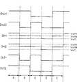
图6是示例说明图3的同时双向I/O电路的操作的时序图。现在,将参考图3、4和6描述图3的同时双向I/O电路的操作。FIG. 6 is a timing diagram illustrating the operation of the simultaneous bidirectional I/O circuit of FIG. 3 . Now, the operation of the simultaneous bidirectional I/O circuit of FIG. 3 will be described with reference to FIGS. 3 , 4 and 6 .
在时间片A中,因为从输入端310接收的即使传送的输出信号Dout为逻辑高,启动第一信号检测电路360,以及停止第二信号检测电路380。由于晶体管361和381的操作,将即使传送的输出信号Dout用作选择信号以便启动第一信号检测电路360或第二信号检测电路380。In time slice A, since the transmitted output signal Dout received from the
如果从来自引脚340的同时双向检测电路300的外部接收的输入信号IN为逻辑高,总线330上的信号Din的电平与第一基准电压VrefH相同。因此,差分放大器369放大总线330上的电压Din与第二基准电压VrefM间的差值,并将所放大的差分信号输出给第一和第二输出端OUT和OUTB。差分放大器371也是有效的,因为放大器371的两个输入具有相同的输入电平(等于VrefH的Din,以及信号VrefH本身),放大器372的输出将不影响差分放大器369的输出。此时,第一输入端OUT的输出信号处于逻辑高状态,如图6的时间片A所示。If the input signal IN received from the outside of the simultaneous
在时间片B,即将传送的输出信号Dout具有逻辑高电平,以及输入信号IN具有逻辑低电平。因此,总线330上的电压Din与逻辑高电平和逻辑低电平之和的中间电平相同,即,第二基准电压VrefM。因为Dout仍然为高,第一信号检测电路360仍然有效。因此,差分放大器371放大总线330上的电压Din(=VrefM)和第一基准电压VrefH间的差值,并将所放大的差分信号输出给第一和第二输出端OUT和OUTB。差分放大器369的输入均等于VrefM,以致放大器369不影响输出线OUT和OUTB。此时,用于第一输出端OUT的输出信号处于逻辑低状态。In time slice B, the output signal Dout to be transmitted has a logic high level, and the input signal IN has a logic low level. Therefore, the voltage Din on the
在时间片C,即将传送的输出信号Dout具有逻辑低电平,以及输入信号IN具有逻辑高电平。因为Dout为低,由于晶体管361和381的操作,停止第一信号检测电路360,以及启动第二信号检测电路380。如图6的时间片C所示,总线330上的信号Din的电压电平为即使传送的输出信号Dout的逻辑低电平和输入信号IN的逻辑高电平之和的中间值,即,第二基准电压VrefM。In time slice C, the output signal Dout to be transmitted has a logic low level, and the input signal IN has a logic high level. Since Dout is low, the first
因此,差分放大器391放大总线330上的电压Din(=VrefM)和第三基准电压VrefL间的差值,并将所放大的差分信号输出给第一和第二输出端OUT和OUTB。如在上述例子中,差分放大器389不影响输出端OUT和OUTB的输出,因为放大器389的输入没有差别。在这里,第一输出端OUT的输出信号为逻辑高电平。Therefore, the differential amplifier 391 amplifies the difference between the voltage Din (=VrefM) on the
如图6的时间片D所示,即将传送的输出信号Dout具有逻辑低电平,以及输入信号IN还具有逻辑低电平。因为Dout为低,停止第一信号检测电路360,以及启动第二信号检测电路380。总线330上的信号Din的电压电平变为第三基准电压VrefL,VrefL为逻辑低,因为信号Dout和IN均为低。As shown in time slice D of FIG. 6 , the output signal Dout to be transmitted has a logic low level, and the input signal IN also has a logic low level. Since Dout is low, the first
因此,差分放大器389放大总线330上的电压Din(=VrefL)和第二基准电压VrefM间的差值并将所放大的差分信号提供给第一和第二输出端OUT和OUTB。如上,差分放大器391不影响差分放大器389的输出信号。此时,第一输出端OUT的第一输出信号具有逻辑低电平。Therefore, the differential amplifier 389 amplifies the difference between the voltage Din (=VrefL) on the
基于图3、5和6的同时双向I/O电路300的操作与上面已经描述过的基于图3、4和6的同时双向I/O电路300的操作相同。因此,将不详细地描述参考那些图的操作。The operation of the simultaneous bidirectional I/
如上所述,根据本发明的实施例的同时双向I/O电路300能检测具有50%摆幅容限(swing margin)的输入数据IN。换句话说,对输入到I/O电路300的信号的每个组合来说,输入缓冲器350中的至少一个差分放大器将输入信号IN将高于或低于IN值50%的基准电压进行比较。As described above, the simultaneous bidirectional I/
图7是根据本发明的实施例,包括两个同时双向I/O电路300的数据传输系统的示意框图。参考图7,数据传输系统700包括第一同时双向I/O电路300、第二同时双向I/O电路300′,以及连接两个I/O电路的系统总线(或通道)750。能在单独的半导体设备中形成I/O电路300、300′。FIG. 7 is a schematic block diagram of a data transmission system including two simultaneous bidirectional I/
容纳I/O电路300、300′的半导体器件,每个能包括连接一个或多个半导体器件中的其他I/O电路的多个同时双向I/I电路。操作中,能并联同时双向I/O电路以便它们能在其他相应的系统总线上并行地将数据传送到彼此和并联地从彼此接受数据。The semiconductor devices housing the I/
然而,为了方便,图7仅表示第一和第二同时双向I/O电路300、300′和一条系统总线750。However, for convenience, only the first and second simultaneous bidirectional I/
第一同时双向I/O电路300包括第一输出缓冲器320和第一输入缓冲器350,以及第二同时双向I/O电路300′包括第二输出缓冲器320′和第二输入缓冲器350′。第二同时双向I/O电路300′的结构和操作与图3的同时双向I/O电路300相同。The first simultaneous bidirectional I/
图8是示例说明图7中所示的数据传输系统的操作的时序图。现在将参考图4、7和8描述数据传输系统700的操作。FIG. 8 is a sequence diagram illustrating the operation of the data transmission system shown in FIG. 7 . The operation of the
首先,如果从引脚310接收的数据Dout1和从引脚310′接收的数据Dout2为逻辑高状态,如图的8的时间片A所示,第一和第二输出缓冲器320和320′分别将逻辑高数据Dout1和Dout2输出到相应的总线330和330′。First, if the data Dout1 received from the
如参考图4所述,因为Dout1和Dout2均为高,启动第一和第二输入缓冲器350和350′的每一个的第一信号检测电路360,以及停止第一和第二输入缓冲器350和350′的每一个的第二信号检测电路380。因此,第一输入缓冲器350接收第二基准电压VrefM和总线330上的数据Din1,放大它们之间的差值,以及检测逻辑高状态中的数据OUT1(=Dout2)。第二输入缓冲器350′接收第二基准电压VrefM和总线330′上的数据Din2,放大它们之间的差值,并检测逻辑高状态中的数据OUT2(=Dout1)。As described with reference to FIG. 4, since both Dout1 and Dout2 are high, the first
如果从引脚310接收的数据Dout1为逻辑高状态以及从引脚310′接收的数据Dout2为逻辑低状态,如图8的时间片B所示,总线330和330′上的数据Din1和Din2的电平分别具有逻辑高电平和逻辑低电平的中间值。If the data Dout1 received from the
基于即将传送的信号Dout1,分别启动和停止第一输入缓冲器350的第一和第二信号检测电路360和380。因此,第一输入缓冲器350接收第一基准电压VrefH和总线330上的数据Din1,放大它们之间的差值,以及检测从第二输出缓冲器320′输出的逻辑低状态中的数据OUT1(=Dout2)。Based on the signal Dout1 to be transmitted, the first and second
分别启动和停止第二输入缓冲器350′的第一和第二信号检测电路360和380。因此,第二输入缓冲器350′接收第三基准电压VrefL以及总线330′上的数据Din2,放大它们之间的差值,并检测从第一输入输出缓冲器320输出的逻辑高状态中的数据OUT2(=Dout1)。The first and second
如果从引脚310接收的数据Dout1处于逻辑低状态,以及从引脚310′接收的数据Dout2处于逻辑高状态,如图8的时间片C所示,总线330和330′上的数据Din1和Din2的电平分别具有逻辑高电平和逻辑低电平的中间值。即,Din1=Din2=(Dout1+Dout2)/2。If the data Dout1 received from the
如参考图4所述,启动第一输入缓冲器350的第一和第二信号检测电路360和380。因此,第一输入缓冲器350接收第三基准电压VrefL和总线330上的数据Din1,放大它们间的差值,并检测从第二输出缓冲器320’输出的逻辑高状态中的数据OUT1(=Dout2)。As described with reference to FIG. 4 , the first and second
分别启动和停止第二输入缓冲器350’的第一和第二信号检测电路360和380。因此,第二输入缓冲器350’接收第一基准电压VrefH以及总线330’上的数据Din2,放大它们间的差值,并检测从第一输出缓冲器320输出的逻辑低状态中的数据OUT2(=Dout1)。The first and second
图8中的剩余时间片D、E和F中的第一和第二同时双向I/O电路300、300’的操作如参考图3、4和6所述。The operation of the first and second simultaneous bidirectional I/
因此,包括根据本发明的实施例的同时双向I/O电路的系统检测具有约50%的摆幅容限的输入数据,以致其比传统电路更少受噪声、功率或其他干扰的影响。如上所述,通过使用三个基准电压和即将传送的输出信号的组合,所检测的每个输入信号具有约50%的摆幅容限。Therefore, a system including a simultaneous bidirectional I/O circuit according to an embodiment of the present invention detects input data with about 50% swing margin, so that it is less affected by noise, power, or other disturbances than conventional circuits. As mentioned above, by using a combination of three reference voltages and the output signal to be transmitted, each input signal detected has about 50% swing margin.
尽管已经参考优选实施例,具体示出和描述了本发明,但是本领域的普通技术人员将理解到,在不脱离由附加权利要求书限定的本发明的精神和范围的情况下,可在形式和细节方面做出各种改变。While the present invention has been particularly shown and described with reference to preferred embodiments, it will be understood by those skilled in the art that changes may be made in the form of and various changes in details.
Claims (30)
Applications Claiming Priority (4)
| Application Number | Priority Date | Filing Date | Title |
|---|---|---|---|
| KR1020020058120AKR100891322B1 (en) | 2002-09-25 | 2002-09-25 | Simultaneous bi-directional I / O circuit to improve data input margin |
| KR58120/2002 | 2002-09-25 | ||
| US10/379,781 | 2003-03-04 | ||
| US10/379,781US7102545B2 (en) | 2002-09-25 | 2003-03-04 | Simultaneous bidirectional input/output circuit |
Publications (2)
| Publication Number | Publication Date |
|---|---|
| CN1497413Atrue CN1497413A (en) | 2004-05-19 |
| CN100339802C CN100339802C (en) | 2007-09-26 |
Family
ID=31980694
Family Applications (1)
| Application Number | Title | Priority Date | Filing Date |
|---|---|---|---|
| CNB031598218AExpired - LifetimeCN100339802C (en) | 2002-09-25 | 2003-09-25 | Simultaneous two-way input/output circuit |
Country Status (3)
| Country | Link |
|---|---|
| EP (1) | EP1404050B1 (en) |
| JP (1) | JP4444608B2 (en) |
| CN (1) | CN100339802C (en) |
Cited By (2)
| Publication number | Priority date | Publication date | Assignee | Title |
|---|---|---|---|---|
| CN103199845A (en)* | 2012-01-09 | 2013-07-10 | 上海华虹集成电路有限责任公司 | Two-way buffer based on open-drain bus |
| CN106649171A (en)* | 2016-09-21 | 2017-05-10 | 上海华虹计通智能系统股份有限公司 | Single-bus full-duplex data communication method and system |
Families Citing this family (2)
| Publication number | Priority date | Publication date | Assignee | Title |
|---|---|---|---|---|
| KR100532433B1 (en)* | 2003-05-07 | 2005-11-30 | 삼성전자주식회사 | Apparatus and method for inputting/outputting data simultaneously through a single pad |
| JP4977056B2 (en)* | 2008-02-20 | 2012-07-18 | 株式会社アドバンテスト | Test equipment |
Family Cites Families (6)
| Publication number | Priority date | Publication date | Assignee | Title |
|---|---|---|---|---|
| GB2230165B (en)* | 1989-03-30 | 1993-09-15 | Plessey Co Plc | High speed asynchronous data interface |
| DE69211584T2 (en)* | 1991-03-14 | 1996-10-31 | Bull Sa | Method and circuit for transmission detection for bidirectional, differential route |
| FR2746946B1 (en) | 1996-03-29 | 1998-12-31 | Valeo Equip Electr Moteur | SYSTEM OF SIMULTANEOUS TWO-WAY COMMUNICATION BETWEEN TWO ELECTRIC OR ELECTRONIC COMPONENTS OF A MOTOR VEHICLE, AND MEMBER EQUIPPED WITH CORRESPONDING MEANS |
| US6127849A (en)* | 1998-08-11 | 2000-10-03 | Texas Instruments Incorporated | Simultaneous bi-directional input/output (I/O) circuit |
| US6158027A (en)* | 1998-08-31 | 2000-12-05 | International Business Machines Corporation | Enhanced noise-predictive maximum likelihood (NPML) data detection method and apparatus for direct access storage device (DASD) |
| DE10113822A1 (en)* | 2000-10-02 | 2002-04-25 | Fujitsu Ltd | Receiver, hybrid circuit, control circuit and signal transmission system for bidirectional signal transmission for simultaneous execution of such a signal transmission in both directions |
- 2003
- 2003-09-23EPEP03255952Apatent/EP1404050B1/ennot_activeExpired - Lifetime
- 2003-09-24JPJP2003332217Apatent/JP4444608B2/ennot_activeExpired - Fee Related
- 2003-09-25CNCNB031598218Apatent/CN100339802C/ennot_activeExpired - Lifetime
Cited By (4)
| Publication number | Priority date | Publication date | Assignee | Title |
|---|---|---|---|---|
| CN103199845A (en)* | 2012-01-09 | 2013-07-10 | 上海华虹集成电路有限责任公司 | Two-way buffer based on open-drain bus |
| CN103199845B (en)* | 2012-01-09 | 2017-03-15 | 上海华虹集成电路有限责任公司 | Bidirectional buffer based on open drain bus |
| CN106649171A (en)* | 2016-09-21 | 2017-05-10 | 上海华虹计通智能系统股份有限公司 | Single-bus full-duplex data communication method and system |
| CN106649171B (en)* | 2016-09-21 | 2020-05-05 | 上海华虹计通智能系统股份有限公司 | Single-bus full-duplex data communication method and system |
Also Published As
| Publication number | Publication date |
|---|---|
| EP1404050A2 (en) | 2004-03-31 |
| EP1404050B1 (en) | 2011-11-09 |
| JP4444608B2 (en) | 2010-03-31 |
| EP1404050A3 (en) | 2005-11-30 |
| JP2004118845A (en) | 2004-04-15 |
| CN100339802C (en) | 2007-09-26 |
Similar Documents
| Publication | Publication Date | Title |
|---|---|---|
| KR100744141B1 (en) | Virtual differential interconnect circuit and virtual differential signaling scheme for single-ended signal lines | |
| US8848810B2 (en) | Multiple transmitter system and method | |
| CN1921307A (en) | Dual reference input receiver of semiconductor device and method of receiving input data signal | |
| CN109032856A (en) | Execute the serial communication interface circuit and electronic device of external loop test | |
| JP4818928B2 (en) | Method and apparatus for receiver detection on a PCI Express bus | |
| US10580466B2 (en) | Transmitting device using calibration circuit, semiconductor apparatus and system including the same | |
| CN100401636C (en) | Simultaneous bidirectional input/output circuit and method | |
| CN1574672A (en) | Data transfer apparatus for low voltage differential signaling | |
| US8443125B2 (en) | Single pin read-write method and interface | |
| US7218136B2 (en) | Transmission circuit, data transfer control device and electronic equipment | |
| CN1694253A (en) | Semiconductor memory device with on-chip termination circuit | |
| US8575961B2 (en) | Multi-valued driver circuit | |
| KR20120076436A (en) | Semiconductor integrated circuit | |
| CN110364218B (en) | Integrated circuit chip and semiconductor device including same | |
| CN1497413A (en) | Simultaneous bidirectional input/output circuit | |
| TWI511454B (en) | Low voltage differential signal driving circuit and electronic device compatible with wired transmission | |
| TWI221295B (en) | Circuit for calibrating output driving of dram and method thereof | |
| US20040059845A1 (en) | Simultaneous bidirectional input/output circuit | |
| CN106951382B (en) | LVDS receiving circuit supporting DDR data format | |
| CN1681207A (en) | Output Driver with Adjustable Swing Width During Test Mode Operation | |
| CN1089505C (en) | Signal receiving and signal processing device | |
| KR20010102404A (en) | Bus Driver with Data Dependent Drive Strength Control Logic | |
| US20050174149A1 (en) | Device for generating a pair of true/complement-phase logic signals | |
| CN1630191A (en) | Input buffer and semiconductor device including the same | |
| JP3664953B2 (en) | Semiconductor integrated circuit device |
Legal Events
| Date | Code | Title | Description |
|---|---|---|---|
| C06 | Publication | ||
| PB01 | Publication | ||
| C10 | Entry into substantive examination | ||
| SE01 | Entry into force of request for substantive examination | ||
| C14 | Grant of patent or utility model | ||
| GR01 | Patent grant | ||
| CX01 | Expiry of patent term | ||
| CX01 | Expiry of patent term | Granted publication date:20070926 |