CN1492498A - Semiconductor device - Google Patents
Semiconductor deviceDownload PDFInfo
- Publication number
- CN1492498A CN1492498ACNA021233454ACN02123345ACN1492498ACN 1492498 ACN1492498 ACN 1492498ACN A021233454 ACNA021233454 ACN A021233454ACN 02123345 ACN02123345 ACN 02123345ACN 1492498 ACN1492498 ACN 1492498A
- Authority
- CN
- China
- Prior art keywords
- signal
- power supply
- wiring
- solder joint
- earthy
- Prior art date
- Legal status (The legal status is an assumption and is not a legal conclusion. Google has not performed a legal analysis and makes no representation as to the accuracy of the status listed.)
- Granted
Links
Images


Classifications
- H—ELECTRICITY
- H01—ELECTRIC ELEMENTS
- H01L—SEMICONDUCTOR DEVICES NOT COVERED BY CLASS H10
- H01L23/00—Details of semiconductor or other solid state devices
- H01L23/48—Arrangements for conducting electric current to or from the solid state body in operation, e.g. leads, terminal arrangements ; Selection of materials therefor
- H01L23/50—Arrangements for conducting electric current to or from the solid state body in operation, e.g. leads, terminal arrangements ; Selection of materials therefor for integrated circuit devices, e.g. power bus, number of leads
- H—ELECTRICITY
- H01—ELECTRIC ELEMENTS
- H01L—SEMICONDUCTOR DEVICES NOT COVERED BY CLASS H10
- H01L23/00—Details of semiconductor or other solid state devices
- H01L23/48—Arrangements for conducting electric current to or from the solid state body in operation, e.g. leads, terminal arrangements ; Selection of materials therefor
- H01L23/488—Arrangements for conducting electric current to or from the solid state body in operation, e.g. leads, terminal arrangements ; Selection of materials therefor consisting of soldered or bonded constructions
- H01L23/498—Leads, i.e. metallisations or lead-frames on insulating substrates, e.g. chip carriers
- H01L23/49838—Geometry or layout
- H—ELECTRICITY
- H01—ELECTRIC ELEMENTS
- H01L—SEMICONDUCTOR DEVICES NOT COVERED BY CLASS H10
- H01L2224/00—Indexing scheme for arrangements for connecting or disconnecting semiconductor or solid-state bodies and methods related thereto as covered by H01L24/00
- H01L2224/01—Means for bonding being attached to, or being formed on, the surface to be connected, e.g. chip-to-package, die-attach, "first-level" interconnects; Manufacturing methods related thereto
- H01L2224/42—Wire connectors; Manufacturing methods related thereto
- H01L2224/47—Structure, shape, material or disposition of the wire connectors after the connecting process
- H01L2224/48—Structure, shape, material or disposition of the wire connectors after the connecting process of an individual wire connector
- H01L2224/481—Disposition
- H01L2224/48151—Connecting between a semiconductor or solid-state body and an item not being a semiconductor or solid-state body, e.g. chip-to-substrate, chip-to-passive
- H01L2224/48221—Connecting between a semiconductor or solid-state body and an item not being a semiconductor or solid-state body, e.g. chip-to-substrate, chip-to-passive the body and the item being stacked
- H01L2224/48225—Connecting between a semiconductor or solid-state body and an item not being a semiconductor or solid-state body, e.g. chip-to-substrate, chip-to-passive the body and the item being stacked the item being non-metallic, e.g. insulating substrate with or without metallisation
- H01L2224/48235—Connecting between a semiconductor or solid-state body and an item not being a semiconductor or solid-state body, e.g. chip-to-substrate, chip-to-passive the body and the item being stacked the item being non-metallic, e.g. insulating substrate with or without metallisation connecting the wire to a via metallisation of the item
- H—ELECTRICITY
- H01—ELECTRIC ELEMENTS
- H01L—SEMICONDUCTOR DEVICES NOT COVERED BY CLASS H10
- H01L24/00—Arrangements for connecting or disconnecting semiconductor or solid-state bodies; Methods or apparatus related thereto
- H01L24/01—Means for bonding being attached to, or being formed on, the surface to be connected, e.g. chip-to-package, die-attach, "first-level" interconnects; Manufacturing methods related thereto
- H01L24/42—Wire connectors; Manufacturing methods related thereto
- H01L24/47—Structure, shape, material or disposition of the wire connectors after the connecting process
- H01L24/48—Structure, shape, material or disposition of the wire connectors after the connecting process of an individual wire connector
- H—ELECTRICITY
- H01—ELECTRIC ELEMENTS
- H01L—SEMICONDUCTOR DEVICES NOT COVERED BY CLASS H10
- H01L2924/00—Indexing scheme for arrangements or methods for connecting or disconnecting semiconductor or solid-state bodies as covered by H01L24/00
- H01L2924/0001—Technical content checked by a classifier
- H01L2924/00014—Technical content checked by a classifier the subject-matter covered by the group, the symbol of which is combined with the symbol of this group, being disclosed without further technical details
- H—ELECTRICITY
- H01—ELECTRIC ELEMENTS
- H01L—SEMICONDUCTOR DEVICES NOT COVERED BY CLASS H10
- H01L2924/00—Indexing scheme for arrangements or methods for connecting or disconnecting semiconductor or solid-state bodies as covered by H01L24/00
- H01L2924/15—Details of package parts other than the semiconductor or other solid state devices to be connected
- H01L2924/151—Die mounting substrate
- H01L2924/1517—Multilayer substrate
- H01L2924/15172—Fan-out arrangement of the internal vias
- H01L2924/15173—Fan-out arrangement of the internal vias in a single layer of the multilayer substrate
- H—ELECTRICITY
- H01—ELECTRIC ELEMENTS
- H01L—SEMICONDUCTOR DEVICES NOT COVERED BY CLASS H10
- H01L2924/00—Indexing scheme for arrangements or methods for connecting or disconnecting semiconductor or solid-state bodies as covered by H01L24/00
- H01L2924/15—Details of package parts other than the semiconductor or other solid state devices to be connected
- H01L2924/151—Die mounting substrate
- H01L2924/153—Connection portion
- H01L2924/1531—Connection portion the connection portion being formed only on the surface of the substrate opposite to the die mounting surface
- H01L2924/15311—Connection portion the connection portion being formed only on the surface of the substrate opposite to the die mounting surface being a ball array, e.g. BGA
- H—ELECTRICITY
- H01—ELECTRIC ELEMENTS
- H01L—SEMICONDUCTOR DEVICES NOT COVERED BY CLASS H10
- H01L2924/00—Indexing scheme for arrangements or methods for connecting or disconnecting semiconductor or solid-state bodies as covered by H01L24/00
- H01L2924/19—Details of hybrid assemblies other than the semiconductor or other solid state devices to be connected
- H01L2924/1901—Structure
- H01L2924/1904—Component type
- H01L2924/19041—Component type being a capacitor
- H—ELECTRICITY
- H01—ELECTRIC ELEMENTS
- H01L—SEMICONDUCTOR DEVICES NOT COVERED BY CLASS H10
- H01L2924/00—Indexing scheme for arrangements or methods for connecting or disconnecting semiconductor or solid-state bodies as covered by H01L24/00
- H01L2924/30—Technical effects
- H01L2924/301—Electrical effects
- H01L2924/30107—Inductance
- H—ELECTRICITY
- H01—ELECTRIC ELEMENTS
- H01L—SEMICONDUCTOR DEVICES NOT COVERED BY CLASS H10
- H01L2924/00—Indexing scheme for arrangements or methods for connecting or disconnecting semiconductor or solid-state bodies as covered by H01L24/00
- H01L2924/30—Technical effects
- H01L2924/301—Electrical effects
- H01L2924/3011—Impedance
Landscapes
- Physics & Mathematics (AREA)
- Condensed Matter Physics & Semiconductors (AREA)
- General Physics & Mathematics (AREA)
- Engineering & Computer Science (AREA)
- Computer Hardware Design (AREA)
- Microelectronics & Electronic Packaging (AREA)
- Power Engineering (AREA)
- Geometry (AREA)
- Wire Bonding (AREA)
- Semiconductor Integrated Circuits (AREA)
Abstract
Translated fromChinese
Description
Translated fromChinese技术领域technical field
本发明涉及半导体器件及利用其的电子装置,特别是涉及超高速工作或者超高集成度的半导体器件及利用其的电子装置。The present invention relates to a semiconductor device and an electronic device using the same, in particular to an ultra-high-speed operation or ultra-high integration semiconductor device and an electronic device using the same.
背景技术Background technique
电子电路和电子装置的进步是惊人的,特别是最近几年,其工作速度和集成化不断地显著提高。一旦电子装置高速化,则能简便廉价的实现各种处理。此外,由于提高了集成度,可能实现复杂的功能。这种倾向对于半导体器件特别显著。这样,由于电子电路、电子装置和半导体器件工作速度的提高和高集成化,促进了电子工业的进步和发展。The progress of electronic circuits and electronic devices is astonishing, especially in recent years, the speed of operation and integration of which have continued to increase significantly. Once the speed of electronic devices is increased, various processes can be realized simply and inexpensively. In addition, complex functions are possible due to increased integration. This tendency is particularly remarkable for semiconductor devices. In this way, the progress and development of the electronics industry has been promoted due to the increase in operating speed and high integration of electronic circuits, electronic devices and semiconductor devices.
半导体元件高集成化,内含电路数增加,由于要和其半导体元件等相连,所以增加必要的管脚数。解决这问题的一种方法,由美国专利5216278的说明书公开,采用BGA封装方法。把半导体元件封装在BGA封装内,制成BGA型半导体器件。Semiconductor elements are highly integrated, and the number of included circuits increases. Since it needs to be connected with other semiconductor elements, the number of necessary pins increases. A method for solving this problem, disclosed by the specification of US Patent No. 5,216,278, adopts a BGA packaging method. The semiconductor element is packaged in the BGA package to make a BGA type semiconductor device.
下面结合附图,说明现有的BGA型半导体器件。The existing BGA type semiconductor device will be described below with reference to the accompanying drawings.
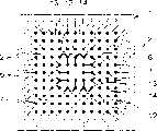
图9是BGA型半导体器件使用的BGA基板的上面图。BGA基板1是由有机材料的印刷板和陶瓷印刷基板组成的布线板。BGA基板1的中央部分是装载半导体元件的位置5,在这里设置半导体元件。焊点4是设置在BGA基板1上的用来焊接的焊点。焊点4和半导体元件上的电极通过焊接引线相互电连接。从焊点4布线图形大致放射状地延伸,在布线图形3的端部和通孔2相连接。在BGA基板的中央部分、布线图形3的密度高,为了避免高密度,在BGA基板1的外围设置通孔2。Fig. 9 is a top view of a BGA substrate used in a BGA type semiconductor device. The
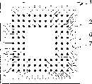
图10是BGA基板1的背面图。通孔2连接正反面的布线。在BGA基板1的背面,来自通孔2的布线6延伸,和焊点7相连。焊点7按二维排列。即,如图10所示的例子,三排焊点沿四周排列、不是排成1排,而是保持等宽的二维排列。FIG. 10 is a rear view of the
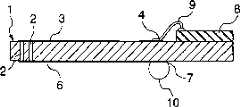
图11是把半导体元件8放置在BGA基板1上时,BGA基板1的主要部分剖视图。半导体元件8上的电极和BGA基板上的焊点4通过焊接引线9相互连接。从焊点4来的布线,经过布线图形3到通孔2。再到布线图形6,最后到焊点7。在焊点7与焊球10等连接。图中虽没有表示,但该BGA型半导体器件通过该焊球10等安装连接在印刷电路板等上,使与其他半导体等电连接。FIG. 11 is a cross-sectional view of main parts of the
上述BGA半导体器件的特征是,和诸如DIP(双列直插式封装)和QFP(四面封装)等的封装相比,对于相同的外形尺寸,包括的管脚数可能多。这样,如图10所示由于焊点7按二维结构设置,其他封装不具有特征。多亏半导体元件高密度化,增加内部包含的电路数,即使增加管脚数,也能制造外形尺寸不大的半导体器件,为电子工业的进步和发展作出贡献。A feature of the above-mentioned BGA semiconductor device is that, compared with packages such as DIP (Dual In-line Package) and QFP (Quad Package), the number of included pins may be larger for the same external size. In this way, as shown in FIG. 10, since the
但是,由于半导体器件工作速度进一步提高,或者集成度进一步增加,对于现有的BGA型半导体器件,有时不能再适应。However, due to the further improvement of the operating speed of the semiconductor device or the further increase of the degree of integration, the existing BGA type semiconductor device sometimes cannot be adapted.
对于使用半导体器件的重要事项是电源的噪声。一旦半导体器件工作则消耗电功率,但是消耗的电流因内部电路的工作而变动,所以按照电源系统布线具有的阻抗,产生电源噪声。如果电源噪声为ΔV,电源系统阻抗为Z,消耗电流变化为ΔI,则三者的关系由ΔV=Z×ΔI式来表示。An important matter for using semiconductor devices is the noise of the power supply. When a semiconductor device is in operation, electric power is consumed, but the consumed current fluctuates due to the operation of the internal circuit, so power supply noise is generated according to the impedance of the wiring of the power supply system. If the power supply noise is ΔV, the power system impedance is Z, and the consumption current change is ΔI, then the relationship between the three is expressed by the formula ΔV=Z×ΔI.
在半导体器件的情况,电源系统的阻抗由半导体器件内的布线电感L产生,如果半导体器件的工作频率为f,则该电源系统的阻抗Z由公式Z=2πfL确定。In the case of semiconductor devices, the impedance of the power system is generated by the wiring inductance L in the semiconductor device. If the operating frequency of the semiconductor device is f, the impedance Z of the power system is determined by the formula Z=2πfL.
在放置半导体器件的印刷电路板等中,通过分流电容器和平面状的电源和接地布线等,由于电源系统的阻抗被控制得低,所以电源系统整体阻抗的主要成分往往是半导体器件内布线的电感L。In printed circuit boards, etc. where semiconductor devices are placed, the impedance of the power system is controlled to be low through shunt capacitors and planar power and ground wiring, etc., so the main component of the overall impedance of the power system is often the inductance of the wiring in the semiconductor device. L.
因此,电源噪声ΔV,用公式ΔV=2πfL×ΔI表示,由工作频率f,半导体器件内布线电感L,消耗电流变动成分ΔI决定。Therefore, the power supply noise ΔV, expressed by the formula ΔV=2πfL×ΔI, is determined by the operating frequency f, the wiring inductance L of the semiconductor device, and the consumption current fluctuation component ΔI.
如果该电源噪声过大,则半导体器件误动作。这是由于,电源电压超出半导体器件中电路的正常工作范围,电源噪声重叠在信号线上,使其电路产生误动作的缘故。这样,如果电源噪声不能抑制在规定值以内,则使半导体器件误动作,使其不能使用。If the power supply noise is too large, the semiconductor device malfunctions. This is because the power supply voltage exceeds the normal operating range of the circuit in the semiconductor device, and power supply noise is superimposed on the signal line, causing the circuit to malfunction. In this way, if the power supply noise cannot be suppressed within a predetermined value, the semiconductor device may malfunction and become unusable.
如果半导体器件的工作频率提高,按照以前表示式ΔV=2πfL×ΔI,则电源噪声增大,半导体器件产生误动作,有时不能使用半导体器件。If the operating frequency of the semiconductor device is increased, according to the previous expression ΔV=2πfL×ΔI, the noise of the power supply will increase, the semiconductor device will malfunction, and sometimes the semiconductor device cannot be used.
并且,半导体器件高集成化,内含电路数增加,结果消耗电流增大,消耗电流变化ΔI增大,所以按照以前表达式ΔV=2πfL×ΔI,电源噪声增大,半导体器件发生误动作,有时不能使用半导体器件。In addition, semiconductor devices are highly integrated, and the number of built-in circuits increases. As a result, the current consumption increases, and the change in consumption current ΔI increases. Therefore, according to the previous expression ΔV=2πfL×ΔI, power supply noise increases, and semiconductor devices malfunction, sometimes Semiconductor devices cannot be used.
还有,半导体器件工作频率f提高,特别是CMOS型半导体器件,消耗电流与频率成比例的增大结果消耗电流变动ΔI增大,按照前述表达式ΔV=2πfL×ΔI,则电源噪声增大,半导体器件产生误动作,有时不能使用半导体器件。In addition, the operating frequency f of semiconductor devices is increased, especially for CMOS type semiconductor devices, the increase in the consumption current proportional to the frequency results in an increase in the consumption current variation ΔI. According to the aforementioned expression ΔV=2πfL×ΔI, the power supply noise increases, The semiconductor device malfunctions, and sometimes the semiconductor device cannot be used.
用图9到图11所示的现有技术中的实施例来说明这些情况。These cases are illustrated with the prior art embodiments shown in FIGS. 9 to 11 .
如图9到图11所示,布线图形3和布线图形6的线宽度为0.15mm,两种线的长度都为5mm。通孔2的直径0.3mm,长度(深度)为0.8mm。此外,焊接引线9的直径为0.04mm,长度为2mm。As shown in FIGS. 9 to 11, the
对于这种构造,BGA基板部的布线电感,即,由布线图形3与布线图形6和通孔2构成的布线电感为5.1nH,焊接引线部的电感为1.7nH,两者合计为6.8nH。对于现有的BGA型半导体器件,电源用的布线5条,地线用的布线5条,所以总的电感Lo=(6.8nH/5)+(6.8nH/5)=2.72nH。象这样,已有的BGA型半导体器件内电源系统布线电感Lo是2.72nH。With this structure, the wiring inductance of the BGA substrate portion, that is, the wiring inductance of the
如上所述的现有BGA型半导体器件,如果工作频率为110MHz,消耗电流变化ΔI为0.5A,则正常工作。因为这时,BGA型半导体器件的电源噪声ΔV,由表达式ΔV=2π110MHz×2.72nH×0.5A=0.94V表示,在许可的电源噪声1V之内。因此,在上所述的现有BGA型半导体器件,上述条件,即界限是工作频率110MHz,消耗电流变化ΔI为0.5A。The conventional BGA type semiconductor device as described above works normally if the operating frequency is 110 MHz and the change in consumption current ΔI is 0.5 A. Because at this time, the power supply noise ΔV of the BGA type semiconductor device is represented by the expression ΔV=2π110MHz×2.72nH×0.5A=0.94V, which is within the allowable power supply noise 1V. Therefore, in the above-mentioned conventional BGA type semiconductor device, the above-mentioned conditions, that is, the limit is that the operating frequency is 110 MHz, and the change in consumption current ΔI is 0.5 A.
而且,如图9到图11所示的现有的BGA型半导体器件,工作频率进一步提高,或者,消耗电流变化进一步增大,则电源噪声超过许可值,产生误动作,其不能被使用。Moreover, the conventional BGA type semiconductor devices shown in FIGS. 9 to 11, if the operating frequency is further increased, or if the variation of the consumption current is further increased, the noise of the power supply exceeds the allowable value, resulting in malfunction, and it cannot be used.
这样一来,如半导体器件工作速度进一步提高,或者集成度进一步增大,现有的BGA型半导体器件。有时不能适应。In this way, if the operating speed of the semiconductor device is further improved, or the degree of integration is further increased, the existing BGA type semiconductor device. Sometimes can not adapt.
发明内容Contents of the invention
因此,本发明要解决的技术问题是克服上述现有技术中存在的问题,其目的在于获得具有超高速度,或者超高集成度的BGA型半导体器件或者电子装置。Therefore, the technical problem to be solved by the present invention is to overcome the problems existing in the above-mentioned prior art, and its purpose is to obtain a BGA-type semiconductor device or electronic device with ultra-high speed or ultra-high integration.
按照本发明的BGA型半导体器件,为了解决上述问题,达到上述目的,在设置半导体器件内电源系统的布线时,把它的布线,特别是所谓信号线进行分别设置,通过缩短电源系统的布线长度,或者通过增加电源系统的布线条数、降低电源系统的电感,能适应半导体器件的进一步提高工作速度或者进一步增加集成度的情况。According to the BGA type semiconductor device of the present invention, in order to solve the above-mentioned problems and achieve the above-mentioned purpose, when arranging the wiring of the power supply system in the semiconductor device, its wiring, especially the so-called signal lines, are respectively arranged, by shortening the wiring length of the power supply system , or by increasing the number of wiring lines of the power system and reducing the inductance of the power system, it can adapt to the situation of further increasing the working speed of semiconductor devices or further increasing the degree of integration.
即,按照本发明的半导体器件,是具有基板和在该基板上面设有半导体芯片以及在该基板下面设有多个焊点的半导体器件,该基板在基板的外围部分具有连接半导体芯片信号用布线的第1通孔群,在该基板装载半导体芯片位置的周围具有连接半导体芯片电源线或地线的第2通孔群。That is, according to the semiconductor device of the present invention, it is a semiconductor device that has a substrate, a semiconductor chip is provided on the upper surface of the substrate, and a plurality of pads are provided on the lower surface of the substrate, and the substrate has wiring for connecting the semiconductor chip signal at the peripheral portion of the substrate. The first through-hole group has a second through-hole group connected to a power line or a ground line of the semiconductor chip around the position where the semiconductor chip is mounted on the substrate.
因此,电源系统布线的长度比信号用布线短,或增加电源系统的个数,其作用是降低电感。Therefore, the length of the power system wiring is shorter than that of the signal wiring, or the number of power supply systems is increased to reduce the inductance.
这样,在前述基板上,设置第1焊点,通过引线焊接来连接前述半导体芯片的信号用端子和前述信号用布线,设置第2焊点,通过引线焊接点来连接前述半导体芯片的电源或地线端和前述的电源或地线用的布线,前述的第二焊点可以设置在前述第1焊接点和前述半导体芯片之间。如果这样地设置焊点、则不影响布线图形、可以形成电源或者地线用的第2通孔,可以高密度地进行封装。In this way, on the above-mentioned substrate, the first pad is provided, and the signal terminal of the aforementioned semiconductor chip is connected to the above-mentioned signal wiring by wire bonding, and the second pad is provided, and the power supply or ground of the aforementioned semiconductor chip is connected by wire bonding. The wiring for the terminal and the aforementioned power supply or ground, and the aforementioned second pad may be provided between the aforementioned first pad and the aforementioned semiconductor chip. If the pads are provided in this way, second via holes for power supply or ground can be formed without affecting the wiring pattern, and high-density packaging can be performed.
这里,所谓基板的外围部分,在图1中用100表示,所谓装载半导体芯片位置周边,在图1用200表示。以后详细叙述图1。Here, the so-called peripheral portion of the substrate is denoted by 100 in FIG. 1 , and the so-called periphery of the semiconductor chip mounting position is denoted by 200 in FIG. 1 . Fig. 1 will be described in detail later.
在前述基板的1边长为a,前述半导体芯片1边长为b的情况,前述基板的外围部分是离前述基板外围为(a-b)/8的部分,前述装载半导体芯片位置的周边,最好是离前述半导体芯片装载位置的外周为(a-b)/8的部分。如果在其范围形成各自的通孔,电源系统布线的长度和信号用布线长度相比,可能是在其四分之一以内,则可以降低电感。In the case where the length of one side of the aforementioned substrate is a and the length of one side of the aforementioned semiconductor chip is b, the peripheral portion of the aforementioned substrate is a part that is (a-b)/8 from the outer periphery of the aforementioned substrate, and the periphery of the aforementioned semiconductor chip loading position is preferably It is a portion that is (a-b)/8 from the outer circumference of the aforementioned semiconductor chip loading position. If the respective via holes are formed in the range, the length of the power system wiring can be within a quarter of the length of the signal wiring, and the inductance can be reduced.
总之,本发明的半导体器件,由于把电源系统的布线设置在BGA基板的中央部分,电源系统布线长度比信号用布线短,或者增加电源系统的个数,其作用是减少电感。In short, in the semiconductor device of the present invention, since the wiring of the power supply system is arranged in the central part of the BGA substrate, the length of the wiring of the power supply system is shorter than that of the signal wiring, or the number of power supply systems is increased to reduce inductance.
此外,如果把按照本发明的半导体器件用于电子装置,则能使电子装置本身高速化。Furthermore, if the semiconductor device according to the present invention is used in an electronic device, the speed of the electronic device itself can be increased.
附图说明Description of drawings
图1是按照本发明的实施例的BGA半导体器件用的BGA基板上面图。1 is a top view of a BGA substrate for a BGA semiconductor device according to an embodiment of the present invention.
图2是按照本发明实施例的BGA半导体器件用的BGA基板的背面图。图3是按照本发明实施例的装载半导体元件的BGA基板的要部剖视图。FIG. 2 is a rear view of a BGA substrate for a BGA semiconductor device according to an embodiment of the present invention. 3 is a cross-sectional view of an essential part of a BGA substrate on which a semiconductor element is mounted according to an embodiment of the present invention.
图4是按照本发明的BGA半导体器件用的BGA基板的上面图。Fig. 4 is a top view of a BGA substrate for a BGA semiconductor device according to the present invention.
图5是按照本发明的BGA半导体器件用的BGA基板的背面图。Fig. 5 is a rear view of a BGA substrate for a BGA semiconductor device according to the present invention.
图6是按照本发明实施例的装载半导体元件的BGA基板的要部剖视图。6 is a cross-sectional view of an essential part of a BGA substrate on which a semiconductor element is mounted according to an embodiment of the present invention.
图7是装载按照本发明的BGA半导体器件的电子装置的说明图。Fig. 7 is an explanatory view of an electronic device loaded with a BGA semiconductor device according to the present invention.
图8是装载本发明的BGA半导体器件的电子装置的说明图。FIG. 8 is an explanatory diagram of an electronic device incorporating the BGA semiconductor device of the present invention.
图9是现有技术的BGA半导体器件用的BGA基板的上面图。FIG. 9 is a top view of a conventional BGA substrate for a BGA semiconductor device.
图10是现有技术的BGA半导体器件用的BGA基板的背面图。Fig. 10 is a rear view of a conventional BGA substrate for a BGA semiconductor device.
图11是按照现有技术的装载半导体元件的BGA基板的要部剖视图。11 is a cross-sectional view of main parts of a BGA substrate on which a semiconductor element is mounted according to the prior art.
具体实施方式Detailed ways
下面,参照附图说明本发明。Hereinafter, the present invention will be described with reference to the drawings.
图1至图3是说明本发明第1实施例的BGA半导体器件的图,图1是BGA基板的上面图,图2是BGA基板的背面图,图3是在BGA基板上装载半导体元件的BGA基板的要部剖视图。1 to 3 are diagrams illustrating a BGA semiconductor device according to a first embodiment of the present invention. FIG. 1 is a top view of a BGA substrate, FIG. 2 is a rear view of a BGA substrate, and FIG. 3 is a BGA in which semiconductor elements are mounted on a BGA substrate. Cross-sectional view of the main part of the substrate.
在图1到图3中,标号1表示基板、2表示通孔、3表示布线图形,4表示焊点,5表示在BGA基板1中央部分装载半导体元件的位置,6表示布线图形,7表示焊点,8表示半导体元件,10表示焊球,11表示电源焊点,12表示通孔,13表示焊点,14表示布线图形,15和16表示焊接引线。In Fig. 1 to Fig. 3, the
如图1所示,在BGA基板1上面,与焊点4一起,设置0.15mm宽的布线图形3,在通孔2连接布线图形3。这些用于连接信号的布线(对于本发明所说的信号是指除电源,地线以外的全部信号,例如,包括测试所用的信号等)。在装载半导体元件位置5的附近,设置电源焊点11。这些焊点用来连接电源或者接地的布线。电源焊点11与通孔12相连。As shown in FIG. 1 , on the
如图2所示,在BGA基板1的背面,配置连接通孔2的布线图形6和连接布线图形6的焊点7,这些用于信号布线连接。在BGA基板1的背面中央部分,与连接上述通孔12的0.3mm宽的布线图形14一起,设置连接布线图形14的焊点13,这些用于连接电源或者接地的布线。电源系统的布线图形14,为了降低电感,要扩大线的宽度,并且,通孔12和焊点13,不是1对1的连结,而是由多条布线进行连接。As shown in FIG. 2, on the back surface of the
如图3所示,设在BGA基板1上的半导体元件8的电极(信号电极),通过焊接引线15和布线图形3连接,通过布线图形3→通孔2→布线图形6,连接焊点7。在焊点7连接焊球10等。这些用于连接信号的布线。在BGA基板1的中央部分,半导体元件8的电极(电源电极和接地电极)和电源焊点11,通过焊接引线16相互连接,通过电源焊点11→通孔12→布线图形14,和焊点13相连。在焊点13,和焊球10等相连。这些焊球用于连接电源或者接地的布线。As shown in Figure 3, the electrode (signal electrode) of the
对于本实施例的构造,把电源或接地的布线各分成8组,这样通过把放射状的信号用布线在内侧,不减少信号线的条数,也可以不把放射状布线用于电源或者接地,而通过增加信号用布线来实现。For the structure of this embodiment, the wiring for power supply or grounding is divided into 8 groups. By putting the radial signal wiring inside, the number of signal lines is not reduced, and the radial wiring can not be used for power supply or grounding, but This is achieved by adding wiring for signals.
按照第1实施例,电源或地的布线,通过来自半导体元件8的焊接引线16,在半导体元件8的最近和电源焊点11相连,从电源焊点11,经过通孔12,宽0.3mm长约2mm的布线14和电源及接地用的焊点13相连。由于布线长度短,电感小,在本第1实施例,电感为1.5nH。此外,焊接引线16,直径为0.4mm,长1.7mm,电感为1.4nH。因此,从半导体元件8到焊点13的1条布线的电感,总计为2.9nH。电源布线的焊接引线,通孔及布线由8组构成,接地焊接引线和通孔及布线也有8组,按照理论,总电感Lo=(2.9nH/8)+(2.9nH/8)=0.73nH,利用多条布线的结果,实际上电感为0.6nH。According to the first embodiment, the wiring of the power supply or the ground is connected to the
这样构成的本第1实施例,可能在工作频率500MHz,消耗电流变化ΔI为0.5A的情况下工作。即,电源噪声ΔV=2π 500MHz×0.6nH×0.5A=0.94V,允许电源噪声在1V以下。The first embodiment thus constituted can operate at an operating frequency of 500 MHz and a change in consumption current ΔI of 0.5 A. That is, the power supply noise ΔV = 2π 500MHz × 0.6nH × 0.5A = 0.94V, allowing the power supply noise to be below 1V.
此外,本发明第1实施例,可能在工作频率110MHz消耗电流变动Δ2.3A条件下工作。即,电源噪声ΔV=2π×110MHz×0.60nH×2.3A=0.95V,许可电源噪声在1V以内。In addition, the first embodiment of the present invention may work under the condition of a current consumption fluctuation of Δ2.3A at an operating frequency of 110MHz. That is, power supply noise ΔV=2π×110MHz×0.60nH×2.3A=0.95V, and the allowable power supply noise is within 1V.
本实施例,设定许可电源噪声在1V以下,工作频率在110MHz,500MHz,消耗电流变动为0.5A,2.3A,但是不限于这种条件。In this embodiment, it is set that the allowable power supply noise is below 1V, the operating frequency is 110MHz, 500MHz, and the current consumption fluctuation is 0.5A, 2.3A, but it is not limited to this condition.
总之,和现有的BGA型半导体器件相比,由于降低了电感,即使对于各种各样的设定值,更高速的工作,也能保证正确的运作。In conclusion, due to the reduced inductance compared with conventional BGA type semiconductor devices, correct operation can be ensured even at higher speeds for various set values.
换言之,减缓了在高速工作条件下许可的范围,对包含BGA型半导体器件的设计,可能容易地进行。In other words, the range permissible under high-speed operating conditions is slowed down, and it is possible to easily carry out a design including a BGA type semiconductor device.
作为允许电源的噪声,通常设定为电源值的20-30%,消耗电流变动(一般认为与LSI消耗电流值等效)为1A以内,即使在此条件下,和现有技术相比,可能在高速下正常工作。As the noise of the allowable power supply, it is usually set to 20-30% of the power supply value, and the current consumption fluctuation (generally considered to be equivalent to the LSI consumption current value) is within 1A. Even under this condition, compared with the existing technology, it is possible Works fine at high speeds.
就此而言,在以下实施例是相同的。In this regard, the following embodiments are the same.
图4到图6是说明按照本发明第二实施例的BGA半导体器件的附图,图4是BGA基板的上面图,图5是BGA基本的背面图,图6是在BGA基板上设置了半导体元件的BGA基板要部图。图4到图6中,对于与用图1至图3表示的第1实施例相同的组成部分用相同的标号表示,为了避免重复而省略其说明。4 to 6 are drawings illustrating a BGA semiconductor device according to a second embodiment of the present invention. FIG. 4 is a top view of a BGA substrate, FIG. 5 is a basic back view of a BGA, and FIG. The main part of the BGA substrate of the component. In FIGS. 4 to 6, the same components as those of the first embodiment shown in FIGS. 1 to 3 are denoted by the same reference numerals, and description thereof will be omitted to avoid repetition.
在图4到图6中,17表示半导体元件的电极,18表示通孔,19表示焊点,20表示平面状图形,21表示内层图形。In FIGS. 4 to 6, 17 denotes an electrode of a semiconductor element, 18 denotes a through hole, 19 denotes a pad, 20 denotes a planar pattern, and 21 denotes an inner layer pattern.
如图4所示,在BGA基板1上面,和焊点4一起设置0.15mm宽的布线图形3,布线图形3与通孔2相互连接。这些通孔用于连接信号的布线。As shown in FIG. 4 , on the
把半导体元件8,设置在位于BGA基板中央部分的半导体元件的电极17上,半导体电极17,在半导体元件8的背面和地电极相连。半导体元件电极17和通孔18连接。这些通孔用于连接地线。The
在半导体元件电极17的附近,设置电源焊点11,电源焊点11与通孔12连接。这些通孔用于连接电源的布线。In the vicinity of the
如图5所示,在BGA基板1的背面,设置连接通孔2的布线图形6,和连接布线图形6的焊点7,这些用于连接信号布线。As shown in FIG. 5 , on the back side of the
在BGA基板1背面的中央部分,设有连接上述通孔18的平面图形20,在该平面图形20上面,利用焊锡抗蚀剂掩模,形成焊点19,这些焊点用于连接地线。In the central part of the back side of the
在上述平面图形20的附近周围部分,在BGA基板1的靠近中央部分,与连接上述通孔12的0.3mm的布线图形14一起,设置连接布线14的焊点13,这些焊点用于连接电源的布线。对于电源系统的布线图形14,为了降低电感增加线宽,并且,不是1对1地连接通孔12和焊点13,在该处,用多条布线和两者相连。In the vicinity of the above-mentioned planar figure 20, near the central part of the
如图6所示,设置在BGA基板上的半导体元件8的电极(信号电极),通过焊接引线15和布线图形3相连,通过布线图形3→通孔2→布线6,和焊点7相连。焊点7和焊球10等相连。这些用于连接信号布线。As shown in FIG. 6 , the electrodes (signal electrodes) of the
此外,在BGA基板1的中央部分,半导体元件8背面的地电极,和半导体元件的电极17相连,通过半导体元件电极17→通孔18→平面图形20,和焊点19相连。焊点19再和焊球10相连。这些焊球用于连接地线。In addition, in the central part of the
在BGA基板1靠近中央部分,半导体元件8的电极(电源电极)和电源焊点11,通过焊接引线16相连,通过电源焊点11→通孔12→布线图形14,连接焊点13。该焊点13和焊球10等相连。这些用于连接电源的布线。Near the central part of the
关于本第2实施例,通过控制信号布线的特性阻抗来降低交调失真,在BGA基板1内设置内层图形21。该内层图形21,在本例和地线系列通孔18相连,与其它通孔2和12绝缘。In this second embodiment, the intermodulation distortion is reduced by controlling the characteristic impedance of the signal wiring, and the inner layer pattern 21 is provided in the
对于本第2实施例的构造,半导体元件的地线,无线状布线,而通过16个通孔18和焊点19相连。对于电源的布线,有16组焊接引线,通孔和布线,这样,由于把放射状配置的信号布线设置在内侧,不减少信号线的条数,对于电源线或地线也可以不使用放射状布线,通过增加信号布线的条数来实现上述目的。In the structure of the second embodiment, the ground wire of the semiconductor element is connected to the pad 19 through 16 through-
对于本第2实施例,对地线布线电感起作用的,主要是通孔18电感小,通孔18直径为0.3mm,长度(深)为0.8mm,每个孔的电感为0.25nH。For the second embodiment, the inductance of the ground wiring is mainly due to the small inductance of the through
电源布线,通过由半导体元件8引出的焊接引线16,在半导体元件8附近连接电源焊点11、再从电源焊点11,经由通孔12,经过宽为0.3mm长约为2mm的布线图形14,连接焊点13。该布线通路,由于短而使电感小,对于本第2实施例,其电感为1.5nH。焊接引线16,直径为0.04mm,长度为1.7mm,其电感为1.4nH。因此,从半导体元件8到焊点13的1条布线的电感,总计为2.9nH的电感。Power supply wiring, through the
由于电源布线和接地布线各为16条,按理论计算,总的电感Lo=(2.9nH/16)+(0.25nH/16)=0.20nH,但是电源布线利用多条布线也有效果,实际上Lo=0.19nH。Since there are 16 power wiring and ground wiring, according to theoretical calculation, the total inductance Lo = (2.9nH/16) + (0.25nH/16) = 0.20nH, but it is also effective to use multiple wiring for power wiring. In fact, Lo = 0.19nH.
这样构成的第二实施例,由于工作频率为1600MHz,消耗电流变化Δ为0.5A,则可能工作。即,电源噪声ΔV=2π×1600MHz×0.19nH×0.5A=0.96V,许可电源噪声在1V以内。The second embodiment constructed in this way can work because the operating frequency is 1600 MHz and the variation Δ of the consumption current is 0.5 A. That is, power supply noise ΔV=2π×1600MHz×0.19nH×0.5A=0.96V, and the power supply noise is allowed to be within 1V.
此外,本第2实施例,由于工作频率为110MHz,消耗电流变化Δ为7.3A,则可能工作。即,电源噪声ΔV=2π×110MHz×0.19nH×7.3A=0.96V,许可电源噪声在1V以内。In addition, the second embodiment can work because the operating frequency is 110 MHz and the change in consumption current Δ is 7.3 A. That is, power supply noise ΔV=2π×110MHz×0.19nH×7.3A=0.96V, and the allowable power supply noise is within 1V.
图1,图2,图4,图5是表示BGA基板1的图。这用来表示本发明第3实施例。BGA基板1的单体结构已经商品化了。FIG. 1 , FIG. 2 , FIG. 4 , and FIG. 5 are diagrams showing a
这些BGA基板1,象已经说明那样,把电源或者地线的焊点设置在BGA基板的中央部分,其布线电感,如图1、图2所示的结构,约为0.60nH、如图4,图5所示结构的,约为0.19nH。These
在第3实施例,如果是图1和图2所示的结构,可能在工作频率为500MHz和消耗电流变化Δ为0.5A条件下工作,或可能在工作频率为110MHz消耗电流变化为Δ2.3A条件下工作,此外,如果是图4、图5所示的构造,可能在工作频率为1600MHz,消耗电流变化Δ为0.5A条件下工作,或者,在工作频率为110MHz,消耗电流变化Δ为7.3A条件下工作。In the third embodiment, if it is the structure shown in Figure 1 and Figure 2, it may work under the condition that the operating frequency is 500MHz and the consumption current change Δ is 0.5A, or it may work under the condition that the operating frequency is 110MHz and the consumption current change is Δ2.3A In addition, if it is the structure shown in Fig. 4 and Fig. 5, it may work under the condition that the operating frequency is 1600MHz and the consumption current change Δ is 0.5A, or, at the operating frequency of 110MHz, the consumption current change Δ is 7.3 Work under A condition.
图7是表示按照本发明第4实施例的电子装置。FIG. 7 shows an electronic device according to a fourth embodiment of the present invention.
在图7中,在印刷电路板52上,装置第1实施例的BGA型半导体器件51,或者第2实施例的BGA型半导体器件51,印刷电路板52,通过连接器53和54连接背面连接板55,背面连接板通过与电源装置57相连的电源布线56供给电源。在该图中,壳体,开关类及装置其它部分的布线等被省略。In Fig. 7, on the printed
在本第4实施例中,由于装载了本发明的BGA半导体器件,使半导体器件可能高速化和高集成化。In the fourth embodiment, since the BGA semiconductor device of the present invention is mounted, it is possible to increase the speed and integration of the semiconductor device.
图8是表示本发明第5实施例的电子装置,特别是电子计算机的附图。Fig. 8 is a diagram showing an electronic device, especially a computer, according to a fifth embodiment of the present invention.
在图8中,标号60表示计算机本体,68表示显示器,69表示键盘。在计算机本体60中有硬盘62,软盘63,电源装置64及印刷电路板61。在印刷电路板61上面,设有作为中央处理器(中央处理器:CPU)65的BGA型半导体器件,其他半导体器件66,存储器67。In FIG. 8,
在图8所示的实施例中,中央处理器65,由于是BGA型半导体器件,所以可在600MHz速度下工作,整个计算机可以高速处理。In the embodiment shown in FIG. 8, since the
利用相同的结构,在中央处理器65中,采用高集成度的半导体器件,采用BGA型半导体器件,这样可能进行工作,可以提高计算机的处理功能。Using the same structure, in the
第4和第5实施例,通过利用BGA型半导体器件,使电子装置实现了高速化和高性能,为电子工业的进步和发展作出了贡献。In the fourth and fifth embodiments, by using the BGA type semiconductor device, the speed and performance of the electronic device are realized, which contributes to the progress and development of the electronic industry.
在实施例中,把电源布线或地线的全部集中地设置在BGA基板的中央附近,因设计上的原因,虽然把一部分这样作了,也不影响本发明的效果。In the embodiment, all of the power wiring or ground wires are concentratedly arranged near the center of the BGA substrate. For reasons of design, although a part of them is done like this, it does not affect the effect of the present invention.
此外,可以混合利用第1实施例的结构和第2实施例的结构。In addition, the configuration of the first embodiment and the configuration of the second embodiment may be used in combination.
在第2实施例中,从半导体元件背面引出地电极,这是设计上的考虑,即使从半导体元件背面引出电源的电极,本发明的效果是相同的。In the second embodiment, the ground electrode is drawn from the back of the semiconductor element, which is a design consideration. Even if the electrode of the power supply is drawn from the back of the semiconductor element, the effect of the present invention is the same.
在第2实施例中,虽然把地线的内层设置在BGA基板内,即使这是电源线内层,多层的内层,也可包括所含信号线,这也不损害本发明的效果。In the second embodiment, although the inner layer of the ground wire is arranged in the BGA substrate, even if it is the inner layer of the power line, the inner layer of multiple layers can also include the included signal line, which does not impair the effect of the present invention. .
本实施例,虽然用焊接引线进行连接半导体元件和BGA基板,但是用其它方法,例如TAB(带式自动键合)和焊球方法,进行上述连接。也不影本发明的效果。In this embodiment, although the connection between the semiconductor element and the BGA substrate is performed with bonding wires, the above connection is performed with other methods such as TAB (Tape Automated Bonding) and solder ball method. Also does not affect the effect of the present invention.
在实施例中,虽然把半导体元件和焊点设置在BGA基板的不同面上,即使把其设置在同一面,也不影响本发明的效果。这种情况,在实施例中,也可能不利用通孔技术。In the embodiment, although the semiconductor elements and solder joints are arranged on different surfaces of the BGA substrate, even if they are arranged on the same surface, the effect of the present invention will not be affected. This case, in an embodiment, may also not utilize via technology.
另外,因本发明技术以外的理由,即使改变焊点和焊接引线的设置,本发明也是有效的。In addition, the present invention is effective even if the arrangement of the pads and soldering wires is changed for reasons other than the technique of the present invention.
不用说,本发明不限于BGA型半导体器件,PGA型半导体器件也能适于本发明。Needless to say, the present invention is not limited to BGA type semiconductor devices, and PGA type semiconductor devices can also be adapted to the present invention.
如上所述,根据本发明BGA半导体器件,可能使BGA型半导体器件更进一步的高速化,其集成度进一步提高。例如,工作频率可能升高到500MHz至1600MHz,这是现有技术工作频率110MHz的4.5倍至14.5倍。消耗电流变化可以增加到2.3A至7.3A,这是现有技术消耗电流变化0.5A的4.6倍至14.6倍,消耗电流直接影响集成度,即使半导体器件内电路数可能增加到4.6倍至14.6倍。因此,可能实现电子电路和电子装置的高速化和其功能复杂化,可能为电子工业的进步和发展作出贡献。As described above, according to the BGA semiconductor device of the present invention, it is possible to further increase the speed of the BGA type semiconductor device, and further increase the degree of integration thereof. For example, the operating frequency may be raised to 500MHz to 1600MHz, which is 4.5 to 14.5 times the prior art operating frequency of 110MHz. The current consumption change can be increased to 2.3A to 7.3A, which is 4.6 to 14.6 times of the current consumption change of 0.5A in the prior art. The current consumption directly affects the integration level, even if the number of circuits in the semiconductor device may increase to 4.6 to 14.6 times . Therefore, it is possible to achieve high-speed electronic circuits and electronic devices and to complicate their functions, and it is possible to contribute to the progress and development of the electronic industry.
以上的效果是由于电源或者地线缩短,而降低了电感。对于现有的实施例,BGA基板上的电源线长度合计为10mm,本发明的第2和第3实施例,分别为2mm和1.7mm,是现有技术中的5分之一以下。结果,使电感从6.8nH变到0.60nH或者0.19nH,可能达到现有技术中的10分之一以下。The above effect is due to the shortening of the power supply or ground wire, which reduces the inductance. For the existing embodiment, the total length of the power lines on the BGA substrate is 10mm, and the second and third embodiments of the present invention are 2mm and 1.7mm respectively, which is less than one-fifth of the prior art. As a result, changing the inductance from 6.8nH to 0.60nH or 0.19nH may reach less than one-tenth of the prior art.
如上所述,本发明,通过电源或者地的布线集中地设置在中央部分,可能缩短布线长度,实现BGA型半导体器件的正常高速工作。As described above, in the present invention, it is possible to shorten the wiring length and realize normal high-speed operation of the BGA type semiconductor device by concentrating the wiring of the power supply or the ground at the central portion.
Claims (10)
Applications Claiming Priority (3)
| Application Number | Priority Date | Filing Date | Title |
|---|---|---|---|
| JP310861/95 | 1995-11-29 | ||
| JP310861/1995 | 1995-11-29 | ||
| JP31086195AJP3294490B2 (en) | 1995-11-29 | 1995-11-29 | BGA type semiconductor device |
Related Parent Applications (1)
| Application Number | Title | Priority Date | Filing Date |
|---|---|---|---|
| CN96123495ADivisionCN1089491C (en) | 1995-11-29 | 1996-11-29 | Semiconductor device |
Publications (2)
| Publication Number | Publication Date |
|---|---|
| CN1492498Atrue CN1492498A (en) | 2004-04-28 |
| CN1294651C CN1294651C (en) | 2007-01-10 |
Family
ID=18010279
Family Applications (2)
| Application Number | Title | Priority Date | Filing Date |
|---|---|---|---|
| CN96123495AExpired - Fee RelatedCN1089491C (en) | 1995-11-29 | 1996-11-29 | Semiconductor device |
| CNB021233454AExpired - Fee RelatedCN1294651C (en) | 1995-11-29 | 1996-11-29 | Semiconductor device |
Family Applications Before (1)
| Application Number | Title | Priority Date | Filing Date |
|---|---|---|---|
| CN96123495AExpired - Fee RelatedCN1089491C (en) | 1995-11-29 | 1996-11-29 | Semiconductor device |
Country Status (7)
| Country | Link |
|---|---|
| US (1) | US6163071A (en) |
| JP (1) | JP3294490B2 (en) |
| KR (1) | KR100240525B1 (en) |
| CN (2) | CN1089491C (en) |
| MY (1) | MY124454A (en) |
| SG (1) | SG47197A1 (en) |
| TW (1) | TW309640B (en) |
Cited By (5)
| Publication number | Priority date | Publication date | Assignee | Title |
|---|---|---|---|---|
| CN100447966C (en)* | 2004-05-12 | 2008-12-31 | 库利克和索夫工业公司 | Packaging and Formation Process of Integrated Balls and Vias |
| CN100511664C (en)* | 2006-07-11 | 2009-07-08 | 日月光半导体制造股份有限公司 | Chip package structure |
| CN101030570B (en)* | 2006-03-03 | 2010-05-12 | 三菱电机株式会社 | Semiconductor device |
| WO2020097767A1 (en)* | 2018-11-12 | 2020-05-22 | 北京比特大陆科技有限公司 | Circuit board and supercomputing equipment |
| CN113008353A (en)* | 2021-02-10 | 2021-06-22 | 西北工业大学 | Integrated multi-array-element small transducer array design method and small transducer array |
Families Citing this family (31)
| Publication number | Priority date | Publication date | Assignee | Title |
|---|---|---|---|---|
| US6734545B1 (en)* | 1995-11-29 | 2004-05-11 | Hitachi, Ltd. | BGA type semiconductor device and electronic equipment using the same |
| MY123146A (en)* | 1996-03-28 | 2006-05-31 | Intel Corp | Perimeter matrix ball grid array circuit package with a populated center |
| JP3797797B2 (en)* | 1997-08-13 | 2006-07-19 | 三菱化学株式会社 | Manufacturing method of semiconductor light emitting device |
| JP3447961B2 (en)* | 1998-08-26 | 2003-09-16 | 富士通株式会社 | Semiconductor device manufacturing method and semiconductor manufacturing apparatus |
| DE69922177T2 (en)* | 1999-01-19 | 2005-12-01 | Koninklijke Philips Electronics N.V. | X-ray detector |
| JP2001203470A (en)* | 2000-01-21 | 2001-07-27 | Toshiba Corp | Wiring board, semiconductor package, and semiconductor device |
| US6403896B1 (en)* | 2000-09-27 | 2002-06-11 | Advanced Semiconductor Engineering, Inc. | Substrate having specific pad distribution |
| US7434305B2 (en) | 2000-11-28 | 2008-10-14 | Knowles Electronics, Llc. | Method of manufacturing a microphone |
| US8623710B1 (en) | 2000-11-28 | 2014-01-07 | Knowles Electronics, Llc | Methods of manufacture of bottom port multi-part surface mount silicon condenser microphone packages |
| DE10121241B4 (en)* | 2001-04-30 | 2005-07-07 | Infineon Technologies Ag | Integrated circuit |
| CA2390627C (en)* | 2001-06-18 | 2007-01-30 | Research In Motion Limited | Ic chip packaging for reducing bond wire length |
| EP1434264A3 (en)* | 2002-12-27 | 2017-01-18 | Semiconductor Energy Laboratory Co., Ltd. | Semiconductor device and manufacturing method using the transfer technique |
| WO2005013359A1 (en)* | 2003-07-31 | 2005-02-10 | Matsushita Electric Industrial Co., Ltd. | Semiconductor device |
| US7074049B2 (en)* | 2004-03-22 | 2006-07-11 | Johnstech International Corporation | Kelvin contact module for a microcircuit test system |
| JP4591886B2 (en)* | 2004-07-21 | 2010-12-01 | ローム株式会社 | Power supply circuit device using semiconductor device |
| DE102005008511B4 (en) | 2005-02-24 | 2019-09-12 | Tdk Corporation | MEMS microphone |
| DE102005008512B4 (en) | 2005-02-24 | 2016-06-23 | Epcos Ag | Electrical module with a MEMS microphone |
| DE102005053767B4 (en) | 2005-11-10 | 2014-10-30 | Epcos Ag | MEMS microphone, method of manufacture and method of installation |
| DE102005053765B4 (en) | 2005-11-10 | 2016-04-14 | Epcos Ag | MEMS package and method of manufacture |
| KR100681398B1 (en)* | 2005-12-29 | 2007-02-15 | 삼성전자주식회사 | Heat-dissipating semiconductor chip and tape wiring board and tape package using same |
| US7616451B2 (en)* | 2006-10-13 | 2009-11-10 | Stmicroelectronics S.R.L. | Semiconductor package substrate and method, in particular for MEMS devices |
| JP2009054993A (en)* | 2007-08-02 | 2009-03-12 | Tokyo Electron Ltd | Tool for detecting position |
| JP5255929B2 (en)* | 2008-07-04 | 2013-08-07 | ルネサスエレクトロニクス株式会社 | Semiconductor device |
| US9374643B2 (en) | 2011-11-04 | 2016-06-21 | Knowles Electronics, Llc | Embedded dielectric as a barrier in an acoustic device and method of manufacture |
| EP2781107B1 (en) | 2011-11-17 | 2016-11-23 | InvenSense, Inc. | Microphone module with sound pipe |
| JP2013236039A (en)* | 2012-05-11 | 2013-11-21 | Renesas Electronics Corp | Semiconductor device |
| US9738515B2 (en) | 2012-06-27 | 2017-08-22 | Invensense, Inc. | Transducer with enlarged back volume |
| US9078063B2 (en) | 2012-08-10 | 2015-07-07 | Knowles Electronics, Llc | Microphone assembly with barrier to prevent contaminant infiltration |
| DE102013106353B4 (en)* | 2013-06-18 | 2018-06-28 | Tdk Corporation | Method for applying a structured coating to a component |
| US9794661B2 (en) | 2015-08-07 | 2017-10-17 | Knowles Electronics, Llc | Ingress protection for reducing particle infiltration into acoustic chamber of a MEMS microphone package |
| JP7238481B2 (en)* | 2019-03-05 | 2023-03-14 | 株式会社アイシン | Semiconductor modules and semiconductor devices |
Family Cites Families (22)
| Publication number | Priority date | Publication date | Assignee | Title |
|---|---|---|---|---|
| US4437141A (en)* | 1981-09-14 | 1984-03-13 | Texas Instruments Incorporated | High terminal count integrated circuit device package |
| US4614194A (en)* | 1984-01-20 | 1986-09-30 | Cordis Corporation | Implantable pulse generator having a single printed circuit board for carrying integrated circuit chips thereon with chip carrier means |
| JPH0324753A (en)* | 1989-06-22 | 1991-02-01 | Nec Corp | Package for semiconductor device |
| US5216278A (en)* | 1990-12-04 | 1993-06-01 | Motorola, Inc. | Semiconductor device having a pad array carrier package |
| JPH04352436A (en)* | 1991-05-30 | 1992-12-07 | Fujitsu Ltd | semiconductor equipment |
| JP3228583B2 (en)* | 1992-03-31 | 2001-11-12 | 株式会社東芝 | Semiconductor integrated circuit device |
| US5285352A (en)* | 1992-07-15 | 1994-02-08 | Motorola, Inc. | Pad array semiconductor device with thermal conductor and process for making the same |
| US5592025A (en)* | 1992-08-06 | 1997-01-07 | Motorola, Inc. | Pad array semiconductor device |
| US5283717A (en)* | 1992-12-04 | 1994-02-01 | Sgs-Thomson Microelectronics, Inc. | Circuit assembly having interposer lead frame |
| US5457340A (en)* | 1992-12-07 | 1995-10-10 | Integrated Device Technology, Inc. | Leadframe with power and ground planes |
| JPH06302757A (en)* | 1993-04-15 | 1994-10-28 | Ibiden Co Ltd | Electronic component mounting device and packaging method thereof |
| JPH0738008A (en)* | 1993-06-25 | 1995-02-07 | Matsushita Electric Works Ltd | Chip carrier |
| US5490324A (en)* | 1993-09-15 | 1996-02-13 | Lsi Logic Corporation | Method of making integrated circuit package having multiple bonding tiers |
| US5545923A (en)* | 1993-10-22 | 1996-08-13 | Lsi Logic Corporation | Semiconductor device assembly with minimized bond finger connections |
| US5380681A (en)* | 1994-03-21 | 1995-01-10 | United Microelectronics Corporation | Three-dimensional multichip package and methods of fabricating |
| JPH07297313A (en)* | 1994-04-20 | 1995-11-10 | Fujitsu Ltd | Semiconductor device and manufacturing method thereof |
| US5583378A (en)* | 1994-05-16 | 1996-12-10 | Amkor Electronics, Inc. | Ball grid array integrated circuit package with thermal conductor |
| US5444303A (en)* | 1994-08-10 | 1995-08-22 | Motorola, Inc. | Wire bond pad arrangement having improved pad density |
| US5442230A (en)* | 1994-09-16 | 1995-08-15 | National Semiconductor Corporation | High density integrated circuit assembly combining leadframe leads with conductive traces |
| US5801440A (en)* | 1995-10-10 | 1998-09-01 | Acc Microelectronics Corporation | Chip package board having utility rings |
| US5672911A (en)* | 1996-05-30 | 1997-09-30 | Lsi Logic Corporation | Apparatus to decouple core circuits power supply from input-output circuits power supply in a semiconductor device package |
| US5691568A (en)* | 1996-05-31 | 1997-11-25 | Lsi Logic Corporation | Wire bondable package design with maxium electrical performance and minimum number of layers |
- 1995
- 1995-11-29JPJP31086195Apatent/JP3294490B2/ennot_activeExpired - Fee Related
- 1996
- 1996-11-18KRKR1019960054777Apatent/KR100240525B1/ennot_activeExpired - Fee Related
- 1996-11-25TWTW085114513Apatent/TW309640B/zhnot_activeIP Right Cessation
- 1996-11-26SGSG1996011438Apatent/SG47197A1/enunknown
- 1996-11-26MYMYPI96004933Apatent/MY124454A/enunknown
- 1996-11-27USUS08/757,350patent/US6163071A/ennot_activeExpired - Lifetime
- 1996-11-29CNCN96123495Apatent/CN1089491C/ennot_activeExpired - Fee Related
- 1996-11-29CNCNB021233454Apatent/CN1294651C/ennot_activeExpired - Fee Related
Cited By (6)
| Publication number | Priority date | Publication date | Assignee | Title |
|---|---|---|---|---|
| CN100447966C (en)* | 2004-05-12 | 2008-12-31 | 库利克和索夫工业公司 | Packaging and Formation Process of Integrated Balls and Vias |
| CN101030570B (en)* | 2006-03-03 | 2010-05-12 | 三菱电机株式会社 | Semiconductor device |
| CN100511664C (en)* | 2006-07-11 | 2009-07-08 | 日月光半导体制造股份有限公司 | Chip package structure |
| WO2020097767A1 (en)* | 2018-11-12 | 2020-05-22 | 北京比特大陆科技有限公司 | Circuit board and supercomputing equipment |
| CN113008353A (en)* | 2021-02-10 | 2021-06-22 | 西北工业大学 | Integrated multi-array-element small transducer array design method and small transducer array |
| CN113008353B (en)* | 2021-02-10 | 2022-07-01 | 西北工业大学 | Design method of small transducer array with integrated multi-array elements and small transducer array |
Also Published As
| Publication number | Publication date |
|---|---|
| CN1294651C (en) | 2007-01-10 |
| CN1089491C (en) | 2002-08-21 |
| SG47197A1 (en) | 1998-03-20 |
| TW309640B (en) | 1997-07-01 |
| MY124454A (en) | 2006-06-30 |
| US6163071A (en) | 2000-12-19 |
| JPH09148476A (en) | 1997-06-06 |
| CN1169593A (en) | 1998-01-07 |
| KR970030750A (en) | 1997-06-26 |
| JP3294490B2 (en) | 2002-06-24 |
| KR100240525B1 (en) | 2000-01-15 |
Similar Documents
| Publication | Publication Date | Title |
|---|---|---|
| CN1294651C (en) | Semiconductor device | |
| US6291898B1 (en) | Ball grid array package | |
| US7902658B2 (en) | Integrated circuit having wide power lines | |
| CN1610971A (en) | Electronic device with vertically connected capacitors and manufacturing method thereof | |
| EP2104142B1 (en) | Semiconductor chip package | |
| US10163767B2 (en) | Semiconductor package | |
| CN1196385C (en) | PC board | |
| CN1577840A (en) | Stack package of semiconductor device | |
| CN1225023C (en) | Integrated circuit die and/or package having a variable pitch contact array for maximization of number of signal lines per routing layer | |
| JP2004342947A (en) | Semiconductor package | |
| CN1828879A (en) | Flip-chip semiconductor device with improved pad arrangement for power supply | |
| CN1638128A (en) | Semiconductor integrated circuit device | |
| US6734545B1 (en) | BGA type semiconductor device and electronic equipment using the same | |
| KR100850286B1 (en) | Semiconductor chip package attached electronic device and integrated circuit module having the same | |
| US9087831B2 (en) | Semiconductor module including first and second wiring portions separated from each other | |
| CN101887870B (en) | Semiconductor chip packages and quad flat no-lead packages | |
| US6403896B1 (en) | Substrate having specific pad distribution | |
| CN1705099A (en) | Semiconductor device | |
| CN1290182C (en) | Flip Chip Structure | |
| CN1574307A (en) | Semiconductor device | |
| US20070018319A1 (en) | Ball grid array package and substrate within | |
| JP2010073868A (en) | Semiconductor device | |
| TWI877968B (en) | Electronic component | |
| KR20070110728A (en) | Power Module Noise Characteristics Improvement Grounding Method | |
| CN1428852A (en) | Semiconductor device and its manufacturing method |
Legal Events
| Date | Code | Title | Description |
|---|---|---|---|
| C06 | Publication | ||
| PB01 | Publication | ||
| C10 | Entry into substantive examination | ||
| SE01 | Entry into force of request for substantive examination | ||
| C14 | Grant of patent or utility model | ||
| GR01 | Patent grant | ||
| ASS | Succession or assignment of patent right | Owner name:RENESAS ELECTRONICS CORPORATION Free format text:FORMER OWNER: HITACHI, LTD. Effective date:20121116 | |
| C41 | Transfer of patent application or patent right or utility model | ||
| TR01 | Transfer of patent right | Effective date of registration:20121116 Address after:Kawasaki, Kanagawa, Japan Patentee after:Renesas Electronics Corporation Address before:Tokyo, Japan, Japan Patentee before:Hitachi Ltd. | |
| C17 | Cessation of patent right | ||
| CF01 | Termination of patent right due to non-payment of annual fee | Granted publication date:20070110 Termination date:20131129 |