CN1487569A - Method for producing thin film transistor - Google Patents
Method for producing thin film transistorDownload PDFInfo
- Publication number
- CN1487569A CN1487569ACNA031543278ACN03154327ACN1487569ACN 1487569 ACN1487569 ACN 1487569ACN A031543278 ACNA031543278 ACN A031543278ACN 03154327 ACN03154327 ACN 03154327ACN 1487569 ACN1487569 ACN 1487569A
- Authority
- CN
- China
- Prior art keywords
- thin film
- film transistor
- semiconductor layer
- film
- substrate
- Prior art date
- Legal status (The legal status is an assumption and is not a legal conclusion. Google has not performed a legal analysis and makes no representation as to the accuracy of the status listed.)
- Granted
Links
- 239000010409thin filmSubstances0.000titleclaimsabstractdescription85
- 238000004519manufacturing processMethods0.000titleclaimsabstractdescription35
- 239000010408filmSubstances0.000claimsabstractdescription217
- 239000000758substrateSubstances0.000claimsabstractdescription70
- 239000010410layerSubstances0.000claimsabstractdescription60
- 239000004065semiconductorSubstances0.000claimsabstractdescription49
- 229910052782aluminiumInorganic materials0.000claimsabstractdescription36
- XAGFODPZIPBFFR-UHFFFAOYSA-NaluminiumChemical compound[Al]XAGFODPZIPBFFR-UHFFFAOYSA-N0.000claimsabstractdescription36
- 239000011229interlayerSubstances0.000claimsabstractdescription32
- 238000000034methodMethods0.000claimsabstractdescription23
- 238000000137annealingMethods0.000claimsabstractdescription18
- 239000012535impuritySubstances0.000claimsabstractdescription16
- 229910000838Al alloyInorganic materials0.000claimsabstractdescription15
- 239000012298atmosphereSubstances0.000claimsabstractdescription6
- 229910021420polycrystalline siliconInorganic materials0.000claimsdescription60
- 229920005591polysiliconPolymers0.000claimsdescription60
- 230000008569processEffects0.000claimsdescription10
- 230000015572biosynthetic processEffects0.000claimsdescription6
- IJGRMHOSHXDMSA-UHFFFAOYSA-NAtomic nitrogenChemical compoundN#NIJGRMHOSHXDMSA-UHFFFAOYSA-N0.000claimsdescription3
- 239000001257hydrogenSubstances0.000claimsdescription3
- 229910052739hydrogenInorganic materials0.000claimsdescription3
- 238000010276constructionMethods0.000claims1
- 125000004435hydrogen atomChemical class[H]*0.000claims1
- 238000009413insulationMethods0.000claims1
- 229910052757nitrogenInorganic materials0.000claims1
- 150000002500ionsChemical class0.000abstractdescription9
- 238000001020plasma etchingMethods0.000description30
- 230000007547defectEffects0.000description27
- 239000013078crystalSubstances0.000description22
- 229910021417amorphous siliconInorganic materials0.000description17
- 229910052751metalInorganic materials0.000description14
- 239000002184metalSubstances0.000description14
- 238000005229chemical vapour depositionMethods0.000description12
- 230000005611electricityEffects0.000description12
- 230000003068static effectEffects0.000description12
- 238000000206photolithographyMethods0.000description10
- VYPSYNLAJGMNEJ-UHFFFAOYSA-NSilicium dioxideChemical compoundO=[Si]=OVYPSYNLAJGMNEJ-UHFFFAOYSA-N0.000description8
- 229910052814silicon oxideInorganic materials0.000description8
- 239000011651chromiumSubstances0.000description7
- 239000012299nitrogen atmosphereSubstances0.000description7
- 229910052796boronInorganic materials0.000description6
- 229910052804chromiumInorganic materials0.000description6
- 239000006185dispersionSubstances0.000description6
- 239000004973liquid crystal related substanceSubstances0.000description6
- 229910052698phosphorusInorganic materials0.000description6
- 239000011574phosphorusSubstances0.000description6
- VYZAMTAEIAYCRO-UHFFFAOYSA-NChromiumChemical compound[Cr]VYZAMTAEIAYCRO-UHFFFAOYSA-N0.000description5
- 230000000149penetrating effectEffects0.000description5
- -1phosphorus ionsChemical class0.000description5
- 238000004544sputter depositionMethods0.000description5
- ZOXJGFHDIHLPTG-UHFFFAOYSA-NBoronChemical compound[B]ZOXJGFHDIHLPTG-UHFFFAOYSA-N0.000description4
- OAICVXFJPJFONN-UHFFFAOYSA-NPhosphorusChemical compound[P]OAICVXFJPJFONN-UHFFFAOYSA-N0.000description4
- 239000011521glassSubstances0.000description4
- 238000005224laser annealingMethods0.000description4
- 230000003213activating effectEffects0.000description3
- 230000008901benefitEffects0.000description3
- 239000000969carrierSubstances0.000description3
- 238000010438heat treatmentMethods0.000description3
- 238000005468ion implantationMethods0.000description3
- 229910052750molybdenumInorganic materials0.000description3
- 238000002161passivationMethods0.000description3
- 238000000059patterningMethods0.000description3
- 230000001012protectorEffects0.000description3
- 230000009467reductionEffects0.000description3
- 229910052721tungstenInorganic materials0.000description3
- XKRFYHLGVUSROY-UHFFFAOYSA-NArgonChemical compound[Ar]XKRFYHLGVUSROY-UHFFFAOYSA-N0.000description2
- UFHFLCQGNIYNRP-UHFFFAOYSA-NHydrogenChemical compound[H][H]UFHFLCQGNIYNRP-UHFFFAOYSA-N0.000description2
- 230000002411adverseEffects0.000description2
- 238000002474experimental methodMethods0.000description2
- 239000003870refractory metalSubstances0.000description2
- 229910021332silicideInorganic materials0.000description2
- FVBUAEGBCNSCDD-UHFFFAOYSA-Nsilicide(4-)Chemical compound[Si-4]FVBUAEGBCNSCDD-UHFFFAOYSA-N0.000description2
- 229910052715tantalumInorganic materials0.000description2
- ZOKXTWBITQBERF-UHFFFAOYSA-NMolybdenumChemical compound[Mo]ZOKXTWBITQBERF-UHFFFAOYSA-N0.000description1
- 229910052581Si3N4Inorganic materials0.000description1
- XUIMIQQOPSSXEZ-UHFFFAOYSA-NSiliconChemical compound[Si]XUIMIQQOPSSXEZ-UHFFFAOYSA-N0.000description1
- 238000007743anodisingMethods0.000description1
- 229910052787antimonyInorganic materials0.000description1
- WATWJIUSRGPENY-UHFFFAOYSA-Nantimony atomChemical compound[Sb]WATWJIUSRGPENY-UHFFFAOYSA-N0.000description1
- 229910052786argonInorganic materials0.000description1
- 230000007797corrosionEffects0.000description1
- 238000005260corrosionMethods0.000description1
- 238000002425crystallisationMethods0.000description1
- 230000008025crystallizationEffects0.000description1
- 230000006866deteriorationEffects0.000description1
- 238000009792diffusion processMethods0.000description1
- 230000000694effectsEffects0.000description1
- 230000005684electric fieldEffects0.000description1
- 230000002708enhancing effectEffects0.000description1
- 230000005669field effectEffects0.000description1
- 239000001307heliumSubstances0.000description1
- 229910052734heliumInorganic materials0.000description1
- SWQJXJOGLNCZEY-UHFFFAOYSA-Nhelium atomChemical compound[He]SWQJXJOGLNCZEY-UHFFFAOYSA-N0.000description1
- 239000007943implantSubstances0.000description1
- 230000006872improvementEffects0.000description1
- 239000011159matrix materialSubstances0.000description1
- 229910044991metal oxideInorganic materials0.000description1
- 150000004706metal oxidesChemical class0.000description1
- 230000004048modificationEffects0.000description1
- 238000012986modificationMethods0.000description1
- 239000011733molybdenumSubstances0.000description1
- 229910052754neonInorganic materials0.000description1
- GKAOGPIIYCISHV-UHFFFAOYSA-Nneon atomChemical compound[Ne]GKAOGPIIYCISHV-UHFFFAOYSA-N0.000description1
- 229910052710siliconInorganic materials0.000description1
- 239000010703siliconSubstances0.000description1
- HQVNEWCFYHHQES-UHFFFAOYSA-Nsilicon nitrideChemical compoundN12[Si]34N5[Si]62N3[Si]51N64HQVNEWCFYHHQES-UHFFFAOYSA-N0.000description1
- WFKWXMTUELFFGS-UHFFFAOYSA-NtungstenChemical compound[W]WFKWXMTUELFFGS-UHFFFAOYSA-N0.000description1
- 239000010937tungstenSubstances0.000description1
Images


Classifications
- H—ELECTRICITY
- H10—SEMICONDUCTOR DEVICES; ELECTRIC SOLID-STATE DEVICES NOT OTHERWISE PROVIDED FOR
- H10D—INORGANIC ELECTRIC SEMICONDUCTOR DEVICES
- H10D30/00—Field-effect transistors [FET]
- H10D30/60—Insulated-gate field-effect transistors [IGFET]
- H10D30/67—Thin-film transistors [TFT]
- H—ELECTRICITY
- H10—SEMICONDUCTOR DEVICES; ELECTRIC SOLID-STATE DEVICES NOT OTHERWISE PROVIDED FOR
- H10D—INORGANIC ELECTRIC SEMICONDUCTOR DEVICES
- H10D30/00—Field-effect transistors [FET]
- H10D30/01—Manufacture or treatment
- H10D30/021—Manufacture or treatment of FETs having insulated gates [IGFET]
- H10D30/031—Manufacture or treatment of FETs having insulated gates [IGFET] of thin-film transistors [TFT]
- H10D30/0312—Manufacture or treatment of FETs having insulated gates [IGFET] of thin-film transistors [TFT] characterised by the gate electrodes
- H10D30/0314—Manufacture or treatment of FETs having insulated gates [IGFET] of thin-film transistors [TFT] characterised by the gate electrodes of lateral top-gate TFTs comprising only a single gate
- H—ELECTRICITY
- H10—SEMICONDUCTOR DEVICES; ELECTRIC SOLID-STATE DEVICES NOT OTHERWISE PROVIDED FOR
- H10D—INORGANIC ELECTRIC SEMICONDUCTOR DEVICES
- H10D30/00—Field-effect transistors [FET]
- H10D30/01—Manufacture or treatment
- H10D30/021—Manufacture or treatment of FETs having insulated gates [IGFET]
- H10D30/031—Manufacture or treatment of FETs having insulated gates [IGFET] of thin-film transistors [TFT]
- H10D30/0312—Manufacture or treatment of FETs having insulated gates [IGFET] of thin-film transistors [TFT] characterised by the gate electrodes
- H10D30/0316—Manufacture or treatment of FETs having insulated gates [IGFET] of thin-film transistors [TFT] characterised by the gate electrodes of lateral bottom-gate TFTs comprising only a single gate
- H—ELECTRICITY
- H10—SEMICONDUCTOR DEVICES; ELECTRIC SOLID-STATE DEVICES NOT OTHERWISE PROVIDED FOR
- H10D—INORGANIC ELECTRIC SEMICONDUCTOR DEVICES
- H10D30/00—Field-effect transistors [FET]
- H10D30/01—Manufacture or treatment
- H10D30/021—Manufacture or treatment of FETs having insulated gates [IGFET]
- H10D30/031—Manufacture or treatment of FETs having insulated gates [IGFET] of thin-film transistors [TFT]
- H10D30/0321—Manufacture or treatment of FETs having insulated gates [IGFET] of thin-film transistors [TFT] comprising silicon, e.g. amorphous silicon or polysilicon
- H—ELECTRICITY
- H10—SEMICONDUCTOR DEVICES; ELECTRIC SOLID-STATE DEVICES NOT OTHERWISE PROVIDED FOR
- H10D—INORGANIC ELECTRIC SEMICONDUCTOR DEVICES
- H10D30/00—Field-effect transistors [FET]
- H10D30/60—Insulated-gate field-effect transistors [IGFET]
- H10D30/67—Thin-film transistors [TFT]
- H10D30/6729—Thin-film transistors [TFT] characterised by the electrodes
- H10D30/673—Thin-film transistors [TFT] characterised by the electrodes characterised by the shapes, relative sizes or dispositions of the gate electrodes
- H10D30/6731—Top-gate only TFTs
- H—ELECTRICITY
- H10—SEMICONDUCTOR DEVICES; ELECTRIC SOLID-STATE DEVICES NOT OTHERWISE PROVIDED FOR
- H10D—INORGANIC ELECTRIC SEMICONDUCTOR DEVICES
- H10D30/00—Field-effect transistors [FET]
- H10D30/60—Insulated-gate field-effect transistors [IGFET]
- H10D30/67—Thin-film transistors [TFT]
- H10D30/6729—Thin-film transistors [TFT] characterised by the electrodes
- H10D30/673—Thin-film transistors [TFT] characterised by the electrodes characterised by the shapes, relative sizes or dispositions of the gate electrodes
- H10D30/6732—Bottom-gate only TFTs
- H—ELECTRICITY
- H10—SEMICONDUCTOR DEVICES; ELECTRIC SOLID-STATE DEVICES NOT OTHERWISE PROVIDED FOR
- H10D—INORGANIC ELECTRIC SEMICONDUCTOR DEVICES
- H10D30/00—Field-effect transistors [FET]
- H10D30/60—Insulated-gate field-effect transistors [IGFET]
- H10D30/67—Thin-film transistors [TFT]
- H10D30/6729—Thin-film transistors [TFT] characterised by the electrodes
- H10D30/6737—Thin-film transistors [TFT] characterised by the electrodes characterised by the electrode materials
- H—ELECTRICITY
- H10—SEMICONDUCTOR DEVICES; ELECTRIC SOLID-STATE DEVICES NOT OTHERWISE PROVIDED FOR
- H10D—INORGANIC ELECTRIC SEMICONDUCTOR DEVICES
- H10D30/00—Field-effect transistors [FET]
- H10D30/60—Insulated-gate field-effect transistors [IGFET]
- H10D30/67—Thin-film transistors [TFT]
- H10D30/674—Thin-film transistors [TFT] characterised by the active materials
- H10D30/6741—Group IV materials, e.g. germanium or silicon carbide
- H10D30/6743—Silicon
- H10D30/6745—Polycrystalline or microcrystalline silicon
Landscapes
- Thin Film Transistor (AREA)
- Electrodes Of Semiconductors (AREA)
- Recrystallisation Techniques (AREA)
Abstract
Description
Translated fromChinese技术领域technical field
本发明涉及一种薄膜晶体管的制造方法,具体地讲,涉及一种具有源电极和漏电极的薄膜晶体管的制造方法,上述源电极和漏电极包含由铝或铝合金构成的导电膜。The present invention relates to a manufacturing method of a thin film transistor, in particular, to a manufacturing method of a thin film transistor having a source electrode and a drain electrode, and the source electrode and the drain electrode include a conductive film made of aluminum or an aluminum alloy.
背景技术Background technique
具有薄半导体层例如非晶硅层和多晶硅层的薄膜晶体管(TFT)被广泛地用于例如液晶显示器的驱动器或开关器件。薄膜晶体管通常制成为MOSFET(金属氧化物半导体场效应晶体管),该MOSFET具有绝缘基板例如玻璃基板和形成在基板上并作为有源区的薄半导体层。薄膜晶体管具有以下优点,即可以容易地制造上述驱动器。当薄膜晶体管被用于有源矩阵型液晶显示器时,例如薄膜晶体管被设计成由作为开关器件的驱动集成电路来驱动,以切换像素。Thin film transistors (TFTs) having thin semiconductor layers such as amorphous silicon layers and polysilicon layers are widely used as drivers or switching devices for liquid crystal displays, for example. A thin film transistor is generally made as a MOSFET (Metal Oxide Semiconductor Field Effect Transistor) having an insulating substrate such as a glass substrate and a thin semiconductor layer formed on the substrate as an active region. A thin film transistor has the advantage that the above-mentioned driver can be easily manufactured. When a thin film transistor is used in an active matrix type liquid crystal display, for example, the thin film transistor is designed to be driven by a driving integrated circuit as a switching device to switch pixels.
具有由多晶半导体构成的薄半导体层的薄膜晶体管比具有由非晶半导体构成的薄半导体层的薄膜晶体管能提供更大的载流子迁移率,因此能比具有由非晶半导体构成的薄半导体层的薄膜晶体管更高效。此外,在具有由多晶半导体构成的薄半导体层的薄膜晶体管中,用于驱动像素的开关器件和驱动器集成电路能够同时制作在普通基板上。这样,具有由多晶半导体构成的薄半导体层的薄膜晶体管很好地满足了最近液晶显示器的需要,例如,小型化或分辨率的提高。A thin film transistor having a thin semiconductor layer composed of a polycrystalline semiconductor can provide greater carrier mobility than a thin film transistor having a thin semiconductor layer composed of an amorphous semiconductor Layer thin film transistors are more efficient. Furthermore, in a thin film transistor having a thin semiconductor layer composed of a polycrystalline semiconductor, a switching device for driving a pixel and a driver integrated circuit can be simultaneously fabricated on a common substrate. Thus, a thin film transistor having a thin semiconductor layer composed of a polycrystalline semiconductor well satisfies the needs of recent liquid crystal displays, for example, miniaturization or improvement in resolution.
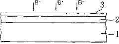
图1是现有技术的薄膜晶体管的剖视图,该薄膜晶体管具有所谓的顶栅结构,即栅电极形成于薄半导体层之上。FIG. 1 is a cross-sectional view of a prior art thin film transistor having a so-called top-gate structure, that is, a gate electrode is formed on a thin semiconductor layer.
如图1所述,薄膜晶体管包括:绝缘基板101,例如玻璃基板;绝缘膜102,形成在基板101上;薄半导体层103,由多晶硅膜构成,形成在绝缘膜102上,并且具有在薄半导体层103大致中央形成的沟道区104,以及在沟道区104周围形成的源区和漏区105、106;栅绝缘膜107,形成在沟道区104之上;栅电极108形成在栅绝缘膜107之上;层间绝缘膜109,由氧化硅膜构成,形成于基板101的整个表面上;以及源电极和漏电极111、112,在接触孔110中形成,接触孔110贯通层间绝缘膜109而形成,以使源区105和漏区106通过接触孔110而露出来。As shown in FIG. 1, a thin film transistor includes: an insulating substrate 101, such as a glass substrate; an insulating film 102 formed on the substrate 101; a thin semiconductor layer 103 formed of a polysilicon film formed on the insulating film 102, and having A channel region 104 formed approximately in the center of the layer 103, and source and drain regions 105, 106 formed around the channel region 104; a gate insulating film 107 formed on the channel region 104; a gate electrode 108 formed on the gate insulating film film 107; an interlayer insulating film 109, made of a silicon oxide film, formed on the entire surface of the substrate 101; and source and drain electrodes 111, 112 formed in a contact hole 110 penetrating through the interlayer insulating The film 109 is formed so that the source region 105 and the drain region 106 are exposed through the contact hole 110 .
栅电极108由耐熔金属,例如铬(Cr)、钼(Mo)或钨(W)构成。源电极111和漏电极112包含由铝或以铝为主要成份的铝合金构成的导电膜,因为铝和铝合金是与通过腐蚀而形成小的几何形状,并且具有较小电阻。The gate electrode 108 is made of a refractory metal such as chromium (Cr), molybdenum (Mo) or tungsten (W). The source electrode 111 and the drain electrode 112 contain a conductive film composed of aluminum or an aluminum alloy mainly composed of aluminum because aluminum and aluminum alloys are formed into small geometric shapes by corrosion and have small electrical resistance.
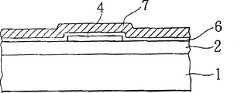
图2是另一个现有技术中的薄膜晶体管的剖视图,该薄膜晶体管具有所谓的底栅结构,即栅电极形成在薄半导体层之下。FIG. 2 is a cross-sectional view of another prior art thin film transistor having a so-called bottom-gate structure, that is, a gate electrode is formed under a thin semiconductor layer.
图2所示的薄膜晶体管与图1所示的薄膜晶体管相比,仅栅电极108的位置不同。图2所示的薄膜晶体管与图1所示的薄膜晶体管具有相同的原理。The thin film transistor shown in FIG. 2 differs from the thin film transistor shown in FIG. 1 only in the position of the gate electrode 108 . The thin film transistor shown in FIG. 2 has the same principle as the thin film transistor shown in FIG. 1 .
为了制造图1和图2的现有技术的薄膜晶体管,采用了各种工艺,例如用于把栅极金属膜如铬膜构图为栅电极108的等离子腐蚀,用于激活薄半导体层103的激光退火,用于形成接触孔110对层间绝缘膜109的等离子腐蚀。In order to manufacture the prior art thin film transistors of FIGS. 1 and 2, various processes are used, such as plasma etching for patterning a gate metal film such as a chromium film into the gate electrode 108, laser light for activating the thin semiconductor layer 103, etc. Annealing, plasma etching of the interlayer insulating film 109 for forming the contact hole 110 .
这些工艺产生以下问题,即由于层103和107被等离子引起的静电损伤,使薄半导体层103、栅绝缘膜107和/或薄半导体层103和栅绝缘膜107之间的界面产生结晶缺陷。上述结晶缺陷会产以下问题,即薄膜晶体管的特性例如阈值电压的离散,引起薄膜晶体管可靠性的恶化。因此,要求提供解决结晶缺陷问题的办法。These processes pose a problem of generating crystal defects in thin semiconductor layer 103, gate insulating film 107, and/or the interface between thin semiconductor layer 103 and gate insulating film 107 due to electrostatic damage of layers 103 and 107 by plasma. The above-mentioned crystal defects cause the problem that the characteristics of the thin film transistor such as the dispersion of the threshold voltage cause the deterioration of the reliability of the thin film transistor. Therefore, it is required to provide a solution to the problem of crystal defects.
在日本专利申请公报No.2000-252472A中公开了一种制造如下所述的薄膜晶体管的方法。A method of manufacturing a thin film transistor as described below is disclosed in Japanese Patent Application Publication No. 2000-252472A.
该方法包括以下步骤:在绝缘基板上形成包括多晶硅层的薄半导体层的步骤;将硼或磷等杂质离子注入多晶硅层的一部分中,用于在多晶硅层上形成源区和漏区;通过等离子增强化学气相淀积(CVD)在基板上形成氧化硅膜等层间绝缘膜;在600℃条件下对基板热退火1小时,用于激活多晶硅膜以及减少在栅绝缘膜和栅绝缘膜与多晶硅膜之间的界面上的结晶缺陷。The method includes the steps of: forming a thin semiconductor layer including a polysilicon layer on an insulating substrate; implanting impurity ions such as boron or phosphorus into a part of the polysilicon layer for forming a source region and a drain region on the polysilicon layer; Enhanced chemical vapor deposition (CVD) to form interlayer insulating films such as silicon oxide films on the substrate; thermal annealing of the substrate at 600°C for 1 hour is used to activate the polysilicon film and reduce the gap between the gate insulating film and the gate insulating film and polysilicon. Crystalline defects at the interface between films.
在日本专利申请公报No.10-154815A中公开了以下另一种制造上述薄膜晶体管的方法。Another method of manufacturing the above thin film transistor is disclosed in Japanese Patent Application Publication No. 10-154815A as follows.
该方法包括以下步骤:在绝缘基板上形成由非晶硅膜构成的薄半导体层;在基板上形成栅绝缘膜;在非晶硅膜之上的栅绝缘膜上形成栅电级;将杂质离子注入非晶硅层的一部分,以在非晶硅层中形成源区和漏区;形成由Cr、Mo、Ta和W之一构成的层;在200~400℃下进行数小时的热退火,以使Cr、Mo、Ta或W扩散到源区和漏区中,在源区和漏区表面形成薄硅化物层。The method comprises the steps of: forming a thin semiconductor layer composed of an amorphous silicon film on an insulating substrate; forming a gate insulating film on the substrate; forming a gate electrode on the gate insulating film above the amorphous silicon film; Implanting a part of the amorphous silicon layer to form source and drain regions in the amorphous silicon layer; forming a layer composed of one of Cr, Mo, Ta, and W; performing thermal annealing at 200-400°C for several hours, Diffusion of Cr, Mo, Ta or W into the source region and the drain region to form a thin silicide layer on the surface of the source region and the drain region.
但是,上述现有技术的方法伴随有以下问题,即当源电极和漏电极包括有铝或以铝为主要成份的铝合金构成的导电膜时,将不能阻止结晶缺陷,导致薄膜晶体管特性的离散。However, the method of the prior art described above is accompanied by the problem that when the source electrode and the drain electrode include a conductive film composed of aluminum or an aluminum alloy mainly composed of aluminum, crystal defects cannot be prevented, resulting in dispersion of thin film transistor characteristics. .
特别是当栅电极由现有技术的薄膜晶体管制造方法而形成时,采用了很多工艺,例如用于对铬膜等栅极膜进行构图的等离子腐蚀,用于激活薄半导体层的激光退火,用于形成接触孔对层间绝缘膜的等离子腐蚀。Especially when the gate electrode is formed by the prior art thin film transistor manufacturing method, many processes such as plasma etching for patterning a gate film such as a chrome film, laser annealing for activating a thin semiconductor layer, and Plasma etching of the interlayer insulating film for forming contact holes.
这些工艺产生以下问题,即由于薄半导体层和栅绝缘膜被等离子引起的静电损伤,使得在薄半导体层、栅绝缘膜和/或薄半导体层和栅绝缘膜之间的界面上产生结晶缺陷。这导致薄膜晶体管特性例如阈值电压的离散。These processes pose a problem that crystal defects are generated on the thin semiconductor layer, the gate insulating film and/or the interface between the thin semiconductor layer and the gate insulating film due to electrostatic damage of the thin semiconductor layer and the gate insulating film by plasma. This leads to dispersion of thin film transistor characteristics such as threshold voltage.
在薄膜晶体管制造方法的第1现有技术中,在600℃下对基板进行1小时的热退火,然后形成源电极和漏电极。然而即使像这样在源电极和漏电极形成前进行热退火,在源电极和漏电极形成时也会发生结晶缺陷。因此,即使形成源电极和漏电极之前进行上述热处理也不能改善结晶缺陷。In the first prior art of a thin film transistor manufacturing method, a substrate is thermally annealed at 600° C. for 1 hour, and then a source electrode and a drain electrode are formed. However, even if thermal annealing is performed before the formation of the source electrode and the drain electrode, crystal defects will occur when the source electrode and the drain electrode are formed. Therefore, even if the above heat treatment is performed before the formation of the source electrode and the drain electrode, crystal defects cannot be improved.
在制造薄膜晶体管的方法的第2现有技术中,在形成源区和漏区之后但在形成源电极和漏电极之前,在200~400℃下对基板进行数小时的热退火。与第1现有技术相同,第2现有技术也伴随有以下问题,即在形成源电极和漏电极时也会发生结晶缺陷。其结果是第2现有技术也不能改善结晶缺陷。In the second prior art of the method of manufacturing a thin film transistor, the substrate is thermally annealed at 200 to 400° C. for several hours after forming the source and drain regions but before forming the source and drain electrodes. Like the first prior art, the second prior art also suffers from the problem that crystal defects occur even when the source electrode and the drain electrode are formed. As a result, crystal defects cannot be improved even in the second prior art.
日本专利申请公开No.8-125022A公开了以下半导体器件的制造方法,该方法具有以下步骤:在半导体基板的某一区域上形成耐熔金属硅化物膜;在耐熔金属硅化物膜上形成硅膜;形成将硅膜和基板某一区域电连接的电极;在形成于基板上的绝缘膜上形成多晶硅膜;将多晶硅膜构图成为器件;在形成多晶硅之后在氧化气氛中,按预定时刻对基板进行热退火。Japanese Patent Application Laid-Open No. 8-125022A discloses a method of manufacturing a semiconductor device having the steps of: forming a refractory metal silicide film on a certain region of a semiconductor substrate; film; form an electrode that electrically connects the silicon film to a certain area of the substrate; form a polysilicon film on the insulating film formed on the substrate; pattern the polysilicon film into a device; Perform thermal annealing.
日本专利申请公开No.10-22507A公开了以下薄膜晶体管阵列的制造方法,该方法包括以下步骤:在绝缘透明基板上形成由铝构成的第1金属膜;在第1金属膜上形成以铝为主要成份的铝合金构成的第2金属膜;通过对第2金属膜进行局部阳极氧化而形成阳极氧化膜,以保留作为栅电极和源电极的第1和第2金属膜的一部分不被去除。Japanese Patent Application Laid-Open No. 10-22507A discloses a manufacturing method of the following thin film transistor array, the method comprising the following steps: forming a first metal film made of aluminum on an insulating transparent substrate; forming a metal film made of aluminum on the first metal film The second metal film composed of aluminum alloy as the main component; the anodized film is formed by partially anodizing the second metal film, so as to keep a part of the first and second metal films serving as gate electrodes and source electrodes from being removed.
日本专利申请公开No.2001-28445A公开了以下半导体器件的制造方法,该方法包括以下步骤:在绝缘膜上形成薄膜晶体管;在薄膜晶体管之上形成绝缘膜;对基板进行热退火。Japanese Patent Application Laid-Open No. 2001-28445A discloses a method of manufacturing a semiconductor device including the steps of: forming a thin film transistor on an insulating film; forming an insulating film over the thin film transistor; and thermally annealing a substrate.
发明内容Contents of the invention
鉴于现有技术中的上述问题,本发明之目的在于,提供一种薄膜晶体管的制造方法,该方法能阻止包括其源电极和漏电极分别由导电膜组成的薄膜晶体管特性的变化,上述导电膜由铝或以铝为主要成份的铝合金构成。In view of the above-mentioned problems in the prior art, the purpose of the present invention is to provide a method for manufacturing a thin film transistor, which can prevent changes in the characteristics of a thin film transistor including its source electrode and drain electrode respectively composed of conductive films. Composed of aluminum or an aluminum alloy with aluminum as the main component.
本发明提供一种薄膜晶体管的制造方法,该薄膜晶体管包括:绝缘基板、在上述基板上形成的半导体层和在形成于上述半导体层中的源区和漏区之上的形成的源电极和漏电极,上述源电极和漏电极由铝或铝合金构成,上述方法包括以下步骤:(a)通过栅绝缘膜形成与上述半导体层电绝缘的栅电极;(b)将具有预定导电率的杂质的离子注入到用于形成上述源区和漏区的上述半导体层的至少一部分中;(c)在上述基板的整个表面上形成层间绝缘膜;(d)形成贯通上述层间绝缘膜的接触孔,使得上述源区和漏区的至少一部分通过上述接触孔而露出来;(e)在上述接触孔中形成由铝或铝合金构成的导电膜,以使上述源电极和漏电极通过上述接触孔与上述源区和漏区电连接;以及(f)在275~350℃条件下,在惰性气氛中对基板进行1.5~3小时的热退火。The invention provides a method for manufacturing a thin film transistor, which includes: an insulating substrate, a semiconductor layer formed on the substrate, and a source electrode and a drain electrode formed on the source region and the drain region formed in the semiconductor layer. The above-mentioned source electrode and drain electrode are made of aluminum or an aluminum alloy, and the above-mentioned method includes the following steps: (a) forming a gate electrode electrically insulated from the above-mentioned semiconductor layer through a gate insulating film; ion implantation into at least a part of the above-mentioned semiconductor layer for forming the above-mentioned source region and drain region; (c) forming an interlayer insulating film on the entire surface of the above-mentioned substrate; (d) forming a contact hole penetrating the above-mentioned interlayer insulating film , so that at least a part of the above-mentioned source region and drain region is exposed through the above-mentioned contact hole; (e) forming a conductive film made of aluminum or aluminum alloy in the above-mentioned contact hole, so that the above-mentioned source electrode and drain electrode pass through the above-mentioned contact hole It is electrically connected to the source region and the drain region; and (f) performing thermal annealing on the substrate in an inert atmosphere at 275-350° C. for 1.5-3 hours.
以下对本发明的优点进行说明。Advantages of the present invention will be described below.
根据本发明,在形成由铝或以铝为主要成份的铝合金构成的源电极和漏电极之后,在275~350℃条件下,对基板进行1.5~3小时的热退火。这样可以改善结晶缺陷,因此,即使在晶体管具有由铝或以铝为主要成份的铝合金构成的源电极和漏电极的情况下,也能阻止薄膜晶体管特性的离散。According to the present invention, after forming the source electrode and drain electrode made of aluminum or aluminum alloy with aluminum as the main component, the substrate is subjected to thermal annealing at 275-350° C. for 1.5-3 hours. This can improve crystal defects, and therefore prevent dispersion of thin film transistor characteristics even in the case of a transistor having source and drain electrodes composed of aluminum or an aluminum alloy having aluminum as a main component.
附图说明Description of drawings
图1是现有技术的薄膜晶体管的剖视图;1 is a cross-sectional view of a thin film transistor of the prior art;
图2是另一个现有技术的薄膜晶体管的剖视图;2 is a cross-sectional view of another prior art thin film transistor;
图3A~3K是根据本发明第一实施例的薄膜晶体管制造方法的各个步骤中的薄膜晶体管剖视图;3A to 3K are cross-sectional views of thin film transistors in various steps of the thin film transistor manufacturing method according to the first embodiment of the present invention;
图4是表示在第一实施例所涉及的方法中采用的退火的温度曲线图;Fig. 4 is a graph showing the temperature profile of annealing used in the method related to the first embodiment;
图5A和图5B是根据本发明第二实施例的薄膜晶体管制造方法的各个步骤中的薄膜晶体管剖视图;5A and 5B are cross-sectional views of thin film transistors in various steps of a thin film transistor manufacturing method according to a second embodiment of the present invention;
图6A至图6I是根据本发明第三实施例的薄膜晶体管制造方法的各个步骤中的薄膜晶体管剖视图;6A to 6I are cross-sectional views of thin film transistors in various steps of the thin film transistor manufacturing method according to the third embodiment of the present invention;
具体实施方式Detailed ways
[第一实施例][first embodiment]
图3A至图3K是根据第一实施例的薄膜晶体管制造方法的各步骤中的薄膜晶体管剖视图。图4是表示这种方法中进行热退火时的温度曲线,以下根据第一实施例解释薄膜晶体管的制造方法。3A to 3K are cross-sectional views of a thin film transistor in each step of the method of manufacturing the thin film transistor according to the first embodiment. FIG. 4 is a graph showing a temperature profile when thermal annealing is performed in this method, and a method of manufacturing a thin film transistor will be explained below based on a first embodiment.
在第一实施例中制造具有顶栅结构的N沟型薄膜晶体管。An N-channel type thin film transistor having a top gate structure is fabricated in the first embodiment.
首先,如图3A所示,用化学气相淀积(CVD)方法在电绝缘基板上形成基底膜2。该基板由厚度为约0.7mm的玻璃基板构成。该基底膜2由厚度为约300nm的氧化硅膜构成。该基底膜2用作缓冲膜,防止那些对薄膜晶体管特性有不良影响的杂质从基板1进入到后述的薄膜半导体层中。First, as shown in FIG. 3A, a
如图3B所示,在整个基底膜2上用CVD方法形成厚度为约60nm的非晶硅膜3。As shown in FIG. 3B, an amorphous silicon film 3 having a thickness of about 60 nm is formed on the
将P型杂质如硼的离子注入到整个非晶硅膜3中,以便激活将构成薄膜晶体管沟道区的非晶硅膜3。应注意不一定进行这种对非晶硅膜3的离子注入。Ions of a P-type impurity such as boron are implanted into the entire amorphous silicon film 3 so as to activate the amorphous silicon film 3 which will constitute a channel region of the thin film transistor. It should be noted that such ion implantation into the amorphous silicon film 3 is not necessarily performed.
接下来如图3C所示,对整个非晶硅膜3照射由准分子激光器产生的能量束,以使非晶硅膜3转变为多晶硅膜4。同时,利用这种能量束使被注入了硼离子的多晶硅膜4退火,从而激活。Next, as shown in FIG. 3C , the entire amorphous silicon film 3 is irradiated with an energy beam generated by an excimer laser to convert the amorphous silicon film 3 into a
在基板1上形成厚度为约60nm的多晶硅膜4,作为薄半导体层,将基底膜2加在其中。A
接下来,如图3D所示,用光刻技术和等离子腐蚀将多晶硅膜4构图为岛状,将多晶硅膜4不必要的部分用等离子腐蚀有选择地去掉,只留下用于制造薄膜晶体管所需的多晶硅膜4部分。在这种等离子腐蚀中,岛状的多晶硅膜4被等离子引起的静电损伤,导致可能在多晶硅膜4中引起结晶缺陷。Next, as shown in FIG. 3D, the
如图3E所示,通过CVD在整个多晶硅膜4和基底膜2上形成绝缘膜6,绝缘膜6由氧化硅构成,其厚度为约50nm。As shown in FIG. 3E, insulating
如图3F所示,通过溅射法在绝缘膜6上形成栅金属膜7。该栅金属膜7由铬构成,其厚度为约200nm。As shown in FIG. 3F, gate metal film 7 is formed on insulating
如图3G所示,利用光刻技术和等离子腐蚀去掉绝缘膜6和栅极金属膜7的不需要部分,因而形成具有所希望图形的栅绝缘膜8和栅电极9。在等离子腐蚀过程中,多晶硅膜4、栅绝缘膜8以及多晶硅膜4和栅绝缘膜8之间的界面会被等离子引起的静电损伤,结果可能会在这些部位引起结晶缺陷。As shown in FIG. 3G, unnecessary portions of insulating
如图3H所示,把栅电极9作为掩模,用自对准方式把N型杂质离子如磷(P)注入到多晶硅膜4的一部分中。因而在栅电极9周围的多晶硅膜4中形成N型源区10和漏区11,进而在位于栅电极9下方的区域形成沟道区12,该沟道区被夹在源区10和漏区11之间。As shown in FIG. 3H, using the
接着,通过激光退火,将注入了磷离子的多晶硅膜4激活。然后,对多晶硅膜4施加氢等离子,使载流子容易通过沟道区12。Next,
当通过将N型杂质离子注入到多晶硅膜4而形成N型源区10和漏区11时,源区10和漏区11可被设计成通过以不同浓度分两次离子注入而具有轻掺杂漏区(LDD)结构。特别是,当薄膜晶体管被设置成具有十分小的沟道长度时,这种LDD结构对增强薄膜晶体管的工作可靠性十分有效,因为LDD结构能够防止电场集中到漏区。When the N-
如图3I所示,通过CVD法在基板1全表面上形成层间绝缘膜13。层间绝缘膜13是由氧化硅构成的,其厚度为约300nm。As shown in FIG. 3I, an
接下来,如图3J所示,通过光刻技术和等离子腐蚀去掉层间绝缘膜13的不必要部分,因而形成贯通层间绝缘膜13的接触孔14。通过接触孔14部分露出源区10和漏区11。在等离子腐蚀过程中,多晶硅薄4、栅绝缘膜8以及多晶硅膜4和栅绝缘膜8之间的界面会受到等离子引起的静电损伤,结果可能会在这些层中引起结晶缺陷。Next, as shown in FIG. 3J , unnecessary portions of the
接下来参考图3K,通过溅射法在图3J所示的所得基板全表面上形成铝膜,用铝膜填充接触孔14。然后,通过光刻技术和等离子腐蚀去掉铝膜的不必要部分,把铝膜构图成所希望的图形。于是,形成通过接触孔14分别与源区10和漏区11电连接的源电极15和漏电极16。然后形成布线层(未图示)。在等离子腐蚀过程中,多晶硅薄4、栅绝缘膜8以及多晶硅膜4和栅绝缘膜8之间的界面会受到等离子引起的静电损伤,结果可能会在这些层中引起结晶缺陷。Referring next to FIG. 3K, an aluminum film is formed on the entire surface of the resulting substrate shown in FIG. 3J by sputtering, and the
在形成上述由铝膜构成的源电极15与漏电极16之后立即把基板1放置到加热炉内,按如图4所示的温度曲线在氮(N2)气氛中进行热处理。Immediately after forming the above-mentioned
具体地讲,由图4可知,在炉子内的温度在时刻t0~t1约30分钟期间内由室温升温到300℃后,在时刻t1~t2约2小时内保持约300℃,接下来在时刻t2~t3约3小时内由约300℃降到室温。通过在t1~t2约2小时将炉子保持在约300℃,使基板1被热退火。使得在等离子腐蚀过程中,多晶硅薄4、栅绝缘膜8以及多晶硅膜4和栅绝缘膜8之间的界面受到静电引起的结晶缺陷减少。Specifically, it can be seen from Fig. 4 that after the temperature in the furnace is raised from room temperature to 300°C within about 30 minutes from time t0 to t1, it is kept at about 300°C within about 2 hours from time t1 to t2, and then at time From about 300°C to room temperature within about 3 hours from t2 to t3. The
接下来,形成与源电极15或漏电极16电连接的像素电极(未图示)。然后在所得基板全表面上形成平坦化膜和钝化膜(未图示)。完成薄膜晶体管。Next, a pixel electrode (not shown) electrically connected to the
在上述方法中,根据第一实施例,在形成源电极15和漏电极16之后立即在约300℃氮气氛中对基板1热退火2小时。因此,即使进行了诸如用于把栅极金属膜7构图成栅电极9的等离子腐蚀、用于激活多晶硅膜4的激光退火以及用于形成贯通层间绝缘膜13的接触孔4的等离子腐蚀,也可以减少在多晶硅薄4、栅绝缘膜8以及多晶硅膜4和栅绝缘膜8之间的界面上,在这些过程中引起的结晶缺陷。另外作为减少结晶缺陷的结果,也可能控制载流子在结晶缺陷中的散射。In the above method, according to the first embodiment, the
结果,能减小薄膜晶体管的阈值离散。具体地,约减小40%离散。例如,0.1V的离散可减小到0.06V。进而,上述热处理减少了由铝膜构成的源电极15和漏电极16的接触电阻。As a result, threshold variation of the thin film transistor can be reduced. Specifically, about a 40% reduction in dispersion. For example, a dispersion of 0.1V can be reduced to 0.06V. Furthermore, the heat treatment described above reduces the contact resistance of the
在将上述薄膜晶体管作为驱动器的液晶显示装置中,源电极15和漏电极16分别被定义为栅极线和数据线。一般液晶显示装置被设计成包括用来防止液晶显示装置受等离子引起的静电的保护器。在源电极15和漏电极16形成之后进行的各步骤中,由于保护器工作即该保护器保护多晶硅膜4、栅绝缘膜8等等免遭等离子引起的静电。In the liquid crystal display device using the above thin film transistor as a driver, the
在源电极15和漏电极16形成之后,立即用上述方式对基板1进行热退火可以有效地减少结晶缺陷。其结果减小了薄膜晶体管的特性离散,能够提高薄膜晶体管的可靠性。Immediately after the formation of the
[第二实施例][Second embodiment]
图5A和5B是根据第二实施例的薄膜晶体管的制造方法的主要步骤中的薄膜晶体管剖视图。5A and 5B are cross-sectional views of the thin film transistor in main steps of the method of manufacturing the thin film transistor according to the second embodiment.
除非特别说明,与第一实施例相对应的那些部件和元件标以相同的标号,并以与第一实施例中相对应的部件和元件相同的方式工作。Those parts and elements corresponding to those of the first embodiment are designated with the same reference numerals and operate in the same manner as the corresponding parts and elements of the first embodiment, unless otherwise specified.
第二实施例与第一实施例不同点在于,层间绝缘膜被设计成具有多层结构。The second embodiment differs from the first embodiment in that the interlayer insulating film is designed to have a multilayer structure.
具体地说,如图5A所示,在参照图3K解释的步骤之后,通过CVD在基板1的全表面上形成第二层间绝缘膜17。第二层间绝缘膜17由氮化硅构成,其厚度为约400nm。第二层间绝缘膜17和层间绝缘膜13限定多层的层间绝缘膜。Specifically, as shown in FIG. 5A, after the step explained with reference to FIG. 3K, a second
接着,如图5B所示,通过光刻技术和等离子腐蚀去掉第二层间绝缘膜17的不必要部分,从而形成接触孔18,部分地露出源电极15和漏电极16。在等离子腐蚀过程中,多晶硅薄4、栅绝缘膜8以及多晶硅膜4和栅绝缘膜8之间的界面会受到等离子引起的静电损伤。结果可能会在这些层中引起结晶缺陷。Next, as shown in FIG. 5B, unnecessary portions of the second
通过溅射法在所得基板全表面上形成铝膜,以便用铝填充接触孔18,然后,通过用光刻和等离子腐蚀去掉铝膜的不必要部分,将铝膜构图成所需要的图形。形成通过接触孔分别与源电极15和漏电极16电连接的源电极19和漏电极20,并且形成布线层(未图示)。在等离子腐蚀过程中,多晶硅薄4、栅绝缘膜8以及多晶硅膜4和栅绝缘膜8之间的界面会受到等离子引起的静电损伤,结果可能会在这些层中引起结晶缺陷。An aluminum film is formed on the entire surface of the resulting substrate by sputtering to fill the
在源电极15、19和漏电极16、20形成之后,立即把基板1放入炉中,然后与第一实施例相同,按图4所示的温度曲线在氮气氛中进行热退火。Immediately after the
具体地讲,在t1~t2期间,将炉子保持在300℃约2小时,对基板1进行热退火,结果使得在等离子腐蚀过程中,多晶硅薄4、栅绝缘膜8以及多晶硅膜4和栅绝缘膜8之间的界面受到静电引起的结晶缺陷减少。Specifically, during the period from t1 to t2, the furnace is kept at 300°C for about 2 hours, and the
形成与源电极19或漏电极20电连接的像素电极(未图示)。然后在所得基板全表面上形成平坦化膜和钝化膜(未图示)。完成薄膜晶体管。A pixel electrode (not shown) electrically connected to the
由于除了层间绝缘薄具有包括层间绝缘膜13和17的多层结构之外,第二实施例与第一实施例相同,第二实施例提供了由第一实施例所提供的那些优点。Since the second embodiment is the same as the first embodiment except that the interlayer insulating film has a multilayer structure including the
[第三实施例][Third embodiment]
图6A至图6I是根据第三实施方式的薄膜晶体管制造方法的各个步骤中的薄膜晶体管剖视图。以下参照图6A至图6I解释根据第三实施例的薄膜晶体管的制造方法。6A to 6I are cross-sectional views of a thin film transistor in respective steps of a method of manufacturing a thin film transistor according to a third embodiment. A method of manufacturing a thin film transistor according to the third embodiment is explained below with reference to FIGS. 6A to 6I .
第三实施例在以下方面与第一实施例不同,即第三实施例应用于具有底栅结构的薄膜晶体管,而第一实施例应用于具有顶栅结构的薄膜晶体管。The third embodiment differs from the first embodiment in that the third embodiment is applied to a thin film transistor having a bottom gate structure whereas the first embodiment is applied to a thin film transistor having a top gate structure.
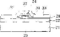
首先,如图6A所示,通过CVD在绝缘基板21上形成基底膜22。基板21由具有约0.7mm厚度的玻璃基板构成。基底膜22由具有约400nm厚度的氧化硅膜组成。以基底膜22作为缓冲膜,以阻止对薄膜晶体管有不良影响的杂质从绝缘基板21侵入到后述的薄半导体层。First, as shown in FIG. 6A ,
然后,利用溅射法在基板21的整个表面上形成栅极金属膜。栅极金属膜由铬构成,具有约200nm的厚度。Then, a gate metal film is formed on the entire surface of the
然后,通过光刻或等离子腐蚀去除栅极金属膜的不必要部分,从而形成具有所要求形状的栅电极29。Then, unnecessary portions of the gate metal film are removed by photolithography or plasma etching, thereby forming
然后,如图6B所示,通过CVD法在基板21的整个表面上形成栅绝缘膜28。栅绝缘膜由氧化硅构成,具有约60nm的厚度。Then, as shown in FIG. 6B, a
然后,通过CVD法在基板21的整个表面上形成厚度约60nm的非晶硅膜23。Then, an
然后,如图6C所示,向整个非晶硅膜23注入P型杂质如硼(B)的离子,以激活将成为薄膜晶体管的沟道区的非晶硅膜23。应注意,并不总是需要将离子注入到非晶硅膜23中。Then, as shown in FIG. 6C, ions of a P-type impurity such as boron (B) are implanted into the entire
然后,如图6D所示,从准分子激光器向非晶硅膜的整个表面照射能量束,以将非晶硅膜23转变为多晶硅膜24。同时,通过能量束对被注入了硼离子的多晶硅膜24进行退火,使其激活。Then, as shown in FIG. 6D , an energy beam is irradiated from an excimer laser to the entire surface of the amorphous silicon film to convert the
然后,如图6E所示,然后通过光刻和等离子腐蚀,把多晶硅膜构图为岛区,以通过等离子腐蚀有选择地去除多晶硅膜24不必要部分,保留用于制造薄膜晶体管的多晶硅膜24的需要部分不被腐蚀。在该等离子腐蚀中,岛形多晶硅膜24被等离子引起的静电损伤,从而可能导致在多晶硅膜24中产生结晶缺陷。Then, as shown in FIG. 6E, the polysilicon film is patterned into island regions by photolithography and plasma etching, so as to selectively remove unnecessary parts of the
然后,在整个基板21上形成抗蚀剂膜,并将其构图成为覆盖栅电极29的掩模5。Then, a resist film is formed on the
然后,如图6F所示,将抗蚀剂膜5作为掩模,将N型杂质例如磷(P)的离子注入多晶硅膜14的一部分,从而在栅电极29周围的多晶硅膜24中形成N型源区30和漏区31,进而在位于栅电极29之上的区域中形成沟道区32,该沟道区32被夹在源区30和漏区31之间。Then, as shown in FIG. 6F, using the resist
然后,通过激光退火使被注入了磷离子的多晶硅膜24激活,对多晶硅膜24施加氢等离子,从而使载流子容易通过沟道区32。Then, the
当通过向多晶硅膜24中注入N型杂质离子而形成N型源区30和漏区31时,与第一实施例相同,通过以不同杂质浓度分两次进行离子注入,源区30和漏区31可以被设计为具有轻掺杂漏区(LDD)结构。When the N-
然后,如图6G所示,通过CVD法在基板21整个表面上形成层间绝缘膜33。层间绝缘膜由氧化硅构成,具有约300nm的厚度。Then, as shown in FIG. 6G, an
然后,如图6H所示,通过光刻和等离子腐蚀去除层间绝缘膜33的不必要部分,从而形成贯通层间绝缘膜33的接触孔34。源区和漏区30、31从接触孔34部分被露出。在等离子腐蚀过程中,多晶硅膜24、栅绝缘膜28、以及多晶硅膜24与栅绝缘膜28之间的界面被由等离子引起的静电损伤,可能会导致在上述膜中引起结晶缺陷。Then, as shown in FIG. 6H , unnecessary portions of the
然后,如图6I所示,通过溅射法基板21的整个表面上形成铝膜,以便用铝膜填充接触孔34。然后,通过借助于光刻和等离子腐蚀去除铝膜的不必要部分,从而把铝膜构图为所要求的图形,这样,分别形成了通过接触孔34与源区和漏区30、31电连接的源电极35和漏电极36,进而形成布线层(未图示)。在等离子腐蚀过程中,多晶硅膜24、栅绝缘膜28、以及多晶硅膜24与栅绝缘膜28之间的界面被由等离子引起的静电损伤,可能会在上述膜中引起结晶缺陷。Then, as shown in FIG. 6I, an aluminum film is formed on the entire surface of the
在形成源电极和漏电极35、36之后,将基板21放入炉中,然后在氮气气氛中按照图4所示的温度曲线进行热退火。After the source and drain electrodes 35, 36 are formed, the
具体地讲,使炉子保持300℃左右的温度,在t1到t2时刻之间的约2小时之内对基板21进行退火,其结果是,多晶硅膜24、栅绝缘膜28、以及多晶硅膜24与栅绝缘膜28之间的界面在等离子腐蚀中由静电引起的结晶缺陷被减少。Specifically, the furnace is kept at a temperature of about 300° C., and the
然后,形成与源电极35或漏电极36电连接的像素电极(未图示)。然后,在上述所得基板的整个表面上形成平坦化膜和钝化膜(未图示)。这样就完成了薄膜晶体管。Then, a pixel electrode (not shown) electrically connected to the source electrode 35 or the drain electrode 36 is formed. Then, a planarization film and a passivation film (not shown) are formed on the entire surface of the above-obtained substrate. This completes the thin film transistor.
除了栅电极29具有底栅结构之外,第三实施例与第一实施例相同,所以第三实施例可以获得与第一实施例相同的效果。The third embodiment is the same as the first embodiment except that the
例如,在第一实施例和第二实施例中,在氮气氛中、约300℃温度下对基板1和21进行约2小时的热退火。根据发明人进行的实验,发现基本可以在氮气氛、275~350℃温度下被热退火约1.5~3小时。For example, in the first embodiment and the second embodiment, the
在第一和第二实施例中,基板1和21在氮气氛中被热退火。根据发明人进行的实验,发现基板可以在除了氮气氛之外的惰性气氛中被热退火。例如,基板可以在氩(Ar)、氖(Ne)或氦(He)气氛中被热退火。In the first and second embodiments, the
此外,第三实施例中的具有底栅结构的薄膜晶体管可以被设计为具有多层层间绝缘膜,像第二实施例那样。Furthermore, the thin film transistor having the bottom gate structure in the third embodiment can be designed to have a multilayer interlayer insulating film like the second embodiment.
在第一和第二实施例中,源电极和漏电极由铝构成。作为变型例,它们可以被设计为由以铝为主要成份的铝合金构成。In the first and second embodiments, the source electrode and the drain electrode are made of aluminum. As a variant, they can be designed to consist of an aluminum alloy whose main component is aluminum.
作为注入薄半导体层以形成N型源区和漏区的杂质,可以选择锑(Sb)来代替磷(P)。作为变型例,可以形成P型源区和漏区,来代替N型源区和漏区,在该情况下,向薄半导体层注入P型杂质例如硼的离子。As impurities implanted into the thin semiconductor layer to form N-type source and drain regions, antimony (Sb) may be selected instead of phosphorus (P). As a modification, P-type source and drain regions may be formed instead of N-type source and drain regions, in which case P-type impurities such as boron ions are implanted into the thin semiconductor layer.
绝缘基板、基底膜、薄半导体层、栅绝缘膜、栅电极和层间绝缘膜的厚度仅仅是示例,可以变为适当的厚度。The thicknesses of the insulating substrate, base film, thin semiconductor layer, gate insulating film, gate electrode, and interlayer insulating film are merely examples, and may be changed to appropriate thicknesses.
Claims (10)
Applications Claiming Priority (2)
| Application Number | Priority Date | Filing Date | Title |
|---|---|---|---|
| JP2002237048AJP2004079735A (en) | 2002-08-15 | 2002-08-15 | Method for manufacturing thin film transistor |
| JP237048/2002 | 2002-08-15 |
Publications (2)
| Publication Number | Publication Date |
|---|---|
| CN1487569Atrue CN1487569A (en) | 2004-04-07 |
| CN1329966C CN1329966C (en) | 2007-08-01 |
Family
ID=31712066
Family Applications (1)
| Application Number | Title | Priority Date | Filing Date |
|---|---|---|---|
| CNB031543278AExpired - Fee RelatedCN1329966C (en) | 2002-08-15 | 2003-08-15 | Method for producing thin film transistor |
Country Status (4)
| Country | Link |
|---|---|
| US (1) | US7071040B2 (en) |
| JP (1) | JP2004079735A (en) |
| KR (1) | KR100588174B1 (en) |
| CN (1) | CN1329966C (en) |
Cited By (1)
| Publication number | Priority date | Publication date | Assignee | Title |
|---|---|---|---|---|
| US8058654B2 (en) | 2008-02-29 | 2011-11-15 | Hitachi Displays, Ltd. | Display device and manufacturing method thereof |
Families Citing this family (13)
| Publication number | Priority date | Publication date | Assignee | Title |
|---|---|---|---|---|
| US7208401B2 (en)* | 2004-03-12 | 2007-04-24 | Hewlett-Packard Development Company, L.P. | Method for forming a thin film |
| KR101050903B1 (en)* | 2004-04-29 | 2011-07-20 | 엘지디스플레이 주식회사 | Polycrystalline Silicon Thin Film Transistor and Manufacturing Method Thereof |
| US7432141B2 (en)* | 2004-09-08 | 2008-10-07 | Sandisk 3D Llc | Large-grain p-doped polysilicon films for use in thin film transistors |
| KR101383705B1 (en) | 2007-12-18 | 2014-04-10 | 삼성디스플레이 주식회사 | Thin film transistor, display device and method for manufacturing the same |
| KR101002665B1 (en)* | 2008-07-02 | 2010-12-21 | 삼성모바일디스플레이주식회사 | Thin film transistor, manufacturing method thereof and organic light emitting display device comprising same |
| KR101015388B1 (en)* | 2008-12-31 | 2011-02-17 | 재단법인 광양만권 유아이티연구소 | Wired / wireless sensor data transmission device |
| KR101600879B1 (en)* | 2010-03-16 | 2016-03-09 | 삼성디스플레이 주식회사 | Thin film transistor, manufacturing method thereof and display substrate using the thin film transistor |
| US9111795B2 (en)* | 2011-04-29 | 2015-08-18 | Semiconductor Energy Laboratory Co., Ltd. | Semiconductor device with capacitor connected to memory element through oxide semiconductor film |
| CN102306634A (en)* | 2011-09-06 | 2012-01-04 | 深圳市华星光电技术有限公司 | Thin film transistor substrate and manufacturing method thereof |
| TWI518916B (en) | 2013-03-25 | 2016-01-21 | 友達光電股份有限公司 | Manufacturing method and structure of pixel structure |
| KR101447998B1 (en)* | 2013-11-22 | 2014-10-14 | 삼성디스플레이 주식회사 | Method for manufacturing display device |
| KR20170087574A (en)* | 2016-01-20 | 2017-07-31 | 삼성디스플레이 주식회사 | Liquid crystal display device and manufacturing method thereof |
| US10672490B2 (en)* | 2018-01-17 | 2020-06-02 | International Business Machines Corporation | One-time-programmable memory in a high-density three-dimensional structure |
Family Cites Families (15)
| Publication number | Priority date | Publication date | Assignee | Title |
|---|---|---|---|---|
| JPS6461062A (en)* | 1987-09-01 | 1989-03-08 | Ricoh Kk | Manufacture of thin film transistor |
| JP2660451B2 (en)* | 1990-11-19 | 1997-10-08 | 三菱電機株式会社 | Semiconductor device and manufacturing method thereof |
| JP3352998B2 (en) | 1991-08-26 | 2002-12-03 | 株式会社半導体エネルギー研究所 | Method for manufacturing semiconductor device |
| JP3494304B2 (en)* | 1993-02-01 | 2004-02-09 | 富士ゼロックス株式会社 | Method for manufacturing thin film semiconductor device |
| JP3565911B2 (en)* | 1994-08-11 | 2004-09-15 | 株式会社半導体エネルギー研究所 | Method for manufacturing semiconductor device |
| JP2699891B2 (en) | 1994-10-28 | 1998-01-19 | 日本電気株式会社 | Method for manufacturing semiconductor device |
| JP2978746B2 (en)* | 1995-10-31 | 1999-11-15 | 日本電気株式会社 | Method for manufacturing semiconductor device |
| DE69727033T2 (en)* | 1996-06-06 | 2004-11-11 | Seiko Epson Corp. | METHOD FOR PRODUCING A THIN-LAYER FIELD EFFECT TRANSISTOR, LIQUID CRYSTAL DISPLAY AND ELECTRONIC ARRANGEMENT PRODUCED BY IT |
| JPH1022507A (en) | 1996-07-02 | 1998-01-23 | Matsushita Electric Ind Co Ltd | Thin film transistor array and method of manufacturing the same |
| JP3587004B2 (en)* | 1996-11-05 | 2004-11-10 | ソニー株式会社 | Capacitor structure of semiconductor memory cell and method of manufacturing the same |
| JPH10154815A (en) | 1996-11-25 | 1998-06-09 | Furontetsuku:Kk | Thin film transistor, method of manufacturing the same, and liquid crystal display device using the same |
| US5801100A (en)* | 1997-03-07 | 1998-09-01 | Industrial Technology Research Institute | Electroless copper plating method for forming integrated circuit structures |
| TW468269B (en)* | 1999-01-28 | 2001-12-11 | Semiconductor Energy Lab | Serial-to-parallel conversion circuit, and semiconductor display device employing the same |
| JP2000252472A (en) | 1999-03-02 | 2000-09-14 | Matsushita Electric Ind Co Ltd | Thin film semiconductor device and method of manufacturing the same |
| JP2002026030A (en)* | 2000-07-05 | 2002-01-25 | Sony Corp | Semiconductor device and method of manufacturing the same |
- 2002
- 2002-08-15JPJP2002237048Apatent/JP2004079735A/enactivePending
- 2003
- 2003-08-13USUS10/639,478patent/US7071040B2/ennot_activeExpired - Lifetime
- 2003-08-14KRKR1020030056368Apatent/KR100588174B1/ennot_activeExpired - Fee Related
- 2003-08-15CNCNB031543278Apatent/CN1329966C/ennot_activeExpired - Fee Related
Cited By (2)
| Publication number | Priority date | Publication date | Assignee | Title |
|---|---|---|---|---|
| US8058654B2 (en) | 2008-02-29 | 2011-11-15 | Hitachi Displays, Ltd. | Display device and manufacturing method thereof |
| CN101521210B (en)* | 2008-02-29 | 2012-05-23 | 株式会社日立显示器 | Display device and manufacturing method thereof |
Also Published As
| Publication number | Publication date |
|---|---|
| US7071040B2 (en) | 2006-07-04 |
| JP2004079735A (en) | 2004-03-11 |
| CN1329966C (en) | 2007-08-01 |
| KR100588174B1 (en) | 2006-06-08 |
| US20040033648A1 (en) | 2004-02-19 |
| KR20040016411A (en) | 2004-02-21 |
Similar Documents
| Publication | Publication Date | Title |
|---|---|---|
| CN1173388C (en) | Semiconductor device having thin film transistor | |
| CN1249818C (en) | Semiconductor device and manufacturing method thereof | |
| CN1187802C (en) | Method for manufacturing thin film transistor containing crystallization silicon active layer | |
| CN1156016C (en) | Metal-insulator-semiconductor type semiconductor device and method of manufacturing the same | |
| CN1078386C (en) | Method for manufacturing semiconductor device | |
| JP5059703B2 (en) | THIN FILM TRANSISTOR, ITS MANUFACTURING METHOD, ORGANIC ELECTROLUMINESCENT DISPLAY DEVICE INCLUDING THE SAME, AND ITS MANUFACTURING METHOD | |
| CN1120240A (en) | Semiconductor device and manufacturing method thereof | |
| TWI518916B (en) | Manufacturing method and structure of pixel structure | |
| CN1652347A (en) | Semiconductor device and method of forming the same | |
| CN103839825A (en) | Low-temperature polycrystalline silicon thin film transistor, array substrate and manufacturing method of array substrate | |
| JPWO2002095834A1 (en) | Thin film transistor, active matrix display device, and manufacturing method thereof | |
| CN1487569A (en) | Method for producing thin film transistor | |
| CN1051640C (en) | Semiconductor device and method for fabricating the same | |
| JP2010145984A (en) | Organic electroluminescent display device and method of manufacturing the same | |
| CN1691340A (en) | Electronic device and method of manufacturing same | |
| JP2008252108A (en) | Semiconductor device | |
| CN1501437A (en) | Mask for polycrystallization and method of manufacturing thin film transistor using same | |
| CN1402357A (en) | Field effect transistor and mfg. method thereof, and liquid crystal display device and mfg. method thereof | |
| CN1121741C (en) | Semiconductor device and manufacturing method thereof | |
| CN1702879A (en) | Thin film transistor substrate and fabrication method thereof | |
| CN1725510A (en) | Low temperature polysilicon thin film transistor and its manufacturing method | |
| KR101457705B1 (en) | Fabricating method of electric device | |
| CN2717021Y (en) | Low Temperature Polysilicon Thin Film Transistor | |
| CN1892996A (en) | Method for manufacturing thin film transistor and method for repairing defects in polysilicon film layer | |
| CN1133489A (en) | Method for making semiconductor device |
Legal Events
| Date | Code | Title | Description |
|---|---|---|---|
| C06 | Publication | ||
| PB01 | Publication | ||
| C10 | Entry into substantive examination | ||
| SE01 | Entry into force of request for substantive examination | ||
| C14 | Grant of patent or utility model | ||
| GR01 | Patent grant | ||
| ASS | Succession or assignment of patent right | Owner name:GETENA FUND CO., LTD. Free format text:FORMER OWNER: NEC CORP. Effective date:20110810 | |
| C41 | Transfer of patent application or patent right or utility model | ||
| TR01 | Transfer of patent right | Effective date of registration:20110810 Address after:Delaware, USA Patentee after:Nippon Electric Co. Address before:Tokyo, Japan Patentee before:NEC Corp. | |
| C17 | Cessation of patent right | ||
| CF01 | Termination of patent right due to non-payment of annual fee | Granted publication date:20070801 Termination date:20130815 |