CN1485891A - Semiconductor memory device and method for manufacturing semiconductor device - Google Patents
Semiconductor memory device and method for manufacturing semiconductor deviceDownload PDFInfo
- Publication number
- CN1485891A CN1485891ACNA031560822ACN03156082ACN1485891ACN 1485891 ACN1485891 ACN 1485891ACN A031560822 ACNA031560822 ACN A031560822ACN 03156082 ACN03156082 ACN 03156082ACN 1485891 ACN1485891 ACN 1485891A
- Authority
- CN
- China
- Prior art keywords
- film
- silicon dioxide
- silicon nitride
- semiconductor device
- silicon
- Prior art date
- Legal status (The legal status is an assumption and is not a legal conclusion. Google has not performed a legal analysis and makes no representation as to the accuracy of the status listed.)
- Pending
Links
Images


Classifications
- H—ELECTRICITY
- H10—SEMICONDUCTOR DEVICES; ELECTRIC SOLID-STATE DEVICES NOT OTHERWISE PROVIDED FOR
- H10B—ELECTRONIC MEMORY DEVICES
- H10B69/00—Erasable-and-programmable ROM [EPROM] devices not provided for in groups H10B41/00 - H10B63/00, e.g. ultraviolet erasable-and-programmable ROM [UVEPROM] devices
- H—ELECTRICITY
- H01—ELECTRIC ELEMENTS
- H01L—SEMICONDUCTOR DEVICES NOT COVERED BY CLASS H10
- H01L21/00—Processes or apparatus adapted for the manufacture or treatment of semiconductor or solid state devices or of parts thereof
- H01L21/02—Manufacture or treatment of semiconductor devices or of parts thereof
- H01L21/02104—Forming layers
- H01L21/02107—Forming insulating materials on a substrate
- H01L21/02296—Forming insulating materials on a substrate characterised by the treatment performed before or after the formation of the layer
- H01L21/02318—Forming insulating materials on a substrate characterised by the treatment performed before or after the formation of the layer post-treatment
- H01L21/02337—Forming insulating materials on a substrate characterised by the treatment performed before or after the formation of the layer post-treatment treatment by exposure to a gas or vapour
- H01L21/0234—Forming insulating materials on a substrate characterised by the treatment performed before or after the formation of the layer post-treatment treatment by exposure to a gas or vapour treatment by exposure to a plasma
- H—ELECTRICITY
- H01—ELECTRIC ELEMENTS
- H01L—SEMICONDUCTOR DEVICES NOT COVERED BY CLASS H10
- H01L21/00—Processes or apparatus adapted for the manufacture or treatment of semiconductor or solid state devices or of parts thereof
- H01L21/02—Manufacture or treatment of semiconductor devices or of parts thereof
- H01L21/02104—Forming layers
- H01L21/02107—Forming insulating materials on a substrate
- H01L21/02109—Forming insulating materials on a substrate characterised by the type of layer, e.g. type of material, porous/non-porous, pre-cursors, mixtures or laminates
- H01L21/02112—Forming insulating materials on a substrate characterised by the type of layer, e.g. type of material, porous/non-porous, pre-cursors, mixtures or laminates characterised by the material of the layer
- H01L21/02123—Forming insulating materials on a substrate characterised by the type of layer, e.g. type of material, porous/non-porous, pre-cursors, mixtures or laminates characterised by the material of the layer the material containing silicon
- H01L21/02164—Forming insulating materials on a substrate characterised by the type of layer, e.g. type of material, porous/non-porous, pre-cursors, mixtures or laminates characterised by the material of the layer the material containing silicon the material being a silicon oxide, e.g. SiO2
- H—ELECTRICITY
- H01—ELECTRIC ELEMENTS
- H01L—SEMICONDUCTOR DEVICES NOT COVERED BY CLASS H10
- H01L21/00—Processes or apparatus adapted for the manufacture or treatment of semiconductor or solid state devices or of parts thereof
- H01L21/02—Manufacture or treatment of semiconductor devices or of parts thereof
- H01L21/02104—Forming layers
- H01L21/02107—Forming insulating materials on a substrate
- H01L21/02296—Forming insulating materials on a substrate characterised by the treatment performed before or after the formation of the layer
- H01L21/02318—Forming insulating materials on a substrate characterised by the treatment performed before or after the formation of the layer post-treatment
- H01L21/02321—Forming insulating materials on a substrate characterised by the treatment performed before or after the formation of the layer post-treatment introduction of substances into an already existing insulating layer
- H01L21/02323—Forming insulating materials on a substrate characterised by the treatment performed before or after the formation of the layer post-treatment introduction of substances into an already existing insulating layer introduction of oxygen
- H01L21/02326—Forming insulating materials on a substrate characterised by the treatment performed before or after the formation of the layer post-treatment introduction of substances into an already existing insulating layer introduction of oxygen into a nitride layer, e.g. changing SiN to SiON
- H—ELECTRICITY
- H01—ELECTRIC ELEMENTS
- H01L—SEMICONDUCTOR DEVICES NOT COVERED BY CLASS H10
- H01L21/00—Processes or apparatus adapted for the manufacture or treatment of semiconductor or solid state devices or of parts thereof
- H01L21/02—Manufacture or treatment of semiconductor devices or of parts thereof
- H01L21/02104—Forming layers
- H01L21/02107—Forming insulating materials on a substrate
- H01L21/02296—Forming insulating materials on a substrate characterised by the treatment performed before or after the formation of the layer
- H01L21/02318—Forming insulating materials on a substrate characterised by the treatment performed before or after the formation of the layer post-treatment
- H01L21/02321—Forming insulating materials on a substrate characterised by the treatment performed before or after the formation of the layer post-treatment introduction of substances into an already existing insulating layer
- H01L21/02329—Forming insulating materials on a substrate characterised by the treatment performed before or after the formation of the layer post-treatment introduction of substances into an already existing insulating layer introduction of nitrogen
- H01L21/02332—Forming insulating materials on a substrate characterised by the treatment performed before or after the formation of the layer post-treatment introduction of substances into an already existing insulating layer introduction of nitrogen into an oxide layer, e.g. changing SiO to SiON
- H—ELECTRICITY
- H10—SEMICONDUCTOR DEVICES; ELECTRIC SOLID-STATE DEVICES NOT OTHERWISE PROVIDED FOR
- H10B—ELECTRONIC MEMORY DEVICES
- H10B41/00—Electrically erasable-and-programmable ROM [EEPROM] devices comprising floating gates
- H10B41/40—Electrically erasable-and-programmable ROM [EEPROM] devices comprising floating gates characterised by the peripheral circuit region
- H10B41/42—Simultaneous manufacture of periphery and memory cells
- H10B41/49—Simultaneous manufacture of periphery and memory cells comprising different types of peripheral transistor
- H—ELECTRICITY
- H10—SEMICONDUCTOR DEVICES; ELECTRIC SOLID-STATE DEVICES NOT OTHERWISE PROVIDED FOR
- H10B—ELECTRONIC MEMORY DEVICES
- H10B43/00—EEPROM devices comprising charge-trapping gate insulators
- H10B43/30—EEPROM devices comprising charge-trapping gate insulators characterised by the memory core region
- H—ELECTRICITY
- H01—ELECTRIC ELEMENTS
- H01L—SEMICONDUCTOR DEVICES NOT COVERED BY CLASS H10
- H01L21/00—Processes or apparatus adapted for the manufacture or treatment of semiconductor or solid state devices or of parts thereof
- H01L21/02—Manufacture or treatment of semiconductor devices or of parts thereof
- H01L21/02104—Forming layers
- H01L21/02107—Forming insulating materials on a substrate
- H01L21/02109—Forming insulating materials on a substrate characterised by the type of layer, e.g. type of material, porous/non-porous, pre-cursors, mixtures or laminates
- H01L21/02112—Forming insulating materials on a substrate characterised by the type of layer, e.g. type of material, porous/non-porous, pre-cursors, mixtures or laminates characterised by the material of the layer
- H01L21/02123—Forming insulating materials on a substrate characterised by the type of layer, e.g. type of material, porous/non-porous, pre-cursors, mixtures or laminates characterised by the material of the layer the material containing silicon
- H01L21/02126—Forming insulating materials on a substrate characterised by the type of layer, e.g. type of material, porous/non-porous, pre-cursors, mixtures or laminates characterised by the material of the layer the material containing silicon the material containing Si, O, and at least one of H, N, C, F, or other non-metal elements, e.g. SiOC, SiOC:H or SiONC
- H01L21/0214—Forming insulating materials on a substrate characterised by the type of layer, e.g. type of material, porous/non-porous, pre-cursors, mixtures or laminates characterised by the material of the layer the material containing silicon the material containing Si, O, and at least one of H, N, C, F, or other non-metal elements, e.g. SiOC, SiOC:H or SiONC the material being a silicon oxynitride, e.g. SiON or SiON:H
- H—ELECTRICITY
- H01—ELECTRIC ELEMENTS
- H01L—SEMICONDUCTOR DEVICES NOT COVERED BY CLASS H10
- H01L21/00—Processes or apparatus adapted for the manufacture or treatment of semiconductor or solid state devices or of parts thereof
- H01L21/02—Manufacture or treatment of semiconductor devices or of parts thereof
- H01L21/02104—Forming layers
- H01L21/02107—Forming insulating materials on a substrate
- H01L21/02109—Forming insulating materials on a substrate characterised by the type of layer, e.g. type of material, porous/non-porous, pre-cursors, mixtures or laminates
- H01L21/02112—Forming insulating materials on a substrate characterised by the type of layer, e.g. type of material, porous/non-porous, pre-cursors, mixtures or laminates characterised by the material of the layer
- H01L21/02123—Forming insulating materials on a substrate characterised by the type of layer, e.g. type of material, porous/non-porous, pre-cursors, mixtures or laminates characterised by the material of the layer the material containing silicon
- H01L21/0217—Forming insulating materials on a substrate characterised by the type of layer, e.g. type of material, porous/non-porous, pre-cursors, mixtures or laminates characterised by the material of the layer the material containing silicon the material being a silicon nitride not containing oxygen, e.g. SixNy or SixByNz
- H—ELECTRICITY
- H01—ELECTRIC ELEMENTS
- H01L—SEMICONDUCTOR DEVICES NOT COVERED BY CLASS H10
- H01L21/00—Processes or apparatus adapted for the manufacture or treatment of semiconductor or solid state devices or of parts thereof
- H01L21/02—Manufacture or treatment of semiconductor devices or of parts thereof
- H01L21/02104—Forming layers
- H01L21/02107—Forming insulating materials on a substrate
- H01L21/02109—Forming insulating materials on a substrate characterised by the type of layer, e.g. type of material, porous/non-porous, pre-cursors, mixtures or laminates
- H01L21/022—Forming insulating materials on a substrate characterised by the type of layer, e.g. type of material, porous/non-porous, pre-cursors, mixtures or laminates the layer being a laminate, i.e. composed of sublayers, e.g. stacks of alternating high-k metal oxides
- Y—GENERAL TAGGING OF NEW TECHNOLOGICAL DEVELOPMENTS; GENERAL TAGGING OF CROSS-SECTIONAL TECHNOLOGIES SPANNING OVER SEVERAL SECTIONS OF THE IPC; TECHNICAL SUBJECTS COVERED BY FORMER USPC CROSS-REFERENCE ART COLLECTIONS [XRACs] AND DIGESTS
- Y10—TECHNICAL SUBJECTS COVERED BY FORMER USPC
- Y10S—TECHNICAL SUBJECTS COVERED BY FORMER USPC CROSS-REFERENCE ART COLLECTIONS [XRACs] AND DIGESTS
- Y10S438/00—Semiconductor device manufacturing: process
- Y10S438/954—Making oxide-nitride-oxide device
Landscapes
- Engineering & Computer Science (AREA)
- Manufacturing & Machinery (AREA)
- Physics & Mathematics (AREA)
- Condensed Matter Physics & Semiconductors (AREA)
- General Physics & Mathematics (AREA)
- Computer Hardware Design (AREA)
- Microelectronics & Electronic Packaging (AREA)
- Power Engineering (AREA)
- Plasma & Fusion (AREA)
- Non-Volatile Memory (AREA)
- Semiconductor Memories (AREA)
- Formation Of Insulating Films (AREA)
Abstract
Translated fromChinese
Description
Translated fromChinese本申请基于并且要求2002年8月30日向日本专利局提出的日本专利申请No.2002-256195的优先权,在此全文引入作为参考。This application is based on and claims the benefit of priority from Japanese Patent Application No. 2002-256195 filed with the Japan Patent Office on August 30, 2002, which is hereby incorporated by reference in its entirety.
技术领域technical field
本发明涉及一种制造具有栅绝缘膜或者包含氮化膜的介电膜的半导体器件的方法,以及能够通过在氮化膜中存储电荷而保持信息的半导体存储器件。The present invention relates to a method of manufacturing a semiconductor device having a gate insulating film or a dielectric film including a nitride film, and a semiconductor memory device capable of retaining information by storing charges in the nitride film.
背景技术Background technique
近来,将由二氧化硅膜上形成的氮化硅膜构成的ON膜,以及由二氧化硅膜、氮化硅膜和二氧化硅膜按顺序构成的ONO膜用作半导体存储器件的存储单元。Recently, an ON film composed of a silicon nitride film formed on a silicon dioxide film, and an ONO film composed of a silicon dioxide film, a silicon nitride film and a silicon dioxide film in this order are used as a memory cell of a semiconductor memory device.
在对于各个存储单元具有作为电荷存储部分的岛形浮栅的浮栅型非易失性半导体存储器(下文中简称为浮栅型存储器)中,将诸如ON膜、ONO膜等等的多层绝缘膜(下文中简称为多层绝缘膜)用作具有高介电常数和低泄漏电流的电容绝缘膜。在具有氮化硅膜作为电荷存储部分的SONOS型或者MNOS型的非易失性半导体存储器(下文中简称为SONOS型(MNOS型)存储器)中,将多层绝缘膜用作电荷存储部分的栅绝缘膜。In a floating gate type nonvolatile semiconductor memory having an island-shaped floating gate as a charge storage portion for each memory cell (hereinafter simply referred to as a floating gate type memory), a multi-layer insulating layer such as an ON film, an ONO film, etc. film (hereinafter simply referred to as a multilayer insulating film) functions as a capacitive insulating film having a high dielectric constant and low leakage current. In a SONOS type or MNOS type nonvolatile semiconductor memory having a silicon nitride film as a charge storage portion (hereinafter simply referred to as a SONOS type (MNOS type) memory), a multilayer insulating film is used as a gate of the charge storage portion. insulating film.
最近,对半导体存储器的小型化和高性能要求的趋势进一步加强,从而出现了下面的与形成多层绝缘膜有关的严重问题。Recently, the trend toward miniaturization and high performance requirements for semiconductor memories has further intensified, so that the following serious problems related to the formation of multilayer insulating films have arisen.
—生成氢的影响——Effect of hydrogen generation—
位于SONOS型存储器、MNOS型存储器等等中的ONO膜和ON膜的底层上的下层二氧化硅膜作为隧道氧化膜(tunnel oxide film),并且需要很高的可靠性。因此,通常,在干氧化中,在1000℃或者更高的温度条件下,而在湿氧化中,在800℃或者更高的温度条件下,通过对硅表面的热氧化而形成下层二氧化硅膜。The lower silicon dioxide film on the bottom layer of the ONO film and the ON film in the SONOS type memory, the MNOS type memory, etc. serves as a tunnel oxide film, and requires high reliability. Therefore, generally, under the temperature condition of 1000°C or higher in dry oxidation and 800°C or higher in wet oxidation, the underlying silicon dioxide is formed by thermal oxidation of the silicon surface. membrane.
然后,在下层二氧化硅膜上形成用作电荷存储部分的氮化硅膜。使用氨气和硅烷作为原料气、通过热CVD方法而进行沉积。除了需要较高的均匀性外,基于下面的原因,还将温度条件设定为700℃至900℃。Then, a silicon nitride film serving as a charge storage portion is formed on the underlying silicon dioxide film. Deposition was performed by a thermal CVD method using ammonia gas and silane as raw material gases. In addition to the need for higher uniformity, the temperature condition is set to 700°C to 900°C for the following reasons.
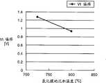
此处,对于SONOS型存储器,图36显示了使氮化硅膜置于高温下而导致的阈值(Vt)偏移与氮化硅膜的沉积温度之间关系的研究结果。此特征曲线表明氮化硅膜的沉积温度越高,Vt偏移量越小,从而产生较好的结果。这可能是由下列原因造成的。Here, for the SONOS type memory, FIG. 36 shows the results of a study of the relationship between the threshold (Vt) shift caused by exposing the silicon nitride film to high temperature and the deposition temperature of the silicon nitride film. This characteristic curve shows that the higher the deposition temperature of the silicon nitride film, the smaller the Vt shift, resulting in better results. This may be caused by the following reasons.
当形成氮化硅膜时,从原料气体中生成大量的氢,并且在沉积氮化硅膜的同时进入下层二氧化硅膜中。同时,在氮化硅膜中也夹杂着大量的氢。此处,当形成ONO膜作为多层绝缘膜时,通过对氮化硅膜的表面进行进一步的热氧化而形成上层二氧化硅膜。然而,由于需要高温和长时间的热处理,使得夹杂在氮化硅膜中的氢得以扩散,并且进入下层二氧化硅膜。显然,氢进入下层二氧化硅膜导致恶化了下层二氧化硅膜的膜质量。When the silicon nitride film is formed, a large amount of hydrogen is generated from the source gas, and enters into the underlying silicon dioxide film at the same time as the silicon nitride film is deposited. At the same time, a large amount of hydrogen is also mixed in the silicon nitride film. Here, when an ONO film is formed as a multilayer insulating film, an upper layer silicon dioxide film is formed by further thermally oxidizing the surface of the silicon nitride film. However, due to the heat treatment required at high temperature and for a long time, the hydrogen contained in the silicon nitride film diffuses and enters the underlying silicon dioxide film. Apparently, the entry of hydrogen into the underlying silicon dioxide film leads to deterioration of the film quality of the underlying silicon dioxide film.
当氮化硅膜的沉积温度较高时,夹杂在氮化硅膜中的氢的量会减少。另外,在后面的处理中,通过扩散而进入到下层二氧化硅膜中的氢量减少,这减小了Vt偏移量。因此,需要在尽可能高的温度下形成氮化硅膜,以通过控制氢的生成而提高下层二氧化硅膜的膜质量并获得良好的Vt偏移。When the deposition temperature of the silicon nitride film is high, the amount of hydrogen contained in the silicon nitride film decreases. In addition, in subsequent processes, the amount of hydrogen entering into the underlying silicon dioxide film by diffusion is reduced, which reduces the Vt shift amount. Therefore, it is necessary to form the silicon nitride film at as high a temperature as possible in order to improve the film quality of the underlying silicon dioxide film and obtain a good Vt shift by controlling the generation of hydrogen.
对于浮栅型存储器,也存在相同的情况。由于需要较高的温度以形成多层绝缘膜,所以氢气通过浮栅而到达下层二氧化硅膜,导致恶化了用作隧道氧化膜的下层二氧化硅膜的质量。The same holds true for floating gate type memories. Since a higher temperature is required to form a multilayer insulating film, hydrogen gas passes through the floating gate to reach the underlying silicon dioxide film, resulting in deterioration of the quality of the underlying silicon dioxide film used as a tunnel oxide film.
—在高温下进行处理的影响——Effect of processing at high temperature—
如上所述,当形成包含用作电荷存储膜或介电膜的氮化硅膜的多层绝缘膜时,需要高温的温度条件,从而如下所述,阻止了的单元的小型化。As described above, when forming a multilayer insulating film including a silicon nitride film serving as a charge storage film or a dielectric film, high temperature temperature conditions are required, thereby preventing miniaturization of cells as described below.
在具有多层绝缘膜的存储器中,例如,当通过LOCOS方法或者STI(浅沟槽隔离)方法形成单元隔离结构时,在衬底上注入杂质而形成阱之后,形成多层绝缘膜。然而,通过上述的高温处理,阱中的杂质发生热扩散,导致很难实现单元的小型化。In a memory having a multilayer insulating film, for example, when forming a cell isolation structure by a LOCOS method or an STI (Shallow Trench Isolation) method, after impurity is implanted on a substrate to form a well, a multilayer insulating film is formed. However, impurities in the well are thermally diffused by the above-mentioned high-temperature treatment, making it difficult to miniaturize the cell.
尤其是,在源极/漏极也用作内建位线的存储器中,当在形成多层绝缘膜之后形成源极/漏极,以避免由于高温处理而导致的杂质热扩散时,由于杂质的离子注入而在多层绝缘膜中形成缺陷,导致泄漏电流增加或者可靠性降低等问题。In particular, in a memory in which the source/drain is also used as a built-in bit line, when the source/drain is formed after forming a multilayer insulating film in order to avoid thermal diffusion of impurities due to high-temperature processing, due to impurities Defects are formed in the multilayer insulating film due to ion implantation, leading to problems such as increased leakage current or reduced reliability.
如上所述,即使通过热CVD方法或者热氧化方法形成ON膜、ONO膜等等的多层绝缘膜,以试图进一步获得半导体存储器的小型化和高性能,也需要高温下的处理,从而阻止了单元的小型化。这造成了很难实现高性能的半导体存储器的现状。As described above, even if a multilayer insulating film of an ON film, an ONO film, etc. is formed by a thermal CVD method or a thermal oxidation method in an attempt to further achieve miniaturization and high performance of a semiconductor memory, processing at a high temperature is required, thereby preventing Unit miniaturization. This creates a situation where it is difficult to realize a high-performance semiconductor memory.
发明内容Contents of the invention
本发明致力于解决上述问题。本发明的一个目的是提供一种制造高可靠性的半导体器件和半导体存储器件的方法,其在低温下高质量地形成诸如ON膜、ONO膜等等的多层绝缘膜。The present invention addresses the above-mentioned problems. An object of the present invention is to provide a method of manufacturing a highly reliable semiconductor device and a semiconductor memory device which forms a multilayer insulating film such as an ON film, an ONO film, etc. with high quality at low temperature.
在经过深思熟虑之后,本发明的发明人设计了本发明的如下方面。After careful consideration, the inventors of the present invention devised the following aspects of the present invention.
根据本发明的一种制造半导体器件的方法包括:形成下层二氧化硅膜的步骤;在下层二氧化硅膜上形成硅膜的步骤;以及通过等离子氮化方法在下层二氧化硅膜上形成氮化硅膜,对硅膜进行完全氮化的步骤,其中形成了至少包含下层二氧化硅膜和氮化硅膜的多层绝缘膜。A method of manufacturing a semiconductor device according to the present invention includes: a step of forming a lower silicon dioxide film; a step of forming a silicon film on the lower silicon dioxide film; and forming nitrogen on the lower silicon dioxide film by a plasma nitriding method a silicon film, a step of completely nitriding the silicon film, in which a multilayer insulating film including at least an underlying silicon dioxide film and a silicon nitride film is formed.
根据本发明的一种制造半导体器件的方法包括:通过等离子氮化方法形成氮化硅膜,对硅区域的表面进行氮化的步骤;通过等离子氧化方法同时对氮化硅膜的表面和硅区域与氮化硅膜的界面进行氧化,同时在所述表面上形成上层二氧化硅膜和在所述界面上形成下层二氧化硅膜的步骤,其中形成了由下层二氧化硅膜、氮化硅膜和上层二氧化硅膜构成的多层绝缘膜。A method for manufacturing a semiconductor device according to the present invention includes: forming a silicon nitride film by a plasma nitriding method, and nitriding the surface of the silicon region; Oxidizing the interface with the silicon nitride film while forming an upper silicon dioxide film on the surface and a lower silicon dioxide film on the interface, wherein the lower silicon dioxide film, silicon nitride A multilayer insulating film composed of a silicon dioxide film and an upper silicon dioxide film.
根据本发明的一种制造半导体器件的方法包括:形成下层二氧化硅膜的步骤;通过CVD方法在下层二氧化硅膜上形成氮化硅膜的步骤;通过等离子氧化方法对氮化硅膜的表面进行氧化的步骤,其中形成了由下层二氧化硅膜、氮化硅膜和上层二氧化硅膜构成的多层绝缘膜。A method of manufacturing a semiconductor device according to the present invention includes: a step of forming a lower silicon dioxide film; a step of forming a silicon nitride film on the lower silicon dioxide film by a CVD method; A step in which the surface is oxidized, in which a multilayer insulating film composed of a lower silicon dioxide film, a silicon nitride film and an upper silicon dioxide film is formed.
根据本发明的一种半导体存储器件包含存储单元,存储单元包括半导体衬底;在半导体衬底上形成的包含具有电荷俘获功能的氮化硅膜的绝缘膜;通过绝缘膜在半导体衬底上形成的栅极;以及在半导体衬底上形成的一对杂质扩散层,其中氮化硅膜是仅通过由微波激励实现的等离子氮化,或者包含等离子氮化的一系列处理而形成的均匀而致密的氮化硅膜。A semiconductor memory device according to the present invention includes a memory cell, the memory cell includes a semiconductor substrate; an insulating film comprising a silicon nitride film having a charge trapping function formed on the semiconductor substrate; and an insulating film formed on the semiconductor substrate through the insulating film The gate; and a pair of impurity diffusion layers formed on the semiconductor substrate, wherein the silicon nitride film is uniform and dense formed only by plasma nitriding realized by microwave excitation, or a series of treatments including plasma nitriding silicon nitride film.
根据本发明的一种半导体存储器件包括:半导体衬底;在半导体衬底上形成的栅绝缘膜;通过该绝缘膜而在半导体衬底上形成的具有电荷俘获功能的岛形浮栅;在浮栅上形成的介电膜;通过介电膜而在浮栅上形成的控制栅;在半导体衬底上形成的一对杂质扩散层,其中氮化硅膜是仅通过由微波激励实现的等离子氮化,或者包含等离子氮化的一系列处理而形成的均匀而致密的氮化硅膜。A semiconductor storage device according to the present invention comprises: a semiconductor substrate; a gate insulating film formed on the semiconductor substrate; an island-shaped floating gate with charge trapping function formed on the semiconductor substrate through the insulating film; A dielectric film formed on a gate; a control gate formed on a floating gate through a dielectric film; a pair of impurity diffusion layers formed on a semiconductor substrate, in which the silicon nitride film is realized only by plasma nitrogen excited by microwaves Nitride, or a series of treatments including plasma nitriding to form a uniform and dense silicon nitride film.
附图说明Description of drawings
图1A至图1C是用于解释本发明的第一个方面的示意截面图;1A to 1C are schematic sectional views for explaining a first aspect of the present invention;
图2A和图2B是用于解释本发明的第二个方面的示意截面图;2A and 2B are schematic sectional views for explaining a second aspect of the present invention;
图3A和图3B是用于解释本发明的第三个方面的示意截面图;3A and 3B are schematic sectional views for explaining a third aspect of the present invention;
图4A和图4B是示意截面图,按照工艺顺序显示了第一个实施例中制造包含内建位线型SONOS晶体管的半导体存储器件的方法;4A and FIG. 4B are schematic cross-sectional views showing a method for manufacturing a semiconductor memory device including a built-in bit line type SONOS transistor in the first embodiment in accordance with the process sequence;
图5A和图5B接着图4A和图4B,按照工艺顺序显示了在第一个实施例中之后,制造包含内建位线型SONOS晶体管的半导体存储器件的方法;5A and FIG. 5B are subsequent to FIG. 4A and FIG. 4B, showing a method of manufacturing a semiconductor memory device comprising a built-in bit line type SONOS transistor after the first embodiment in the order of processes;
图6A和图6B接着图5A和图5B,按照工艺顺序显示了在第一个实施例中制造包含内建位线型SONOS晶体管的半导体存储器件的方法;6A and 6B are subsequent to FIG. 5A and FIG. 5B, showing a method of manufacturing a semiconductor memory device including a built-in bit line type SONOS transistor in the first embodiment in the order of processes;
图7A和图7B接着图6A和图6B,按照工艺顺序显示了在第一个实施例中制造包含内建位线型SONOS晶体管的半导体存储器件的方法;7A and 7B are subsequent to FIG. 6A and FIG. 6B, showing a method of manufacturing a semiconductor memory device including a built-in bit line type SONOS transistor in the first embodiment in the order of processes;
图8A和图8B接着图7A和图7B,按照工艺顺序显示了在第一个实施例中制造包含内建位线型SONOS晶体管的半导体存储器件的方法;8A and 8B are subsequent to FIG. 7A and FIG. 7B, showing a method of manufacturing a semiconductor memory device including a built-in bit line type SONOS transistor in the first embodiment in the order of processes;
图9A和图9B接着图8A和图8B,按照工艺顺序显示了在第一个实施例中制造包含内建位线型SONOS晶体管的半导体存储器件的方法;9A and 9B are subsequent to FIG. 8A and FIG. 8B, showing a method of manufacturing a semiconductor memory device including a built-in bit line type SONOS transistor in the first embodiment in the order of processes;
图10A和图10B接着图9A和图9B,按照工艺顺序显示了在第一个实施例中制造包含内建位线型SONOS晶体管的半导体存储器件的方法;10A and FIG. 10B are subsequent to FIG. 9A and FIG. 9B, showing a method of manufacturing a semiconductor memory device including a built-in bit line type SONOS transistor in the first embodiment in the order of processes;
图11A和图11B接着图10A和图10B,按照工艺顺序显示了在第一个实施例中制造包含内建位线型SONOS晶体管的半导体存储器件的方法;11A and 11B are subsequent to FIG. 10A and FIG. 10B, showing a method of manufacturing a semiconductor memory device including a built-in bit line type SONOS transistor in the first embodiment in the order of processes;
图12A和图12B接着图11A和图11B,按照工艺顺序显示了在第一个实施例中制造包含内建位线型SONOS晶体管的半导体存储器件的方法;12A and 12B are subsequent to FIG. 11A and FIG. 11B, showing a method of manufacturing a semiconductor memory device including a built-in bit line type SONOS transistor in the first embodiment in the order of processes;
图13A和图13B接着图12A和图12B,按照工艺顺序显示了在第一个实施例中制造包含内建位线型SONOS晶体管的半导体存储器件的方法;13A and 13B are subsequent to FIG. 12A and FIG. 12B, showing a method of manufacturing a semiconductor memory device including a built-in bit line type SONOS transistor in the first embodiment in the order of processes;
图14显示了具有用于各个实施例的径向线隙缝天线的等离子体处理器的示意结构;Figure 14 shows a schematic structure of a plasma processor with a radial line slot antenna for various embodiments;
图15A和图15B是示意截面图,按照工艺顺序显示了在第二个实施例中制造包含浮栅型晶体管的半导体存储器件的方法;15A and 15B are schematic cross-sectional views showing a method of manufacturing a semiconductor memory device including floating gate transistors in the second embodiment in the order of processes;
图16A和图16B接着图15A和图15B,按照工艺顺序显示了在第二个实施例中制造包含浮栅型晶体管的半导体存储器件的方法;16A and 16B are subsequent to FIG. 15A and FIG. 15B, showing a method of manufacturing a semiconductor memory device including floating gate transistors in the second embodiment in the order of processes;
图17A和图17B接着图16A和图16B,按照工艺顺序显示了在第二个实施例中制造包含浮栅型晶体管的半导体存储器件的方法;17A and 17B are subsequent to FIG. 16A and FIG. 16B, showing a method of manufacturing a semiconductor memory device including floating gate transistors in the second embodiment in the order of processes;
图18A和图18B接着图17A和图17B,按照工艺顺序显示了在第二个实施例中制造包含浮栅型晶体管的半导体存储器件的方法;18A and 18B follow from FIG. 17A and FIG. 17B, showing a method of manufacturing a semiconductor memory device including floating gate transistors in the second embodiment in the order of processes;
图19A和图19B接着图18A和图168之后,按照工艺顺序显示了在第二个实施例中制造包含浮栅型晶体管的半导体存储器件的方法;19A and FIG. 19B follow from FIG. 18A and FIG. 168 and show a method of manufacturing a semiconductor memory device including floating gate transistors in the second embodiment in the order of processes;
图20接着图19A和图19B,按照工艺顺序显示了在第二个实施例中制造包含浮栅型晶体管的半导体存储器件的方法;FIG. 20 is a continuation of FIG. 19A and FIG. 19B, showing a method of manufacturing a semiconductor memory device including floating gate transistors in the second embodiment in the order of processes;
图21A和图21B接着图20,按照工艺顺序显示了在第二个实施例中制造包含浮栅型晶体管的半导体存储器件的方法;21A and 21B follow from FIG. 20 and show a method of manufacturing a semiconductor memory device including a floating gate transistor in the second embodiment in the order of processes;
图22A和图22B接着图21A和图21B,按照工艺顺序显示了在第二个实施例中制造包含浮栅型晶体管的半导体存储器件的方法;22A and 22B are subsequent to FIG. 21A and FIG. 21B, showing a method of manufacturing a semiconductor memory device including floating gate transistors in the second embodiment in the order of processes;
图23A和图23B接着图22A和图22B,按照工艺顺序显示了在第二个实施例中制造包含浮栅型晶体管的半导体存储器件的方法;23A and 23B follow from FIG. 22A and FIG. 22B, showing a method of manufacturing a semiconductor memory device including floating gate transistors in the second embodiment in the order of processes;
图24A和图24B接着图23A和图23B,按照工艺顺序显示了在第二个实施例中制造包含浮栅型晶体管的半导体存储器件的方法;24A and FIG. 24B are subsequent to FIG. 23A and FIG. 23B, showing a method of manufacturing a semiconductor memory device including floating gate transistors in the second embodiment in the order of processes;
图25A和图25B接着图24A和图24B,按照工艺顺序显示了在第二个实施例中制造包含浮栅型晶体管的半导体存储器件的方法;25A and 25B are subsequent to FIG. 24A and FIG. 24B, showing a method of manufacturing a semiconductor memory device including floating gate transistors in the second embodiment in the order of processes;
图26A和图26B接着图25A和图25B,按照工艺顺序显示了在第二个实施例中制造包含浮栅型晶体管的半导体存储器件的方法;26A and 26B are subsequent to FIG. 25A and FIG. 25B, showing a method of manufacturing a semiconductor memory device including floating gate transistors in the second embodiment in the order of processes;
图27A和图27B是示意截面图,按照工艺顺序显示了在第三个实施例中制造包含内建位线型SONOS晶体管的半导体存储器件的方法;27A and 27B are schematic cross-sectional views showing a method of manufacturing a semiconductor memory device including a built-in bit line type SONOS transistor in the third embodiment in the order of processes;
图28A和图28B接着图27A和图27B,按照工艺顺序显示了在第三个实施例中制造包含内建位线型SONOS晶体管的半导体存储器件的方法;28A and 28B follow from FIG. 27A and FIG. 27B, showing a method of manufacturing a semiconductor memory device including a built-in bit line type SONOS transistor in the third embodiment in the order of processes;
图29A和图29B接着图28A和图28B,按照工艺顺序显示了在第三个实施例中制造包含内建位线型SONOS晶体管的半导体存储器件的方法;29A and 29B follow from FIG. 28A and FIG. 28B, showing a method of manufacturing a semiconductor memory device including a built-in bit line type SONOS transistor in the third embodiment in the order of processes;
图30A和图30B接着图29A和图29B,按照工艺顺序显示了在第三个实施例中制造包含内建位线型SONOS晶体管的半导体存储器件的方法;30A and 30B follow from FIG. 29A and FIG. 29B, showing a method of manufacturing a semiconductor memory device including a built-in bit line type SONOS transistor in the third embodiment in the order of processes;
图31A和图31B接着图30A和图30B,按照工艺顺序显示了在第三个实施例中制造包含内建位线型SONOS晶体管的半导体存储器件的方法;31A and 31B follow from FIG. 30A and FIG. 30B, showing a method of manufacturing a semiconductor memory device including a built-in bit line type SONOS transistor in the third embodiment in the order of processes;
图32A和图32B接着图31A和图31B,按照工艺顺序显示了在第三个实施例中制造包含内建位线型SONOS晶体管的半导体存储器件的方法;32A and 32B follow from FIG. 31A and FIG. 31B, showing a method of manufacturing a semiconductor memory device including a built-in bit line type SONOS transistor in the third embodiment in the order of processes;
图33A和图33B接着图32A和图32B,按照工艺顺序显示了在第三个实施例中制造包含内建位线型SONOS晶体管的半导体存储器件的方法;33A and 33B follow from FIG. 32A and FIG. 32B, showing a method of manufacturing a semiconductor memory device including a built-in bit line type SONOS transistor in the third embodiment in the order of processes;
图34A和图34B接着图33A和图33B,按照工艺顺序显示了在第三个实施例中制造包含内建位线型SONOS晶体管的半导体存储器件的方法;34A and 34B are subsequent to FIG. 33A and FIG. 33B, showing a method of manufacturing a semiconductor memory device including a built-in bit line type SONOS transistor in the third embodiment in the order of processes;
图35A和图35B接着图34A和图34B,按照工艺顺序显示了在第三个实施例中制造包含内建位线型SONOS晶体管的半导体存储器件的方法;35A and 35B follow from FIG. 34A and FIG. 34B, showing a method of manufacturing a semiconductor memory device including a built-in bit line type SONOS transistor in the third embodiment in the order of processes;
图36是氮化硅膜的沉积温度与将氮化硅膜置于高温下而导致的阈值(Vt)偏移之间关系的研究结果的特征曲线。FIG. 36 is a characteristic graph of the results of a study of the relationship between the deposition temperature of the silicon nitride film and the threshold (Vt) shift caused by exposing the silicon nitride film to a high temperature.
具体实施方式Detailed ways
—本发明的基本结构—-Basic structure of the present invention-
首先,对本发明的基本结构进行解释。First, the basic structure of the present invention is explained.
根据本发明,在整个制造处理中需要在低温条件下加热处理几分钟,具体而言,除了诸如RTA等等的在一分钟之内进行快速升温和快速降温的处理外,在600C或者更低的温度下制造半导体存储器件。考虑到上述处理,当形成氮化硅膜时,采用了使用由激发等离子体形成的氮基的氮化处理(等离子氮化方法),而不是需要高温的CVD方法。更进一步,除了氮化硅膜以外,多层绝缘膜中的二氧化硅膜也是通过等离子氧化方法形成的。According to the present invention, heat treatment at low temperature for several minutes is required throughout the manufacturing process, specifically, at 600C or lower, except for rapid heating and rapid cooling within one minute such as RTA and the like. Semiconductor memory devices are fabricated at high temperatures. In consideration of the above-mentioned processing, when forming a silicon nitride film, nitriding treatment using a nitrogen base formed by excited plasma (plasma nitriding method) is employed instead of a CVD method requiring a high temperature. Furthermore, in addition to the silicon nitride film, the silicon dioxide film in the multilayer insulating film is also formed by the plasma oxidation method.
等离子氮化方法是一种进行氮化处理的方法,其中,在除He、Ne、Ar、Kr、Xe和Rn中的一种或者多种惰性气体之外还包含含有氮原子的源气体的气氛中由微波激发等离子体,例如,除惰性气体之外还包含从NH3气、N2和H2的混合气以及N2气中所选择的一种,或者是NH3气和N2气的混合气,或者NH3气,N2和H2的混合气,从而生成氮基(N*基或者NH*基)。根据本方法,可以在大约200℃至600℃之间的低温下,获得致密和高质量的等离子氮化膜。应当注意,Ar和Kr适用于含有源气体的惰性气体;当使用Kr时,可以获得最佳质量的等离子氮化膜。另外,当使用包含氢的气体时,氧化速度较高。The plasma nitriding method is a method of performing nitriding treatment in which, in addition to one or more inert gases of He, Ne, Ar, Kr, Xe, and Rn, an atmosphere containing a source gas containing nitrogen atoms In the plasma excited by microwaves, for example, in addition to the inert gas, italso contains one selected from NH3 gas, a mixed gas of N2 and
等离子氧化方法是进行氧化处理的方法,在除He、Ne、Ar、Kr、Xe和Rn中的一种或者多种惰性气体之外还包含含有氧原子的源气体的气氛中由微波激发等离子体,例如,除惰性气体之外还包含从O2气、O2和H2的混合气以及H2O气中所选择的一种,或者是O2和H2O的混合气,或者是O2、H2和H2O气的混合气,从而生成氧基(O*基或者OH*基)。根据本方法,可以在大约200℃至600℃的低温下,获得致密和高质量的等离子氧化膜。应当注意,Ar和Kr是适于含有源气体的惰性气体;当使用Kr时,可以获得最佳质量的等离子氧化膜。另外,当使用包含氢的气体时,氧化速度较高。The plasma oxidation method is a method of performing an oxidation treatment in which plasma is excited by microwaves in an atmosphere containing a source gas containing oxygen atoms in addition to one or more inert gases of He, Ne, Ar, Kr, Xe, and Rn , for example, in addition to the inert gas, it also contains one selected from O2 gas, a mixed gas of
然而,当采用等离子氮化方法和等离子氧化方法时会出现下面的问题。However, the following problems arise when the plasma nitriding method and the plasma oxidation method are employed.
通常,在制造半导体存储器时,在包含存储单元区域的整个表面上形成诸如ON膜、ONO膜等等的多层绝缘膜之后,去除外围电路中的多层绝缘膜,并且在外围电路区域中通过热氧化而形成栅绝缘膜。在此情况下,使用多层绝缘膜覆盖存储单元区域。与衬底表面的氧化速度相比,氮化硅膜的氧化速度大约为1/30或者更低。另外,氮化硅膜不会使O2通过,从而,仅稍微地增厚了多层绝缘膜中的上层二氧化硅膜。当形成作为栅绝缘膜的氮氧化膜时,也是相同的情况。因为氮化硅膜不会使N2O或者NO通过,所以对存储单元中的多层绝缘膜影响不大。Usually, when manufacturing a semiconductor memory, after forming a multilayer insulating film such as an ON film, an ONO film, etc. on the entire surface including a memory cell region, the multilayer insulating film in the peripheral circuit is removed, and the thermally oxidized to form a gate insulating film. In this case, the memory cell region is covered with a multilayer insulating film. The oxidation rate of the silicon nitride film is about 1/30 or less compared to the oxidation rate of the substrate surface. In addition, the silicon nitride film does not passO2 , and thus, only slightly thickens the upper silicon dioxide film in the multilayer insulating film. The same is true when forming an oxynitride film as a gate insulating film. Since the silicon nitride film does not pass N2 O or NO, it has little influence on the multilayer insulating film in the memory cell.
然而,当在外围电路区域中形成栅绝缘膜时,以及当使用上述的等离子氧化方法或者等离子氮化方法时,由于O*基或者OH*基极强的氧化能力,或者N*基或者NH*基极强的氮化能力,当形成作为栅绝缘膜的二氧化硅膜时,存储单元中的多层绝缘膜中的氮化硅膜被氧化,并且在形成作为栅绝缘膜的氮氧化硅膜时,多层绝缘膜中的二氧化硅膜被进一步氮化。例如,由多层绝缘膜中的氮化硅膜的氧化所形成的二氧化硅膜的生长速率大约是硅衬底的氧化所形成的二氧化硅膜的生长速率的0.8倍。因此,氮化硅膜被置换成了二氧化硅膜(或者二氧化硅膜被置换成了氮化硅膜)。However, when the gate insulating film is formed in the peripheral circuit region, and when the above-mentioned plasma oxidation method or plasma nitriding method is used, due to the extremely strong oxidizing ability of the O* group or the OH* group, either the N* group or the NH* group The strong nitriding ability of the base, when forming the silicon dioxide film as the gate insulating film, the silicon nitride film in the multilayer insulating film in the memory cell is oxidized, and the silicon nitride oxide film as the gate insulating film is formed , the silicon dioxide film in the multilayer insulating film is further nitrided. For example, the growth rate of a silicon dioxide film formed by oxidation of a silicon nitride film in a multilayer insulating film is about 0.8 times that of a silicon dioxide film formed by oxidation of a silicon substrate. Therefore, the silicon nitride film is replaced with a silicon dioxide film (or the silicon dioxide film is replaced with a silicon nitride film).
考虑到当使用等离子氮化方法或者等离子氧化方法在较低的温度下形成致密和高质量的多层绝缘膜时,能够通过等离子氮化方法成功地形成外围电路,尤其是其中的栅绝缘膜,而不会产生氢,也不会导致与多层绝缘膜有关的问题,所以,本发明的发明人设计了如下方面。Considering that when a dense and high-quality multilayer insulating film is formed at a relatively low temperature using a plasma nitridation method or a plasma oxidization method, peripheral circuits, especially a gate insulating film therein, can be successfully formed by a plasma nitridation method, Without generating hydrogen and causing problems related to multilayer insulating films, the inventors of the present invention devised the following aspects.
—第一个方面—— the first aspect —
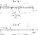
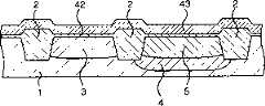
首先,对第一方面进行解释。图1A至图1C是用于解释第一个方面的示意图。其中,使用在存储单元区域中形成ONO膜并在外围电路区域中形成栅绝缘膜的实例进行解释。First, the first aspect is explained. 1A to 1C are schematic diagrams for explaining the first aspect. Herein, explanation is given using an example in which an ONO film is formed in a memory cell region and a gate insulating film is formed in a peripheral circuit region.
首先,在本实施例中,如图1A所示,当在作为硅半导体衬底的存储单元区域,或者作为存储单元区域中的多晶硅膜或者非晶硅(a-Si)膜(例如,岛形浮栅)的硅区域101上形成下层二氧化硅膜102之后,通过(例如)热CVD方法在下层二氧化硅膜102上形成硅膜103。可以将多晶硅膜或者a-Si膜作为硅膜103。a-Si膜可以在575℃或更低的温度下,例如低至530℃的温度下生长。通常使用包含氢原子的硅烷作为原料气体。然而,由于硅烷不包含氨,所以几乎不生成氢。然而,需要形成膜厚度为5nm或者更厚的硅膜103,以防止产生由沉积不均匀所导致的“缝隙”。First, in the present embodiment, as shown in FIG. 1A, when a memory cell region as a silicon semiconductor substrate, or a polysilicon film or an amorphous silicon (a-Si) film (for example, an island-shaped After the lower silicon dioxide film 102 is formed on the silicon region 101 of the floating gate), a silicon film 103 is formed on the lower silicon dioxide film 102 by, for example, a thermal CVD method. A polysilicon film or an a-Si film can be used as the silicon film 103 . The a-Si film can be grown at a temperature of 575°C or lower, for example as low as 530°C. Silane containing hydrogen atoms is generally used as a raw material gas. However, since silane does not contain ammonia, almost no hydrogen is generated. However, it is necessary to form the silicon film 103 with a film thickness of 5 nm or more in order to prevent "gap" caused by uneven deposition.
然后,如图1B所示,通过上述的等离子氮化方法对硅膜103进行完全氮化,从而置换成氮化硅膜104。优选的是在530℃或者更低的的温度下,例如400℃的温度条件下进行处理。低温处理可防止氮化硅膜中的氢气释放并扩散到下层二氧化硅膜中。另外,仅生成N*基作为自由基,可以不使用氢作为原料气体而进行等离子体处理。Then, as shown in FIG. 1B , the silicon film 103 is completely nitrided by the above-mentioned plasma nitridation method, thereby replacing it with a silicon nitride film 104 . Preferably, the treatment is carried out at a temperature of 530°C or lower, such as 400°C. The low temperature treatment prevents the release of hydrogen gas in the silicon nitride film and diffuses into the underlying silicon dioxide film. In addition, only N* radicals are generated as radicals, and plasma treatment can be performed without using hydrogen as a source gas.
然后,如图1C所示,通过上述的等离子氧化方法对氮化硅膜104的表面层进行完全氧化,从而置换成上层二氧化硅膜105。从而形成了由下层二氧化硅膜102、氮化硅膜104和上层二氧化硅膜105构成的作为多层绝缘膜的ONO膜111。当形成上层二氧化硅膜105时,优选的是在530℃或者更低的的温度下,例如400℃的温度条件下进行处理。另外,仅生成O*基作为自由基,可以不使用氢作为原料气体而进行等离子体处理。Then, as shown in FIG. 1C, the surface layer of the silicon nitride film 104 is completely oxidized by the above-mentioned plasma oxidation method, thereby replacing it with the upper layer silicon dioxide film 105. Thus, an ONO film 111 as a multilayer insulating film composed of the lower silicon dioxide film 102, the silicon nitride film 104, and the upper silicon dioxide film 105 is formed. When forming the upper silicon dioxide film 105, it is preferable to perform the treatment at a temperature of 530°C or lower, for example, 400°C. In addition, only O* radicals are generated as radicals, and plasma treatment can be performed without using hydrogen as a source gas.
此时,通过上述的等离子氧化方法,在形成上层二氧化硅膜105的同时,在半导体衬底的外围电路区域中形成栅绝缘膜112。这使得热历史(heat history)更低,时间更短,从而使得元件更小。在此情况下,与在形成ONO膜之后形成外围电路区域中的栅绝缘膜的情况不同,在形成ONO膜111时(在已经形成下层二氧化硅膜102和氮化硅膜104的状态下),通过用于形成上层二氧化硅膜105的等离子氧化而同时形成栅绝缘膜112。因此,不必考虑由于等离子氧化所造成的强氧化能力。At this time, by the above-mentioned plasma oxidation method, the gate insulating film 112 is formed in the peripheral circuit region of the semiconductor substrate simultaneously with the formation of the upper layer silicon dioxide film 105 . This results in a lower heat history and shorter time, which results in smaller components. In this case, unlike the case where the gate insulating film in the peripheral circuit region is formed after the ONO film is formed, when the ONO film 111 is formed (in a state where the underlying silicon dioxide film 102 and silicon nitride film 104 have been formed) , the gate insulating film 112 is simultaneously formed by plasma oxidation for forming the upper layer silicon dioxide film 105 . Therefore, strong oxidizing ability due to plasma oxidation need not be considered.
此处,尽管需要控制膜的厚度,但是因为上述各个膜的同时氧化不会过度地进行,所以不必考虑由于等离子氧化对上层二氧化硅膜105所造成的强氧化能力的影响。由于选择了合适的膜厚度,所以不必考虑自由基到达作为基础的下层二氧化硅膜102而导致的氧化。当形成上层二氧化硅膜105时,下层二氧化硅膜102和氮化硅膜104的总厚度优选的为15nm或者更厚。Here, although the thickness of the film needs to be controlled, since the simultaneous oxidation of the respective films described above does not proceed excessively, it is not necessary to consider the influence of strong oxidizing ability on the upper silicon dioxide film 105 due to plasma oxidation. Oxidation by radicals reaching the underlying underlying silicon dioxide film 102 need not be considered due to the selection of an appropriate film thickness. When the upper silicon dioxide film 105 is formed, the total thickness of the lower silicon dioxide film 102 and the silicon nitride film 104 is preferably 15 nm or more.
—第二个方面——The second aspect—
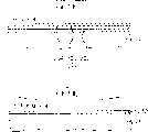
下一步,对第二个方面进行解释。图2A和图2B是用于解释第二个方面的示意图。此处,使用在存储单元区域中形成ONO膜,而在外围电路区域中形成栅绝缘膜的实例来进行解释。Next, explain the second aspect. 2A and 2B are schematic diagrams for explaining the second aspect. Here, an example is explained using an example in which an ONO film is formed in a memory cell region and a gate insulating film is formed in a peripheral circuit region.
首先,如图2A所示,在本实施例中,通过上述的等离子氮化方法,对作为硅半导体衬底的存储单元区域,或者作为存储单元区域中的多晶硅膜或者a-Si膜(例如,岛形浮栅)的硅区域201的表面层进行完全氮化,从而形成氮化硅膜202。优选的是在530℃或者更低的温度下,例如400℃的温度条件下进行处理。低温处理可防止氮化硅膜中的氢释放并扩散到下层二氧化硅膜中。另外,仅生成N*基作为自由基,可以不使用氢作为原料气体而进行等离子体处理。First, as shown in FIG. 2A, in this embodiment, by the above-mentioned plasma nitridation method, the memory cell region as the silicon semiconductor substrate, or the polysilicon film or a-Si film (for example, The surface layer of the
然后,如图2B所示,通过上述的等离子氧化方法对氮化硅膜202的表面层进行氧化。通过上述的等离子氮化方法形成厚度为15nm或更薄的氮化硅膜202,从而不仅对氮化硅膜202的表面层进行氧化,而且对硅区域201与氮化硅膜202的界面进行氧化。从而,形成由下层二氧化硅膜203、氮化硅膜202和上层二氧化硅膜204构成的作为多层绝缘膜的ONO膜211。当形成下层二氧化硅膜203和上层二氧化硅膜204时,优选的是在530℃或更低的温度下,例如400℃的温度条件下进行处理。另外,仅生成O*基作为自由基,可以不使用氢作为原料气体而进行等离子体处理。Then, as shown in FIG. 2B, the surface layer of the
此时,与第一个实施例相似,通过上述的等离子氧化方法,在形成下层二氧化硅膜203和上层二氧化硅膜204的同时,在半导体衬底的外围电路区域中形成栅绝缘膜212。这使得热历史更低,时间更短,从而使得元件更小。在此情况下,与在形成ONO膜之后形成外围电路区域中的栅绝缘膜的情况不同,在形成ONO膜211时(在已经形成氮化硅膜202的状态下),通过用于形成下层二氧化硅膜203和上层二氧化硅膜204的等离子氧化而同时形成栅绝缘膜212。因此,可以利用由等离子氧化所形成的强氧化能力。At this time, similar to the first embodiment, by the above-mentioned plasma oxidation method, while forming the lower
在本实施例中,当形成ONO膜时,不使用CVD方法而直接由硅形成氮化膜和氧化膜。因此,可以形成具有低泄漏电流和很高质量的ONO膜。In this embodiment, when forming the ONO film, the nitride film and the oxide film are formed directly from silicon without using the CVD method. Therefore, an ONO film with low leakage current and very high quality can be formed.
—第三个方面——The third aspect—
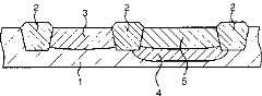
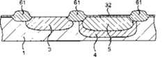
下一步,对第三个方面进行解释。图3A和图3B是用于解释第三个方面的示意图。此处,同样使用在存储单元区域中形成ONO膜,而在外围电路区域中形成栅绝缘膜的实例来进行解释。Next, explain the third aspect. 3A and 3B are schematic diagrams for explaining the third aspect. Here, too, an example is explained using an example in which an ONO film is formed in a memory cell region and a gate insulating film is formed in a peripheral circuit region.
首先,如图3A所示,在本实施例中,当在作为硅半导体衬底的存储单元区域,或者作为存储单元区域中的多晶硅膜或者a-Si膜(例如,岛形浮栅)的硅区域301上形成下层二氧化硅膜302之后,通过(例如)热CVD方法或者等离子体CVD方法等等在下层二氧化硅膜302上形成氮化硅膜303。由CVD方法形成的氮化硅膜包含很多晶格缺陷,因此,其适用于电荷存储膜。First, as shown in FIG. 3A , in the present embodiment, when the memory cell region as a silicon semiconductor substrate, or the silicon film as a polysilicon film or a-Si film (for example, an island-shaped floating gate) in the memory cell region After the lower
然后,如图3B所示,通过上述的等离子氧化方法,对氮化硅膜303的表面层进行氧化,从而置换为上层二氧化硅膜304。从而,形成了由下层二氧化硅膜302、氮化硅膜303和上层二氧化硅膜304构成的作为多层绝缘膜的ONO膜311。当形成上层二氧化硅膜304时,优选的是在530℃或更低的温度下,例如400℃的温度条件下进行处理。另外,仅生成O*基作为自由基,可以不使用氢作为原料气体而进行等离子体处理。Then, as shown in FIG. 3B, the surface layer of the
此时,通过上述的等离子氧化方法,在形成上层二氧化硅膜304的同时,在半导体衬底的外围电路区域中形成栅绝缘膜312。这使得热历史更低,时间更短,从而使得元件更小。在此情况下,与在形成ONO膜之后形成外围电路区域中的栅绝缘膜的情况不同,在形成ONO膜311时(在已经形成下层二氧化硅膜302和氮化硅膜303的状态下),通过用于形成上层二氧化硅膜304的等离子氧化而同时形成栅绝缘膜312。因此,可以利用由等离子氧化所形成的强氧化能力。At this time, the
—具体实施例—- specific embodiment -
下面基于本发明的上述基本结构对具体实施例进行解释。Specific embodiments are explained below based on the above basic structure of the present invention.
—第一个实施例—— FIRST EMBODIMENT —
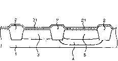
在本实施例中,对具有内建位线型SONOS结构的半导体存储器件进行解释。为方便起见,通过其制造方法对该半导体存储器件的结构进行解释。In this embodiment, a semiconductor memory device having a built-in bit line type SONOS structure is explained. For convenience, the structure of the semiconductor memory device is explained by its manufacturing method.
本半导体存储器件的结构为:存储单元区域中的SONOS晶体管为平面型,在外围电路区域中形成CMOS晶体管。The structure of the semiconductor memory device is that the SONOS transistors in the memory cell area are planar, and the CMOS transistors are formed in the peripheral circuit area.
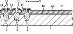
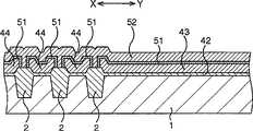
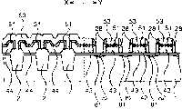
图4A至图13B是示意截面图,按照工艺顺序显示了在这个实施例中制造包含内建位线型SONOS晶体管的半导体存储器件的方法。其中,各个图中的A表示的是存储单元区域(核心区域),而B表示的是外围电路区域。A的左侧对应于与栅极(字线)平行的横截面(X截面),A的右侧对应于与栅极(字线)垂直的横截面(Y截面)。4A to 13B are schematic cross-sectional views showing, in process order, a method of manufacturing a semiconductor memory device including a built-in bit line type SONOS transistor in this embodiment. Among them, A in each figure indicates the memory cell area (core area), and B indicates the peripheral circuit area. The left side of A corresponds to a cross section (X section) parallel to the gate (word line), and the right side of A corresponds to a cross section (Y section) perpendicular to the gate (word line).
首先,如图4A和图4B所示,在外围电路区域12中形成单元隔离结构,以划分单元活动区域。First, as shown in FIGS. 4A and 4B , a cell isolation structure is formed in the peripheral circuit region 12 to divide the cell active region.
此处,通过所谓的STI(Shallow Trench Isolation,浅沟槽隔离)方法,在p型硅半导体衬底1的外围电路区域12的单元隔离区域中形成沟槽。另外,使用绝缘体对沟槽进行填充而形成STI单元隔离结构2,从而划分单元活动区域。顺便提及,由于本实施例中公布的是平面型存储器,所以在核心区域没有形成单元隔离结构。Here, trenches are formed in the cell isolation region of the peripheral circuit region 12 of the p-type
然后,在外围电路区域12中形成阱3、4和5。Then,
具体而言,在n型区域中,仅将诸如磷(P)、砷(As)等等的n型杂质离子注入到外围电路区域12的n型区域中,并且通过退火处理使杂质热扩散,以在n型区域中形成n阱3。另一方面,在p型区域中,仅将诸如磷(P)、砷(As)等等的n型杂质离子较深地注入到外围电路区域12的p型区域中,而与n型杂质相比,较浅地注入诸如硼(B)等的p型杂质离子。然后,通过退火处理使杂质热扩散,以形成较深的n阱4并在n阱4中形成p阱5,从而在p型区域中形成三阱结构。Specifically, in the n-type region, only n-type impurity ions such as phosphorus (P), arsenic (As), etc. are implanted into the n-type region of the peripheral circuit region 12, and the impurities are thermally diffused by annealing, to form an n well 3 in the n-type region. On the other hand, in the p-type region, only n-type impurity ions such as phosphorous (P), arsenic (As), etc. are implanted deeply into the p-type region of the peripheral circuit region 12, and In comparison, p-type impurity ions such as boron (B) are shallowly implanted. Then, the impurities are thermally diffused by annealing to form a deeper n-well 4 and a p-well 5 in the n-well 4, thereby forming a triple-well structure in the p-type region.
然后,在半导体衬底1的核心区域11中形成位线扩散层6。Then, bit
具体而言,通过光刻而形成位线形状的抗蚀剂掩模(未显示),并且将其作为掩模,进行n型杂质的离子注入,在本实施例中,n型杂质为砷(As)。此处,离子注入的剂量为2.0×10¹⁴(/cm2)或者更高,以降低位线电阻。通过这些处理,形成了也作为源极/漏极的位线扩散层6。Specifically, a resist mask (not shown) in the shape of a bit line is formed by photolithography, and using this as a mask, ion implantation of an n-type impurity, which in this embodiment is arsenic ( As). Here, the dose of ion implantation is 2.0×10¹⁴ (/cm2 ) or higher in order to reduce bit line resistance. Through these treatments, the bit
然后,在通过灰化处理等等而去除抗蚀剂掩模之后,形成仅覆盖外围电路区域12的p型区域的抗蚀剂掩模(未显示)。另外,将其作为掩模,进行作为阈值调节的硼(B)离子注入(参见标号41)。顺便提及,此离子注入不限于p型区域,而可以用于n型区域。Then, after the resist mask is removed by an ashing process or the like, a resist mask (not shown) covering only the p-type region of the peripheral circuit region 12 is formed. In addition, using this as a mask, boron (B) ion implantation (refer to reference numeral 41 ) is performed as a threshold value adjustment. Incidentally, this ion implantation is not limited to the p-type region but can be used for the n-type region.
然后,在通过灰化处理等等而去除抗蚀剂掩模,并且通过HF处理而露出核心区域11和外围电路区域12中各个单元活动区域的硅表面之后,形成作为多层绝缘膜的ONO膜。Then, after removing the resist mask by ashing treatment or the like, and exposing the silicon surface of each cell active region in the core region 11 and the peripheral circuit region 12 by HF treatment, an ONO film as a multilayer insulating film is formed .
此处,通过微波激励而使用等离子氧化方法和等离子氮化方法来形成ONO膜。Here, the ONO film is formed using a plasma oxidation method and a plasma nitridation method by microwave excitation.
具体而言,如图14所示,将具有径向线隙缝天线的等离子处理器用于等离子氧化和氮化。此等离子体处理器1000包括与聚集工具1001相连的闸阀1002;处理室1005,其中,处理室1005能够容纳一个基座,在基座上安装所要进行处理的物体(在本实施例中为半导体衬底1),并且基座具有冷却套管1003,用于在进行等离子体处理时对所处理的物体进行冷却;与处理室1005相连的高真空泵1006;微波供应源1010;天线部件1020;与天线部件1020一起构成离子涂镀设备的偏压高频电源1007和匹配箱1008;具有供气环路1031、1041的供气系统1030、1040;以及用于控制所要处理物体的温度的温度控制部分1050。Specifically, as shown in FIG. 14, a plasma processor with a radial line slot antenna was used for plasma oxidation and nitridation. This
微波供应源1010由(例如)磁控管构成,通常能够生成2.45GHz的微波(例如,5kW)。然后通过波型转换器1012将微波的传输波型转换为TM、TE、TEM等等。The
天线部件1020具有温度调节板1022、安装部分1023和介电板。将温度调节板1022连接到温度控制单元1021,而安装部分1023容纳波长缩短材料1024和与微波缩短材料1024接触的槽隙电极(slot electrode)(未显示)。将此槽隙电极称为径向线隙缝天线(radial line slotantenna,RLSA)或者超高效率平面天线。然而,在本实施例中,可以使用不同类型的天线,例如,单层波导平面天线、介电基板平行板隙缝天线阵等等。The
如图5A和图5B所示,在使用上述结构的等离子体处理器形成本实施例的ONO膜时,首先通过等离子氧化方法在单元活动区域的硅表面上形成下层二氧化硅膜21。As shown in FIG. 5A and FIG. 5B , when the ONO film of this embodiment is formed using the plasma processor of the above structure, the lower
具体而言,使用包含Ar和O2但不包含氢的源气体,通过在450℃的温度条件下,使用3.5kW的微波对源气体进行照射而生成氧基(O*),进行氧化处理,从而形成下层二氧化硅膜21。应当注意,可以使用热氧化方法或者CVD氧化方法而不是等离子氧化方法而形成下层二氧化硅膜。Specifically, using a source gas containing Ar and O2 but not containing hydrogen, the source gas was irradiated with a microwave of 3.5 kW at a temperature of 450°C to generate oxygen groups (O*), and oxidation treatment was performed, Thus, an underlying
然后,如图6A和图6B所示,使用SiH4为原料气体,在530℃的温度条件下,通过热CVD方法在下层二氧化硅膜21上形成大约9nm厚的非晶硅(a-Si)膜31。此处,可以形成多晶硅膜而不是a-Si膜。Then, as shown in FIG. 6A and FIG. 6B, using SiH4 as the raw material gas, under the temperature condition of 530° C., an amorphous silicon (a-Si )
下一步,如图7A和图7B所示,通过等离子氮化方法对a-Si膜31进行完全氮化,从而在下层二氧化硅膜21上形成氮化硅膜22。Next, as shown in FIGS. 7A and 7B , the
具体而言,使用包含N2和Ar但不包含氢的源气体,通过在450℃的温度条件下,使用3.5kW的微波对源气体进行照射而生成氮基(N*),从而进行氮化处理。膜厚度大约为9nm的a-Si膜31被完全氮化,从而置换为厚度大约为18nm的氮化硅膜22。Specifically, nitrogen radicals (N*) are generated by irradiating the source gas with a microwave of 3.5 kW at a temperature of 450°C using a source gas containingN2 and Ar but not containing hydrogen. deal with. The
然后,通过等离子氧化方法对氮化硅膜22的表面层进行氧化,以形成上层二氧化硅膜。在本实施例中,通过等离子氧化,在核心区域11中形成上层二氧化硅膜的同时,分别在外围电路区域12中形成栅绝缘膜。Then, the surface layer of the
具体而言,如图8A和8B所示,仅在核心区域11上覆盖抗蚀剂掩模(未显示),并且将其作为掩模,通过干蚀刻而去除在外围电路区域12中所形成的氮化硅膜22。然后,通过HF处理而去除在外围电路区域12中所形成的下层二氧化硅膜21,从而露出外围电路区域12中的半导体衬底1的表面。Specifically, as shown in FIGS. 8A and 8B , only the core region 11 is covered with a resist mask (not shown), and using it as a mask, the circuit formed in the peripheral circuit region 12 is removed by dry etching.
然后,如图9A和图9B所示,在通过灰化处理或者类似的处理而去除抗蚀剂掩模之后,使用包含Ar和O2但不包含氢的源气体,通过在450℃的温度条件下,使用3.5kW的微波对源气体进行照射而生成氧基(O*),进行氧化处理。通过对核心区域11中的氮化硅膜22的表面层进行氧化而形成二氧化硅膜30。同时,在外围电路区域12中,形成了膜厚度大约为8nm的二氧化硅膜32。Then, as shown in FIGS. 9A and 9B , after removing the resist mask by ashing treatment or the like, using a source gas containing Ar and O2 but not containing Next, the source gas was irradiated with microwaves of 3.5 kW to generate oxygen radicals (O*) for oxidation treatment.
然后,如图10A和图10B所示,在外围电路区域12中形成用于形成薄栅绝缘膜的部分,即仅露出n型区域的抗蚀剂掩模(未显示)。将其作为掩模而进行HF处理,从而去除n型区域中的二氧化硅膜32。Then, as shown in FIGS. 10A and 10B , a resist mask (not shown) that exposes only the n-type region is formed in the peripheral circuit region 12 for forming a thin gate insulating film. Using this as a mask, HF treatment is performed to remove the
然后,如图11A和11B所示,在通过灰化处理或者类似处理而去除抗蚀剂掩模之后,使用上述的等离子氧化方法进行氧化处理,从而在露出的半导体衬底1的表面上,形成膜厚度大约为7nm的二氧化硅膜。此时,在核心区域11中,氮化硅膜22的表面层被进一步氧化,从而置换为二氧化硅膜,结果,形成了膜厚度大约为10nm的上层二氧化硅膜23。同时,在外围电路区域12中,在n型区域中形成了膜厚度大约为7nm的薄栅绝缘膜24。另外,在上述8nm膜厚的等离子氧化(二氧化硅膜32)之后,通过大约7nm膜厚的等离子氧化,在p型区域中形成膜厚度大约为13nm的栅绝缘膜25。Then, as shown in FIGS. 11A and 11B , after removing the resist mask by ashing treatment or the like, oxidation treatment is performed using the above-mentioned plasma oxidation method, so that on the exposed surface of the
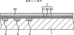
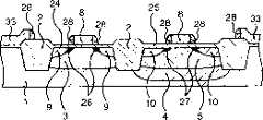
从而,在核心区域11中,ONO膜7具有通过等离子氧化形成的膜厚度大约为8nm的下层二氧化硅膜21;通过等离子氮化形成的膜厚度大约为8nm的氮化硅膜22,其作为电荷存储膜,且其表面层由等离子氧化两次削减;以及通过等离子氧化形成的上层二氧化硅膜23。另一方面,在外围电路区域12中,分别在n型区域中形成膜厚度大约为8nm的薄栅绝缘膜24,在p型区域中形成膜厚度大约为13nm的栅绝缘膜25。Thus, in the core region 11, the
然后,如图12A和图12B所示,通过CVD方法在核心区域11和外围电路区域12的整个表面上形成多晶硅膜33。Then, as shown in FIGS. 12A and 12B ,
然后,如图13A和图13B所示,通过光刻,然后干蚀刻,在多晶硅膜33上形成图案,从而分别在核心区域11、外围电路区域12的n型区域和p型区域中形成栅极8。此时,核心区域11中的这些栅极8大致垂直地与位线扩散层6交叉。Then, as shown in FIGS. 13A and 13B , by photolithography and then dry etching, the
然后,仅在外围电路区域12中形成源极/漏极9和10。Then, the source/
具体而言,将n型杂质离子注入到n型区域中栅极8两侧的半导体衬底1的表面,以形成外延区26。同时,在p型区域中,将p型杂质离子注入到栅极8两侧的半导体衬底1的表面,以形成外延区27。Specifically, n-type impurity ions are implanted into the surface of the
下一步,在通过CVD方法在整个表面上沉积二氧化硅膜之后,对该二氧化硅膜的整个表面进行各向异性蚀刻(深蚀刻,etch back),以仅在各个栅极8的两侧留下二氧化硅膜,从而形成侧壁28。Next, after depositing a silicon dioxide film on the entire surface by the CVD method, anisotropic etching (etch back) is performed on the entire surface of the silicon dioxide film so that only on both sides of each
然后,在n型区域中,将n型杂质离子注入到栅极8和侧壁28两侧的半导体衬底1的表面中,以形成深源极/漏极9,其部分地与外延区26重叠。同时,在p型区域中,将p型杂质离子注入到栅极8和侧壁28两侧的半导体衬底1的表面中,以形成深源极/漏极10,其部分地与外延区27重叠。此时,可以露出源极/漏极9和10的表面,以通过硅化处理而在源极/漏极9和10上、以及外围电路区域12的栅极8上形成硅化层。Then, in the n-type region, n-type impurity ions are implanted into the surface of the
然后,形成覆盖整个表面、接触孔、通孔、各种类型的配线层等等的多层层间绝缘,并且在顶层形成保护绝缘层(均未显示),从而在半导体衬底1上形成了许多具有包含SONOS型存储单元和CMOS晶体管的外围电路的半导体存储器件。然后,通过对上述器件进行分离和封装,可以制造单独的半导体存储器件。Then, a multilayer interlayer insulation covering the entire surface, contact holes, via holes, various types of wiring layers, etc. is formed, and a protective insulating layer (none of them is shown) is formed on the top layer, thereby forming on the
如上所述,根据本发明,在低温下形成高质量的作为电荷存储膜的ONO膜7,另外,在形成ONO膜7时,成功地在外围电路中形成了栅绝缘膜24和25。这使得能够以高质量和低成本而实现SONOS型的半导体存储器件。As described above, according to the present invention, high-
—第二个实施例—— SECOND EMBODIMENT —
在本实施例中,对浮栅型半导体存储器件进行描述。为方便起见,通过其制造方法对该半导体存储器件的结构进行解释。In this embodiment, a floating gate type semiconductor memory device is described. For convenience, the structure of the semiconductor memory device is explained by its manufacturing method.
在存储单元区域中形成浮栅型晶体管,而在外围电路区域中形成CMOS晶体管。Floating gate type transistors are formed in the memory cell region, and CMOS transistors are formed in the peripheral circuit region.
图15A至图26B是示意截面图,按照工艺顺序显示了在第二个实施例中制造包含浮栅型晶体管的半导体存储器件的方法。应当注意,为了方便,用相同的标号表示与第一个实施例相同或者类似的部分。此处,除了图20以外,其他各个图中的A部分显示的是存储单元区域(核心区域),而B部分显示的是外围电路部分。A部分的左侧对应于与栅极(字线)平行的截面(X截面),A部分的右侧对应于与栅极(字线)垂直的截面(Y截面)。图20对应于X截面。15A to 26B are schematic cross-sectional views showing a method of manufacturing a semiconductor memory device including floating gate type transistors in the second embodiment in process order. It should be noted that, for convenience, the same reference numerals are used to designate the same or similar parts as those of the first embodiment. Here, in each figure except FIG. 20 , part A shows the memory cell region (core region), and part B shows the peripheral circuit part. The left side of part A corresponds to a cross section (X cross section) parallel to the gate (word line), and the right side of part A corresponds to a cross section (Y cross section) perpendicular to the gate (word line). Fig. 20 corresponds to the X section.
首先,如图15A和图15B所示,分别在核心区域11和外围电路区域12中形成单元隔离结构,以划分单元活动区域。First, as shown in FIGS. 15A and 15B , cell isolation structures are formed in the core region 11 and the peripheral circuit region 12 respectively to divide cell active regions.
此处,通过所谓的STI(浅沟槽隔离)方法,在p型硅半导体衬底1的核心区域11和外围电路区域12的单元隔离区域中形成沟槽。另外,通过使用绝缘体对沟槽进行填充而形成STI单元隔离结构2,从而划分单元活动区域。Here, trenches are formed in the cell isolation regions of the core region 11 and the peripheral circuit region 12 of the p-type
然后,在外围电路区域12中形成阱3、4和5。Then,
具体而言,在n型区域中,仅将诸如磷(P)、砷(As)等等的n型杂质离子注入到外围电路区域12的n型区域中,并且通过退火处理使杂质热扩散,以在n型区域中形成n阱3。另一方面,在p型区域中,仅将诸如磷(P)、砷(As)等等的n型杂质离子较深地注入到外围电路区域12的p型区域,与n型杂质相比,对诸如硼(B)等的p型杂质进行较浅的离子注入。然后,通过退火处理使杂质热扩散,以形成较深的n阱4并在n阱4中形成p阱5,从而在p型区域中形成三阱结构。Specifically, in the n-type region, only n-type impurity ions such as phosphorus (P), arsenic (As), etc. are implanted into the n-type region of the peripheral circuit region 12, and the impurities are thermally diffused by annealing, to form an n well 3 in the n-type region. On the other hand, in the p-type region, only n-type impurity ions such as phosphorus (P), arsenic (As), etc. are implanted deeply into the p-type region of the peripheral circuit region 12, compared with n-type impurities, Shallow ion implantation is performed for p-type impurities such as boron (B). Then, the impurities are thermally diffused by annealing to form a deeper n-well 4 and a p-well 5 in the n-well 4, thereby forming a triple-well structure in the p-type region.
然后,形成仅覆盖外围电路区域12的p型区域的抗蚀剂掩模(未显示)。另外,将其作为掩模,进行用于阈值调节的硼(B)离子注入(参见标号41)。顺便提及,此离子注入不限于p型区域,而且可以用于n型区域。Then, a resist mask (not shown) covering only the p-type region of the peripheral circuit region 12 is formed. In addition, using this as a mask, boron (B) ion implantation (see reference numeral 41) for threshold value adjustment is performed. Incidentally, this ion implantation is not limited to the p-type region, but can be used for the n-type region.
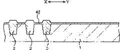
然后,如图16A和图16B所示,在通过灰化处理或者类似处理而去除抗蚀剂掩模之后,通过HF处理而露出核心区域11和外围电路区域12中各个单元活动区域的硅表面。然后,通过热氧化而在各个单元活动区域中形成膜厚度大约为10nm的隧道氧化膜42。为了降低温度,可以使用上述的等离子氧化方法而不是热氧化方法来形成隧道氧化膜。Then, as shown in FIGS. 16A and 16B , after the resist mask is removed by an ashing process or the like, the silicon surface of each cell active area in the core region 11 and the peripheral circuit region 12 is exposed by an HF process. Then, a
然后,如图17A和图17B所示,将SiH4和PH3作为原料气体,在530℃的温度条件下,使用热CVD方法,整体地沉积一层通过掺磷(P)而形成的非晶硅(a-Si),膜厚度大约为90nm。Then, as shown in FIG. 17A and FIG. 17B , using SiH4 and PH3 as raw material gases, at a temperature of 530°C, using a thermal CVD method, a layer of amorphous formed by doping phosphorus (P) is deposited as a whole. Silicon (a-Si), the film thickness is about 90nm.
然后,如图18A和图18B所示,通过光刻,然后干蚀刻,在a-Si膜43上形成图案,以形成浮栅44,这些浮栅44分别在垂直于下面所述的字线的方向上划分。同时,在外围电路区域12中,整体地保留了a-Si膜43。Then, as shown in FIGS. 18A and 18B, the
然后,形成多层绝缘膜的ONO膜,作为介电膜。Then, an ONO film of a multilayer insulating film is formed as a dielectric film.
首先,如图19A和图19B所示,使用上述的等离子氮化方法形成氮化硅膜45。First, as shown in FIGS. 19A and 19B , a
具体而言,与第一个实施例的情况相同,使用图14所示的具有径向线隙缝天线的等离子体处理器,并且使用包含Ar和N2但不包含氢的源气体,在450℃的温度条件下,使用3.5kW的微波对源气体进行照射而生成氮基(N*),进行氮化处理,以形成膜厚度大约为12nm的氮化硅膜45。Specifically, as in the case of the first embodiment, using a plasma processor havinga radial line slot antenna shown in FIG. Under the temperature conditions of 3.5 kW, the source gas is irradiated with microwaves of 3.5 kW to generate nitrogen radicals (N*), and a nitriding treatment is performed to form a
然后,如图20所示,使用上述的等离子氧化方法,在氮化硅膜45的上面和下面同时形成下层二氧化硅膜46和上层二氧化硅膜47。Then, as shown in FIG. 20, a lower silicon dioxide film 46 and an upper silicon dioxide film 47 are simultaneously formed on and under the
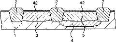
具体而言,使用包含Ar和O2但不包含氢的源气体,在450℃的温度条件下,使用3.5kW的微波对源气体进行照射而生成氧基(O*),从而进行氧化处理。通过把a-Si膜43与氮化硅膜45面对的厚度大约为4nm的界面置换为氧化膜而形成下层二氧化硅膜46。同时,通过把氮化硅膜45的厚度大约为5nm的上层置换为氧化膜而形成上层二氧化硅膜47。此时,在核心区域11中形成了ONO膜51,其包括浮栅44上的厚度大约为4nm的下层二氧化硅膜46,浮栅44的膜厚度由上述的等离子氮化和等离子氧化处理而降低为大约81nm;氮化硅膜45,其膜厚度降低到大约6nm;以及厚度大约为4nm的上层二氧化硅膜47。应当注意,为方便起见,在图21A至图26B,将三层45、46和47简化显示为单层ONO膜51。Specifically, using a source gas containing Ar and O2 but not containing hydrogen, the source gas was irradiated with a microwave of 3.5 kW at a temperature of 450° C. to generate oxygen groups (O*) for oxidation treatment. The lower silicon dioxide film 46 is formed by replacing the interface having a thickness of about 4 nm where the
然后,如图21A和图21B所示,通过干蚀刻而去除外围电路区域12中的ONO膜51和a-Si膜43。另外,通过HF处理而露出外围电路区域12中的单元活动区域的硅表面。Then, as shown in FIGS. 21A and 21B , the
然后,如图22A和图22B所示,对外围电路区域12中的单元活动区域的硅表面进行热氧化,以形成厚度大约为8nm的二氧化硅膜48。此时,热氧化方法的氧化能力不是很大,可以忽略核心区域11中ONO膜51的氧化。Then, as shown in FIGS. 22A and 22B, the silicon surface of the cell active region in the peripheral circuit region 12 is thermally oxidized to form a
然后,如图23A和图23B所示,通过HF处理,去除用于形成外围电路区域12中的薄栅绝缘膜的部分,在本例中为n型区域中的二氧化硅膜48。Then, as shown in FIGS. 23A and 23B , a portion for forming the thin gate insulating film in the peripheral circuit region 12 , in this example, the
然后,如图24A和图24B所示,进行热氧化,以在外围电路区域12的n型和p型区域的硅表面上形成厚度大约为7nm的二氧化硅膜。在n型区域中形成厚度大约为10nm的薄栅绝缘膜49。另外,在进行上述的膜厚度为8nm的热氧化之后,进行膜厚度大约为10nm的热氧化,使得在p型区域中形成厚度大约为16nm的栅绝缘膜50。Then, as shown in FIGS. 24A and 24B , thermal oxidation is performed to form a silicon dioxide film with a thickness of about 7 nm on the silicon surface of the n-type and p-type regions of the peripheral circuit region 12 . A thin
然后,如图25A和图25B所示,在通过CVD方法在整个表面上沉积一层a-Si膜52之后,如图26A和图26B所示,通过光刻,然后干蚀刻,在a-Si膜52(以及核心区域11中的a-Si膜43)上形成图案。在核心区域11中,形成控制栅53,其作为字线,通过作为介电膜的ONO膜51而与浮栅44进行电容耦合。在外围电路区域12中,形成作为CMOS晶体管一部分的栅极54。此时,通过对a-Si膜52进行干蚀刻,在形成控制栅53的同时,去除控制栅53从浮栅44中凸出的部分。Then, as shown in FIGS. 25A and 25B, after depositing a layer of
然后,仅在核心区域1 1中形成外延区81。Then,
具体而言,将n型杂质离子注入到控制栅53两侧的半导体衬底1的表面,以形成外延区81。Specifically, n-type impurity ions are implanted into the surface of the
然后,仅在外围电路区域12中形成外延区26和27。Then,
具体而言,在n型区域中,将n型杂质离子注入到栅极54两侧的半导体衬底1的表面,以形成外延区26。同时,在p型区域中,将p型杂质离子注入到栅极54两侧的半导体衬底1的表面,以形成外延区27。Specifically, in the n-type region, n-type impurity ions are implanted into the surface of the
下一步,在通过CVD方法在整个表面上沉积一层二氧化硅膜之后,对该二氧化硅膜的整个表面进行各向异性蚀刻(深蚀刻),以仅在各个栅极54的两侧留下二氧化硅膜,从而形成侧壁28。Next, after depositing a silicon dioxide film on the entire surface by the CVD method, the entire surface of the silicon dioxide film is anisotropically etched (etched back) to leave only the two sides of each
然后,在核心区域11中,将n型杂质离子注入到控制栅53和侧壁28两侧的半导体衬底1的表面中,以形成源极/漏极82,其部分地与外延区81重叠。Then, in the core region 11, n-type impurity ions are implanted into the surface of the
然后,在外围电路区域12中,在n型区域中,将n型杂质离子注入到栅极54和侧壁28两侧的半导体衬底1的表面中,以形成深源极/漏极9,其部分地与外延区26重叠。同时,在p型区域中,将p型杂质离子注入到栅极54和侧壁28两侧的半导体衬底1的表面中,以形成深源极/漏极10,其部分地与外延区27重叠。此时,可以露出源极/漏极9和10的表面,以通过硅化处理,在源极/漏极9和10上、以及外围电路区域12的栅极54上形成硅化层。Then, in the peripheral circuit region 12, in the n-type region, n-type impurity ions are implanted into the surface of the
然后,形成覆盖整个表面、接触孔、通孔、各种类型的配线层等等的多层层间绝缘,并且在顶层形成保护绝缘膜(均未显示),从而在半导体衬底1上形成了许多具有包含浮栅型存储单元和CMOS晶体管的外围电路的半导体存储器件。然后,通过对上述器件进行分离和封装,可以制造单独的半导体存储器件。Then, a multilayer interlayer insulation covering the entire surface, contact holes, via holes, various types of wiring layers, etc. is formed, and a protective insulating film (none of them is shown) is formed on the top layer, thereby forming on the
如上所述,根据本实施例,在低温下形成高质量的作为介电膜的ONO膜51,另外,同时形成氮化硅膜上面和下面的二氧化硅膜。这减少了处理的次数,并使得能够实现高可靠性和低成本的浮栅型半导体存储器件。As described above, according to the present embodiment, the high-
—第三个实施例—— THIRD EMBODIMENT —
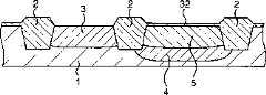
在本实施例中,对具有内建位线型SONOS结构的半导体存储器件进行描述。为方便起见,通过其制造方法对该半导体存储器件的结构进行解释。In this embodiment, a semiconductor memory device having a built-in bit line type SONOS structure is described. For convenience, the structure of the semiconductor memory device is explained by its manufacturing method.
本半导体存储器件的结构为:存储单元区域中的SONOS晶体管为平面型,在外围电路区域中形成有CMOS晶体管。The structure of the semiconductor memory device is that the SONOS transistors in the memory cell area are planar, and the CMOS transistors are formed in the peripheral circuit area.
图27A至图35B是示意截面图,按照工艺顺序显示了在第三个实施例中制造包含内建位线型SONOS晶体管的半导体存储器件的方法。应当注意,为了方便,用相同的标号指示与第一个实施例相同或者类似的部分。此处,各个图中的A部分显示的是存储单元区域(核心区域),而B部分显示的是外围电路区域。A部分的左侧对应于与栅极(字线)平行的截面(X截面),A部分的右侧对应于与栅极(字线)垂直的截面(Y截面)。27A to 35B are schematic cross-sectional views showing a method of manufacturing a semiconductor memory device including a built-in bit line type SONOS transistor in the third embodiment in process order. It should be noted that, for convenience, the same reference numerals are used to designate the same or similar parts as those of the first embodiment. Here, part A in each figure shows the memory cell region (core region), and part B shows the peripheral circuit region. The left side of part A corresponds to a cross section (X cross section) parallel to the gate (word line), and the right side of part A corresponds to a cross section (Y cross section) perpendicular to the gate (word line).
首先,如图27A和图27B所示,在外围电路区域12中形成阱3、4和5。First, as shown in FIGS. 27A and 27B ,
具体而言,在n型区域中,仅将诸如磷(P)、砷(As)等等的n型杂质离子注入到外围电路区域12的n型区域中,并且通过退火处理使杂质热扩散,以在n型区域中形成n阱3。另一方面,在p型区域中,仅将诸如磷(P)、砷(As)等等的n型杂质离子较深地注入到外围电路区域12的p型区域中,与n型杂质相比,将诸如硼(B)等的p型杂质进行较浅的离子注入。然后,通过退火处理使杂质热扩散,以形成较深的n阱4并在n阱4中形成p阱5,从而在p型区域中形成三阱结构。Specifically, in the n-type region, only n-type impurity ions such as phosphorus (P), arsenic (As), etc. are implanted into the n-type region of the peripheral circuit region 12, and the impurities are thermally diffused by annealing, to form an n well 3 in the n-type region. On the other hand, in the p-type region, only n-type impurity ions such as phosphorus (P), arsenic (As), etc. , shallower ion implantation of p-type impurities such as boron (B). Then, the impurities are thermally diffused by annealing to form a deeper n-well 4 and a p-well 5 in the n-well 4, thereby forming a triple-well structure in the p-type region.
然后,在外围电路区域12中形成单元隔离结构,以划分单元活动区域。Then, a cell isolation structure is formed in the peripheral circuit area 12 to divide the cell active area.
此处,通过所谓的LOCOS方法,在p型硅半导体衬底1的外围电路区域12的单元隔离区域中形成场效氧化膜(field oxide film)61,以划分单元活动区域。顺便提及,由于在本实施例中对平面型存储器进行解释,所以在核心区域没有形成单元隔离结构。Here, a
然后,形成仅覆盖外围电路区域12的p型区域的抗蚀剂掩模(未显示)。另外,将其作为掩模,进行用于阈值调节的硼(B)离子注入(如标号41所示)。顺便提及,此离子注入不限于p型区域,而可以用于n型区域。Then, a resist mask (not shown) covering only the p-type region of the peripheral circuit region 12 is formed. In addition, using this as a mask, boron (B) ion implantation (shown by reference numeral 41) for threshold value adjustment is performed. Incidentally, this ion implantation is not limited to the p-type region but can be used for the n-type region.
然后,在半导体衬底1的核心区域11中形成位线扩散层6。Then, bit
具体而言,通过光刻而形成位线形状的抗蚀剂掩模(未显示),并且将其作为掩模,进行n型杂质的离子注入,在本实施例中,n型杂质为砷(As)。此处,离子注入的剂量为2.0×10¹⁴(/cm2)或者更高,以降低位线电阻。通过这些处理,形成了也作为源极/漏极的位线扩散层6。Specifically, a resist mask (not shown) in the shape of a bit line is formed by photolithography, and using this as a mask, ion implantation of an n-type impurity, which in this embodiment is arsenic ( As). Here, the dose of ion implantation is 2.0×10¹⁴ (/cm2 ) or higher in order to reduce bit line resistance. Through these treatments, the bit
然后,在通过灰化处理等等而去除抗蚀剂掩模,并且通过HF处理而露出核心区域11和外围电路区域12中各个单元活动区域的硅表面之后,形成作为多层绝缘膜的ONO膜。Then, after removing the resist mask by ashing treatment or the like, and exposing the silicon surface of each cell active region in the core region 11 and the peripheral circuit region 12 by HF treatment, an ONO film as a multilayer insulating film is formed .
具体而言,如图28A和图28B所示,通过上述的等离子氧化方法而在单元活动区域的硅表面上形成下层二氧化硅膜62。Specifically, as shown in FIGS. 28A and 28B, an underlying
具体而言,使用如图14所示的具有径向线隙缝天线的等离子体处理器,并且使用包含Ar和O2但不包含氢的源气体,在450℃的温度条件下,使用3.5kW的微波对源气体进行照射而生成氧基(O*),进行氧化处理,从而形成下层二氧化硅膜62。当使用等离子氧化方法而不是热氧化方法而形成下层二氧化硅膜62时,可以在低温下形成致密的膜,从而控制位线扩散层6的杂质扩散。Specifically, using a plasma processor with a radial line slot antenna as shown in Fig. 14, and using a source gas containing Ar andO2 but not containing hydrogen, a 3.5 kW The source gas is irradiated with microwaves to generate oxygen radicals (O*) and subjected to oxidation treatment to form the lower
然后,如图29A和图29B所示,通过热CVD方法而在下层二氧化硅膜62上形成氮化硅膜63。Then, as shown in FIGS. 29A and 29B, a
具体而言,在730℃的温度条件下,使用SiH2Cl2和NH3作为原料气体,通过热CVD方法沉积一层厚度大约为15nm的氮化硅膜63。此处,使用热CVD而不是等离子氮化,可以形成适用于SONOS型存储单元的作为具有许多陷阱(trap)的电荷存储膜的氮化硅膜。Specifically, a
然后,如图30A和图30B所示,仅在核心区域11上覆盖抗蚀剂掩模(未显示),并且将其作为掩模,通过干蚀刻而去除在外围电路区域12中形成的氮化硅膜63。然后,通过HF处理而去除在外围电路区域12中形成的下层二氧化硅膜62,从而露出外围电路区域12中的半导体衬底1的表面。Then, as shown in FIGS. 30A and 30B , only the core region 11 is covered with a resist mask (not shown), and using it as a mask, the nitride formed in the peripheral circuit region 12 is removed by dry etching.
然后,在通过灰化处理或者类似的处理而去除抗蚀剂掩模之后,通过等离子氧化方法而在核心区域11中形成上层二氧化硅膜64,在外围电路区域12中形成栅绝缘膜24和25。Then, after removing the resist mask by an ashing process or the like, an upper layer
具体而言,如图31A和图31B所示,使用包含Ar和O2但不包含氢的源气体,在450℃的温度条件下,使用3.5kW的微波对源气体进行照射而生成氧基(O*),进行氧化处理。通过对核心区域11中的氮化硅膜63的表面层进行氧化而形成二氧化硅膜70。同时,在外围电路区域12中形成膜厚度大约为8nm的二氧化硅膜32。Specifically, as shown in FIG. 31A and FIG. 31B , using a source gas containing Ar and O2 but not containing hydrogen, the source gas is irradiated with a microwave of 3.5 kW at a temperature of 450° C. to generate oxygen groups ( O*), for oxidation treatment.
然后,如图32A和图32B所示,在外围电路区域12中形成用于形成薄栅绝缘膜的部分,即仅露出n型区域的抗蚀剂掩模(未显示)。将其作为掩模进行HF处理,从而去除n型区域中的二氧化硅膜32。Then, as shown in FIGS. 32A and 32B , a resist mask (not shown) that exposes only the n-type region is formed in the peripheral circuit region 12 for forming a thin gate insulating film. HF treatment is performed using this as a mask, thereby removing
然后,如图33A和图33B所示,在通过灰化处理或者类似处理而去除抗蚀剂掩模之后,使用上述的等离子氧化方法进行氧化处理,从而在露出的半导体衬底1上形成膜厚度大约为7nm的二氧化硅膜。此时,在核心区域11中,氮化硅膜63的表面层被进一步氧化,从而被取代为二氧化硅膜,结果,形成了膜厚度大约为10nm的上层二氧化硅膜64。同时,在外围电路区域12中,在n型区域中形成膜厚度大约为7nm的薄栅绝缘膜24。另外,在p型区域中,在上述的膜厚度大约为8nm的等离子氧化之后,进行膜厚度大约为7nm的等离子氧化处理,从而形成膜厚度大约为13nm的栅绝缘膜25。Then, as shown in FIGS. 33A and 33B , after removing the resist mask by ashing treatment or the like, an oxidation treatment is performed using the above-mentioned plasma oxidation method to form a film thicker than the exposed
在核心区域11中形成了ONO膜71,其包括通过等离子氧化形成的膜厚度大约为8nm的下层二氧化硅膜62;通过热CVD形成的膜厚度大约为10nm的氮化硅膜63,其作为电荷存储膜,且其表面层由等离子氧化两次削减;以及通过等离子氧化形成的上层二氧化硅膜64。另一方面,在外围电路区域12中,分别在n型区域中形成膜厚度大约为8nm的薄栅绝缘膜24,在p型区域中形成膜厚度大约为13nm的栅绝缘膜25。In the core region 11, an
然后,如图34A和图34B所示,在核心区域11和外围电路区域12的整个表面上,通过CVD方法,首先形成多晶硅膜33,然后形成硅化钨膜72。Then, as shown in FIGS. 34A and 34B , on the entire surfaces of the core region 11 and the peripheral circuit region 12 , by the CVD method, first a
然后,如图35A和图35B所示,通过光刻,然后干蚀刻,在多晶硅膜33和硅化钨膜72上形成图案,从而分别在核心区域11、外围电路区域12的n型区域和p型区域中形成栅极73。此时,核心区域11中的这些栅极73大致垂直地与位线扩散层6交叉。Then, as shown in FIG. 35A and FIG. 35B, by photolithography and then dry etching, a pattern is formed on the
然后,仅在外围电路区域12中形成源极/漏极9和10。Then, the source/
具体而言,将n型杂质离子注入到n型区域的栅极73两侧的半导体衬底1的表面中,以形成外延区26。同时,在p型区域中,将p型杂质离子注入到栅极73两侧的半导体衬底1的表面中,以形成外延区27。Specifically, n-type impurity ions are implanted into the surface of the
下一步,在通过CVD方法在整个表面上沉积一层二氧化硅膜之后,对二氧化硅膜的整个表面进行各向异性蚀刻(深蚀刻),以仅在各个栅极73的两侧留下二氧化硅膜,从而形成侧壁28。Next, after depositing a silicon dioxide film on the entire surface by the CVD method, anisotropic etching (etching back) is performed on the entire surface of the silicon dioxide film to leave only on both sides of each
然后,在n型区域中,将n型杂质离子注入到栅极73和侧壁28两侧的半导体衬底1的表面中,以形成深源极/漏极9,其部分地与外延区26重叠。同时,在p型区域中,将p型杂质离子注入到栅极73和侧壁28两侧的半导体衬底1的表面中,以形成深源极/漏极10,其部分地与外延区27重叠。Then, in the n-type region, n-type impurity ions are implanted into the surface of the
然后,形成覆盖整个表面、接触孔、通孔、各种类型的配线层等等的多层层间绝缘,并且在顶层形成保护绝缘膜(均未显示),从而在半导体衬底1上形成了许多具有包含SONOS型存储单元和CMOS晶体管的外围电路的半导体存储器件。然后,通过对上述器件进行分离和封装,可以制造单独的半导体存储器件。Then, a multilayer interlayer insulation covering the entire surface, contact holes, via holes, various types of wiring layers, etc. is formed, and a protective insulating film (none of them is shown) is formed on the top layer, thereby forming on the
如上所述,根据本实施例,高质量地形成了作为电荷存储膜的ONO膜71,同时保持了高的电荷存储功能,另外,与ONO膜71同时形成了外围电路中的栅绝缘膜。这使得可以实现高可靠性和低成本的SONOS型半导体存储器件。As described above, according to the present embodiment, the
应当注意,本发明不局限于上述的实施例。例如,在如上所述的实施例中,将ONO膜解释为多层绝缘膜;然而,该实施例也适用于由二氧化硅膜上的氮化硅膜构成的ON膜。例如,在此情况下认为,在通过上述的等离子氧化方法形成二氧化硅膜之后,沉积一层硅膜,并且通过上述的等离子氮化方法对该硅膜进行完全氮化,从而形成氮化硅膜。同时认为,在通过CVD方法或者类似的方法形成二氧化硅膜之后,对二氧化硅膜的表面层进行完全氮化,以形成氮化硅膜。It should be noted that the present invention is not limited to the above-described embodiments. For example, in the embodiments described above, the ONO film is explained as a multilayer insulating film; however, this embodiment is also applicable to an ON film composed of a silicon nitride film on a silicon dioxide film. For example, in this case, it is considered that after forming a silicon dioxide film by the above-mentioned plasma oxidation method, a silicon film is deposited, and the silicon film is completely nitrided by the above-mentioned plasma nitriding method, thereby forming silicon nitride membrane. It is also considered that after the silicon dioxide film is formed by the CVD method or the like, the surface layer of the silicon dioxide film is completely nitrided to form a silicon nitride film.
根据本发明,能够在低温下形成高质量的诸如ON膜、ONO膜等等的多层绝缘膜,而不会生成氢,能够实现高可靠性的半导体存储器件。According to the present invention, a high-quality multilayer insulating film such as an ON film, an ONO film, etc. can be formed at low temperature without generating hydrogen, and a highly reliable semiconductor memory device can be realized.
上述的实施例仅仅是示例性,不是限制性的。在权利要求所限定的范围内可以有各种变化。在不脱离本发明实旨或者根本特征的情况下,本发明可以实施为其它的具体形式。The above-mentioned embodiments are only illustrative, not restrictive. Variations are possible within the scope defined by the claims. The present invention may be implemented in other specific forms without departing from the gist or essential characteristics of the present invention.
Claims (38)
Applications Claiming Priority (2)
| Application Number | Priority Date | Filing Date | Title |
|---|---|---|---|
| JP256195/2002 | 2002-08-30 | ||
| JP2002256195AJP2004095918A (en) | 2002-08-30 | 2002-08-30 | Semiconductor storage device and method of manufacturing semiconductor device |
Publications (1)
| Publication Number | Publication Date |
|---|---|
| CN1485891Atrue CN1485891A (en) | 2004-03-31 |
Family
ID=31492692
Family Applications (1)
| Application Number | Title | Priority Date | Filing Date |
|---|---|---|---|
| CNA031560822APendingCN1485891A (en) | 2002-08-30 | 2003-08-29 | Semiconductor memory device and method for manufacturing semiconductor device |
Country Status (6)
| Country | Link |
|---|---|
| US (2) | US7098147B2 (en) |
| EP (1) | EP1394853A3 (en) |
| JP (1) | JP2004095918A (en) |
| KR (1) | KR101018371B1 (en) |
| CN (1) | CN1485891A (en) |
| TW (1) | TWI264113B (en) |
Cited By (8)
| Publication number | Priority date | Publication date | Assignee | Title |
|---|---|---|---|---|
| CN1905213B (en)* | 2005-07-25 | 2010-11-03 | 株式会社东芝 | Nonvolatile semiconductor memory device, and manufacturing method of nonvolatile semiconductor memory device |
| CN1967780B (en)* | 2005-10-20 | 2011-02-09 | 应用材料公司 | Method for making a gate dielectric of a field effect transistor |
| US8318554B2 (en) | 2005-04-28 | 2012-11-27 | Semiconductor Energy Laboratory Co., Ltd. | Method of forming gate insulating film for thin film transistors using plasma oxidation |
| CN103426747A (en)* | 2012-05-14 | 2013-12-04 | 无锡华润上华科技有限公司 | Method for controlling thickness of wafer oxidation layer generated in furnace tube |
| CN103887601A (en)* | 2012-12-20 | 2014-06-25 | 中国科学院上海微系统与信息技术研究所 | Folding-slot antenna structure and manufacturing method thereof |
| CN108807139A (en)* | 2017-05-05 | 2018-11-13 | 上海新昇半导体科技有限公司 | The production method of growth of silicon oxide system, method and semi-conductor test structure |
| CN109285760A (en)* | 2018-09-17 | 2019-01-29 | 中国科学院苏州纳米技术与纳米仿生研究所 | Fabrication method of silicon nitride dielectric layer, Josephson junction and superconducting qubit |
| WO2021143596A1 (en)* | 2020-01-15 | 2021-07-22 | 京东方科技集团股份有限公司 | Touch panel and manufacturing method thereof, and display device |
Families Citing this family (74)
| Publication number | Priority date | Publication date | Assignee | Title |
|---|---|---|---|---|
| KR100871465B1 (en)* | 2003-02-13 | 2008-12-03 | 도쿄엘렉트론가부시키가이샤 | Method for manufacturing semiconductor device and forming silicon oxide film, and apparatus for manufacturing semiconductor device |
| KR100559994B1 (en)* | 2003-08-08 | 2006-03-13 | 동부아남반도체 주식회사 | Floating gate formation method of flash memory using sidewall method |
| US6992370B1 (en)* | 2003-09-04 | 2006-01-31 | Advanced Micro Devices, Inc. | Memory cell structure having nitride layer with reduced charge loss and method for fabricating same |
| JP4522916B2 (en)* | 2005-06-27 | 2010-08-11 | 東京エレクトロン株式会社 | Plasma nitriding method, control program, computer storage medium, and plasma processing apparatus |
| US7183166B2 (en)* | 2003-11-25 | 2007-02-27 | Macronix International Co., Ltd. | Method for forming oxide on ONO structure |
| KR100539158B1 (en)* | 2004-04-20 | 2005-12-26 | 주식회사 하이닉스반도체 | Method for forming dielectric layer of inter gates of flash memory device |
| JP4477422B2 (en) | 2004-06-07 | 2010-06-09 | 株式会社ルネサステクノロジ | Method for manufacturing nonvolatile semiconductor memory device |
| JP4296128B2 (en) | 2004-06-23 | 2009-07-15 | 株式会社東芝 | Nonvolatile semiconductor memory device and manufacturing method thereof |
| KR100620062B1 (en)* | 2004-06-30 | 2006-09-08 | 주식회사 하이닉스반도체 | Non-volatile memory device manufacturing method |
| KR100623597B1 (en)* | 2004-07-06 | 2006-09-19 | 주식회사 하이닉스반도체 | Method of manufacturing semiconductor device by radical oxidation |
| KR100607346B1 (en)* | 2005-01-13 | 2006-07-31 | 주식회사 하이닉스반도체 | Manufacturing Method of Flash Memory Device |
| KR100636022B1 (en)* | 2005-04-08 | 2006-10-18 | 삼성전자주식회사 | A method of forming a thin film of a semiconductor device and a method of manufacturing a nonvolatile memory device using the same. |
| JP2006303010A (en)* | 2005-04-18 | 2006-11-02 | Toshiba Corp | Semiconductor device and manufacturing method thereof |
| JP2006310601A (en)* | 2005-04-28 | 2006-11-09 | Toshiba Corp | Semiconductor device and manufacturing method thereof |
| KR100766229B1 (en)* | 2005-05-30 | 2007-10-10 | 주식회사 하이닉스반도체 | Manufacturing Method of Flash Memory Device |
| CN101194345B (en)* | 2005-06-08 | 2010-05-19 | 国立大学法人东北大学 | Plasma nitriding method and apparatus, and semiconductor device manufacturing method |
| US7838347B2 (en)* | 2005-08-12 | 2010-11-23 | Semiconductor Energy Laboratory Co., Ltd. | Display device and manufacturing method of display device |
| KR100668958B1 (en)* | 2005-09-05 | 2007-01-12 | 동부일렉트로닉스 주식회사 | Flash memory and manufacturing method thereof |
| US7727828B2 (en)* | 2005-10-20 | 2010-06-01 | Applied Materials, Inc. | Method for fabricating a gate dielectric of a field effect transistor |
| TWI332532B (en) | 2005-11-04 | 2010-11-01 | Applied Materials Inc | Apparatus and process for plasma-enhanced atomic layer deposition |
| US7824991B2 (en)* | 2006-01-18 | 2010-11-02 | Macronix International Co., Ltd. | Method for nitridation of the interface between a dielectric and a substrate in a MOS device |
| KR100745370B1 (en)* | 2006-01-20 | 2007-08-02 | 삼성전자주식회사 | Method of manufacturing insulating film of semiconductor device |
| EP1818989A3 (en)* | 2006-02-10 | 2010-12-01 | Semiconductor Energy Laboratory Co., Ltd. | Nonvolatile semiconductor storage device and manufacturing method thereof |
| US7651909B2 (en)* | 2006-03-15 | 2010-01-26 | United Microelectronics Corp. | Method for fabricating metal-insulator-metal capacitor |
| EP1837900A3 (en)* | 2006-03-21 | 2008-10-15 | Semiconductor Energy Laboratory Co., Ltd. | Nonvolatile semiconductor memory device |
| TWI416738B (en)* | 2006-03-21 | 2013-11-21 | Semiconductor Energy Lab | Nonvolatile semiconductor memory device |
| KR101488516B1 (en)* | 2006-03-21 | 2015-02-02 | 가부시키가이샤 한도오따이 에네루기 켄큐쇼 | Nonvolatile semiconductor memory device |
| EP1837917A1 (en)* | 2006-03-21 | 2007-09-26 | Semiconductor Energy Laboratory Co., Ltd. | Nonvolatile semiconductor memory device |
| US8006640B2 (en)* | 2006-03-27 | 2011-08-30 | Tokyo Electron Limited | Plasma processing apparatus and plasma processing method |
| US8022460B2 (en)* | 2006-03-31 | 2011-09-20 | Semiconductor Energy Laboratory Co., Ltd. | Nonvolatile semiconductor memory device |
| US7554854B2 (en)* | 2006-03-31 | 2009-06-30 | Semiconductor Energy Laboratory Co., Ltd. | Method for deleting data from NAND type nonvolatile memory |
| EP1840947A3 (en)* | 2006-03-31 | 2008-08-13 | Semiconductor Energy Laboratory Co., Ltd. | Nonvolatile semiconductor memory device |
| US7786526B2 (en)* | 2006-03-31 | 2010-08-31 | Semiconductor Energy Laboratory Co., Ltd. | Nonvolatile semiconductor memory device |
| US7799649B2 (en)* | 2006-04-13 | 2010-09-21 | Texas Instruments Incorporated | Method for forming multi gate devices using a silicon oxide masking layer |
| US7692223B2 (en)* | 2006-04-28 | 2010-04-06 | Semiconductor Energy Laboratory Co., Ltd | Semiconductor device and method for manufacturing the same |
| US8114781B2 (en)* | 2006-06-29 | 2012-02-14 | Tokyo Electron Limited | Substrate processing method and substrate processing apparatus |
| JP5102467B2 (en)* | 2006-06-29 | 2012-12-19 | 東京エレクトロン株式会社 | Substrate processing method |
| JP5107541B2 (en)* | 2006-08-22 | 2012-12-26 | ルネサスエレクトロニクス株式会社 | Insulating film forming method and semiconductor device manufacturing method |
| WO2008037237A1 (en)* | 2006-09-29 | 2008-04-03 | Siemens Aktiengesellschaft | Method and device for depositing a non-metallic coating by means of cold-gas spraying |
| JP5008957B2 (en)* | 2006-11-30 | 2012-08-22 | 東京エレクトロン株式会社 | Silicon nitride film forming method, forming apparatus, forming apparatus processing method, and program |
| US8642441B1 (en)* | 2006-12-15 | 2014-02-04 | Spansion Llc | Self-aligned STI with single poly for manufacturing a flash memory device |
| US20080150002A1 (en) | 2006-12-22 | 2008-06-26 | Jeong-Mo Hwang | Simultaneous Formation of a Top Oxide Layer in a Silicon-Oxide-Nitride-Oxide-Silicon (SONOS) Transistor and a Gate Oxide in a Metal Oxide Semiconductor (MOS) |
| US9449831B2 (en) | 2007-05-25 | 2016-09-20 | Cypress Semiconductor Corporation | Oxide-nitride-oxide stack having multiple oxynitride layers |
| US9299568B2 (en) | 2007-05-25 | 2016-03-29 | Cypress Semiconductor Corporation | SONOS ONO stack scaling |
| US8614124B2 (en)* | 2007-05-25 | 2013-12-24 | Cypress Semiconductor Corporation | SONOS ONO stack scaling |
| US8633537B2 (en) | 2007-05-25 | 2014-01-21 | Cypress Semiconductor Corporation | Memory transistor with multiple charge storing layers and a high work function gate electrode |
| US8063434B1 (en) | 2007-05-25 | 2011-11-22 | Cypress Semiconductor Corporation | Memory transistor with multiple charge storing layers and a high work function gate electrode |
| US20090179253A1 (en) | 2007-05-25 | 2009-07-16 | Cypress Semiconductor Corporation | Oxide-nitride-oxide stack having multiple oxynitride layers |
| US8643124B2 (en) | 2007-05-25 | 2014-02-04 | Cypress Semiconductor Corporation | Oxide-nitride-oxide stack having multiple oxynitride layers |
| US8940645B2 (en) | 2007-05-25 | 2015-01-27 | Cypress Semiconductor Corporation | Radical oxidation process for fabricating a nonvolatile charge trap memory device |
| US8283261B2 (en)* | 2007-05-25 | 2012-10-09 | Cypress Semiconductor Corporation | Radical oxidation process for fabricating a nonvolatile charge trap memory device |
| KR101338158B1 (en)* | 2007-07-16 | 2013-12-06 | 삼성전자주식회사 | Non-volatile memory devices and methods of forming the same |
| US7645709B2 (en)* | 2007-07-30 | 2010-01-12 | Applied Materials, Inc. | Methods for low temperature oxidation of a semiconductor device |
| US9431549B2 (en) | 2007-12-12 | 2016-08-30 | Cypress Semiconductor Corporation | Nonvolatile charge trap memory device having a high dielectric constant blocking region |
| TWI380435B (en)* | 2007-12-27 | 2012-12-21 | Toshiba Kk | Semiconductor memory device and method for manufacturing same |
| JP2009158775A (en)* | 2007-12-27 | 2009-07-16 | Toshiba Corp | Nonvolatile semiconductor memory device and manufacturing method thereof |
| KR100941863B1 (en)* | 2008-01-02 | 2010-02-11 | 주식회사 하이닉스반도체 | Tunnel insulating film of flash memory device and forming method thereof |
| US9132693B2 (en) | 2008-09-16 | 2015-09-15 | Koninklijke Philps N.V. | Capacitive micromachine ultrasound transducer |
| US8551858B2 (en)* | 2010-02-03 | 2013-10-08 | Spansion Llc | Self-aligned SI rich nitride charge trap layer isolation for charge trap flash memory |
| US8173516B2 (en)* | 2010-02-11 | 2012-05-08 | Taiwan Semiconductor Manufacturing Company, Ltd. | Method of forming shallow trench isolation structure |
| JP5476161B2 (en)* | 2010-03-02 | 2014-04-23 | ルネサスエレクトロニクス株式会社 | Manufacturing method of semiconductor device |
| JP5549411B2 (en)* | 2010-06-18 | 2014-07-16 | 富士通セミコンダクター株式会社 | Semiconductor device manufacturing method, semiconductor memory manufacturing method, and semiconductor device |
| US20120276730A1 (en)* | 2011-04-27 | 2012-11-01 | Nanya Technology Corporation | Methods for fabricating a gate dielectric layer and for fabricating a gate structure |
| US8741785B2 (en) | 2011-10-27 | 2014-06-03 | Applied Materials, Inc. | Remote plasma radical treatment of silicon oxide |
| US8685813B2 (en) | 2012-02-15 | 2014-04-01 | Cypress Semiconductor Corporation | Method of integrating a charge-trapping gate stack into a CMOS flow |
| EP2831918A4 (en)* | 2012-03-29 | 2015-11-18 | Cypress Semiconductor Corp | ONO INTEGRATION METHOD IN LOGICAL CMOS FLOW |
| KR102146640B1 (en)* | 2012-07-01 | 2020-08-21 | 롱지튜드 플래쉬 메모리 솔루션즈 리미티드 | Radical oxidation process for fabricating a nonvolatile charge trap memory device |
| CN104617080B (en)* | 2013-11-05 | 2017-08-25 | 中芯国际集成电路制造(上海)有限公司 | Test key structure and forming method thereof |
| JP6187184B2 (en)* | 2013-11-20 | 2017-08-30 | 富士通セミコンダクター株式会社 | Semiconductor device manufacturing method and semiconductor device |
| US9218978B1 (en) | 2015-03-09 | 2015-12-22 | Cypress Semiconductor Corporation | Method of ONO stack formation |
| CN106298671A (en)* | 2015-05-11 | 2017-01-04 | 联华电子股份有限公司 | Method for manufacturing non-volatile memory with SONOS memory unit |
| CN104952734B (en)* | 2015-07-16 | 2020-01-24 | 矽力杰半导体技术(杭州)有限公司 | Semiconductor structure and method of making the same |
| DE102016124968B4 (en) | 2016-12-20 | 2024-01-18 | Infineon Technologies Ag | Formation of silicon oxide layers by oxidation with radicals |
| US11049968B2 (en)* | 2018-03-07 | 2021-06-29 | X-Fab Semiconductor Foundries Gmbh | Semiconductor device and method of manufacturing a semiconductor device |
Family Cites Families (28)
| Publication number | Priority date | Publication date | Assignee | Title |
|---|---|---|---|---|
| JPH07118522B2 (en)* | 1990-10-24 | 1995-12-18 | インターナショナル・ビジネス・マシーンズ・コーポレイション | Method and semiconductor structure for oxidizing a substrate surface |
| JPH04184932A (en) | 1990-11-20 | 1992-07-01 | Sony Corp | Formation of passivation film |
| JPH08250488A (en)* | 1995-01-13 | 1996-09-27 | Seiko Epson Corp | Plasma processing apparatus and method |
| US5589413A (en)* | 1995-11-27 | 1996-12-31 | Taiwan Semiconductor Manufacturing Company | Method of manufacturing self-aligned bit-line during EPROM fabrication |
| JPH09223752A (en)* | 1996-02-16 | 1997-08-26 | Hitachi Ltd | Manufacturing method of nonvolatile semiconductor memory device |
| US5668035A (en)* | 1996-06-10 | 1997-09-16 | Taiwan Semiconductor Manufacturing Company Ltd. | Method for fabricating a dual-gate dielectric module for memory with embedded logic technology |
| US6287988B1 (en)* | 1997-03-18 | 2001-09-11 | Kabushiki Kaisha Toshiba | Semiconductor device manufacturing method, semiconductor device manufacturing apparatus and semiconductor device |
| US5861347A (en)* | 1997-07-03 | 1999-01-19 | Motorola Inc. | Method for forming a high voltage gate dielectric for use in integrated circuit |
| US6028393A (en)* | 1998-01-22 | 2000-02-22 | Energy Conversion Devices, Inc. | E-beam/microwave gas jet PECVD method and apparatus for depositing and/or surface modification of thin film materials |
| US6087229A (en) | 1998-03-09 | 2000-07-11 | Lsi Logic Corporation | Composite semiconductor gate dielectrics |
| US6531364B1 (en)* | 1998-08-05 | 2003-03-11 | Advanced Micro Devices, Inc. | Advanced fabrication technique to form ultra thin gate dielectric using a sacrificial polysilicon seed layer |
| US6133096A (en)* | 1998-12-10 | 2000-10-17 | Su; Hung-Der | Process for simultaneously fabricating a stack gate flash memory cell and salicided periphereral devices |
| US6383861B1 (en)* | 1999-02-18 | 2002-05-07 | Micron Technology, Inc. | Method of fabricating a dual gate dielectric |
| KR100745495B1 (en)* | 1999-03-10 | 2007-08-03 | 동경 엘렉트론 주식회사 | Semiconductor manufacturing method and semiconductor manufacturing apparatus |
| US6248635B1 (en)* | 1999-10-25 | 2001-06-19 | Advanced Micro Devices, Inc. | Process for fabricating a bit-line in a monos device using a dual layer hard mask |
| US6406960B1 (en)* | 1999-10-25 | 2002-06-18 | Advanced Micro Devices, Inc. | Process for fabricating an ONO structure having a silicon-rich silicon nitride layer |
| US6326268B1 (en)* | 1999-10-25 | 2001-12-04 | Advanced Micro Devices, Inc. | Method of fabricating a MONOS flash cell using shallow trench isolation |
| JP4987206B2 (en)* | 2000-03-13 | 2012-07-25 | 公益財団法人国際科学振興財団 | Method for manufacturing flash memory device |
| US7177851B2 (en)* | 2000-11-10 | 2007-02-13 | Affinnova, Inc. | Method and apparatus for dynamic, real-time market segmentation |
| US6436771B1 (en)* | 2001-07-12 | 2002-08-20 | Taiwan Semiconductor Manufacturing Company | Method of forming a semiconductor device with multiple thickness gate dielectric layers |
| US20030040171A1 (en)* | 2001-08-22 | 2003-02-27 | Weimer Ronald A. | Method of composite gate formation |
| JP3746968B2 (en)* | 2001-08-29 | 2006-02-22 | 東京エレクトロン株式会社 | Insulating film forming method and forming system |
| US6479402B1 (en)* | 2001-12-03 | 2002-11-12 | Taiwan Semiconductor Manufacturing Company | Method to improve adhesion of molding compound by providing an oxygen rich film over the top surface of a passivation layer |
| KR100437451B1 (en)* | 2002-05-07 | 2004-06-23 | 삼성전자주식회사 | Method Of Fabricating Trap-type Nonvolatile Memory Device |
| JP2005530341A (en)* | 2002-06-12 | 2005-10-06 | アプライド マテリアルズ インコーポレイテッド | Plasma method and apparatus for processing a substrate |
| JP2004095889A (en)* | 2002-08-30 | 2004-03-25 | Fasl Japan Ltd | Semiconductor storage device and method of manufacturing the same |
| US6740605B1 (en)* | 2003-05-05 | 2004-05-25 | Advanced Micro Devices, Inc. | Process for reducing hydrogen contamination in dielectric materials in memory devices |
| US20050040479A1 (en)* | 2003-08-20 | 2005-02-24 | Pdf Solutions | Oxide-Nitride-Oxide spacer with oxide layers free of nitridization |
- 2002
- 2002-08-30JPJP2002256195Apatent/JP2004095918A/enactivePending
- 2003
- 2003-08-15TWTW092122483Apatent/TWI264113B/enactive
- 2003-08-20USUS10/643,967patent/US7098147B2/ennot_activeExpired - Fee Related
- 2003-08-27EPEP03018762Apatent/EP1394853A3/ennot_activeWithdrawn
- 2003-08-28KRKR1020030059810Apatent/KR101018371B1/ennot_activeExpired - Fee Related
- 2003-08-29CNCNA031560822Apatent/CN1485891A/enactivePending
- 2006
- 2006-05-26USUS11/441,237patent/US20060228899A1/ennot_activeAbandoned
Cited By (13)
| Publication number | Priority date | Publication date | Assignee | Title |
|---|---|---|---|---|
| US8318554B2 (en) | 2005-04-28 | 2012-11-27 | Semiconductor Energy Laboratory Co., Ltd. | Method of forming gate insulating film for thin film transistors using plasma oxidation |
| CN1905213B (en)* | 2005-07-25 | 2010-11-03 | 株式会社东芝 | Nonvolatile semiconductor memory device, and manufacturing method of nonvolatile semiconductor memory device |
| US7883967B2 (en) | 2005-07-25 | 2011-02-08 | Kabushiki Kaisha Toshiba | Nonvolatile semiconductor memory device, semiconductor device and manufacturing method of nonvolatile semiconductor memory device |
| US8093126B2 (en) | 2005-07-25 | 2012-01-10 | Kabushiki Kaisha Toshiba | Nonvolatile semiconductor memory device, semiconductor device and manufacturing method of nonvolatile semiconductor memory device |
| CN1967780B (en)* | 2005-10-20 | 2011-02-09 | 应用材料公司 | Method for making a gate dielectric of a field effect transistor |
| CN103426747A (en)* | 2012-05-14 | 2013-12-04 | 无锡华润上华科技有限公司 | Method for controlling thickness of wafer oxidation layer generated in furnace tube |
| CN103887601A (en)* | 2012-12-20 | 2014-06-25 | 中国科学院上海微系统与信息技术研究所 | Folding-slot antenna structure and manufacturing method thereof |
| CN103887601B (en)* | 2012-12-20 | 2015-10-28 | 中国科学院上海微系统与信息技术研究所 | Folded slot antenna structure and preparation method thereof |
| CN108807139A (en)* | 2017-05-05 | 2018-11-13 | 上海新昇半导体科技有限公司 | The production method of growth of silicon oxide system, method and semi-conductor test structure |
| CN109285760A (en)* | 2018-09-17 | 2019-01-29 | 中国科学院苏州纳米技术与纳米仿生研究所 | Fabrication method of silicon nitride dielectric layer, Josephson junction and superconducting qubit |
| CN109285760B (en)* | 2018-09-17 | 2021-10-29 | 中国科学院苏州纳米技术与纳米仿生研究所 | Fabrication method of silicon nitride dielectric layer, Josephson junction and superconducting qubit |
| WO2021143596A1 (en)* | 2020-01-15 | 2021-07-22 | 京东方科技集团股份有限公司 | Touch panel and manufacturing method thereof, and display device |
| US11954291B2 (en) | 2020-01-15 | 2024-04-09 | Chongqing Boe Display Technology Co., Ltd. | Touch panel and manufacturing method thereof, and display device |
Also Published As
| Publication number | Publication date |
|---|---|
| KR101018371B1 (en) | 2011-03-02 |
| US20040043638A1 (en) | 2004-03-04 |
| KR20040019986A (en) | 2004-03-06 |
| JP2004095918A (en) | 2004-03-25 |
| TWI264113B (en) | 2006-10-11 |
| TW200408115A (en) | 2004-05-16 |
| US20060228899A1 (en) | 2006-10-12 |
| US7098147B2 (en) | 2006-08-29 |
| EP1394853A2 (en) | 2004-03-03 |
| EP1394853A3 (en) | 2009-11-25 |
Similar Documents
| Publication | Publication Date | Title |
|---|---|---|
| CN1485891A (en) | Semiconductor memory device and method for manufacturing semiconductor device | |
| CN100347832C (en) | Manufacturing method of electronic device material | |
| CN1134058C (en) | Method for manufacturing groove-type element separation structure | |
| CN1206736C (en) | Semiconductor device and complementary semiconductor device | |
| CN1805144A (en) | Semiconductor integrated circuits and their manufacturing processes | |
| CN1855548A (en) | Semiconductor memory device and method of manufacturing the same | |
| CN1514485A (en) | Non-volatile memory and manufacturing method thereof | |
| CN1449585A (en) | Semiconductor device and manufacturing method thereof | |
| CN1945835A (en) | Semicondutor device and method for fabricating the same | |
| CN1956223A (en) | Semiconductor device and manufacturing method thereof | |
| CN1457508A (en) | Method for forming insulating film and method for manufacturing semiconductor device | |
| CN101051652A (en) | Semiconductor device and a method of manufacturing the same | |
| CN1303698C (en) | Semiconductor device and mfg. method thereof | |
| CN1219771A (en) | Semiconductor device and fabrication method thereof | |
| CN1933158A (en) | Semiconductor device and method for fabricating the same | |
| CN1542974A (en) | Semiconductor device and manufacturing method thereof | |
| CN1819200A (en) | Semiconductor device and method of manufacturing semiconductor device | |
| CN1905213A (en) | Nonvolatile semiconductor memory device, semiconductor device and manufacturing method of nonvolatile semiconductor memory device | |
| CN1329367A (en) | Semiconductor device and manufacturing method thereof | |
| CN1487599A (en) | Field Effect Transistor with Multiple Stacked Channels | |
| CN1469488A (en) | Semiconductor device and manufacturing method thereof | |
| CN1855495A (en) | Field effect transistors with vertically oriented gate electrodes and methods for fabricating the same | |
| CN1417853A (en) | CMOS device and its manufactrue | |
| CN1505155A (en) | Semiconductor device and manufacturing method thereof | |
| CN1277315C (en) | Semiconductor device |
Legal Events
| Date | Code | Title | Description |
|---|---|---|---|
| C06 | Publication | ||
| PB01 | Publication | ||
| C10 | Entry into substantive examination | ||
| SE01 | Entry into force of request for substantive examination | ||
| ASS | Succession or assignment of patent right | Owner name:SPANSION CO.,LTD. Free format text:FORMER OWNER: FUJITSU AMD SEMICONDUCTOR LTD. Effective date:20070330 | |
| C41 | Transfer of patent application or patent right or utility model | ||
| TA01 | Transfer of patent application right | Effective date of registration:20070330 Address after:American California Applicant after:Fasl Japan Ltd. Address before:Fukushima Applicant before:Fujitsu Amd Semiconductor Ltd. | |
| C12 | Rejection of a patent application after its publication | ||
| RJ01 | Rejection of invention patent application after publication |