CN1484861A - Non-volatile memory cells using substrate trenches - Google Patents
Non-volatile memory cells using substrate trenchesDownload PDFInfo
- Publication number
- CN1484861A CN1484861ACNA02802141XACN02802141ACN1484861ACN 1484861 ACN1484861 ACN 1484861ACN A02802141X ACNA02802141X ACN A02802141XACN 02802141 ACN02802141 ACN 02802141ACN 1484861 ACN1484861 ACN 1484861A
- Authority
- CN
- China
- Prior art keywords
- gate
- trench
- along
- elongated
- substrate
- Prior art date
- Legal status (The legal status is an assumption and is not a legal conclusion. Google has not performed a legal analysis and makes no representation as to the accuracy of the status listed.)
- Granted
Links
- 230000015654memoryEffects0.000titleclaimsabstractdescription132
- 239000000758substrateSubstances0.000titleclaimsabstractdescription129
- 238000007667floatingMethods0.000claimsabstractdescription171
- 238000009792diffusion processMethods0.000claimsabstractdescription63
- 238000000034methodMethods0.000claimsabstractdescription32
- 230000008878couplingEffects0.000claimsabstractdescription7
- 238000010168coupling processMethods0.000claimsabstractdescription7
- 238000005859coupling reactionMethods0.000claimsabstractdescription7
- 210000004027cellAnatomy0.000claimsdescription178
- 229910021420polycrystalline siliconInorganic materials0.000claimsdescription57
- 229920005591polysiliconPolymers0.000claimsdescription56
- 238000003860storageMethods0.000claimsdescription48
- 230000008569processEffects0.000claimsdescription20
- 239000004065semiconductorSubstances0.000claimsdescription15
- 150000002500ionsChemical class0.000claimsdescription8
- 238000005530etchingMethods0.000claimsdescription6
- 239000003989dielectric materialSubstances0.000claimsdescription4
- 210000000352storage cellAnatomy0.000claimsdescription2
- 230000005055memory storageEffects0.000claims1
- 238000007493shaping processMethods0.000claims1
- 238000003491arrayMethods0.000abstractdescription13
- 230000009977dual effectEffects0.000abstractdescription9
- 239000010410layerSubstances0.000description69
- 230000006870functionEffects0.000description12
- 230000008901benefitEffects0.000description9
- VYPSYNLAJGMNEJ-UHFFFAOYSA-NSilicium dioxideChemical compoundO=[Si]=OVYPSYNLAJGMNEJ-UHFFFAOYSA-N0.000description7
- 230000015572biosynthetic processEffects0.000description7
- 238000012545processingMethods0.000description7
- 230000002829reductive effectEffects0.000description5
- 125000006850spacer groupChemical group0.000description5
- XUIMIQQOPSSXEZ-UHFFFAOYSA-NSiliconChemical compound[Si]XUIMIQQOPSSXEZ-UHFFFAOYSA-N0.000description4
- 239000004020conductorSubstances0.000description4
- 238000005516engineering processMethods0.000description4
- 238000002347injectionMethods0.000description4
- 239000007924injectionSubstances0.000description4
- 238000002955isolationMethods0.000description4
- 239000000463materialSubstances0.000description4
- 150000004767nitridesChemical class0.000description4
- 229920002120photoresistant polymerPolymers0.000description4
- 229910052710siliconInorganic materials0.000description4
- 239000010703siliconSubstances0.000description4
- 229920001577copolymerPolymers0.000description3
- 238000000151depositionMethods0.000description3
- 238000010586diagramMethods0.000description3
- 239000000377silicon dioxideSubstances0.000description3
- 229910052581Si3N4Inorganic materials0.000description2
- 238000013500data storageMethods0.000description2
- 239000007943implantSubstances0.000description2
- 238000002513implantationMethods0.000description2
- 238000005468ion implantationMethods0.000description2
- 238000004519manufacturing processMethods0.000description2
- 230000004048modificationEffects0.000description2
- 238000012986modificationMethods0.000description2
- 230000036961partial effectEffects0.000description2
- 230000001681protective effectEffects0.000description2
- 235000012239silicon dioxideNutrition0.000description2
- HQVNEWCFYHHQES-UHFFFAOYSA-Nsilicon nitrideChemical compoundN12[Si]34N5[Si]62N3[Si]51N64HQVNEWCFYHHQES-UHFFFAOYSA-N0.000description2
- 229910052814silicon oxideInorganic materials0.000description2
- 230000005641tunnelingEffects0.000description2
- LPQOADBMXVRBNX-UHFFFAOYSA-Nac1ldcw0Chemical compoundCl.C1CN(C)CCN1C1=C(F)C=C2C(=O)C(C(O)=O)=CN3CCSC1=C32LPQOADBMXVRBNX-UHFFFAOYSA-N0.000description1
- 230000002411adverseEffects0.000description1
- 238000000137annealingMethods0.000description1
- 238000013459approachMethods0.000description1
- 230000004888barrier functionEffects0.000description1
- 230000015556catabolic processEffects0.000description1
- 229910052681coesiteInorganic materials0.000description1
- 230000000295complement effectEffects0.000description1
- 229910052906cristobaliteInorganic materials0.000description1
- 230000008021depositionEffects0.000description1
- 239000002355dual-layerSubstances0.000description1
- 230000000694effectsEffects0.000description1
- 230000012447hatchingEffects0.000description1
- 239000012212insulatorSubstances0.000description1
- 230000000873masking effectEffects0.000description1
- 230000007246mechanismEffects0.000description1
- 239000013047polymeric layerSubstances0.000description1
- 230000004044responseEffects0.000description1
- 230000000717retained effectEffects0.000description1
- 238000012552reviewMethods0.000description1
- 238000000926separation methodMethods0.000description1
- 239000007787solidSubstances0.000description1
- 229910052682stishoviteInorganic materials0.000description1
- 238000012546transferMethods0.000description1
- 229910052905tridymiteInorganic materials0.000description1
Images


Classifications
- H—ELECTRICITY
- H10—SEMICONDUCTOR DEVICES; ELECTRIC SOLID-STATE DEVICES NOT OTHERWISE PROVIDED FOR
- H10B—ELECTRONIC MEMORY DEVICES
- H10B41/00—Electrically erasable-and-programmable ROM [EEPROM] devices comprising floating gates
- H10B41/20—Electrically erasable-and-programmable ROM [EEPROM] devices comprising floating gates characterised by three-dimensional arrangements, e.g. with cells on different height levels
- H10B41/23—Electrically erasable-and-programmable ROM [EEPROM] devices comprising floating gates characterised by three-dimensional arrangements, e.g. with cells on different height levels with source and drain on different levels, e.g. with sloping channels
- H—ELECTRICITY
- H10—SEMICONDUCTOR DEVICES; ELECTRIC SOLID-STATE DEVICES NOT OTHERWISE PROVIDED FOR
- H10B—ELECTRONIC MEMORY DEVICES
- H10B41/00—Electrically erasable-and-programmable ROM [EEPROM] devices comprising floating gates
- H10B41/30—Electrically erasable-and-programmable ROM [EEPROM] devices comprising floating gates characterised by the memory core region
- H—ELECTRICITY
- H10—SEMICONDUCTOR DEVICES; ELECTRIC SOLID-STATE DEVICES NOT OTHERWISE PROVIDED FOR
- H10B—ELECTRONIC MEMORY DEVICES
- H10B69/00—Erasable-and-programmable ROM [EPROM] devices not provided for in groups H10B41/00 - H10B63/00, e.g. ultraviolet erasable-and-programmable ROM [UVEPROM] devices
- G—PHYSICS
- G11—INFORMATION STORAGE
- G11C—STATIC STORES
- G11C16/00—Erasable programmable read-only memories
- G11C16/02—Erasable programmable read-only memories electrically programmable
- G11C16/04—Erasable programmable read-only memories electrically programmable using variable threshold transistors, e.g. FAMOS
- G11C16/0408—Erasable programmable read-only memories electrically programmable using variable threshold transistors, e.g. FAMOS comprising cells containing floating gate transistors
- G11C16/0416—Erasable programmable read-only memories electrically programmable using variable threshold transistors, e.g. FAMOS comprising cells containing floating gate transistors comprising cells containing a single floating gate transistor and no select transistor, e.g. UV EPROM
Landscapes
- Non-Volatile Memory (AREA)
- Semiconductor Memories (AREA)
Abstract
Translated fromChineseDescription
Translated fromChinese技术领域technical field
本发明涉及非易失性闪速EEPROM(电擦除可编程只读存储器)单元阵列,本发明主要涉及存储单元的结构以及制造存储单元阵列的过程。The invention relates to a nonvolatile flash EEPROM (Electrically Erasable Programmable Read-Only Memory) unit array, and mainly relates to the structure of the storage unit and the process of manufacturing the storage unit array.
背景技术Background technique
当前使用的,特别是以小型卡形式使用的许多非易失性存储器产品在商业上非常成功,它们采用在各源漏扩散(diffusion)之间具有“分裂沟道”的闪速EEPROM单元阵列。单元的浮栅位于沟道的一部分上,而字线(也称作控制栅)位于其它沟道部分以及浮栅上。这样可以利用两个串联晶体管有效形成一个单元,在这两个晶体管中,一个(存储器晶体管)具有位于浮栅上的电荷量与位于用于控制流过其沟道部分的电流量的字线上的电压的组合,而另一个(选择晶体管)具有单独用作其栅极的字线。字线在浮栅行上延伸。在第5,070,032、5,095,344、5,315,541、5,343,063和5,661,053号美国专利以及1999年1月27日提交的第09/239,073号未决美国专利申请中对这种单元的例子、它们在存储系统中的用途以及制造它们的方法进行了说明,在此引用这些专利和专利申请供参考。Many non-volatile memory products currently in use, especially in the form of mini-cards, are commercially very successful, employing arrays of flash EEPROM cells with "split channels" between source and drain diffusions. The floating gate of the cell is on one part of the channel, and the word line (also called the control gate) is on the other channel part as well as the floating gate. This effectively forms a cell with two transistors in series, where one (the memory transistor) has the amount of charge on the floating gate and the word line that controls the amount of current flowing through its channel portion combination of voltages for the other, while the other (the select transistor) has the word line used solely as its gate. Word lines extend over the row of floating gates. Examples of such cells, their use in storage systems, and their manufacture are found in U.S. Patent Nos. 5,070,032, 5,095,344, 5,315,541, 5,343,063, and 5,661,053, and in co-pending U.S. Patent Application No. 09/239,073, filed January 27, 1999. Their methods are described and these patents and patent applications are incorporated herein by reference.
这种分裂沟道闪速EEPROM单元的变换例是在栅极与字线之间附加导引栅。阵列的每个导引栅在垂直于字线的一列浮栅上延伸。作用是在读或编程选择单元时使字线不必同时实现两种功能。这两种功能是:(1)作为选择晶体管的栅极,因此需要适当电压来接通或断开选择晶体管;以及(2)利用连接在字线与浮栅之间的电场(电容)将浮栅的电压激励到要求电平。通常,难以利用一个电压以最佳方式实现这两种功能。由于附加了导引栅,所以字线只需要实现功能(1),而由附加导引栅来实现功能(2)。此外,这种单元可以在源极端进行编程时运行,其优点在于编程电流和电压低。第5,313,421、5,712,180以及6,222,762号美国专利对在闪速EEPROM阵列内采用导引栅进行了披露,在此引用这些专利供参考。A modification of this split-channel flash EEPROM cell is to add a guide gate between the gate and the word line. Each steering gate of the array extends over a column of floating gates perpendicular to the word lines. The function is to make the word line do not have to realize two functions at the same time when reading or programming the selection cell. These two functions are: (1) as the gate of the select transistor, thus requiring an appropriate voltage to turn the select transistor on or off; and (2) to turn the floating The gate voltage is driven to the required level. Often, it is difficult to optimally implement both functions with one voltage. Due to the addition of the steering gate, the word line only needs to realize function (1), while the function (2) is realized by the additional steering gate. In addition, this cell can be operated while programming at the source terminal, which has the advantage of low programming current and voltage. U.S. Patent Nos. 5,313,421, 5,712,180, and 6,222,762, which are incorporated herein by reference, disclose the use of guide gates in flash EEPROM arrays.
在上述两种类型的存储单元阵列中采用了两种从浮栅上清除电荷以擦除存储单元的技术。一种技术是通过对源极、漏极以及使电子通过隧道穿过浮栅与衬底之间的部分介质层的其它栅施加适当电压擦除衬底。In the above two types of memory cell arrays, two techniques for removing charges from floating gates to erase memory cells are used. One technique is to erase the substrate by applying appropriate voltages to the source, drain, and other gates that tunnel electrons through the portion of the dielectric layer between the floating gate and the substrate.
另一种擦除技术是使电子通过位于浮栅与另一个栅之间的隧道介质层从浮栅传送到另一个栅。因为此目的,在上述第一种单元中设置第三擦除栅。在上述第二种单元中,该单元因为采用了导引栅所以已经具有3个栅,对字线擦除浮栅,而无需添加第四个栅。尽管后一种技术后加了由字线实现的第二功能,但是这些功能是在不同时间实现的,因此避开了必须对适应两种功能进行折衷。Another erasing technique is to transfer electrons from a floating gate to another gate through a tunnel dielectric layer between the floating gate and another gate. For this purpose, a third erase gate is provided in the above-mentioned first type cell. In the second type of cell above, which already has 3 gates due to the use of a steering gate, the floating gate is erased for the word line without adding a fourth gate. Although the latter technique is followed by a second function performed by the word lines, these functions are performed at different times, thus avoiding having to compromise to accommodate both functions.
为了提高给定尺寸存储卡以及其它类型封装器件的存储容量,或者为了既提高存储容量又减小尺寸,不断要求提高存储在硅衬底给定区域上的数字数据量。提高数据存储密度的一种方式是对每个存储单元存储不止一位数据。这是通过将浮栅电荷电平电压范围划分为两个以上状态实现的。采用4个这种状态可以使每个单元存储两位数据,具有16个状态的单元存储四位数据,等等。第5,043,940、5,172,338号美国专利对多状态闪速EEPROM的结构及其运行过程进行了描述,在此引用这两个专利供参考。In order to increase the storage capacity of memory cards of a given size, as well as other types of packaged devices, or both to increase storage capacity and reduce size, there is a constant need to increase the amount of digital data that can be stored on a given area of a silicon substrate. One way to increase data storage density is to store more than one bit of data per memory cell. This is achieved by dividing the floating gate charge level voltage range into more than two states. Using 4 such states allows each cell to store two bits of data, a cell with 16 states to store four bits of data, and so on. US Patent Nos. 5,043,940 and 5,172,338 describe the structure and operation of multi-state flash EEPROMs, which are incorporated herein by reference.
还可以通过降低整个阵列的和/或存储单元的物理尺寸来提高数据密度。随着处理技术的不断改进,通常对所有类型的电路缩小集成电路的尺寸以实现较小特征图形尺寸。但是由于通过简单进行缩微按比例进行缩小,使给定电路布局缩小多少受到限制,所以工作主要集中在对单元进行重新设计,以便一个或多个特征图形占据更小面积。Data density can also be increased by reducing the physical size of the overall array and/or memory cells. As processing technology continues to improve, the dimensions of integrated circuits generally shrink to achieve smaller feature sizes for all types of circuits. But since there is a limit to how much a given circuit layout can be reduced by simply scaling it down, efforts have focused on redesigning the cell so that one or more feature patterns occupy a smaller area.
此外,为了进一步提供数据存储密度采用不同的存储单元设计。一个例子是双浮栅存储单元,该存储单元可以在对每个浮栅存储多个状态时运行。在这种单元中,在源漏扩散之间具有选择晶体管情况下,在其源漏扩散之间的沟道上具有两个浮栅。沿每列浮栅设置导引栅,而沿每行浮栅在其上设置字线。在为了进行读或编程而访问给定浮栅时,位于含有感兴趣浮栅的单元的其它浮栅之上的导引栅升高到足够高以接通位于其它浮栅之下的沟道,而无论其上的电荷电平有多高。作为对同一个存储单元内的感兴趣浮栅进行读或编程的因素,这样可以有效消除其它浮栅。例如,流过可以被用于读该状态的单元的电流量是位于感兴趣浮栅上的电荷量的函数,但是不是同一个单元的其它浮栅上的电荷量的函数。第5,712,180号美国专利对这种单元阵列结构、处理技术以及操作技术进行了披露,在此引用该专利供参考(以下简称“双存储元件单元”)。In addition, different memory cell designs are employed to further provide data storage density. One example is a dual floating gate memory cell, which can operate while storing multiple states for each floating gate. In such a cell, with a select transistor between source and drain diffusions, there are two floating gates on the channel between its source and drain diffusions. Steering gates are provided along each column of floating gates, and word lines are provided thereon along each row of floating gates. When a given floating gate is accessed for reading or programming, the steering gate above the other floating gates of the cell containing the floating gate of interest is raised high enough to turn on the channel below the other floating gates, regardless of the level of charge on it. This effectively eliminates other floating gates as a factor in reading or programming the floating gate of interest within the same memory cell. For example, the amount of current flowing through the cell that can be used to read the state is a function of the amount of charge on the floating gate of interest, but not the amount of charge on other floating gates of the same cell. US Patent No. 5,712,180 discloses the cell array structure, processing technology and operation technology, which is hereby incorporated by reference (hereinafter referred to as "dual memory element cell").
发明内容Contents of the invention
本发明涉及利用这些类型以及其它类型非易失性存储单元阵列中的衬底沟槽(trench)来减小其尺寸和/或提高其性能。沟槽的垂直面通常用作单元的一部分。更具体地说,以沿一个或两个沟道侧壁至少成型部分选择晶体管沟道长度的方式,使选择晶体管栅插入衬底沟道内。根据本发明的第一方面,在沟槽内包括源极扩散或漏极扩散,其主要优点是至少可以在一维减小各存储单元的尺寸。根据本发明的第二方面,沟槽的两个侧壁和底部均用作选择晶体管沟道,其主要优点是提高其沟道长度,而无需增加单元尺寸。在这两种情况下,单元电荷存储元件取水平取向,最好位于衬底的上表面上,至少单独存储元件的一个边缘位于紧邻一个这种沟槽的侧壁的位置,或者从一个这种沟槽的侧壁稍许伸出。这方面还具有的一个优点是提高编程效率,特别是在利用源极端注入时。任选但是最好对存储单元设置第三栅元件,根据第三栅元件如何取向和如何使用,而用作擦除栅或导引栅。The present invention relates to utilizing substrate trenches in arrays of these and other types of non-volatile memory cells to reduce their size and/or improve their performance. The vertical face of the trench is usually used as part of the cell. More specifically, the select transistor gate is inserted into the substrate channel in such a way that at least a portion of the select transistor channel length is formed along one or both channel sidewalls. According to the first aspect of the present invention, the main advantage of including source diffusion or drain diffusion in the trench is that the size of each memory cell can be reduced in at least one dimension. According to the second aspect of the present invention, both sidewalls and bottom of the trench are used as select transistor channels, the main advantage of which is to increase its channel length without increasing the cell size. In both cases, the unitary charge storage elements are horizontally oriented, preferably on the upper surface of the substrate, and at least one edge of the individual storage elements is located in close proximity to a sidewall of one such trench, or from one such trench. The sidewalls of the trench protrude slightly. This aspect also has the advantage of increasing programming efficiency, especially when utilizing source terminal injection. Optionally, but preferably, a third gate element is provided for the memory cell, either as an erase gate or as a steering gate, depending on how the third gate element is oriented and used.
在本发明的特定形式中,在衬底上表面上,浮栅形式的导电电荷存储元件横跨相邻沟槽之间的整个距离,选择晶体管沟道在均对着同一个方向的各沟槽的一个侧壁上,而且源漏扩散成型在沟槽底部并沿选择晶体管沟道侧壁对面的侧壁向上延伸。可以在一个方向减小导电存储单元的尺寸从而减小该阵列的尺寸,而保持各存储单元的选择存储晶体管和浮栅存储晶体管具有类似取向。此外,其产生的源漏扩散的截面积比一般源漏扩散的截面积大,从而提高了其电导率,因此,降低了沿扩散长度方向所必需的电接点的数量。In a particular form of the invention, on the upper surface of the substrate, a conductive charge storage element in the form of a floating gate spans the entire distance between adjacent trenches, the select transistor channels in the trenches all facing the same direction. On one sidewall of the channel, source and drain diffusions are formed at the bottom of the trench and extend upward along the sidewall opposite to the channel sidewall of the selection transistor. The array can be reduced in size by reducing the size of the conductive memory cells in one direction, while maintaining a similar orientation of the select and floating gate memory transistors of each memory cell. In addition, the resulting source-drain diffusion has a larger cross-sectional area than typical source-drain diffusions, thereby increasing its electrical conductivity and, therefore, reducing the number of electrical contacts necessary along the length of the diffusion.
在本发明的另一种特定形式中,存储单元具有两个电荷存储元件,该电荷存储元件由成型在两个电荷存储晶体管之间的选择晶体管和延伸到衬底沟槽内的栅构成。采用沟槽可以缩短选择晶体管沟道的长度,而无需提高存储单元的表面积。此增加沟道长度减小了通过选择晶体管的泄漏电流,因此可以防止出现“击穿现象”。该结构还可以进一步按比例降低各存储单元的尺寸,同时对选择晶体管沟道长度保留某种程度的独立控制。In another particular form of the invention, the memory cell has two charge storage elements consisting of a select transistor formed between the two charge storage transistors and a gate extending into a trench in the substrate. Using trenches can shorten the length of the select transistor channel without increasing the surface area of the memory cell. This increased channel length reduces the leakage current through the select transistor, thus preventing "shoot through". This structure also allows further scaling down of the size of each memory cell while retaining some degree of independent control over the select transistor channel length.
第6,103,573、6,151,248号美国专利以及2000年9月22提交的第09/667,344号未决专利申请和由Yuan等人与本发明同时提交的标题为:“Scalable Self-Aligned Dual Floating Gate Memory Cell Arrayand Method of Forming the Array”的_/_,_中说明了在其内可以实现本发明的槽选择晶体管栅元件的双存储元件单元阵列的其它例子,在此引用这些阵列和专利申请的全部内容供参考。U.S. Patent Nos. 6,103,573, 6,151,248, and pending patent application No. 09/667,344 filed September 22, 2000 and filed concurrently with this application by Yuan et al., entitled: "Scalable Self-Aligned Dual Floating Gate Memory Cell Array and Method Other examples of dual storage element cell arrays within which the slot select transistor gate elements of the present invention may be implemented are described in _/_, _ of Forming the Array, the entire contents of which arrays and patent applications are incorporated herein by reference .
在以下对本发明优选实施例的说明中对本发明各方面的其它目的、优点以及特征进行了描述,可以结合附图阅读以下说明。Other objectives, advantages and features of various aspects of the present invention are described in the following description of preferred embodiments of the present invention, which can be read in conjunction with the accompanying drawings.
附图说明Description of drawings
图1和图2是根据现有技术沿两种分裂沟道单元的各行的剖视图;Figures 1 and 2 are cross-sectional views along each row of two types of split channel units according to the prior art;
图3是用于解释本发明的改进的浮栅存储单元阵列的一般平面图;3 is a general plan view of an improved floating gate memory cell array for explaining the present invention;
图4A和4B是分别沿图3所示阵列中的I-I截面和II-II截面、根据本发明第一特定实施例的存储单元的剖视图;4A and 4B are cross-sectional views of the memory cell according to the first specific embodiment of the present invention along the I-I cross-section and the II-II cross-section in the array shown in FIG. 3, respectively;
图5A和5B是分别沿图3所示阵列中的I-I截面和II-II截面、根据本发明第二特定实施例的存储单元的剖视图;5A and 5B are cross-sectional views of memory cells according to a second specific embodiment of the present invention along the I-I section and the II-II section of the array shown in FIG. 3, respectively;
图6A和6B是分别沿图3所示阵列中的I-I截面和II-II截面、根据本发明第三特定实施例的存储单元的剖视图;6A and 6B are cross-sectional views of memory cells according to a third specific embodiment of the present invention along the I-I cross-section and II-II cross-section in the array shown in FIG. 3, respectively;
图7A和7B是分别沿图3所示阵列中的I-I截面和II-II截面、根据本发明第四特定实施例的存储单元的剖视图;7A and 7B are cross-sectional views of a memory cell according to a fourth specific embodiment of the present invention along the I-I section and the II-II section of the array shown in FIG. 3, respectively;
图8是采用图5A、5B以及图7A、7B所示第二或第四特定实施例的存储单元闪速EEPROM系统的方框图;Fig. 8 is the block diagram that adopts the storage cell flash EEPROM system of second or the 4th specific embodiment shown in Fig. 5A, 5B and Fig. 7A, 7B;
图9是采用图4A、4B以及图6A、6B所示第一或第三特定实施例的存储单元闪速EEPROM系统的方框图;Fig. 9 is the block diagram of the storage unit flash EEPROM system adopting the first or the third specific embodiment shown in Fig. 4A, 4B and Fig. 6A, 6B;
图10A和10B分别示出沿图3中的I-I截面和II-II截面、在成型图6A和6B所示第三单元阵列实施例期间出现的中间结构的剖视图;Figures 10A and 10B show cross-sectional views of the intermediate structure occurring during the formation of the third cell array embodiment shown in Figures 6A and 6B along the I-I section and II-II section in Figure 3, respectively;
图11A和11B分别示出沿图3中的I-I截面和II-II截面、在成型图6A和6B所示第三单元阵列实施例期间出现的另一个中间结构的剖视图;Figures 11A and 11B show cross-sectional views of another intermediate structure occurring during the formation of the third cell array embodiment shown in Figures 6A and 6B along the I-I section and II-II section in Figure 3, respectively;
图12A和12B分别示出沿图3中的I-I截面和II-II截面、在成型图6A和6B所示第三单元阵列实施例期间出现的另一个中间结构的剖视图;Figures 12A and 12B show cross-sectional views of another intermediate structure occurring during the formation of the third cell array embodiment shown in Figures 6A and 6B along the I-I section and II-II section in Figure 3, respectively;
图13A、13B和13C分别示出沿图3中的I-I截面、II-II截面和III-III截面、在成型图6A和6B所示第三单元阵列实施例期间出现的另一个中间结构的剖视图;13A, 13B and 13C show cross-sectional views of another intermediate structure occurring during the formation of the third cell array embodiment shown in FIGS. 6A and 6B along the I-I section, II-II section and III-III section in FIG. 3, respectively. ;
图14A、14B和14C分别示出沿图3中的I-I截面、II-II截面和III-III截面、在成型图6A和6B所示第三单元阵列实施例期间出现的另一个中间结构的剖视图;14A, 14B and 14C show cross-sectional views of another intermediate structure occurring during the formation of the third cell array embodiment shown in FIGS. 6A and 6B along the I-I section, II-II section and III-III section in FIG. 3, respectively. ;
图15A和15B分别示出沿图3中的I-I截面和II-II截面、在成型图6A和6B所示第三单元阵列实施例期间出现的另一个中间结构的剖视图;Figures 15A and 15B show cross-sectional views of another intermediate structure occurring during the formation of the third cell array embodiment shown in Figures 6A and 6B along the I-I section and II-II section in Figure 3, respectively;
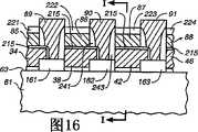
图16示出示出沿图3中的II-II截面、在成型图6A和6B所示第三单元阵列实施例期间出现的后续结构的剖视图;Figure 16 shows a cross-sectional view showing the subsequent structure occurring during the formation of the third cell array embodiment shown in Figures 6A and 6B along the II-II section in Figure 3;
图17A、17B和17C分别示出沿图3中的I-I截面、II-II截面和III-III截面、根据本发明第五特定实施例的存储单元的剖视图;17A, 17B and 17C show cross-sectional views of a memory cell according to a fifth specific embodiment of the present invention along the I-I cross-section, II-II cross-section and III-III cross-section in FIG. 3, respectively;
图18示出第五实施例的结构和操作过程;Fig. 18 shows the structure and operation process of the fifth embodiment;
图19是根据本发明第六特定实施例的存储单元阵列的平面图;以及19 is a plan view of a memory cell array according to a sixth specific embodiment of the present invention; and
图20是沿图19中的IV-IV的图19所示存储单元阵列的剖视图。FIG. 20 is a sectional view of the memory cell array shown in FIG. 19 taken along line IV-IV in FIG. 19 .
典型实施例的说明Description of Typical Embodiments
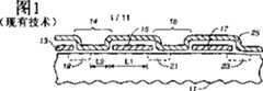
图1所示的剖视图示出典型分裂沟道现有技术存储单元和存储阵列,其中半导体衬底11具有分布在其表面上的二维阵列浮栅行和浮栅列。图1示出了沿行互相相邻的浮栅13、15和17。在浮栅之间存在间隔14和16。细长源漏扩散19、21和23在衬底上以进入图页的方向互相平行延伸。导电字线25在一行浮栅上并沿该行浮栅延伸。有些存储器对衬底擦除浮栅,而其它存储器在各行浮栅之间具有第三栅(未示出),其与至少各行中的一行浮栅电容耦合,以通过使电子通过隧道穿过它们之间的介质擦除该浮栅。为了使该图整洁所以未示出各栅之间的以及各栅与衬底之间的介质层,但是它们显然是存在的。The cross-sectional view shown in FIG. 1 shows a typical split-channel prior art memory cell and memory array in which a
这种存储单元的沟道被分裂为两段。一段L1由浮栅15的电压控制,而浮栅15的电压却受其字线25上的电压的影响,而另一段L2直接由字线25的电压控制。实际上,该单元由两个串联晶体管:浮栅晶体管(L1)和选择晶体管(L2)构成。字线25上的电压控制该电压所施加的每个单元的选择晶体管是接通还是断开,并因此控制这些单元的浮栅晶体管是否连接在单元的相邻源漏扩散之间,例如图中所示单元扩散19与21之间。The channel of this memory cell is split into two segments. One segment L1 is controlled by the voltage of the floating
图2示出图1所示单元和阵列的变换例。附加了在进入图页的方向是细长形的导引栅27、29和31。这些导引栅沿浮栅列延伸,而且在与它们电容耦合。它们使字线不与在该字线上通过的浮栅相连。通过与各单元沟道的L2段相连,字线上的电压仍对其行内各单元的选择晶体管进行控制,但是不再用于控制各浮栅的电压。这种阵列的导引栅也如此。导引栅上的电压选择用于进行编程或读的浮栅。然后,可以利用源极端注入进行编程,在编程期间,该方法可以采用降低的电流和/或电压。可以对衬底或字线擦除浮栅。FIG. 2 shows an alternative example of the cells and arrays shown in FIG. 1 . Added are
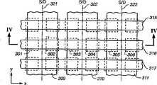
图3以平面图方式示出半导体衬底61表面63上的浮栅存储单元阵列的少量元件,作为以下各剖视图的基准结构。浮栅33至48以互相垂直的行(表示沿“x”方向延伸)和列(表示沿“y”方向延伸)的阵列方式排列。各浮栅的形状是长方形的,通常是正方形的,而且在每个x方向和y方向互相隔离开。源漏扩散51、53、55、57和59在y方向是细长形的,并在x方向互相隔离开,它们位于浮栅列之间。存储元件的此一般情况对于图4A至图7B所示的4种不同结构均是相同的。FIG. 3 shows a plan view of a small number of elements of the floating gate memory cell array on the
存储单元和存储阵列的第一特定实施例First specific embodiment of memory cell and memory array
在图4A和4B所示的垂直剖视图示出的该实施例中,交替扩散在衬底沟槽底部在x方向横跨衬底,而剩余扩散成型在衬底表面上。各沟槽在y方向是细长形的,并在x方向隔离开。例如,扩散53和57位于衬底61的各沟槽64和66的底部,而扩散55成型在衬底表面63上。字线67至70是细长形的,其长度在一行浮栅上、在横跨衬底的x方向延伸,而在y方向隔离开。字线包括向下延伸进入沟槽的选择栅,如图4A所示,对于字线69,在沟槽64和66内具有选择栅。沟槽壁与其内的选择栅之间的薄介质使选择栅与两个相对沟槽壁内的沟道部分之间实现电容耦合。因此,字线上的电压控制沿单元行的沟槽壁沟道部分L2的导通。由第一沉积多晶硅层成型浮栅,而由后续沉积的另一多晶硅层成型字线。In this embodiment, shown in the vertical cross-sectional view shown in Figures 4A and 4B, alternating diffusions are formed across the substrate in the x-direction at the bottom of substrate trenches, while the remaining diffusions are patterned on the substrate surface. The trenches are elongated in the y-direction and spaced apart in the x-direction. For example, diffusions 53 and 57 are located at the bottom of
单独沟槽的每个侧壁均是选择晶体管的沟道。例如,对于包括浮栅43的存储单元,沟道的L2部分沿着沟槽66的一个侧壁,而沟道的L1部分沿着衬底表面63。包括浮栅44的相邻存储单元将沟槽66的对面侧壁用作其选择栅沟道部分L2,而沟道部分L1沿着衬底表面。因此,各相邻存储单元在横跨衬底的x方向互为镜像。由于垂直成型各单元的选择晶体管沟道部分L1,所以在横跨衬底61的x方向可以降低阵列的尺寸。然而,该浮栅仍保持横跨衬底61的表面63。Each sidewall of a separate trench is a channel for a selection transistor. For example, for a memory cell including floating
作为擦除浮栅的机制,由其长度以x方向延伸的第三多晶硅层成型擦除栅71-73。各擦除栅在y方向隔离开,并位于各浮栅行之间。每个擦除栅最好通过隧道介质层与位于擦除栅一端上的行中的各浮栅实现电容耦合,而不与位于另一端上的行中的各浮栅实现电容耦合。作为一种选择,可以省略位于横跨衬底的x方向上的各交替擦除栅,而剩余擦除栅与位于两端上的各浮栅行相连。As a mechanism for erasing the floating gates, the erasing gates 71-73 are formed from a third polysilicon layer whose length extends in the x-direction. The erase gates are spaced apart in the y-direction and are located between rows of floating gates. Each erasing gate is preferably capacitively coupled to the floating gates in the row at one end of the erasing gate through the tunnel dielectric layer, but not capacitively coupled to the floating gates in the row at the other end of the erasing gate. As an option, the alternate erase gates located in the x-direction across the substrate can be omitted, with the remaining erase gates connected to rows of floating gates located at both ends.
在图4A和4B所示的第一实施例中,通过对衬底61擦除浮栅,不需要成型擦除栅。这是通过对要擦除的各单元的源极、漏极、衬底以及字线施加适当电压从而使其浮栅电压比衬底电压足够低实现的。然后,电子通过隧道穿过浮栅介质到达衬底。In the first embodiment shown in FIGS. 4A and 4B, by erasing the floating gate to the
存储单元和存储阵列的第二特定实施例Second specific embodiment of memory cell and memory array
图5A和5B所示的垂直剖视图示出其浮栅、沟槽以及扩散的结构与第一实施例的浮栅、沟槽以及扩散的结构相同,而由第二和第三多晶硅层成型的各栅不同的第二实施例。所成型的第二多晶硅层进入在y方向是细长形的、而在横跨衬底61的x方向隔离开的导引栅75至78内。每个导引栅横跨与其实现电容耦合的各浮栅列延伸,因此导引栅的部分电压与其下面的浮栅相连。The vertical cross-sectional views shown in Figures 5A and 5B show that the structure of the floating gate, trench and diffusion is the same as that of the first embodiment, but is formed by the second and third polysilicon layers. The second embodiment is different for each gate. The second polysilicon layer is patterned into
由第三多晶硅层成型字线79至82。从图5A可以看出,各选择晶体管栅从字线81向下延伸进入沟槽64和66。与第一实施例中相同,选择栅与在x方向互相相对的、沟槽的两侧实现电容耦合。可以利用位于字线与浮栅之间的较厚共聚介质,对字线擦除浮栅。作为一种选择,可以对衬底擦除该实施例的浮栅。如果对衬底进行擦除,则使浮栅与衬底之间的介质较薄,例如在100埃厚度范围内。Word lines 79 to 82 are formed from the third polysilicon layer. As can be seen in FIG. 5A , each select transistor gate extends down from
利用导引栅可以将第一实施例的各控制栅接通各选择晶体管并同时将要求电压连接到浮栅的各功能分开。可以单独对这些电压进行优化,而不对控制栅施加折衷电压。在进行编程和读期间,利用字线上的电压控制第二实施例的选择栅,同时将适当电压从导引栅连接到浮栅。另一个优点在于,可以利用低电压从其源极端编程单元。Using the steering gate allows the control gates of the first embodiment to switch on the select transistors while separating functions requiring voltage connections to the floating gates. These voltages can be optimized independently without applying a compromise voltage to the control gate. During programming and reading, the select gate of the second embodiment is controlled by the voltage on the word line, while the appropriate voltage is connected from the steering gate to the floating gate. Another advantage is that a cell can be programmed from its source terminal with a low voltage.
存储单元和存储阵列的第三特定实施例Third specific embodiment of memory cell and memory array
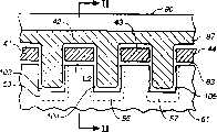
图6A和6B所示的垂直剖视图示出采用不同于第一和第二实施例的沟槽结构的单元阵列。在此第三实施例中,在每列浮栅之间设置沟槽。图6A所示的沟槽103、104和105的宽度完全是、或者几乎完全是包括各浮栅41至44的各相邻浮栅列之间的距离。在各沟槽103、104和105的底部以及一侧的上面成型源漏扩散53、55和57,该侧全部对着同一个方向。单元的选择栅沟道L2位于每个沟槽上、对着含有扩散的侧壁的侧壁上。浮栅41至44保留在衬底表面63上,并在x方向在位于其两侧之上的沟槽之间延伸。扩散的侧壁部分延伸到衬底表面63,而且表面63上的扩散分别被浮栅覆盖。源漏扩散具有扩大的截面,这样可以提高它们的电导率,并因此减少在y方向沿长度制造的接点的数量。Vertical sectional views shown in FIGS. 6A and 6B show cell arrays employing trench structures different from those of the first and second embodiments. In this third embodiment, trenches are provided between each column of floating gates. The width of the
延伸到沟槽内的选择栅是各字线85至88的一部分。从图6A中可以看出,字线87具有延伸到每个沟槽103、104以及105内的选择栅。它们与成型L2选择晶体管沟道部分的每个沟槽的一侧实现电容耦合以选择电流是否流过其各单元衬底沟道。以类似于第一实施例的方式,在各行之间设置擦除栅89至91,并使擦除栅89至91与至少一个相邻行实现电容耦合用于进行擦除,但是如果已经对衬底61擦除了浮栅,则省略擦除栅89至91。The select gates extending into the trenches are part of the respective wordlines 85-88. As can be seen in FIG. 6A ,
存储单元和存储阵列的第四特定实施例Fourth specific embodiment of memory cell and memory array
在图7A和7B示出的垂直取向剖视图所示的第四实施例中,沟槽结构、浮栅位置以及源漏扩散布局与上述第三实施例相同。对该实施例附加了在y方向是细长形的、而在x方向隔离开的导引栅93至96,导引栅93至96在各浮栅列上延伸并类似于上述第二实施例在它们与浮栅之间实现电容耦合。上述已经对采用导引栅的优点进行了讨论。在x方向是细长形的而在y方向隔离开的字线99至102包括向下延伸到沟槽内、并与位于含有扩散的侧壁对面的沟槽壁实现电容耦合的各选择栅,例如图7A所示字线101的各选择栅。与第二实施例相同,最好对字线擦除浮栅,但是也可以对衬底擦除浮栅。In the fourth embodiment shown in the vertical orientation cross-sectional view shown in FIGS. 7A and 7B , the trench structure, floating gate position, and source-drain diffusion layout are the same as those of the above-mentioned third embodiment. Added to this embodiment are
从图4A和5A中可以注意到,在观看x方向的剖视图时,第一实施例和第二实施例的各紧密相邻单元互为镜像。相反,第三实施例和第四实施例的各相邻单元在x方向不互为镜像,从图6A和7A中可以观察到。这四个实施例在y方向均不互为镜像。It can be noted from FIGS. 4A and 5A that the immediately adjacent units of the first embodiment and the second embodiment are mirror images of each other when viewing the cross-sectional view in the x direction. In contrast, adjacent cells of the third and fourth embodiments are not mirror images of each other in the x-direction, as can be observed from FIGS. 6A and 7A . None of these four embodiments are mirror images of each other in the y-direction.
采用存储单元和存储阵列的上述实施例的存储系统Storage system using the above-mentioned embodiments of the storage unit and the storage array
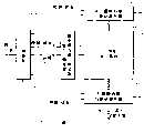
图8所示的方框图概括示出引入图5A、5B以及图7A、7B所示第二和第四实施例的存储系统例子。这些实施例均采用了沿浮栅列延伸的导引栅。在行和列的常规阵列111内排列根据第二和第四特定实施例的大量可单独寻址存储单元,当然也可以采用单元的其它物理排列。通过导线115,将在此设计的、沿单元阵列111的各列延伸的位线电连接到位线解码器与驱动器电路113。在此说明书中设计沿单元阵列111的各行延伸的字线通过导线117电连接到字线解码器与驱动器电路119。沿阵列111内的各存储单元的各列延伸的导引栅通过导线123电连接到导引栅解码器与驱动器电路121。利用Harari等人于2001年5月31日提交的标题为:“Steering Gate and Bit LineSegmentation in Non-Volatile Memories”的第09/871,333号未决专利申请描述的技术将导引栅和/或位线连接到相应解码器,在此引用该专利申请的全部内容供参考。每个解码器113、119以及121通过总线125从存储器控制器127接收存储单元地址。解码器与驱动电路还通过相应控制与状态信号线129、131以及133连接到控制器127。通过互连在解码器与驱动器电路113与121之间的总线122协调对导引栅和位线施加的电压。The block diagram shown in Fig. 8 schematically shows an example of a storage system incorporating the second and fourth embodiments shown in Figs. 5A, 5B and Figs. 7A, 7B. Both of these embodiments employ a steering gate extending along a column of floating gates. A large number of individually addressable memory cells according to the second and fourth particular embodiments are arranged in a
控制器127可以通过导线135连接到主机设备(未示出)。该主机可以是个人计算机、笔记本计算机、数码相机、声频播放器、各种其它手持电子设备等。通常在根据现有几个物理和电标准之一,例如,PCMCIA、CompactFlashTM协会、MMCTM协会等之一在卡内实现图8所示的存储系统。如果在卡格式中,导线135终止在卡上的连接器内,该卡的连接器与主机设备的互补连接器相连。许多卡的电接口符合ATA标准,其中对于主机,存储系统的作用就好象磁盘驱动器。还存在其它存储卡接口标准。作为卡格式的一种选择标准,将图8所示类型的存储系统永久嵌入主机设备内。
根据相应控制与状态线129、131和133上的控制信号,解码器与驱动器电路113、119以及121在通过总线125寻址的、阵列111的相应导线上产生适当电压,从而实现编程、读以及擦除功能。通过同一条控制与状态线129、131和133,阵列111将包括电压电平和其它阵列参数的任何状态信号送到控制器127。多个读出放大器137通过导线139从电路113接收电流电平或电压电平,指出阵列111内编址存储单元的状态,而且在进行读期间,通过导线141将关于这些状态的信息送到控制器127。为了能够并行读取大量存储单元的状态,通常使用大量读出放大器137。在进行读和编程期间,通常在某个时间通过电路119寻址一行单元,以访问电路113和121选择的编址行内的多个单元。在进行擦除期间,通常将许多行中每行上的所有单元作为块同时擦除。In response to control signals on respective control and
图9示出一个类似存储系统,不同之处在于存储单元阵列具有单独擦除栅,而不采用导引栅。这种阵列的例子是上述参考图4A、4B和6A、6B描述的第一和第三实施例。代替图8所示的导引栅解码器与驱动器电路121,而包括擦除栅解码器与驱动器电路143。通过导线145对为了进行同时擦除选择的各单元的擦除栅施加适当擦除电压。通过互连在解码器与驱动器电路113与143之间的总线147,协调对擦除栅和位线施加的电压。Figure 9 shows a similar memory system, except that the memory cell array has a separate erase gate instead of a steering gate. Examples of such arrays are the first and third embodiments described above with reference to Figures 4A, 4B and 6A, 6B. Instead of the pilot gate decoder and
在上述背景技术部分提及的专利以及转让给本发明受让人的SanDisk公司的其它专利中,对诸如图8和9所示的存储系统的存储系统的操作过程进行了披露。此外,2001年2月26日提交的第09/793,370号美国专利申请披露了一种数据编程方法,在此引用该专利申请供参考。The operation process of a storage system such as the storage system shown in FIGS. 8 and 9 is disclosed in the patents mentioned in the above background section and other patents of SanDisk Corporation assigned to the assignee of the present invention. Additionally, US Patent Application No. 09/793,370, filed February 26, 2001, which is incorporated herein by reference, discloses a data programming method.
可以对上述这4种单元和阵列实施例之任一进行调整以对衬底擦除浮栅,而不对擦除栅(图4A、4B和6A、6B所示的实施例)或字线(图5A、5B和7A、7B所示的实施例)擦除浮栅。在这些情况下,对衬底以及被同时擦除的存储单元的源极、漏极和导引栅施加适当电压。对于图4A、4B和6A、6B所示的情况,取消了擦除栅,因此使得各单元具有成型在各栅内的两层多晶硅层,而不是3层多晶硅层。Any of the four cell and array embodiments described above can be tuned to erase the floating gate to the substrate, but not the gate (the embodiments shown in FIGS. 4A, 4B and 6A, 6B) or the word line (Fig. 5A, 5B and 7A, 7B) erase the floating gate. In these cases, appropriate voltages are applied to the substrate and the sources, drains and steering gates of the memory cells being erased at the same time. For the cases shown in Figures 4A, 4B and 6A, 6B, the erase gate is eliminated, thus allowing each cell to have two layers of polysilicon formed in each gate instead of 3 layers of polysilicon.
实现存储单元和存储阵列的上述实施例的方法The method for implementing the above-mentioned embodiments of the storage unit and the storage array
图10至16所示的剖视图示出在实现上述图6A和6B所示存储单元和存储阵列第三实施例的过程中的顺序步骤。然而,根据如下说明显而易见,在实现上述第一、第二以及第四实施例过程中也包括在此具体描述的过程中的许多步骤。The cross-sectional views shown in FIGS. 10 to 16 illustrate sequential steps in the process of implementing the third embodiment of the memory cell and memory array shown in FIGS. 6A and 6B described above. However, it is apparent from the following description that many steps in the process specifically described here are also included in the process of implementing the above-mentioned first, second and fourth embodiments.
图10A和10B示出几个初始处理步骤的处理结果。通过在衬底61的表面63上沉积一层约2000埃厚度的氧化物成型场氧化物条161至163。然后,利用光致抗蚀剂掩模将该层蚀刻为条161至163,它们具有沿x方向横跨衬底延伸的长度,并在y方向将它们隔离开。栅氧化物层165至168是在场氧化物条161-163之间的衬底表面63上形成的,它们的厚度约为150埃。下一步是在场氧化物和栅氧化物上沉积约2000埃厚度的第一多晶硅层171。然后,由该多晶硅层上成型阵列的浮栅。由于其上沉积多晶硅层的底层表面不规则,所以为了获得较平滑表面,所沉积的多晶硅的厚度大于对浮栅需要的厚度,然后,将该表面氧化到希望过量多晶硅材料被去除的深度,从而使多晶硅层171具有要求厚度和较平坦上表面。10A and 10B illustrate the processing results of several initial processing steps. Field oxide strips 161 to 163 are formed by depositing a layer of oxide on
在对该多晶硅层实现平面化后的下一个步骤是在多晶硅层171的上部形成(grow)约200埃厚的氧化物层173。此步骤之后是在氧化物层171上沉积约1500埃厚的氮化物层175。接着,在该氮化物层上沉积约500埃厚的氧化物层177。最后形成被称为“ONO”结构的三层介质。之后,氮化物层用作结束对表面进行化学-机械平面化(“CMP”)的阻挡层(stop)。The next step after planarizing the polysilicon layer is to grow an
下一步是在ONO结构上沉积这样厚的多晶硅保护层,即在对衬底表面63蚀刻沟槽时的后续步骤被去除的厚度。如图11A和11B所示,将两层多晶硅层、中间ONO介质以及场氧化物条向下蚀刻通过掩模(未示出)到达衬底表面以成型第一多晶硅层171条181至183,并清除这些条之间的衬底。条181至183具有沿y方向横跨衬底表面63延伸的长度,而且它们在x方向被隔离开。上部多晶硅层同样被分割为条185至187。The next step is to deposit a protective polysilicon layer on the ONO structure so thick that it will be removed by subsequent steps when etching the trenches to the
然后,图11A和11B所示的结果结构用作掩模以在硅衬底61上蚀刻沟槽191至194,如图12A和12B所示。在成型衬底沟槽191至194的同时去除上部多晶硅层(条185至187),使ONO介质结构保留在适当位置,如图12A和12B所示。接着,最好以两个步骤实现源漏植入(implantation)。第一源极位置197使离子进入垂直于衬底表面63的通路以在沟槽底部形成掺杂区,例如植入沟槽192底部的区域199。ONO和第一多晶硅层条形成植入掩模。第二源极位置201与衬底表面63成θ角以沿每个沟槽的一侧形成掺杂区,例如沿沟槽192的一个侧壁的区域203。所选择的角θ足以从其底部到衬底表面63暴露整个沟槽侧壁。在后续退火步骤中离子扩散的结果使离子进入连续区205(图13A),该连续区205从衬底表面开始沿一个沟槽侧壁延伸到沟槽底部并沿沟槽底部到对面侧壁。对面侧壁未被植入,因为它构成成品器件存储单元衬底沟道的选择晶体管部分。Then, the resulting structure shown in FIGS. 11A and 11B is used as a mask to etch
如图13A、13B和13C所示,下一步是在整个阵列上沉积约5000埃的非常厚的氧化物层。这样可以完全填充所有沟槽,而且在该结构上延伸,如虚线轮廓所示。然后,利用CMP处理过程去除过量氧化物,向下到作为CMP处理的阻挡层的氮化物层175。下一步是成型细长形条掩模(未示出),其具有沿x方向横跨平面化表面延伸的长度,其间隔确定待清除的、沟槽内的氧化物。将位于要成型存储单元位置的,即位于在之后设置字线和选择栅位置的沟槽氧化物去除,而保留衬底上y方向各单元之间沟槽内的氧化物。该保留氧化物在各行单元之间提供介质隔离。图13C示出其最佳情况,其中所示的氧化物段207至210与被去除了氧化物的开口位置211至213沿沟槽193的长度交替出现。As shown in Figures 13A, 13B and 13C, the next step is to deposit a very thick oxide layer of about 5000 Angstroms over the entire array. This completely fills all trenches and extends over the structure, as shown in dashed outline. The excess oxide is then removed using a CMP process, down to the
参考图14A、14B和14C,下一步是在多晶硅条181至183上以及衬底沟槽191至194的开口表面之上形成70至100埃的氧化物层215。然后,在阵列上沉积另一个多晶硅层以延伸到沟槽的开口区域内。然后,在该多晶硅层上沉积约1500埃的氧化物层。然后,使该组合形成图形以去除多晶硅条和各行存储单元之间的底层氧化物,保留具有在衬底表面63上沿x方向长度的并且在衬底表面63上的y方向被隔离开的细长形字线85至88。然后,使氧化物条221至224保留在相应字线85至88上。Referring to FIGS. 14A , 14B and 14C, the next step is to form an
然后,将第一多晶硅条分离为单个浮栅,如图15A和15B所示。为此,对在x方向是细长形的条231至233成型光致抗蚀剂掩模。以这样的方式在y方向定位这些条,以致每个条均在相应字线的一个边缘上延伸,以在它与相连字线的对面边缘之间成型窄掩模开口。然后,通过这些掩模开口蚀刻第一多晶硅条以例如由多晶硅条171成型浮栅34、38、42和46,如图15B所示。Then, the first polysilicon strip is separated into individual floating gates, as shown in Figures 15A and 15B. For this purpose, a photoresist mask is patterned for the strips 231 to 233 which are elongated in the x-direction. The strips are positioned in the y-direction in such a way that each strip extends over one edge of the respective wordline to form a narrow mask opening between it and the opposite edge of the associated wordline. The first polysilicon strips are then etched through these mask openings to form floating
下一个顺序步骤是清除光致抗蚀剂掩模,并沿暴露多晶硅壁成型介质隔离层(spacer),如图16所示。在去除光致抗蚀剂掩模条231至233后,在图15A和15B所示的结构上沉积厚氧化物层,然后,利用各向异性蚀刻过程去除氧化物,从而保留沿着垂直壁的各侧壁隔离层,例如图16所示的隔离层241和243。这样可以暴露浮栅边缘。在这些边缘上形成约100埃后的层,图16所示的层245是这些层之一。然后,在该阵列上沉积另一个多晶硅层,并使该多晶硅层形成图形以保留擦除栅89至91。薄氧化物层245允许对擦除栅90擦除浮栅38,而隔离层241和243将擦除栅90与相邻控制栅86和87隔离开,并与浮栅42隔离开,因此不与它们中之任一发生电容耦合。The next sequential step is to remove the photoresist mask and form a dielectric spacer along the exposed polysilicon walls, as shown in FIG. 16 . After removing the photoresist mask strips 231 to 233, a thick oxide layer is deposited on the structure shown in FIGS. Each sidewall isolation layer is, for example, the isolation layers 241 and 243 shown in FIG. 16 . This exposes the floating gate edges. Layers after about 100 angstroms are formed on these edges, layer 245 shown in FIG. 16 being one of these layers. Another layer of polysilicon is then deposited over the array and patterned to retain erase gates 89-91. Thin oxide layer 245 allows
对形成图6A和6B所示第三实施例的单元阵列的上述特定处理细节进行调整以形成图7A和7B所示第四实施例的单元阵列。主要差别是在成型字线99至102之前成型导引栅93至96,当然就省略了擦除栅89至91。The specific processing details described above for forming the cell array of the third embodiment shown in FIGS. 6A and 6B are adjusted to form the cell array of the fourth embodiment shown in FIGS. 7A and 7B . The main difference is that the
形成图4A至5B所示第一和第二实施例的过程与形成图6A至7B所示第三和第四实施例的过程的不同之处在于,仅在浮栅之间每隔一个间隔的间隔内,在衬底上成型沟槽。因此,在进行衬底蚀刻步骤之前,成型临时覆盖第一多晶硅层各条之间的交替间隔的掩模。此外,省略成角度离子植入201(参考图12A),因为在这些实施例中不要求沿沟槽侧壁提供扩散。The process of forming the first and second embodiments shown in FIGS. 4A to 5B differs from the process of forming the third and fourth embodiments shown in FIGS. 6A to 7B in that only every other spacer between the floating gates Within the space, trenches are formed on the substrate. Therefore, before performing the substrate etching step, a mask is formed temporarily covering the alternating spaces between the strips of the first polysilicon layer. Furthermore, angled ion implantation 201 (see FIG. 12A ) is omitted because in these embodiments it is not required to provide diffusion along the trench sidewalls.
存储单元和存储阵列的第五特定实施例Fifth specific embodiment of memory cell and memory array
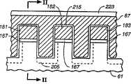
图17A、17B和17C所示的单元结构采用了选择栅,并使源漏扩散位于衬底表面上的沟槽之外。对沟槽侧壁作用的结果是,沟槽增加了选择晶体管沟道的长度。这样可以使单元的表面积随着处理技术的进步成正比缩小,同时对选择晶体管沟道长度保留某种程度的独立控制,以降低缩小单元内选择晶体管击穿的概率。图17A、17B和17C所示的存储单元没有必要对沟槽的源漏区域成型离子植入,而且不需要使浮栅位于沟槽内。The cell structures shown in Figures 17A, 17B and 17C employ select gates and have the source and drain diffusions located outside the trenches on the substrate surface. As a result of acting on the sidewalls of the trench, the trench increases the length of the select transistor channel. This allows the surface area of the cell to shrink proportionally with the progress of processing technology, while retaining some degree of independent control over the channel length of the select transistor to reduce the probability of breakdown of the select transistor in the shrink cell. The memory cells shown in FIGS. 17A, 17B and 17C do not need to form ion implantation in the source and drain regions of the trench, and do not need to have the floating gate located in the trench.
现在说明此存储单元的例子,剖视图17A、17B和17C分别是沿图3所示平面图的截面I-I、II-II和III-III的剖视图。衬底上的沟槽,例如沟槽251和253在y方向是细长形的,而在x方向被隔离开。在所示的、在y方向是细长形的而在x方向被隔离开的掺杂多晶硅导引栅255、257和259与相应底层浮栅42、43和44之间具有共聚介质。在此描述的使用沟槽的方法还可以应用于不采用导引栅的单元阵列。在x方向是细长形的而在y方向被隔离开的掺杂多晶硅字线261、263、265和267在各行浮栅和中间导引栅上延伸,而且在它们之间具有适当共聚介质层。Now explaining an example of this memory cell,
每个字线还延伸到其行内的每个存储单元的沟槽内以成型选择晶体管浮栅,例如作为字线265的一部分的栅269和271。在每个这种栅与它所在的衬底沟槽的内侧之间设置适当栅介质层。字线上的电压将该电压施加到沿该字线的所有选择晶体管浮栅上。该电压通过栅介质连接到作为选择晶体管的沟道的沟槽的对面部分、侧壁和底部上。在运行该存储系统期间选择该电压,以根据为了进行编程或读是否询问字线的存储单元行来接通或断开字线的单元选择晶体管。利用使电子通过隧道穿过浮栅34、38、42以及46与字线之间的介质层,这种存储阵列可以对字线擦除其单元,或者通过使电子通过隧道穿过浮栅与衬底之间的栅介质对衬底擦除其单元。在图8所示的系统中可以采用根据图17A、17B和17C的存储单元阵列。如果不采用导引栅而且附加擦除栅,则在图9所示的系统内采用这种阵列。Each wordline also extends into the trenches of each memory cell within its row to form select transistor floating gates, such as
最好使选择栅所延伸的衬底沟槽在y方向连续,并最好将氧化硅或某种其它适当介质填充到位于选择晶体管栅之间的这些沟槽内。对于沟槽253,图17C示出这种情况,其中示于选择晶体管栅之间、具有虚线阴影的区域表示该氧化物。作为一种选择,还可以成型连续沟槽,在衬底上成型在平面图中是正方形的凹槽(recess)以容纳选择栅和中间栅介质。Preferably, the substrate trenches from which the select gates extend are continuous in the y-direction, and silicon oxide or some other suitable dielectric is preferably filled into these trenches between the gates of the select transistors. For
为了更好地说明器操作过程,图18示出部分存储单元的放大图。与上述相同,相邻源漏扩散55与57之间的单元沟道的L1部分位于沿在单元浮栅43之下的衬底61的表面63、并与扩散57相邻。然而,选择晶体管栅部分L2从L1沟道部分沿衬底沟槽251的侧壁和底部延伸到另一个扩散55。位于沟槽内的栅(图18中未示出)是沿长度L1衬底的侧壁和底部通过栅介质层与衬底相连的场。当然,对于选择晶体管沟道部分沿着衬底表面,而不采用沟槽251的情况,该长度比直接通路L1’的长度长得多。在该特定例子中,使沟槽的深度在500埃至3000埃之间,对于大多数情况,适于具有约2000埃的深度。每个沟槽开口的尺寸L1’通常可以是处理过程中使用的最小特征图形尺寸的尺寸。In order to better explain the operation process of the device, FIG. 18 shows an enlarged view of a part of the storage unit. As above, the L1 portion of the cell channel between adjacent source-
采用这种沟槽的一个优点是可以提高编程效率。如箭头275所示,在利用源极端注入进行编程期间,电子沿着选择晶体管沟道内的沟槽251的内侧壁加速向上。与在蚀刻沟槽251期间,浮栅边缘用作部分掩模的情况相同,在浮栅紧靠在沟槽251边上时,这些电子在与浮栅43的边缘直接相交的通路内传播。预期电子注入浮栅的效率更高,因为这些电子以其动量方向注入浮栅。在电子在沿与浮栅直接相交的沟槽侧壁的通路内以高能量运动时,此优点还适于在此描述的其它实施例。One advantage of using such trenches is that programming efficiency can be improved. As indicated by arrow 275, during programming using source terminal injection, electrons are accelerated upward along the inner sidewall of
形成图17A至17C所示的沟槽结构的一种方式是在源漏区域的衬底内注入离子,然后成型第一多晶硅层条,而无需与植入实现自对准。然后,沿多晶硅条的边缘在条上施加掩模材料,该多晶硅条同样对着x方向但是在这些掩模条与相邻多晶硅条之间保留间隔。这些间隔确定沟槽,然后通过该间隔将该沟槽蚀刻到衬底内。作为一种选择,可以沿多晶硅条的边缘成型介质隔离层,而交替去除沿着一个方向的边缘的隔离层。这样可以保留剩余隔离层与通过其蚀刻沟槽的相邻多晶硅条边缘之间的间隔。从图17A至C中可以看出,在每个剖视图中,该阵列结构的存储单元具有常规非镜像图形。One way to form the trench structure shown in FIGS. 17A to 17C is to implant ions into the substrate in the source and drain regions, and then form the first polysilicon layer strips without self-alignment with the implantation. A masking material is then applied over the strips along their edges, also facing the x-direction but leaving a space between these masked strips and adjacent polysilicon strips. These spaces define trenches, which are then etched into the substrate through the spaces. As an option, dielectric spacers can be formed along the edges of the polysilicon strips, while the spacers along the edges in one direction are alternately removed. This preserves the spacing between the remaining spacer and the edge of the adjacent polysilicon strip through which the trench is etched. As can be seen from FIGS. 17A to C, in each cross-sectional view, the memory cells of the array structure have a conventional non-mirror pattern.
存储单元和存储阵列的第六特定实施例Sixth specific embodiment of memory cell and memory array
图17A至18所示实施例的变换例将其选择晶体管栅沟槽设置在在上述背景技术中参考在此引用的特定专利和专利申请描述的双存储元件单元(Dual Storage Element Cell)的两个浮栅之间。对于为了描述双存储元件单元引用的文件内描述的这种单元的一种特定形式,在此说明了选择晶体管栅的用法。图19示出这种单元阵列的部分平面图,而图20示出沿其IV-IV(沿x方向)截面的、该阵列的剖视图,它示出选择晶体管栅沟槽的位置。通过参考所引用的专利和专利申请,可以得知这种双存储元件单元的其它细节以及构造它们的方法。The modification of the embodiment shown in FIGS. 17A to 18 sets its selection transistor gate trenches in two of the dual storage element cells (Dual Storage Element Cell) described in the above-mentioned background art with reference to specific patents and patent applications cited here. between floating gates. For a particular version of such a cell described in the documents cited for describing a dual storage element cell, the use of a select transistor gate is illustrated here. Figure 19 shows a partial plan view of such a cell array, while Figure 20 shows a cross-sectional view of the array along its IV-IV (in the x direction) section, showing the location of the select transistor gate trenches. Additional details of such dual memory element cells and methods of constructing them can be found by reference to the cited patents and patent applications.
参考图19,在虚线轮廓内示出部分二维阵列浮栅。示出两个存储单元的图20所示的剖视图是在x方向通过一行浮栅301至306的剖视图。导引栅309、310和311在y方向是细长形的,其在x方向的宽度是两个相邻浮栅列之间的距离。作为一种选择,每列浮栅可以具有单独导引栅。字线315、316和317在x方向是细长形的,并在y方向位于各列浮栅之上。在半导体衬底327上形成源漏扩散321、322和323,它们在y方向是细长形的,其长度横跨大量行,而且在x方向被隔离开。衬底327上的沟槽331和332在y方向是细长形的而在x方向被隔离开,而且诸如作为字线316的一部分的栅335和336的选择晶体管栅位于其内。在所示元件之间的间隔内成型常规栅和共聚介质。Referring to FIG. 19, a portion of a two-dimensional array of floating gates is shown within dashed outline. The cross-sectional view shown in FIG. 20 showing two memory cells is a cross-sectional view through a row of floating
一个存储单元包括源漏(位线)扩散321和322,与这两个扩散相邻的两个浮栅302和303位于源漏扩散321与322之间。位于这两个浮栅之间的是衬底沟槽331和选择晶体管栅335。沟槽的侧壁和底部共同构成选择晶体管沟道的长度(L2)。扩散321与沟槽331之间的衬底区域是包括浮栅302的左存储晶体管的沟道长度(L1)。同样,扩散322与沟槽331之间的衬底区域是包括浮栅303的右存储晶体管的沟道长度(L1)。沟槽331以与上述参考图17A至18说明的同样方式工作,利用沟槽侧壁增加选择晶体管沟道的长度并提高编程效率。以同样方式构造阵列的其它存储单元,包括扩散322与323之间的部分。A memory cell includes source-drain (bit line) diffusions 321 and 322 , and two floating
通过利用将第一多晶硅层在x方向分离为单独浮栅所使用的相同的掩模蚀刻沟槽,可以与相邻浮栅对准成型衬底沟槽。在一种方式中,利用在其上表面上成型了保护材料(例如氧化物)层的导引栅成型此掩模。以同样图形继续蚀刻通过第一多晶硅层进入衬底327,但是对衬底使用的蚀刻剂与对浮栅多晶硅层使用的蚀刻剂不同。蚀刻沟槽后,在沟槽壁和底部表面上的暴露硅衬底表面上以及在多晶硅浮栅和导引栅的暴露侧面上成型薄介质层。可以通过在这些衬底上形成和/或沉积约200埃厚的二氧化硅,可以成型图20所示的围绕选择晶体管栅335和336的该栅介质。然后,最好在衬底上沉积第三掺杂多晶硅层以延伸到浮栅与导引栅之间的间隔内,此后,将该多晶硅层分离为所示字线。之后,在阵列上沉积诸如氧化物的厚介质以填充位于各行之间的选择晶体管栅沟槽从而将它们隔离开。By etching the trenches using the same mask used to separate the first polysilicon layer into individual floating gates in the x-direction, substrate trenches can be formed in alignment with adjacent floating gates. In one approach, the mask is patterned using a guide gate with a layer of protective material (eg, oxide) patterned on its upper surface. The etch continues through the first polysilicon layer into the substrate 327 in the same pattern, but with a different etchant for the substrate than for the floating gate polysilicon layer. After etching the trench, a thin dielectric layer is formed on the exposed silicon substrate surface on the trench wall and bottom surfaces and on the exposed sides of the polysilicon floating gate and steering gate. The gate dielectric surrounding select transistor gates 335 and 336 shown in FIG. 20 can be patterned by forming and/or depositing about 200 Angstroms thick silicon dioxide on these substrates. A third layer of doped polysilicon is then preferably deposited on the substrate to extend into the space between the floating gate and the steering gate, after which this layer of polysilicon is separated into the wordlines as shown. Afterwards, a thick dielectric such as oxide is deposited over the array to fill the select transistor gate trenches between the rows to separate them.
与图17A至18所示的存储单元相同,在图19和20所示的存储单元配置中,不是在衬底槽331和332的底部和侧面上,而是在衬底表面上成型源漏区域。这就是第五和第六实施例与第一至第四实施例的区别。然而,为了调节选择晶体管沟道的界限,选择晶体管沟道可以具有沿沟槽的侧面和底部植入的离子,与在沿衬底表面设置选择晶体管沟道时所进行的操作相同。As with the memory cell shown in Figures 17A to 18, in the memory cell configuration shown in Figures 19 and 20, instead of the bottom and sides of the substrate grooves 331 and 332, the source and drain regions are formed on the substrate surface . This is the difference between the fifth and sixth embodiments and the first to fourth embodiments. However, in order to adjust the boundaries of the select transistor channel, the select transistor channel may have ions implanted along the sides and bottom of the trench, as is done when the select transistor channel is provided along the substrate surface.
交替存储元件alternate storage element
根据将导电浮栅用作电荷存储元件的单元的类型,对上述发明内容和闪速EEPROM存储单元的特定例子进行了说明。然而,上述说明的许多单元结构和处理过程还可以应用于将电荷陷获(trapping)介质用作存储元件代替浮栅的存储单元。例如,可以利用该介质代替图4A-4B、5A-5B、6A-6B、7A-7B、17A-C以及20所示实施例的浮栅,然后将该介质插在导引栅与衬底之间。尽管可以将该介质分离为与浮栅具有同样大小、与浮栅位于同样位置的单独元件,但是通常不必这样做,因为这种介质在局部陷获电荷。除了选择晶体管占据的区域外,该电荷陷获介质可以在整个阵列上延伸。一种特定配置是在在y方向横跨大量单元行连续延伸的条内成型该介质,但是它们分别具有在x方向包含在相邻选择晶体管之间的宽度。在将介质之上的共聚层分离为细长形条的过程中,可以去除该介质的其它区域,而不会产生负面影响,但是不必这样做。位于每个单元内、插在单元沟道内的导电栅与衬底之间的部分介质是用于该单元的电荷存储元件。The foregoing summary and specific examples of flash EEPROM memory cells are described in terms of the type of cell that uses a conductive floating gate as the charge storage element. However, many of the cell structures and processes described above can also be applied to memory cells that use charge trapping media as storage elements instead of floating gates. For example, the dielectric can be used instead of the floating gate of the embodiments shown in FIGS. between. Although it is possible to separate the dielectric into a separate element of the same size and location as the floating gate, this is generally not necessary because the dielectric traps charge locally. This charge-trapping medium can extend across the entire array except for the area occupied by the select transistors. One particular configuration is to form the dielectric in strips extending continuously across a large number of cell rows in the y-direction, but each having a width in the x-direction contained between adjacent select transistors. During the separation of the co-polymeric layer above the media into elongated strips, other regions of the media can be removed without adverse effect, but need not be done. The portion of the dielectric within each cell between the conductive gate interposed in the cell's channel and the substrate is the charge storage element for that cell.
在以下技术论文和专利中对介质存储元件存储单元做了总体说明,在此引用这些论文和专利的全部内容供参考:Chan等人的“ATrue Single-Transistor Oxide-Nitride-Oxide EEPROM Device”,IEEEElectron Device Letters,Vol.EDL-8,No.3,March 1987,pp.93-95;Nozaki等人的“A1-Mb EEPROM with MONOS Memory Cell forSemiconductor Disk Application”IEEE Journal of Solid State Circuits,Vol.26,No.4,April 1991,pp.497-501;Eitan等人的“NROM:ANovel Localized Trapping,2-Bit Nonvolatile Memory Cell”IEEEElectron Device Letters,Vol.21,No.11,November 2000,pp.543-545,以及第5,851,881号美国专利。A general description of media storage element memory cells is given in the following technical paper and patent, which are incorporated herein by reference in their entirety: "ATrue Single-Transistor Oxide-Nitride-Oxide EEPROM Device" by Chan et al., IEEE Electron Device Letters, Vol.EDL-8, No.3, March 1987, pp.93-95; "A1-Mb EEPROM with MONOS Memory Cell for Semiconductor Disk Application" by Nozaki et al., IEEE Journal of Solid State Circuits, Vol.26, No.4, April 1991, pp.497-501; Eitan et al. "NROM: ANovel Localized Trapping, 2-Bit Nonvolatile Memory Cell" IEEE Electron Device Letters, Vol.21, No.11, November 2000, pp.543- 545, and U.S. Patent No. 5,851,881.
可以采用的特定电荷陷获介质材料和配置有三种。一种是双层介质,它具有形成在衬底上的氧化物层和沉积在其上的氮化硅层(“ON”)。另一种是三层结构,它增加了形成和/或沉积在氮化硅层上的另一个氧化硅层(“ONO”)。第三种结构是在栅与半导体衬底表面之间插入一层富硅二氧化硅。在以下两篇论文中对后一种材料进行了说明,在此引用其全部内容供参考:Dimaria等人的“Electrically-alterable read-only-memory using Si-rich SIO2 injectorsand a floatin polycrystalline silicon storage layer,”J.Appl.Phys.52(7),July 1981,pp.4825-4842;Hori等人的“A MOSFET withSi-implanted Gate-SiO2 Insulator for Nonvolatile MemoryApplications,”IEDM 92,April 1992,pp.469-472.There are three specific charge-trapping dielectric materials and configurations that can be used. One is a dual-layer dielectric that has an oxide layer formed on a substrate and a silicon nitride layer ("ON") deposited thereon. Another is a three-layer structure that adds another silicon oxide layer ("ONO") formed and/or deposited on top of the silicon nitride layer. The third structure is to insert a layer of silicon-rich silicon dioxide between the gate and the surface of the semiconductor substrate. The latter material is described in the following two papers, the entire contents of which are hereby incorporated by reference: Dimaria et al., "Electrically-alterable read-only-memory using Si-rich SIO2 injectors and a floating polycrystalline silicon storage layer ,” J.Appl.Phys.52(7), July 1981, pp.4825-4842; Hori et al., “A MOSFET with Si-implanted Gate-SiO2 Insulator for Nonvolatile Memory Applications,” IEDM 92, April 1992, pp.469 -472.
综述review
尽管根据本发明的特定例子,对本发明的各方面进行了说明,但是,显然,本发明应该受所附权利要求所述全部范围的保护。While various aspects of the invention have been described in terms of particular examples thereof, it should be evident that the invention should be protected to the full extent set forth in the appended claims.
Claims (35)
Translated fromChineseApplications Claiming Priority (4)
| Application Number | Priority Date | Filing Date | Title |
|---|---|---|---|
| US09/860,704US6894343B2 (en) | 2001-05-18 | 2001-05-18 | Floating gate memory cells utilizing substrate trenches to scale down their size |
| US09/860,704 | 2001-05-18 | ||
| US09/925,134US6936887B2 (en) | 2001-05-18 | 2001-08-08 | Non-volatile memory cells utilizing substrate trenches |
| US09/925,134 | 2001-08-08 |
Publications (2)
| Publication Number | Publication Date |
|---|---|
| CN1484861Atrue CN1484861A (en) | 2004-03-24 |
| CN1269217C CN1269217C (en) | 2006-08-09 |
Family
ID=27127584
Family Applications (1)
| Application Number | Title | Priority Date | Filing Date |
|---|---|---|---|
| CNB02802141XAExpired - Fee RelatedCN1269217C (en) | 2001-05-18 | 2002-05-08 | Non-volatile memory cells using substrate trenches |
Country Status (8)
| Country | Link |
|---|---|
| US (3) | US6936887B2 (en) |
| EP (1) | EP1388173A2 (en) |
| JP (1) | JP2005506685A (en) |
| KR (1) | KR20030014761A (en) |
| CN (1) | CN1269217C (en) |
| AU (1) | AU2002305467A1 (en) |
| TW (1) | TW550825B (en) |
| WO (1) | WO2002095829A2 (en) |
Cited By (1)
| Publication number | Priority date | Publication date | Assignee | Title |
|---|---|---|---|---|
| CN110277393A (en)* | 2019-06-19 | 2019-09-24 | 上海华力微电子有限公司 | Flash memory and manufacturing method thereof |
Families Citing this family (82)
| Publication number | Priority date | Publication date | Assignee | Title |
|---|---|---|---|---|
| US6936887B2 (en)* | 2001-05-18 | 2005-08-30 | Sandisk Corporation | Non-volatile memory cells utilizing substrate trenches |
| US6897522B2 (en) | 2001-10-31 | 2005-05-24 | Sandisk Corporation | Multi-state non-volatile integrated circuit memory systems that employ dielectric storage elements |
| US6925007B2 (en)* | 2001-10-31 | 2005-08-02 | Sandisk Corporation | Multi-state non-volatile integrated circuit memory systems that employ dielectric storage elements |
| US6542407B1 (en) | 2002-01-18 | 2003-04-01 | Sandisk Corporation | Techniques of recovering data from memory cells affected by field coupling with adjacent memory cells |
| US6888755B2 (en)* | 2002-10-28 | 2005-05-03 | Sandisk Corporation | Flash memory cell arrays having dual control gates per memory cell charge storage element |
| US6864519B2 (en)* | 2002-11-26 | 2005-03-08 | Taiwan Semiconductor Manufacturing Co., Ltd. | CMOS SRAM cell configured using multiple-gate transistors |
| US6894339B2 (en)* | 2003-01-02 | 2005-05-17 | Actrans System Inc. | Flash memory with trench select gate and fabrication process |
| US7001814B1 (en)* | 2003-05-16 | 2006-02-21 | Advanced Micro Devices, Inc. | Laser thermal annealing methods for flash memory devices |
| US7759719B2 (en)* | 2004-07-01 | 2010-07-20 | Chih-Hsin Wang | Electrically alterable memory cell |
| US7550800B2 (en)* | 2003-06-06 | 2009-06-23 | Chih-Hsin Wang | Method and apparatus transporting charges in semiconductor device and semiconductor memory device |
| US7049652B2 (en)* | 2003-12-10 | 2006-05-23 | Sandisk Corporation | Pillar cell flash memory technology |
| US20050251617A1 (en)* | 2004-05-07 | 2005-11-10 | Sinclair Alan W | Hybrid non-volatile memory system |
| KR100593599B1 (en)* | 2003-12-30 | 2006-06-28 | 동부일렉트로닉스 주식회사 | Manufacturing Method of Semiconductor Device |
| JP4509653B2 (en)* | 2004-05-28 | 2010-07-21 | 株式会社東芝 | Method for manufacturing nonvolatile semiconductor memory device |
| US20080203464A1 (en)* | 2004-07-01 | 2008-08-28 | Chih-Hsin Wang | Electrically alterable non-volatile memory and array |
| US7518179B2 (en) | 2004-10-08 | 2009-04-14 | Freescale Semiconductor, Inc. | Virtual ground memory array and method therefor |
| US7381615B2 (en)* | 2004-11-23 | 2008-06-03 | Sandisk Corporation | Methods for self-aligned trench filling with grown dielectric for high coupling ratio in semiconductor devices |
| US7416956B2 (en)* | 2004-11-23 | 2008-08-26 | Sandisk Corporation | Self-aligned trench filling for narrow gap isolation regions |
| US7217968B2 (en)* | 2004-12-15 | 2007-05-15 | International Business Machines Corporation | Recessed gate for an image sensor |
| KR100620223B1 (en)* | 2004-12-31 | 2006-09-08 | 동부일렉트로닉스 주식회사 | Manufacturing method of split gate flash Y pyrom |
| TWI270199B (en)* | 2005-01-31 | 2007-01-01 | Powerchip Semiconductor Corp | Non-volatile memory and manufacturing method and operating method thereof |
| TWI257150B (en)* | 2005-02-03 | 2006-06-21 | Powerchip Semiconductor Corp | Non-volatile memory and fabricating method and operating method thereof |
| TWI246748B (en)* | 2005-02-03 | 2006-01-01 | Powerchip Semiconductor Corp | Non-volatile memory and fabricating method and operating method thereof |
| US7365382B2 (en)* | 2005-02-28 | 2008-04-29 | Infineon Technologies Ag | Semiconductor memory having charge trapping memory cells and fabrication method thereof |
| US7411244B2 (en) | 2005-06-28 | 2008-08-12 | Chih-Hsin Wang | Low power electrically alterable nonvolatile memory cells and arrays |
| KR100678478B1 (en)* | 2005-06-29 | 2007-02-02 | 삼성전자주식회사 | NAND type nonvolatile memory device and manufacturing method thereof |
| US7759726B2 (en)* | 2005-07-12 | 2010-07-20 | Macronix International Co., Ltd. | Non-volatile memory device, non-volatile memory cell thereof and method of fabricating the same |
| US7642594B2 (en)* | 2005-07-25 | 2010-01-05 | Freescale Semiconductor, Inc | Electronic device including gate lines, bit lines, or a combination thereof |
| US7250340B2 (en)* | 2005-07-25 | 2007-07-31 | Freescale Semiconductor, Inc. | Method of fabricating programmable structure including discontinuous storage elements and spacer control gates in a trench |
| US7582929B2 (en)* | 2005-07-25 | 2009-09-01 | Freescale Semiconductor, Inc | Electronic device including discontinuous storage elements |
| US7226840B2 (en)* | 2005-07-25 | 2007-06-05 | Freescale Semiconductor, Inc. | Process for forming an electronic device including discontinuous storage elements |
| US7394686B2 (en)* | 2005-07-25 | 2008-07-01 | Freescale Semiconductor, Inc. | Programmable structure including discontinuous storage elements and spacer control gates in a trench |
| US7205608B2 (en)* | 2005-07-25 | 2007-04-17 | Freescale Semiconductor, Inc. | Electronic device including discontinuous storage elements |
| US7262997B2 (en)* | 2005-07-25 | 2007-08-28 | Freescale Semiconductor, Inc. | Process for operating an electronic device including a memory array and conductive lines |
| US7314798B2 (en)* | 2005-07-25 | 2008-01-01 | Freescale Semiconductor, Inc. | Method of fabricating a nonvolatile storage array with continuous control gate employing hot carrier injection programming |
| US7619270B2 (en)* | 2005-07-25 | 2009-11-17 | Freescale Semiconductor, Inc. | Electronic device including discontinuous storage elements |
| US7211487B2 (en)* | 2005-07-25 | 2007-05-01 | Freescale Semiconductor, Inc. | Process for forming an electronic device including discontinuous storage elements |
| US20070020840A1 (en)* | 2005-07-25 | 2007-01-25 | Freescale Semiconductor, Inc. | Programmable structure including nanocrystal storage elements in a trench |
| US7285819B2 (en)* | 2005-07-25 | 2007-10-23 | Freescale Semiconductor, Inc. | Nonvolatile storage array with continuous control gate employing hot carrier injection programming |
| US7112490B1 (en) | 2005-07-25 | 2006-09-26 | Freescale Semiconductor, Inc. | Hot carrier injection programmable structure including discontinuous storage elements and spacer control gates in a trench |
| US7256454B2 (en)* | 2005-07-25 | 2007-08-14 | Freescale Semiconductor, Inc | Electronic device including discontinuous storage elements and a process for forming the same |
| US7211858B2 (en)* | 2005-07-25 | 2007-05-01 | Freescale Semiconductor, Inc. | Split gate storage device including a horizontal first gate and a vertical second gate in a trench |
| US7619275B2 (en)* | 2005-07-25 | 2009-11-17 | Freescale Semiconductor, Inc. | Process for forming an electronic device including discontinuous storage elements |
| TWI281753B (en)* | 2005-12-13 | 2007-05-21 | Powerchip Semiconductor Corp | Non-volatile memory and manufacturing method and operating method thereof |
| US7622349B2 (en)* | 2005-12-14 | 2009-11-24 | Freescale Semiconductor, Inc. | Floating gate non-volatile memory and method thereof |
| KR100764448B1 (en)* | 2005-12-21 | 2007-10-05 | 동부일렉트로닉스 주식회사 | Nonvolatile Memory Device and Manufacturing Method Thereof |
| JP2007201244A (en)* | 2006-01-27 | 2007-08-09 | Renesas Technology Corp | Semiconductor device |
| US7592224B2 (en) | 2006-03-30 | 2009-09-22 | Freescale Semiconductor, Inc | Method of fabricating a storage device including decontinuous storage elements within and between trenches |
| US7951669B2 (en)* | 2006-04-13 | 2011-05-31 | Sandisk Corporation | Methods of making flash memory cell arrays having dual control gates per memory cell charge storage element |
| DE102006030631B4 (en)* | 2006-07-03 | 2011-01-05 | Infineon Technologies Austria Ag | Semiconductor device arrangement with a power component and a logic device |
| KR100763918B1 (en)* | 2006-07-28 | 2007-10-05 | 삼성전자주식회사 | Nonvolatile Memory Device and Manufacturing Method Thereof |
| KR20080010900A (en)* | 2006-07-28 | 2008-01-31 | 삼성전자주식회사 | Nonvolatile Memory Device, Operation Method and Manufacturing Method Thereof |
| US20080029803A1 (en)* | 2006-08-02 | 2008-02-07 | Infineon Technologies Ag | Programmable non-volatile memory cell |
| US8243510B2 (en)* | 2006-08-30 | 2012-08-14 | Broadcom Corporation | Non-volatile memory cell with metal capacitor |
| US7646054B2 (en)* | 2006-09-19 | 2010-01-12 | Sandisk Corporation | Array of non-volatile memory cells with floating gates formed of spacers in substrate trenches |
| US7696044B2 (en)* | 2006-09-19 | 2010-04-13 | Sandisk Corporation | Method of making an array of non-volatile memory cells with floating gates formed of spacers in substrate trenches |
| US7800161B2 (en)* | 2006-12-21 | 2010-09-21 | Sandisk Corporation | Flash NAND memory cell array with charge storage elements positioned in trenches |
| US7642160B2 (en)* | 2006-12-21 | 2010-01-05 | Sandisk Corporation | Method of forming a flash NAND memory cell array with charge storage elements positioned in trenches |
| US7838922B2 (en)* | 2007-01-24 | 2010-11-23 | Freescale Semiconductor, Inc. | Electronic device including trenches and discontinuous storage elements |
| KR101314328B1 (en) | 2007-01-24 | 2013-10-01 | 삼성전자주식회사 | Non-volatile memory devices and method of operating the same |
| US7572699B2 (en)* | 2007-01-24 | 2009-08-11 | Freescale Semiconductor, Inc | Process of forming an electronic device including fins and discontinuous storage elements |
| US7651916B2 (en)* | 2007-01-24 | 2010-01-26 | Freescale Semiconductor, Inc | Electronic device including trenches and discontinuous storage elements and processes of forming and using the same |
| US7528427B2 (en) | 2007-01-30 | 2009-05-05 | International Business Machines Corporation | Pixel sensor cell having asymmetric transfer gate with reduced pinning layer barrier potential |
| US7416945B1 (en)* | 2007-02-19 | 2008-08-26 | Freescale Semiconductor, Inc. | Method for forming a split gate memory device |
| KR100879733B1 (en) | 2007-06-26 | 2009-01-20 | 삼성전자주식회사 | Nonvolatile Memory Device and Formation Method |
| US7749838B2 (en)* | 2007-07-06 | 2010-07-06 | Macronix International Co., Ltd. | Fabricating method of non-volatile memory cell |
| US8320191B2 (en) | 2007-08-30 | 2012-11-27 | Infineon Technologies Ag | Memory cell arrangement, method for controlling a memory cell, memory array and electronic device |
| US8072023B1 (en) | 2007-11-12 | 2011-12-06 | Marvell International Ltd. | Isolation for non-volatile memory cell array |
| US8120088B1 (en) | 2007-12-07 | 2012-02-21 | Marvell International Ltd. | Non-volatile memory cell and array |
| WO2009107241A1 (en)* | 2008-02-29 | 2009-09-03 | 株式会社 東芝 | Multidot flash memory |
| US7851846B2 (en)* | 2008-12-03 | 2010-12-14 | Silicon Storage Technology, Inc. | Non-volatile memory cell with buried select gate, and method of making same |
| KR101096907B1 (en)* | 2009-10-05 | 2011-12-22 | 주식회사 하이닉스반도체 | Semiconductor device and method of fabricating the same |
| US8908434B2 (en)* | 2011-02-04 | 2014-12-09 | Taiwan Semiconductor Manufacturing Company, Ltd. | Operating methods of flash memory and decoding circuits thereof |
| US9147738B2 (en) | 2012-11-30 | 2015-09-29 | Samsung Electronics Co., Ltd. | High electron mobility transistor including plurality of gate electrodes |
| US8981459B2 (en)* | 2013-03-12 | 2015-03-17 | Macronix International Co., Ltd. | Structure and manufacturing method of a non-volatile memory |
| US9548380B2 (en)* | 2013-03-14 | 2017-01-17 | Silicon Storage Technology, Inc. | Non-volatile memory cell having a trapping charge layer in a trench and an array and a method of manufacturing therefor |
| CN103247626A (en)* | 2013-05-02 | 2013-08-14 | 复旦大学 | Semi-floating gate device and manufacturing method thereof |
| US9159735B2 (en)* | 2013-07-18 | 2015-10-13 | Taiwan Semiconductor Manufacturing Co., Ltd. | Architecture to improve cell size for compact array of split gate flash cell with buried common source structure |
| CN104409460A (en)* | 2014-10-20 | 2015-03-11 | 中国科学院微电子研究所 | Flash memory unit and flash memory device |
| US9634018B2 (en)* | 2015-03-17 | 2017-04-25 | Silicon Storage Technology, Inc. | Split gate non-volatile memory cell with 3D finFET structure, and method of making same |
| US9711513B2 (en)* | 2015-08-14 | 2017-07-18 | Globalfoundries Inc. | Semiconductor structure including a nonvolatile memory cell and method for the formation thereof |
| US9691780B2 (en) | 2015-09-25 | 2017-06-27 | Taiwan Semiconductor Manufacturing Co., Ltd. | Interdigitated capacitor in split-gate flash technology |
Family Cites Families (52)
| Publication number | Priority date | Publication date | Assignee | Title |
|---|---|---|---|---|
| US4112507A (en)* | 1976-01-30 | 1978-09-05 | Westinghouse Electric Corp. | Addressable MNOS cell for non-volatile memories |
| US4890145A (en)* | 1984-08-31 | 1989-12-26 | Texas Instruments Incorporated | dRAM cell and array |
| US4811067A (en)* | 1986-05-02 | 1989-03-07 | International Business Machines Corporation | High density vertically structured memory |
| US4835741A (en)* | 1986-06-02 | 1989-05-30 | Texas Instruments Incorporated | Frasable electrically programmable read only memory cell using a three dimensional trench floating gate |
| US4975384A (en)* | 1986-06-02 | 1990-12-04 | Texas Instruments Incorporated | Erasable electrically programmable read only memory cell using trench edge tunnelling |
| US5168334A (en) | 1987-07-31 | 1992-12-01 | Texas Instruments, Incorporated | Non-volatile semiconductor memory |
| DE3816358A1 (en)* | 1988-05-13 | 1989-11-23 | Eurosil Electronic Gmbh | NON-VOLATILE STORAGE CELL AND METHOD FOR THE PRODUCTION THEREOF |
| US5095344A (en)* | 1988-06-08 | 1992-03-10 | Eliyahou Harari | Highly compact eprom and flash eeprom devices |
| US5070032A (en)* | 1989-03-15 | 1991-12-03 | Sundisk Corporation | Method of making dense flash eeprom semiconductor memory structures |
| US5172338B1 (en)* | 1989-04-13 | 1997-07-08 | Sandisk Corp | Multi-state eeprom read and write circuits and techniques |
| JPH0342873A (en) | 1989-07-11 | 1991-02-25 | Seiko Epson Corp | semiconductor equipment |
| US5071782A (en) | 1990-06-28 | 1991-12-10 | Texas Instruments Incorporated | Vertical memory cell array and method of fabrication |
| US5168344A (en)* | 1990-08-15 | 1992-12-01 | W. R. Grace & Co. Conn. | Ceramic electronic package design |
| US5343063A (en)* | 1990-12-18 | 1994-08-30 | Sundisk Corporation | Dense vertical programmable read only memory cell structure and processes for making them |
| US5313421A (en)* | 1992-01-14 | 1994-05-17 | Sundisk Corporation | EEPROM with split gate source side injection |
| US5712180A (en)* | 1992-01-14 | 1998-01-27 | Sundisk Corporation | EEPROM with split gate source side injection |
| US6222762B1 (en)* | 1992-01-14 | 2001-04-24 | Sandisk Corporation | Multi-state memory |
| US5315142A (en) | 1992-03-23 | 1994-05-24 | International Business Machines Corporation | High performance trench EEPROM cell |
| US5315541A (en)* | 1992-07-24 | 1994-05-24 | Sundisk Corporation | Segmented column memory array |
| US5386132A (en) | 1992-11-02 | 1995-01-31 | Wong; Chun C. D. | Multimedia storage system with highly compact memory device |
| JP2819975B2 (en) | 1992-11-26 | 1998-11-05 | 日本電気株式会社 | Nonvolatile semiconductor memory device and method of manufacturing the same |
| TW252221B (en) | 1993-10-15 | 1995-07-21 | United Microelectronics Corp | Process of vertical trench control gate in flash memory cell |
| US5661053A (en)* | 1994-05-25 | 1997-08-26 | Sandisk Corporation | Method of making dense flash EEPROM cell array and peripheral supporting circuits formed in deposited field oxide with the use of spacers |
| US5411905A (en) | 1994-04-29 | 1995-05-02 | International Business Machines Corporation | Method of making trench EEPROM structure on SOI with dual channels |
| US5495441A (en) | 1994-05-18 | 1996-02-27 | United Microelectronics Corporation | Split-gate flash memory cell |
| US5429970A (en) | 1994-07-18 | 1995-07-04 | United Microelectronics Corporation | Method of making flash EEPROM memory cell |
| US5448090A (en) | 1994-08-03 | 1995-09-05 | International Business Machines Corporation | Structure for reducing parasitic leakage in a memory array with merged isolation and node trench construction |
| JP3469362B2 (en)* | 1994-08-31 | 2003-11-25 | 株式会社東芝 | Semiconductor storage device |
| JP2601226B2 (en)* | 1994-11-11 | 1997-04-16 | 日本電気株式会社 | Method of forming memory cell of nonvolatile semiconductor memory device |
| KR0151623B1 (en) | 1994-12-07 | 1998-10-01 | 문정환 | Ipyrom cell and preparation method thereof |
| US5579259A (en)* | 1995-05-31 | 1996-11-26 | Sandisk Corporation | Low voltage erase of a flash EEPROM system having a common erase electrode for two individually erasable sectors |
| US5606521A (en) | 1995-06-28 | 1997-02-25 | Philips Electronics North America Corp. | Electrically erasable and programmable read only memory with non-uniform dielectric thickness |
| JP3403877B2 (en) | 1995-10-25 | 2003-05-06 | 三菱電機株式会社 | Semiconductor memory device and manufacturing method thereof |
| JPH09148542A (en) | 1995-11-17 | 1997-06-06 | Sharp Corp | Semiconductor memory device and manufacturing method thereof |
| JP3447179B2 (en) | 1996-07-17 | 2003-09-16 | 株式会社リコー | Nonvolatile semiconductor memory device and method of manufacturing the same |
| DE59704729D1 (en)* | 1996-08-01 | 2001-10-31 | Infineon Technologies Ag | METHOD FOR OPERATING A STORAGE CELL ARRANGEMENT |
| KR100261191B1 (en)* | 1996-08-06 | 2000-07-01 | 김영환 | Nonvolatile memory device and method for manufacturing the same |
| US6768165B1 (en)* | 1997-08-01 | 2004-07-27 | Saifun Semiconductors Ltd. | Two bit non-volatile electrically erasable and programmable semiconductor memory cell utilizing asymmetrical charge trapping |
| US5851881A (en)* | 1997-10-06 | 1998-12-22 | Taiwan Semiconductor Manufacturing Company, Ltd. | Method of making monos flash memory for multi-level logic |
| TW425714B (en)* | 1998-02-20 | 2001-03-11 | Siemens Ag | Memory cell with MOS-Transistor and its production method |
| US6346725B1 (en)* | 1998-05-22 | 2002-02-12 | Winbond Electronics Corporation | Contact-less array of fully self-aligned, triple polysilicon, source-side injection, nonvolatile memory cells with metal-overlaid wordlines |
| US6281075B1 (en)* | 1999-01-27 | 2001-08-28 | Sandisk Corporation | Method of controlling of floating gate oxide growth by use of an oxygen barrier |
| US6103573A (en)* | 1999-06-30 | 2000-08-15 | Sandisk Corporation | Processing techniques for making a dual floating gate EEPROM cell array |
| US6151248A (en)* | 1999-06-30 | 2000-11-21 | Sandisk Corporation | Dual floating gate EEPROM cell array with steering gates shared by adjacent cells |
| US6248633B1 (en)* | 1999-10-25 | 2001-06-19 | Halo Lsi Design & Device Technology, Inc. | Process for making and programming and operating a dual-bit multi-level ballistic MONOS memory |
| US6391716B1 (en) | 2000-08-07 | 2002-05-21 | United Microelectronics Corp. | Method for forming poly spacer electron tunnel oxide flash with electric-field enhancing corners for poly to poly erase |
| US6512263B1 (en)* | 2000-09-22 | 2003-01-28 | Sandisk Corporation | Non-volatile memory cell array having discontinuous source and drain diffusions contacted by continuous bit line conductors and methods of forming |
| US6738289B2 (en) | 2001-02-26 | 2004-05-18 | Sandisk Corporation | Non-volatile memory with improved programming and method therefor |
| KR100375235B1 (en) | 2001-03-17 | 2003-03-08 | 삼성전자주식회사 | Sonos flash memory device and a method for fabricating the same |
| US6894343B2 (en)* | 2001-05-18 | 2005-05-17 | Sandisk Corporation | Floating gate memory cells utilizing substrate trenches to scale down their size |
| US6936887B2 (en)* | 2001-05-18 | 2005-08-30 | Sandisk Corporation | Non-volatile memory cells utilizing substrate trenches |
| US6532172B2 (en)* | 2001-05-31 | 2003-03-11 | Sandisk Corporation | Steering gate and bit line segmentation in non-volatile memories |
- 2001
- 2001-08-08USUS09/925,134patent/US6936887B2/ennot_activeExpired - Lifetime
- 2002
- 2002-05-08KRKR10-2003-7000786Apatent/KR20030014761A/ennot_activeCeased
- 2002-05-08WOPCT/US2002/014589patent/WO2002095829A2/enactiveApplication Filing
- 2002-05-08CNCNB02802141XApatent/CN1269217C/ennot_activeExpired - Fee Related
- 2002-05-08JPJP2002592195Apatent/JP2005506685A/enactivePending
- 2002-05-08AUAU2002305467Apatent/AU2002305467A1/ennot_activeAbandoned
- 2002-05-08EPEP02734288Apatent/EP1388173A2/ennot_activeWithdrawn
- 2002-05-14TWTW091110050Apatent/TW550825B/ennot_activeIP Right Cessation
- 2004
- 2004-05-17USUS10/848,242patent/US7087951B2/ennot_activeExpired - Lifetime
- 2006
- 2006-06-08USUS11/423,121patent/US7491999B2/ennot_activeExpired - Lifetime
Cited By (2)
| Publication number | Priority date | Publication date | Assignee | Title |
|---|---|---|---|---|
| CN110277393A (en)* | 2019-06-19 | 2019-09-24 | 上海华力微电子有限公司 | Flash memory and manufacturing method thereof |
| US11374014B2 (en) | 2019-06-19 | 2022-06-28 | Shanghai Huali Microelectronics Corporation | Flash with shallow trench in channel region and method for manufacturing the same |
Also Published As
| Publication number | Publication date |
|---|---|
| WO2002095829A3 (en) | 2003-10-30 |
| US20060227620A1 (en) | 2006-10-12 |
| US7491999B2 (en) | 2009-02-17 |
| US20040000688A1 (en) | 2004-01-01 |
| JP2005506685A (en) | 2005-03-03 |
| US20040212006A1 (en) | 2004-10-28 |
| TW550825B (en) | 2003-09-01 |
| US6936887B2 (en) | 2005-08-30 |
| WO2002095829A2 (en) | 2002-11-28 |
| CN1269217C (en) | 2006-08-09 |
| US7087951B2 (en) | 2006-08-08 |
| KR20030014761A (en) | 2003-02-19 |
| AU2002305467A1 (en) | 2002-12-03 |
| EP1388173A2 (en) | 2004-02-11 |
Similar Documents
| Publication | Publication Date | Title |
|---|---|---|
| CN1484861A (en) | Non-volatile memory cells using substrate trenches | |
| CN1263151C (en) | Nonvolatile memory cell array and method of forming | |
| US7517756B2 (en) | Flash memory array with increased coupling between floating and control gates | |
| US7211866B2 (en) | Scalable self-aligned dual floating gate memory cell array and methods of forming the array | |
| US8288225B2 (en) | Method of reducing coupling between floating gates in nonvolatile memory | |
| CN101019215B (en) | Floating gate structure with vertical projections | |
| US7755132B2 (en) | Nonvolatile memories with shaped floating gates | |
| CN101517707B (en) | Non-volatile memory and method for forming non-volatile memory unit array | |
| CN1540762A (en) | Flash memory with groove type selective grid and manufacturing method | |
| CN1943028A (en) | Vertical EEPROM NROM memory device | |
| US6894343B2 (en) | Floating gate memory cells utilizing substrate trenches to scale down their size | |
| CN101034720A (en) | Nonvolatile memory device with L-shaped floating gate electrode and manufacturing method thereof | |
| CN1828900A (en) | Semiconductor device including transistor with vertical gate electrode and manufacturing method thereof | |
| US7494860B2 (en) | Methods of forming nonvolatile memories with L-shaped floating gates | |
| US20080191262A1 (en) | Non-volatile memory and fabricating method thereof | |
| US20080074920A1 (en) | Nonvolatile Memory with Reduced Coupling Between Floating Gates | |
| CN1287463C (en) | Memory cell array comprising individually addressable memory cells and method of manufacturing the same | |
| CN1215562C (en) | Structure and manufacturing method of double-bit non-volatile memory | |
| KR100648287B1 (en) | Flash memory device and method of fabricating the same | |
| US20060039200A1 (en) | Non-volatile memory cell, fabrication method and operating method thereof |
Legal Events
| Date | Code | Title | Description |
|---|---|---|---|
| C06 | Publication | ||
| PB01 | Publication | ||
| C10 | Entry into substantive examination | ||
| SE01 | Entry into force of request for substantive examination | ||
| C14 | Grant of patent or utility model | ||
| GR01 | Patent grant | ||
| C17 | Cessation of patent right | ||
| CF01 | Termination of patent right due to non-payment of annual fee | Granted publication date:20060809 |