CN1476637A - Manufacturing of Semiconductor Devices - Google Patents
Manufacturing of Semiconductor DevicesDownload PDFInfo
- Publication number
- CN1476637A CN1476637ACNA01819463XACN01819463ACN1476637ACN 1476637 ACN1476637 ACN 1476637ACN A01819463X ACNA01819463X ACN A01819463XACN 01819463 ACN01819463 ACN 01819463ACN 1476637 ACN1476637 ACN 1476637A
- Authority
- CN
- China
- Prior art keywords
- series
- channels
- substrate
- pits
- layers
- Prior art date
- Legal status (The legal status is an assumption and is not a legal conclusion. Google has not performed a legal analysis and makes no representation as to the accuracy of the status listed.)
- Granted
Links
Images


Classifications
- H—ELECTRICITY
- H10—SEMICONDUCTOR DEVICES; ELECTRIC SOLID-STATE DEVICES NOT OTHERWISE PROVIDED FOR
- H10D—INORGANIC ELECTRIC SEMICONDUCTOR DEVICES
- H10D86/00—Integrated devices formed in or on insulating or conducting substrates, e.g. formed in silicon-on-insulator [SOI] substrates or on stainless steel or glass substrates
- H10D86/201—Integrated devices formed in or on insulating or conducting substrates, e.g. formed in silicon-on-insulator [SOI] substrates or on stainless steel or glass substrates the substrates comprising an insulating layer on a semiconductor body, e.g. SOI
- H—ELECTRICITY
- H01—ELECTRIC ELEMENTS
- H01L—SEMICONDUCTOR DEVICES NOT COVERED BY CLASS H10
- H01L21/00—Processes or apparatus adapted for the manufacture or treatment of semiconductor or solid state devices or of parts thereof
- H01L21/70—Manufacture or treatment of devices consisting of a plurality of solid state components formed in or on a common substrate or of parts thereof; Manufacture of integrated circuit devices or of parts thereof
- H01L21/71—Manufacture of specific parts of devices defined in group H01L21/70
- H01L21/76—Making of isolation regions between components
- H01L21/762—Dielectric regions, e.g. EPIC dielectric isolation, LOCOS; Trench refilling techniques, SOI technology, use of channel stoppers
- H01L21/76224—Dielectric regions, e.g. EPIC dielectric isolation, LOCOS; Trench refilling techniques, SOI technology, use of channel stoppers using trench refilling with dielectric materials
- H01L21/76229—Concurrent filling of a plurality of trenches having a different trench shape or dimension, e.g. rectangular and V-shaped trenches, wide and narrow trenches, shallow and deep trenches
- H—ELECTRICITY
- H01—ELECTRIC ELEMENTS
- H01L—SEMICONDUCTOR DEVICES NOT COVERED BY CLASS H10
- H01L21/00—Processes or apparatus adapted for the manufacture or treatment of semiconductor or solid state devices or of parts thereof
- H01L21/70—Manufacture or treatment of devices consisting of a plurality of solid state components formed in or on a common substrate or of parts thereof; Manufacture of integrated circuit devices or of parts thereof
- H01L21/71—Manufacture of specific parts of devices defined in group H01L21/70
- H01L21/76—Making of isolation regions between components
- H01L21/762—Dielectric regions, e.g. EPIC dielectric isolation, LOCOS; Trench refilling techniques, SOI technology, use of channel stoppers
- H01L21/76224—Dielectric regions, e.g. EPIC dielectric isolation, LOCOS; Trench refilling techniques, SOI technology, use of channel stoppers using trench refilling with dielectric materials
- H01L21/76232—Dielectric regions, e.g. EPIC dielectric isolation, LOCOS; Trench refilling techniques, SOI technology, use of channel stoppers using trench refilling with dielectric materials of trenches having a shape other than rectangular or V-shape, e.g. rounded corners, oblique or rounded trench walls
- H—ELECTRICITY
- H10—SEMICONDUCTOR DEVICES; ELECTRIC SOLID-STATE DEVICES NOT OTHERWISE PROVIDED FOR
- H10B—ELECTRONIC MEMORY DEVICES
- H10B20/00—Read-only memory [ROM] devices
- H10B20/20—Programmable ROM [PROM] devices comprising field-effect components
- H10B20/25—One-time programmable ROM [OTPROM] devices, e.g. using electrically-fusible links
- H—ELECTRICITY
- H10—SEMICONDUCTOR DEVICES; ELECTRIC SOLID-STATE DEVICES NOT OTHERWISE PROVIDED FOR
- H10D—INORGANIC ELECTRIC SEMICONDUCTOR DEVICES
- H10D86/00—Integrated devices formed in or on insulating or conducting substrates, e.g. formed in silicon-on-insulator [SOI] substrates or on stainless steel or glass substrates
- H10D86/01—Manufacture or treatment
- H—ELECTRICITY
- H10—SEMICONDUCTOR DEVICES; ELECTRIC SOLID-STATE DEVICES NOT OTHERWISE PROVIDED FOR
- H10D—INORGANIC ELECTRIC SEMICONDUCTOR DEVICES
- H10D86/00—Integrated devices formed in or on insulating or conducting substrates, e.g. formed in silicon-on-insulator [SOI] substrates or on stainless steel or glass substrates
- H10D86/40—Integrated devices formed in or on insulating or conducting substrates, e.g. formed in silicon-on-insulator [SOI] substrates or on stainless steel or glass substrates characterised by multiple TFTs
- H10D86/60—Integrated devices formed in or on insulating or conducting substrates, e.g. formed in silicon-on-insulator [SOI] substrates or on stainless steel or glass substrates characterised by multiple TFTs wherein the TFTs are in active matrices
Landscapes
- Engineering & Computer Science (AREA)
- Microelectronics & Electronic Packaging (AREA)
- Condensed Matter Physics & Semiconductors (AREA)
- General Physics & Mathematics (AREA)
- Manufacturing & Machinery (AREA)
- Computer Hardware Design (AREA)
- Physics & Mathematics (AREA)
- Power Engineering (AREA)
- Semiconductor Memories (AREA)
- Drying Of Semiconductors (AREA)
- Internal Circuitry In Semiconductor Integrated Circuit Devices (AREA)
- Weting (AREA)
- Electrodes Of Semiconductors (AREA)
Abstract
Description
Quoting mutually of related application
The application requires the interests of the U.S. Provisional Application No.60/235853 that submitted on September 27th, 2000, this application whole is disclosed incorporated by reference herein.
Invention field
The present invention relates to microelectronic component and manufacturing thereof.
Background of invention
The major part of microelectronic component manufacturing cost is the cost of investment of lithographic device.This equipment is by means of using well-known method such as photoetching, electron beam lithography graphing and produce integrated circuit on substrate.Photoetching requires to use expensive patterned mask.Substrate is exposed to ultraviolet ray by mask graph, with corrosion, forms circuit trace on substrate thereupon.Produce a series of adjacent stacked circuit layers by repeating this hand work, thereby form microelectronic component.When device geometries becomes more complexity and characteristic size when reducing, manufacturing cost just rises.For less than 1 micron feature, in order to produce mask, may need electron beam lithography, and, may need deep UV (X ray) exposure system in order to carry out the substrate lithographic printing.Utilize electron beam lithography, electron beam is used to draw feature on the mask substrate surface.Owing to one after the other draw each feature with single electron beam usually, so this technology is very slow.And, can work in order to make the device that obtains, a plurality of lithographic step must be aligned with each other.
The another kind of method of microelectronic component manufacturing is " dual-inlaid " technology.This technology relates to erosion grooves in substrate basically, the darker raceway groove (that is path) of corrosion in groove, and electrochemistry plating active layer in groove and path, and with excessive the filling in of chemico-mechanical polishing (CMP) method removing.At present, only single material layer (that is copper, may also have potential barrier and/or adhesion layer) be plated in the groove and path of corrosion.As a result, with regard to its circuit that can be used to produce, this technology is limited.And groove and path are to utilize photoetching and graphical
Therefore, exist demand for the microelectronic component manufacturing process of not using mask or lithographic printing and being not limited to single material layer.
The general introduction of invention
The objective of the invention is a kind of microelectronic component manufacturing process, in certain embodiments, this technology does not require uses mask or lithographic printing.Finish this technology by the figure that on substrate, produces depression.A series of layer is applied to substrate surface and sunk surface, substrate surface can be flattened (for example using finishing method) then to needed degree.Flattening course from substrate surface but is removed the part of one or more illuviums or layer from the depression figure.Therefore, the degree of depth of recess feature has determined technology will be retained in the number of layer wherein when finishing.
Therefore, in one aspect, the objective of the invention is on substrate, to make microelectronic component with depression section figure.Be determined at figure (described molding methods below for example using, or with corroding or other common process) afterwards, apply a series of layers that respectively have predetermined electrical properties.This device is flattened (for example using finishing method), so that remove the one or more layers that so far apply.Flattening course does not influence the deposition materials in the depression figure.Usually with caustic solution device is further handled, so that further from so far applying and by exposes one or more layers removings of leveling materials.Finally, each lamination of deposit in the section figure, some layer also is positioned on the substrate.These layers have been formed microelectronic component jointly.
On the other hand, the present invention relates to the molding substrate and make electronic device.The method has avoided trickle figure corrosion is entered the needs of substrate.According to this aspect of the invention, produced a kind of have be complementary to raising of required fine feature figure the mould of pattern.This mould is applied to mouldable substrate, so that figure is added on wherein, that is produces the depression figure be complementary to the pattern of having raised.A series of layers with required electrical properties are applied in the figure of depression, thereby produce electronic device.In one embodiment,, patterned master substrate is carried out plating, and the pattern that electrical forming is complementary to the figure that is corroded on sheet metal is made mould with as mould by means of the figure corrosion is entered the master substrate.With for example injection molding method, this mould can be used to original figure is added on the mouldable substrate.For example, this figure can comprise taper, square and/or round pool and square, circle and/or the V-shaped groove raceway groove.
In an exemplary, the present invention is used to make any one memory device according in U.S. Patent No. 3245051,5673218 and 5889694.In the case, the figure of depression comprises along first serial raceway groove of first direction extension and the second series raceway groove that extends along the second direction that is substantially perpendicular to first direction.They are added in (for example using above-mentioned molding methods) nonconducting substrate.The first serial raceway groove and second series raceway groove intersect at the place, crosspoint, and the hole is positioned at the place, crosspoint.In some hole, according to its degree of depth, a plurality of layers that are applied in form non-linear element (for example diode).Each non-linear element couples together the first serial raceway groove and second series raceway groove.Each non-linear element is distributed in each hole by the scheme of determining memory data content.The state (for example 0) of bit is represented in connection between the raceway groove that intersects, and does not connect another binary digit state of expression (for example 1).
Description of drawings
In claims, pointed out the present invention definitely.With reference to following description in conjunction with the accompanying drawings, the advantage that the present invention may be better understood, wherein:
Fig. 1 is the flow chart of an embodiment of the inventive method;
Fig. 2 A is the vertical view of the section substrate surface of formation according to the present invention;
Fig. 2 B is that substrate shown in Fig. 2 A is along the profile of 2B-2B line;
Fig. 2 C is another profile along the 2C-2C line of substrate shown in Fig. 2 A;
Fig. 3 is the flow chart of embodiment that applies the step of each layer shown in Figure 1;
Fig. 4 is the flow chart of embodiment that applies the step of each layer of Fig. 3;
Fig. 5 A be deposit each the layer after, substrate is along the profile of 2B-2B line shown in Fig. 2 A;
Fig. 5 B be deposit each the layer after, substrate is along the profile of 2C-2C line shown in Fig. 2 A;
Fig. 6 A be the leveling after, substrate is along the profile of 2B-2B line shown in Fig. 2 A;
Fig. 6 B be the leveling after, substrate is along the profile of 2C-2C line shown in Fig. 2 A;
Fig. 7 A is after the corrosion of metals, and substrate is along the profile of 2B-2B line shown in Fig. 2 A;
Fig. 7 B is after the corrosion of metals, and substrate is along the profile of 2C-2C line shown in Fig. 2 A;
Fig. 8 A is that substrate was along the profile of 2B-2B line shown in Fig. 2 A after silicon corroded;
Fig. 8 B is that substrate was along the profile of 2C-2C line shown in Fig. 2 A after silicon corroded;
Fig. 9 A applies after the insulating barrier, and substrate is along the profile of 2B-2B line shown in Fig. 2 A;
Fig. 9 B applies after the insulating barrier, and substrate is along the profile of 2C-2C line shown in Fig. 2 A;
Figure 10 A be the leveling after, substrate is along the profile of 2B-2B line shown in Fig. 2 A;
Figure 10 B be the leveling after, substrate is along the profile of 2C-2C line shown in Fig. 2 A;
Figure 11 A is that substrate is along the profile of 2B-2B line shown in Fig. 2 A with after the caustic solution removing barrier layer;
Figure 11 B is that substrate is along the profile of 2C-2C line shown in Fig. 2 A with after the caustic solution removing barrier layer;
Figure 12 A is after the depositing metal, and substrate is along the profile of 2B-2B line shown in Fig. 2 A;
Figure 12 B is after the depositing metal, and substrate is along the profile of 2C-2C line shown in Fig. 2 A;
Figure 13 A be the leveling after, substrate is along the profile of 2B-2B line shown in Fig. 2 A;
Figure 13 B be the leveling after, substrate is along the profile of 2C-2C line shown in Fig. 2 A; And
Figure 14 shows the representative embodiment of mask.
Embodiment
Can make according to device of the present invention with moulding technology, this technology has been removed the needs that the figure corrosion of will caving in enters each substrate from.Fig. 1 shows this technology.With reference to Fig. 1, the figure (step 110) that " master " substrate is corroded and becomes to have depression.Then with this master substrate of mode plating (for example sputter nickel) (step 120) similar in appearance to conventional CD and DVD manufacturing.Plating the master of metal by electrical forming have the mould (step 130) of raising pattern that is complementary to substrate depression figure so that produce.Electrical forming is the technology on duplicate original surface by means of direct plating on master.Coating material is applied in, until reaching required thickness.Remaining cavity zone, is installed in the framework to improve intensity then by backfill.In other words, depression becomes the feature of raising.The mutation that master duplicates electrical forming can be included in deposit on this master and wish to appear at duplicating material in the die face, thereupon with mould by from master chemistry or physical separation.
The mould of Zhi Zaoing is used to produce new substrate (step 140) from moldable material like this.In one embodiment, injection molding method is used to produce the new substrate with depression figure identical with master.New substrate is made by plastics or glass usually, though other moldable material (typical case must not be nonconducting) also is suitable.At last, series of layers is applied to new substrate (step 150).These layers provide desirable microelectronic component electrical property.
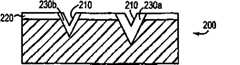
Fig. 2 A shows the vertical view of the part of thesubstrate 200 with the trickle depression figure that constitutes according to the present invention.According to the present invention, characteristic size is typically the hundreds of nanometer to several microns, but greater or lesser feature also is possible.Utilize molding methods, can makesubstrate 200, or itself can be the master that is used for producing mould from master; Selectively, the substrate itself that has been corroded can be used as the basis of microelectronic component.The making of the representative part of microelectronic component has been described in following discussion, and wherein each conductive path or foundation perhaps do not connect via the connection of nonlinear device (for example diode, transistor etc.) to adjacent path.A series ofrow 210 androw 220 are corroded and enter into substrate 200.Usually,row 210 androw 220 are perpendicular each other, and intersects at the matrix place in the hole 230 of change in depth.The degree of depth in hole 230 is decided by to determine at the substrate surface place the foursquare size (that is area) at 230 tops, hole.By means of selecting different square dimensions, can select the equal degree of depth for the conical pit that obtains.For the skilled person in semiconductor and MEMS manufacturing field, the formation of this structure is well-known.
In one embodiment, utilize the silicon corrosion inKOH formation row 210 and row 220.The result of etching process is a plurality ofhollow place 230a and pitting 230b, is referred to as hole 230.In one embodiment, the hole 230 is conical in shape, androw 210 androw 220 are V-shaped grooves, though other shape also is possible.In a specific embodiments, in 100 ml waters under the concentration and 85 ℃ temperature of 44 grams, the corrosion rate of KOH is along<100〉crystal orientation being 1.4 microns of per minutes, and only is 0.0035 micron of per minute along<111〉crystal orientation.As a result, when forming conical pit 230, just form with level and become about 54.74 to spend the sidewall at angles, and will have effective corrosion and fail.Control the desired depth ofrow 210 androw 220 by selecting its width.As shown in the figure, for higher conductivity is provided, can adopt two respectively to be half row side byside 220 ofrow 210 width.This causes having the pairedrow 220 of the gross area that approximately is same as row 210.In this embodiment, the degree of depth ofrow 210 is about two times ofrow 220 degree of depth.Whether form at its infall between hole 230 the degree of depth has been determined row and has been listed as and be connected.
Fig. 2 B and 2C profile illustrate and finish fruit.Becauserow 220 androw 210 are V-shaped grooves, thus among Fig. 2 B amongvisible row 210 parts and Fig. 2 Cvisible row 220 parts dwindle that is angled towards plan.Equally, the rear wall in visible hole 230 also dwindles in Fig. 2 B and 2C, and performance is fallen out and 220 entered the superficial orrow 210 in hole to enter the holedeep.Row 210 is almost same dark withpitting 230b.
In fact, seem may be unlike the final etch pattern shown in Fig. 2 A vertical view for the etching mask of this array.This be because the etch stop layer of KOH do not touched<111〉plane on; If this plane interrupted by another corrosion surface, then corrosion will continue, until reach and do not touched<111〉surface, promptly whole silicon area is eliminated.Circular KOH corrosion is with its mask of undercutting, until forming foursquare conical pit.These etching characteristics are discussed in more detail below.
Can obtain the actual formation of the etch pattern shown in Fig. 2 A with several method.A kind of method is to corroderow 210 androw 220 with a KOH.Masked surface then is so that only expose the square that forms hole 230.Square mask window should be to make hole 230 at the known distance place of lower face and the size in desirable hole 230.The corrosion (for example RIE corrosion) that the surface will be produced vertical sidewall then anisotropically erodes to this degree of depth.Then carry out KOH corrosion regularly, the degree of depth remaining in the hole 230 is corroded.Because these remaining degree of depth are corroded, so each zone, the top of these square conical pits (the bottom upper section of RIE corrosion) will corrode widelyer than the square of its original RIE corrosion owing to seeking<111〉plane.By means ofrow 210 is corroded the square hole that becomes overlapping slightly with each interconnection rectangle ofrow 220, this time corrosion of hole top area will cause that hole 230 corrosion enter each rectangular terminal, thereby form desirable surface topography.The corrosion in back is timed, and causes interconnection to merge with square fully; That is interconnection does not have any shallow seam (as may occurring) with the foursquare tie point place that is connected when corrosion is not enough, and must not be made the effect of depth of interconnection to its middle part by excessive corrosion.In single timing KOH corrosion, form the square hole and the two other mask graph of interconnecting also is possible.Under the situation of KOH corrosion,, can control the degree of depth ofdesirable row 210 androw 220 by selecting the width of row and column.
Under the situation of silicon substrate, as mentioned above, utilize KOH corrosion will form and approximately become 54.74 to spend angles and when forming conical pit, have the sidewall of effective etch stop layer with level.The holder surface characteristics is a rectangle, and then the minor face size will determine the degree of depth in hole. if surface size is 1 micron, then tapered feature about 7072 that will be corroded are dark.If growth thickness is that (this consumes the silicon face of about 450 for the oxide of 1000 , and on original silicon face, produce the oxide surface of about 550 ), the degree of depth in the hole that then obtains will be about 6120 from the original horizontal survey of silicon face, and will be about 6670 from new oxide surface measurement.It is wide that this hole will be about 8652 at the original level of silicon face place, and it is wide to be about 10286 (1.0286 microns) in the surface of new oxide.If wish to have the surface characteristics of different size, then all these sizes can convert in proportion.
This geometric another effect is, if come deposition materials with the linear depositing technics such as electron beam evaporation opposite with the more consistent depositing technics of sputter and so on, be deposited on material layer on the wafer can cause perpendicular to the thickness of the conical pit wall walls of 54.74 degree angles (that is become) measurement with wafer surface only 0.5773 times to the coating of surface deposition.
Though substrate can directly be used, preferably follow the listed formality of Fig. 1, and use the substrate be corroded as master.The technology of molding, impression, mold pressing and spin-on glasses (SOG) and so on can be used to duplicate trickle depression figure, thus produce applied a plurality of material layers duplicate substrate 200 ' so that produce microelectronic component.In order to produce the substrate that duplicates, at first apply the master of electrical forming, then by delamination (, can before SOG, release agent or monolayer material being spun on the master of electrical forming) in order to reduce the adhesiveness of SOG with the SOG technology with the SOG technology.Selectively, polyimide material is deposited on the master of electrical forming, can uses mode delamination then similar in appearance to the SOG method.Be immersed in the deionized water (DI water) by means of the electrical forming master that polyimides is applied, or if the master of electrical forming is applied with thin layer silicon dioxide, then be immersed in the hydrofluoric acid (HF) by means of the electrical forming master that will be applied with polyimides, some polyimides can break away from from the surface.These two kinds of methods all require the master of electrical forming to can't help can make with the material of DI or HF reaction respectively, and for person skilled in the art, these materials are well-known.
In the general introduction of reference Fig. 3, shown series of steps is used to make memory device, wherein is connected binary condition of (utilizing nonlinear device) expression between the row of Jiao Chaing and the raceway groove, does not connect and then represents another state.At first, series of layers is applied to the substrate (step 300) that duplicates.Subsequently, each layer got back to the surface (step 310) that is replicated substrate 200 ' by leveling.Then, carry out corrosion of metals (step 320) regularly, corrode (step 330) with silicon regularly thereupon.Apply insulating barrier (step 340), then leveling (step 350).Will from each layer apply originally and any barrier material that subsequently leveling (step 300-310) stays erodes (step 360).At last, deposited metal (step 370) also flattens metal level (step 380), thereby produces memory device.
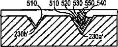
In Fig. 4, Fig. 5 A and Fig. 5 B, illustrated in greater detail deposit (step 300) with the series layer of 500 overall expressions.(should be noted that subsequently paired accompanying drawing presentation graphs 2B and section identical shown in the 2C).With reference to these figure,, then apply insulating barrier (step 400, not shown in Fig. 5 A and 5B) if the substrate 200 ' that duplicates does not insulate.In the illustrated embodiment, deposit the bottom metal layers 510 (step 410) of 1000 , respectively thereupon with the N of 250+Amorphous silicon (N+α Si:H) layer 520 (step 420), α Si:H layer 530 (step 430) of 1000 , metal layer at top 540 (step 440) and the barrier layer 550 (step 450) of 1000 .Bottom metal layers 510 and metal layer attop 540 can be tungsten, chromium or molybdenum, andbarrier layer 550 can be a silicon nitride.The selection of the metal of metal layer attop 510 andbottom metal layers 540 and their thickness, not critical to the present invention, as long as keep the functional requirement of device.
For example,bottom metal layers 510 can be by making with thedirect layer 520 any material that forms ohmic contact thereon.Selectively,bottom metal layers 510 should be thick be enough to carry the electric current that is suitable for any circuit capacitance is provided requiredoperating rate.Layer 520 can be to form any suitable semiconductor that ohmic contact is connected with direct inbottom metal layers 510 between thelayer 530 on the layer 520.Layer 520 should be thick be enough to prevent thatbottom metal layers 510 andlayer 530 are with nonlinear way interact (that is nonrectifying contact).Layer 530 can be to form any material that rectifications contacts (for example the alpha-T6 material of amorphous silicon, Lucent manufacturing or comprise the organic semiconducting materials that is used for making Organic Light Emitting Diode (OLED)) with metal layer at top 540.Layer 530 should be thick be enough to produce the required suitable junction depth of the appropriate work of rectification contact.Metal layer attop 540 can be to form any material that rectifications contact withdirect layer 530 under it.In one embodiment, come applied layer 500, though other conventional deposition process also is possible with chemical vapor deposition (CVD) method.
Be used to replace conical pit if depart from foursquare hole, then when these layers when being corroded, all thickness should approach be enough to not produce regulation design feature size unacceptable shape than (that is for its width and the very high and thin zone between each row or column of Yan Taigao).And, as thin-film transistor (TFT) is made field skilled person understanding, should avoid some material.For example, amorphous silicon is deposited on 200-400 ℃ or above generation.It is stable that deposit metal thereon should keep in deposition process, so that with the silicon of deposit disadvantageous reaction does not take place.Continuous reaction can take place with the grain boundary of amorphous silicon in some metal such as aluminium, even thereby also be inappropriate as top metal, unless add extra barrier metal.
Referring again to Fig. 3, in case apply, layer 500 is just by leveling (step 310).Fig. 6 A and 6B show and flatten all material simultaneously so that the result who highly is consistent with substrate 200.In an optional embodiment, finish this leveling with the combination of CMP and corrosion.With reference to Fig. 6 A and 6B, the CMP polishing step has been scavenged intobarrier layer 550 and metal layer at top 540 peak of amorphous silicon layer 530.Subsequently, carry out regularly corrosion, so that the height that the height ofamorphous silicon layer 530 is reduced to substrate 200 ' meets.At last, repeat the CMP polishing step, so that remove the metal layer attop 550 or thebottom metal layers 510 of substrate 200 ' lip-deep any reservation.Selectively, can adopt other flatening method, for example oxide leveling, wherein, with non-conformal mode deposited oxide material (or material) from the teeth outwards, so that it has an even surface to be corroded with surfacing speed much at one to be flattened.Because this material is corroded, thus the thickness of oxide and surfacing be reduced, until reaching the required smooth degree of depth.This technology and other technology are known person skilled in the art.
Shown in Fig. 7 A and 7B, regularly corrosion of metals (step 320) has been removed not by themetal level barrier layer 550 orsilicon layer depression 560 inhole 230a ' and 230b '.In addition, themetal level row 220 also is eliminated, thereby has isolated eachconductive row 210.
Then, regularly the silicon of any exposure ofsilicon layer hollow place 230a '.As mentioned above,hollow place 230a ' determines thatrow 210 androw 220 intersect wherein to form non-linear element.Eachhollow place 230a ' keeps one deck N+Amorphous silicon 520 and one deckamorphous silicon 530, they form diode (for example Schottky diode) jointly.This N+Lower metal layer 510 in dopedlayer 520 and therow 210 forms ohmic contact, and theamorphous silicon layer 530 that is not doped forms Schottky barriers, therow 220 that are connected to as described below with metal layer attop 540.
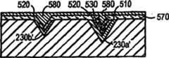
Insulating barrier (for example silica) deposit (step 340) of using the common process such as plasma enhanced CVD (PECVD) or sputter to carry out causes the structure shown in Fig. 9 A and the 9B.Hole 230 ' conical in shape causes the barrier layer 550 (because insulating material is not easy to enter barrier layer 550 belows) that not exclusively is capped.If hole 230 has the sidewall of straight (vertical) sidewall rather than band angle, or if deposit is carried out more more conformally, then the sidewall of barrier material may be applied by extremely thin insulating material.Immerse by means of corrosion regularly fast and to remove that this sidewall applies and the body that reduces illuvium then may correct this not obviously.Extend in the level that the insulating barrier 570 on the substrate 200 ' is got back to substrate 200 ' by leveling.Figure 10 A and Figure 10 B show the not insulated barrier layer 550 that is exposed among the hollow place 230a '.Shown in Figure 11 A and Figure 11 B, the barrier layer 550 that exposes is eroded (step 360), just exposed the metal layer at top 540 among the dell 230a '.Selectively, can omit this polishing step, and as only eroding potential barrier usually doing in the stripping technology, this also will remove insulating material from barrier material.After removing barrier material, the metal among the darker hole 230a ' hole of non-linear element (that is wherein wish to form) on the silicon materials top just is exposed.
The last metal level 580 (step 370) of deposit on the top of insulating barrier 570.Shown in Figure 12 A and 12B, partfinal metal layer 580 extends on thesubstrate 200 '.The level that this part is got back to substrate 200 ' by leveling.Can discern conducting metal that obtains capable 210 androw 220 now, Figure 13 A and 13B show this microelectronic circuit.The material layer that is suitable for forming the conductive path able to programme such as fuse, anti-fuse, variable-resistance material (for example phase change material) by means of adding, according to the present invention with and whole contents be listed in the diode array of the United States Patent (USP) 5673218 of reference herein, can be made into the one or many programmable storage.In this change, can use electric pathway to form all storage locations (that is all forming) with the darkest hole from metal layer at top to the bottom metal level identically.
The feature of substrate is illustrated as forming with above-mentioned KOH herein, but may be timed the RIE corrosion of controlling corrosion depth (feature may have more depart from foursquare shape) in the case, or chemical corrosion (feature wherein may have more reversing mushroom cap shape) forms with a series of.Because the degree of depth in hole and the width of surface (not being the width of its bottom) are constructed the key factor according to device of the present invention just, so formal the use thus departed from feature foursquare or the mushroom hat.Should be noted that, produced the track continuity of vertical sidewall place for corrosion from a kind of feature of the degree of depth to the feature of adjacent different depth, should adopt conformal deposition, so that guarantee that rising to sidewall in a kind of bottom of feature connects to forming between the bottom of adjacent feature.
Figure 14 shows the another kind of technology that is used for forming substrate feature.Utilize this method, produced etching mask 600, it comprises the feature 610a or the 610b (being generically and collectively referred to as 610) in each hole 230, but does not comprise the raceway groove that connects each hole 230.These mask features 610 can be formed a kind of corresponding in two kinds of sizes of two kinds of different holes degree of depth.Figure 14 shows has circular feature 610; But also can producing wherein, feature 610 has the mask (that is the orientation of the square in the hole of diamond orientations mask window) that becomes the square shape of miter angle orientation with the etch pit that obtains.The orientation of the row and column of mask and<111〉silicon crystal orientation departs from 45 degree.As shown in figure 14, KOH corrodes this mask shape of undercutting, to reach the taper etch stop layer, unless this undercutting is formed the raceway groove between each hole by the merging of the corner of adjacent feature.Bigger feature 610b will cause darker hole, and less feature 610a will cause more shallow hole.More close feature 610 (that is forming the circle of going) will have darker raceway groove, and wideer at interval feature (that is forming the circle that is listed as) will have more shallow raceway groove.The size of circle and being selected at interval makes any two its sizes of adjacent circle all cause making only suitable surplus material layer to be retained in channel depth in therebetween the raceway groove.Utilize this method, the degree of depth in hole is by the etch stop layer control of nature, and channel depth is regularly controlled by corrosion.For the degree of depth that helps to guarantee to cheat since time that raceway groove has formed and reaching fully can carry out initial RIE corrosion as mentioned above.If produce substrate, then, can select two kinds of mask feature size, thereby can draw the great circle feature with the beam power higher than roundlet feature by means of the power that changes electron beam with electron beam lithography.The characteristic that focuses on the exposure test will be determined the suitable power level of two kinds of characteristic sizes.
The present invention is based on each layer of being deposited on the section substrate and can is processed to make the material that stays to form wherein feature by the method for self aligned circuit by leveling and corrosion.The differing heights of surface before deposition of materials determined along with surperficial any one which material of set point place of going up of the carrying out of leveling is exposed.Can also optionally process the surface of exposure by corrosion.Can predict hole with several different in width and degree of depth, thus can iterative process so that produce comprise a plurality of material layers can make the more hole of complex devices.For example, utilize to add thin dielectric layer, can make up the transistor of TFT class.
The present invention can comprise other processing step.For example, the occasion of metal area for the treatment of to become solder joint of the feature bottom of being formed at is being arranged, deposit top metal on the surface that does not have insulatingmaterial 570 andsemi-conducting material
Illustrated after each preferred embodiment that person skilled in the art are appreciated that various changes are possible in the present invention's scope required for protection and design.Therefore think that the present invention is only limited by the scope of claim.
Claims (28)
Translated fromChineseApplications Claiming Priority (2)
| Application Number | Priority Date | Filing Date | Title |
|---|---|---|---|
| US23585300P | 2000-09-27 | 2000-09-27 | |
| US60/235,853 | 2000-09-27 |
Publications (2)
| Publication Number | Publication Date |
|---|---|
| CN1476637Atrue CN1476637A (en) | 2004-02-18 |
| CN100435347C CN100435347C (en) | 2008-11-19 |
Family
ID=22887168
Family Applications (1)
| Application Number | Title | Priority Date | Filing Date |
|---|---|---|---|
| CNB01819463XAExpired - Fee RelatedCN100435347C (en) | 2000-09-27 | 2001-09-27 | Manufacturing of Semiconductor Devices |
Country Status (6)
| Country | Link |
|---|---|
| US (3) | US6586327B2 (en) |
| EP (1) | EP1320872A2 (en) |
| JP (1) | JP2004523881A (en) |
| CN (1) | CN100435347C (en) |
| AU (1) | AU2001294817A1 (en) |
| WO (1) | WO2002027768A2 (en) |
Families Citing this family (45)
| Publication number | Priority date | Publication date | Assignee | Title |
|---|---|---|---|---|
| US5673218A (en) | 1996-03-05 | 1997-09-30 | Shepard; Daniel R. | Dual-addressed rectifier storage device |
| US6956757B2 (en)* | 2000-06-22 | 2005-10-18 | Contour Semiconductor, Inc. | Low cost high density rectifier matrix memory |
| WO2002027768A2 (en) | 2000-09-27 | 2002-04-04 | Nüp2 Incorporated | Fabrication of semiconductor devices |
| US6713408B1 (en)* | 2000-12-14 | 2004-03-30 | Louisiana Tech University Foundation, Inc. | Method of producing silica micro-structures from x-ray lithography of SOG materials |
| US20030006527A1 (en)* | 2001-06-22 | 2003-01-09 | Rabolt John F. | Method of fabricating micron-and submicron-scale elastomeric templates for surface patterning |
| US6875695B2 (en)* | 2002-04-05 | 2005-04-05 | Mems Optical Inc. | System and method for analog replication of microdevices having a desired surface contour |
| US7376008B2 (en)* | 2003-08-07 | 2008-05-20 | Contour Seminconductor, Inc. | SCR matrix storage device |
| US20050067675A1 (en)* | 2003-08-19 | 2005-03-31 | Shepard Daniel Robert | Molded substrate for topograpy based lithography |
| PL1663349T3 (en)* | 2003-09-22 | 2008-10-31 | Innovation Tech Inc Gainesville | Wound irrigation device and method |
| US20050129843A1 (en)* | 2003-12-11 | 2005-06-16 | Xerox Corporation | Nanoparticle deposition process |
| US8148251B2 (en) | 2004-01-30 | 2012-04-03 | Hewlett-Packard Development Company, L.P. | Forming a semiconductor device |
| US7195950B2 (en)* | 2004-07-21 | 2007-03-27 | Hewlett-Packard Development Company, L.P. | Forming a plurality of thin-film devices |
| KR100661347B1 (en)* | 2004-10-27 | 2006-12-27 | 삼성전자주식회사 | Micro thin film structure and MEMS switch using the same and method for manufacturing them |
| FR2880191B1 (en)* | 2004-12-23 | 2007-03-16 | St Microelectronics Sa | ACHIEVING TRENCHES OR WELLS HAVING DIFFERENT DESTINATIONS IN A SEMICONDUCTOR SUBSTRATE |
| KR100670538B1 (en)* | 2004-12-30 | 2007-01-16 | 매그나칩 반도체 유한회사 | Image sensor and its manufacturing method that can improve optical characteristics |
| US8048789B2 (en)* | 2005-04-26 | 2011-11-01 | Northwestern University | Mesoscale pyramids, arrays and methods of preparation |
| US7446345B2 (en)* | 2005-04-29 | 2008-11-04 | Cree, Inc. | Light emitting devices with active layers that extend into opened pits |
| CN101287857B (en)* | 2005-05-05 | 2011-07-13 | H.C.施塔克有限公司 | Coating method for manufacturing or reprocessing sputtering targets and X-ray anodes |
| US8802191B2 (en)* | 2005-05-05 | 2014-08-12 | H. C. Starck Gmbh | Method for coating a substrate surface and coated product |
| US7667996B2 (en)* | 2006-02-15 | 2010-02-23 | Contour Semiconductor, Inc. | Nano-vacuum-tubes and their application in storage devices |
| US7593256B2 (en)* | 2006-03-28 | 2009-09-22 | Contour Semiconductor, Inc. | Memory array with readout isolation |
| US20080023694A1 (en)* | 2006-07-25 | 2008-01-31 | Chi Mei El Corp. | Display device and method of manufacturing the same |
| US7479671B2 (en)* | 2006-08-29 | 2009-01-20 | International Business Machines Corporation | Thin film phase change memory cell formed on silicon-on-insulator substrate |
| US20080078268A1 (en)* | 2006-10-03 | 2008-04-03 | H.C. Starck Inc. | Process for preparing metal powders having low oxygen content, powders so-produced and uses thereof |
| JP5377319B2 (en)* | 2006-11-07 | 2013-12-25 | ハー.ツェー.スタルク ゲゼルシャフト ミット ベシュレンクテル ハフツング | Substrate coating method and coated product |
| US20080145688A1 (en) | 2006-12-13 | 2008-06-19 | H.C. Starck Inc. | Method of joining tantalum clade steel structures |
| US8157914B1 (en) | 2007-02-07 | 2012-04-17 | Chien-Min Sung | Substrate surface modifications for compositional gradation of crystalline materials and associated products |
| US7576364B2 (en)* | 2007-02-15 | 2009-08-18 | Chi Mei Optoelectronics Corp. | Display device and method of manufacturing the same |
| US8197894B2 (en) | 2007-05-04 | 2012-06-12 | H.C. Starck Gmbh | Methods of forming sputtering targets |
| US7799600B2 (en)* | 2007-05-31 | 2010-09-21 | Chien-Min Sung | Doped diamond LED devices and associated methods |
| US7813157B2 (en)* | 2007-10-29 | 2010-10-12 | Contour Semiconductor, Inc. | Non-linear conductor memory |
| WO2009086084A1 (en)* | 2007-12-19 | 2009-07-09 | Contour Semiconductor, Inc. | Field-emitter-based memory array with phase-change storage devices |
| US20090225621A1 (en)* | 2008-03-05 | 2009-09-10 | Shepard Daniel R | Split decoder storage array and methods of forming the same |
| US20090296445A1 (en)* | 2008-06-02 | 2009-12-03 | Shepard Daniel R | Diode decoder array with non-sequential layout and methods of forming the same |
| WO2010022036A2 (en)* | 2008-08-18 | 2010-02-25 | Contour Semiconductor, Inc. | Method for forming self-aligned phase-change semiconductor diode memory |
| US8246903B2 (en) | 2008-09-09 | 2012-08-21 | H.C. Starck Inc. | Dynamic dehydriding of refractory metal powders |
| US8043655B2 (en)* | 2008-10-06 | 2011-10-25 | H.C. Starck, Inc. | Low-energy method of manufacturing bulk metallic structures with submicron grain sizes |
| US8325556B2 (en)* | 2008-10-07 | 2012-12-04 | Contour Semiconductor, Inc. | Sequencing decoder circuit |
| US20100096610A1 (en)* | 2008-10-17 | 2010-04-22 | Wang Hsingya A | Phase-change material memory cell |
| US20100165727A1 (en)* | 2008-12-31 | 2010-07-01 | Shepard Daniel R | Phase change material memory having no erase cycle |
| US8773881B2 (en) | 2009-03-10 | 2014-07-08 | Contour Semiconductor, Inc. | Vertical switch three-dimensional memory array |
| US9412568B2 (en) | 2011-09-29 | 2016-08-09 | H.C. Starck, Inc. | Large-area sputtering targets |
| WO2014089214A2 (en) | 2012-12-04 | 2014-06-12 | William Marsh Rice University | Carbonaceous nanoparticles as conductivity enhancement additives to water-in-oil emulsions, oil-in-water emulsions and oil-based wellbore fluids |
| US20160315256A1 (en)* | 2013-12-13 | 2016-10-27 | Hewlett Packard Enterprise Development Lp | V-shape resistive memory element |
| US10818778B2 (en) | 2017-11-27 | 2020-10-27 | Taiwan Semiconductor Manufacturing Co., Ltd. | Heterogeneous semiconductor device substrates with high quality epitaxy |
Family Cites Families (34)
| Publication number | Priority date | Publication date | Assignee | Title |
|---|---|---|---|---|
| US324051A (en)* | 1885-08-11 | Wilhblm umland | ||
| US3245051A (en) | 1960-11-16 | 1966-04-05 | John H Robb | Information storage matrices |
| BE757340A (en)* | 1969-10-09 | 1971-03-16 | Mercury Outboard Motors South | IMPROVEMENTS TO PRESS PUNCHES AND DIES |
| US4369564A (en)* | 1979-10-29 | 1983-01-25 | American Microsystems, Inc. | VMOS Memory cell and method for making same |
| US5173442A (en)* | 1990-07-23 | 1992-12-22 | Microelectronics And Computer Technology Corporation | Methods of forming channels and vias in insulating layers |
| JPH06215423A (en)* | 1992-11-26 | 1994-08-05 | Canon Inc | Optical recording medium substrate sheet manufacturing method and manufacturing apparatus, stamper manufacturing method, and photomask manufacturing method |
| US5244837A (en) | 1993-03-19 | 1993-09-14 | Micron Semiconductor, Inc. | Semiconductor electrical interconnection methods |
| JPH0766438A (en) | 1993-08-30 | 1995-03-10 | Tonen Corp | Method for manufacturing substrate for photoelectric conversion device |
| JPH07334866A (en)* | 1994-04-14 | 1995-12-22 | Pioneer Electron Corp | Optical disk and its production |
| US5831276A (en) | 1995-06-07 | 1998-11-03 | Micron Technology, Inc. | Three-dimensional container diode for use with multi-state material in a non-volatile memory cell |
| US6420725B1 (en)* | 1995-06-07 | 2002-07-16 | Micron Technology, Inc. | Method and apparatus for forming an integrated circuit electrode having a reduced contact area |
| US6309580B1 (en)* | 1995-11-15 | 2001-10-30 | Regents Of The University Of Minnesota | Release surfaces, particularly for use in nanoimprint lithography |
| US5673218A (en) | 1996-03-05 | 1997-09-30 | Shepard; Daniel R. | Dual-addressed rectifier storage device |
| JP3607424B2 (en) | 1996-07-12 | 2005-01-05 | 株式会社東芝 | Semiconductor device and manufacturing method thereof |
| JP3441312B2 (en) | 1996-09-18 | 2003-09-02 | 株式会社東芝 | Field emission cold cathode device and method of manufacturing the same |
| US5859964A (en) | 1996-10-25 | 1999-01-12 | Advanced Micro Devices, Inc. | System and method for performing real time data acquisition, process modeling and fault detection of wafer fabrication processes |
| WO1999039394A1 (en) | 1998-02-02 | 1999-08-05 | Uniax Corporation | X-y addressable electric microswitch arrays and sensor matrices employing them |
| JPH11305055A (en)* | 1998-04-22 | 1999-11-05 | Sharp Corp | Method of manufacturing optical waveguide and method of manufacturing master master plate for manufacturing optical waveguide |
| US6713238B1 (en)* | 1998-10-09 | 2004-03-30 | Stephen Y. Chou | Microscale patterning and articles formed thereby |
| US6815774B1 (en)* | 1998-10-29 | 2004-11-09 | Mitsubishi Materials Silicon Corporation | Dielectrically separated wafer and method of the same |
| JP2000133704A (en)* | 1998-10-29 | 2000-05-12 | Mitsubishi Materials Silicon Corp | Dielectric isolation wafer and its manufacture |
| US6256767B1 (en) | 1999-03-29 | 2001-07-03 | Hewlett-Packard Company | Demultiplexer for a molecular wire crossbar network (MWCN DEMUX) |
| US6190929B1 (en)* | 1999-07-23 | 2001-02-20 | Micron Technology, Inc. | Methods of forming semiconductor devices and methods of forming field emission displays |
| TW432546B (en)* | 1999-11-25 | 2001-05-01 | Taiwan Semiconductor Mfg | Manufacturing method of copper damascene |
| JP2001217245A (en)* | 2000-02-04 | 2001-08-10 | Sharp Corp | Electronic component and manufacturing method thereof |
| WO2002027768A2 (en) | 2000-09-27 | 2002-04-04 | Nüp2 Incorporated | Fabrication of semiconductor devices |
| US6817531B2 (en) | 2001-03-07 | 2004-11-16 | Hewlett-Packard Development Company, L.P. | Apparatus and methods for marking content of memory storage devices |
| US7039780B2 (en) | 2001-06-05 | 2006-05-02 | Hewlett-Packard Development Company, L.P. | Digital camera memory system |
| US6567295B2 (en) | 2001-06-05 | 2003-05-20 | Hewlett-Packard Development Company, L.P. | Addressing and sensing a cross-point diode memory array |
| US6385075B1 (en) | 2001-06-05 | 2002-05-07 | Hewlett-Packard Company | Parallel access of cross-point diode memory arrays |
| US6552409B2 (en) | 2001-06-05 | 2003-04-22 | Hewlett-Packard Development Company, Lp | Techniques for addressing cross-point diode memory arrays |
| US6646912B2 (en) | 2001-06-05 | 2003-11-11 | Hewlett-Packard Development Company, Lp. | Non-volatile memory |
| US6478231B1 (en) | 2001-06-29 | 2002-11-12 | Hewlett Packard Company | Methods for reducing the number of interconnects to the PIRM memory module |
| US6599796B2 (en) | 2001-06-29 | 2003-07-29 | Hewlett-Packard Development Company, L.P. | Apparatus and fabrication process to reduce crosstalk in pirm memory array |
- 2001
- 2001-09-27WOPCT/US2001/030296patent/WO2002027768A2/enactiveApplication Filing
- 2001-09-27JPJP2002531468Apatent/JP2004523881A/enactivePending
- 2001-09-27AUAU2001294817Apatent/AU2001294817A1/ennot_activeAbandoned
- 2001-09-27EPEP01975498Apatent/EP1320872A2/ennot_activeWithdrawn
- 2001-09-27USUS09/965,622patent/US6586327B2/ennot_activeExpired - Lifetime
- 2001-09-27CNCNB01819463XApatent/CN100435347C/ennot_activeExpired - Fee Related
- 2003
- 2003-06-11USUS10/459,699patent/US7183206B2/ennot_activeExpired - Lifetime
- 2007
- 2007-01-19USUS11/655,470patent/US7507663B2/ennot_activeExpired - Fee Related
Also Published As
| Publication number | Publication date |
|---|---|
| US7507663B2 (en) | 2009-03-24 |
| JP2004523881A (en) | 2004-08-05 |
| US20070117388A1 (en) | 2007-05-24 |
| US20040132288A1 (en) | 2004-07-08 |
| US7183206B2 (en) | 2007-02-27 |
| WO2002027768A3 (en) | 2002-08-22 |
| EP1320872A2 (en) | 2003-06-25 |
| WO2002027768A2 (en) | 2002-04-04 |
| AU2001294817A1 (en) | 2002-04-08 |
| US20020086542A1 (en) | 2002-07-04 |
| US6586327B2 (en) | 2003-07-01 |
| CN100435347C (en) | 2008-11-19 |
Similar Documents
| Publication | Publication Date | Title |
|---|---|---|
| CN1476637A (en) | Manufacturing of Semiconductor Devices | |
| CN1292628C (en) | Methods of Forming Inductors and Channels in Monolithic Circuits | |
| US8937011B2 (en) | Method of forming crack free gap fill | |
| KR20030003106A (en) | Apparatus and fabrication process to reduce crosstalk in pirm memory array | |
| US20050142863A1 (en) | Process for forming tapered trenches in a dielectric material | |
| US9633986B2 (en) | Technique for fabrication of microelectronic capacitors and resistors | |
| CN112117298B (en) | Three-dimensional phase change memory and preparation method thereof | |
| CN109494192A (en) | Semiconductor element and manufacturing method thereof | |
| CN114823677A (en) | semiconductor device | |
| US20070254428A1 (en) | Integrated circuit including resistivity changing memory cells | |
| WO2003036711A3 (en) | Fill pattern generation for spin-on glass and related self-planarization deposition | |
| US7682942B2 (en) | Method for reducing pillar structure dimensions of a semiconductor device | |
| US5045917A (en) | Multi-level semiconductor structure and process of fabricating thereof | |
| US7677701B2 (en) | Micro-fluid ejection head with embedded chip on non-conventional substrate | |
| US11355348B2 (en) | Integrated circuit, construction of integrated circuitry, and method of forming an array | |
| CN1236974A (en) | Method for manufacturing semiconductor memory device using two etching patterns | |
| CN1243379C (en) | Method for fabricating MIM capacitors in copper damascene process | |
| KR100258366B1 (en) | Planarization method of semiconductor device | |
| KR100190079B1 (en) | Metal wiring of semiconductor device and forming method thereof | |
| CN1841698A (en) | Method for fabricating semiconductor device | |
| CN1399330A (en) | Method for manufacturing electrical insulating layer on bit line of flash memory | |
| KR20040038139A (en) | Method of forming tungsten contact plug of semiconductor device | |
| CN1520236A (en) | Active organic light emitting display device and method of manufacturing the same | |
| KR980005483A (en) | Method for manufacturing charge storage electrode of semiconductor device | |
| KR20030050655A (en) | Method for forming contact in semiconductor device |
Legal Events
| Date | Code | Title | Description |
|---|---|---|---|
| C06 | Publication | ||
| PB01 | Publication | ||
| C10 | Entry into substantive examination | ||
| SE01 | Entry into force of request for substantive examination | ||
| C14 | Grant of patent or utility model | ||
| GR01 | Patent grant | ||
| C56 | Change in the name or address of the patentee | ||
| CP03 | Change of name, title or address | Address after:California, USA Patentee after:HGST Co. Address before:New Hampshire Patentee before:NuP2 Inc. | |
| C41 | Transfer of patent application or patent right or utility model | ||
| C56 | Change in the name or address of the patentee | ||
| CP01 | Change in the name or title of a patent holder | Address after:New Hampshire Patentee after:CONTOUR SEMICONDUCTOR, Inc. Address before:New Hampshire Patentee before:NuP2 Inc. | |
| TR01 | Transfer of patent right | Effective date of registration:20160819 Address after:California, USA Patentee after:HGST Co. Address before:New Hampshire Patentee before:CONTOUR SEMICONDUCTOR, Inc. | |
| TR01 | Transfer of patent right | ||
| TR01 | Transfer of patent right | Effective date of registration:20180907 Address after:California, USA Patentee after:Western Digital Technologies, Inc. Address before:California, USA Patentee before:HGST Co. | |
| CF01 | Termination of patent right due to non-payment of annual fee | ||
| CF01 | Termination of patent right due to non-payment of annual fee | Granted publication date:20081119 Termination date:20200927 |