CN1467746A - Semiconductor memory with improved recovery rate of defective chips - Google Patents
Semiconductor memory with improved recovery rate of defective chipsDownload PDFInfo
- Publication number
- CN1467746A CN1467746ACNA031205143ACN03120514ACN1467746ACN 1467746 ACN1467746 ACN 1467746ACN A031205143 ACNA031205143 ACN A031205143ACN 03120514 ACN03120514 ACN 03120514ACN 1467746 ACN1467746 ACN 1467746A
- Authority
- CN
- China
- Prior art keywords
- mentioned
- address
- circuit
- line
- regular
- Prior art date
- Legal status (The legal status is an assumption and is not a legal conclusion. Google has not performed a legal analysis and makes no representation as to the accuracy of the status listed.)
- Granted
Links
Images


Classifications
- G—PHYSICS
- G11—INFORMATION STORAGE
- G11C—STATIC STORES
- G11C29/00—Checking stores for correct operation ; Subsequent repair; Testing stores during standby or offline operation
- G11C29/70—Masking faults in memories by using spares or by reconfiguring
- G11C29/78—Masking faults in memories by using spares or by reconfiguring using programmable devices
- G11C29/80—Masking faults in memories by using spares or by reconfiguring using programmable devices with improved layout
- G11C29/808—Masking faults in memories by using spares or by reconfiguring using programmable devices with improved layout using a flexible replacement scheme
- G—PHYSICS
- G11—INFORMATION STORAGE
- G11C—STATIC STORES
- G11C29/00—Checking stores for correct operation ; Subsequent repair; Testing stores during standby or offline operation
- G11C29/70—Masking faults in memories by using spares or by reconfiguring
- G11C29/78—Masking faults in memories by using spares or by reconfiguring using programmable devices
- G11C29/84—Masking faults in memories by using spares or by reconfiguring using programmable devices with improved access time or stability
- G11C29/846—Masking faults in memories by using spares or by reconfiguring using programmable devices with improved access time or stability by choosing redundant lines at an output stage
- G—PHYSICS
- G11—INFORMATION STORAGE
- G11C—STATIC STORES
- G11C29/00—Checking stores for correct operation ; Subsequent repair; Testing stores during standby or offline operation
- G11C29/70—Masking faults in memories by using spares or by reconfiguring
- G11C29/78—Masking faults in memories by using spares or by reconfiguring using programmable devices
- G11C29/84—Masking faults in memories by using spares or by reconfiguring using programmable devices with improved access time or stability
- G11C29/848—Masking faults in memories by using spares or by reconfiguring using programmable devices with improved access time or stability by adjacent switching
Landscapes
- For Increasing The Reliability Of Semiconductor Memories (AREA)
- Dram (AREA)
- Tests Of Electronic Circuits (AREA)
Abstract
Translated fromChinese
Description
Translated fromChinese技术领域technical field
本发明涉及半导体存储器,更特定地说,涉及包含能进行由备用存储单元导致的置换的存储单元阵列的的半导体存储器。The present invention relates to semiconductor memories, and more particularly, to semiconductor memories including memory cell arrays capable of replacement by spare memory cells.
背景技术Background technique
近年来,半导体存储器在高集成化方面正日益取得进展。集成度高的半导体存储器具备备用存储单元,一般来说,即使在制造阶段中在一部分的存储单元中产生了缺陷的情况下,也可将该缺陷产生的不良存储单元置换为备用存储单元进行补救。一般使用通过进行这样的冗余置换来提高成品率的方法。In recent years, semiconductor memories are increasingly progressing in high integration. Highly integrated semiconductor memories have spare memory cells. In general, even if a defect occurs in some of the memory cells during the manufacturing process, the defective memory cells caused by the defect can be replaced with spare memory cells for remediation. . A method of improving yield by performing such redundant replacement is generally used.
但是,由于半导体存储器的大规模化的缘故,第1,为了提高成品率,包含成为必要的备用存储单元的元素的数目增大,随之,用来存储应置换备用存储单元的不良存储单元的地址的编程元件的数目也增加了。由于这些要素增加的缘故,发生芯片面积增大的问题。However, due to the increase in the size of semiconductor memories, firstly, in order to improve the yield, the number of elements including the necessary spare memory cells increases, and accordingly, the number of elements used to store the defective memory cells that should be replaced by the spare memory cells The number of address programming elements is also increased. Due to the increase of these factors, there occurs a problem of an increase in the chip area.
为了进行置换,必须以非易失性的方式存储不良存储单元的地址。作为其方法,大多使用熔断元件等的编程元件。使用激光束等来切断该熔断元件。为了可靠地进行切断且不损伤周围的元件,对于熔断元件来说必须有某种程度的大小,此外在其周边不存在其它的元件。因而,具备越多的编程元件,芯片面积就越大。For replacement, the address of the bad memory cell must be stored in a non-volatile manner. As its method, programming elements such as fuse elements are often used. The fuse element is cut using a laser beam or the like. In order to cut off reliably without damaging surrounding elements, it is necessary for the fuse element to be of a certain size, and in addition there are no other elements around it. Therefore, the more programming elements there are, the larger the chip area will be.
此外,第2,随着编程元件数目的增加,用来补救不良芯片的编程时间也不能忽略,发生了制造成本增大的问题。In addition, secondly, as the number of programming elements increases, the programming time for repairing defective chips cannot be ignored, and the problem of increased manufacturing costs arises.
发明内容Contents of the invention
本发明的目的在于提供提高了起因于不良存储单元的不良芯片的补救率的半导体存储器。An object of the present invention is to provide a semiconductor memory in which the recovery rate of defective chips caused by defective memory cells is improved.
如果归纳本发明,则本发明是一种半导体存储器,具备:第1~第4正规存储单元组、第1、第2预备存储单元、第1选择电路和第2选择电路。Summarizing the present invention, the present invention is a semiconductor memory including first to fourth regular memory cell groups, first and second spare memory cells, a first selection circuit, and a second selection circuit.
第1~第4正规存储单元组分别包含多个正规存储单元。Each of the first to fourth regular memory cell groups includes a plurality of regular memory cells.
第1、第2预备存储单元用来对上述多个正规存储单元中的缺陷存储单元进行置换。The first and second spare memory cells are used to replace defective memory cells among the plurality of regular memory cells.
第1选择电路以非易失性的方式保持地址分配信息。第1选择电路响应于作为输入地址所供给的第1地址值,与第1预备存储单元一起选择根据该地址分配信息所决定的第1~第4正规存储单元组中的某2个正规存储单元组。第1选择电路响应于作为输入地址所供给的第2地址值,与第2预备存储单元一起选择根据地址分配信息所决定的第1~第4正规存储单元组中的另外2个正规存储单元组。The first selection circuit holds address assignment information in a non-volatile manner. In response to the first address value supplied as the input address, the first selection circuit selects, together with the first spare memory cell, any two regular memory cells in the first to fourth regular memory cell groups determined based on the address allocation information. Group. In response to the second address value supplied as the input address, the first selection circuit, together with the second spare memory cell, selects the other two regular memory cell groups among the first to fourth regular memory cell groups determined based on the address allocation information. .
第2选择电路以非易失性的方式保持置换信息。第2选择电路根据该置换信息选择第1预备存储单元来代替根据第1地址值所选择的正规存储单元中的第1缺陷存储单元。第2选择电路根据置换信息选择第2预备存储单元来代替根据第2地址值所选择的正规存储单元中的第2缺陷存储单元。The second selection circuit holds replacement information in a nonvolatile manner. The second selection circuit selects the first spare memory cell to replace the first defective memory cell among the regular memory cells selected by the first address value based on the replacement information. The second selection circuit selects the second spare memory cell to replace the second defective memory cell among the regular memory cells selected by the second address value based on the replacement information.
因而,本发明的主要的优点是既可抑制预备存储单元数目的增加,又可提高由预备存储单元得到的不良芯片的补救率。Therefore, the main advantage of the present invention is that it can suppress the increase of the number of spare storage units and improve the recovery rate of defective chips obtained from the spare storage units.
通过参照附图的后述的本发明的详细的说明,本发明的上述和其它的目的、特征、方面和优点会变得更加明白。The above and other objects, features, aspects, and advantages of the present invention will become more apparent from the detailed description of the present invention to be described later with reference to the accompanying drawings.
附图说明Description of drawings
图1是示出本发明的实施例1的半导体存储器1的结构的概略框图。FIG. 1 is a schematic block diagram showing the structure of a
图2是概略地示出存储单元阵列14的结构的电路图。FIG. 2 is a circuit diagram schematically showing the structure of the
图3是示出了图1中的SD发生电路4的结构的电路图。FIG. 3 is a circuit diagram showing the structure of the SD generating circuit 4 in FIG. 1 .
图4是示出了图3中的开关电路92的结构的电路图。FIG. 4 is a circuit diagram showing the structure of the
图5是说明虽然以往不能置换但利用本发明成为可置换的不良存储单元的配置用的图。Fig. 5 is a diagram for explaining the disposition of defective memory cells which cannot be replaced conventionally but which can be replaced by the present invention.
图6是说明在本发明的实施例1中进行的存储单元的置换用的图。Fig. 6 is a diagram for explaining memory cell replacement performed in
图7是说明实施例1的变例用的电路图。Fig. 7 is a circuit diagram for explaining a modification of the first embodiment.
图8是示出实施例2的半导体存储器201的结构的框图。FIG. 8 is a block diagram showing the structure of the semiconductor memory 201 of the second embodiment.
图9是说明图8中的行译码器+列译码器202的结构和存储单元阵列214的结构用的图。FIG. 9 is a diagram for explaining the configuration of row decoder+column decoder 202 and the configuration of memory cell array 214 in FIG. 8 .
图10是说明不良部位用的逻辑地址图。Fig. 10 is a logical address diagram for explaining defective parts.
图11是说明实施例2中的存储单元的置换用的图。FIG. 11 is a diagram for explaining replacement of memory cells in the second embodiment.
图12是示出实施例3的半导体存储器301的结构的框图。FIG. 12 is a block diagram showing the structure of a semiconductor memory 301 of the third embodiment.
图13是示出图12中的2对1译码器309的结构的电路图。FIG. 13 is a circuit diagram showing the structure of the 2-to-1
图14是示出图12中的IOS发生电路304的结构的电路图。FIG. 14 is a circuit diagram showing the configuration of the IOS generation circuit 304 in FIG. 12 .
图15是说明在存储单元阵列的1个存储单元行中存在多个不良存储单元的情况用的图。FIG. 15 is a diagram for explaining a case where a plurality of defective memory cells exist in one memory cell row of the memory cell array.
图16是说明行地址的信号位RAx为0时的不良存储单元的置换用的图。FIG. 16 is a diagram for explaining replacement of defective memory cells when the row address signal bit RAx is 0. FIG.
图17是说明行地址的信号位RAx为1时的不良存储单元的置换用的图。FIG. 17 is a diagram for explaining replacement of defective memory cells when the row address signal bit RAx is 1. FIG.
图18是示出实施例4的半导体存储器401的结构的概略框图。FIG. 18 is a schematic block diagram showing the structure of a
图19是示出图18中的IO选择器410的结构的电路图。FIG. 19 is a circuit diagram showing the structure of the
图20是示出实施例5的半导体存储器501的结构的框图。FIG. 20 is a block diagram showing the structure of a semiconductor memory 501 of the fifth embodiment.
图21是示出图20中的IO移动电路510的结构的电路图。FIG. 21 is a circuit diagram showing the structure of the
图22是说明在实施例5中能进行补救的不良存储单元的发生位置用的图。Fig. 22 is a diagram for explaining occurrence locations of defective memory cells that can be remedied in the fifth embodiment.
图23是示出实施例6的半导体存储器601的结构的框图。FIG. 23 is a block diagram showing the structure of the semiconductor memory 601 of the sixth embodiment.
图24是说明地址置换前的不良的位置用的图。Fig. 24 is a diagram for explaining defective positions before address replacement.
图25是示出了能进行地址分配变更后的错误校正的不良的存在部位用的图。FIG. 25 is a diagram showing defective locations where error correction after address allocation change can be performed.
图26是示出实施例7的半导体存储器701的结构的电路图。FIG. 26 is a circuit diagram showing the structure of the
图27是示出了在实施例8的半导体存储器中代替图4中示出的开关电路92而使用的开关电路802的结构的电路图。FIG. 27 is a circuit diagram showing a configuration of a
图28是说明第2测试模式用的图。Fig. 28 is a diagram for explaining the second test mode.
图29是说明组合了图27、图28的变例用的图。Fig. 29 is a diagram for explaining a modification in which Figs. 27 and 28 are combined.
具体实施方式Detailed ways
以下,参照附图详细地说明本发明的实施例。再有,图中同一符号表示同一或相当的部分。Hereinafter, embodiments of the present invention will be described in detail with reference to the drawings. In addition, the same symbol in a drawing represents the same or corresponding part.
〔实施例1〕[Example 1]
图1是示出本发明的实施例1的半导体存储器1的结构的概略框图。FIG. 1 is a schematic block diagram showing the structure of a
参照图1,半导体存储器1包含:行译码器2,用来接受行地址信号RA0~RAk以进行存储单元的行的选择;主字驱动器MWD,根据行译码器2的输出来驱动主字线;以及SD发生电路4,接受行地址信号RA0~RAk,输出信号SD10~SD21。Referring to Fig. 1,
半导体存储器1还包含:地址编程电路6,以非易失性的方式存储与不良存储单元对应的应置换的地址;地址比较器8,比较地址编程电路6的输出与列地址信号CA0~CAn;列译码器10,用来根据地址比较器8的输出决定激活状态,根据列地址信号CA0~CAn进行存储单元的列选择;备用列译码器12,用来根据地址比较器8的输出选择备用存储单元的列;以及存储单元阵列14。The
存储单元阵列14根据行译码器2、列译码器10以及备用列译码器12的输出选择行和列,进行与外部的数据的授受。存储单元阵列14包含子字驱动器SWD和读出放大器带SAB,被子字驱动器SWD和读出放大器带SAB分割为被区分为栅格状的多个存储器块。The
半导体存储器1利用行译码器2、子字驱动器SWD和SD发生电路4进行存储单元的行的选择作为第1阶段,利用地址编程电路6、地址比较器8、列译码器10和备用列译码器12进行存储单元的列的选择作为第2阶段。在该第2阶段的列选择时,进行备用存储单元对于正规存储单元的置换。
图2是概略地示出存储单元阵列14的结构的电路图。再有,为了说明起见,在图中也示出了行译码器2和主字驱动器MWD。FIG. 2 is a circuit diagram schematically showing the structure of the
参照图2,存储单元阵列14包含:子字驱动器带SWD;读出放大器带SAB;以及存储器块BLK11、BLK12、BLK21、BLK22。Referring to FIG. 2, the
子字驱动器带SWD包含:子字驱动器SWD10,根据主字驱动器MWD的输出驱动子字线SWL10;以及子字驱动器SWD11,根据主字驱动器MWD的输出驱动子字线SWL11。子字驱动器SWD10、SWD11是与存储器块BLK11对应地设置的。子字驱动器SWD10、SWD11分别根据信号SD10、信号SD11而被激活。The sub-word driver zone SWD includes: a sub-word driver SWD10 for driving the sub-word line SWL10 according to the output of the main word driver MWD; and a sub-word driver SWD11 for driving the sub-word line SWL11 according to the output of the main word driver MWD. The sub-word drivers SWD10 and SWD11 are provided corresponding to the memory block BLK11. The sub-word drivers SWD10 and SWD11 are activated by the signal SD10 and the signal SD11, respectively.
存储单元阵列14还包含:子字驱动器SWD20,根据主字驱动器MWD的输出驱动子字线SWL20;以及子字驱动器SWD21,根据主字驱动器MWD的输出驱动子字线SWL21。子字驱动器SWD20、SWD21是与存储器块BLK12对应地设置的。子字驱动器SWD20、SWD21分别根据信号SD20、信号SD21而被激活。The
这样,将对于主字线MWL来说在每个存储器块中设置多条子字线的结构称为分层字线结构。In this way, a structure in which a plurality of sub-word lines are provided in each memory block for the main word line MWL is called a hierarchical word line structure.
一般来说,存储单元MC包含在单元板与存储节点之间连接的电荷蓄积用的电容器MQ和在存储节点与位线之间连接的、其栅连接到子字线上的存取晶体管MT。将子字线连接到并排为多个一行的存取晶体管的栅上。因此,由于用作为通常与栅相同的材料的多晶硅等来形成子字线,故其为电阻高的布线。In general, a memory cell MC includes a charge accumulating capacitor MQ connected between a cell plate and a storage node, and an access transistor MT connected between the storage node and a bit line and whose gate is connected to a sub-word line. The sub-word lines are connected to the gates of the access transistors arranged side by side in a plurality of rows. Therefore, since the sub-word line is formed of polysilicon, which is usually the same material as the gate, it is a high-resistance wiring.
如果加长这样的电阻高的子字线,则在激活存储单元的行的整体方面很费时间。分层字线的特征在于:分割子字线、利用电阻低的主字线能高速地进行驱动。If such a high-resistance sub-word line is lengthened, it takes time to activate the entire row of memory cells. The hierarchical word line is characterized in that it can be driven at high speed by dividing the sub-word line and using the main word line with low resistance.
存储单元阵列14还包含:备用存储器块SBLK1,与存储器块BLK12邻接地配置,共有子字线SWL20、SWL21;以及备用存储器块SBLK2,与存储器块BLK22邻接地配置,共有存储器块BLK22和子字线。The
在存储器块BLK11、BLK12中分别配置了多个位线对,但作为代表图示了位线BLj1、/BLj1、BLj2、/BLj2。在备用存储器块SBLK1中配置了连接备用存储单元的的位线SBLj、/SBLj。A plurality of bit line pairs are arranged in each of the memory blocks BLK11 and BLK12 , but bit lines BLj1 , /BLj1 , BLj2 , and /BLj2 are shown as representatives. Bit lines SBLj, /SBLj connected to spare memory cells are arranged in spare memory block SBLK1.
读出放大器带SAB包含:N沟道MOS晶体管22,根据信号BLI1的激活,连接位线BLj1与位线BL1;以及N沟道MOS晶体管24,连接位线/BLj1与位线/BL1。Sense amplifier band SAB includes: N-
读出放大器带SAB还包含:N沟道MOS晶体管26,根据信号BLI2将位线BL1连接到存储器块BLK21的对应的位线上;以及N沟道MOS晶体管28,将位线/BL1连接到存储器块BLK21的对应的位线上。The sense amplifier strip SAB also includes: an N-
读出放大器带SAB还包含:读出放大器30,放大位线BL1、/BL1之间产生的电位差;N沟道MOS晶体管32,根据列选择线CSLj1的激活而导通,连接位线BL1与数据线DB2;以及N沟道MOS晶体管34,根据列选择线CSLj1的激活,连接位线/BL1与数据线/DB2。The sense amplifier band SAB also includes: a
读出放大器带SAB还包含:N沟道MOS晶体管42,根据信号BLI1的激活,连接位线BLj2与位线BL2;以及N沟道MOS晶体管44,连接位线/BLj1与位线/BL2。The sense amplifier band SAB further includes: N-
读出放大器带SAB还包含:N沟道MOS晶体管46,根据信号BLI2将位线BL2连接到存储器块BLK22的对应的位线上;以及N沟道MOS晶体管48,将位线/BL2连接到存储器块BLK22的对应的位线上。The sense amplifier strip SAB also includes: N-
读出放大器带SAB还包含:读出放大器50,放大位线BL2、/BL2之间产生的电位差;N沟道MOS晶体管52,根据列选择线CSLj2的激活而导通,连接位线BL2与数据线DB2;以及N沟道MOS晶体管54,根据列选择线CSLj2的激活,连接位线/BL2与数据线/DB1。The sense amplifier band SAB also includes: a
读出放大器带SAB还包含:N沟道MOS晶体管62,根据信号BLI1的激活,连接位线SBLj与位线SBL;以及N沟道MOS晶体管64,连接位线/SBLj与位线/SBL。Sense amplifier band SAB further includes: N-
读出放大器带SAB还包含:N沟道MOS晶体管66,根据信号BLI2将位线SBL连接到存储器块SBLK2的对应的位线上;以及N沟道MOS晶体管68,将位线/SBL连接到存储器块SBLK2的对应的位线上。The sense amplifier strip SAB also includes: an N-
读出放大器带SAB还包含:读出放大器70,放大位线SBL、/SBL之间产生的电位差;N沟道MOS晶体管76,根据列选择线SCSL2的激活而导通,连接位线SBL与数据线DB1;N沟道MOS晶体管78,根据列选择线SCSL2的激活,连接位线/SBL与数据线/DB1;N沟道MOS晶体管72,根据列选择线SCSL1的激活而导通,连接位线SBL与数据线DB2;以及N沟道MOS晶体管74,根据列选择线SCSL1的激活,连接位线/SBL与数据线/DB2。The sense amplifier band SAB also includes: a
图3是示出了图1中的SD发生电路4的结构的电路图。FIG. 3 is a circuit diagram showing the structure of the SD generating circuit 4 in FIG. 1 .
参照图3,SD发生电路4包含:开关电路92,选择行地址信号RA0和作为其倒相信号的信号/RA0的某一方;AND电路94,接受开关电路92的输出和块选择信号BLK1,输出信号SD10;以及AND电路98,接受开关电路96的输出和块选择信号BLK1,输出信号SD11。With reference to Fig. 3, SD generating circuit 4 comprises:
SD发生电路4还包含:开关电路100;AND电路102,接受开关电路100的输出和块选择信号BLK1,输出信号SD20;开关电路104;AND电路106,接受开关电路104的输出和块选择信号BLK1,输出信号SD21。SD generation circuit 4 also comprises: switch circuit 100; AND circuit 102, accepts the output of switch circuit 100 and block selection signal BLK1, output signal SD20; Switch circuit 104; AND circuit 106, accepts the output of switch circuit 104 and block selection signal BLK1 , output signal SD21.
再有,块选择信号BLK1是激活在图1中示出的存储单元阵列14中被读出放大器带SAB区分的分割单位的信号。对行地址信号进行译码,从行译码器2供给该块选择信号BLK1。虽然未图示,但是SD发生电路4包含与由读出放大器带SAB导致的分割单位的数目同样的电路。而且,对SD发生电路4输入了对应的块选择信号。In addition, the block selection signal BLK1 is a signal for activating the division unit divided by the sense amplifier band SAB in the
SD发生电路4可转换在行地址信号的地址位RA0=1的情况下进行一并地选择图2的子字线SWL10、SWL20的第1工作和一并地选择图2的子字线SWL11、SWL20的第2工作的某一工作。利用各开关电路92、96、100、104中包含的熔断元件,可对进行某一工作进行编程。The SD generation circuit 4 can be switched to select the first operation of the sub-word lines SWL10 and SWL20 of FIG. 2 and select the sub-word lines SWL11 and SWL of FIG. A certain job of the second job of SWL20. Using the fuse elements contained in each switching
再者,通过变更各开关电路92、96、100、104中包含的熔断元件的编程内容,在行地址信号的地址位RA0=0的情况下,也可变更为进行上述第1、第2工作的某一工作。利用各开关电路92、96、100、104中包含的熔断元件的编程内容的变更,可变更表示以怎样的方式对存储单元分配被输入的行地址的地址分配信息。Furthermore, by changing the programming content of the fuse elements included in each
而且,在图2的主字线MWL的激活时,子字驱动器SWD10、SWD11、SWD20、SWD21根据SD发生电路4输出的信号SD10、SD11、SD20、SD21,有选择地进行子字线的驱动。Moreover, when the main word line MWL in FIG.
图4是示出了图3中的开关电路92的结构的电路图。FIG. 4 is a circuit diagram showing the structure of the
参照图4,开关电路92包含:熔断元件112,连接在电源节点与节点N1之间;电阻114,连接在节点N1与接地节点之间;倒相器116,其输入端连接到节点N1上;N沟道MOS晶体管118,连接在输入节点IN1与输出节点OUT之间,其栅连接到节点N1上;以及N沟道MOS晶体管120,连接在输入节点IN2与输出节点OUT之间,其栅上接受倒相器116的输出。Referring to FIG. 4, the
再有,由于图3的开关电路96、100、104具有与开关电路92同样的结构,故不重复进行说明。In addition, since the switch circuits 96, 100, and 104 in FIG. 3 have the same configuration as the
其次,说明实施例1的半导体存储器的工作。Next, the operation of the semiconductor memory of
图5是说明虽然以往不能置换但利用本发明却可置换的不良存储单元的配置用的图。FIG. 5 is a diagram for explaining the arrangement of defective memory cells that cannot be replaced conventionally but can be replaced by the present invention.
参照图5,对于通常的存储器区域设置了配置备用存储单元的备用列S-COL。在此,该图示出了存储单元阵列的逻辑地址空间。Referring to FIG. 5, a spare column S-COL configuring spare memory cells is provided for a normal memory area. Here, the figure shows the logical address space of the memory cell array.
在此,考虑在由行地址ROW-i指定的区域上在列地址COLa、COLb的2个部位上存在不良存储单元的情况。此时,假定在由行地址ROW-j指定的区域上不存在不良存储单元。而且,假定在备用列S-COL上只配置了1个备用存储单元。Here, consider a case where defective memory cells exist at two locations of column addresses COLa and COLb in the region specified by row address ROW-i. At this time, it is assumed that there is no defective memory cell in the area specified by the row address ROW-j. Furthermore, it is assumed that only one spare storage unit is arranged in the spare column S-COL.
以往,如图5中所示,在1个存储单元行中存在2个不良存储单元的情况下,不能进行由置换得到的补救。利用存储单元行的激活一并地选择由行地址ROW-i指定的区域。这是因为,在该每1个选择单位中只分配了1个备用存储单元。Conventionally, as shown in FIG. 5, when there are two defective memory cells in one memory cell row, remedy by replacement cannot be performed. The region designated by the row address ROW-i is collectively selected by activation of the memory cell row. This is because only one spare storage unit is allocated for each selection unit.
图6是说明在本发明的实施例1中进行的存储单元的置换用的图。Fig. 6 is a diagram for explaining memory cell replacement performed in
参照图6,如果在存储单元阵列的右半部分和左半部分中对于由行地址ROW-i同时选择的存储单元的配置进行分配的变更,则也可补救图5中示出的不良。即,通过变更图3中示出的SD发生电路的开关电路92、96、100、104的设定,可变更地址的分配。Referring to FIG. 6, the defect shown in FIG. 5 can also be remedied by changing the allocation of memory cells simultaneously selected by the row address ROW-i in the right half and the left half of the memory cell array. That is, by changing the settings of the
具体地说,在通常的情况下,与某个行地址ROW-i对应,一并地激活存储器区域ROW-i(L)、ROW-i(R)和备用存储单元SMCi。此外,对于另外的行地址ROW-j,一并地激活存储器区域ROW-j(L)、ROW-j(R)和备用存储单元SMCj。Specifically, normally, corresponding to a certain row address ROW-i, the memory regions ROW-i(L), ROW-i(R) and spare memory cell SMCi are collectively activated. Furthermore, for another row address ROW-j, the memory regions ROW-j(L), ROW-j(R) and the spare memory cell SMCj are collectively activated.
与此不同,在存储单元阵列的同一行的右半部分和左半部分中各存在1个合计2个不良存储单元的情况下,通过地址的分配,可补救这样的不良。On the other hand, when there is one defective memory cell in the right half and the left half of the same row of the memory cell array, a total of two defective memory cells can be corrected by assigning addresses.
具体地说,变更图1的SD发生电路的内部设定,以便对于某个行地址ROW-i一并地激活存储器区域ROW-i(L)、ROW-j(R)和备用存储单元SMCj。而且,在图1的地址编程电路6中设定置换地址,以便将存储器区域ROW-i(L)的列地址COLa中存在的不良存储单元置换为备用存储单元SMCj即可。Specifically, the internal settings of the SD generating circuit in FIG. 1 are changed so that memory regions ROW-i(L), ROW-j(R) and spare memory cell SMCj are collectively activated for a certain row address ROW-i. In addition, a replacement address may be set in address programming circuit 6 of FIG. 1 so that a defective memory cell present in column address COLa of memory region ROW-i(L) may be replaced with spare memory cell SMCj.
此外,变更图1的SD发生电路的内部设定,以便对于另外的行地址ROW-j一并地激活存储器区域ROW-j(L)、ROW-i(R)和备用存储单元SMCi。这时,在图1的地址编程电路6中设定置换地址,以便将存储器区域ROW-i(R)的列地址COLb中存在的不良存储单元置换为备用存储单元SMCi即可。In addition, the internal settings of the SD generating circuit in FIG. 1 are changed so that memory regions ROW-j(L), ROW-i(R) and spare memory cell SMCi are collectively activated for another row address ROW-j. In this case, a replacement address may be set in address programming circuit 6 of FIG. 1 so as to replace defective memory cells existing in column address COLb of memory region ROW-i(R) with spare memory cells SMCi.
而且,可通过变更图3中示出的SD发生电路的开关电路92、96、100、104的设定来实现这样的地址的置换。例如,通过将开关电路100设定并变更为输出行地址信号/RA0、将开关电路104设定并变更为输出行地址信号RA0,可实现置换。Furthermore, such address replacement can be realized by changing the settings of the
如以上已说明的那样,在实施例1中示出的半导体存储器中,可变更对于多个正规存储单元的从外部输入的地址的分配。其后,通过将不良存储单元置换为备用存储单元,可补救以往不良存储单元的存在位置集中于特定部分而不能补救的芯片。由此,与以往相比,可谋求成品率的提高。As described above, in the semiconductor memory shown in
〔实施例1的变例〕[Variation of Embodiment 1]
图7是说明实施例1的变例用的电路图。Fig. 7 is a circuit diagram for explaining a modification of the first embodiment.
参照图7,在实施例1的变例中,使用开关电路92A来代替图4中示出的开关电路92。开关电路92A的结构是从图4中示出的开关电路92去掉熔断元件112和电阻114的结构。而且,从地址转换控制电路122对开关电路92A的节点N1供给控制信号。Referring to FIG. 7 , in a modification of
地址转换控制电路122包含:地址编程电路126,对行地址ROW-i、ROW-j进行编程;以及地址比较器124,比较地址编程电路126的输出与行地址信号RA0~RAk。The address
行地址ROW-i是存在图6中的多个不良、与按原样不能置换的行对应的地址。行地址ROW-j是与进行与该行右半部分的调换的行对应的地址。The row address ROW-i is an address corresponding to a row that has a plurality of defects in FIG. 6 and cannot be replaced as it is. The row address ROW-j is an address corresponding to a row to be swapped with the right half of the row.
地址比较器124只在由地址编程电路126进行了编程的地址与从外部输入的行地址信号一致的情况下进行地址置换。The
再有,在打算对与行地址ROW-i对应的区域的右半部分进行地址置换的情况下,可调换的区域大多被限定。在这样的情况下,在地址编程电路中没有必要对行地址ROW-j进行编程。具体地说,例如忽略行地址ROW-i的最低位的1位并使地址比较器124检测有无置换即可。Furthermore, when it is intended to perform address replacement on the right half of the area corresponding to the row address ROW-i, the area that can be replaced is often limited. In such a case, it is not necessary to program the row address ROW-j in the address programming circuit. Specifically, for example, the least significant 1 bit of the row address ROW-i may be ignored and the
〔实施例2〕[Example 2]
实施例1涉及在存储单元阵列中设置了备用列的情况下进一步提高不良补救率的发明。实施例2中,在存储单元阵列中设置了备用I/O的情况下可提高不良补救率。
图8是示出实施例2的半导体存储器2 01的结构的框图。FIG. 8 is a block diagram showing the structure of the semiconductor memory 201 of the second embodiment.
参照图8,半导体存储器201包含:地址编程电路206,存储进行由备用存储单元导致的置换的不良存储单元的地址;地址比较器208,将从外部输入的行地址信号RA和列地址信号CA与地址编程电路206的输出进行比较;SD发生电路204,从行地址信号RA、列地址信号CA发生信号SD10~SD21;以及行译码器+列译码器202,接受行地址信号RA和列地址信号CA并对其进行译码。With reference to Fig. 8, semiconductor memory 201 comprises: address programming circuit 206, stores and carries out the address of the bad memory cell of replacement caused by spare memory cell; The output of the address programming circuit 206 is compared; the SD generation circuit 204 generates signals SD10~SD21 from the row address signal RA and the column address signal CA; and the row decoder+column decoder 202 receives the row address signal RA and the column address signal CA and decode it.
由于SD发生电路204具有与图3中已说明的SD发生电路4同样的结构,故不重复进行说明。Since the SD generating circuit 204 has the same structure as the SD generating circuit 4 already described in FIG. 3, the description thereof will not be repeated.
半导体存储器201还包含:主字驱动器MWD,根据行译码器+列译码器202的输出来驱动主字线;以及存储单元阵列214,根据信号SD10~SD21和行译码器+列译码器202的输出进行选择工作。Semiconductor memory 201 also comprises: main word driver MWD, drives main word line according to the output of row decoder+column decoder 202; And memory cell array 214, according to signal SD10~SD21 and row decoder+column decoding The output of device 202 performs selection work.
存储单元阵列214包含多个读出放大器带SAB和子字驱动器带SWD,由读出放大器带SAB和子字驱动器带SWD分割为多个存储器块。The memory cell array 214 includes a plurality of sense amplifier bands SAB and sub-word driver bands SWD, and is divided into a plurality of memory blocks by the sense amplifier bands SAB and sub-word driver bands SWD.
半导体存储器201还包含:局部IO线LIO、/LIO,用来与存储单元阵列214中包含的正规存储单元组进行数据授受;以及备用局部IO线SLIO、/SLIO,用来与存储单元阵列214中包含的备用存储单元进行数据授受。The semiconductor memory 201 also includes: local IO lines LIO, /LIO, which are used to exchange data with the normal memory cell groups included in the memory cell array 214; Included spare storage unit for data transfer.
半导体存储器201还包含IO置换电路210,该电路在局部IO线LIO、/LIO和备用局部IO线SLIO、/SLIO与外部端子之间进行数据授受。The semiconductor memory 201 further includes an IO replacement circuit 210 for transferring data between the local IO lines LIO, /LIO and spare local IO lines SLIO, /SLIO and external terminals.
IO置换电路210包含:读放大器212,检测局部IO线LIO、/LIO的电位差,输出给IO线IO-1~IO-n,放大备用局部IO线SLIO、/SLIO的电位差;以及开关SW1~SWn,根据地址比较器208的输出,将IO线IO-1~IO-n中的某一条与备用IO线SIO置换。The IO replacement circuit 210 includes: a read amplifier 212, which detects the potential difference of the local IO lines LIO and /LIO, outputs to the IO lines IO-1 to IO-n, and amplifies the potential difference of the spare local IO lines SLIO and /SLIO; and a switch SW1 ˜SWn, according to the output of the address comparator 208, one of the IO lines IO- 1˜IO-n is replaced with the standby IO line SIO.
半导体存储器201利用行译码器+列译码器202、子字驱动器SWD和SD发生电路204进行存储单元的行和列的选择作为第1阶段。此外,半导体存储器201利用地址编程电路206、地址比较器208和IO置换电路210进行IO线的选择作为第2阶段。在该第2阶段的IO线的选择时,进行备用存储单元对于正规存储单元的置换。In the semiconductor memory 201, row and column selection of a memory cell is performed by a row decoder+column decoder 202, a subword driver SWD, and an SD generation circuit 204 as a first stage. In addition, the semiconductor memory 201 uses the address programming circuit 206 , the address comparator 208 , and the IO replacement circuit 210 to select an IO line as the second stage. During the selection of the IO line in the second stage, replacement of the normal memory cells with the spare memory cells is performed.
图9是说明图8中的行译码器+列译码器202的结构和存储单元阵列214的结构用的图。FIG. 9 is a diagram for explaining the configuration of row decoder+column decoder 202 and the configuration of memory cell array 214 in FIG. 8 .
参照图9,在行译码器+列译码器202中包含在每个读出放大器带中设置的列译码器202.2和在每个被读出放大器带区分的区域中设置的行译码器202.1。Referring to FIG. 9, the row decoder+column decoder 202 includes a column decoder 202.2 provided in each sense amplifier band and a row decoder 202.2 provided in each region distinguished by the sense amplifier band. 202.1.
存储单元阵列214在图2中已说明的存储单元阵列14的结构中在读出放大器带SAB中设置了列选择线CSL1~CSL4来代替数据线DB1、/DB1、DB2、/DB2。关于列选择线CSL1~CSL4,利用在每个读出放大器带SAB中设置的列译码器202.2来进行选择。In the memory cell array 214, column select lines CSL1 to CSL4 are provided in the sense amplifier bank SAB in the configuration of the
此外,在图2中,与位线平行地设置了列选择线,但在存储单元阵列214中,与位线平行地设置了局部IO线LIOj1、/LIOj1、LIOj2、/LIOj2,与备用位线SBLj、/SBLj平行地设置了备用局部IO线SLIO1、/SLIO1。In addition, in FIG. 2, the column selection lines are arranged parallel to the bit lines, but in the memory cell array 214, the local IO lines LIOj1, /LIOj1, LIOj2, /LIOj2 are arranged parallel to the bit lines, and the spare bit lines SBLj, /SBLj are provided with spare local IO lines SLIO1, /SLIO1 in parallel.
此外,与这些差异对应地在读出放大器带SAB中设置N沟道MOS晶体管232、234、252、254、272、274来代替N沟道MOS晶体管32、34、52、24、76、78、72、74。Also, corresponding to these differences, N-channel MOS transistors 232, 234, 252, 254, 272, 274 are provided in the sense amplifier band SAB instead of N-
N沟道MOS晶体管232连接在位线BL1与局部IO线LIOj1之间,其栅上连接列选择线CSL1。N沟道MOS晶体管234连接在位线/BL1与局部IO线/LIOj1之间,其栅上连接列选择线CSL1。N-channel MOS transistor 232 is connected between bit line BL1 and local IO line LIOj1, and its gate is connected to column selection line CSL1. N-channel MOS transistor 234 is connected between bit line /BL1 and local IO line /LIOj1, and its gate is connected to column selection line CSL1.
N沟道MOS晶体管252连接在位线BL2与局部IO线LIOj2之间,其栅上连接列选择线CSL1。N沟道MOS晶体管254连接在位线/BL2与局部IO线/LIOj2之间,其栅上连接列选择线CSL1。N-channel MOS transistor 252 is connected between bit line BL2 and local IO line LIOj2, and its gate is connected to column selection line CSL1. N-channel MOS transistor 254 is connected between bit line /BL2 and local IO line /LIOj2, and its gate is connected to column selection line CSL1.
N沟道MOS晶体管272连接在位线SBL与局部IO线SLIO1之间,其栅上连接列选择线CSL1。N沟道MOS晶体管274连接在位线/SBL与局部IO线/SLIO1之间,其栅上连接列选择线CSL1。N-channel MOS transistor 272 is connected between bit line SBL and local IO line SLIO1, and its gate is connected to column selection line CSL1. N-channel MOS transistor 274 is connected between bit line /SBL and local IO line /SLIO1, and its gate is connected to column selection line CSL1.
再有,由于存储单元阵列214的其它的部分的结构与图2中示出的存储单元阵列14相同,故不重复进行说明。In addition, since the structure of other parts of the memory cell array 214 is the same as that of the
其次,说明在实施例2中与以往相比提高了补救率的情况。Next, the fact that the recovery rate is improved in Example 2 compared with the conventional one will be described.
图10是说明不良部位用的逻辑地址图。Fig. 10 is a logical address diagram for explaining defective parts.
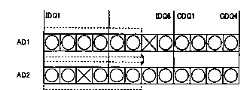
参照图10,在与行地址ROW-i对应的行的2个部位上存在不良存储单元。第1个部位是IO线IO-a上,第2个部位是IO线IO-b上。在这样的情况下,在现有的IO置换结构中,在只有1条备用IO线SIO的情况下,不能进行由IO置换得到的不良芯片的补救。Referring to FIG. 10, defective memory cells exist in two locations of the row corresponding to row address ROW-i. The first position is on the IO line IO-a, and the second position is on the IO line IO-b. In such a case, in the conventional IO replacement structure, when there is only one spare IO line SIO, it is impossible to remedy defective chips obtained by IO replacement.
但是,在实施例2中,如图9中所示,用不同的子字线驱动存储单元阵列的右半部分和左半部分,利用图8的SD发生电路204可变更一并驱动该子字线的单位。再有,关于SD发生电路204的结构,具有与图3、图4中已说明的SD发生电路4同样的结构,不重复进行说明。However, in
图11是说明实施例2中的存储单元的置换用的图。FIG. 11 is a diagram for explaining replacement of memory cells in the second embodiment.
参照图11,如果在存储单元阵列的右半部分和左半部分中对于由行地址ROW-i同时选择的存储单元的配置进行分配的变更,则也可补救图10中示出的不良。即,通过变更图3中示出的SD发生电路的开关电路92、96、100、104的设定,可变更地址的分配。Referring to FIG. 11 , the defect shown in FIG. 10 can also be remedied by changing the allocation of memory cells simultaneously selected by row address ROW-i in the right half and left half of the memory cell array. That is, by changing the settings of the
具体地说,在通常的情况下,与某个行地址ROW-i对应,一并地激活存储器区域ROW-i(L)、ROW-i(R)和备用存储单元SMCi。此外,对于另外的行地址ROW-j,一并地激活存储器区域ROW-j(L)、ROW-j(R)和备用存储单元SMCj。Specifically, normally, corresponding to a certain row address ROW-i, the memory regions ROW-i(L), ROW-i(R) and spare memory cell SMCi are collectively activated. Furthermore, for another row address ROW-j, the memory regions ROW-j(L), ROW-j(R) and the spare memory cell SMCj are collectively activated.
与此不同,在存储单元阵列的同一行的右半部分和左半部分中各存在1个合计2个不良存储单元的情况下,通过变更地址的分配,可补救这样的不良。On the other hand, when there is one defective memory cell in the right half and the left half of the same row of the memory cell array, a total of two defective memory cells can be corrected by changing the allocation of addresses.
具体地说,变更图8的SD发生电路204的内部设定,以便对于某个行地址ROW-i一并地激活存储器区域ROW-i(L)、ROW-j(R)和备用存储单元SMCj。而且,在图8的地址编程电路206中设定置换地址,以便将与存储器区域ROW-i(L)的IO线IOa相当的位置上存在的不良存储单元置换为备用存储单元SMCj即可。Specifically, the internal settings of the SD generating circuit 204 in FIG. 8 are changed so that the memory regions ROW-i(L), ROW-j(R) and the spare memory cell SMCj are simultaneously activated for a certain row address ROW-i. . In addition, in the address programming circuit 206 of FIG. 8, a replacement address may be set so that a defective memory cell existing at a position corresponding to the IO line 10a of the memory region ROW-i(L) is replaced with a spare memory cell SMCj.
此外,变更图8的SD发生电路204的内部设定,以便对于另外的行地址ROW-j一并地激活存储器区域ROW-j(L)、ROW-i(R)和备用存储单元SMCi。这时,在图8的地址编程电路206中设定置换地址,以便将与存储器区域ROW-i(R)中的IO线IOb相当的位置上存在的不良存储单元置换为备用存储单元SMCi即可。In addition, the internal setting of SD generating circuit 204 in FIG. 8 is changed so that memory regions ROW-j(L), ROW-i(R) and spare memory cell SMCi are activated collectively for another row address ROW-j. At this time, the replacement address is set in the address programming circuit 206 of FIG. 8 so that the defective memory cell existing at the position corresponding to the IO line 10b in the memory region ROW-i(R) may be replaced with the spare memory cell SMCi. .
而且,可通过变更图3中示出的SD发生电路中的开关电路92、96、100、104的设定来实现这样的地址的置换。例如,通过将开关电路100设定并变更为输出行地址信号/RA0、将开关电路104设定并变更为输出行地址信号RA0,可实现置换。Furthermore, such address replacement can be realized by changing the settings of the
如以上已说明的那样,在实施例2中,也能补救以往不能进行由置换得到的补救的在1个存储单元行的多个部位上存在不良存储单元的不良芯片。As described above, also in the second embodiment, it is possible to repair defective chips in which defective memory cells exist in a plurality of locations in one memory cell row, which conventionally cannot be repaired by replacement.
即,通过变更正规存储单元的地址分配,通过变更在正规存储单元上发生的不良存储单元的激活单位以使不良分散,可进行由备用存储单元导致的置换。由此,可使成品率提高。That is, by changing the address allocation of normal memory cells and by changing the activation unit of defective memory cells that occur in normal memory cells so that the defects are distributed, replacement by spare memory cells can be performed. Thereby, the yield can be improved.
〔实施例3〕[Example 3]
在实施例3中,与实施例2同样,涉及置换备用IO线的结构,但说明了从存储单元阵列到数据输入输出端子的路径的电路结构不同的情况。In the third embodiment, similar to the second embodiment, it relates to the configuration of replacing the spare IO line, but the case where the circuit configuration of the path from the memory cell array to the data input/output terminal is different is described.
图12是示出实施例3的半导体存储器301的结构的框图。FIG. 12 is a block diagram showing the structure of a semiconductor memory 301 of the third embodiment.
参照图12,半导体存储器301包含:地址编程电路306,存储进行由备用存储单元导致的置换的不良存储单元的地址;地址比较器308,将从外部输入的行地址信号RA和列地址信号CA与地址编程电路306的输出进行比较;IOS发生电路304,接受地址比较器308的输出,发生信号IOS1~IOS4;以及行译码器+列译码器302,接受行地址信号RA和列地址信号CA并对其进行译码。Referring to Fig. 12, semiconductor memory 301 comprises: address programming circuit 306, stores the address of the bad memory cell that carries out the replacement caused by spare memory cell; The output of the address programming circuit 306 is compared; the IOS generation circuit 304 receives the output of the address comparator 308 and generates signals IOS1 to IOS4; and the row decoder+column decoder 302 receives the row address signal RA and the column address signal CA and decode it.
半导体存储器301还包含:主字驱动器MWD,根据行译码器+列译码器302的输出来驱动主字线;以及存储单元阵列314,根据行译码器+列译码器302的输出进行选择工作。Semiconductor memory 301 also comprises: main word driver MWD, drives main word line according to the output of row decoder+column decoder 302; Choose work.
存储单元阵列314包含多个读出放大器带SAB和子字驱动器带SWD,由读出放大器带SAB和子字驱动器带SWD分割为多个存储器块。The
半导体存储器301还包含:2对1译码器,从由存储单元阵列输出数据的局部IO线LIO、/LIO和备用局部IO线SLIO、/SLIO中选择一半,与数据线IDQ1~IDQn和IDQs连接;以及数据线置换电路310,选择数据线IDQs来代替数据线IDQ1~IDQn中的某一条连接到端子上。The semiconductor memory 301 also includes: a 2-to-1 decoder, which selects half of the local IO lines LIO, /LIO and spare local IO lines SLIO, /SLIO outputting data from the memory cell array, and connects them to the data lines IDQ1-IDQn and IDQs ; and the data line replacement circuit 310 selects the data line IDQs to replace any one of the data lines IDQ1-IDQn to connect to the terminal.
数据线置换电路310包含将数据线IDQ1~IDQn置换为备用数据线IDQs用的开关SW1~SWn。The data line replacement circuit 310 includes switches SW1 to SWn for replacing the data lines IDQ1 to IDQn with spare data lines IDQs.
关于存储单元阵列314和行译码器+列译码器302的结构,由于与图9中已说明的存储单元阵列214和行译码器+列译码器202相同,故不重复进行说明。The structures of the
半导体存储器301利用行译码器+列译码器302、子字驱动器SWD、IOS发生电路304和2对1译码器309进行存储单元的行、列和局部IO线的选择作为第1阶段。此外,半导体存储器301利用地址编程电路306、地址比较器308和数据线置换电路310进行数据线的选择作为第2阶段。在该第2阶段的数据线的选择时,进行备用存储单元对于正规存储单元的置换。The semiconductor memory 301 utilizes the row decoder+column decoder 302, the subword driver SWD, the IOS generation circuit 304 and the 2-to-1
图13是示出图12中的2对1译码器309的结构的电路图。FIG. 13 is a circuit diagram showing the structure of the 2-to-1
参照图13,2对1译码器309包含:读放大器331,放大存储单元阵列314与对数据进行授受的局部IO线LIO1、/LIO1之间产生的电位差,输出给IO线IO-1;读放大器332,放大局部IO线LIO2、/LIO2之间产生的电位差,输出给IO线IO-2;读放大器333,放大局部IO线LIO3、/LIO3之间产生的电位差,输出给IO线IO-3;以及读放大器334,放大局部IO线LIO4、/LIO4之间产生的电位差,输出给IO线IO-4。Referring to FIG. 13 , the 2-to-1
2对1译码器309还包含:读放大器335,放大局部IO线LIO2n-1、/LIO2n-1之间产生的电位差,输出给IO线IO-(2n-1);读放大器336,放大局部IO线LIO2n、/LIO2n之间产生的电位差,输出给IO线IO-2n;读放大器337,放大备用局部IO线SLIO1、/SLIO1之间产生的电位差,输出给IO线SIO1;以及读放大器338,放大备用局部IO线SLIO2、/SLIO2之间产生的电位差,输出给IO线SIO2。The 2-to-1
2对1译码器309还包含分别接受信号IOS1、IOS2、IOS3、IOS4的缓冲电路320、322、340、342。The 2-to-1
2对1译码器3 09还包含:N沟道MOS晶体管324,连接在IO线IO-1与数据线IDQ1之间,在其栅上接受缓冲电路320的输出;N沟道MOS晶体管326,连接在IO线IO-2与数据线IDQ1之间,在其栅上接受缓冲电路322的输出;N沟道MOS晶体管328,连接在IO线IO-3与数据线IDQ2之间,在其栅上接受缓冲电路320的输出;以及N沟道MOS晶体管330,连接在IO线IO-4与数据线IDQ2之间,在其栅上接受缓冲电路322的输出。The 2-to-1
2对1译码器309还包含:N沟道MOS晶体管344,连接在IO线IO-(2n-1)与数据线IDQn之间,在其栅上接受缓冲电路340的输出;N沟道MOS晶体管346,连接在IO线IO-2n与数据线IDQn之间,在其栅上接受缓冲电路342的输出;N沟道MOS晶体管348,连接在备用IO线SIO1与数据线IDQs之间,在其栅上接受缓冲电路340的输出;以及N沟道MOS晶体管350,连接在备用IO线SIO2与数据线IDQs之间,在其栅上接受缓冲电路342的输出。2 to 1
图14是示出图12中的IOS发生电路304的结构的电路图。FIG. 14 is a circuit diagram showing the configuration of the IOS generation circuit 304 in FIG. 12 .
参照图14,IOS发生电路304包含:开关电路352,选择行地址信号RAx和作为其倒相信号的信号/RAx的某一方;AND电路354,接受开关电路352的输出和块选择信号BLK1,输出信号IOS1;以及AND电路358,接受开关电路356的输出和块选择信号BLK1,输出信号IOS2。Referring to Fig. 14, IOS generating circuit 304 comprises: switch circuit 352, selects a certain side of row address signal RAx and signal /RAx as its inverted signal; AND circuit 354, receives the output of switch circuit 352 and block select signal BLK1, outputs signal IOS1; and an AND circuit 358, which receives the output of the switch circuit 356 and the block selection signal BLK1, and outputs a signal IOS2.
IOS发生电路304还包含:开关电路360;AND电路362,接受开关电路360的输出和块选择信号BLK1,输出信号IOS3;开关电路364;AND电路366,接受开关电路364的输出和块选择信号BLK1,输出信号IOS4。IOS generating circuit 304 also includes: switch circuit 360; AND circuit 362, accepts the output of switch circuit 360 and block selection signal BLK1, output signal IOS3; switch circuit 364; AND circuit 366, accepts the output of switch circuit 364 and block selection signal BLK1 , output signal IOS4.
再有,块选择信号BLK1是激活在图12中示出的存储单元阵列314中被读出放大器带SAB区分的分割单位的信号。对行地址信号进行译码,从行译码器+列译码器302供给该块选择信号BLK1。虽然未图示,但是IOS发生电路304包含与由读出放大器带SAB导致的分割单位的数目同样的电路。而且,对IOS发生电路304输入了对应的块选择信号。In addition, the block selection signal BLK1 is a signal for activating the division unit divided by the sense amplifier band SAB in the
此外,由于开关电路352、356、360、364的结构与在图4中已说明的开关电路92的结构相同,故不重复进行说明。再有,如在图7中已说明的那样,也可使用与开关电路92A同样的结构,只在输入了对应的地址的情况下进行地址置换。In addition, since the structure of the switch circuits 352, 356, 360, 364 is the same as the structure of the
IOS发生电路304进行以下的第1、第2工作的某一工作。The IOS generating circuit 304 performs any one of the following first and second operations.
在第1工作中,IOS发生电路304与某个输入地址位RAx相对应,一并地选择图13的IO线IO-1、IO-3、IO线IO-(2n-1)和备用IO线SIO1,并且在使输入地址位RAx倒相的情况下,一并地选择图13的IO线IO-2、IO-4、IO线IO-2n和备用IO线SIO2。In the first work, the IOS generating circuit 304 corresponds to a certain input address bit RAx, and selects the IO lines IO-1, IO-3, IO lines IO-(2n-1) and the spare IO lines of FIG. 13 together. SIO1, and in the case of inverting the input address bit RAx, the IO lines IO-2, IO-4, IO line IO-2n and spare IO line SIO2 of FIG. 13 are selected together.
在第2工作中,IOS发生电路304与某个输入地址位RAx相对应,一并地选择图13的IO线IO-1、IO-3、IO线IO-2n和备用IO线SIO2,并且在使输入地址位RAx倒相的情况下,一并地选择图13的IO线IO-2、IO-4、IO线IO-(2n-1)和备用IO线SIO1。In the second work, the IOS generating circuit 304 corresponds to a certain input address bit RAx, selects the IO lines IO-1, IO-3, IO lines IO-2n and the spare IO line SIO2 of FIG. When inverting the input address bit RAx, the IO lines IO-2, IO-4, IO line IO-(2n-1) and spare IO line SIO1 of FIG. 13 are selected together.
根据在开关电路352、356、360、364中包含的熔断元件的设定来决定进行第1、第2工作的某一工作。According to the settings of the fuse elements included in the switch circuits 352 , 356 , 360 , and 364 , one of the first and second operations is determined.
图13的2对1译码器309根据IOS发生电路304输出的信号IOS1~IOS4进行数据线的选择工作。The 2-to-1
图15是说明在存储单元阵列的1个存储单元行中存在多个不良存储单元的情况用的图。FIG. 15 is a diagram for explaining a case where a plurality of defective memory cells exist in one memory cell row of the memory cell array.
在图15中,示出了在与行地址ROW-i对应的存储单元行上的2个部位上存在不良存储单元的情况。利用图13中已说明的2对1译码器309将第偶数条IO线和第奇数条IO线的某一条与数据线连接,对外部读出数据。在这样的结构的情况下,在不良存储单元存在的IO线IO-a和IO线IO-b都是偶数或奇数的情况下,即使对应的备用IO线是SIO1、SIO2这2条,在以往也不能进行补救。FIG. 15 shows a case where defective memory cells exist in two locations on the memory cell row corresponding to the row address ROW-i. Use the 2-to-1
但是,如在图13中已说明的那样,如果将2对1译码器309构成为在存储器阵列的右半部分和左半部分能分开地进行选择的转换,则能进行这样的不良芯片的补救。在进行补救时,对于存储器阵列的右半部分来说,如通常那样进行不良存储单元与备用存储单元的置换。另一方面,对于存储器阵列的左半部分来说,通过转换图14中示出的开关电路352、356的连接,可进行备用置换。However, as has been explained in FIG. 13, if the 2-to-1
图16是说明行地址的信号位RAx为0时的不良存储单元的置换用的图。FIG. 16 is a diagram for explaining replacement of defective memory cells when the row address signal bit RAx is 0. FIG.
参照图16,说明IO线IO-a、IO-b都是第偶数条的IO线的情况。对于包含IO线IO-a的阵列的左半部分来说,在行地址的信号位RAx为0时,将开关设定为选择第奇数条的IO线。Referring to FIG. 16 , the case where both the IO lines IO-a and IO-b are even-numbered IO lines will be described. For the left half of the array containing IO lines IO-a, when the signal bit RAx of the row address is 0, the switches are set to select the odd-numbered IO lines.
另一方面,对于包含IO线IO-b和备用IO线的阵列的右半部分来说,在行地址的信号位RAx为0时,将开关设定为选择第偶数条的IO线。通过这样做,不会同时进行2个不良存储单元的指定。On the other hand, for the right half of the array including the IO line IO-b and the spare IO line, when the signal bit RAx of the row address is 0, the switch is set to select the even-numbered IO line. By doing so, designation of two bad memory cells is not performed at the same time.
因而,在地址位RAx为0时,可置换并使用备用存储单元SMCR来代替IO线IO-b上的不良存储单元。Therefore, when the address bit RAx is 0, the spare memory cell SMCR can be replaced and used to replace the defective memory cell on the IO line IO-b.
图17是说明行地址的信号位RAx为1时的不良存储单元的置换用的图。FIG. 17 is a diagram for explaining replacement of defective memory cells when the row address signal bit RAx is 1. FIG.
参照图17,在行地址的信号位RAx为1时,将开关选择为在阵列的左半部分选择第偶数条的IO线。另一方面,对于阵列的右半部分来说,在行地址的信号位RAx为1时,将开关设定为选择第奇数条的IO线。通过这样来设定,可将IO线IO-a上的不良存储单元置换为备用存储单元SMCL来使用。Referring to FIG. 17 , when the signal bit RAx of the row address is 1, the switch is selected to select the even-numbered IO line in the left half of the array. On the other hand, for the right half of the array, when the signal bit RAx of the row address is 1, the switch is set to select the odd-numbered IO line. By setting in this way, the defective memory cell on the IO line IO-a can be used instead of the spare memory cell SMCL.
通过进行如在图16、图17中已说明的那样的置换,可使以往不能补救的不良芯片成为合格芯片。因而,即使在实施例3的半导体存储器中,与以往相比也能预期成品率的提高。By performing the replacement as described in FIGS. 16 and 17, defective chips that could not be repaired conventionally can be converted into good chips. Therefore, even in the semiconductor memory device of the third embodiment, improvement in yield can be expected compared with conventional ones.
〔实施例4〕[Example 4]
在实施例1~实施例3中,说明了通过变更存储单元阵列的右半部分和左半部分的地址分配提高了由备用存储单元得到的补救率的情况。In
但是,不限于分割1个存储单元阵列的情况,也有与1个行地址的输入相对应一并地激活处于分离的位置上的存储单元的情况。本发明也可应用于这样的情况。However, it is not limited to the case of dividing one memory cell array, and there may be a case of collectively activating memory cells at separate positions in response to input of one row address. The present invention is also applicable to such cases.
图18是示出实施例4的半导体存储器401的结构的概略框图。FIG. 18 is a schematic block diagram showing the structure of a
参照图18,半导体存储器401包含:多个存储体BANK#1~BANK#u;地址调换电路404,进行行地址信号RA、列地址信号CA的地址的与各存储体的对应关系的调换;地址编程电路406,存储不良存储单元的地址;以及IO选择器410,根据从比较被输入的行地址信号RA、列地址信号CA与地址编程电路406的输出而输出控制信号SELA的地址比较器408和地址调换电路404输出的控制信号SELB和从地址比较器408输出的控制信号SELA选择存储体BANK#1~BANK#u的输出,输出给数据端子。With reference to Fig. 18,
存储体BANK#1包含:行译码器+列译码器402#1,接受利用地址调换电路404进行了地址调换处理后的行地址和列地址;主字驱动器MWD#1;存储单元阵列414#1;以及2对1译码器409#1,进行存储单元阵列414#1与数据线IDQ1#1~IDQn#1和IDQs之间的数据授受。Memory
存储体BANK#2包含:行译码器+列译码器402#2,接受利用地址调换电路404进行了地址调换处理后的行地址和列地址;主字驱动器MWD#2;存储单元阵列414#2;以及2对1译码器409#2,进行存储单元阵列414#2与数据线IDQ1#2~IDQn#2之间的数据授受。Memory
存储体BANK#u包含:行译码器+列译码器402#u,接受利用地址调换电路404进行了地址调换处理后的行地址和列地址;主字驱动器MWD#u;存储单元阵列414#u;以及2对1译码器409#u,进行存储单元阵列414#u与数据线IDQ1#u~IDQn#u之间的数据授受。Memory bank BANK#u comprises: row decoder+
在此,如在图9中已说明的那样,在存储体BANK#1中设置了备用IO线和备用存储单元。另一方面,在存储体BANK#2~BANK#u中没有设置备用存储单元。在这样的情况下,半导体存储器401在存储体BANK#2~BANK#u的某一个中存在不良存储单元的情况下,可使用在存储体BANK#1中包含的备用存储单元进行置换。Here, as already described in FIG. 9 , spare IO lines and spare memory cells are provided in
图19是示出图18中的IO选择器410的结构的电路图。FIG. 19 is a circuit diagram showing the structure of the
参照图19,IO选择器410包含:IO置换电路412;2nDQ选择电路414;以及并串变换电路416。Referring to FIG. 19 , the
IO置换电路412包含多个开关418。在不良地址与输入地址一致的情况下,根据从地址比较器408输出的信号SELA进行存储单元的置换。开关418根据信号SELA,置换备用数据线IDQS与其它的数据线IDQ1#1~IDQn#1、数据线IDQ1#2~IDQn#2、...、数据线IDQ1#u~IDQn#u的某一条。The
2nDQ选择电路414根据从地址调换电路404输出的控制信号SELB,选择作为IO置换电路412的输出的u×n位的数据线中的2×n位输出。The
并串变换电路416对2×n位的数据进行并/串变换,成为n位后,输出信号DQ1~DQn。Parallel-
在图19中,说明了利用1个地址同时选择多个存储体中的2个存储体、进行2位预取后以来自存储体的读出频率的2倍的频率输出数据的情况。In FIG. 19 , a case where two banks out of a plurality of banks are simultaneously selected by one address, and data is output at a frequency twice the frequency of reading from the banks after performing 2-bit prefetching is described.
在这样的情况下,利用图18的地址调换电路404变更地址的分配,以便与包含备用存储单元的存储体同时激活包含不良存储单元的存储体。可使用与图3或图14中示出的结构同样的结构来实现地址调换电路404。In such a case, the allocation of addresses is changed by the
再有,不限于同时激活2个存储体的情况,即使在同时激活更多的存储体的情况下,利用地址调换,也能同样提高由备用存储单元得到的补救率。In addition, not only when two banks are activated simultaneously, but also when more banks are activated simultaneously, the recovery rate obtained from the spare memory cell can be similarly improved by address swapping.
如以上已说明的那样,在实施例4中,通过变更正规存储单元的地址的分配,可提高由备用存储单元得到的置换补救率,提高成品率。As described above, in the fourth embodiment, by changing the address allocation of the regular memory cells, the replacement recovery rate by the spare memory cells can be improved, and the yield can be improved.
〔实施例5〕[Example 5]
图20是示出实施例5的半导体存储器501的结构的框图。FIG. 20 is a block diagram showing the structure of a semiconductor memory 501 of the fifth embodiment.
参照图20,半导体存储器501包含:地址编程电路506,存储进行由备用存储单元导致的置换的不良存储单元的地址;地址比较器508,将从外部输入的行地址信号RA和列地址信号CA与地址编程电路506的输出进行比较;IOS发生电路504,接受地址比较器508的输出,发生信号IOS1~IOS4;以及行译码器+列译码器502,接受行地址信号RA和列地址信号CA并对其进行译码。Referring to FIG. 20, the semiconductor memory 501 includes: an address programming circuit 506, which stores the address of a defective memory cell replaced by a spare memory cell; The output of the address programming circuit 506 is compared; the IOS generation circuit 504 receives the output of the address comparator 508 and generates signals IOS1 to IOS4; and the row decoder+column decoder 502 receives the row address signal RA and the column address signal CA and decode it.
半导体存储器501还包含:主字驱动器MWD,根据行译码器+列译码器502的输出来驱动主字线;以及存储单元阵列514,根据行译码器+列译码器502的输出进行选择工作。Semiconductor memory 501 also includes: main word driver MWD, drives main word line according to the output of row decoder+column decoder 502; Choose work.
存储单元阵列514包含多个读出放大器带SAB和子字驱动器带SWD,由读出放大器带SAB和子字驱动器带SWD分割为多个存储器块。The memory cell array 514 includes a plurality of sense amplifier bands SAB and sub-word driver bands SWD, and is divided into a plurality of memory blocks by the sense amplifier bands SAB and sub-word driver bands SWD.
半导体存储器501还包含从由存储单元阵列输出数据的局部IO线LIO、/LIO和备用局部IO线SLIO、/SLIO中选择一半、与数据线IDQ1~IDQn和IDQs连接的2对1译码器509。The semiconductor memory 501 also includes a 2-to-1 decoder 509 that selects half of the local IO lines LIO, /LIO that output data from the memory cell array and the spare local IO lines SLIO, /SLIO, and is connected to the data lines IDQ1-IDQn and IDQs .
关于存储单元阵列514和行译码器+列译码器502的结构,由于与图9中已说明的存储单元阵列214和行译码器+列译码器202的结构相同,故不重复进行说明。由于IOS发生电路504的结构与图14中已说明的IOS发生电路304的结构相同,故不重复进行说明。此外,由于2对1译码器509也具有与图13中已说明的2对1译码器309同样的结构,故不重复进行说明。Regarding the structure of the memory cell array 514 and the row decoder+column decoder 502, since it is the same as the structure of the memory cell array 214 and the row decoder+column decoder 202 described in FIG. 9, it will not be repeated. illustrate. Since the structure of the IOS generating circuit 504 is the same as that of the IOS generating circuit 304 already described in FIG. 14, the description thereof will not be repeated. In addition, since the 2:1 decoder 509 also has the same configuration as the 2:1
半导体存储器501还包含根据地址比较器508的输出移动数据线IDQ1~IDQn和备用数据线IDQS与端子的连接的IO移动电路510。The semiconductor memory 501 further includes an
IO移动电路510在地址比较器508的输出显现出已被编程的不良存储单元的地址与输入地址一致的情况下,使用备用数据线IDQS。The
图21是示出图20中的IO移动电路510的结构的电路图。FIG. 21 is a circuit diagram showing the structure of the
参照图21,IO移动电路510包含分别与数据信号DQ1~DQn对应地设置的开关电路510.1~510.n。根据地址比较器508的输出进行开关电路510.1~510.n的连接转换。Referring to FIG. 21 , the
开关电路510.1连接数据线IDQ1、IDQ2的某一方与输出数据信号DQ1的端子。开关电路510.1在「没有移动」的情况下,连接数据线IDQ1与输出数据信号DQ1的端子,在「有移动」的情况下,连接数据线IDQ2与输出数据信号DQ1的端子。The switch circuit 510.1 connects one of the data lines IDQ1 and IDQ2 to a terminal that outputs the data signal DQ1. The switch circuit 510.1 connects the data line IDQ1 to the terminal of the output data signal DQ1 in the case of "no movement", and connects the data line IDQ2 to the terminal of the output data signal DQ1 in the case of "movement".
同样,其它的开关电路在「没有移动」的情况下,连接对应的编号的数据线与对应的编号的端子,在「有移动」的情况下,连接比对应的编号大1的编号的数据线与对应的编号的端子。但是,开关电路510.n在有移动的情况下,将备用数据线IDQs与输出数据信号DQn的端子连接。Similarly, other switching circuits connect the data line of the corresponding number to the terminal of the corresponding number in the case of "no movement", and connect the data line of the number greater than the corresponding number by 1 in the case of "movement". with corresponding numbered terminals. However, the switch circuit 510.n connects the backup data line IDQs to the terminal outputting the data signal DQn when there is movement.
在此,说明在数据线IDQ5中产生了缺陷的情况。在这样的情况下,将输出数据信号DQ1~DQ4的端子和对应的开关电路510.1~510.4定为「没有移动」的状态,对于与数据信号DQ5~DQn对应的开关电路510.5~510.n来说,定为「有移动」的状态。于是,也可不将数据线IDQ5连接到任一个端子上而不使用数据线IDQ5。Here, a case where a defect occurs in the data line IDQ5 will be described. In such a case, the terminals outputting the data signals DQ1-DQ4 and the corresponding switch circuits 510.1-510.4 are in the state of "no movement". For the switch circuits 510.5-510.n corresponding to the data signals DQ5-DQn , set the status as "moved". Therefore, the data line IDQ5 may not be used without connecting the data line IDQ5 to any terminal.
由这样的移动方式进行的置换的优点是可进行高速存取。即,如果经过图8的IO置换电路210那样的复杂的备用IO线的置换电路,则在与分离的IO线置换时,从备用IO线读出数据的路径变长。此外,附加在备用IO线上的寄生电容比其它的IO线上的寄生电容大。由移动方式进行的置换可克服这些弱点,减少了因置换引起的数据存取的延迟。An advantage of replacement by such a moving method is that high-speed access is possible. That is, if a complicated spare IO line replacement circuit such as the IO replacement circuit 210 in FIG. 8 is passed, the path for reading data from the spare IO line becomes longer when replacing with a separate IO line. In addition, the parasitic capacitance added to the standby IO line is larger than the parasitic capacitance of other IO lines. The replacement by moving can overcome these weaknesses and reduce the delay of data access caused by the replacement.
图22是说明在实施例5中能进行补救的不良存储单元的发生位置用的图。Fig. 22 is a diagram for explaining occurrence locations of defective memory cells that can be remedied in the fifth embodiment.
参照图22,说明在由行地址ROW-i指定的同一存储单元行中存在2个不良存储单元的情况。在该不良存储单元存在的IO线IO-a和IO-b都是第偶数条或第奇数条IO线的情况下,以往不能进行不良补救。Referring to FIG. 22, a case where two defective memory cells exist in the same memory cell row specified by the row address ROW-i will be described. If the IO lines IO-a and IO-b in which the defective memory cell exists are both even-numbered or odd-numbered IO lines, it has not been possible to remedy the defect conventionally.
但是,通过利用图20的IOS发生电路504来变更与2对1译码器509所选择的IO线的地址的对应关系,可进行与图16、图17中已说明的情况同样的置换。However, by changing the correspondence relationship with the address of the IO line selected by the 2:1 decoder 509 using the IOS generation circuit 504 of FIG. 20, the same replacement as that described in FIGS. 16 and 17 can be performed.
因而,在实施例5中,通过变更正规存储单元的地址的分配,也能提高使用了备用存储单元的不良补救率,也能谋求成品率的提高。Therefore, in Embodiment 5, by changing the address allocation of regular memory cells, it is possible to improve the defect recovery rate using spare memory cells, and also to improve the yield.
〔实施例6〕[Example 6]
在实施例6中,对于正规的存储单元相互的地址置换和由备用存储单元产生的不良存储单元的置换的组合来说,进一步将错误校正处理也组合进来了。In Embodiment 6, an error correction process is further incorporated into the combination of mutual address replacement of normal memory cells and replacement of defective memory cells by spare memory cells.
例如,对于具有芯片上的错误校正功能的半导体存储器来说,已在特开昭63-302497号公报和与其对应的美国专利4918692号公报中公开了。在具有芯片上的错误校正功能的半导体存储器中,对于存储单元阵列一并地输入输出数据组和冗余位。对于该数据组和冗余位组中发生的1位或多位的错误数据可自动地进行补救。该错误数据可起因于存储单元的不良,也可起因于由α线引起的软错误。For example, Japanese Unexamined Patent Application Publication No. 63-302497 and its corresponding US Patent No. 4,918,692 have disclosed a semiconductor memory having an on-chip error correction function. In a semiconductor memory having an on-chip error correction function, data sets and redundant bits are input and output together for a memory cell array. One or more erroneous data occurred in the data group and the redundant bit group can be automatically remedied. This erroneous data may be caused by a defect of a memory cell, or may be caused by a soft error caused by an α line.
具有这样的芯片上的错误校正功能的半导体存储器,由于必须多余地设置冗余位部分的存储单元,故在一并存储的数据的位数少的情况下,是不太经济的。A semiconductor memory having such an on-chip error correction function is not economical when the number of bits of data to be collectively stored is small because redundant memory cells must be provided.
但是,在如近年来的系统LSI那样内置DRAM的情况下,使内部数据总线宽度定为128位以上的情况也较多。这样,在一并存储的数据的位数多的情况下,减少了冗余位对于信息位的比率。因而,可较合适地使用具有这样的芯片上的错误校正功能的半导体存储器。However, when a DRAM is built-in like a recent system LSI, the internal data bus width is often set to 128 bits or more. In this way, when the number of bits of data to be collectively stored is large, the ratio of redundant bits to information bits is reduced. Therefore, a semiconductor memory having such an on-chip error correction function can be used more suitably.
图23是示出实施例6的半导体存储器601的结构的框图。FIG. 23 is a block diagram showing the structure of the semiconductor memory 601 of the sixth embodiment.
参照图23,半导体存储器601包含:地址编程电路606,存储进行由备用存储单元导致的置换的不良存储单元的地址;地址比较器608,将从外部输入的行地址信号RA和列地址信号CA与地址编程电路606的输出进行比较;IOS发生电路604,接受地址比较器608的输出,发生信号IOS1~IOS4;以及行译码器+列译码器602,接受行地址信号RA和列地址信号CA并对其进行译码。Referring to FIG. 23 , the semiconductor memory 601 includes: an address programming circuit 606, which stores the address of a defective memory cell that is replaced by a spare memory cell; The output of the address programming circuit 606 is compared; the IOS generation circuit 604 receives the output of the address comparator 608 and generates signals IOS1 to IOS4; and the row decoder+column decoder 602 receives the row address signal RA and the column address signal CA and decode it.
半导体存储器601还包含:主字驱动器MWD,根据行译码器+列译码器602的输出来驱动主字线;以及存储单元阵列614,根据行译码器+列译码器602的输出进行选择工作。Semiconductor memory 601 also includes: main word driver MWD, drives main word line according to the output of row decoder+column decoder 602; Choose work.
存储单元阵列614包含多个读出放大器带SAB和子字驱动器带SWD,由读出放大器带SAB和子字驱动器带SWD分割为多个存储器块。The memory cell array 614 includes a plurality of sense amplifier bands SAB and sub-word driver bands SWD, and is divided into a plurality of memory blocks by the sense amplifier bands SAB and sub-word driver bands SWD.
半导体存储器601还包含:2对1译码器609,从由存储单元阵列输出数据的局部IO线LIO、/LIO和备用局部IO线SLIO、/SLIO中选择一半、连接数据线IDQ1~IDQn与IDQs;以及数据线置换电路610。The semiconductor memory 601 also includes: a 2-to-1 decoder 609, which selects half of the local IO lines LIO, /LIO and spare local IO lines SLIO, /SLIO outputting data from the memory cell array, and connects the data lines IDQ1-IDQn and IDQs ; and the data line replacement circuit 610.
数据线置换电路610包含将数据线PDQ1~PDQn+m的某一个置换为备用数据线IDQs的多个开关。The data line replacement circuit 610 includes a plurality of switches for replacing any one of the data lines PDQ1 to PDQn+m with a spare data line IDQs.
数据线置换电路610在地址比较器608的输出显现出正被编程的不良存储单元的地址与输入地址一致的情况下,使用备用数据线IDQs。Data line replacement circuit 610 uses spare data line IDQs in the event that the output of address comparator 608 reveals that the address of the defective memory cell being programmed matches the input address.
关于存储单元阵列614和行译码器+列译码器602的结构,由于与图9中已说明的存储单元阵列214和行译码器+列译码器202的结构相同,故不重复进行说明。此外,由于2对1译码器609也具有与图13中已说明的2对1译码器309同样的结构,故不重复进行说明。Regarding the structure of the memory cell array 614 and the row decoder+column decoder 602, since it is the same as the structure of the memory cell array 214 and the row decoder+column decoder 202 that have been described in FIG. 9, it will not be repeated. illustrate. In addition, since the 2:1 decoder 609 also has the same configuration as the 2:1
半导体存储器601还包含ECC电路612。ECC电路612在从数据线置换电路610输出了数据组IDQ1~IDQn和冗余位组CDQ1~CDQm的情况下,据此进行错误校正,输出数据信号DQ1~DQn。另一方面,在从外部供给了数据信号DQ1~DQn的情况下,生成数据组IDQ1~IDQn和冗余位组CDQ1~CDQm,为了写入到存储单元阵列614中而输出。数据组IDQ1~IDQn和冗余位组CDQ1~CDQm的合计位数是错误校正用的单位位数。The semiconductor memory 601 also includes an ECC circuit 612 . When data groups IDQ1 to IDQn and redundancy byte groups CDQ1 to CDQm are output from data line replacement circuit 610 , ECC circuit 612 performs error correction based on them, and outputs data signals DQ1 to DQn. On the other hand, when data signals DQ1 to DQn are supplied from the outside, data groups IDQ1 to IDQn and redundant byte groups CDQ1 to CDQm are generated and output for writing into memory cell array 614 . The total number of bits of data groups IDQ1 to IDQn and redundant byte groups CDQ1 to CDQm is the unit number of bits for error correction.
图24是说明地址置换前的不良的位置用的图。Fig. 24 is a diagram for explaining defective positions before address replacement.
参照图24,在由地址AD1选择的地址图中,在数据位IDQ3和IDQ7上存在不良。在这样的情况下,在图23的ECC电路612只能进行1位的错误校正的情况下,不能进行不良芯片的补救。此外,如果是ECC电路612能进行2位的错误校正的情况,则可利用错误校正功能使不良芯片成为合格品,但在例如产生了由α线引起的软错误的情况下,不能预期利用ECC电路612进行错误校正。Referring to FIG. 24, in the address map selected by address AD1, there is a defect in data bits IDQ3 and IDQ7. In such a case, when the ECC circuit 612 in FIG. 23 can only perform 1-bit error correction, it is impossible to remedy defective chips. In addition, if the ECC circuit 612 can perform 2-bit error correction, it is possible to use the error correction function to make a defective chip into a good product. Circuitry 612 performs error correction.
在这样的情况下,如果能这样来进行分散,使得在由1个地址选择的部分中不存在多个不良,则在进行了不良芯片的补救的基础上,可利用ECC电路612对软错误进行错误校正。In such a case, if it can be distributed in such a way that there are not many defects in the part selected by one address, then the ECC circuit 612 can be used to correct the soft errors after remediating the defective chips. error correction.
图25是示出了能进行地址分配变更后的错误校正的不良的存在部位用的图。FIG. 25 is a diagram showing defective locations where error correction after address allocation change can be performed.
参照图25,用图23的IOS发生电路604进行将地址AD1的数据位IDQ1~IDQ6与地址AD2的数据位IDQ1~IDQ6进行调换那样的地址分配。通过这样做,如果是ECC电路612能进行1位的错误校正的情况,则能补救不良芯片。此外,如果是ECC电路612能进行2位的错误校正的情况,则可对1位为止的软错误进行错误校正。再者,在不良多时,预先进行地址编程电路606的编程,以便置换存储单元阵列中的备用存储单元即可。Referring to FIG. 25, the IOS generating circuit 604 of FIG. 23 performs address allocation such that data bits IDQ1-IDQ6 of address AD1 are swapped with data bits IDQ1-IDQ6 of address AD2. By doing so, if the ECC circuit 612 can perform 1-bit error correction, defective chips can be repaired. In addition, if the ECC circuit 612 can perform 2-bit error correction, it can perform error correction for up to 1-bit soft error. Furthermore, when there are many defects, programming of the address programming circuit 606 is performed in advance to replace spare memory cells in the memory cell array.
如上所述,可使以往不能补救的不良芯片成为合格芯片。此外,也可减少不良地址的编程中所需要的时间。因而,在实施例6的半导体存储器中,与以往相比,也可预期成品率的提高,同时也可预期因地址编程中所需要的时间缩短导致的制造成本的下降。As mentioned above, it is possible to turn defective chips that cannot be repaired in the past into good chips. In addition, the time required for programming of bad addresses can also be reduced. Therefore, in the semiconductor memory device of the sixth embodiment, an improvement in yield can be expected as compared with conventional ones, and a reduction in manufacturing cost due to shortening of the time required for address programming can also be expected.
〔实施例7〕[Example 7]
图26是示出实施例7的半导体存储器701的结构的电路图。FIG. 26 is a circuit diagram showing the structure of the
参照图26,半导体存储器701包含:地址编程电路706,存储进行由备用存储单元导致的置换的不良存储单元的地址;地址比较器708,将从外部输入的行地址信号RA和列地址信号CA与地址编程电路706的输出进行比较;IOS发生电路704,接受地址比较器708的输出,发生信号IOS1~IOS4;以及行译码器+列译码器702,接受行地址信号RA和列地址信号CA并对其进行译码。Referring to FIG. 26, the
半导体存储器701还包含:主字驱动器MWD,根据行译码器+列译码器702的输出来驱动主字线;以及存储单元阵列714,根据行译码器+列译码器702的输出进行选择工作。
存储单元阵列714包含多个读出放大器带SAB和子字驱动器带SWD,由读出放大器带SAB和子字驱动器带SWD分割为多个存储器块。The
半导体存储器701还包含从由存储单元阵列输出数据的局部IO线LIO、/LIO和备用局部IO线SLIO、/SLIO中选择一半、连接数据线IDQ1~IDQn与IDQs的2对1译码器709。The
关于存储单元阵列714和行译码器+列译码器702的结构,由于与图9中已说明的存储单元阵列214和行译码器+列译码器202的结构相同,故不重复进行说明。由于IOS发生电路704的结构与图14中已说明的IOS发生电路304的结构相同,故不重复进行说明。此外,由于2对1译码器709也具有与图13中已说明的2对1译码器309同样的结构,故不重复进行说明。Regarding the structure of the
半导体存储器701还包含根据地址比较器708的输出移动数据线IDQ1~IDQn和备用数据线IDQs与端子的连接的IO移动电路710。The
IO移动电路710在地址比较器708的输出显现出正被编程的不良存储单元的地址与输入地址一致的情况下,使用备用数据线IDQS。The
半导体存储器701还包含ECC电路712。ECC电路712在从IO移动电路710输出了数据组IDQ1~IDQn和冗余位组CDQ1~CDQm的情况下,据此进行错误校正,输出数据信号DQ1~DQn。另一方面,在从外部供给了数据信号DQ1~DQn的情况下,生成数据组IDQ1~IDQn和冗余位组CDQ1~CDQm,为了写入到存储单元阵列714中而输出。The
如图26中所示,通过将IO移动电路710和ECC电路712组合起来,与实施例6的情况相比,可进一步谋求存取速度的改善。As shown in FIG. 26, by combining the
〔实施例8〕[Example 8]
在实施例1~实施例7中,根据存储单元阵列中的不良存储单元的存在状况,变更从外部供给的地址与内部的存储单元阵列的物理的位置的关系。在以这种方式进行地址变更的情况下,存在如果在测试时没有掌握地址与存储单元的对应关系则不能进行正确的测试的问题。实施例8的发明就是为了解决这样的问题的发明。In
图27是示出了在实施例8的半导体存储器中代替图4中示出的开关电路92而使用的开关电路802的结构的电路图。FIG. 27 is a circuit diagram showing a configuration of a
参照图27,开关电路802包含:熔断元件812,连接在电源节点与节点N1之间;电阻814,连接在节点N1与接地节点之间;倒相器816,其输入端连接到节点N1上;N沟道MOS晶体管818,连接在输入节点IN1与输出节点OUT之间,其栅连接到节点N1上;以及N沟道MOS晶体管820,连接在输入节点IN2与输出节点OUT之间,其栅上接受倒相器816的输出。Referring to FIG. 27, the
开关电路802还包含连接在电源节点与节点N1之间、在栅上接受测试信号/TEST1的P沟道MOS晶体管822。The
其次,说明开关电路802的工作。Next, the operation of the
在通常时,通过切断熔断元件812进行正规存储单元相互的地址置换。此时,将测试信号/TEST1设定为高电平,如果熔断元件812被切断,则将节点N1设定为低电平,进行地址的置换。Normally, by cutting off the
另一方面,在测试模式时,将测试信号/TEST1设定为低电平,P沟道MOS晶体管822导通,即使在熔断元件812被切断的情况下,节点N1也被设定为默认状态的高电平。On the other hand, in the test mode, the test signal /TEST1 is set to a low level, the P-
如以上已说明的那样,通过设置开关电路802,由于即使在进行了地址置换后也能在测试模式中返回到初始的默认状态,故在测试时可进行正确的测试,在进行不良芯片的分析的情况下也可指定不良存储单元的准确的位置。As explained above, by setting the
图28是说明第2测试模式用的图。Fig. 28 is a diagram for explaining the second test mode.
参照图28,为了将图4中已说明的开关电路92的节点N1的电位输出给外部,设置三态倒相器832和端子842。三态倒相器832包含在电源节点与接地节点之间串联地连接的P沟道MOS晶体管834、836和N沟道MOS晶体管838、840。Referring to FIG. 28, a
P沟道MOS晶体管834在栅上接受测试信号/TEST2。P沟道MOS晶体管836、N沟道MOS晶体管838的栅都连接到节点N1上。N沟道MOS晶体管840在栅上接受测试信号TEST2。P沟道MOS晶体管836的漏连接到端子842上。P-
如果在测试模式中将测试信号TEST2设定为高电平、将测试信号/TEST2设定为低电平,则节点N1的电位的倒相信号从端子842作为信号EXOUT被输出。通过观察信号EXOUT,可观察在开关电路92中是否设定了地址置换。由此,可在之后在外部掌握地址编程状态。In the test mode, when the test signal TEST2 is set to a high level and the test signal /TEST2 is set to a low level, an inversion signal of the potential of the node N1 is output from the terminal 842 as a signal EXOUT. Whether or not address replacement is set in the
图29是说明组合了图27、图28的变例用的图。Fig. 29 is a diagram for explaining a modification in which Figs. 27 and 28 are combined.
参照图29,示出了组合了在测试模式中可将设定返回到默认状态的开关电路802和在测试模式中能将开关电路802的选择信息输出给外部的三态倒相器832的状态。如果这样做,则在将测试信号/TEST1设定为低电平的第1测试模式中,可将地址编程部分返回到初始状态,而且,在第2测试模式中,可从外部端子842监视开关电路802的选择状态。Referring to FIG. 29 , it shows a combination of a
通过设置以上那样的测试模式,可从外部使进行了正规存储单元相互的地址置换的编程状态返回到原来的状态。或者,可从外部监视地址置换的设定状态。因而,可进行将外部输入地址与内部存储单元阵列的物理位置对应起来的测试。By setting the test mode as described above, it is possible to return to the original state the programmed state in which the addresses of normal memory cells have been exchanged between each other from the outside. Alternatively, the setting status of address replacement can be monitored externally. Thus, a test for associating an externally input address with a physical location of the internal memory cell array can be performed.
以上,参照附图详细地说明了本发明,但这些说明始终是例示性的,而不是在任何意义上来限定本发明,本发明的要旨和范围只由后附的权利要求书来限定,包含与权利要求的范围均等的意义和范围内的全部的变更。Above, the present invention has been described in detail with reference to the accompanying drawings, but these descriptions are illustrative all the way, rather than limit the present invention in any sense, the gist and scope of the present invention are only limited by the appended claims, including and All modifications within the equal meaning and scope of the claims are intended.
Claims (10)
Applications Claiming Priority (3)
| Application Number | Priority Date | Filing Date | Title |
|---|---|---|---|
| JP194597/02 | 2002-07-03 | ||
| JP194597/2002 | 2002-07-03 | ||
| JP2002194597AJP4111762B2 (en) | 2002-07-03 | 2002-07-03 | Semiconductor memory device |
Publications (2)
| Publication Number | Publication Date |
|---|---|
| CN1467746Atrue CN1467746A (en) | 2004-01-14 |
| CN100538879C CN100538879C (en) | 2009-09-09 |
Family
ID=29997015
Family Applications (1)
| Application Number | Title | Priority Date | Filing Date |
|---|---|---|---|
| CNB031205143AExpired - Fee RelatedCN100538879C (en) | 2002-07-03 | 2003-03-13 | The semiconductor memory that the rate of remedying of bad chip has improved |
Country Status (3)
| Country | Link |
|---|---|
| US (1) | US6813199B2 (en) |
| JP (1) | JP4111762B2 (en) |
| CN (1) | CN100538879C (en) |
Cited By (8)
| Publication number | Priority date | Publication date | Assignee | Title |
|---|---|---|---|---|
| CN112908402A (en)* | 2021-03-31 | 2021-06-04 | 长鑫存储技术有限公司 | Spare circuit allocation method, device, equipment and medium |
| US11791010B2 (en) | 2020-08-18 | 2023-10-17 | Changxin Memory Technologies, Inc. | Method and device for fail bit repairing |
| US11791012B2 (en) | 2021-03-31 | 2023-10-17 | Changxin Memory Technologies, Inc. | Standby circuit dispatch method, apparatus, device and medium |
| US11797371B2 (en) | 2020-08-18 | 2023-10-24 | Changxin Memory Technologies, Inc. | Method and device for determining fail bit repair scheme |
| US11853152B2 (en) | 2020-08-18 | 2023-12-26 | Changxin Memory Technologies, Inc. | Fail bit repair method and device |
| US11881278B2 (en) | 2021-03-31 | 2024-01-23 | Changxin Memory Technologies, Inc. | Redundant circuit assigning method and device, apparatus and medium |
| US11887685B2 (en) | 2020-08-18 | 2024-01-30 | Changxin Memory Technologies, Inc. | Fail Bit repair method and device |
| US11984179B2 (en) | 2021-03-26 | 2024-05-14 | Changxin Memory Technologies, Inc. | Redundant circuit assigning method and device, and medium |
Families Citing this family (19)
| Publication number | Priority date | Publication date | Assignee | Title |
|---|---|---|---|---|
| KR100463198B1 (en)* | 2002-02-05 | 2004-12-23 | 삼성전자주식회사 | Semiconductor memory device with a data line redundancy scheme |
| US7505321B2 (en) | 2002-12-31 | 2009-03-17 | Sandisk 3D Llc | Programmable memory array structure incorporating series-connected transistor strings and methods for fabrication and operation of same |
| US7233024B2 (en)* | 2003-03-31 | 2007-06-19 | Sandisk 3D Llc | Three-dimensional memory device incorporating segmented bit line memory array |
| WO2005006345A1 (en)* | 2003-07-15 | 2005-01-20 | Elpida Memory, Inc. | Semiconductor storage device |
| US7221588B2 (en) | 2003-12-05 | 2007-05-22 | Sandisk 3D Llc | Memory array incorporating memory cells arranged in NAND strings |
| EP1717814B1 (en)* | 2004-02-20 | 2012-09-19 | Spansion LLc | Semiconductor storage device and semiconductor storage device control method |
| US7142471B2 (en)* | 2005-03-31 | 2006-11-28 | Sandisk 3D Llc | Method and apparatus for incorporating block redundancy in a memory array |
| JP2007257791A (en)* | 2006-03-24 | 2007-10-04 | Fujitsu Ltd | Semiconductor memory device |
| US7548459B2 (en)* | 2006-08-29 | 2009-06-16 | Micron Technology, Inc. | Method, apparatus, and system providing adjustable memory page configuration |
| JP2008108297A (en)* | 2006-10-23 | 2008-05-08 | Toshiba Corp | Nonvolatile semiconductor memory device |
| KR20090087077A (en)* | 2006-11-21 | 2009-08-14 | 프리스케일 세미컨덕터, 인크. | Memory system with ECC unit and additional processing unit |
| KR100850283B1 (en)* | 2007-01-25 | 2008-08-04 | 삼성전자주식회사 | Resistive semiconductor memory device having three dimension stack structure and method for word line decoding the same |
| JP4820795B2 (en)* | 2007-10-04 | 2011-11-24 | パナソニック株式会社 | Semiconductor memory device |
| JP5451971B2 (en)* | 2007-11-09 | 2014-03-26 | スパンション エルエルシー | Semiconductor device and control method thereof |
| CN107408408B (en)* | 2015-03-10 | 2021-03-05 | 美光科技公司 | Apparatus and method for shift determination |
| KR102435181B1 (en) | 2015-11-16 | 2022-08-23 | 삼성전자주식회사 | Semiconductor memory device, memory system including the same and method of operating memory system |
| US10725933B2 (en)* | 2016-12-30 | 2020-07-28 | Intel Corporation | Method and apparatus for redirecting memory access commands sent to unusable memory partitions |
| KR102697631B1 (en) | 2019-10-28 | 2024-08-23 | 삼성전자주식회사 | Memory device varying repair unit and repair method thereof |
| CN116072168B (en)* | 2021-10-29 | 2025-08-29 | 长鑫存储技术有限公司 | Memory structure and memory |
Family Cites Families (9)
| Publication number | Priority date | Publication date | Assignee | Title |
|---|---|---|---|---|
| JPH071640B2 (en) | 1987-06-03 | 1995-01-11 | 三菱電機株式会社 | Defect relief device for semiconductor memory device |
| JP2882369B2 (en)* | 1996-06-27 | 1999-04-12 | 日本電気株式会社 | Semiconductor storage device |
| JP3206541B2 (en)* | 1998-03-04 | 2001-09-10 | 日本電気株式会社 | Semiconductor storage device |
| JP3749789B2 (en)* | 1998-06-08 | 2006-03-01 | 株式会社東芝 | Semiconductor memory device |
| JP2001052495A (en)* | 1999-06-03 | 2001-02-23 | Toshiba Corp | Semiconductor memory |
| JP4001263B2 (en) | 2000-05-26 | 2007-10-31 | 株式会社ルネサステクノロジ | Semiconductor device |
| JP3821637B2 (en)* | 2000-08-24 | 2006-09-13 | 株式会社東芝 | Semiconductor integrated circuit device |
| TW546664B (en)* | 2001-01-17 | 2003-08-11 | Toshiba Corp | Semiconductor storage device formed to optimize test technique and redundancy technology |
| US6594177B2 (en)* | 2001-08-02 | 2003-07-15 | Stmicroelectronics, Inc. | Redundancy circuit and method for replacing defective memory cells in a flash memory device |
- 2002
- 2002-07-03JPJP2002194597Apatent/JP4111762B2/ennot_activeExpired - Fee Related
- 2002-12-30USUS10/330,071patent/US6813199B2/ennot_activeExpired - Fee Related
- 2003
- 2003-03-13CNCNB031205143Apatent/CN100538879C/ennot_activeExpired - Fee Related
Cited By (9)
| Publication number | Priority date | Publication date | Assignee | Title |
|---|---|---|---|---|
| US11791010B2 (en) | 2020-08-18 | 2023-10-17 | Changxin Memory Technologies, Inc. | Method and device for fail bit repairing |
| US11797371B2 (en) | 2020-08-18 | 2023-10-24 | Changxin Memory Technologies, Inc. | Method and device for determining fail bit repair scheme |
| US11853152B2 (en) | 2020-08-18 | 2023-12-26 | Changxin Memory Technologies, Inc. | Fail bit repair method and device |
| US11887685B2 (en) | 2020-08-18 | 2024-01-30 | Changxin Memory Technologies, Inc. | Fail Bit repair method and device |
| US11984179B2 (en) | 2021-03-26 | 2024-05-14 | Changxin Memory Technologies, Inc. | Redundant circuit assigning method and device, and medium |
| CN112908402A (en)* | 2021-03-31 | 2021-06-04 | 长鑫存储技术有限公司 | Spare circuit allocation method, device, equipment and medium |
| CN112908402B (en)* | 2021-03-31 | 2022-05-10 | 长鑫存储技术有限公司 | Spare circuit allocation method, device, equipment and medium |
| US11791012B2 (en) | 2021-03-31 | 2023-10-17 | Changxin Memory Technologies, Inc. | Standby circuit dispatch method, apparatus, device and medium |
| US11881278B2 (en) | 2021-03-31 | 2024-01-23 | Changxin Memory Technologies, Inc. | Redundant circuit assigning method and device, apparatus and medium |
Also Published As
| Publication number | Publication date |
|---|---|
| JP2004039098A (en) | 2004-02-05 |
| CN100538879C (en) | 2009-09-09 |
| US20040004866A1 (en) | 2004-01-08 |
| JP4111762B2 (en) | 2008-07-02 |
| US6813199B2 (en) | 2004-11-02 |
Similar Documents
| Publication | Publication Date | Title |
|---|---|---|
| CN1467746A (en) | Semiconductor memory with improved recovery rate of defective chips | |
| CN1249725C (en) | Semiconductor storage formed for optimizing testing technique and rebundance technique | |
| CN1168097C (en) | Semiconductor device having test circuit capable of suppressing increase in circuit scale | |
| CN1096083C (en) | Semi-conductor memory device | |
| CN1365148A (en) | Semiconductor storage device with tediously long system | |
| CN100338681C (en) | Thin film magnetic memory device having redundant configuration | |
| CN1134017C (en) | Semiconductor device having semiconductor memory circuit to be tested, method of testing semiconductor memory circuit and head circuit for semiconductor memory circuit | |
| CN1199275C (en) | semiconductor memory | |
| CN1416574A (en) | Semiconductor memory | |
| CN1191585C (en) | Self-analyzing semiconductor IC unit capable of carrying out redundant replacement with installed memory circuits | |
| CN1274161A (en) | semiconductor storage device | |
| CN1252727C (en) | Thin film magnetic memory device including memory cells with magnetic tunnel junctions | |
| CN1255817C (en) | Semiconductor integrated circuit comprising storage macro | |
| CN1136583C (en) | Semiconductor memory device | |
| CN1428788A (en) | Semiconductor memory | |
| CN1905074A (en) | Semiconductor memory device | |
| CN1477645A (en) | Nonvolatile semiconductor memory with increased probability of redundant recovery | |
| CN1823392A (en) | Semiconductor storage device | |
| CN100338774C (en) | Semiconductor memory | |
| CN1892891A (en) | Semiconductor memory | |
| CN1825488A (en) | Multiple-time programmable semiconductor storage device and multiple-time programming method thereof | |
| CN1203487C (en) | Redundant circuit of semicnductor memory | |
| CN1158666C (en) | Semiconductor memory device | |
| CN1913156A (en) | semiconductor integrated circuit | |
| CN1421870A (en) | Semiconductor storage device |
Legal Events
| Date | Code | Title | Description |
|---|---|---|---|
| C06 | Publication | ||
| PB01 | Publication | ||
| C10 | Entry into substantive examination | ||
| SE01 | Entry into force of request for substantive examination | ||
| C14 | Grant of patent or utility model | ||
| GR01 | Patent grant | ||
| C17 | Cessation of patent right | ||
| CF01 | Termination of patent right due to non-payment of annual fee | Granted publication date:20090909 Termination date:20140313 |