CN1453762A - Efficient liquid crystal display drive voltage generating circuit and its method - Google Patents
Efficient liquid crystal display drive voltage generating circuit and its methodDownload PDFInfo
- Publication number
- CN1453762A CN1453762ACN03106712ACN03106712ACN1453762ACN 1453762 ACN1453762 ACN 1453762ACN 03106712 ACN03106712 ACN 03106712ACN 03106712 ACN03106712 ACN 03106712ACN 1453762 ACN1453762 ACN 1453762A
- Authority
- CN
- China
- Prior art keywords
- voltage
- driving voltage
- clock signal
- driving
- frequency
- Prior art date
- Legal status (The legal status is an assumption and is not a legal conclusion. Google has not performed a legal analysis and makes no representation as to the accuracy of the status listed.)
- Granted
Links
Images


Classifications
- G—PHYSICS
- G09—EDUCATION; CRYPTOGRAPHY; DISPLAY; ADVERTISING; SEALS
- G09G—ARRANGEMENTS OR CIRCUITS FOR CONTROL OF INDICATING DEVICES USING STATIC MEANS TO PRESENT VARIABLE INFORMATION
- G09G3/00—Control arrangements or circuits, of interest only in connection with visual indicators other than cathode-ray tubes
- G09G3/20—Control arrangements or circuits, of interest only in connection with visual indicators other than cathode-ray tubes for presentation of an assembly of a number of characters, e.g. a page, by composing the assembly by combination of individual elements arranged in a matrix no fixed position being assigned to or needed to be assigned to the individual characters or partial characters
- G09G3/34—Control arrangements or circuits, of interest only in connection with visual indicators other than cathode-ray tubes for presentation of an assembly of a number of characters, e.g. a page, by composing the assembly by combination of individual elements arranged in a matrix no fixed position being assigned to or needed to be assigned to the individual characters or partial characters by control of light from an independent source
- G09G3/36—Control arrangements or circuits, of interest only in connection with visual indicators other than cathode-ray tubes for presentation of an assembly of a number of characters, e.g. a page, by composing the assembly by combination of individual elements arranged in a matrix no fixed position being assigned to or needed to be assigned to the individual characters or partial characters by control of light from an independent source using liquid crystals
- G09G3/3611—Control of matrices with row and column drivers
- G09G3/3696—Generation of voltages supplied to electrode drivers
- G—PHYSICS
- G09—EDUCATION; CRYPTOGRAPHY; DISPLAY; ADVERTISING; SEALS
- G09G—ARRANGEMENTS OR CIRCUITS FOR CONTROL OF INDICATING DEVICES USING STATIC MEANS TO PRESENT VARIABLE INFORMATION
- G09G2330/00—Aspects of power supply; Aspects of display protection and defect management
- G09G2330/02—Details of power systems and of start or stop of display operation
Landscapes
- Engineering & Computer Science (AREA)
- Chemical & Material Sciences (AREA)
- Crystallography & Structural Chemistry (AREA)
- Physics & Mathematics (AREA)
- Computer Hardware Design (AREA)
- General Physics & Mathematics (AREA)
- Theoretical Computer Science (AREA)
- Dc-Dc Converters (AREA)
- Liquid Crystal Display Device Control (AREA)
- Control Of Indicators Other Than Cathode Ray Tubes (AREA)
- Transforming Electric Information Into Light Information (AREA)
- Liquid Crystal (AREA)
Abstract
Translated fromChinese
Description
Translated fromChinese技术领域technical field
本发明涉及一种驱动液晶显示器(LCD)用的集成电路,具体涉及用于产生LCD驱动集成电路(称之为LCD驱动器IC)中的驱动电压的电路。The invention relates to an integrated circuit for driving a liquid crystal display (LCD), in particular to a circuit for generating a driving voltage in an LCD driving integrated circuit (called an LCD driver IC).
背景技术Background technique
LCD是手提式电脑和个人数字助理之类的便携式通信装置或者家用电器中使用的显示装置。LCD利用了透光率会根据施加在液晶板两端的电压值而变化的原理来显示数据。现在一般有两类LCD,即STN(超扭转向列)-LCD和TFT(薄膜晶体管)-LCD。驱动这些LCD的方法是不同的。LCDs are display devices used in portable communication devices such as laptop computers and personal digital assistants, or home appliances. LCDs display data using the principle that light transmittance changes according to the voltage value applied across the liquid crystal panel. Now generally there are two types of LCDs, namely STN (Super Twisted Nematic)-LCD and TFT (Thin Film Transistor)-LCD. The methods of driving these LCDs are different.
LCD驱动器IC是用于产生在LCD液晶板上显示数据所需的驱动电压的IC。一般来说,在液晶板两端都有可施加电压的电极。位于液晶板一端的电极被称为公共电极,而位于液晶板另一端的电极被称为线段电极。输入到公共电极的电压被称为公共电压,而输入到线段电极的电压被称为线段电压。An LCD driver IC is an IC that generates the driving voltage required to display data on the LCD liquid crystal panel. Generally, there are electrodes at both ends of the liquid crystal panel to which a voltage can be applied. The electrodes at one end of the liquid crystal panel are called common electrodes, and the electrodes at the other end of the liquid crystal panel are called line segment electrodes. The voltage input to the common electrode is referred to as the common voltage, and the voltage input to the segment electrodes is referred to as the segment voltage.
LCD驱动器IC被设计成能接收要在LCD上显示的字符或图象,将字符或图象的数据切换成线段电压和公共电压,然后将切换后的电压施加到液晶板上显示。The LCD driver IC is designed to receive characters or images to be displayed on the LCD, switch the data of the characters or images into line segment voltages and common voltages, and then apply the switched voltages to the LCD panel for display.
一般来说,会有六个电平的驱动电压输入LCD板的公共电极和线段电极。由驱动电压发生电路产生这六个电平的驱动电压。重要的是以高效、低能耗产生驱动电压。Generally, there are six levels of driving voltage input to the common electrode and line segment electrodes of the LCD panel. These six levels of driving voltages are generated by the driving voltage generating circuit. It is important to generate the driving voltage with high efficiency and low power consumption.
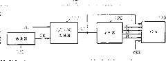
图1是表示现有LCD驱动器IC的驱动电压发生电路的方框图。图1中的电路是用于传统STN-LCD驱动器IC的电路。传统的LCD驱动电压发生电路100包括:DC-DC变换器110,分压器120和振荡器130。DC-DC变换器110是被称为增压器(booster)的电路,它通过将接收的输入电压VCI放大预定量而产生第一驱动电压V0。第一驱动电压V0是驱动LCD板140所需的高电压。FIG. 1 is a block diagram showing a driving voltage generating circuit of a conventional LCD driver IC. The circuit in Figure 1 is the one used in a conventional STN-LCD driver IC. A conventional LCD driving
DC-DC变换器110基本上通过切换和借助电荷的注入(pumping)为电容器充入电荷来实现增压。将一定周期的时钟信号CK用作进行切换所需的切换信号。该时钟信号CK在振荡器130中产生。由分压器120对DC-DC变换器110产生的第一驱动电压V0进行分压,然后将其作为第二到第五驱动电压V1-V4输出。The DC-
在驱动LCD板140时,板中的能量或电流消耗根据显示模式而变化,于是第一驱动电压V0的电平也改变。换句话说,如果板的电流消耗很低,就能维持第一驱动电压V0的电平。但是,如果板的电流消耗很高,就能使第一驱动电压V0的电平降低很多。When driving the LCD panel 140, energy or current consumption in the panel varies according to the display mode, and thus the level of the first driving voltage V0 also varies. In other words, if the current consumption of the panel is low, the level of the first driving voltage V0 can be maintained. However, if the current consumption of the board is high, the level of the first driving voltage V0 can be lowered considerably.
正如上面所述,如果电流消耗根据显示模式而变化,并且第一驱动电压V0的电平也根据电流消耗而变化,那么显示器的亮度也将根据显示模式而变化。由于第二到第五驱动电压V1-V4是基于第一驱动电压V0产生的,因此重要的是将第一驱动电压V0增压到某一电平。As described above, if the current consumption varies according to the display mode, and the level of the first driving voltage V0 also varies according to the current consumption, the brightness of the display will also vary according to the display mode. Since the second to fifth driving voltages V1-V4 are generated based on the first driving voltage V0, it is important to boost the first driving voltage V0 to a certain level.
但是,如果DC-DC变换器110利用了频率固定的时钟信号CK,就象利用了图1所示的传统驱动电压发生电路100的情况那样,此时就不能有效增压。增压器的效率受功率消耗和增压效率影响。即,优选的是利用能耗低、增压效率高的DC-DC变换器。However, if the DC-
要注意的是,将增压效率、即第一驱动电压V0的目标值与第一驱动电压V0的比值表示为百分比。即,如果第一驱动电压的目标值是10V,而第一驱动电压V0的电平降到8V,那么增压效率就是80%。因此,不管LCD板140的负荷如何,都需要将第一驱动电压V0维持在预定电平,以提高增压效率。It should be noted that the boosting efficiency, that is, the ratio of the target value of the first driving voltage V0 to the first driving voltage V0 is expressed as a percentage. That is, if the target value of the first driving voltage is 10V, and the level of the first driving voltage V0 is lowered to 8V, the boosting efficiency is 80%. Therefore, regardless of the load of the LCD panel 140, it is necessary to maintain the first driving voltage V0 at a predetermined level to improve boosting efficiency.
通常来说,如果LCD板140的电流消耗很低,就可以利用极低频率的时钟信号CK获得足够的增压效率。另一方面,随着LCD板140的电流消耗增大,需要增加时钟信号CK的频率来提高增压效率。Generally speaking, if the current consumption of the LCD panel 140 is very low, sufficient boosting efficiency can be obtained by using a very low frequency clock signal CK. On the other hand, as the current consumption of the LCD panel 140 increases, the frequency of the clock signal CK needs to be increased to improve boosting efficiency.
但是,传统驱动电压发生电路100都使用频率固定的时钟信号。如果LCD板140的电流消耗很低,DC-DC变换器100就会无谓地消耗电流。一般,如果时钟信号CK的频率很高,被DC-DC变换器110占用的电流也会增大。However, the conventional driving
另一方面,如果LCD板140的电流消耗非常高,就需要频率相对高的时钟信号CK。但是,传统的驱动电压发生电路100是利用频率固定的时钟信号进行增压,这就降低了第一驱动电压V0的电平。因此,显示质量也下降。On the other hand, if the current consumption of the LCD panel 140 is very high, a relatively high frequency clock signal CK is required. However, the conventional driving
发明内容Contents of the invention
本发明的目的是提供一种LCD驱动电压发生电路,其中通过降低功率消耗、改进增压效率,从而不管LCD板的电流消耗增加与否,显示质量都不会下降。It is an object of the present invention to provide an LCD drive voltage generating circuit in which by reducing power consumption and improving boosting efficiency, the display quality will not deteriorate regardless of an increase in current consumption of the LCD panel.
本发明的另一目的是提供一种产生施加给LCD驱动电压发生电路的LCD驱动电压的方法。Another object of the present invention is to provide a method of generating an LCD driving voltage applied to an LCD driving voltage generating circuit.
为了实现本发明的第一目的,提供了一种液晶显示器(LCD)驱动电压发生电路。该电路包括DC-DC变换器,用以响应时钟信号对输入电压进行增压,从而提供增压电压,并将增压电压作为第一驱动电压输出。压控振荡器产生一频率响应控制电压的电平而变化的时钟信号。控制电压发生器响应参考电压与由第一驱动电压派生的反馈电压之差,产生控制电压。In order to achieve the first object of the present invention, a liquid crystal display (LCD) driving voltage generating circuit is provided. The circuit includes a DC-DC converter, which is used to boost the input voltage in response to the clock signal, so as to provide a boosted voltage, and output the boosted voltage as the first driving voltage. The voltage controlled oscillator generates a clock signal whose frequency varies in response to the level of the control voltage. A control voltage generator generates a control voltage in response to a difference between the reference voltage and a feedback voltage derived from the first drive voltage.
在一个实施例中,驱动电压发生电路进一步包括反馈分压器,它通过将第一驱动电压分压产生反馈电压。驱动电压发生电路还包括比较器,它将反馈电压与参考电压进行比较,产生起动信号,DC-DC变换器再响应该起动信号工作。In one embodiment, the driving voltage generation circuit further includes a feedback voltage divider, which generates a feedback voltage by dividing the first driving voltage. The driving voltage generation circuit also includes a comparator, which compares the feedback voltage with the reference voltage to generate a starting signal, and the DC-DC converter works in response to the starting signal.
控制电压发生器还包括电压放大器,它能将参考电压与反馈电压之间的差值放大。驱动电压发生电路还包括驱动电压分压器,用以将第一驱动电压分压成第二到第五分压电压,并随第一驱动电压和接地电压一起输出该第二到第五驱动电压。The control voltage generator also includes a voltage amplifier that amplifies the difference between the reference voltage and the feedback voltage. The driving voltage generating circuit further includes a driving voltage divider, which is used to divide the first driving voltage into second to fifth divided voltages, and output the second to fifth driving voltages together with the first driving voltage and the ground voltage .
DC-DC变换器还包括:至少一个第一切换开关,它响应第一切换信号而动作;至少一个第二切换开关,它们与第一切换开关串联,响应第二切换信号而动作;至少一个第一电容器,它们连接在第一切换开关与时钟信号的端子之间;以及至少一个第二电容器,它们连接在第二切换开关与时钟信号的反相信号端子之间。The DC-DC converter also includes: at least one first switching switch, which operates in response to the first switching signal; at least one second switching switch, which is connected in series with the first switching switch, and operates in response to the second switching signal; a capacitor connected between the first switch and a terminal of the clock signal; and at least one second capacitor connected between the second switch and an inverted signal terminal of the clock signal.
压控振荡器包括:反相器链路,该电路包括多个串联连接的反相器;多个电阻器,它们与多个反相器的输出端子电连接,电阻器的阻值响应控制电压而变化;以及多个电容器,它们连接在多个电阻和电源地端(ground source)之间。多个电阻器每个都包括MOS晶体管,它将控制电压施加给各MOS晶体管的栅极。A voltage controlled oscillator comprising: an inverter chain comprising a plurality of inverters connected in series; a plurality of resistors electrically connected to the output terminals of the plurality of inverters, the resistance of the resistors being responsive to the control voltage and a plurality of capacitors connected between a plurality of resistors and a ground source of the power supply. Each of the plurality of resistors includes a MOS transistor, which applies a control voltage to a gate of each MOS transistor.
为了进一步实现第一目的,提供了一种液晶显示器(LCD)驱动电压发生电路。该电路包括DC-DC变换器,用以响应时钟信号提供增压电压,并将增压电压作为第一驱动电压输出。振荡器产生时钟信号。驱动电压分压器将第一驱动电压分压成多个经分压的驱动电压,这些电压的电压电平低于第一驱动电压的电压电平,并输出第一驱动电压和多个经分压的驱动电压。时钟信号的频率根据与第一驱动电压和多个经分压的驱动电压相连接的负载而变化。In order to further achieve the first object, a liquid crystal display (LCD) driving voltage generating circuit is provided. The circuit includes a DC-DC converter for providing a boost voltage in response to a clock signal and outputting the boost voltage as a first driving voltage. An oscillator generates a clock signal. The driving voltage divider divides the first driving voltage into a plurality of divided driving voltages whose voltage level is lower than that of the first driving voltage, and outputs the first driving voltage and the plurality of divided driving voltages. pressure driving voltage. The frequency of the clock signal varies according to loads connected to the first driving voltage and the plurality of divided driving voltages.
在一个实施例中,时钟信号的频率随负载增加而增加。In one embodiment, the frequency of the clock signal increases as the load increases.
驱动电压发生电路还包括控制电压发生器,用以根据参考电压与基于第一驱动电压产生的反馈电压之差产生与负载相关的控制电压。振荡器包括压控振荡器,它产生一频率响应控制电压的电平而变化的时钟信号。控制电压随反馈电压与参考电压之间的差值增大而增大。DC-DC变换器再响应起动信号而工作。如果反馈电压低于参考电压,电路就激励该起动信号。The driving voltage generation circuit further includes a control voltage generator for generating a load-related control voltage according to the difference between the reference voltage and the feedback voltage generated based on the first driving voltage. The oscillator includes a voltage controlled oscillator which generates a clock signal whose frequency varies in response to the level of the control voltage. The control voltage increases as the difference between the feedback voltage and the reference voltage increases. The DC-DC converter then operates in response to the start signal. If the feedback voltage is lower than the reference voltage, the circuit activates the start signal.
为了实现本发明的第二目的,提供了一种产生LCD驱动电压的方法。响应时钟信号对输入信号进行增压,将增压电压作为第一驱动电压输出。将第一驱动电压分压成多个电平低于第一驱动电压电平的经分压的驱动电压,输出第一驱动电压和多个经分压的驱动电压。响应与第一驱动电压和多个经分压的驱动电压相连接的负载而改变时钟信号的频率。In order to achieve the second object of the present invention, a method for generating LCD driving voltage is provided. The input signal is boosted in response to the clock signal, and the boosted voltage is output as the first driving voltage. The first driving voltage is divided into a plurality of divided driving voltages whose levels are lower than the first driving voltage level, and the first driving voltage and the plurality of divided driving voltages are output. The frequency of the clock signal is varied in response to a load connected to the first drive voltage and the plurality of divided drive voltages.
时钟信号的频率优选随负载增加而增加。改变时钟信号频率的步骤包括:通过对第一驱动电压进行分压产生反馈信号;利用参考电压与反馈电压之差产生与负载相关的控制电压;以及响应控制电压而改变时钟信号的频率。The frequency of the clock signal preferably increases with increasing load. The step of changing the frequency of the clock signal includes: generating a feedback signal by dividing the first driving voltage; generating a load-related control voltage by using the difference between the reference voltage and the feedback voltage; and changing the frequency of the clock signal in response to the control voltage.
附图说明Description of drawings
通过参照附图详细描述本发明的优选实施例,将使本发明的上述目的和优点变得更加显明,其中:The above objects and advantages of the present invention will become more apparent by describing in detail preferred embodiments of the present invention with reference to the accompanying drawings, wherein:
图1是用于产生LCD驱动器IC的驱动电压的传统电路方框图。FIG. 1 is a block diagram of a conventional circuit for generating a driving voltage of an LCD driver IC.
图2是表示依照本发明,依据不同频率的时钟信号时LCD板消耗电流量的增压效率的曲线图。2 is a graph showing boosting efficiency according to the amount of current consumed by the LCD panel according to the present invention, depending on the frequency of the clock signal.
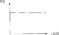
图3是表示依据LCD板电流消耗量的第一驱动电压理想水平的示意图。FIG. 3 is a schematic diagram showing an ideal level of a first driving voltage according to the current consumption of the LCD panel.
图4是表示依照本发明实施例的LCD驱动电压发生电路的方框图。FIG. 4 is a block diagram showing an LCD driving voltage generating circuit according to an embodiment of the present invention.
图5是依照本发明实施例的LCD驱动电压发生电路的详尽示意图;5 is a detailed schematic diagram of an LCD driving voltage generating circuit according to an embodiment of the present invention;
图6是表示图4所示DC-DC变换器的详细结构的电路图;Fig. 6 is a circuit diagram showing a detailed structure of the DC-DC converter shown in Fig. 4;
图7是表示图4所示压控振荡器的详细结构的电路图;Fig. 7 is a circuit diagram showing the detailed structure of the voltage controlled oscillator shown in Fig. 4;
图8是图5所示电压放大器的特性曲线图;Fig. 8 is a characteristic curve diagram of the voltage amplifier shown in Fig. 5;
图9是图4所示压控振荡器的特性曲线图;Fig. 9 is a characteristic curve diagram of the voltage-controlled oscillator shown in Fig. 4;
图10是图4所示驱动电压发生电路中增压效率相对时钟信号频率的特性曲线图。FIG. 10 is a characteristic curve of boosting efficiency versus clock signal frequency in the driving voltage generating circuit shown in FIG. 4 .
具体实施方式Detailed ways
现在将参照示出了本发明优选实施例的附图来更详细地描述本发明。不同附图中的相似参考数字指相似元件。The invention will now be described in more detail with reference to the accompanying drawings showing preferred embodiments of the invention. Like reference numbers in different drawings refer to like elements.
首先描述增压效率与用于增压的时钟信号的频率之间的关系。在此将时钟信号频率称为“增压频率”。First, the relationship between the supercharging efficiency and the frequency of the clock signal for supercharging will be described. The clock signal frequency is referred to herein as the "boost frequency".
图2是表示依据时钟信号频率FCK的增压效率与LCD板电流消耗ILOAD之间关系的曲线图。参照图2,如果LCD板ILOAD的电流消耗增加,不管时钟信号频率FCK的值如何,增压效率都会下降。但是,如果时钟信号的频率FCK为390KHz,那么由于电流消耗ILOAD的增加而对增压效率产生的影响将比时钟信号频率FCK为230KHz时的情况小得多。换句话说,如果时钟信号的频率为230KHz,那么第一驱动电压V0的电平将因电流消耗ILOAD的增加而下降很多。相反,如果时钟信号的频率为390KHz,第一驱动电压V0的电平将随电流消耗量的增加而下降较小的量。于是,在LCD板的电流消耗ILOAD很高时,通过提高增压频率FCK可以提高增压效率。FIG. 2 is a graph showing the relationship between boosting efficiency and LCD panel current consumption ILOAD according to the clock signal frequency FCK. Referring to FIG. 2, if the current consumption of the LCD panel ILOAD increases, the boosting efficiency will decrease regardless of the value of the clock signal frequency FCK. However, if the frequency FCK of the clock signal is 390KHz, the impact on boosting efficiency due to the increase of the current consumption ILOAD will be much smaller than when the frequency FCK of the clock signal is 230KHz. In other words, if the frequency of the clock signal is 230 KHz, then the level of the first driving voltage V0 will decrease a lot due to the increase of the current consumption ILOAD. On the contrary, if the frequency of the clock signal is 390 KHz, the level of the first driving voltage V0 will decrease by a small amount as the current consumption increases. Therefore, when the current consumption ILOAD of the LCD panel is high, the boosting efficiency can be improved by increasing the boosting frequency FCK.
另一方面,在LCD板的电流消耗ILOAD非常低时,提高增压频率FCK不会对增压效率产生很大影响。要注意的是,由图2实验结果所示的增压效率和功率消耗看出,根据LCD板的电流消耗ILOAD改变增压频率FCK是很有效的。On the other hand, when the current consumption ILOAD of the LCD panel is very low, increasing the boost frequency FCK will not have a great impact on the boost efficiency. It should be noted that it is effective to change the boosting frequency FCK according to the current consumption ILOAD of the LCD panel from the boosting efficiency and power consumption shown in the experimental results in Fig. 2 .
于是,当LCD板的负荷改变时,可根据LCD板的负荷(即电流消耗)而将增压频率变为最佳频率,以维持驱动电压的电平。优选的是,如图3所示,尽管电流消耗改变,增压效率也不降低,而第一驱动电压V0的电平仍维持在一定电平。Thus, when the load of the LCD panel changes, the boost frequency can be changed to an optimum frequency according to the load (ie, current consumption) of the LCD panel to maintain the level of the driving voltage. Preferably, as shown in FIG. 3 , the level of the first driving voltage V0 is maintained at a certain level even though the current consumption is changed without decreasing the boosting efficiency.
图4是依照本发明实施例的LCD驱动电压发生电路200的方框图。参照图4,依照本发明实施例的驱动电压发生电路200包括:DC-DC变换器210,驱动电压分压器220,反馈分压器230,参考电压发生器240,比较器250,控制电压发生器260以及压控振荡器270。FIG. 4 is a block diagram of an LCD driving
DC-DC变换器210接收输入电压VCI,对输入电压VCI进行增压,从而产生第一驱动电压V0。DC-DC变换器210仅在被起动信号EN起动时才响应时钟信号,通过注入电荷对输入电压VCI进行增压。DC-DC变换器210将输入电压VCI增大,使其成为比VCI大预定倍数的电压。(在此称之为“增压倍数”)The DC-
例如,如果将DC-DC变换器210配置成输入电压为3V,增压倍数为4,它能产生的最大第一驱动电压V0为12V。如果LCD板需要的第一驱动电压V0是9V,该电压低于第一驱动电压V0的最大电压12V,由于驱动LCD板所需的高电压仅为9V,因此就不必将驱动电压增到12V。于是,如果第一驱动电压V0达到目标值9V,为了避免不必要的功率消耗,期望的是停止第一驱动电压V0的增压。For example, if the DC-
如上所述,将DC-DC变换器210配置成:只在第一驱动电压V0低于目标值时,才响应起动信号EN的激励而工作,由此对输入电压VCI进行增压。As described above, the DC-
比较器250将反馈电压VFB与参考电压VREF进行比较,产生控制DC-DC变换器210进行增压的起动信号EN。即,如果反映第一驱动电压V0的反馈电压VFB小于参考电压VREF,比较器250就产生被激励的起动信号EN。然后将起动信号EN作为输入提供给DC-DC变换器210,并以此控制变换器210的工作。优选的是反馈电压分压器230通过驱动第一驱动电压V0产生反馈电压VFB。The
DC-DC变换器210进行增压所需的时钟信号CK是从压控振荡器270输出的。压控振荡器270产生一频率根据控制电压VCON的电平而变化的时钟信号CK。控制电压VCON的电平根据反映第一驱动电压V0的反馈电压VFB与参考电压之间的差值而变化。The clock signal CK necessary for the DC-
反馈分压器230对第一驱动电压V0进行分压,产生反馈电压VFB。即,反馈分压器230对第一驱动电压V0进行分压,产生反馈电压VFB,将它提供给比较器250和控制电压发生器260。The
参考电压发生器240产生输入比较器250和控制电压发生器260的参考电压VREF。优选的是将参考电压发生器240设计成对功率、电压、温度等的波动不敏感。The
驱动电压分压器220接收第一驱动电压V0,对它进行分压,输出第二到第五分压电压V1-V4。第一到第五分压电压V0-V4和接地电压VSS输入LCD板中,用以驱动LCD板。The driving
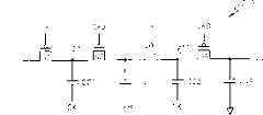
图5是依照本发明实施例的驱动电压发生电路200的详细示意方框图。图6是DC-DC变换器210的示意性方框图。参照图5,驱动电压分压器220包括第一到第五分压电阻R1-R5和第一到第四电压输出器221-224。第一到第五分压电阻R1-R5串联连接在第一驱动电压V0一接地电压VSS之间。第一分压电阻R1位于第一驱动电压V0与第一节点N1之间,第二分压电阻R2设置在第一节点N1与第二节点N2之间,第三分压电阻R3设置在第二节点N2与第三节点N3之间,第四分压电阻R4设置在第三节点N3与第四节点N4之间,第五分压电阻R5设置在第四节点N4与接地电压VSS之间。N1-N4中每个节点的电压都作为第二到第五驱动电压V1-V4通过电压输出器221-224输出。FIG. 5 is a detailed schematic block diagram of the driving
于是,第二到第五驱动电压V1-V4变为电平介于第一驱动电压V0和接地电压VSS之间的电压。反馈分压器230包括两个分压电阻Ra和Rb。由反馈分压器230产生的反馈电压VFB由分压电阻Ra与Rb的比值和第一驱动电压V0决定。优选的是,这样设置分压电阻Ra和Rb的值:如果第一驱动电压是预定目标值,反馈电压VFB与参考电压VRFE相同。Then, the second to fifth driving voltages V1-V4 become voltages having a level between the first driving voltage V0 and the ground voltage VSS. The
利用运算放大器配备参考电压发生器240,所述运算放大器能通过正(+)端子接收偏压VBIAS,通过负端子(-)接收反馈电压。第二反馈电压是通过利用两个电阻器R6和R7对参考电压VREF进行分压而产生的。The
比较器250通过正(+)端子接收反馈电压VFB,通过负(-)端子接收参考电压VREF。如果反馈电压VFB高于参考电压VREF,就输出高电平起动信号EN,如果反馈电压VFB低于参考电压VREF,就输出低电平起动信号EN。DC-DC变换器210响应低电平的起动信号EN对电压V0实施增压操作。The
于是,如果反馈电压VFB低于参考电压VREF,比较器250产生能起动DC-DC变换器210的起动信号EN。低于参考电压VREF的反馈电压VFB表示第一驱动电压V0低于理想目标值。因此,如果第一驱动电压V0低于目标值,就致使起动信号EN变到低电平。于是,第一驱动电压V0由于DC-DC变换器210进行的增压而增大。如果DC-DC变换器210的输出高于目标值,反馈电压VFB就会高于参考电压VREF。因此,就会禁止起动信号EN,从而使DC-DC变换器210的增压终止。Therefore, if the feedback voltage VFB is lower than the reference voltage VREF, the
控制电压发生器260包括电压放大器261、两个缓冲器262a和262b。缓冲器262a和262b分别对参考电压VREF和反馈电压VFB进行缓冲。电压放大器261产生与参考电压和反馈电压VFB的差值成比例的电压。于是,如果反馈电压VFB低于参考电压VREF,就会产生较高电平的控制电压VCON,而如果反馈电压VFB高于参考电压VREF,就产生较低电平的控制电压VCON。反馈电压VFB低于参考电压VREF表示第一驱动电压V0低于目标值。另外,如果第一驱动电压V0低于目标值,就表示LCD板中存在很大负载。The
可将电压放大器261配置成运算放大器,用以通过正(+)端子接收参考电压VREF,通过负(-)端子接收反馈电压VFB。由电压放大器261输出的控制电压VCON输入到压控振荡器270。压控振荡器270产生一频率根据输入的控制电压VCON的电平变化的时钟信号CK。即,如果控制电压VCON的电平较高,就会产生较高频率的时钟信号。如果控制电压VCON的电平较低,就产生频率较低的时钟信号。压控振荡器270的详细结构示于图7中。The
图6是DC-DC变换器210的实施例的详细示意图。但是,本发明的DC-DC变换器210并不限于图6的实施例,而是它可以采取多种适宜形式中的任何一种。DC-DC变换器210至少包括一个切换开关和电容器。在该实施例中,DC-DC变换器210包括四个切换开关和四个电容器。DC-DC变换器210中包含的四个切换开关被称为第一到第四切换开关S1-S4,而四个电容器被称为第一到第四电容器CC1-CC4。FIG. 6 is a detailed schematic diagram of an embodiment of the DC-
在一个实施例中,第一到第四切换开关S1-S4是MOS晶体管,用以通过栅极接收切换信号,在图6中,将第一到第四切换开关S1-S4配置成PMOS晶体管。第一到第四切换开关S1-S4串联接在输入电压VCI端子和输出电压端子(即,第一驱动电压V0)之间。另外,第一到第四切换开关S1-S4的输出端子与第一到第四电容器CC1-CC4相接。In one embodiment, the first to fourth switches S1-S4 are MOS transistors for receiving switching signals through gates. In FIG. 6, the first to fourth switches S1-S4 are configured as PMOS transistors. The first to fourth switching switches S1-S4 are connected in series between the input voltage VCI terminal and the output voltage terminal (ie, the first driving voltage V0). In addition, the output terminals of the first to fourth changeover switches S1-S4 are connected to the first to fourth capacitors CC1-CC4.
第一和第三切换开关S1和S3接收时钟信号CK作为切换信号,而第二和第四切换开关S2和S4接收反相时钟信号CKB作为切换信号。另外,第一和第三电容器CC1和CC3的对侧端子接收时钟信号CK,第二电容器CC2接收反相时钟信号CKB。优选的是,时钟信号CK是在接地电压VSS和输入电压VCI电平之间波动的信号。The first and third switching switches S1 and S3 receive the clock signal CK as a switching signal, and the second and fourth switching switches S2 and S4 receive an inverted clock signal CKB as a switching signal. In addition, opposite-side terminals of the first and third capacitors CC1 and CC3 receive the clock signal CK, and the second capacitor CC2 receives the inverted clock signal CKB. Preferably, the clock signal CK is a signal fluctuating between the ground voltage VSS and the input voltage VCI level.
通过这种方式,第一切换节点211的电压电平在输入电压VCI的电平和两倍输入电压电平2VCI之间波动,第二切换节点212处的电压电平在两倍输入电压电平2VCI和三倍输入电压电平3VCI之间波动,而第三切换节点213的电压电平在三倍输入电压3VCI和四倍输入电压4VCI之间波动。于是,第一驱动电压V0的电平几乎是输入电压VCI的三倍。即,将图6中的DC-DC变换器210设计成能将电压增大三倍。In this way, the voltage level of the
增压倍数可根据级数而改变。在此,级数由与时钟信号CK或反相时钟信号CKB相连的电容器的数目决定。图6中级数为3。The boost ratio can be changed according to the number of stages. Here, the number of stages is determined by the number of capacitors connected to the clock signal CK or the inverted clock signal CKB. The number of stages in Figure 6 is 3.
图7是图4所示压控振荡器实施例的示意图。存在多种不同方式体现压控振荡器。所示实施例包括环形振荡器,其中利用电阻值随施加电压变化的电阻器,可改变反相器链路输出节点中的有效电容值。FIG. 7 is a schematic diagram of an embodiment of the VCO shown in FIG. 4 . There are many different ways to implement a voltage controlled oscillator. The illustrated embodiment includes a ring oscillator in which the effective capacitance value in the output node of the inverter chain can be varied using a resistor whose resistance value varies with applied voltage.
参照图7,压控振荡器270包括:反相器链路,其包括多个串联连接的反相器271、272、和273;与每个反相器的输出节点相连的多个电阻器RM1、RM2和RM3;以及分别设置在电阻器RM1、RM2和RM3与接地电压之间的多个电容器CP1、CP2和CP3。Referring to FIG. 7, the voltage controlled
反相器链路的输出是具有增压频率FCK的时钟信号CK。反相器链路的输出反馈回到反相器链路的输入中。优选的是,电阻器RM1、RM2和RM3是能通过栅极接收控制电压VCON的NMOS晶体管。电阻RM1、RM2和RM3的漏极分别与反相器271、272和273的输出相连,电阻RM1、RM2和RM3的源极分别与电容器CP1、CP2和CP3相连。随着施加给栅极的控制电压VCON的电平增大,每个NMOS晶体管的电阻值会减小,随着施加给栅极的控制电压VCON的电平减小,它们的电阻值增大。反相器输出节点处的有效电容根据控制电压VCON的电平变化而变化。The output of the inverter chain is a clock signal CK with boost frequency FCK. The output of the inverter chain is fed back into the input of the inverter chain. Preferably, the resistors RM1, RM2 and RM3 are NMOS transistors capable of receiving the control voltage VCON through their gates. The drains of the resistors RM1, RM2 and RM3 are respectively connected to the outputs of the inverters 271, 272 and 273, and the sources of the resistors RM1, RM2 and RM3 are connected to the capacitors CP1, CP2 and CP3 respectively. As the level of the control voltage VCON applied to the gate increases, the resistance value of each NMOS transistor decreases, and as the level of the control voltage VCON applied to the gate decreases, their resistance values increase. The effective capacitance at the output node of the inverter changes according to the level change of the control voltage VCON.
如上所述,电阻RM1、RM2和RM3的电阻值根据施加的控制电压VCON而变化。随着有效电容变化,在反相器的输出信号与输入信号之间存在一定延迟值。因此,由反相器链路输出的时钟信号CK的频率也变化。As described above, the resistance values of the resistors RM1, RM2, and RM3 vary according to the applied control voltage VCON. As the effective capacitance changes, there is a certain delay value between the output signal of the inverter and the input signal. Consequently, the frequency of the clock signal CK output by the inverter chain also varies.
如果控制电压VCON很高,电阻器RM1、RM2和RM3的电阻就会降低。于是,延迟时间减少,时钟信号CK的频率增大。另一方面,如果控制电压VCON很低,电阻器RM1、RM2和RM3的电阻就会增大。于是,延迟时间增加,时钟信号CK的频率就会减小。If the control voltage VCON is high, the resistance of the resistors RM1, RM2 and RM3 will decrease. Thus, the delay time is reduced and the frequency of the clock signal CK is increased. On the other hand, if the control voltage VCON is low, the resistances of the resistors RM1, RM2 and RM3 will increase. Therefore, as the delay time increases, the frequency of the clock signal CK decreases.
图8是表示图5所示控制电压发生器260的电压放大器261的特性曲线图。电压放大器261产生控制电压VCON。控制电压VCON的电平与参考电压VREF与反馈电压VFB之间的差值电压VD成比例增大。其斜率被称为电压增益Av。FIG. 8 is a graph showing the characteristics of the
图9是表示图4所示压控振荡器270的特性的曲线图。参照图9,从压控振荡器270输出的时钟信号的频率FCK与输入的控制电压VCON成比例而变化。其斜率被称为电压-频率灵敏度Kv。FIG. 9 is a graph showing the characteristics of the voltage-controlled
要注意的是,时钟信号频率FCK的变化范围是由控制电压发生器260的电压放大器261的电压增益Av和压控振荡器270的电压-频率灵敏度Kv决定的。如果将增益频率的变化范围设置得很小,那么也就将控制电压发生器260的电压放大器的电压增益Av设置得很小。因此可将电压放大器261用作特定情况的衰减器。It should be noted that the variation range of the clock signal frequency FCK is determined by the voltage gain Av of the
图10是表示系统增压效率响应时钟信号频率FCK的曲线图。参照图10,随着时钟信号频率FCK增加,增压效率也增加到某一频率(图10中的F2)。如上所述,将通过第一驱动电压V0的目标值与实际第一驱动电压V0的比值求出的增压信号表示成百分比。FIG. 10 is a graph showing system supercharging efficiency in response to clock signal frequency FCK. Referring to FIG. 10, as the clock signal frequency FCK increases, the boosting efficiency also increases up to a certain frequency (F2 in FIG. 10). As described above, the boost signal obtained from the ratio of the target value of the first drive voltage V0 to the actual first drive voltage V0 is expressed as a percentage.
参照图10,如果时钟信号的频率FCK大于某一临界值,增压效率就不会再增加,随着增压频率FCK增大,其维持不变或降低。也就是说,如果时钟信号的频率FCK增加很大,DC-DC变换器210的增压效率就会降低。换句话说,随着增压频率增大,随DC-DC变换器210中消耗电流的增大变得更显著,效率降低。于是,如果增压频率FCK增大,使效率进一步增大是不可能的。Referring to FIG. 10 , if the frequency FCK of the clock signal is greater than a certain critical value, the supercharging efficiency will not increase any more, and it will remain unchanged or decrease as the supercharging frequency FCK increases. That is, if the frequency FCK of the clock signal increases greatly, the boosting efficiency of the DC-
因此,可将时钟信号的频率FCK控制在图10所示的线性范围F1-F2内。如上所述,可通过调节图8到图9中所示的电压增益Av和/或电压-频率灵敏度Kv,来控制时钟信号CK的频率范围。Therefore, the frequency FCK of the clock signal can be controlled within the linear range F1-F2 shown in FIG. 10 . As mentioned above, the frequency range of the clock signal CK can be controlled by adjusting the voltage gain Av and/or the voltage-frequency sensitivity Kv shown in FIGS. 8 to 9 .
要注意的是,本发明并不限于上述优选实施例,显而易见的是,在所附权利要求限定的本发明的精神和范围内,本领域的技术人员可以作出变化和改进。It should be noted that the present invention is not limited to the preferred embodiments described above, and it is obvious that changes and modifications can be made by those skilled in the art within the spirit and scope of the present invention as defined by the appended claims.
依照本发明,在LCD板的电流消耗很低时,例如在符号显示过程中,通过以非常低的增压频率驱动DC-DC变换器,可以降低DC-DC变换器消耗的消耗电流量。另一方面,在LCD的电流消耗很高时,例如在移动图象显示过程中,可通过增大增压频率来避免驱动电压的电平降低,从而增大增压效率。According to the present invention, the amount of current consumed by the DC-DC converter can be reduced by driving the DC-DC converter at a very low boost frequency when the current consumption of the LCD panel is low, such as during symbol display. On the other hand, when the current consumption of the LCD is high, such as during moving image display, the level reduction of the driving voltage can be avoided by increasing the boosting frequency, thereby increasing the boosting efficiency.
因此,即使LCD板的电流消耗增大,也可以维持显示质量,同时降低功率消耗,提高增压效率。Therefore, even if the current consumption of the LCD panel increases, display quality can be maintained while reducing power consumption and increasing boosting efficiency.
Claims (18)
Applications Claiming Priority (3)
| Application Number | Priority Date | Filing Date | Title |
|---|---|---|---|
| KR22323/02 | 2002-04-23 | ||
| KR22323/2002 | 2002-04-23 | ||
| KR10-2002-0022323AKR100438786B1 (en) | 2002-04-23 | 2002-04-23 | LCD driving voltage generation circuit having low power, high efficiency and Method there-of |
Publications (2)
| Publication Number | Publication Date |
|---|---|
| CN1453762Atrue CN1453762A (en) | 2003-11-05 |
| CN100390853C CN100390853C (en) | 2008-05-28 |
Family
ID=29267885
Family Applications (1)
| Application Number | Title | Priority Date | Filing Date |
|---|---|---|---|
| CNB031067123AExpired - Fee RelatedCN100390853C (en) | 2002-04-23 | 2003-02-27 | High-efficiency liquid crystal display driving voltage generating circuit and method thereof |
Country Status (5)
| Country | Link |
|---|---|
| US (2) | US7133038B2 (en) |
| JP (1) | JP4632113B2 (en) |
| KR (1) | KR100438786B1 (en) |
| CN (1) | CN100390853C (en) |
| TW (1) | TW589610B (en) |
Cited By (9)
| Publication number | Priority date | Publication date | Assignee | Title |
|---|---|---|---|---|
| CN100353651C (en)* | 2004-08-11 | 2007-12-05 | 统宝光电股份有限公司 | DC/DC converter and DC power supply system |
| CN100489931C (en)* | 2004-09-06 | 2009-05-20 | 索尼株式会社 | Image display unit and method of driving the same |
| CN102237059A (en)* | 2010-05-07 | 2011-11-09 | 硅工厂股份有限公司 | Boost converter for liquid crystal display |
| CN102270928A (en)* | 2010-06-07 | 2011-12-07 | 联咏科技股份有限公司 | Power conversion device and power conversion method |
| CN102543005A (en)* | 2010-12-21 | 2012-07-04 | 美格纳半导体有限公司 | Reference voltage generating circuit and LED driver circuit having the same therein |
| CN102684618A (en)* | 2011-02-25 | 2012-09-19 | 马克西姆综合产品公司 | Vcom switching amplifier |
| CN108227807A (en)* | 2017-12-29 | 2018-06-29 | 深圳市华星光电技术有限公司 | A kind of voltage control circuit, display and voltage control method |
| CN111477194A (en)* | 2020-05-27 | 2020-07-31 | 京东方科技集团股份有限公司 | Common voltage output circuit, display device and common voltage compensation method |
| WO2020200027A1 (en)* | 2019-04-04 | 2020-10-08 | 惠科股份有限公司 | Driving method for power supply drive circuit, power supply drive circuit and display device |
Families Citing this family (42)
| Publication number | Priority date | Publication date | Assignee | Title |
|---|---|---|---|---|
| KR100438786B1 (en)* | 2002-04-23 | 2004-07-05 | 삼성전자주식회사 | LCD driving voltage generation circuit having low power, high efficiency and Method there-of |
| KR100504475B1 (en)* | 2002-10-30 | 2005-08-03 | 엘지전자 주식회사 | Method for controlling function of organic electro-luminescence driving module |
| KR100928486B1 (en)* | 2002-12-31 | 2009-11-26 | 엘지디스플레이 주식회사 | Driving circuit of liquid crystal display device |
| KR100602065B1 (en)* | 2003-07-31 | 2006-07-14 | 엘지전자 주식회사 | Power supply device and its driving method and driving device and driving method of electroluminescence display device using the same |
| US7176877B2 (en)* | 2003-10-10 | 2007-02-13 | Nano-Proprietary, Inc. | High voltage pulse driver with capacitive coupling |
| GB2410826A (en)* | 2004-02-07 | 2005-08-10 | Sharp Kk | Active matrix liquid crystal display |
| US20050200621A1 (en)* | 2004-03-15 | 2005-09-15 | Arima Display Corporation | Power supply device of LCD module, LCD module of regulating working voltage and method of regulating power supply of LCD module |
| KR101056373B1 (en)* | 2004-09-07 | 2011-08-11 | 삼성전자주식회사 | Analog driving voltage and common electrode voltage generator of liquid crystal display and analog driving voltage and common electrode voltage control method of liquid crystal display |
| KR101178066B1 (en)* | 2005-10-11 | 2012-09-03 | 엘지디스플레이 주식회사 | Driving method for LCD |
| KR20070066633A (en)* | 2005-12-22 | 2007-06-27 | 삼성전자주식회사 | Drive device and display device including same |
| CN101000738A (en)* | 2006-01-11 | 2007-07-18 | 松下电器产业株式会社 | Voltage generating system |
| GB0622898D0 (en)* | 2006-11-16 | 2006-12-27 | Liquavista Bv | Driving of electrowetting displays |
| KR101375864B1 (en)* | 2006-12-11 | 2014-03-17 | 삼성디스플레이 주식회사 | Voltage boosting circuit, voltage boosting/dropping circuit and liquid crystal display |
| US20080143697A1 (en)* | 2006-12-13 | 2008-06-19 | Tomokazu Kojima | Drive voltage control device |
| KR100844874B1 (en)* | 2006-12-27 | 2008-07-09 | 삼성전자주식회사 | Voltage generator for generating a plurality of boosting voltages and a liquid crystal display comprising the same |
| KR100871829B1 (en)* | 2007-06-22 | 2008-12-03 | 삼성전자주식회사 | Common voltage generator and method thereof with small area and high efficiency |
| KR20090018343A (en)* | 2007-08-17 | 2009-02-20 | 삼성전자주식회사 | A timing controller, a display device having the same, and a driving method of the display device |
| KR101332798B1 (en)* | 2007-08-29 | 2013-11-26 | 삼성디스플레이 주식회사 | Power generating module and liquid crystal dispaly having the smae |
| JP5178232B2 (en) | 2008-02-20 | 2013-04-10 | ルネサスエレクトロニクス株式会社 | Power circuit |
| CN101546216A (en)* | 2008-03-28 | 2009-09-30 | 鸿富锦精密工业(深圳)有限公司 | Reset circuit |
| JP5072731B2 (en)* | 2008-06-23 | 2012-11-14 | 株式会社東芝 | Constant voltage boost power supply |
| JP5242320B2 (en)* | 2008-09-29 | 2013-07-24 | 富士通テン株式会社 | Oscillation circuit and video display device |
| CN102460192B (en)* | 2009-06-26 | 2014-11-12 | 松下电器产业株式会社 | Electronic part and method of detecting faults therein |
| US8410371B2 (en)* | 2009-09-08 | 2013-04-02 | Cree, Inc. | Electronic device submounts with thermally conductive vias and light emitting devices including the same |
| US8067978B2 (en)* | 2009-10-13 | 2011-11-29 | Nanya Technology Corp. | Dynamic current supplying pump |
| KR101127580B1 (en)* | 2009-12-10 | 2012-03-26 | 삼성모바일디스플레이주식회사 | Power driver, source driver, and display apparatus |
| KR101128690B1 (en)* | 2009-12-17 | 2012-03-23 | 매그나칩 반도체 유한회사 | Circuit for generating boosted voltage and operatrion method of the same |
| US8461810B2 (en) | 2009-12-17 | 2013-06-11 | Magnachip Semiconductor, Ltd. | Circuit for generating boosted voltage and method for operating the same |
| TW201143289A (en)* | 2010-05-27 | 2011-12-01 | Novatek Microelectronics Corp | Power converting apparatus and power converting method |
| TWI441130B (en)* | 2011-10-18 | 2014-06-11 | Au Optronics Corp | Intergrated source driving system and displayer comprising the same |
| KR20130081451A (en)* | 2012-01-09 | 2013-07-17 | 삼성디스플레이 주식회사 | Display device and driving method thereof |
| US9761195B2 (en) | 2012-04-11 | 2017-09-12 | Sitronix Technology Corp. | Driving circuit for increasing a driving power supply voltage for a display panel |
| JP5894565B2 (en) | 2013-08-13 | 2016-03-30 | 株式会社東芝 | Regulator and switch device |
| CN103856044B (en)* | 2014-03-18 | 2016-07-06 | 中国科学院上海微系统与信息技术研究所 | A kind of charge pump circuit and output voltage Automatic adjustment method thereof |
| US9444614B2 (en)* | 2014-03-27 | 2016-09-13 | Synaptics Display Devices Gk | Dynamic power control for CDR |
| KR20160087466A (en)* | 2015-01-13 | 2016-07-22 | 삼성디스플레이 주식회사 | Display device |
| KR20160120055A (en) | 2015-04-07 | 2016-10-17 | 삼성전자주식회사 | Display device and operating method for the same |
| KR102417204B1 (en)* | 2017-10-11 | 2022-07-06 | 삼성디스플레이 주식회사 | Display device and driving method thereof |
| US10734083B2 (en)* | 2017-10-13 | 2020-08-04 | Ememory Technology Inc. | Voltage driver for memory |
| CN108922487B (en)* | 2018-08-24 | 2020-06-26 | 惠科股份有限公司 | Voltage regulating circuit and display device |
| KR102742420B1 (en)* | 2019-12-31 | 2024-12-13 | 엘지디스플레이 주식회사 | Display device and manufacturing method thereof |
| CN112165250B (en)* | 2020-10-12 | 2022-04-05 | 唯捷创芯(天津)电子技术股份有限公司 | Charge pump circuit, chip and communication terminal |
Family Cites Families (29)
| Publication number | Priority date | Publication date | Assignee | Title |
|---|---|---|---|---|
| US4859911A (en)* | 1987-02-13 | 1989-08-22 | International Business Machines Corporation | Power supply for electroluminescent panel |
| JPS63224664A (en)* | 1987-03-12 | 1988-09-19 | Seiko Instr & Electronics Ltd | Booster circuit |
| JP2952890B2 (en)* | 1989-06-22 | 1999-09-27 | 日本電気株式会社 | Display device |
| JP3050714B2 (en)* | 1993-02-26 | 2000-06-12 | 太陽誘電株式会社 | Voltage resonance type power supply circuit |
| JP3324819B2 (en)* | 1993-03-03 | 2002-09-17 | 三菱電機株式会社 | Semiconductor integrated circuit device |
| JP3159586B2 (en)* | 1993-12-09 | 2001-04-23 | 株式会社東芝 | Boost circuit device |
| JPH07202646A (en)* | 1993-12-28 | 1995-08-04 | Fujitsu Ltd | Voltage controlled oscillator |
| JPH0923639A (en)* | 1995-07-07 | 1997-01-21 | Seiko Epson Corp | Voltage converter |
| JPH0965651A (en)* | 1995-08-23 | 1997-03-07 | Minebea Co Ltd | Dc-dc converter device |
| JP3519870B2 (en)* | 1996-05-30 | 2004-04-19 | 三洋電機株式会社 | Liquid crystal display |
| JPH11136601A (en)* | 1997-10-27 | 1999-05-21 | Nec Kansai Ltd | Display converter for liquid crystal display panel and liquid crystal display device using the same |
| JPH11231840A (en)* | 1998-02-12 | 1999-08-27 | Sony Corp | Liquid crystal display device |
| JPH11252903A (en)* | 1998-03-03 | 1999-09-17 | Seiko Instruments Inc | Power circuit |
| JP3775628B2 (en)* | 1998-03-19 | 2006-05-17 | パイオニア株式会社 | Driving device and driving method of charge storage light emitting element |
| JP2000020147A (en)* | 1998-06-26 | 2000-01-21 | Casio Comput Co Ltd | Power source device |
| JP2000098346A (en)* | 1998-09-24 | 2000-04-07 | Mitsubishi Electric Corp | LCD drive voltage control circuit |
| ATE374384T1 (en)* | 1999-01-08 | 2007-10-15 | Seiko Epson Corp | LCD DEVICE, ELECTRONIC DEVICE AND POWER SUPPLY FOR DRIVING THE LCD |
| JP3025491B1 (en) | 1999-01-11 | 2000-03-27 | 日本ベアリング株式会社 | Bearing member |
| JP2000236657A (en)* | 1999-02-15 | 2000-08-29 | Nec Kyushu Ltd | Booster circuit |
| JP2000270540A (en)* | 1999-03-15 | 2000-09-29 | Texas Instr Japan Ltd | Voltage supply circuit |
| JP2000278937A (en)* | 1999-03-23 | 2000-10-06 | Hitachi Ltd | Booster circuit and power supply circuit for liquid crystal display device using the same |
| JP2000341939A (en)* | 1999-05-24 | 2000-12-08 | Nec Corp | Piezo transformer converter |
| JP2001282189A (en)* | 2000-03-29 | 2001-10-12 | Hitachi Ltd | Liquid crystal display |
| JP2001337651A (en)* | 2000-05-24 | 2001-12-07 | Nec Microsystems Ltd | Power supply circuit for driving liquid crystal display |
| KR100348275B1 (en)* | 2000-07-28 | 2002-08-09 | 엘지전자 주식회사 | driving control circuit in organic electroluminescence |
| JP4212791B2 (en)* | 2000-08-09 | 2009-01-21 | シャープ株式会社 | Liquid crystal display device and portable electronic device |
| JP2002238243A (en)* | 2001-02-07 | 2002-08-23 | Seiko Epson Corp | DC / DC converter and power supply for liquid crystal |
| JP2003295830A (en)* | 2002-03-29 | 2003-10-15 | Hitachi Ltd | Liquid crystal drive and liquid crystal display system |
| KR100438786B1 (en)* | 2002-04-23 | 2004-07-05 | 삼성전자주식회사 | LCD driving voltage generation circuit having low power, high efficiency and Method there-of |
- 2002
- 2002-04-23KRKR10-2002-0022323Apatent/KR100438786B1/ennot_activeExpired - Fee Related
- 2003
- 2003-02-07TWTW092102503Apatent/TW589610B/ennot_activeIP Right Cessation
- 2003-02-27CNCNB031067123Apatent/CN100390853C/ennot_activeExpired - Fee Related
- 2003-03-14JPJP2003070108Apatent/JP4632113B2/ennot_activeExpired - Fee Related
- 2003-04-17USUS10/417,585patent/US7133038B2/ennot_activeExpired - Fee Related
- 2006
- 2006-09-29USUS11/540,292patent/US7683898B2/ennot_activeExpired - Fee Related
Cited By (14)
| Publication number | Priority date | Publication date | Assignee | Title |
|---|---|---|---|---|
| CN100353651C (en)* | 2004-08-11 | 2007-12-05 | 统宝光电股份有限公司 | DC/DC converter and DC power supply system |
| CN100489931C (en)* | 2004-09-06 | 2009-05-20 | 索尼株式会社 | Image display unit and method of driving the same |
| CN102237059B (en)* | 2010-05-07 | 2013-11-06 | 硅工厂股份有限公司 | Boost converter for liquid crystal display |
| CN102237059A (en)* | 2010-05-07 | 2011-11-09 | 硅工厂股份有限公司 | Boost converter for liquid crystal display |
| US8633923B2 (en) | 2010-05-07 | 2014-01-21 | Silicon Works Co., Ltd. | Boost converter using frequency-varying oscillation signal for liquid crystal display |
| CN102270928A (en)* | 2010-06-07 | 2011-12-07 | 联咏科技股份有限公司 | Power conversion device and power conversion method |
| CN102543005A (en)* | 2010-12-21 | 2012-07-04 | 美格纳半导体有限公司 | Reference voltage generating circuit and LED driver circuit having the same therein |
| CN102543005B (en)* | 2010-12-21 | 2016-02-10 | 美格纳半导体有限公司 | Reference voltage generating circuit and utilize the LED drive circuit of this circuit |
| CN102684618A (en)* | 2011-02-25 | 2012-09-19 | 马克西姆综合产品公司 | Vcom switching amplifier |
| CN102684618B (en)* | 2011-02-25 | 2017-06-09 | 马克西姆综合产品公司 | VCOM switching amplifiers |
| CN108227807A (en)* | 2017-12-29 | 2018-06-29 | 深圳市华星光电技术有限公司 | A kind of voltage control circuit, display and voltage control method |
| WO2019127687A1 (en)* | 2017-12-29 | 2019-07-04 | 深圳市华星光电技术有限公司 | Voltage control circuit, display device, and voltage control method |
| WO2020200027A1 (en)* | 2019-04-04 | 2020-10-08 | 惠科股份有限公司 | Driving method for power supply drive circuit, power supply drive circuit and display device |
| CN111477194A (en)* | 2020-05-27 | 2020-07-31 | 京东方科技集团股份有限公司 | Common voltage output circuit, display device and common voltage compensation method |
Also Published As
| Publication number | Publication date |
|---|---|
| TW200305841A (en) | 2003-11-01 |
| TW589610B (en) | 2004-06-01 |
| US7683898B2 (en) | 2010-03-23 |
| US20070024555A1 (en) | 2007-02-01 |
| JP4632113B2 (en) | 2011-02-16 |
| KR100438786B1 (en) | 2004-07-05 |
| KR20030083922A (en) | 2003-11-01 |
| JP2004004609A (en) | 2004-01-08 |
| CN100390853C (en) | 2008-05-28 |
| US20050156854A1 (en) | 2005-07-21 |
| US7133038B2 (en) | 2006-11-07 |
Similar Documents
| Publication | Publication Date | Title |
|---|---|---|
| CN1453762A (en) | Efficient liquid crystal display drive voltage generating circuit and its method | |
| US9013229B2 (en) | Charge pump circuit | |
| CN101383558B (en) | Step-up power supply circuit and stepping-up method | |
| JP3700173B2 (en) | Voltage conversion control circuit and method | |
| CN1064470C (en) | Power circuit used for liquid crystal stimulation | |
| JP4895694B2 (en) | Power circuit | |
| CN103475213B (en) | Power supply circuit with multi-stage charge pump | |
| KR0151839B1 (en) | Power source circuit | |
| JP2006006004A (en) | Buck-boost DC-DC converter | |
| US20070063762A1 (en) | Semiconductor device with charge pump booster circuit | |
| CN1280413A (en) | boost circuit | |
| CN1674155A (en) | Power supply circuit and semiconductor storage device with the power supply circuit | |
| CN100520896C (en) | Low Power Multi-stage Driving Method for Liquid Crystal Display | |
| CN1703779A (en) | semiconductor integrated circuit | |
| CN1681191B (en) | Boost circuit and semiconductor integrated circuit | |
| TW200823842A (en) | Regulating circuit for common electrode voltage, driving circuit of liquid crystal panel and liquid crystal display using same | |
| CN1908740A (en) | Converter controller having feedforward compensation, converting system and method for controlling same | |
| CN113824315B (en) | Power generation circuit and display device | |
| CN1655431A (en) | Slow start charge pump circuit | |
| US7545170B2 (en) | Source driver and level shifting method thereof | |
| CN113630114B (en) | Driving circuit and electronic equipment | |
| CN115411932A (en) | A Charge Pump Circuit Structure for AMOLED Low Power Consumption, Low Starting Current and High Accuracy PWM Modulation | |
| CN2828860Y (en) | Switch controller with feedback compensation and conversion system | |
| CN115313853A (en) | AMOLED low-power-consumption low-starting-current PWM modulated charge pump circuit structure | |
| US8525818B2 (en) | Display system |
Legal Events
| Date | Code | Title | Description |
|---|---|---|---|
| C06 | Publication | ||
| PB01 | Publication | ||
| C10 | Entry into substantive examination | ||
| SE01 | Entry into force of request for substantive examination | ||
| C14 | Grant of patent or utility model | ||
| GR01 | Patent grant | ||
| C17 | Cessation of patent right | ||
| CF01 | Termination of patent right due to non-payment of annual fee | Granted publication date:20080528 Termination date:20140227 |