CN1449585A - Semiconductor device and manufacturing method thereof - Google Patents
Semiconductor device and manufacturing method thereofDownload PDFInfo
- Publication number
- CN1449585A CN1449585ACN01814948ACN01814948ACN1449585ACN 1449585 ACN1449585 ACN 1449585ACN 01814948 ACN01814948 ACN 01814948ACN 01814948 ACN01814948 ACN 01814948ACN 1449585 ACN1449585 ACN 1449585A
- Authority
- CN
- China
- Prior art keywords
- channel
- effect transistor
- field effect
- type field
- conductivity type
- Prior art date
- Legal status (The legal status is an assumption and is not a legal conclusion. Google has not performed a legal analysis and makes no representation as to the accuracy of the status listed.)
- Pending
Links
Images


Classifications
- H—ELECTRICITY
- H10—SEMICONDUCTOR DEVICES; ELECTRIC SOLID-STATE DEVICES NOT OTHERWISE PROVIDED FOR
- H10D—INORGANIC ELECTRIC SEMICONDUCTOR DEVICES
- H10D84/00—Integrated devices formed in or on semiconductor substrates that comprise only semiconducting layers, e.g. on Si wafers or on GaAs-on-Si wafers
- H10D84/01—Manufacture or treatment
- H10D84/0123—Integrating together multiple components covered by H10D12/00 or H10D30/00, e.g. integrating multiple IGBTs
- H10D84/0126—Integrating together multiple components covered by H10D12/00 or H10D30/00, e.g. integrating multiple IGBTs the components including insulated gates, e.g. IGFETs
- H10D84/0165—Integrating together multiple components covered by H10D12/00 or H10D30/00, e.g. integrating multiple IGBTs the components including insulated gates, e.g. IGFETs the components including complementary IGFETs, e.g. CMOS devices
- H10D84/0167—Manufacturing their channels
- H—ELECTRICITY
- H10—SEMICONDUCTOR DEVICES; ELECTRIC SOLID-STATE DEVICES NOT OTHERWISE PROVIDED FOR
- H10D—INORGANIC ELECTRIC SEMICONDUCTOR DEVICES
- H10D30/00—Field-effect transistors [FET]
- H10D30/60—Insulated-gate field-effect transistors [IGFET]
- H10D30/791—Arrangements for exerting mechanical stress on the crystal lattice of the channel regions
- H10D30/794—Arrangements for exerting mechanical stress on the crystal lattice of the channel regions comprising conductive materials, e.g. silicided source, drain or gate electrodes
- H—ELECTRICITY
- H01—ELECTRIC ELEMENTS
- H01L—SEMICONDUCTOR DEVICES NOT COVERED BY CLASS H10
- H01L21/00—Processes or apparatus adapted for the manufacture or treatment of semiconductor or solid state devices or of parts thereof
- H01L21/02—Manufacture or treatment of semiconductor devices or of parts thereof
- H01L21/02104—Forming layers
- H01L21/02107—Forming insulating materials on a substrate
- H01L21/02109—Forming insulating materials on a substrate characterised by the type of layer, e.g. type of material, porous/non-porous, pre-cursors, mixtures or laminates
- H01L21/02112—Forming insulating materials on a substrate characterised by the type of layer, e.g. type of material, porous/non-porous, pre-cursors, mixtures or laminates characterised by the material of the layer
- H01L21/02123—Forming insulating materials on a substrate characterised by the type of layer, e.g. type of material, porous/non-porous, pre-cursors, mixtures or laminates characterised by the material of the layer the material containing silicon
- H01L21/0217—Forming insulating materials on a substrate characterised by the type of layer, e.g. type of material, porous/non-porous, pre-cursors, mixtures or laminates characterised by the material of the layer the material containing silicon the material being a silicon nitride not containing oxygen, e.g. SixNy or SixByNz
- H—ELECTRICITY
- H01—ELECTRIC ELEMENTS
- H01L—SEMICONDUCTOR DEVICES NOT COVERED BY CLASS H10
- H01L21/00—Processes or apparatus adapted for the manufacture or treatment of semiconductor or solid state devices or of parts thereof
- H01L21/02—Manufacture or treatment of semiconductor devices or of parts thereof
- H01L21/04—Manufacture or treatment of semiconductor devices or of parts thereof the devices having potential barriers, e.g. a PN junction, depletion layer or carrier concentration layer
- H01L21/18—Manufacture or treatment of semiconductor devices or of parts thereof the devices having potential barriers, e.g. a PN junction, depletion layer or carrier concentration layer the devices having semiconductor bodies comprising elements of Group IV of the Periodic Table or AIIIBV compounds with or without impurities, e.g. doping materials
- H01L21/26—Bombardment with radiation
- H01L21/263—Bombardment with radiation with high-energy radiation
- H01L21/265—Bombardment with radiation with high-energy radiation producing ion implantation
- H01L21/26586—Bombardment with radiation with high-energy radiation producing ion implantation characterised by the angle between the ion beam and the crystal planes or the main crystal surface
- H—ELECTRICITY
- H10—SEMICONDUCTOR DEVICES; ELECTRIC SOLID-STATE DEVICES NOT OTHERWISE PROVIDED FOR
- H10D—INORGANIC ELECTRIC SEMICONDUCTOR DEVICES
- H10D30/00—Field-effect transistors [FET]
- H10D30/01—Manufacture or treatment
- H10D30/021—Manufacture or treatment of FETs having insulated gates [IGFET]
- H10D30/0212—Manufacture or treatment of FETs having insulated gates [IGFET] using self-aligned silicidation
- H—ELECTRICITY
- H10—SEMICONDUCTOR DEVICES; ELECTRIC SOLID-STATE DEVICES NOT OTHERWISE PROVIDED FOR
- H10D—INORGANIC ELECTRIC SEMICONDUCTOR DEVICES
- H10D30/00—Field-effect transistors [FET]
- H10D30/01—Manufacture or treatment
- H10D30/021—Manufacture or treatment of FETs having insulated gates [IGFET]
- H10D30/0223—Manufacture or treatment of FETs having insulated gates [IGFET] having source and drain regions or source and drain extensions self-aligned to sides of the gate
- H10D30/0227—Manufacture or treatment of FETs having insulated gates [IGFET] having source and drain regions or source and drain extensions self-aligned to sides of the gate having both lightly-doped source and drain extensions and source and drain regions self-aligned to the sides of the gate, e.g. lightly-doped drain [LDD] MOSFET or double-diffused drain [DDD] MOSFET
- H—ELECTRICITY
- H10—SEMICONDUCTOR DEVICES; ELECTRIC SOLID-STATE DEVICES NOT OTHERWISE PROVIDED FOR
- H10D—INORGANIC ELECTRIC SEMICONDUCTOR DEVICES
- H10D30/00—Field-effect transistors [FET]
- H10D30/60—Insulated-gate field-effect transistors [IGFET]
- H10D30/791—Arrangements for exerting mechanical stress on the crystal lattice of the channel regions
- H10D30/792—Arrangements for exerting mechanical stress on the crystal lattice of the channel regions comprising applied insulating layers, e.g. stress liners
- H—ELECTRICITY
- H10—SEMICONDUCTOR DEVICES; ELECTRIC SOLID-STATE DEVICES NOT OTHERWISE PROVIDED FOR
- H10D—INORGANIC ELECTRIC SEMICONDUCTOR DEVICES
- H10D84/00—Integrated devices formed in or on semiconductor substrates that comprise only semiconducting layers, e.g. on Si wafers or on GaAs-on-Si wafers
- H10D84/01—Manufacture or treatment
- H10D84/0123—Integrating together multiple components covered by H10D12/00 or H10D30/00, e.g. integrating multiple IGBTs
- H10D84/0126—Integrating together multiple components covered by H10D12/00 or H10D30/00, e.g. integrating multiple IGBTs the components including insulated gates, e.g. IGFETs
- H10D84/0165—Integrating together multiple components covered by H10D12/00 or H10D30/00, e.g. integrating multiple IGBTs the components including insulated gates, e.g. IGFETs the components including complementary IGFETs, e.g. CMOS devices
- H10D84/017—Manufacturing their source or drain regions, e.g. silicided source or drain regions
- H—ELECTRICITY
- H10—SEMICONDUCTOR DEVICES; ELECTRIC SOLID-STATE DEVICES NOT OTHERWISE PROVIDED FOR
- H10D—INORGANIC ELECTRIC SEMICONDUCTOR DEVICES
- H10D84/00—Integrated devices formed in or on semiconductor substrates that comprise only semiconducting layers, e.g. on Si wafers or on GaAs-on-Si wafers
- H10D84/01—Manufacture or treatment
- H10D84/0123—Integrating together multiple components covered by H10D12/00 or H10D30/00, e.g. integrating multiple IGBTs
- H10D84/0126—Integrating together multiple components covered by H10D12/00 or H10D30/00, e.g. integrating multiple IGBTs the components including insulated gates, e.g. IGFETs
- H10D84/0165—Integrating together multiple components covered by H10D12/00 or H10D30/00, e.g. integrating multiple IGBTs the components including insulated gates, e.g. IGFETs the components including complementary IGFETs, e.g. CMOS devices
- H10D84/0172—Manufacturing their gate conductors
- H10D84/0177—Manufacturing their gate conductors the gate conductors having different materials or different implants
- H—ELECTRICITY
- H10—SEMICONDUCTOR DEVICES; ELECTRIC SOLID-STATE DEVICES NOT OTHERWISE PROVIDED FOR
- H10D—INORGANIC ELECTRIC SEMICONDUCTOR DEVICES
- H10D84/00—Integrated devices formed in or on semiconductor substrates that comprise only semiconducting layers, e.g. on Si wafers or on GaAs-on-Si wafers
- H10D84/01—Manufacture or treatment
- H10D84/0123—Integrating together multiple components covered by H10D12/00 or H10D30/00, e.g. integrating multiple IGBTs
- H10D84/0126—Integrating together multiple components covered by H10D12/00 or H10D30/00, e.g. integrating multiple IGBTs the components including insulated gates, e.g. IGFETs
- H10D84/0165—Integrating together multiple components covered by H10D12/00 or H10D30/00, e.g. integrating multiple IGBTs the components including insulated gates, e.g. IGFETs the components including complementary IGFETs, e.g. CMOS devices
- H10D84/0184—Manufacturing their gate sidewall spacers
- H—ELECTRICITY
- H10—SEMICONDUCTOR DEVICES; ELECTRIC SOLID-STATE DEVICES NOT OTHERWISE PROVIDED FOR
- H10D—INORGANIC ELECTRIC SEMICONDUCTOR DEVICES
- H10D84/00—Integrated devices formed in or on semiconductor substrates that comprise only semiconducting layers, e.g. on Si wafers or on GaAs-on-Si wafers
- H10D84/01—Manufacture or treatment
- H10D84/02—Manufacture or treatment characterised by using material-based technologies
- H10D84/03—Manufacture or treatment characterised by using material-based technologies using Group IV technology, e.g. silicon technology or silicon-carbide [SiC] technology
- H10D84/038—Manufacture or treatment characterised by using material-based technologies using Group IV technology, e.g. silicon technology or silicon-carbide [SiC] technology using silicon technology, e.g. SiGe
- H—ELECTRICITY
- H10—SEMICONDUCTOR DEVICES; ELECTRIC SOLID-STATE DEVICES NOT OTHERWISE PROVIDED FOR
- H10D—INORGANIC ELECTRIC SEMICONDUCTOR DEVICES
- H10D84/00—Integrated devices formed in or on semiconductor substrates that comprise only semiconducting layers, e.g. on Si wafers or on GaAs-on-Si wafers
- H10D84/80—Integrated devices formed in or on semiconductor substrates that comprise only semiconducting layers, e.g. on Si wafers or on GaAs-on-Si wafers characterised by the integration of at least one component covered by groups H10D12/00 or H10D30/00, e.g. integration of IGFETs
- H10D84/82—Integrated devices formed in or on semiconductor substrates that comprise only semiconducting layers, e.g. on Si wafers or on GaAs-on-Si wafers characterised by the integration of at least one component covered by groups H10D12/00 or H10D30/00, e.g. integration of IGFETs of only field-effect components
- H10D84/83—Integrated devices formed in or on semiconductor substrates that comprise only semiconducting layers, e.g. on Si wafers or on GaAs-on-Si wafers characterised by the integration of at least one component covered by groups H10D12/00 or H10D30/00, e.g. integration of IGFETs of only field-effect components of only insulated-gate FETs [IGFET]
- H10D84/85—Complementary IGFETs, e.g. CMOS
- H10D84/856—Complementary IGFETs, e.g. CMOS the complementary IGFETs having different architectures than each other, e.g. high-voltage and low-voltage CMOS
- H—ELECTRICITY
- H10—SEMICONDUCTOR DEVICES; ELECTRIC SOLID-STATE DEVICES NOT OTHERWISE PROVIDED FOR
- H10D—INORGANIC ELECTRIC SEMICONDUCTOR DEVICES
- H10D86/00—Integrated devices formed in or on insulating or conducting substrates, e.g. formed in silicon-on-insulator [SOI] substrates or on stainless steel or glass substrates
- H10D86/01—Manufacture or treatment
- H—ELECTRICITY
- H01—ELECTRIC ELEMENTS
- H01L—SEMICONDUCTOR DEVICES NOT COVERED BY CLASS H10
- H01L2924/00—Indexing scheme for arrangements or methods for connecting or disconnecting semiconductor or solid-state bodies as covered by H01L24/00
- H01L2924/0001—Technical content checked by a classifier
- H01L2924/0002—Not covered by any one of groups H01L24/00, H01L24/00 and H01L2224/00
Landscapes
- Engineering & Computer Science (AREA)
- Physics & Mathematics (AREA)
- Condensed Matter Physics & Semiconductors (AREA)
- General Physics & Mathematics (AREA)
- Manufacturing & Machinery (AREA)
- Computer Hardware Design (AREA)
- Microelectronics & Electronic Packaging (AREA)
- Power Engineering (AREA)
- High Energy & Nuclear Physics (AREA)
- Chemical & Material Sciences (AREA)
- Crystallography & Structural Chemistry (AREA)
- Health & Medical Sciences (AREA)
- Toxicology (AREA)
- Metal-Oxide And Bipolar Metal-Oxide Semiconductor Integrated Circuits (AREA)
- Insulated Gate Type Field-Effect Transistor (AREA)
- Thin Film Transistor (AREA)
- Electrodes Of Semiconductors (AREA)
- Internal Circuitry In Semiconductor Integrated Circuit Devices (AREA)
- Materials Engineering (AREA)
- Semiconductor Memories (AREA)
- Formation Of Insulating Films (AREA)
- Chemical Kinetics & Catalysis (AREA)
Abstract
Description
Translated fromChinese技术领域technical field
本发明涉及半导体器件及其制造技术,特别涉及应用于在同一基板上具有n沟道导电型MISFET及p沟道导电型MISFET的半导体器件及其制造技术的有效技术。The present invention relates to a semiconductor device and its manufacturing technology, in particular to an effective technology applied to a semiconductor device having an n-channel conductivity type MISFET and a p-channel conductivity type MISFET on the same substrate and its manufacturing technology.
背景技术Background technique
作为搭载在半导体器件上的场效应晶体管,被称为MISFET(Metal Insulator Semiconductor Field Effect Transistor:金属绝缘物半导体场效应晶体管)的绝缘栅型场效应晶体管是公知的。该MISFET具有易于高集成化的特征,所以作为构成集成电路的电路元件正被广泛使用。An insulated gate field effect transistor called MISFET (Metal Insulator Semiconductor Field Effect Transistor) is known as a field effect transistor mounted on a semiconductor device. Since the MISFET is characterized by being easy to be highly integrated, it is widely used as a circuit element constituting an integrated circuit.
无论n沟道导电型还是p沟道导电型,MISFET一般被构成为具由沟道形成区域、栅极绝缘膜、栅极电极、源区和漏区等。栅极绝缘膜设在半导体基板的电路形成面(一主面)的元器件形成区域,例如形成在氧化硅膜上。栅极电极设在半导体基板的电路形成面的元件形成区域上的栅极绝缘膜上,例如形成在掺入了使电阻值降低的杂质的多晶硅膜上。沟道形成区域设在与栅极电极对置的半导体基板的区域(在栅极电极正下方)。源区和漏区形成于设在沟道形成区域的沟道长度方向两侧的半导体区域(杂质扩散区域)。Regardless of the n-channel conductivity type or the p-channel conductivity type, a MISFET is generally configured to have a channel formation region, a gate insulating film, a gate electrode, a source region, a drain region, and the like. The gate insulating film is provided in a component formation region of the circuit formation surface (one main surface) of the semiconductor substrate, and is formed, for example, on a silicon oxide film. The gate electrode is provided on a gate insulating film in an element formation region on a circuit formation surface of a semiconductor substrate, for example, a polysilicon film doped with an impurity that lowers a resistance value. The channel formation region is provided in a region of the semiconductor substrate facing the gate electrode (immediately below the gate electrode). The source region and the drain region are formed in semiconductor regions (impurity diffusion regions) provided on both sides in the channel length direction of the channel formation region.
并且,在MISFET中,栅极绝缘膜是由氧化硅膜形成的通常被称为MOSFET(Metal Oxide Semiconductor Field Effect Transistor:金属氧化物半导体场效应晶体管)。而且,所谓沟道形成区域是指连接源区和漏区的电流通道(沟道)的区域而言。Also, in MISFET, the gate insulating film is formed of a silicon oxide film, which is generally called MOSFET (Metal Oxide Semiconductor Field Effect Transistor: Metal Oxide Semiconductor Field Effect Transistor). In addition, the term "channel formation region" refers to a region of a current passage (channel) connecting a source region and a drain region.
发明的公开disclosure of invention
但是,在0.1μm级时代的超微细CMIS(Complementary MIS)工艺中,由于新材料的导入、MISFET短沟道效应的抑制等原因,使低温化正在进展中。这使得在元件中易于残留因工艺引起的残留应力。工艺引起的残留应力作用于半导体基板的电路形成面的表面,即MISFET的沟道形成区域。However, in the ultra-fine CMIS (Complementary MIS) process of the 0.1 μm class era, due to the introduction of new materials and the suppression of the short-channel effect of MISFETs, the lowering of the temperature is progressing. This makes it easy for process-induced residual stress to remain in the component. The residual stress caused by the process acts on the surface of the circuit formation surface of the semiconductor substrate, that is, the channel formation region of the MISFET.
在一般的CMIS(互补型MIS)工艺中,例如在半导体基板的电路形成面上形成层间绝缘膜的情况下,在n沟道导电型MISFET及p沟道导电型MISFET使用相同材料而引起的结果是:作用于同一芯片内的MISFET的沟道形成区域的应力大致相等。另外,通常通过改良工艺,实现减小作用于MISFET的沟道形成区域的应力。In a general CMIS (complementary MIS) process, for example, when an interlayer insulating film is formed on the circuit formation surface of a semiconductor substrate, it is caused by using the same material for the n-channel conductivity type MISFET and the p-channel conductivity type MISFET. As a result, the stresses acting on the channel formation regions of the MISFETs in the same chip are approximately equal. In addition, the stress applied to the channel formation region of the MISFET is generally reduced by improving the process.
另外,有关晶体管特性相对于沟道形成区域的应力的变化,在受到方向与漏极电流(Id)流动方向(栅极长度方向)相同的应力的情况下:In addition, regarding changes in transistor characteristics with respect to stress in the channel formation region, in the case of receiving stress in the same direction as the drain current (Id) flow direction (gate length direction):
(1)n沟道导电型MISFET的漏极电流在压缩应力的作用下减小,在拉伸应力的作用下增大;(1) The drain current of the n-channel conduction type MISFET decreases under the action of compressive stress and increases under the action of tensile stress;
(2)p沟道导电型MISFET的漏极电流在压缩应力的作用下增大,在拉伸应力的作用下减小。(2) The drain current of the p-channel conduction type MISFET increases under the action of compressive stress and decreases under the action of tensile stress.
但是,这个变化不过在百分之几以下(参考文献:IEEETRANSACTIONS ON ELECTRON DEVICES.VOL.38.NO.4.APRIL 1991p898~p900)。例如,在像栅极长度为1μm那样的长度的工艺世代,还要根据进行的充分高温长时间的退火。However, this change is only below a few percent (reference: IEEETRANSACTIONS ON ELECTRON DEVICES.VOL.38.NO.4.APRIL 1991p898~p900). For example, in a process generation with a length such as a gate length of 1 μm, annealing at a sufficiently high temperature and for a long time is also required.
本发明人等研究上述技术,结果看出以下问题。The inventors of the present invention studied the above technique, and as a result, found the following problems.
了解到,当MISFET的栅极长度微细化到0.1μm左右、工艺低温化时,残留应力增大,沟道形成区域的应力对晶体管特性的影响变得非常大。It is understood that when the gate length of MISFET is miniaturized to about 0.1 μm and the process temperature is lowered, the residual stress increases, and the stress in the channel formation region has a great influence on the transistor characteristics.
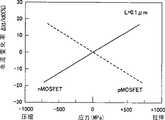
例如了解到,如果在形成MISFET后,改变兼做层间绝缘膜的自调整接触用(self align contact)的等离子CVD氮化膜(通过等离子CVD法形成的氮化膜)的形成条件,则膜中的应力从压缩方向改变为拉伸方向,发生大的变化,由此MISFET的晶体管特性也发生大的变化。这在图2的漏极电流的层间绝缘膜应力依存性中示出。但是,图中的应力值不是表示MISFET的沟道形成区域的内部应力的值,而是从覆盖了层间绝缘膜之后的晶片的翘曲换算求出的层间绝缘膜自身的值。For example, it is known that if the formation conditions of the plasma CVD nitride film (nitride film formed by the plasma CVD method) used as the self-aligning contact (self align contact) of the interlayer insulating film are changed after the MISFET is formed, the film The stress in the MISFET changes greatly from the compressive direction to the tensile direction, and thus the transistor characteristics of the MISFET also change greatly. This is shown in the interlayer insulating film stress dependence of the drain current in FIG. 2 . However, the stress value in the figure does not represent the internal stress of the channel formation region of the MISFET, but is the value of the interlayer insulating film itself calculated from the warpage of the wafer covered with the interlayer insulating film.
由应力产生的影响虽然与上述文献的趋势相同,但其大小增加一位数以上,为±10~20%。还有,显示出在n沟道导电型MISFET与p沟道导电型MISFET中,相对于膜的应力,漏极电流的增减明显相反。The influence due to stress has the same tendency as the above-mentioned literature, but its magnitude increases by more than one digit, and is ±10 to 20%. In addition, it was shown that the increase and decrease of the drain current with respect to the stress of the film are clearly opposite between the n-channel conductivity type MISFET and the p-channel conductivity type MISFET.
因此,当改变层间绝缘膜等的形成条件、内部应力的大小发生变化时,n沟道导电型MISFET及p沟道导电型MISFET的漏极电流表现出相反的动作,存在两元件的漏极电流不能同时增大的问题。Therefore, when the formation conditions of the interlayer insulating film and the like are changed and the magnitude of the internal stress changes, the drain currents of the n-channel conductivity type MISFET and the p-channel conductivity type MISFET show opposite actions, and there is a drain current of the two elements. The current cannot be increased at the same time.
而且,在0.1μm级以下,该应力引起的漏极电流的变化也在±10~20%以上,存在n沟道导电型MISFET和p沟道导电型MISFET的漏极电流的平衡发生变化的问题。Moreover, the change in the drain current due to the stress is also more than ±10 to 20% below the 0.1 μm level, and there is a problem that the balance of the drain current of the n-channel conductivity type MISFET and the p-channel conductivity type MISFET changes. .
本发明的目的在于,提供一种可提高n沟道导电型场效应晶体管及p沟道导电型场效应晶体管的电流驱动能力的技术。An object of the present invention is to provide a technique capable of improving the current drive capability of an n-channel conduction type field effect transistor and a p-channel conduction type field effect transistor.
本发明的另一目的在于,提供一种可抑制n沟道导电型场效应晶体管和p沟道导电型场效应晶体管中的一方的晶体管的电流驱动能力的降低,提高另一方的晶体管的电流驱动能力的技术。Another object of the present invention is to provide a device that can suppress the reduction of the current driving capability of one of the n-channel conductive field effect transistor and the p-channel conductive field effect transistor, and improve the current driving capability of the other transistor. capable technology.
本发明的其他目的和新特征,可根据本说明书的说明及附图明了。Other objects and novel features of the present invention can be clarified from the description of this specification and the accompanying drawings.
如下所述,简单地说明本申请公开的发明中的代表性的概要。A representative summary of the inventions disclosed in the present application will be briefly described as follows.
(1)一种半导体器件,具有在半导体基板的一主面的第1区域构成了沟道形成区域的n沟道导电型场效应晶体管、及在上述半导体基板的一主面的与第1区域不同的第2区域构成了沟道形成区域的p沟道导电型场效应晶体管,在该半导体器件中,(1) A semiconductor device comprising an n-channel conduction type field effect transistor having a channel formation region in a first region of a main surface of a semiconductor substrate, and a first region of a main surface of the above-mentioned semiconductor substrate. The different second region constitutes the p-channel conductivity type field effect transistor of the channel formation region, and in this semiconductor device,
在上述n沟道导电型场效应晶体管的沟道形成区域产生的内部应力是拉伸应力,The internal stress generated in the channel formation region of the above-mentioned n-channel conductivity type field effect transistor is tensile stress,
在上述p沟道导电型场效应晶体管的沟道形成区域产生的内部应力是压缩应力。The internal stress generated in the channel formation region of the p-channel conductivity type field effect transistor is compressive stress.
(2)一种半导体器件,具有在半导体基板的一主面的第1区域构成了沟道形成区域的n沟道导电型场效应晶体管、及在上述半导体基板的一主面的与第1区域不同的第2区域构成了沟道形成区域的p沟道导电型场效应晶体管,在该半导体器件中,(2) A semiconductor device comprising an n-channel conduction type field effect transistor having a channel formation region in a first region of a main surface of a semiconductor substrate, and a first region and a first region of a main surface of the above-mentioned semiconductor substrate. The different second region constitutes the p-channel conductivity type field effect transistor of the channel formation region, and in this semiconductor device,
当在上述n沟道导电型场效应晶体管及上述p沟道导电型场效应晶体管的沟道形成区域产生的内部应力是压缩应力时,在上述p沟道导电型场效应晶体管的沟道形成区域产生的压缩应力,比在上述n沟道导电型场效应晶体管的沟道形成区域产生的压缩应力大。When the internal stress generated in the channel formation region of the above-mentioned n-channel conductivity type field effect transistor and the above-mentioned p-channel conductivity type field effect transistor is compressive stress, in the channel formation region of the above-mentioned p-channel conductivity type field effect transistor The generated compressive stress is larger than the compressive stress generated in the channel formation region of the above-mentioned n-channel conductivity type field effect transistor.
(3)一种半导体器件,具有在半导体基板的一主面的第1区域构成了沟道形成区域的n沟道导电型场效应晶体管、及在上述半导体基板的一主面的与第1区域不同的第2区域构成了沟道形成区域的p沟道导电型场效应晶体管,在该半导体器件中,(3) A semiconductor device comprising an n-channel conduction type field effect transistor forming a channel formation region in a first region of a main surface of a semiconductor substrate, and a first region of a main surface of the above-mentioned semiconductor substrate. The different second region constitutes the p-channel conductivity type field effect transistor of the channel formation region, and in this semiconductor device,
当在上述n沟道导电型场效应晶体管及上述p沟道导电型场效应晶体管的沟道形成区域产生的内部应力是拉伸应力时,在上述n沟道导电型场效应晶体管的沟道形成区域产生的拉伸应力,比在上述p沟道导电型场效应晶体管的沟道形成区域产生的拉伸应力大。When the internal stress generated in the channel formation region of the above-mentioned n-channel conduction type field effect transistor and the above-mentioned p-channel conduction type field effect transistor is tensile stress, the channel formation of the above-mentioned n-channel conduction type field effect transistor The tensile stress generated in the region is larger than the tensile stress generated in the channel formation region of the p-channel conductivity type field effect transistor.
(4)一种半导体器件,具有在半导体基板的一主面的第1区域构成了沟道形成区域的n沟道导电型场效应晶体管、及在上述半导体基板的一主面的与第1区域不同的第2区域构成了沟道形成区域的p沟道导电型场效应晶体管,在该半导体器件中,(4) A semiconductor device comprising an n-channel conduction type field effect transistor having a channel formation region in a first region of a main surface of a semiconductor substrate, and a first region and a first region of a main surface of the above-mentioned semiconductor substrate. The different second region constitutes the p-channel conductivity type field effect transistor of the channel formation region, and in this semiconductor device,
至少具有在上述n沟道导电型场效应晶体管的沟道形成区域产生拉伸应力的膜、及在上述p沟道导电型场效应晶体管的沟道形成区域产生压缩应力的膜中的一个。At least one of a film that generates tensile stress in the channel formation region of the n-channel conductivity type field effect transistor and a film that generates compressive stress in the channel formation region of the p-channel conductivity type field effect transistor.
(5)在上述(4)所记载的半导体器件中,(5) In the semiconductor device described in the above (4),
上述膜是氮化硅系的膜。氮化硅系的膜是通过LP-CVD(低压化学气相淀积)法覆膜的氮化硅(如Si3N4)膜、通过等离子CVD法覆膜的氮化硅(如Si3N4)膜、及通过单片式热CVD法覆膜的氮化硅(如Si3N4)膜。The above-mentioned film is a silicon nitride-based film. The silicon nitride-based film is a silicon nitride (such as Si3 N4 ) film coated by LP-CVD (low pressure chemical vapor deposition), a silicon nitride (such as Si3 N4 ) film coated by plasma CVD ) film, and a silicon nitride (such as Si3 N4 ) film coated by a monolithic thermal CVD method.
(6)在上述(4)所记载的半导体器件中,(6) In the semiconductor device described in (4) above,
在上述n沟道导电型场效应晶体管的沟道形成区域产生拉伸应力的膜,是在上述半导体基板的一主面上以覆盖上述n沟道导电型场效应晶体管的方式形成的膜,The film that generates tensile stress in the channel formation region of the n-channel conductivity type field effect transistor is formed on one main surface of the semiconductor substrate so as to cover the above-mentioned n-channel conductivity type field effect transistor,
在上述p沟道导电型场效应晶体管的沟道形成区域产生压缩应力的膜,是在上述半导体基板的一主面上以覆盖上述p沟道导电型场效应晶体管的方式形成的膜。The film generating compressive stress in the channel formation region of the p-channel conductivity type field effect transistor is formed on one main surface of the semiconductor substrate so as to cover the p-channel conductivity type field effect transistor.
(7)在上述(4)所记载的半导体器件中,(7) In the semiconductor device described in (4) above,
在上述n沟道导电型场效应晶体管的沟道形成区域产生拉伸应力的膜,是在上述n沟道导电型场效应晶体管的栅极电极或上述栅极电极的侧壁形成的侧壁间隔件,The film that generates tensile stress in the channel formation region of the n-channel conductivity type field effect transistor is a sidewall spacer formed on the gate electrode of the above-mentioned n-channel conductivity type field effect transistor or the sidewall of the above-mentioned gate electrode. pieces,
在上述p沟道导电型场效应晶体管的沟道形成区域产生压缩应力的膜,是在上述p沟道导电型场效应晶体管的栅极电极或上述栅极电极的侧壁形成的侧壁间隔件。The film that generates compressive stress in the channel formation region of the p-channel conductivity field effect transistor is a sidewall spacer formed on the gate electrode of the p-channel conductivity field effect transistor or the side wall of the gate electrode. .
(8)一种半导体器件的制造方法,该半导体器件具有在半导体基板的一主面的第1区域构成了沟道形成区域的n沟道导电型场效应晶体管、及在上述半导体基板的一主面的与第1区域不同的第2区域构成了沟道形成区域的p沟道导电型场效应晶体管,在该半导体器件的制造方法中,含有下述工序,(8) A method of manufacturing a semiconductor device comprising an n-channel conduction type field effect transistor having a channel formation region in a first region of a main surface of a semiconductor substrate, and a main surface of the above-mentioned semiconductor substrate. The second region different from the first region on the surface constitutes a p-channel conductivity type field effect transistor in a channel formation region. In the manufacturing method of the semiconductor device, the following steps are included,
在形成上述n沟道导电型场效应晶体管及上述p沟道导电型场效应晶体管之后,至少形成在上述n沟道导电型场效应晶体管的沟道形成区域产生拉伸应力的膜、及在上述p沟道导电型场效应晶体管的沟道形成区域产生压缩应力的膜中的一个膜的工序。After forming the above-mentioned n-channel conductivity type field effect transistor and the above-mentioned p-channel conductivity type field effect transistor, at least a film that generates tensile stress in the channel formation region of the above-mentioned n-channel conductivity type field effect transistor, and a film in the above-mentioned A process of one of the films that generate compressive stress in the channel formation region of the p-channel conductivity type field effect transistor.
(9)在上述(8)所记载的半导体器件中,(9) In the semiconductor device described in the above (8),
上述膜是氮化硅系的膜。The above-mentioned film is a silicon nitride-based film.
(10)一种半导体器件的制造方法,该半导体器件具有在半导体基板的一主面的第1区域构成了沟道形成区域的n沟道导电型场效应晶体管、及在上述半导体基板的一主面的与第1区域不同的第2区域构成了沟道形成区域的p沟道导电型场效应晶体管,在该半导体器件的制造方法中,包含下述工序,(10) A method of manufacturing a semiconductor device comprising an n-channel conduction type field effect transistor having a channel formation region in a first region of a main surface of a semiconductor substrate, and a main surface of the above-mentioned semiconductor substrate. The second region different from the first region on the surface constitutes a p-channel conductivity type field effect transistor in a channel formation region. In the manufacturing method of the semiconductor device, the following steps are included,
形成上述n沟道导电型场效应晶体管及上述p沟道导电型场效应晶体管的工序,The process of forming the above-mentioned n-channel conductivity type field effect transistor and the above-mentioned p-channel conductivity type field effect transistor,
在上述半导体基板的一主面的第1区域及第2区域上,形成在上述p沟道导电型场效应晶体管的沟道形成区域产生压缩应力的绝缘膜的工序,A step of forming an insulating film that generates compressive stress in a channel formation region of the p-channel conductivity type field effect transistor on the first region and the second region of the one main surface of the semiconductor substrate,
在上述半导体基板的一主面的第2区域上的上述绝缘膜有选择地掺入杂质,以缓和在上述n沟道导电型场效应晶体管的沟道形成区域产生的压缩应力的工序。A step of selectively doping the insulating film on the second region of the one main surface of the semiconductor substrate with impurities to relieve the compressive stress generated in the channel formation region of the n-channel conductivity type field effect transistor.
(11)一种半导体器件的制造方法,该半导体器件具有在半导体基板的一主面的第1区域构成了沟道形成区域的n沟道导电型场效应晶体管、及在上述半导体基板的一主面的与第1区域不同的第2区域构成了沟道形成区域的p沟道导电型场效应晶体管,在该半导体器件的制造方法中,包含下述工序,(11) A method of manufacturing a semiconductor device comprising an n-channel conduction type field effect transistor having a channel formation region in a first region of a main surface of a semiconductor substrate, and a main surface of the above-mentioned semiconductor substrate. The second region different from the first region on the surface constitutes a p-channel conductivity type field effect transistor in a channel formation region. In the manufacturing method of the semiconductor device, the following steps are included,
形成上述n沟道导电型场效应晶体管及上述p沟道导电型场效应晶体管的工序,The process of forming the above-mentioned n-channel conductivity type field effect transistor and the above-mentioned p-channel conductivity type field effect transistor,
在上述半导体基板的一主面的第1区域及第2区域上,形成在上述n沟道导电型场效应晶体管的沟道形成区域产生拉伸应力的绝缘膜的工序,A step of forming an insulating film that generates tensile stress in a channel formation region of the n-channel conductivity type field effect transistor on the first region and the second region of the one main surface of the semiconductor substrate,
在上述半导体基板的一主面的第1区域上的上述绝缘膜中有选择地掺入杂质,以缓和在上述p沟道导电型场效应晶体管的沟道形成区域产生的压缩应力的工序。A step of selectively doping impurities into the insulating film on the first region of the one main surface of the semiconductor substrate to relieve compressive stress generated in a channel formation region of the p-channel conductivity type field effect transistor.
以下,说明本发明的要点部分的构成。Hereinafter, the configuration of the main points of the present invention will be described.
本发明的要点是对作用于n沟道导电型场效应晶体管及p沟道导电型场效应晶体管的各沟道形成区域的应力的方向或大小,在各漏极电流增加的方向进行控制。例如如下进行。The gist of the present invention is to control the direction or magnitude of the stress acting on each channel formation region of the n-channel conductivity type field effect transistor and the p-channel conductivity type field effect transistor in the direction in which each drain current increases. For example, it is performed as follows.
1)以使拉伸应力对n沟道导电型场效应晶体管的沟道形成区域产生作用、压缩应力对p沟道导电型场效应晶体管的沟道形成区域产生作用的方式,在n沟道导电型场效应晶体管及p沟道导电型场效应晶体管,改变半导体基板的一主面上形成的膜的材料。1) In such a manner that tensile stress acts on the channel formation region of the n-channel conduction type field effect transistor and compressive stress acts on the channel formation region of the p-channel conduction type field effect transistor, conduction in the n-channel A type field effect transistor and a p-channel conduction type field effect transistor change the material of the film formed on one main surface of the semiconductor substrate.
2)在压缩应力对n沟道导电型场效应晶体管及p沟道导电型场效应晶体管的沟道形成区域产生作用的情况下,以使作用于n沟道导电型场效应晶体管的沟道形成区域的压缩应力,比作用于p沟道导电型场效应晶体管的沟道形成区域的压缩应力小的方式,改变半导体基板的一主面上形成的膜的材料。2) Under the condition that the compressive stress acts on the channel formation regions of the n-channel conduction type field effect transistor and the p-channel conduction type field effect transistor, the channel formation acting on the n-channel conduction type field effect transistor The material of the film formed on one main surface of the semiconductor substrate is changed so that the compressive stress of the region is smaller than the compressive stress applied to the channel formation region of the p-channel conductivity type field effect transistor.
3)在拉伸应力对n沟道导电型场效应晶体管及p沟道导电型场效应晶体管的沟道形成区域产生作用的情况下,以使作用于p沟道导电型场效应晶体管的沟道形成区域的拉伸应力,比作用于n沟道导电型场效应晶体管的沟道形成区域的拉伸应力小的方式,改变在半导体基板的一主面上形成的膜的材料。3) In the case where the tensile stress acts on the channel formation regions of the n-channel conduction type field effect transistor and the p-channel conduction type field effect transistor, so that the channel acting on the p-channel conduction type field effect transistor The material of the film formed on one main surface of the semiconductor substrate is changed so that the tensile stress in the formation region is smaller than the tensile stress applied to the channel formation region of the n-channel conductivity type field effect transistor.
根据上述方法,与通过通常的工艺形成的n沟道导电型场效应晶体管及p沟道导电型场效应晶体管相比,可同时增加n沟道导电型场效应晶体管及p沟道导电型场效应晶体管两者的漏极电流。而且,可以某种程度地自由设定n沟道导电型场效应晶体管及p沟道导电型场效应晶体管的漏极电流。According to the above method, compared with the n-channel conductivity type field effect transistor and the p-channel conductivity type field effect transistor formed by the usual process, the n-channel conductivity type field effect transistor and the p-channel conductivity type field effect transistor can be simultaneously increased. The drain current of both transistors. Furthermore, the drain currents of the n-channel conductivity type field effect transistor and the p-channel conductivity type field effect transistor can be freely set to some extent.
也就是说,分别在n沟道导电型场效应晶体管的沟道形成区域施加拉伸应力、在p沟道导电型场效应晶体管的沟道形成区域施加压缩应力,其结果如图2所示,对应作用于n沟道导电型场效应晶体管及p沟道导电型场效应晶体管的沟道形成区域的应力,漏极电流在n沟道导电型场效应晶体管及p沟道导电型场效应晶体管一起增加。That is to say, tensile stress is applied to the channel formation region of the n-channel conductivity type field effect transistor, and compressive stress is applied to the channel formation region of the p-channel conductivity type field effect transistor. The results are shown in FIG. 2, Corresponding to the stress acting on the channel formation region of the n-channel conduction type field effect transistor and the p-channel conduction type field effect transistor, the drain current in both the n-channel conduction type field effect transistor and the p-channel conduction type field effect transistor Increase.
而且,由于可以分别控制作用于n沟道导电型场效应晶体管及p沟道导电型场效应晶体管的沟道形成区域的应力,所以可以自由控制n沟道导电型场效应晶体管及p沟道导电型场效应晶体管的漏极电流比。Moreover, since the stress acting on the channel formation regions of the n-channel conduction type field effect transistor and the p-channel conduction type field effect transistor can be controlled separately, the n-channel conduction type field effect transistor and the p-channel conduction type field effect transistor can be freely controlled. The drain current ratio of a type field effect transistor.
另外,在这里定义几个术语。Additionally, several terms are defined here.
所谓作用于场效应晶体管的沟道形成区域的拉伸应力,是指在沟道形成区域是硅(Si)的情况下,使Si的晶格常数变为比平衡状态大的应力而言。The tensile stress acting on the channel formation region of the field effect transistor refers to stress that makes the lattice constant of Si larger than the equilibrium state when the channel formation region is silicon (Si).
所谓作用与场效应晶体管的沟道形成区域的压缩应力,是指在沟道形成区域是硅(Si)的情况下,使Si的晶格常数变为比平衡状态小的应力而言。The compressive stress acting on the channel formation region of the field effect transistor refers to the stress that makes the lattice constant of Si smaller than the equilibrium state when the channel formation region is silicon (Si).
所谓膜具有的拉伸应力,是指使在场效应晶体管的沟道形成区域产生拉伸应力而言。The term "tensile stress" of the film refers to the generation of tensile stress in the channel formation region of the field effect transistor.
所谓膜具有的压缩应力,是指使在场效应晶体管的沟道形成区域产生压缩应力而言。The compressive stress of the film refers to generating compressive stress in the channel formation region of the field effect transistor.
因此,本发明的宗旨意味着在沟道形成区域的硅原子的原子间距离,在n沟道导电型场效应晶体管及p沟道导电型场效应晶体管不同,换而言之是偏离的大小不同,还意味着硅原子间距离在n沟道导电型场效应晶体管的沟道形成区域比p沟道导电型场效应晶体管的沟道形成区域大。Therefore, the gist of the present invention means that the interatomic distance of the silicon atoms in the channel formation region is different in the n-channel conduction type field effect transistor and the p-channel conduction type field effect transistor, in other words, the magnitude of the deviation is different. , also means that the distance between silicon atoms is larger in the channel formation region of the n-channel conductivity type field effect transistor than in the channel formation region of the p-channel conductivity type field effect transistor.
附图说明Description of drawings
图1是表示本发明实施例1的半导体器件的概要构成的示意性剖视图。FIG. 1 is a schematic cross-sectional view showing a schematic configuration of a semiconductor device according to
图2是表示电流驱动能力与膜应力的关系的特性图。FIG. 2 is a characteristic diagram showing the relationship between current driving capability and film stress.
图3是制造图1的半导体器件的工艺((a)、(b)和(c)是示意性剖视图)。FIG. 3 is a process of manufacturing the semiconductor device of FIG. 1 ((a), (b) and (c) are schematic cross-sectional views).
图4是制造本发明实施例2的半导体器件的工艺((a)、(b)、(c)和(d)是示意性剖视图)。Fig. 4 is a process of manufacturing the semiconductor device of
图5是制造本发明实施例3的半导体器件的工艺((a)、(b)和(c)是示意性剖视图)。Fig. 5 is a process of manufacturing the semiconductor device of
图6是制造本发明实施例4的半导体器件的工艺((a)、(b)和(c)是示意性剖视图)。Fig. 6 is a process of manufacturing the semiconductor device of
图7是表示本发明实施例5的半导体器件的概要构成的示意性剖视图。7 is a schematic cross-sectional view showing a schematic configuration of a semiconductor device according to
图8是表示本发明实施例6的半导体器件的概要构成的示意性剖视图。8 is a schematic cross-sectional view showing a schematic configuration of a semiconductor device according to
图9是表示本发明实施例7的半导体器件的概要构成的示意性剖视图。9 is a schematic cross-sectional view showing a schematic configuration of a semiconductor device according to
图10是表示本发明实施例8的半导体器件的概要构成的示意性剖视图。10 is a schematic cross-sectional view showing a schematic configuration of a semiconductor device according to
图11是表示在本发明实施例3的半导体器件的制造中的倾斜注入工序的示意性剖视图。11 is a schematic cross-sectional view showing an oblique implantation step in the manufacture of the semiconductor device according to
具体实施方式Detailed ways
以下,参照附图详细说明本发明的实施方式。并且,在用于说明本发明的实施方式的全部附图中,具有相同功能的附带相同图号,并省略对其的重复说明。Hereinafter, embodiments of the present invention will be described in detail with reference to the drawings. In addition, in all the drawings for explaining the embodiments of the present invention, those having the same functions are assigned the same reference numerals, and their repeated descriptions are omitted.
(实施例1)(Example 1)
在本发明的实施例1中,说明在具有电源电压为1~1.5V、栅极长度为0.1~0.14μm的互补型MISFET的半导体器件中运用本发明的实例。In
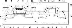
图1是表示本发明实施例1的半导体器件的概要构成的示意性剖视图,图2是表示电流驱动能力与膜应力的关系的特性图,图3是制造图1的半导体器件的工艺((a)、(b)和(c)是示意性剖视图)。在图1及图3中,左侧的是n沟道导电型MISFET,右侧的是p沟道导电型MISFET。1 is a schematic cross-sectional view showing the schematic structure of the semiconductor device of
本实施例的半导体器件如图1所示,半导体基板以例如由单晶硅构成的p型硅基板1为主体构成。p型硅基板1的电路形成面(一主面)具有第1元件形成区域及第2元件形成区域,该第1元件形成区域及第2元件形成区域通过元件间绝缘分离区域如浅槽隔离(SGI:Shallow Groove Isolation)区域4被相互划分。在第1元件形成区域中形成p型阱区域2及n沟道导电型MISFET,在第2元件形成区域中形成n型阱区域3及p沟道导电型MISFET。浅槽隔离区域4如下形成:在p型硅基板1的电路形成面形成浅槽,然后在浅槽的内部有选择地埋入绝缘膜(例如氧化硅膜)。In the semiconductor device of this embodiment, as shown in FIG. 1 , the semiconductor substrate is mainly composed of a p-
n沟道导电型MISFET的构成为,主要具有沟道形成区域、栅极绝缘膜5、栅极电极6、侧壁间隔件9、源区及漏区。源区及漏区的构成为,具有n型半导体区域(扩展区域)7及n型半导体区域10。n型半导体区域7通过相对栅极电极6自调整而形成,n型半导体区域10通过相对设置在栅极电极6的侧壁的侧壁间隔件9自调整而形成。n型半导体区域10形成为比n型半导体区域7的杂质浓度高。The configuration of the n-channel conductivity type MISFET mainly includes a channel formation region, a
p沟道导电型MISFET的构成为,主要具有沟道形成区域、栅极绝缘膜5、栅极电极6、侧壁间隔件9、源区及漏区。源区及漏区的构成为,具有p型半导体区域(扩展区域)8及p型半导体区域11。p型半导体区域8通过相对栅极电极6自调整而形成,p型半导体区域11通过相对设置在栅极电极6的侧壁的侧壁间隔件9自调整而形成。p型半导体区域11形成为比p型半导体区域8的杂质浓度高。The configuration of the p-channel conductivity type MISFET mainly includes a channel formation region, a
在栅极电极6、n型半导体区域10、p型半导体区域11的各表面上,形成用于实现低电阻化的硅化物层(金属半导体反应层)12。在p型硅基板1的电路形成面上,形成例如由氧化硅膜构成的层间绝缘膜15。On the respective surfaces of the
在n沟道导电型MISFET和层间绝缘膜15之间,形成第1氮化膜例如氮化硅膜13,作为在p型硅基板1的电路形成面产生拉伸应力的膜。在p沟道导电型MISFET和层间绝缘膜15之间,形成第2氮化膜例如氮化硅膜14,作为在p型硅基板1的电路形成面产生压缩应力的膜。在本实施例中,氮化硅膜13在p型硅基板1的电路形成面上有选择地形成为覆盖n沟道导电型MISFET,氮化硅膜14在p型硅基板1的电路形成面上有选择地形成为覆盖p沟道导电型MISFET。Between the n-channel conductivity type MISFET and the
氮化硅膜13及14例如通过等离子CVD法而形成。该氮化硅膜13及14通过可改变其形成条件(反应气体、压力、温度、高频功率),可控制在p型硅基板1的电路形成面上产生的应力。在本实施例中,氮化硅膜13是例如在膜形成时的高频功率低功率化为300~400W,在拉伸方向控制在p型硅基板1的电路形成面上产生的应力的膜。氮化硅膜14是例如在膜形成时的高频功率低功率化为600~700W,在压缩方向控制在p型硅基板1的电路形成面上产生的应力的膜。The
由于在如上形成的氮化硅膜13中大致存在+700~+800Mpa的拉伸应力,在氮化硅膜14中大致存在-900~-1000Mpa的压缩应力,所以在n沟道导电型MISFET的沟道形成区域产生拉伸应力,在p沟道导电型MISFET的沟道形成区域产生压缩应力。其结果如图2所示,与没有覆盖氮化硅膜13及14的情况比较,n沟道导电型MISFET的漏极电流提高10~15%,p沟道导电型MISFET的漏极电流提高15~20%。而且,如上所述,这些应力的方向与沟道形成区域的漏极电流(Id)的流动方向(栅极长度方向)相同。Since the
接下来,利用图3说明本实施例1的半导体器件的制造方法。Next, a method of manufacturing the semiconductor device of the first embodiment will be described using FIG. 3 .
首先,准备由具有比电阻为10Ωcm的单晶硅构成的p型硅基板1(以下简称为p型基板),然后,在p型硅基板1的电路形成面上有选择地形成p型阱区域2及n型阱区域3。First, a p-type silicon substrate 1 (hereinafter simply referred to as a p-type substrate) made of single crystal silicon having a specific resistance of 10 Ωcm is prepared, and then a p-type well region is selectively formed on the circuit formation surface of the p-
然后,在p型基板1的电路形成面上形成浅槽隔离区域4,作为划分第1元件形成区域及第2元件形成区域的元件间隔离区域。这个浅槽隔离区域4如下形成:在p型基板1的电路形成面上形成浅槽(例如大致为300nm深度的槽),然后,在p型基板1的电路形成面上通过CVD法形成例如由氧化硅膜形成的绝缘膜,然后,为使绝缘膜只存在于浅槽内部而通过CMP(化学机械研磨:Chemical MechanicalPolishing)法平坦化。Then, a shallow
然后,实施热处理,在p型基板1的电路形成面的元件形成区域,形成例如由厚度大致为2~3nm的氧化硅膜构成的栅极绝缘膜5,然后,通过CVD法在p型基板1的电路形成面上的全面形成例如厚度大致为150~200nm的多晶硅膜,然后,在多晶硅膜上实施布图而形成栅极电极6。在多晶硅膜上,降低电阻值的杂质在堆积中或堆积后掺入。Then, a heat treatment is performed to form a
然后,在没有形成栅极电极6的p型阱区域2的部分,通过离子注入法有选择地掺入例如作为杂质的砷(As),形成一对n型半导体区域(扩展区域)7,然后,在没有形成栅极电极6的n型阱区域3的部分,通过离子注入法有选择地掺入例如作为杂质的二氟化硼(BF2),形成一对p型半导体区域(扩展区域)8。n型半导体区域7的形成,在使用光抗蚀剂膜覆盖了DMIS形成区域的状态下进行。而且,p型半导体区域8的形成,在使用光抗蚀剂膜覆盖了nMIS形成区域的状态下进行。砷的掺入在加速能量为1~5KeV、掺杂量为1~2×10¹⁵/cm2的条件下进行。而且,二氟化硼的掺入在加速能量为1~5KeV、掺杂量为1~2×1015/cm2的条件下进行。到此为止的工序如图3(a)所示。Then, in the part of the p-
然后,如图3(b)所示,在栅极电极6的侧壁形成栅极长度方向的膜厚大致为50~70nm的侧壁间隔件9。侧壁间隔件9如下形成:通过CVD法在p型基板1的电路形成面上的全面形成由氧化硅膜或氮化硅膜形成的绝缘膜,然后在绝缘膜上实施RIE(反应离子腐蚀:Reactive Ion Etching)等各向异性的腐蚀。Then, as shown in FIG. 3( b ),
然后,在没有形成栅极电极6及侧壁间隔件9的p型阱区域2的部分,通过离子注入法有选择地掺入例如作为杂质的砷(As),形成一对n型半导体区域(扩展区域)10,然后,在没有形成栅极电极6及侧壁间隔件9的n型阱区域3的部分,通过离子注入法有选择地掺入例如作为杂质的二氟化硼(BF2),形成一对p型半导体区域(扩展区域)11。n型半导体区域10的形成,在使用光抗蚀剂膜覆盖了pMIS形成区域的状态下进行。而且,p型半导体区域11的形成,在使用光抗蚀剂膜覆盖了nMIS形成区域的状态下进行。砷的掺入在加速能量为35~45KeV、掺杂量为2~4×10¹⁵/cm2的条件下进行。而且,二氟化硼的掺入在加速能量为40~50KeV、掺杂量为2~4×1015/cm2的条件下进行。Then, in the portion of the p-
在这个工序中,形成由n型半导体区域7及n型半导体区域10构成的源区及漏区。而且,形成由p型半导体区域8及n型半导体区域11构成的源区及漏区。In this step, a source region and a drain region composed of n-
然后,除去自然的氧化膜以露出栅极电极6及半导体区域(10、11)的表面后,通过溅射法在含有上述这些表面的p型基板1的电路形成面上全面形成作为高熔点金属膜的如钴(Co)膜,然后,实施热处理,使栅极电极6的硅(Si)与钴膜的Co发生反应,在栅极电极6的表面形成硅化物(CoSix)层12,同时使半导体区域(10、11)的Si与钴膜的Co发生反应,在半导体区域的表面形成硅化物(CoSix)层12,然后,有选择地除去形成了硅化物层12区域以外的未反应的钴膜,然后,实施热处理使硅化物膜12活性化。Then, after removing the natural oxide film to expose the surface of the
然后,在p型基板1的电路形成面上的整个面上,通过等离子CVD法形成例如作为绝缘膜的厚度大致为100~120nm的氮化硅膜13。氮化硅膜13的形成,在例如高频功率350~400W、或炉内压力为300~350Torr的条件下进行。Then, a
然后,利用光刻技术在氮化硅膜13上实施布图,如图3(c)所示,有选择地形成覆盖n沟道型导电型MISFET的氮化硅膜13。即,除去在p沟道导电型MISFET上的氮化硅膜13。如上所述形成的氮化硅膜13,可有选择地在n沟道导电型MISFET的沟道形成区域产生拉伸应力。Then, patterning is carried out on the
然后,在p型基板1的电路形成面上的全面,通过等离子CVD法形成例如作为绝缘膜的厚度大致为100nm的氮化硅膜14。氮化硅膜14的形成,在例如高频功率600~700W、或炉内压力为5~10Torr的条件下进行。Then, a
然后,利用光刻技术在氮化硅膜14上实施布图,如图3(c)所示,有选择地形成覆盖p沟道型导电型MISFET的氮化硅膜14。即,除去在n沟道导电型MISFET上的氮化硅膜14。如上所述形成的氮化硅膜14,可在p沟道导电型MISFET的沟道形成区域产生压缩应力。Then, patterning is carried out on the
然后,通过等离子CVD法,在p型基板1的电路形成面上的全面形成例如由氧化硅膜构成的层间绝缘膜15,然后,通过CMP法使层间绝缘膜15的表面平坦化。然后,利用公知技术形成接触孔、金属布线层。Then, an
关于氮化硅膜13及14的加工方法,使用各向同性的干法腐蚀或湿法腐蚀。虽然在各向异性的干法腐蚀的情况下,在栅极台阶部残留氮化硅膜,应力效果多少减弱,但是这样也可以。As for the processing method of the
在本实施例1中,通过直接与栅极电极6连接的氮化硅膜控制应力,所以效率最好。特别是在源区及漏区的杂质活性化等的高温热处理结束后,形成用于控制应力的氮化硅膜,所以膜应力几乎可以不变地保留。再有,由于在提高电流驱动能力的同时,可以除去在大的隔离区域的氮化硅膜,所以可以降低隔离区域的寄生电容。氮化硅膜与氧化硅膜相比介电常数高。In the first embodiment, the stress is controlled by the silicon nitride film directly connected to the
另外,在本实施例1中,也可以省略氮化硅膜14。当然,提高p沟道导电型MISFET的电流驱动能力的效果会变小,但可以简化这部分的制造工序。而且,氮化硅膜13也可以通过单片式热CVD法形成,也可以使氮化硅膜13及14同时产生压缩应力或拉伸应力,只是它们的大小不同。In addition, in the first embodiment, the
总之,本实施例1的要点是在漏极电流增加的方向,使在n沟道导电型及p沟道导电型MISFET中至少一方的沟道形成区域发生应力的趋势和大小发生改变。In short, the gist of
而且,在本实施例1中,当设定氮化硅膜13的厚度为较厚时,可防止加工氮化硅膜14时过腐蚀引起的膜厚的减少。而且,两个膜的厚度并没有任何规定。Furthermore, in the first embodiment, when the thickness of the
再有,改变氮化硅膜的形成方法以改变膜应力的方法,除上述实施例的改变高频功率的方法之外,还可以例举以下方法:Furthermore, the method of changing the formation method of the silicon nitride film to change the film stress, in addition to the method of changing the high-frequency power of the above-mentioned embodiment, the following methods can also be exemplified:
1)改变原料气体的方法,在氮化硅膜13的形成中使用SiH4和NH3和N2,在氮化硅膜14的形成中除去NH3使用SiH4和N2。1) A method of changing the source gas, using SiH4 , NH3 and N2 in the formation of the
2)改变温度的方法,与形成氮化硅膜14时相比,形成氮化硅膜13时的温度高。2) In the method of changing the temperature, the temperature at the time of forming the
3)改变压力的方法,与形成氮化硅膜14时相比,形成氮化硅膜13时的压力大。3) In the method of changing the pressure, the pressure at the time of forming the
当然,也可以是上述的任意组合。要点是无论如何要在拉伸应力侧生成氮化硅膜13,在压缩应力侧生成氮化硅膜14。Of course, any combination of the above may also be used. The point is to form the
另外,作为使用单片式热CVD法形成氮化膜的方法,可降低膜形成时的压力、提高温度,而在拉伸侧产生膜应力,适于氮化硅膜13。In addition, as a method of forming a nitride film using a single-wafer thermal CVD method, the pressure at the time of film formation can be lowered, the temperature can be raised, and film stress can be generated on the stretching side, which is suitable for the
(实施例2)(Example 2)
本实施例2目标在于简化上述实施例1的制造工序。图4是制造本发明实施例2的半导体器件的工艺((a)、(b)、(c)和(d)是示意性剖视图)。The second embodiment is aimed at simplifying the manufacturing process of the above-mentioned first embodiment. Fig. 4 is a process of manufacturing the semiconductor device of
如图4所示,通过与上述实施例1相同的工艺,形成n沟道导电型及p沟道导电型MISFET及硅化物层12。As shown in FIG. 4 , n-channel and p-channel conductivity MISFETs and the
然后,在p型基板1的电路形成面上的全面,利用等离子CVD法,形成作为绝缘膜的如厚度大致为100~200nm的氮化硅膜13。氮化硅膜13的形成在如高频功率为350~400W的条件下进行。Then, on the entire surface of the p-
然后,在p型基板1的电路形成面上的全面,形成作为绝缘膜的氧化硅膜13A。该氧化硅膜13A例如是P-TEOS或O3-TEOS氧化膜。Then, a
然后,利用光刻技术顺次在氧化硅膜13A及氮化硅膜13上进行布图,如图4(b)所示,形成有选择地覆盖n沟道导电型MISFET的氮化硅膜13及氧化硅膜13A。即,除去p沟道导电型MISFET上的氮化硅膜13及氧化硅膜13A。这样形成的氮化硅膜13可以在n沟道导电型MISFET的沟道形成区域选择地产生拉伸应力。Then, the
然后,如图4(c)所示,在p型基板1的电路形成面上的全面,利用等离子CVD法,形成作为绝缘膜的如大致100nm厚的氮化硅膜14。氮化硅膜14的形成在如高频功率为350~400W的条件下进行。Then, as shown in FIG. 4( c ), a
然后,利用光刻技术在氧化硅膜14上进行布图,如图4(d)所示,形成有选择地覆盖p沟道导电型MISFET的氮化硅膜14。即,除去n沟道导电型MISFET上的氮化硅膜14。这样形成的氮化硅膜14可以在p沟道导电型MISFET的沟道形成区域选择地产生压缩应力。在这个工序中,氧化硅膜13A成为氮化硅膜14加工时的阻蚀膜。即,可以控制由氮化硅膜14加工时的过蚀引起的氮化硅膜13的薄膜化。Then, patterning is performed on the
然后,如图4(d)所示,在p型基板1的电路形成面上的全面,利用等离子CVD法,形成例如由氧化硅膜构成的层间绝缘膜15,然后,利用CMP法,使层间绝缘膜15的表面平坦化。这之后,利用公知技术形成接触孔、金属布线层而完成。Then, as shown in FIG. 4( d), on the entire surface of the circuit formation surface of the p-
根据本实施例2,在上述实施例1效果的基础上,可提高加工氮化硅膜14的控制性。其结果,可使氮化硅膜13及14的膜厚均匀且薄。According to the second embodiment, in addition to the effects of the first embodiment described above, the controllability of processing the
(实施例3)(Example 3)
本实施例3说明在具有电源电压大致为1~1.5V、栅极长度大致为0.1~0.14μm的互补型MISFET的半导体器件中运用本发明的例。This third embodiment describes an example in which the present invention is applied to a semiconductor device having a complementary MISFET having a power supply voltage of approximately 1 to 1.5 V and a gate length of approximately 0.1 to 0.14 μm.
本实施例3的目标在于简化上述实施例1的制造工序。图5是制造本发明实施例3的半导体器件的工艺((a)、(b)和(c)是示意性剖视图)。在图5中,左侧是n沟道导电型MISFET,右侧是p沟道导电型MISFET。The purpose of this third embodiment is to simplify the manufacturing process of the above-mentioned first embodiment. Fig. 5 is a process of manufacturing the semiconductor device of
如图5所示,在通过与上述实施例1相同的工艺,形成n沟道导电型及p沟道导电型MISFET及硅化物层12后,在p型基板1的电路形成面上的全面,通过等离子CVD法,形成作为绝缘膜的在p沟道导电型MISFET的沟道形成区域产生压缩应力的氮化硅膜16。氮化硅膜16的形成是在例如高频功率为350~400W的条件下进行的。As shown in FIG. 5, after forming the n-channel conductivity type and p-channel conductivity type MISFET and the
然后,在p型基板1的电路形成面上形成抗蚀膜R,该抗蚀膜R覆盖在p沟道导电型MISFET上,且在n沟道导电型MISFET上有开口,然后,如图5(b)所示,把抗蚀膜R作为杂质掺入用掩膜使用,在从抗蚀膜R露出的氮化硅膜16中,采用离子注入法掺入Ar、Ge、Si、As、Sb、In、BF2等杂质。而且,图号17是掺入了这些杂质的氮化硅膜。Then, a resist film R is formed on the circuit formation surface of the p-
然后,除去抗蚀膜R,之后如图5(c)所示,在p型基板1的电路形成面上的全面,利用等离子CVD法形成例如由氧化硅膜构成的层间绝缘膜15,然后通过CMP法使层间绝缘膜15的表面平坦化。然后,利用公知技术形成接触孔、金属布线层而完成。Then, the resist film R is removed, and then, as shown in FIG. The surface of the
这样得到的p沟道导电型MISFET上的氮化硅膜16具有-800~-1000Mpa的压缩应力,在p沟道导电型MISFET的沟道形成区域产生压缩应力。另一方面,n沟道导电型MISFET上的氮化硅膜17的应力显著缓和,几乎成为0的状态。即,在n沟道导电型MISFET的沟道形成区域中的压缩应力被缓和。其结果,与没有覆盖氮化硅膜16的情况比较,p沟道导电型MISFET的漏极电流提高15~20%。这时,n沟道导电型MISFET的漏极电流与使用了高压缩应力的氮化硅膜16无关,几乎不下降。The
这是由于氮化硅膜16中的结晶性因离子注入的冲击而被破坏。因此,当观察氮化硅膜的剖面时,明显地留下被破坏的痕迹。并且,在本实施例中,虽然只在n沟道导电型MISFET上的氮化硅膜中掺入杂质,但如果明确的缓和效果中存在差,则杂质自身也可以存在于n、p沟道导电型MISFET上的两者中。但是,这时需要n沟道导电型MISFET上的氮化硅膜中的杂质量大、或因离子注入而被破坏的区域大。而且,这个破坏区域的大小即应力缓和效果不仅受掺入的杂质的浓度影响,而且还受能量大小的变大左右。例如,在本实施例中,即使仅仅是被掺入n沟道导电型MISFET上的氮化硅膜中的杂质的能量比被掺入p沟道导电型MISFET上的氮化硅膜中的杂质的能量大,也可得到同样的效果。并且,被掺入的杂质的大部分存在于氮化硅膜16中较佳。这是因为有时离子注入的损伤对下部的MISFET施以不良影响。This is because the crystallinity in the
而且,本实施例在氮化硅膜16的覆膜、及选择的离子注入工序后,到元件完成为止之间的热处理工序,700℃是最高温度。如果在这种程度的比较低温的热处理中,因离子注入而被破坏的氮化硅膜几乎不会发生再次结晶。因此,离子注入后的应力的状态在元件制成后也作为残留应力大致维持着。In addition, in this embodiment, after the coating of the
根据本实施例3,通过向氮化硅膜16进行的杂质的离子注入,可以缓和膜中的应力或者相反,通过本实施例也可得到与实施例1相同的效果。这样一来,与上述实施例1比较,由于氮化硅膜的覆膜工序一次完成,所以可省略第2氮化硅膜的覆膜工序及其加工工序,可以简化制造工序。当然,因离子注入可改变膜应力,在p沟道导电型MISFET侧也可以。这时,在p型基板1的电路形成面上的全面,形成在n沟道导电型MISFET的沟道形成区域产生拉伸应力的氮化硅膜,然后,在p沟道导电型MISFET上的氮化硅膜中,通过离子注入法有选择地掺入上述杂质。而且,作为在氮化硅膜中离子注入的离子(杂质),比较重的离子一方通过低浓度离子注入可提高本效果,且效率高,但并不限于何种离子。According to the third embodiment, the ion implantation of impurities into the
而且,虽然作为本实施例中的缓和应力用的离子注入,说明为适用相对硅基板(晶片)垂直的离子注入的情况,但如图11(示意性剖面图)所示,也可以使用倾斜注入。这时,也可在覆盖MISFET的栅极电极的氮化硅膜16的栅极侧壁部分(台阶部分)掺入杂质。其结果,可以得到更好的缓和应力的效果。Furthermore, although ion implantation perpendicular to the silicon substrate (wafer) is applied as ion implantation for stress relaxation in this embodiment, it is also possible to use oblique implantation as shown in FIG. 11 (schematic sectional view). . In this case, impurities may also be doped into the gate side wall portion (step portion) of the
(实施例4)(Example 4)
本实施例4是本发明的本实施例1的半导体器件的制造方法的变形例。对此,使用图6((a)、(b)及(c)的示意剖面图)进行说明。
如图6(a)所示,采用与上述实施例1相同的工艺,形成n沟道导电型MISFET及p沟道导电型MISFET及硅化物层12。As shown in FIG. 6( a ), the n-channel conductivity type MISFET, the p-channel conductivity type MISFET and the
然后,在p型基板1的电路形成面上的全面,利用等离子CVD法形成作为绝缘膜的例如大致膜厚为100~120nm的氮化硅膜13。氮化硅膜13的形成是在例如高频功率为350~400W的条件下进行。Then, a
然后,采用光刻技术在氮化硅膜13上进行布图,如图6(b)所示,形成有选择地覆盖n沟道导电型MISFET的氮化硅膜13。即,除去在p沟道导电型MISFET上的氮化硅膜13。这样形成的氮化硅膜13可以在n沟道导电型MISFET的沟道形成区域选择地产生拉伸应力。Then, patterning is carried out on the
然后,如图6(c)所示,在p型基板1的电路形成面上的全面,利用作为绝缘膜的例如大致膜厚为100~120nm的氮化硅膜14。氮化硅膜14的形成是在例如高频功率为600~700W的条件下进行。Then, as shown in FIG. 6( c ), a
然后,在p型基板1的电路形成面上的全面,利用等离子CVD法形成例如由氧化硅膜构成的层间绝缘膜15,然后采用CMP法使层间绝缘膜15的表面平坦化。之后,采用公知技术形成接触孔、金属布线层而完成。Next, an
在本实施例4中,在p沟道导电型MISFET上只存在氮化硅膜14。另一方面,在n沟道导电型MISFET上存在氮化硅膜13及14。其结果,虽然在p沟道导电型MISFET的沟道形成区域产生大的压缩应力,但在n沟道导电型MISFET的沟道形成区域产生的应力被缓和。在本实施例中,与没有覆盖氮化硅膜的情况比较,可仅使p沟道导电型MISFET的漏极电流提高15~20%。这时,n沟道导电型MISFET的漏极电流几乎不发生变化。In
并且,也可以在主要使n沟道导电型MISFET的漏极电流增加的情况下,先在p沟道导电型MISFET上选择地形成氮化硅膜14,然后在全面形成氮化硅膜13。In addition, in the case of mainly increasing the drain current of the n-channel conductivity type MISFET, the
将本实施例的工序与实施例1和2进行比较,利用光刻除去n沟道导电型MISFET上的氮化硅膜14的工序被省略。其结果,比实施例1和2更简化。Comparing the steps of this embodiment with those of
并且,在实施例中,通过改变氮化硅膜13及14的膜厚及其膜应力的大小,可以同时提高n沟道导电型及p沟道导电型MISFET的漏极电流。例如,在本实施例中,通过使氮化硅膜13的厚度为130~150nm,使氮化硅膜14的膜厚为50~80nm,通过氮化硅膜14提高n沟道导电型MISFET的漏极电流的效果一点也不变小。Moreover, in the embodiment, by changing the film thickness and the film stress of the
(实施例5)(Example 5)
图7是表示本发明实施例5的半导体器件的概要构成的示意性剖视图,图中的23是具有拉伸应力的涂敷氧化膜(SOG:Spin On Glass)。7 is a schematic cross-sectional view showing a schematic configuration of a semiconductor device according to
本实施例5的半导体器件是改变控制应力的膜、构造的器件,是上述应用例的任意组合。例如,如图7所示,在含有栅极电极6正上方的p型基板1的电路形成面的全面,形成自调整接触工艺用的具有压缩应力的氮化硅膜19,然后在氮化硅膜19上形成具有拉伸应力的SOG膜23,然后在SOG膜23上进行布图,在n沟道导电型MISFET上有选择地剩余SOG膜23。在n沟道导电型MISFET侧,通过SOG膜23的拉伸应力抵消氮化硅膜19的压缩应力。The semiconductor device of the fifth embodiment is a device in which the film and structure for controlling stress are changed, and is any combination of the above-mentioned application examples. For example, as shown in FIG. 7, a
(实施例6)(Example 6)
图8是表示本发明实施例6的半导体器件的概要构成的示意性剖视图,图中的20是由具有压缩应力的氮化硅膜构成的侧壁间隔件,21是具有拉伸应力的栅极电极,22是具有压缩应力的栅极电极。8 is a schematic cross-sectional view showing a schematic configuration of a semiconductor device according to
本实施例6的半导体器件是如图8所示的器件,其可改变控制上述应力的膜、构造,将上述实施例1中的侧壁间隔件9改变为由具有压缩应力的氮化硅膜构成的侧壁间隔件20,而且,将栅极电极6改变为由具有拉伸应力的材料构成的栅极电极21,或将栅极电极6改变为由具有压缩应力的材料构成的栅极电极22(包括构造改变),通过组合控制应力。The semiconductor device of this
例如,作为上述改变控制上述应力的膜、构造的器件,可以列举通过栅极电极6的材料的改变的组合来控制应力的情况的一例,特别在一个栅极电极6中多掺入杂质(Ge、Si)。而且,栅极电极6也可以是多金属结构。For example, as the above-mentioned device that changes the film and structure that control the above-mentioned stress, an example of the situation that the stress is controlled by the combination of the change of the material of the
而且,作为可改变控制应力的膜、构造的器件,也可以在n沟道导电型MISFET、p沟道导电型MISFET改变栅极绝缘膜材料。例如,n沟道导电型MISFET及p沟道导电型MISFET的任意一方,使用氮化硅膜和氧化硅膜的积层膜。Furthermore, as a device in which the film and structure for controlling stress can be changed, the material of the gate insulating film can also be changed for n-channel conductivity type MISFET and p-channel conductivity type MISFET. For example, either an n-channel conductivity type MISFET or a p-channel conductivity type MISFET uses a laminated film of a silicon nitride film and a silicon oxide film.
(实施例7)(Example 7)
图9是表示本发明实施例7的半导体器件的概要构成的示意性剖视图。虽然本实施例的半导体器件如图9所示,作为可改变控制应力的膜、构造的器件,与上述实施例1一样使用作为层间绝缘膜的一部分的氮化硅膜,但不直接形成氮化硅膜13及氮化硅膜14,该氮化硅膜13在n沟道导电型MISFET的栅极电极6上具有拉伸应力,该氮化硅膜14在p沟道导电型MISFET的栅极电极6上具有拉伸应力,在使层间绝缘膜15的表面平坦化后,形成在p沟道导电型MISFET的栅极电极6上的层间绝缘膜15上具有拉伸应力的氮化硅膜24,形成在p沟道导电型MISFET的栅极电极6上的层间绝缘膜15上具有压缩应力的氮化硅膜25。9 is a schematic cross-sectional view showing a schematic configuration of a semiconductor device according to
在这种结构的情况下,一方的氮化硅膜的除去变得容易。In the case of such a structure, removal of one silicon nitride film becomes easy.
(实施例8)(Embodiment 8)
图10是表示本发明实施例8的半导体器件的概要构成的示意性剖视图。10 is a schematic cross-sectional view showing a schematic configuration of a semiconductor device according to
本实施例8的半导体器件是使用了SOI(Silicon On Insulator)基板30的SOI构造。SOI基板30例如如下构成:具有支持基板30A、设在该支持基板30A上的绝缘层30B、及设在该绝缘层30B上的半导体层30C。支持基板30A例如通过由单晶硅构成的p型硅基板形成,绝缘层30B例如由氧化硅膜形成,半导体层30C例如通过由单晶硅构成的p型半导体形成。半导体层30C被分成多个元件形成部,在各元件形成部形成n沟道导电型MISFET或p沟道导电型MISFET。在形成了n沟道导电型MISFET的半导体层30C的元件形成部形成p型阱区域,在形成了p沟道导电型MISFET的半导体层30C的元件形成部形成n型阱区域。The semiconductor device of the eighth embodiment has an SOI structure using an SOI (Silicon On Insulator)
SOI构造因半导体层30C的厚度薄,故应力的效果更大。而且,在SOI构造的情况下,可通过改变绝缘层(埋层)30B的厚度、或选择地向绝缘层30B掺入杂质,来进行应力的控制。其结果,达成本发明的效果同时,还可以得到SOI构造的优点。In the SOI structure, since the thickness of the semiconductor layer 30C is thin, the effect of the stress is greater. Furthermore, in the case of the SOI structure, stress can be controlled by changing the thickness of the insulating layer (buried layer) 30B or by selectively doping the insulating layer 30B with impurities. As a result, the advantages of the SOI structure can be obtained while achieving the effects of the present invention.
而且,在含有SRAM(静态存储器)、DRAM(动态存储器)、闪存等存储器的产品中,当至少在其存储单元的外围电路或逻辑电路部分使用本发明的构造时,可得到更高性能的存储器产品。Moreover, in products containing memories such as SRAM (static memory), DRAM (dynamic memory), flash memory, etc., when the structure of the present invention is used at least in the peripheral circuit or logic circuit part of its storage unit, a memory with higher performance can be obtained product.
以上,基于上述实施例,具体说明了本发明人进行的发明,但本发明并不限于上述实施例,当然可以在不超出其宗旨的范围内进行种种改变。As mentioned above, the invention made by this inventor was concretely demonstrated based on the said Example, However, this invention is not limited to the said Example, Of course, various changes are possible within the range which does not deviate from the summary.
如简单地说明由本发明公开的代表例得到的效果,则如下所述。The effects obtained by the representative examples disclosed in the present invention will be briefly described as follows.
根据本发明,可提高n沟道导电型场效应晶体管及p沟道导电型场效应晶体管的电流驱动能力。According to the present invention, the current driving capability of the n-channel conduction type field effect transistor and the p-channel conduction type field effect transistor can be improved.
另外,根据本发明,可以抑制n沟道导电型场效应晶体管及p沟道导电型场效应晶体管中一个晶体管的电流驱动能力的降低,可提高另一个晶体管的电流驱动能力。Also, according to the present invention, it is possible to suppress reduction in the current drive capability of one of the n-channel conduction type field effect transistor and the p-channel conduction type field effect transistor, and to improve the current drive capability of the other transistor.
另外,由于可以分别控制作用于n沟道导电型场效应晶体管及p沟道导电型场效应晶体管的沟道形成区域的应力,所以可某种程度自由地设定n沟道导电型场效应晶体管及p沟道导电型场效应晶体管的漏极电流比。In addition, since the stress acting on the channel formation region of the n-channel conductivity type field effect transistor and the p-channel conductivity type field effect transistor can be controlled separately, the n-channel conductivity type field effect transistor can be set freely to some extent. And the drain current ratio of the p-channel conduction type field effect transistor.
产业上的可利用性Industrial availability
如上所述,本发明涉及的半导体器件,应用于具有n沟道导电型场效应晶体管及p沟道导电型场效应晶体管的半导体器件是有益的,另外,应用于存储器集成电路、逻辑集成电路、或具有存储功能及逻辑功能的混合集成电路等半导体器件是有用的。As mentioned above, the semiconductor device related to the present invention is beneficial to be applied to semiconductor devices having n-channel conduction type field effect transistors and p-channel conduction type field effect transistors. In addition, it is beneficial to be applied to memory integrated circuits, logic integrated circuits, It is useful as a semiconductor device such as a hybrid integrated circuit having a memory function and a logic function.
Claims (40)
Translated fromChineseApplications Claiming Priority (2)
| Application Number | Priority Date | Filing Date | Title |
|---|---|---|---|
| JP356497/2000 | 2000-11-22 | ||
| JP2000356497 | 2000-11-22 |
Related Child Applications (1)
| Application Number | Title | Priority Date | Filing Date |
|---|---|---|---|
| CNA2008101748438ADivisionCN101465295A (en) | 2000-11-22 | 2001-06-29 | Semiconductor device and method for fabricating the same |
Publications (1)
| Publication Number | Publication Date |
|---|---|
| CN1449585Atrue CN1449585A (en) | 2003-10-15 |
Family
ID=18828740
Family Applications (2)
| Application Number | Title | Priority Date | Filing Date |
|---|---|---|---|
| CN01814948APendingCN1449585A (en) | 2000-11-22 | 2001-06-29 | Semiconductor device and manufacturing method thereof |
| CNA2008101748438APendingCN101465295A (en) | 2000-11-22 | 2001-06-29 | Semiconductor device and method for fabricating the same |
Family Applications After (1)
| Application Number | Title | Priority Date | Filing Date |
|---|---|---|---|
| CNA2008101748438APendingCN101465295A (en) | 2000-11-22 | 2001-06-29 | Semiconductor device and method for fabricating the same |
Country Status (8)
| Country | Link |
|---|---|
| US (9) | US7115954B2 (en) |
| JP (4) | JP4597479B2 (en) |
| KR (2) | KR100784603B1 (en) |
| CN (2) | CN1449585A (en) |
| AU (1) | AU2001267880A1 (en) |
| MY (1) | MY135557A (en) |
| TW (1) | TW536726B (en) |
| WO (1) | WO2002043151A1 (en) |
Cited By (23)
| Publication number | Priority date | Publication date | Assignee | Title |
|---|---|---|---|---|
| CN100353525C (en)* | 2004-12-31 | 2007-12-05 | 台湾积体电路制造股份有限公司 | Stretched channel CMOS device with fully silicided gate electrode and method of forming same |
| CN100386880C (en)* | 2004-07-08 | 2008-05-07 | 富士通株式会社 | Semiconductor devices and CMOS integrated circuit devices |
| CN100392830C (en)* | 2005-04-08 | 2008-06-04 | 联华电子股份有限公司 | Method for manufacturing metal oxide semiconductor transistor |
| CN100411175C (en)* | 2004-11-30 | 2008-08-13 | 国际商业机器公司 | Structure and Fabrication Method for Applying Stress to PFET and NFET Transistor Channels |
| CN100428491C (en)* | 2005-01-12 | 2008-10-22 | 国际商业机器公司 | Integrated circuit and its manufacturing method |
| CN100428424C (en)* | 2004-06-29 | 2008-10-22 | 国际商业机器公司 | Doped nitride films, doped oxide films, and other doped films |
| US7485517B2 (en) | 2006-04-07 | 2009-02-03 | United Microelectronics Corp. | Fabricating method of semiconductor device |
| CN100466207C (en)* | 2006-02-28 | 2009-03-04 | 联华电子股份有限公司 | Semiconductor transistor element and manufacturing method thereof |
| CN101330053B (en)* | 2007-06-18 | 2010-04-21 | 中芯国际集成电路制造(上海)有限公司 | Method for forming stress layer of complementary metal oxide semiconductor device |
| CN101060099B (en)* | 2006-04-21 | 2010-05-12 | 联华电子股份有限公司 | Semiconductor device and method for manufacturing the same |
| CN101207126B (en)* | 2006-12-22 | 2010-06-09 | 国际商业机器公司 | Scalable strained FET devices and methods of making the same |
| CN101375379B (en)* | 2005-12-14 | 2010-09-01 | 飞思卡尔半导体公司 | Semiconductor device having stressors and method for forming |
| CN1926693B (en)* | 2004-03-01 | 2010-10-20 | 飞思卡尔半导体公司 | Integrated circuit with multiple spacer insulating region widths |
| CN101213668B (en)* | 2005-07-01 | 2010-11-10 | 格罗方德半导体公司 | SRAM devices utilizing tensile-stressed strain films |
| CN101971325A (en)* | 2008-02-29 | 2011-02-09 | 先进微装置公司 | CMOS device comprising an nmos transistor with recessed drain and source areas and a pmos transistor having a silicon/germanium material in the drain and source areas |
| CN101283447B (en)* | 2005-11-14 | 2011-04-20 | 国际商业机器公司 | Structure and method to increase strain enhancement with spacerless FET and dual liner process |
| CN101167169B (en)* | 2005-04-29 | 2011-11-23 | 先进微装置公司 | Technology for forming contact insulating layer with high efficiency transfer stress |
| CN101154629B (en)* | 2006-09-28 | 2012-01-25 | 三星电子株式会社 | Semiconductor device and method of fabricating the same |
| CN101523609B (en)* | 2006-09-29 | 2012-03-28 | 富士通半导体股份有限公司 | Semiconductor device and manufacturing method thereof |
| WO2012119271A1 (en)* | 2011-03-07 | 2012-09-13 | 中国科学院微电子研究所 | Semiconductor structure and manufacturing method thereof |
| CN103325787A (en)* | 2012-03-21 | 2013-09-25 | 中国科学院微电子研究所 | CMOS device and method for fabricating the same |
| CN102007589B (en)* | 2008-02-29 | 2013-11-06 | 格罗方德半导体公司 | Etch stop layer of reduced thickness for patterning a dielectric material in a contact level of closely spaced transistors |
| CN103730416A (en)* | 2012-10-10 | 2014-04-16 | 中芯国际集成电路制造(上海)有限公司 | Semiconductor device and manufacturing method thereof |
Families Citing this family (203)
| Publication number | Priority date | Publication date | Assignee | Title |
|---|---|---|---|---|
| JP2000183346A (en)* | 1998-12-15 | 2000-06-30 | Toshiba Corp | Semiconductor device and manufacturing method thereof |
| JP4831885B2 (en)* | 2001-04-27 | 2011-12-07 | 株式会社半導体エネルギー研究所 | Method for manufacturing semiconductor device |
| JP2003060076A (en)* | 2001-08-21 | 2003-02-28 | Nec Corp | Semiconductor device and manufacturing method thereof |
| JP2003179157A (en)* | 2001-12-10 | 2003-06-27 | Nec Corp | MOS type semiconductor device |
| US20030227057A1 (en) | 2002-06-07 | 2003-12-11 | Lochtefeld Anthony J. | Strained-semiconductor-on-insulator device structures |
| US6995430B2 (en) | 2002-06-07 | 2006-02-07 | Amberwave Systems Corporation | Strained-semiconductor-on-insulator device structures |
| US7358121B2 (en) | 2002-08-23 | 2008-04-15 | Intel Corporation | Tri-gate devices and methods of fabrication |
| JP4030383B2 (en)* | 2002-08-26 | 2008-01-09 | 株式会社ルネサステクノロジ | Semiconductor device and manufacturing method thereof |
| US7388259B2 (en) | 2002-11-25 | 2008-06-17 | International Business Machines Corporation | Strained finFET CMOS device structures |
| AU2002368388A1 (en)* | 2002-11-25 | 2004-06-18 | International Business Machines Corporation | Strained finfet cmos device structures |
| JP4406200B2 (en)* | 2002-12-06 | 2010-01-27 | 株式会社東芝 | Semiconductor device |
| US7001837B2 (en)* | 2003-01-17 | 2006-02-21 | Advanced Micro Devices, Inc. | Semiconductor with tensile strained substrate and method of making the same |
| WO2004081982A2 (en)* | 2003-03-07 | 2004-09-23 | Amberwave Systems Corporation | Shallow trench isolation process |
| JP2004317891A (en) | 2003-04-17 | 2004-11-11 | Nec Saitama Ltd | Mobile electronic equipment with camera |
| JP4557508B2 (en) | 2003-06-16 | 2010-10-06 | パナソニック株式会社 | Semiconductor device |
| US6909151B2 (en) | 2003-06-27 | 2005-06-21 | Intel Corporation | Nonplanar device with stress incorporation layer and method of fabrication |
| US7303949B2 (en) | 2003-10-20 | 2007-12-04 | International Business Machines Corporation | High performance stress-enhanced MOSFETs using Si:C and SiGe epitaxial source/drain and method of manufacture |
| US8008724B2 (en)* | 2003-10-30 | 2011-08-30 | International Business Machines Corporation | Structure and method to enhance both nFET and pFET performance using different kinds of stressed layers |
| US7319258B2 (en)* | 2003-10-31 | 2008-01-15 | Taiwan Semiconductor Manufacturing Company, Ltd. | Semiconductor-on-insulator chip with<100>-oriented transistors |
| US7247534B2 (en) | 2003-11-19 | 2007-07-24 | International Business Machines Corporation | Silicon device on Si:C-OI and SGOI and method of manufacture |
| US7105390B2 (en) | 2003-12-30 | 2006-09-12 | Intel Corporation | Nonplanar transistors with metal gate electrodes |
| US7161169B2 (en)* | 2004-01-07 | 2007-01-09 | International Business Machines Corporation | Enhancement of electron and hole mobilities in <110> Si under biaxial compressive strain |
| US7268058B2 (en) | 2004-01-16 | 2007-09-11 | Intel Corporation | Tri-gate transistors and methods to fabricate same |
| US20050186722A1 (en)* | 2004-02-25 | 2005-08-25 | Kuan-Lun Cheng | Method and structure for CMOS device with stress relaxed by ion implantation of carbon or oxygen containing ions |
| US6995456B2 (en)* | 2004-03-12 | 2006-02-07 | International Business Machines Corporation | High-performance CMOS SOI devices on hybrid crystal-oriented substrates |
| JP2005286341A (en)* | 2004-03-30 | 2005-10-13 | Samsung Electronics Co Ltd | Low noise and high performance LSI device, layout and manufacturing method thereof |
| KR101025761B1 (en)* | 2004-03-30 | 2011-04-04 | 삼성전자주식회사 | Semiconductor integrated circuit having digital circuit and analog circuit and manufacturing method thereof |
| JP2005294360A (en)* | 2004-03-31 | 2005-10-20 | Nec Electronics Corp | Manufacturing method of semiconductor device |
| US7154118B2 (en) | 2004-03-31 | 2006-12-26 | Intel Corporation | Bulk non-planar transistor having strained enhanced mobility and methods of fabrication |
| US7220630B2 (en)* | 2004-05-21 | 2007-05-22 | Taiwan Semiconductor Manufacturing Co., Ltd. | Method for selectively forming strained etch stop layers to improve FET charge carrier mobility |
| US20050266632A1 (en)* | 2004-05-26 | 2005-12-01 | Yun-Hsiu Chen | Integrated circuit with strained and non-strained transistors, and method of forming thereof |
| DE102004026142B3 (en)* | 2004-05-28 | 2006-02-09 | Advanced Micro Devices, Inc., Sunnyvale | A method of controlling stress in a channel region by removing spacers and a semiconductor device fabricated according to the method |
| GB2442995B (en)* | 2004-05-28 | 2010-06-30 | Advanced Micro Devices Inc | Technique for creating different mechanical stress in different channel regions by forming an etch stop layer having differently modified intrinsic stress |
| DE102004026149B4 (en)* | 2004-05-28 | 2008-06-26 | Advanced Micro Devices, Inc., Sunnyvale | A method of producing a semiconductor device having transistor elements with voltage-inducing etch stop layers |
| US7579280B2 (en) | 2004-06-01 | 2009-08-25 | Intel Corporation | Method of patterning a film |
| US6984564B1 (en)* | 2004-06-24 | 2006-01-10 | International Business Machines Corporation | Structure and method to improve SRAM stability without increasing cell area or off current |
| TWI463526B (en)* | 2004-06-24 | 2014-12-01 | Ibm | Method for improving stress-induced CMOS components and components prepared by the method |
| JP4994581B2 (en)* | 2004-06-29 | 2012-08-08 | 富士通セミコンダクター株式会社 | Semiconductor device |
| US7042009B2 (en) | 2004-06-30 | 2006-05-09 | Intel Corporation | High mobility tri-gate devices and methods of fabrication |
| JP2006041118A (en)* | 2004-07-26 | 2006-02-09 | Toshiba Corp | Semiconductor device and manufacturing method thereof |
| SG119256A1 (en)* | 2004-07-28 | 2006-02-28 | Taiwan Semiconductor Mfg | Semiconductor-on-insulator chip with <100> oriented transistors |
| US7402535B2 (en)* | 2004-07-28 | 2008-07-22 | Texas Instruments Incorporated | Method of incorporating stress into a transistor channel by use of a backside layer |
| US7348284B2 (en) | 2004-08-10 | 2008-03-25 | Intel Corporation | Non-planar pMOS structure with a strained channel region and an integrated strained CMOS flow |
| JP4794838B2 (en)* | 2004-09-07 | 2011-10-19 | 富士通セミコンダクター株式会社 | Semiconductor device and manufacturing method thereof |
| US7332439B2 (en) | 2004-09-29 | 2008-02-19 | Intel Corporation | Metal gate transistors with epitaxial source and drain regions |
| US7422946B2 (en) | 2004-09-29 | 2008-09-09 | Intel Corporation | Independently accessed double-gate and tri-gate transistors in same process flow |
| US7361958B2 (en) | 2004-09-30 | 2008-04-22 | Intel Corporation | Nonplanar transistors with metal gate electrodes |
| DE102004047631B4 (en)* | 2004-09-30 | 2010-02-04 | Advanced Micro Devices, Inc., Sunnyvale | A method of forming a semiconductor structure in the form of a field effect transistor having a strained channel region and semiconductor structure |
| US20060079046A1 (en)* | 2004-10-12 | 2006-04-13 | International Business Machines Corporation | Method and structure for improving cmos device reliability using combinations of insulating materials |
| US7098536B2 (en)* | 2004-10-21 | 2006-08-29 | International Business Machines Corporation | Structure for strained channel field effect transistor pair having a member and a contact via |
| US20060086977A1 (en) | 2004-10-25 | 2006-04-27 | Uday Shah | Nonplanar device with thinned lower body portion and method of fabrication |
| DE102004052578B4 (en)* | 2004-10-29 | 2009-11-26 | Advanced Micro Devices, Inc., Sunnyvale | A method of creating a different mechanical strain in different channel regions by forming an etch stop layer stack having differently modified internal stress |
| JP4643223B2 (en)* | 2004-10-29 | 2011-03-02 | 株式会社東芝 | Semiconductor device |
| DE102004057762B4 (en)* | 2004-11-30 | 2010-11-11 | Advanced Micro Devices Inc., Sunnyvale | A method of fabricating a semiconductor structure comprising forming a field effect transistor having a strained channel region |
| KR100613451B1 (en) | 2004-12-02 | 2006-08-21 | 주식회사 하이닉스반도체 | Semiconductor device and manufacturing method thereof |
| US7348635B2 (en)* | 2004-12-10 | 2008-03-25 | International Business Machines Corporation | Device having enhanced stress state and related methods |
| US7306983B2 (en)* | 2004-12-10 | 2007-12-11 | International Business Machines Corporation | Method for forming dual etch stop liner and protective layer in a semiconductor device |
| US7262087B2 (en)* | 2004-12-14 | 2007-08-28 | International Business Machines Corporation | Dual stressed SOI substrates |
| KR100702006B1 (en)* | 2005-01-03 | 2007-03-30 | 삼성전자주식회사 | Method of manufacturing semiconductor device with improved carrier mobility |
| US7193279B2 (en) | 2005-01-18 | 2007-03-20 | Intel Corporation | Non-planar MOS structure with a strained channel region |
| US7432553B2 (en)* | 2005-01-19 | 2008-10-07 | International Business Machines Corporation | Structure and method to optimize strain in CMOSFETs |
| JP4453572B2 (en)* | 2005-02-22 | 2010-04-21 | ソニー株式会社 | Manufacturing method of semiconductor integrated circuit |
| US7518196B2 (en) | 2005-02-23 | 2009-04-14 | Intel Corporation | Field effect transistor with narrow bandgap source and drain regions and method of fabrication |
| JP4361886B2 (en)* | 2005-02-24 | 2009-11-11 | 富士通マイクロエレクトロニクス株式会社 | Semiconductor integrated circuit device and manufacturing method thereof |
| KR100703967B1 (en)* | 2005-02-28 | 2007-04-05 | 삼성전자주식회사 | CMOS transistor and its manufacturing method |
| JP2006253317A (en)* | 2005-03-09 | 2006-09-21 | Fujitsu Ltd | Semiconductor integrated circuit device and p-channel MOS transistor |
| US7282402B2 (en)* | 2005-03-30 | 2007-10-16 | Freescale Semiconductor, Inc. | Method of making a dual strained channel semiconductor device |
| US7396724B2 (en)* | 2005-03-31 | 2008-07-08 | International Business Machines Corporation | Dual-hybrid liner formation without exposing silicide layer to photoresist stripping chemicals |
| US7585704B2 (en)* | 2005-04-01 | 2009-09-08 | International Business Machines Corporation | Method of producing highly strained PECVD silicon nitride thin films at low temperature |
| US7238990B2 (en)* | 2005-04-06 | 2007-07-03 | Freescale Semiconductor, Inc. | Interlayer dielectric under stress for an integrated circuit |
| US20060228843A1 (en)* | 2005-04-12 | 2006-10-12 | Alex Liu | Method of fabricating semiconductor devices and method of adjusting lattice distance in device channel |
| US7545004B2 (en)* | 2005-04-12 | 2009-06-09 | International Business Machines Corporation | Method and structure for forming strained devices |
| FR2884968B1 (en)* | 2005-04-20 | 2007-09-21 | St Microelectronics Sa | INTEGRATED ELECTRONIC CIRCUIT WITH STABILIZED ELECTRIC STATE |
| US7276755B2 (en)* | 2005-05-02 | 2007-10-02 | Advanced Micro Devices, Inc. | Integrated circuit and method of manufacture |
| US7445978B2 (en)* | 2005-05-04 | 2008-11-04 | Chartered Semiconductor Manufacturing, Ltd | Method to remove spacer after salicidation to enhance contact etch stop liner stress on MOS |
| JP2006324278A (en) | 2005-05-17 | 2006-11-30 | Sony Corp | Semiconductor device and manufacturing method thereof |
| US8138104B2 (en)* | 2005-05-26 | 2012-03-20 | Applied Materials, Inc. | Method to increase silicon nitride tensile stress using nitrogen plasma in-situ treatment and ex-situ UV cure |
| US7732342B2 (en)* | 2005-05-26 | 2010-06-08 | Applied Materials, Inc. | Method to increase the compressive stress of PECVD silicon nitride films |
| US8129290B2 (en)* | 2005-05-26 | 2012-03-06 | Applied Materials, Inc. | Method to increase tensile stress of silicon nitride films using a post PECVD deposition UV cure |
| US7566655B2 (en)* | 2005-05-26 | 2009-07-28 | Applied Materials, Inc. | Integration process for fabricating stressed transistor structure |
| JP2006339398A (en)* | 2005-06-02 | 2006-12-14 | Sony Corp | Manufacturing method of semiconductor device |
| JP4701850B2 (en)* | 2005-06-14 | 2011-06-15 | ソニー株式会社 | Semiconductor device and manufacturing method thereof |
| US7858481B2 (en) | 2005-06-15 | 2010-12-28 | Intel Corporation | Method for fabricating transistor with thinned channel |
| US8105908B2 (en)* | 2005-06-23 | 2012-01-31 | Applied Materials, Inc. | Methods for forming a transistor and modulating channel stress |
| JP2007005627A (en)* | 2005-06-24 | 2007-01-11 | Sony Corp | Method for manufacturing semiconductor device |
| DE102005030583B4 (en)* | 2005-06-30 | 2010-09-30 | Advanced Micro Devices, Inc., Sunnyvale | Method for producing contact insulation layers and silicide regions having different properties of a semiconductor device and semiconductor device |
| KR101252262B1 (en)* | 2005-06-30 | 2013-04-08 | 어드밴스드 마이크로 디바이시즈, 인코포레이티드 | Technique for forming contact insulation layers silicide regions with different characteristics |
| US7279375B2 (en) | 2005-06-30 | 2007-10-09 | Intel Corporation | Block contact architectures for nanoscale channel transistors |
| GB2442174B (en)* | 2005-06-30 | 2008-11-12 | Advanced Micro Devices Inc | Technique for forming contact insulation layers and silicide regions with different characteristics |
| JP4486056B2 (en)* | 2005-07-20 | 2010-06-23 | パナソニック株式会社 | Semiconductor device and manufacturing method thereof |
| CN1901194A (en)* | 2005-07-20 | 2007-01-24 | 松下电器产业株式会社 | Semiconductor device and method for fabricating the same |
| US7244644B2 (en)* | 2005-07-21 | 2007-07-17 | International Business Machines Corporation | Undercut and residual spacer prevention for dual stressed layers |
| US7589385B2 (en)* | 2005-07-26 | 2009-09-15 | United Microelectronics Corp. | Semiconductor CMOS transistors and method of manufacturing the same |
| CN100407424C (en)* | 2005-08-04 | 2008-07-30 | 联华电子股份有限公司 | CMOS transistor element and its making method |
| JP2007049092A (en)* | 2005-08-12 | 2007-02-22 | Toshiba Corp | MOS type semiconductor device |
| US7402875B2 (en) | 2005-08-17 | 2008-07-22 | Intel Corporation | Lateral undercut of metal gate in SOI device |
| JP4703324B2 (en) | 2005-08-30 | 2011-06-15 | 株式会社東芝 | Semiconductor device |
| DE102005041225B3 (en)* | 2005-08-31 | 2007-04-26 | Advanced Micro Devices, Inc., Sunnyvale | Method for producing recessed, deformed drain / source regions in NMOS and PMOS transistors |
| JP4940682B2 (en)* | 2005-09-09 | 2012-05-30 | 富士通セミコンダクター株式会社 | Field effect transistor and manufacturing method thereof |
| US7400031B2 (en)* | 2005-09-19 | 2008-07-15 | International Business Machines Corporation | Asymmetrically stressed CMOS FinFET |
| JP4546371B2 (en)* | 2005-09-20 | 2010-09-15 | パナソニック株式会社 | Semiconductor device and manufacturing method thereof |
| WO2007034718A1 (en)* | 2005-09-21 | 2007-03-29 | Nec Corporation | Semiconductor device |
| JP4618068B2 (en)* | 2005-09-21 | 2011-01-26 | ソニー株式会社 | Semiconductor device |
| WO2007036998A1 (en)* | 2005-09-28 | 2007-04-05 | Fujitsu Limited | Semiconductor device and its fabrication method |
| US20070090416A1 (en) | 2005-09-28 | 2007-04-26 | Doyle Brian S | CMOS devices with a single work function gate electrode and method of fabrication |
| US7479421B2 (en) | 2005-09-28 | 2009-01-20 | Intel Corporation | Process for integrating planar and non-planar CMOS transistors on a bulk substrate and article made thereby |
| DE102005046974B3 (en)* | 2005-09-30 | 2007-04-05 | Advanced Micro Devices, Inc., Sunnyvale | Manufacturing semiconductor elements by producing different mechanical shaping in different substrate fields by producing layers with different modified inner voltage |
| US7772635B2 (en)* | 2005-10-27 | 2010-08-10 | Micron Technology, Inc. | Non-volatile memory device with tensile strained silicon layer |
| US7615432B2 (en) | 2005-11-02 | 2009-11-10 | Samsung Electronics Co., Ltd. | HDP/PECVD methods of fabricating stress nitride structures for field effect transistors |
| US7655511B2 (en)* | 2005-11-03 | 2010-02-02 | International Business Machines Corporation | Gate electrode stress control for finFET performance enhancement |
| US7541234B2 (en)* | 2005-11-03 | 2009-06-02 | Samsung Electronics Co., Ltd. | Methods of fabricating integrated circuit transistors by simultaneously removing a photoresist layer and a carbon-containing layer on different active areas |
| JP5209196B2 (en)* | 2005-11-07 | 2013-06-12 | 三星電子株式会社 | Manufacturing method of semiconductor device |
| US7420202B2 (en)* | 2005-11-08 | 2008-09-02 | Freescale Semiconductor, Inc. | Electronic device including a transistor structure having an active region adjacent to a stressor layer and a process for forming the electronic device |
| US7785950B2 (en) | 2005-11-10 | 2010-08-31 | International Business Machines Corporation | Dual stress memory technique method and related structure |
| JP2007134577A (en)* | 2005-11-11 | 2007-05-31 | Toshiba Corp | Semiconductor device |
| US20070108529A1 (en)* | 2005-11-14 | 2007-05-17 | Taiwan Semiconductor Manufacturing Company, Ltd. | Strained gate electrodes in semiconductor devices |
| US7550356B2 (en)* | 2005-11-14 | 2009-06-23 | United Microelectronics Corp. | Method of fabricating strained-silicon transistors |
| JP2007157924A (en)* | 2005-12-02 | 2007-06-21 | Fujitsu Ltd | Semiconductor device and manufacturing method of semiconductor device |
| JP4765598B2 (en)* | 2005-12-08 | 2011-09-07 | ソニー株式会社 | Manufacturing method of semiconductor device |
| US7635620B2 (en) | 2006-01-10 | 2009-12-22 | International Business Machines Corporation | Semiconductor device structure having enhanced performance FET device |
| US20070158743A1 (en)* | 2006-01-11 | 2007-07-12 | International Business Machines Corporation | Thin silicon single diffusion field effect transistor for enhanced drive performance with stress film liners |
| US8729635B2 (en)* | 2006-01-18 | 2014-05-20 | Macronix International Co., Ltd. | Semiconductor device having a high stress material layer |
| JP2007200961A (en)* | 2006-01-24 | 2007-08-09 | Sharp Corp | Semiconductor device and manufacturing method thereof |
| JP4760414B2 (en)* | 2006-02-06 | 2011-08-31 | ソニー株式会社 | Manufacturing method of semiconductor device |
| CN101366104B (en) | 2006-02-08 | 2010-11-10 | 富士通半导体股份有限公司 | P channel MOS transistor and semiconductor integrated circuit equipment |
| KR100714479B1 (en)* | 2006-02-13 | 2007-05-04 | 삼성전자주식회사 | Semiconductor integrated circuit device and manufacturing method thereof |
| WO2007122667A1 (en)* | 2006-03-29 | 2007-11-01 | Fujitsu Limited | Semiconductor device and its manufacturing method |
| US7449373B2 (en) | 2006-03-31 | 2008-11-11 | Intel Corporation | Method of ion implanting for tri-gate devices |
| US7528029B2 (en) | 2006-04-21 | 2009-05-05 | Freescale Semiconductor, Inc. | Stressor integration and method thereof |
| US7361539B2 (en)* | 2006-05-16 | 2008-04-22 | International Business Machines Corporation | Dual stress liner |
| US7504336B2 (en)* | 2006-05-19 | 2009-03-17 | International Business Machines Corporation | Methods for forming CMOS devices with intrinsically stressed metal silicide layers |
| US7514370B2 (en)* | 2006-05-19 | 2009-04-07 | International Business Machines Corporation | Compressive nitride film and method of manufacturing thereof |
| KR100703986B1 (en)* | 2006-05-22 | 2007-04-09 | 삼성전자주식회사 | Semiconductor device having analog transistor with improved operation characteristics and flicker noise characteristics, and manufacturing method thereof |
| US7374992B2 (en)* | 2006-05-31 | 2008-05-20 | Oimonda Ag | Manufacturing method for an integrated semiconductor structure |
| KR100799887B1 (en)* | 2006-06-02 | 2008-01-31 | 인터내셔널 비지네스 머신즈 코포레이션 | Method and apparatus for reducing boron diffusivity in PPF |
| US20070281405A1 (en)* | 2006-06-02 | 2007-12-06 | International Business Machines Corporation | Methods of stressing transistor channel with replaced gate and related structures |
| US20070278541A1 (en)* | 2006-06-05 | 2007-12-06 | Taiwan Semiconductor Manufacturing Company, Ltd. | Spacer engineering on CMOS devices |
| US7598540B2 (en)* | 2006-06-13 | 2009-10-06 | International Business Machines Corporation | High performance CMOS devices comprising gapped dual stressors with dielectric gap fillers, and methods of fabricating the same |
| US7670928B2 (en) | 2006-06-14 | 2010-03-02 | Intel Corporation | Ultra-thin oxide bonding for S1 to S1 dual orientation bonding |
| JP2008004577A (en)* | 2006-06-20 | 2008-01-10 | Sony Corp | Semiconductor device |
| US20070296027A1 (en)* | 2006-06-21 | 2007-12-27 | International Business Machines Corporation | Cmos devices comprising a continuous stressor layer with regions of opposite stresses, and methods of fabricating the same |
| EP2648220B1 (en) | 2006-06-30 | 2017-11-08 | Fujitsu Semiconductor Limited | Floating gate memory device with trench isolation and method for manufacturing thereof |
| US7585720B2 (en)* | 2006-07-05 | 2009-09-08 | Toshiba America Electronic Components, Inc. | Dual stress liner device and method |
| JP5190189B2 (en)* | 2006-08-09 | 2013-04-24 | パナソニック株式会社 | Semiconductor device and manufacturing method thereof |
| US7790540B2 (en) | 2006-08-25 | 2010-09-07 | International Business Machines Corporation | Structure and method to use low k stress liner to reduce parasitic capacitance |
| US7462522B2 (en)* | 2006-08-30 | 2008-12-09 | International Business Machines Corporation | Method and structure for improving device performance variation in dual stress liner technology |
| KR100773352B1 (en)* | 2006-09-25 | 2007-11-05 | 삼성전자주식회사 | Method for manufacturing a semiconductor device having a stress-applied MOS transistor and a semiconductor device manufactured thereby |
| KR100827443B1 (en)* | 2006-10-11 | 2008-05-06 | 삼성전자주식회사 | Semiconductor device having undamaged active region and manufacturing method thereof |
| JP2008103607A (en)* | 2006-10-20 | 2008-05-01 | Matsushita Electric Ind Co Ltd | Semiconductor device and manufacturing method thereof |
| US7388267B1 (en) | 2006-12-19 | 2008-06-17 | International Business Machines Corporation | Selective stress engineering for SRAM stability improvement |
| US7521308B2 (en)* | 2006-12-26 | 2009-04-21 | International Business Machines Corporation | Dual layer stress liner for MOSFETS |
| US7888197B2 (en)* | 2007-01-11 | 2011-02-15 | International Business Machines Corporation | Method of forming stressed SOI FET having doped glass box layer using sacrificial stressed layer |
| US8558278B2 (en)* | 2007-01-16 | 2013-10-15 | Taiwan Semiconductor Manufacturing Company, Ltd. | Strained transistor with optimized drive current and method of forming |
| US20080179638A1 (en)* | 2007-01-31 | 2008-07-31 | International Business Machines Corporation | Gap fill for underlapped dual stress liners |
| JP2008192686A (en)* | 2007-02-01 | 2008-08-21 | Matsushita Electric Ind Co Ltd | Semiconductor device and manufacturing method thereof |
| DE102007009901B4 (en)* | 2007-02-28 | 2011-07-07 | Globalfoundries Inc. | A technique for patterning differently strained layers formed over transistors by improved etch control strategies |
| US7935588B2 (en)* | 2007-03-06 | 2011-05-03 | International Business Machines Corporation | Enhanced transistor performance by non-conformal stressed layers |
| US20080246061A1 (en)* | 2007-04-03 | 2008-10-09 | United Microelectronics Corp. | Stress layer structure |
| US20080315317A1 (en)* | 2007-06-22 | 2008-12-25 | Chartered Semiconductor Manufacturing Ltd. | Semiconductor system having complementary strained channels |
| US20090014807A1 (en)* | 2007-07-13 | 2009-01-15 | Chartered Semiconductor Manufacturing, Ltd. | Dual stress liners for integrated circuits |
| JP4994139B2 (en)* | 2007-07-18 | 2012-08-08 | パナソニック株式会社 | Semiconductor device and manufacturing method thereof |
| JP2009027008A (en)* | 2007-07-20 | 2009-02-05 | Panasonic Corp | Semiconductor device and manufacturing method thereof |
| US20090039436A1 (en)* | 2007-08-07 | 2009-02-12 | Doris Bruce B | High Performance Metal Gate CMOS with High-K Gate Dielectric |
| US7880243B2 (en)* | 2007-08-07 | 2011-02-01 | International Business Machines Corporation | Simple low power circuit structure with metal gate and high-k dielectric |
| US7723798B2 (en) | 2007-08-07 | 2010-05-25 | International Business Machines Corporation | Low power circuit structure with metal gate and high-k dielectric |
| KR20090025756A (en)* | 2007-09-07 | 2009-03-11 | 주식회사 동부하이텍 | MOS transistor and its manufacturing method |
| US7932542B2 (en)* | 2007-09-24 | 2011-04-26 | Infineon Technologies Ag | Method of fabricating an integrated circuit with stress enhancement |
| US8115254B2 (en) | 2007-09-25 | 2012-02-14 | International Business Machines Corporation | Semiconductor-on-insulator structures including a trench containing an insulator stressor plug and method of fabricating same |
| JP2009088421A (en)* | 2007-10-03 | 2009-04-23 | Renesas Technology Corp | Semiconductor device manufacturing method |
| US8492846B2 (en) | 2007-11-15 | 2013-07-23 | International Business Machines Corporation | Stress-generating shallow trench isolation structure having dual composition |
| DE102007063272B4 (en)* | 2007-12-31 | 2012-08-30 | Globalfoundries Inc. | Dielectric interlayer material in a strained layer semiconductor device with an intermediate buffer material |
| US7727834B2 (en)* | 2008-02-14 | 2010-06-01 | Toshiba America Electronic Components, Inc. | Contact configuration and method in dual-stress liner semiconductor device |
| JP2009200155A (en) | 2008-02-20 | 2009-09-03 | Nec Electronics Corp | Semiconductor device and method for manufacturing the same |
| US7943961B2 (en)* | 2008-03-13 | 2011-05-17 | Taiwan Semiconductor Manufacturing Company, Ltd. | Strain bars in stressed layers of MOS devices |
| DE102008016438B4 (en)* | 2008-03-31 | 2011-03-03 | Advanced Micro Devices, Inc., Sunnyvale | Double deposition of a stress-inducing layer with intermediate stress relaxation |
| US7820518B2 (en)* | 2008-05-29 | 2010-10-26 | Infineon Technologies Ag | Transistor fabrication methods and structures thereof |
| US8362566B2 (en) | 2008-06-23 | 2013-01-29 | Intel Corporation | Stress in trigate devices using complimentary gate fill materials |
| JP4744576B2 (en)* | 2008-09-10 | 2011-08-10 | パナソニック株式会社 | Manufacturing method of semiconductor device |
| US7808051B2 (en)* | 2008-09-29 | 2010-10-05 | Taiwan Semiconductor Manufacturing Company, Ltd. | Standard cell without OD space effect in Y-direction |
| JP2010141281A (en)* | 2008-11-11 | 2010-06-24 | Renesas Technology Corp | Semiconductor device and method of manufacturing the same |
| WO2010082328A1 (en) | 2009-01-15 | 2010-07-22 | ルネサスエレクトロニクス株式会社 | Semiconductor device, and method for manufacturing the same |
| JP2010183022A (en)* | 2009-02-09 | 2010-08-19 | Renesas Electronics Corp | Semiconductor device, and method of manufacturing the same |
| JP2010212388A (en) | 2009-03-10 | 2010-09-24 | Renesas Electronics Corp | Semiconductor device, and method of manufacturing the same |
| US8236709B2 (en)* | 2009-07-29 | 2012-08-07 | International Business Machines Corporation | Method of fabricating a device using low temperature anneal processes, a device and design structure |
| JP5420345B2 (en)* | 2009-08-14 | 2014-02-19 | ルネサスエレクトロニクス株式会社 | Semiconductor device and manufacturing method thereof |
| US20110042728A1 (en)* | 2009-08-18 | 2011-02-24 | International Business Machines Corporation | Semiconductor device with enhanced stress by gates stress liner |
| US8598006B2 (en)* | 2010-03-16 | 2013-12-03 | International Business Machines Corporation | Strain preserving ion implantation methods |
| KR101673018B1 (en)* | 2010-04-20 | 2016-11-07 | 삼성전자 주식회사 | Semiconductor device, semiconductor memory device and methods of fabricating the same |
| JP5569173B2 (en) | 2010-06-18 | 2014-08-13 | ソニー株式会社 | Semiconductor device manufacturing method and semiconductor device |
| US8445965B2 (en)* | 2010-11-05 | 2013-05-21 | International Business Machines Corporation | Strained semiconductor devices and methods of fabricating strained semiconductor devices |
| JP5166507B2 (en)* | 2010-12-13 | 2013-03-21 | 株式会社東芝 | Semiconductor device |
| JP5693380B2 (en) | 2011-05-30 | 2015-04-01 | ルネサスエレクトロニクス株式会社 | Semiconductor device and manufacturing method thereof |
| KR101817131B1 (en)* | 2012-03-19 | 2018-01-11 | 에스케이하이닉스 주식회사 | Method of fabricating gate insulating layer and method of fabricating semiconductor device |
| JP5712984B2 (en)* | 2012-08-27 | 2015-05-07 | ソニー株式会社 | Semiconductor device |
| JP5712985B2 (en)* | 2012-08-27 | 2015-05-07 | ソニー株式会社 | Semiconductor device |
| US8765590B2 (en) | 2012-10-31 | 2014-07-01 | International Business Machines Corporation | Insulative cap for borderless self-aligning contact in semiconductor device |
| JP2013077828A (en)* | 2012-12-05 | 2013-04-25 | Renesas Electronics Corp | Method for manufacturing semiconductor device |
| US9018108B2 (en) | 2013-01-25 | 2015-04-28 | Applied Materials, Inc. | Low shrinkage dielectric films |
| US10515905B1 (en) | 2018-06-18 | 2019-12-24 | Raytheon Company | Semiconductor device with anti-deflection layers |
| DE102018121897A1 (en)* | 2018-09-07 | 2020-03-12 | Infineon Technologies Ag | SEMICONDUCTOR DEVICE WITH A AREA CONTAINING SILICON AND NITROGEN AND PRODUCTION METHOD |
| US10957798B2 (en) | 2019-02-06 | 2021-03-23 | International Business Machines Corporation | Nanosheet transistors with transverse strained channel regions |
| DE112019007835T5 (en)* | 2019-10-23 | 2022-07-07 | Mitsubishi Electric Corporation | Semiconductor wafer and method of making same |
| US20240071832A1 (en)* | 2022-08-30 | 2024-02-29 | Micron Technology, Inc | Active area salicidation for nmos and pmos devices |
Family Cites Families (31)
| Publication number | Priority date | Publication date | Assignee | Title |
|---|---|---|---|---|
| US5234850A (en)* | 1990-09-04 | 1993-08-10 | Industrial Technology Research Institute | Method of fabricating a nitride capped MOSFET for integrated circuits |
| JPH04241453A (en)* | 1991-01-16 | 1992-08-28 | Fujitsu Ltd | Semiconductor device and its manufacturing method |
| JPH05326445A (en)* | 1992-05-20 | 1993-12-10 | Matsushita Electron Corp | Manufacture of semiconductor device |
| JPH06232170A (en)* | 1993-01-29 | 1994-08-19 | Mitsubishi Electric Corp | Field effect transistor and its manufacture |
| JPH07135208A (en)* | 1993-11-10 | 1995-05-23 | Sony Corp | Insulating film forming method |
| JP3632256B2 (en) | 1994-09-30 | 2005-03-23 | 株式会社デンソー | Manufacturing method of semiconductor device having silicon nitride film |
| US5633202A (en)* | 1994-09-30 | 1997-05-27 | Intel Corporation | High tensile nitride layer |
| KR0138959B1 (en)* | 1994-11-08 | 1998-04-30 | 김주용 | Manufacture of gate electrode of cmos device |
| JP3612144B2 (en)* | 1996-06-04 | 2005-01-19 | 株式会社ルネサステクノロジ | Manufacturing method of semiconductor device |
| JPH104145A (en)* | 1996-06-18 | 1998-01-06 | Mitsubishi Electric Corp | Semiconductor device and manufacturing method thereof |
| JPH11135727A (en)* | 1997-10-31 | 1999-05-21 | Sony Corp | Semiconductor and its manufacture |
| JP3050193B2 (en)* | 1997-11-12 | 2000-06-12 | 日本電気株式会社 | Semiconductor device and manufacturing method thereof |
| US6048494A (en)* | 1998-01-30 | 2000-04-11 | Vlsi Technology, Inc. | Autoclave with improved heating and access |
| JP3425079B2 (en)* | 1998-04-24 | 2003-07-07 | 三菱電機株式会社 | Method for manufacturing semiconductor device |
| JP4258034B2 (en)* | 1998-05-27 | 2009-04-30 | ソニー株式会社 | Semiconductor device and manufacturing method of semiconductor device |
| KR100296130B1 (en) | 1998-06-29 | 2001-08-07 | 박종섭 | Manufacturing Method of Metal-Oxide-Semiconductor Field Effect Transistor Using Double-Layer Silicon Wafer |
| KR100265350B1 (en) | 1998-06-30 | 2000-09-15 | 김영환 | Method for fabricating semiconductor device on silicon on insulator substrate |
| FR2781380B1 (en)* | 1998-07-27 | 2000-09-15 | Braun Celsa Sa | RING FOR CONNECTING A DEFORMABLE FLEXIBLE TUBE AND A CRUSH-RESISTANT ROD, AND MEDICAL ASSEMBLY PROVIDED WITH SUCH A RING |
| JP3262162B2 (en) | 1998-12-14 | 2002-03-04 | 日本電気株式会社 | Semiconductor device |
| JP2000216377A (en)* | 1999-01-20 | 2000-08-04 | Nec Corp | Method for manufacturing semiconductor device |
| US6281532B1 (en)* | 1999-06-28 | 2001-08-28 | Intel Corporation | Technique to obtain increased channel mobilities in NMOS transistors by gate electrode engineering |
| US6876053B1 (en)* | 1999-08-13 | 2005-04-05 | Intel Corporation | Isolation structure configurations for modifying stresses in semiconductor devices |
| JP2001244468A (en)* | 2000-03-02 | 2001-09-07 | Sony Corp | Semiconductor device and method for its manufacture |
| JP2001332723A (en)* | 2000-05-19 | 2001-11-30 | Nec Corp | Method of manufacturing semiconductor device |
| JP2002016337A (en)* | 2000-06-29 | 2002-01-18 | Sony Corp | Wiring structure check system for printed board |
| JP2003086708A (en)* | 2000-12-08 | 2003-03-20 | Hitachi Ltd | Semiconductor device and manufacturing method thereof |
| US6657276B1 (en)* | 2001-12-10 | 2003-12-02 | Advanced Micro Devices, Inc. | Shallow trench isolation (STI) region with high-K liner and method of formation |
| US7335545B2 (en)* | 2002-06-07 | 2008-02-26 | Amberwave Systems Corporation | Control of strain in device layers by prevention of relaxation |
| US6825529B2 (en)* | 2002-12-12 | 2004-11-30 | International Business Machines Corporation | Stress inducing spacers |
| US7759142B1 (en)* | 2008-12-31 | 2010-07-20 | Intel Corporation | Quantum well MOSFET channels having uni-axial strain caused by metal source/drains, and conformal regrowth source/drains |
| US8759232B2 (en)* | 2012-08-17 | 2014-06-24 | Globalfoundries Inc. | Compressive stress transfer in an interlayer dielectric of a semiconductor device by providing a bi-layer of superior adhesion and internal stress |
- 2001
- 2001-06-29CNCN01814948Apatent/CN1449585A/enactivePending
- 2001-06-29KRKR1020037002918Apatent/KR100784603B1/ennot_activeExpired - Lifetime
- 2001-06-29CNCNA2008101748438Apatent/CN101465295A/enactivePending
- 2001-06-29USUS10/363,065patent/US7115954B2/ennot_activeExpired - Lifetime
- 2001-06-29KRKR1020077016359Apatent/KR100767950B1/ennot_activeExpired - Fee Related
- 2001-06-29WOPCT/JP2001/005633patent/WO2002043151A1/enactiveApplication Filing
- 2001-06-29AUAU2001267880Apatent/AU2001267880A1/ennot_activeAbandoned
- 2001-06-29JPJP2002544785Apatent/JP4597479B2/ennot_activeExpired - Lifetime
- 2001-10-12TWTW090125240Apatent/TW536726B/ennot_activeIP Right Cessation
- 2001-10-16MYMYPI20014802Apatent/MY135557A/enunknown
- 2006
- 2006-10-03USUS11/541,575patent/US7414293B2/ennot_activeExpired - Fee Related
- 2006-12-20USUS11/641,758patent/US7411253B2/ennot_activeExpired - Fee Related
- 2008
- 2008-06-30JPJP2008171182Apatent/JP4949329B2/ennot_activeExpired - Lifetime
- 2008-06-30JPJP2008171181Apatent/JP4932795B2/ennot_activeExpired - Lifetime
- 2008-08-12USUS12/190,433patent/US7705402B2/ennot_activeExpired - Fee Related
- 2008-10-15USUS12/251,536patent/US8963250B2/ennot_activeExpired - Fee Related
- 2012
- 2012-01-26JPJP2012013908Apatent/JP5311521B2/ennot_activeExpired - Lifetime
- 2015
- 2015-01-22USUS14/602,323patent/US9412669B2/ennot_activeExpired - Fee Related
- 2016
- 2016-08-09USUS15/232,519patent/US9978869B2/ennot_activeExpired - Lifetime
- 2018
- 2018-05-21USUS15/984,575patent/US20180269323A1/ennot_activeAbandoned
- 2020
- 2020-02-18USUS16/793,406patent/US20200185523A1/ennot_activeAbandoned
Cited By (26)
| Publication number | Priority date | Publication date | Assignee | Title |
|---|---|---|---|---|
| CN1926693B (en)* | 2004-03-01 | 2010-10-20 | 飞思卡尔半导体公司 | Integrated circuit with multiple spacer insulating region widths |
| CN100428424C (en)* | 2004-06-29 | 2008-10-22 | 国际商业机器公司 | Doped nitride films, doped oxide films, and other doped films |
| CN100386880C (en)* | 2004-07-08 | 2008-05-07 | 富士通株式会社 | Semiconductor devices and CMOS integrated circuit devices |
| CN100411175C (en)* | 2004-11-30 | 2008-08-13 | 国际商业机器公司 | Structure and Fabrication Method for Applying Stress to PFET and NFET Transistor Channels |
| CN100353525C (en)* | 2004-12-31 | 2007-12-05 | 台湾积体电路制造股份有限公司 | Stretched channel CMOS device with fully silicided gate electrode and method of forming same |
| CN100428491C (en)* | 2005-01-12 | 2008-10-22 | 国际商业机器公司 | Integrated circuit and its manufacturing method |
| CN100392830C (en)* | 2005-04-08 | 2008-06-04 | 联华电子股份有限公司 | Method for manufacturing metal oxide semiconductor transistor |
| CN101167169B (en)* | 2005-04-29 | 2011-11-23 | 先进微装置公司 | Technology for forming contact insulating layer with high efficiency transfer stress |
| CN101213668B (en)* | 2005-07-01 | 2010-11-10 | 格罗方德半导体公司 | SRAM devices utilizing tensile-stressed strain films |
| CN101283447B (en)* | 2005-11-14 | 2011-04-20 | 国际商业机器公司 | Structure and method to increase strain enhancement with spacerless FET and dual liner process |
| CN101375379B (en)* | 2005-12-14 | 2010-09-01 | 飞思卡尔半导体公司 | Semiconductor device having stressors and method for forming |
| CN100466207C (en)* | 2006-02-28 | 2009-03-04 | 联华电子股份有限公司 | Semiconductor transistor element and manufacturing method thereof |
| US7485517B2 (en) | 2006-04-07 | 2009-02-03 | United Microelectronics Corp. | Fabricating method of semiconductor device |
| US7928512B2 (en) | 2006-04-07 | 2011-04-19 | United Microelectronics Corp. | Semiconductor device |
| CN101060099B (en)* | 2006-04-21 | 2010-05-12 | 联华电子股份有限公司 | Semiconductor device and method for manufacturing the same |
| CN101154629B (en)* | 2006-09-28 | 2012-01-25 | 三星电子株式会社 | Semiconductor device and method of fabricating the same |
| CN101523609B (en)* | 2006-09-29 | 2012-03-28 | 富士通半导体股份有限公司 | Semiconductor device and manufacturing method thereof |
| CN101207126B (en)* | 2006-12-22 | 2010-06-09 | 国际商业机器公司 | Scalable strained FET devices and methods of making the same |
| CN101330053B (en)* | 2007-06-18 | 2010-04-21 | 中芯国际集成电路制造(上海)有限公司 | Method for forming stress layer of complementary metal oxide semiconductor device |
| CN101971325A (en)* | 2008-02-29 | 2011-02-09 | 先进微装置公司 | CMOS device comprising an nmos transistor with recessed drain and source areas and a pmos transistor having a silicon/germanium material in the drain and source areas |
| CN102007589B (en)* | 2008-02-29 | 2013-11-06 | 格罗方德半导体公司 | Etch stop layer of reduced thickness for patterning a dielectric material in a contact level of closely spaced transistors |
| CN101971325B (en)* | 2008-02-29 | 2014-02-19 | 先进微装置公司 | A CMOS device with recessed drain and source regions for NMOS transistors and silicon/germanium for the drain and source regions of PMOS transistors |
| WO2012119271A1 (en)* | 2011-03-07 | 2012-09-13 | 中国科学院微电子研究所 | Semiconductor structure and manufacturing method thereof |
| CN103325787A (en)* | 2012-03-21 | 2013-09-25 | 中国科学院微电子研究所 | CMOS device and method for fabricating the same |
| CN103325787B (en)* | 2012-03-21 | 2017-05-03 | 中国科学院微电子研究所 | CMOS device and method for fabricating the same |
| CN103730416A (en)* | 2012-10-10 | 2014-04-16 | 中芯国际集成电路制造(上海)有限公司 | Semiconductor device and manufacturing method thereof |
Also Published As
| Publication number | Publication date |
|---|---|
| US7705402B2 (en) | 2010-04-27 |
| US20040029323A1 (en) | 2004-02-12 |
| JP5311521B2 (en) | 2013-10-09 |
| US7115954B2 (en) | 2006-10-03 |
| JP4949329B2 (en) | 2012-06-06 |
| US20070102768A1 (en) | 2007-05-10 |
| JP2008288606A (en) | 2008-11-27 |
| US7411253B2 (en) | 2008-08-12 |
| JP4597479B2 (en) | 2010-12-15 |
| CN101465295A (en) | 2009-06-24 |
| US20200185523A1 (en) | 2020-06-11 |
| US9978869B2 (en) | 2018-05-22 |
| US20080303091A1 (en) | 2008-12-11 |
| WO2002043151A1 (en) | 2002-05-30 |
| US20150132904A1 (en) | 2015-05-14 |
| US20070023843A1 (en) | 2007-02-01 |
| US7414293B2 (en) | 2008-08-19 |
| US8963250B2 (en) | 2015-02-24 |
| US20180269323A1 (en) | 2018-09-20 |
| JPWO2002043151A1 (en) | 2004-04-02 |
| US9412669B2 (en) | 2016-08-09 |
| KR20030082538A (en) | 2003-10-22 |
| MY135557A (en) | 2008-05-30 |
| KR100784603B1 (en) | 2007-12-11 |
| JP2008294457A (en) | 2008-12-04 |
| US20160351713A1 (en) | 2016-12-01 |
| TW536726B (en) | 2003-06-11 |
| JP2012124507A (en) | 2012-06-28 |
| JP4932795B2 (en) | 2012-05-16 |
| US20090039427A1 (en) | 2009-02-12 |
| KR20070087135A (en) | 2007-08-27 |
| AU2001267880A1 (en) | 2002-06-03 |
| KR100767950B1 (en) | 2007-10-18 |
Similar Documents
| Publication | Publication Date | Title |
|---|---|---|
| CN1449585A (en) | Semiconductor device and manufacturing method thereof | |
| CN1246909C (en) | Semiconductor device and making method thereof | |
| CN1384547A (en) | Semiconductor device and its manufacture | |
| CN1956223A (en) | Semiconductor device and manufacturing method thereof | |
| CN1519946A (en) | Semiconductor device | |
| CN1870295A (en) | Semiconductor device and its manufacturing method | |
| CN1805144A (en) | Semiconductor integrated circuits and their manufacturing processes | |
| CN1303698C (en) | Semiconductor device and mfg. method thereof | |
| CN1329367A (en) | Semiconductor device and manufacturing method thereof | |
| CN1487599A (en) | Field Effect Transistor with Multiple Stacked Channels | |
| CN1881614A (en) | Mosfet-type semiconductor device, and method of manufacturing the same | |
| CN1334605A (en) | Semiconductor device | |
| CN1838430A (en) | MIS semiconductor devices and complementary MIS semiconductor devices | |
| CN1933158A (en) | Semiconductor device and method for fabricating the same | |
| CN1819200A (en) | Semiconductor device and method of manufacturing semiconductor device | |
| CN1469488A (en) | Semiconductor device and manufacturing method thereof | |
| CN1192051A (en) | Semiconductor device and manufacturing method thereof | |
| CN101051652A (en) | Semiconductor device and a method of manufacturing the same | |
| CN1240131C (en) | Semiconductor device and manufacture thereof | |
| CN1956194A (en) | Semiconductor device and manufacturing method thereof | |
| CN1956219A (en) | Semiconductor device and manufacturing method thereof | |
| CN1949540A (en) | Semiconductor device and method for fabricating the same | |
| CN1945835A (en) | Semicondutor device and method for fabricating the same | |
| CN1855495A (en) | Field effect transistors with vertically oriented gate electrodes and methods for fabricating the same | |
| CN1879209A (en) | Semiconductor device and manufacturing method thereof |
Legal Events
| Date | Code | Title | Description |
|---|---|---|---|
| C06 | Publication | ||
| PB01 | Publication | ||
| C10 | Entry into substantive examination | ||
| SE01 | Entry into force of request for substantive examination | ||
| C12 | Rejection of a patent application after its publication | ||
| RJ01 | Rejection of invention patent application after publication | Open date:20031015 |