CN1445851A - Light-thin laminated packaged semiconductor device and manufacturing process thereof - Google Patents
Light-thin laminated packaged semiconductor device and manufacturing process thereofDownload PDFInfo
- Publication number
- CN1445851A CN1445851ACN03107480ACN03107480ACN1445851ACN 1445851 ACN1445851 ACN 1445851ACN 03107480 ACN03107480 ACN 03107480ACN 03107480 ACN03107480 ACN 03107480ACN 1445851 ACN1445851 ACN 1445851A
- Authority
- CN
- China
- Prior art keywords
- semiconductor
- package
- conductive
- semiconductor device
- semiconductor chip
- Prior art date
- Legal status (The legal status is an assumption and is not a legal conclusion. Google has not performed a legal analysis and makes no representation as to the accuracy of the status listed.)
- Granted
Links
Images


Classifications
- H—ELECTRICITY
- H01—ELECTRIC ELEMENTS
- H01L—SEMICONDUCTOR DEVICES NOT COVERED BY CLASS H10
- H01L21/00—Processes or apparatus adapted for the manufacture or treatment of semiconductor or solid state devices or of parts thereof
- H01L21/02—Manufacture or treatment of semiconductor devices or of parts thereof
- H01L21/04—Manufacture or treatment of semiconductor devices or of parts thereof the devices having potential barriers, e.g. a PN junction, depletion layer or carrier concentration layer
- H01L21/50—Assembly of semiconductor devices using processes or apparatus not provided for in a single one of the groups H01L21/18 - H01L21/326 or H10D48/04 - H10D48/07 e.g. sealing of a cap to a base of a container
- H01L21/56—Encapsulations, e.g. encapsulation layers, coatings
- H01L21/568—Temporary substrate used as encapsulation process aid
- H—ELECTRICITY
- H01—ELECTRIC ELEMENTS
- H01L—SEMICONDUCTOR DEVICES NOT COVERED BY CLASS H10
- H01L25/00—Assemblies consisting of a plurality of semiconductor or other solid state devices
- H01L25/03—Assemblies consisting of a plurality of semiconductor or other solid state devices all the devices being of a type provided for in a single subclass of subclasses H10B, H10D, H10F, H10H, H10K or H10N, e.g. assemblies of rectifier diodes
- H01L25/04—Assemblies consisting of a plurality of semiconductor or other solid state devices all the devices being of a type provided for in a single subclass of subclasses H10B, H10D, H10F, H10H, H10K or H10N, e.g. assemblies of rectifier diodes the devices not having separate containers
- H01L25/065—Assemblies consisting of a plurality of semiconductor or other solid state devices all the devices being of a type provided for in a single subclass of subclasses H10B, H10D, H10F, H10H, H10K or H10N, e.g. assemblies of rectifier diodes the devices not having separate containers the devices being of a type provided for in group H10D89/00
- H—ELECTRICITY
- H01—ELECTRIC ELEMENTS
- H01L—SEMICONDUCTOR DEVICES NOT COVERED BY CLASS H10
- H01L23/00—Details of semiconductor or other solid state devices
- H01L23/28—Encapsulations, e.g. encapsulating layers, coatings, e.g. for protection
- H01L23/31—Encapsulations, e.g. encapsulating layers, coatings, e.g. for protection characterised by the arrangement or shape
- H01L23/3107—Encapsulations, e.g. encapsulating layers, coatings, e.g. for protection characterised by the arrangement or shape the device being completely enclosed
- H01L23/3121—Encapsulations, e.g. encapsulating layers, coatings, e.g. for protection characterised by the arrangement or shape the device being completely enclosed a substrate forming part of the encapsulation
- H01L23/3128—Encapsulations, e.g. encapsulating layers, coatings, e.g. for protection characterised by the arrangement or shape the device being completely enclosed a substrate forming part of the encapsulation the substrate having spherical bumps for external connection
- H—ELECTRICITY
- H01—ELECTRIC ELEMENTS
- H01L—SEMICONDUCTOR DEVICES NOT COVERED BY CLASS H10
- H01L23/00—Details of semiconductor or other solid state devices
- H01L23/48—Arrangements for conducting electric current to or from the solid state body in operation, e.g. leads, terminal arrangements ; Selection of materials therefor
- H01L23/488—Arrangements for conducting electric current to or from the solid state body in operation, e.g. leads, terminal arrangements ; Selection of materials therefor consisting of soldered or bonded constructions
- H01L23/498—Leads, i.e. metallisations or lead-frames on insulating substrates, e.g. chip carriers
- H01L23/49833—Leads, i.e. metallisations or lead-frames on insulating substrates, e.g. chip carriers the chip support structure consisting of a plurality of insulating substrates
- H—ELECTRICITY
- H01—ELECTRIC ELEMENTS
- H01L—SEMICONDUCTOR DEVICES NOT COVERED BY CLASS H10
- H01L24/00—Arrangements for connecting or disconnecting semiconductor or solid-state bodies; Methods or apparatus related thereto
- H01L24/93—Batch processes
- H01L24/95—Batch processes at chip-level, i.e. with connecting carried out on a plurality of singulated devices, i.e. on diced chips
- H01L24/96—Batch processes at chip-level, i.e. with connecting carried out on a plurality of singulated devices, i.e. on diced chips the devices being encapsulated in a common layer, e.g. neo-wafer or pseudo-wafer, said common layer being separable into individual assemblies after connecting
- H—ELECTRICITY
- H01—ELECTRIC ELEMENTS
- H01L—SEMICONDUCTOR DEVICES NOT COVERED BY CLASS H10
- H01L25/00—Assemblies consisting of a plurality of semiconductor or other solid state devices
- H01L25/03—Assemblies consisting of a plurality of semiconductor or other solid state devices all the devices being of a type provided for in a single subclass of subclasses H10B, H10D, H10F, H10H, H10K or H10N, e.g. assemblies of rectifier diodes
- H01L25/04—Assemblies consisting of a plurality of semiconductor or other solid state devices all the devices being of a type provided for in a single subclass of subclasses H10B, H10D, H10F, H10H, H10K or H10N, e.g. assemblies of rectifier diodes the devices not having separate containers
- H01L25/065—Assemblies consisting of a plurality of semiconductor or other solid state devices all the devices being of a type provided for in a single subclass of subclasses H10B, H10D, H10F, H10H, H10K or H10N, e.g. assemblies of rectifier diodes the devices not having separate containers the devices being of a type provided for in group H10D89/00
- H01L25/0657—Stacked arrangements of devices
- H—ELECTRICITY
- H01—ELECTRIC ELEMENTS
- H01L—SEMICONDUCTOR DEVICES NOT COVERED BY CLASS H10
- H01L25/00—Assemblies consisting of a plurality of semiconductor or other solid state devices
- H01L25/03—Assemblies consisting of a plurality of semiconductor or other solid state devices all the devices being of a type provided for in a single subclass of subclasses H10B, H10D, H10F, H10H, H10K or H10N, e.g. assemblies of rectifier diodes
- H01L25/10—Assemblies consisting of a plurality of semiconductor or other solid state devices all the devices being of a type provided for in a single subclass of subclasses H10B, H10D, H10F, H10H, H10K or H10N, e.g. assemblies of rectifier diodes the devices having separate containers
- H01L25/105—Assemblies consisting of a plurality of semiconductor or other solid state devices all the devices being of a type provided for in a single subclass of subclasses H10B, H10D, H10F, H10H, H10K or H10N, e.g. assemblies of rectifier diodes the devices having separate containers the devices being integrated devices of class H10
- H—ELECTRICITY
- H01—ELECTRIC ELEMENTS
- H01L—SEMICONDUCTOR DEVICES NOT COVERED BY CLASS H10
- H01L2224/00—Indexing scheme for arrangements for connecting or disconnecting semiconductor or solid-state bodies and methods related thereto as covered by H01L24/00
- H01L2224/01—Means for bonding being attached to, or being formed on, the surface to be connected, e.g. chip-to-package, die-attach, "first-level" interconnects; Manufacturing methods related thereto
- H01L2224/02—Bonding areas; Manufacturing methods related thereto
- H01L2224/04—Structure, shape, material or disposition of the bonding areas prior to the connecting process
- H01L2224/05—Structure, shape, material or disposition of the bonding areas prior to the connecting process of an individual bonding area
- H01L2224/0554—External layer
- H01L2224/0556—Disposition
- H01L2224/05571—Disposition the external layer being disposed in a recess of the surface
- H—ELECTRICITY
- H01—ELECTRIC ELEMENTS
- H01L—SEMICONDUCTOR DEVICES NOT COVERED BY CLASS H10
- H01L2224/00—Indexing scheme for arrangements for connecting or disconnecting semiconductor or solid-state bodies and methods related thereto as covered by H01L24/00
- H01L2224/01—Means for bonding being attached to, or being formed on, the surface to be connected, e.g. chip-to-package, die-attach, "first-level" interconnects; Manufacturing methods related thereto
- H01L2224/02—Bonding areas; Manufacturing methods related thereto
- H01L2224/04—Structure, shape, material or disposition of the bonding areas prior to the connecting process
- H01L2224/05—Structure, shape, material or disposition of the bonding areas prior to the connecting process of an individual bonding area
- H01L2224/0554—External layer
- H01L2224/05573—Single external layer
- H—ELECTRICITY
- H01—ELECTRIC ELEMENTS
- H01L—SEMICONDUCTOR DEVICES NOT COVERED BY CLASS H10
- H01L2224/00—Indexing scheme for arrangements for connecting or disconnecting semiconductor or solid-state bodies and methods related thereto as covered by H01L24/00
- H01L2224/01—Means for bonding being attached to, or being formed on, the surface to be connected, e.g. chip-to-package, die-attach, "first-level" interconnects; Manufacturing methods related thereto
- H01L2224/02—Bonding areas; Manufacturing methods related thereto
- H01L2224/04—Structure, shape, material or disposition of the bonding areas prior to the connecting process
- H01L2224/05—Structure, shape, material or disposition of the bonding areas prior to the connecting process of an individual bonding area
- H01L2224/0554—External layer
- H01L2224/05599—Material
- H01L2224/056—Material with a principal constituent of the material being a metal or a metalloid, e.g. boron [B], silicon [Si], germanium [Ge], arsenic [As], antimony [Sb], tellurium [Te] and polonium [Po], and alloys thereof
- H01L2224/05638—Material with a principal constituent of the material being a metal or a metalloid, e.g. boron [B], silicon [Si], germanium [Ge], arsenic [As], antimony [Sb], tellurium [Te] and polonium [Po], and alloys thereof the principal constituent melting at a temperature of greater than or equal to 950°C and less than 1550°C
- H01L2224/05644—Gold [Au] as principal constituent
- H—ELECTRICITY
- H01—ELECTRIC ELEMENTS
- H01L—SEMICONDUCTOR DEVICES NOT COVERED BY CLASS H10
- H01L2224/00—Indexing scheme for arrangements for connecting or disconnecting semiconductor or solid-state bodies and methods related thereto as covered by H01L24/00
- H01L2224/01—Means for bonding being attached to, or being formed on, the surface to be connected, e.g. chip-to-package, die-attach, "first-level" interconnects; Manufacturing methods related thereto
- H01L2224/02—Bonding areas; Manufacturing methods related thereto
- H01L2224/04—Structure, shape, material or disposition of the bonding areas prior to the connecting process
- H01L2224/05—Structure, shape, material or disposition of the bonding areas prior to the connecting process of an individual bonding area
- H01L2224/0554—External layer
- H01L2224/05599—Material
- H01L2224/056—Material with a principal constituent of the material being a metal or a metalloid, e.g. boron [B], silicon [Si], germanium [Ge], arsenic [As], antimony [Sb], tellurium [Te] and polonium [Po], and alloys thereof
- H01L2224/05638—Material with a principal constituent of the material being a metal or a metalloid, e.g. boron [B], silicon [Si], germanium [Ge], arsenic [As], antimony [Sb], tellurium [Te] and polonium [Po], and alloys thereof the principal constituent melting at a temperature of greater than or equal to 950°C and less than 1550°C
- H01L2224/05647—Copper [Cu] as principal constituent
- H—ELECTRICITY
- H01—ELECTRIC ELEMENTS
- H01L—SEMICONDUCTOR DEVICES NOT COVERED BY CLASS H10
- H01L2224/00—Indexing scheme for arrangements for connecting or disconnecting semiconductor or solid-state bodies and methods related thereto as covered by H01L24/00
- H01L2224/01—Means for bonding being attached to, or being formed on, the surface to be connected, e.g. chip-to-package, die-attach, "first-level" interconnects; Manufacturing methods related thereto
- H01L2224/02—Bonding areas; Manufacturing methods related thereto
- H01L2224/04—Structure, shape, material or disposition of the bonding areas prior to the connecting process
- H01L2224/05—Structure, shape, material or disposition of the bonding areas prior to the connecting process of an individual bonding area
- H01L2224/0554—External layer
- H01L2224/05599—Material
- H01L2224/056—Material with a principal constituent of the material being a metal or a metalloid, e.g. boron [B], silicon [Si], germanium [Ge], arsenic [As], antimony [Sb], tellurium [Te] and polonium [Po], and alloys thereof
- H01L2224/05638—Material with a principal constituent of the material being a metal or a metalloid, e.g. boron [B], silicon [Si], germanium [Ge], arsenic [As], antimony [Sb], tellurium [Te] and polonium [Po], and alloys thereof the principal constituent melting at a temperature of greater than or equal to 950°C and less than 1550°C
- H01L2224/05655—Nickel [Ni] as principal constituent
- H—ELECTRICITY
- H01—ELECTRIC ELEMENTS
- H01L—SEMICONDUCTOR DEVICES NOT COVERED BY CLASS H10
- H01L2224/00—Indexing scheme for arrangements for connecting or disconnecting semiconductor or solid-state bodies and methods related thereto as covered by H01L24/00
- H01L2224/01—Means for bonding being attached to, or being formed on, the surface to be connected, e.g. chip-to-package, die-attach, "first-level" interconnects; Manufacturing methods related thereto
- H01L2224/02—Bonding areas; Manufacturing methods related thereto
- H01L2224/04—Structure, shape, material or disposition of the bonding areas prior to the connecting process
- H01L2224/05—Structure, shape, material or disposition of the bonding areas prior to the connecting process of an individual bonding area
- H01L2224/0554—External layer
- H01L2224/05599—Material
- H01L2224/056—Material with a principal constituent of the material being a metal or a metalloid, e.g. boron [B], silicon [Si], germanium [Ge], arsenic [As], antimony [Sb], tellurium [Te] and polonium [Po], and alloys thereof
- H01L2224/05663—Material with a principal constituent of the material being a metal or a metalloid, e.g. boron [B], silicon [Si], germanium [Ge], arsenic [As], antimony [Sb], tellurium [Te] and polonium [Po], and alloys thereof the principal constituent melting at a temperature of greater than 1550°C
- H01L2224/05664—Palladium [Pd] as principal constituent
- H—ELECTRICITY
- H01—ELECTRIC ELEMENTS
- H01L—SEMICONDUCTOR DEVICES NOT COVERED BY CLASS H10
- H01L2224/00—Indexing scheme for arrangements for connecting or disconnecting semiconductor or solid-state bodies and methods related thereto as covered by H01L24/00
- H01L2224/01—Means for bonding being attached to, or being formed on, the surface to be connected, e.g. chip-to-package, die-attach, "first-level" interconnects; Manufacturing methods related thereto
- H01L2224/10—Bump connectors; Manufacturing methods related thereto
- H01L2224/15—Structure, shape, material or disposition of the bump connectors after the connecting process
- H01L2224/16—Structure, shape, material or disposition of the bump connectors after the connecting process of an individual bump connector
- H01L2224/161—Disposition
- H01L2224/16135—Disposition the bump connector connecting between different semiconductor or solid-state bodies, i.e. chip-to-chip
- H01L2224/16145—Disposition the bump connector connecting between different semiconductor or solid-state bodies, i.e. chip-to-chip the bodies being stacked
- H—ELECTRICITY
- H01—ELECTRIC ELEMENTS
- H01L—SEMICONDUCTOR DEVICES NOT COVERED BY CLASS H10
- H01L2224/00—Indexing scheme for arrangements for connecting or disconnecting semiconductor or solid-state bodies and methods related thereto as covered by H01L24/00
- H01L2224/01—Means for bonding being attached to, or being formed on, the surface to be connected, e.g. chip-to-package, die-attach, "first-level" interconnects; Manufacturing methods related thereto
- H01L2224/10—Bump connectors; Manufacturing methods related thereto
- H01L2224/15—Structure, shape, material or disposition of the bump connectors after the connecting process
- H01L2224/16—Structure, shape, material or disposition of the bump connectors after the connecting process of an individual bump connector
- H01L2224/161—Disposition
- H01L2224/16151—Disposition the bump connector connecting between a semiconductor or solid-state body and an item not being a semiconductor or solid-state body, e.g. chip-to-substrate, chip-to-passive
- H01L2224/16221—Disposition the bump connector connecting between a semiconductor or solid-state body and an item not being a semiconductor or solid-state body, e.g. chip-to-substrate, chip-to-passive the body and the item being stacked
- H01L2224/16225—Disposition the bump connector connecting between a semiconductor or solid-state body and an item not being a semiconductor or solid-state body, e.g. chip-to-substrate, chip-to-passive the body and the item being stacked the item being non-metallic, e.g. insulating substrate with or without metallisation
- H—ELECTRICITY
- H01—ELECTRIC ELEMENTS
- H01L—SEMICONDUCTOR DEVICES NOT COVERED BY CLASS H10
- H01L2224/00—Indexing scheme for arrangements for connecting or disconnecting semiconductor or solid-state bodies and methods related thereto as covered by H01L24/00
- H01L2224/01—Means for bonding being attached to, or being formed on, the surface to be connected, e.g. chip-to-package, die-attach, "first-level" interconnects; Manufacturing methods related thereto
- H01L2224/26—Layer connectors, e.g. plate connectors, solder or adhesive layers; Manufacturing methods related thereto
- H01L2224/31—Structure, shape, material or disposition of the layer connectors after the connecting process
- H01L2224/32—Structure, shape, material or disposition of the layer connectors after the connecting process of an individual layer connector
- H01L2224/321—Disposition
- H01L2224/32135—Disposition the layer connector connecting between different semiconductor or solid-state bodies, i.e. chip-to-chip
- H01L2224/32145—Disposition the layer connector connecting between different semiconductor or solid-state bodies, i.e. chip-to-chip the bodies being stacked
- H—ELECTRICITY
- H01—ELECTRIC ELEMENTS
- H01L—SEMICONDUCTOR DEVICES NOT COVERED BY CLASS H10
- H01L2224/00—Indexing scheme for arrangements for connecting or disconnecting semiconductor or solid-state bodies and methods related thereto as covered by H01L24/00
- H01L2224/01—Means for bonding being attached to, or being formed on, the surface to be connected, e.g. chip-to-package, die-attach, "first-level" interconnects; Manufacturing methods related thereto
- H01L2224/42—Wire connectors; Manufacturing methods related thereto
- H01L2224/44—Structure, shape, material or disposition of the wire connectors prior to the connecting process
- H01L2224/45—Structure, shape, material or disposition of the wire connectors prior to the connecting process of an individual wire connector
- H01L2224/45001—Core members of the connector
- H01L2224/45099—Material
- H01L2224/451—Material with a principal constituent of the material being a metal or a metalloid, e.g. boron (B), silicon (Si), germanium (Ge), arsenic (As), antimony (Sb), tellurium (Te) and polonium (Po), and alloys thereof
- H01L2224/45138—Material with a principal constituent of the material being a metal or a metalloid, e.g. boron (B), silicon (Si), germanium (Ge), arsenic (As), antimony (Sb), tellurium (Te) and polonium (Po), and alloys thereof the principal constituent melting at a temperature of greater than or equal to 950°C and less than 1550°C
- H01L2224/45144—Gold (Au) as principal constituent
- H—ELECTRICITY
- H01—ELECTRIC ELEMENTS
- H01L—SEMICONDUCTOR DEVICES NOT COVERED BY CLASS H10
- H01L2224/00—Indexing scheme for arrangements for connecting or disconnecting semiconductor or solid-state bodies and methods related thereto as covered by H01L24/00
- H01L2224/01—Means for bonding being attached to, or being formed on, the surface to be connected, e.g. chip-to-package, die-attach, "first-level" interconnects; Manufacturing methods related thereto
- H01L2224/42—Wire connectors; Manufacturing methods related thereto
- H01L2224/47—Structure, shape, material or disposition of the wire connectors after the connecting process
- H01L2224/48—Structure, shape, material or disposition of the wire connectors after the connecting process of an individual wire connector
- H01L2224/4805—Shape
- H01L2224/4809—Loop shape
- H01L2224/48095—Kinked
- H—ELECTRICITY
- H01—ELECTRIC ELEMENTS
- H01L—SEMICONDUCTOR DEVICES NOT COVERED BY CLASS H10
- H01L2224/00—Indexing scheme for arrangements for connecting or disconnecting semiconductor or solid-state bodies and methods related thereto as covered by H01L24/00
- H01L2224/01—Means for bonding being attached to, or being formed on, the surface to be connected, e.g. chip-to-package, die-attach, "first-level" interconnects; Manufacturing methods related thereto
- H01L2224/42—Wire connectors; Manufacturing methods related thereto
- H01L2224/47—Structure, shape, material or disposition of the wire connectors after the connecting process
- H01L2224/48—Structure, shape, material or disposition of the wire connectors after the connecting process of an individual wire connector
- H01L2224/481—Disposition
- H01L2224/48151—Connecting between a semiconductor or solid-state body and an item not being a semiconductor or solid-state body, e.g. chip-to-substrate, chip-to-passive
- H01L2224/48221—Connecting between a semiconductor or solid-state body and an item not being a semiconductor or solid-state body, e.g. chip-to-substrate, chip-to-passive the body and the item being stacked
- H01L2224/48225—Connecting between a semiconductor or solid-state body and an item not being a semiconductor or solid-state body, e.g. chip-to-substrate, chip-to-passive the body and the item being stacked the item being non-metallic, e.g. insulating substrate with or without metallisation
- H01L2224/48227—Connecting between a semiconductor or solid-state body and an item not being a semiconductor or solid-state body, e.g. chip-to-substrate, chip-to-passive the body and the item being stacked the item being non-metallic, e.g. insulating substrate with or without metallisation connecting the wire to a bond pad of the item
- H—ELECTRICITY
- H01—ELECTRIC ELEMENTS
- H01L—SEMICONDUCTOR DEVICES NOT COVERED BY CLASS H10
- H01L2224/00—Indexing scheme for arrangements for connecting or disconnecting semiconductor or solid-state bodies and methods related thereto as covered by H01L24/00
- H01L2224/73—Means for bonding being of different types provided for in two or more of groups H01L2224/10, H01L2224/18, H01L2224/26, H01L2224/34, H01L2224/42, H01L2224/50, H01L2224/63, H01L2224/71
- H01L2224/732—Location after the connecting process
- H01L2224/73201—Location after the connecting process on the same surface
- H01L2224/73203—Bump and layer connectors
- H01L2224/73204—Bump and layer connectors the bump connector being embedded into the layer connector
- H—ELECTRICITY
- H01—ELECTRIC ELEMENTS
- H01L—SEMICONDUCTOR DEVICES NOT COVERED BY CLASS H10
- H01L2224/00—Indexing scheme for arrangements for connecting or disconnecting semiconductor or solid-state bodies and methods related thereto as covered by H01L24/00
- H01L2224/73—Means for bonding being of different types provided for in two or more of groups H01L2224/10, H01L2224/18, H01L2224/26, H01L2224/34, H01L2224/42, H01L2224/50, H01L2224/63, H01L2224/71
- H01L2224/732—Location after the connecting process
- H01L2224/73201—Location after the connecting process on the same surface
- H01L2224/73215—Layer and wire connectors
- H—ELECTRICITY
- H01—ELECTRIC ELEMENTS
- H01L—SEMICONDUCTOR DEVICES NOT COVERED BY CLASS H10
- H01L2225/00—Details relating to assemblies covered by the group H01L25/00 but not provided for in its subgroups
- H01L2225/03—All the devices being of a type provided for in the same main group of the same subclass of class H10, e.g. assemblies of rectifier diodes
- H01L2225/04—All the devices being of a type provided for in the same main group of the same subclass of class H10, e.g. assemblies of rectifier diodes the devices not having separate containers
- H01L2225/065—All the devices being of a type provided for in the same main group of the same subclass of class H10
- H01L2225/06503—Stacked arrangements of devices
- H01L2225/0651—Wire or wire-like electrical connections from device to substrate
- H—ELECTRICITY
- H01—ELECTRIC ELEMENTS
- H01L—SEMICONDUCTOR DEVICES NOT COVERED BY CLASS H10
- H01L2225/00—Details relating to assemblies covered by the group H01L25/00 but not provided for in its subgroups
- H01L2225/03—All the devices being of a type provided for in the same main group of the same subclass of class H10, e.g. assemblies of rectifier diodes
- H01L2225/04—All the devices being of a type provided for in the same main group of the same subclass of class H10, e.g. assemblies of rectifier diodes the devices not having separate containers
- H01L2225/065—All the devices being of a type provided for in the same main group of the same subclass of class H10
- H01L2225/06503—Stacked arrangements of devices
- H01L2225/06517—Bump or bump-like direct electrical connections from device to substrate
- H—ELECTRICITY
- H01—ELECTRIC ELEMENTS
- H01L—SEMICONDUCTOR DEVICES NOT COVERED BY CLASS H10
- H01L2225/00—Details relating to assemblies covered by the group H01L25/00 but not provided for in its subgroups
- H01L2225/03—All the devices being of a type provided for in the same main group of the same subclass of class H10, e.g. assemblies of rectifier diodes
- H01L2225/04—All the devices being of a type provided for in the same main group of the same subclass of class H10, e.g. assemblies of rectifier diodes the devices not having separate containers
- H01L2225/065—All the devices being of a type provided for in the same main group of the same subclass of class H10
- H01L2225/06503—Stacked arrangements of devices
- H01L2225/06572—Auxiliary carrier between devices, the carrier having an electrical connection structure
- H—ELECTRICITY
- H01—ELECTRIC ELEMENTS
- H01L—SEMICONDUCTOR DEVICES NOT COVERED BY CLASS H10
- H01L2225/00—Details relating to assemblies covered by the group H01L25/00 but not provided for in its subgroups
- H01L2225/03—All the devices being of a type provided for in the same main group of the same subclass of class H10, e.g. assemblies of rectifier diodes
- H01L2225/10—All the devices being of a type provided for in the same main group of the same subclass of class H10, e.g. assemblies of rectifier diodes the devices having separate containers
- H01L2225/1005—All the devices being of a type provided for in the same main group of the same subclass of class H10, e.g. assemblies of rectifier diodes the devices having separate containers the devices being integrated devices of class H10
- H01L2225/1011—All the devices being of a type provided for in the same main group of the same subclass of class H10, e.g. assemblies of rectifier diodes the devices having separate containers the devices being integrated devices of class H10 the containers being in a stacked arrangement
- H01L2225/1017—All the devices being of a type provided for in the same main group of the same subclass of class H10, e.g. assemblies of rectifier diodes the devices having separate containers the devices being integrated devices of class H10 the containers being in a stacked arrangement the lowermost container comprising a device support
- H01L2225/1023—All the devices being of a type provided for in the same main group of the same subclass of class H10, e.g. assemblies of rectifier diodes the devices having separate containers the devices being integrated devices of class H10 the containers being in a stacked arrangement the lowermost container comprising a device support the support being an insulating substrate
- H—ELECTRICITY
- H01—ELECTRIC ELEMENTS
- H01L—SEMICONDUCTOR DEVICES NOT COVERED BY CLASS H10
- H01L2225/00—Details relating to assemblies covered by the group H01L25/00 but not provided for in its subgroups
- H01L2225/03—All the devices being of a type provided for in the same main group of the same subclass of class H10, e.g. assemblies of rectifier diodes
- H01L2225/10—All the devices being of a type provided for in the same main group of the same subclass of class H10, e.g. assemblies of rectifier diodes the devices having separate containers
- H01L2225/1005—All the devices being of a type provided for in the same main group of the same subclass of class H10, e.g. assemblies of rectifier diodes the devices having separate containers the devices being integrated devices of class H10
- H01L2225/1011—All the devices being of a type provided for in the same main group of the same subclass of class H10, e.g. assemblies of rectifier diodes the devices having separate containers the devices being integrated devices of class H10 the containers being in a stacked arrangement
- H01L2225/1047—Details of electrical connections between containers
- H01L2225/1058—Bump or bump-like electrical connections, e.g. balls, pillars, posts
- H—ELECTRICITY
- H01—ELECTRIC ELEMENTS
- H01L—SEMICONDUCTOR DEVICES NOT COVERED BY CLASS H10
- H01L24/00—Arrangements for connecting or disconnecting semiconductor or solid-state bodies; Methods or apparatus related thereto
- H01L24/01—Means for bonding being attached to, or being formed on, the surface to be connected, e.g. chip-to-package, die-attach, "first-level" interconnects; Manufacturing methods related thereto
- H01L24/02—Bonding areas ; Manufacturing methods related thereto
- H01L24/04—Structure, shape, material or disposition of the bonding areas prior to the connecting process
- H01L24/05—Structure, shape, material or disposition of the bonding areas prior to the connecting process of an individual bonding area
- H—ELECTRICITY
- H01—ELECTRIC ELEMENTS
- H01L—SEMICONDUCTOR DEVICES NOT COVERED BY CLASS H10
- H01L24/00—Arrangements for connecting or disconnecting semiconductor or solid-state bodies; Methods or apparatus related thereto
- H01L24/01—Means for bonding being attached to, or being formed on, the surface to be connected, e.g. chip-to-package, die-attach, "first-level" interconnects; Manufacturing methods related thereto
- H01L24/42—Wire connectors; Manufacturing methods related thereto
- H01L24/44—Structure, shape, material or disposition of the wire connectors prior to the connecting process
- H01L24/45—Structure, shape, material or disposition of the wire connectors prior to the connecting process of an individual wire connector
- H—ELECTRICITY
- H01—ELECTRIC ELEMENTS
- H01L—SEMICONDUCTOR DEVICES NOT COVERED BY CLASS H10
- H01L24/00—Arrangements for connecting or disconnecting semiconductor or solid-state bodies; Methods or apparatus related thereto
- H01L24/01—Means for bonding being attached to, or being formed on, the surface to be connected, e.g. chip-to-package, die-attach, "first-level" interconnects; Manufacturing methods related thereto
- H01L24/42—Wire connectors; Manufacturing methods related thereto
- H01L24/47—Structure, shape, material or disposition of the wire connectors after the connecting process
- H01L24/48—Structure, shape, material or disposition of the wire connectors after the connecting process of an individual wire connector
- H—ELECTRICITY
- H01—ELECTRIC ELEMENTS
- H01L—SEMICONDUCTOR DEVICES NOT COVERED BY CLASS H10
- H01L2924/00—Indexing scheme for arrangements or methods for connecting or disconnecting semiconductor or solid-state bodies as covered by H01L24/00
- H01L2924/01—Chemical elements
- H01L2924/01005—Boron [B]
- H—ELECTRICITY
- H01—ELECTRIC ELEMENTS
- H01L—SEMICONDUCTOR DEVICES NOT COVERED BY CLASS H10
- H01L2924/00—Indexing scheme for arrangements or methods for connecting or disconnecting semiconductor or solid-state bodies as covered by H01L24/00
- H01L2924/01—Chemical elements
- H01L2924/01006—Carbon [C]
- H—ELECTRICITY
- H01—ELECTRIC ELEMENTS
- H01L—SEMICONDUCTOR DEVICES NOT COVERED BY CLASS H10
- H01L2924/00—Indexing scheme for arrangements or methods for connecting or disconnecting semiconductor or solid-state bodies as covered by H01L24/00
- H01L2924/01—Chemical elements
- H01L2924/01015—Phosphorus [P]
- H—ELECTRICITY
- H01—ELECTRIC ELEMENTS
- H01L—SEMICONDUCTOR DEVICES NOT COVERED BY CLASS H10
- H01L2924/00—Indexing scheme for arrangements or methods for connecting or disconnecting semiconductor or solid-state bodies as covered by H01L24/00
- H01L2924/01—Chemical elements
- H01L2924/01028—Nickel [Ni]
- H—ELECTRICITY
- H01—ELECTRIC ELEMENTS
- H01L—SEMICONDUCTOR DEVICES NOT COVERED BY CLASS H10
- H01L2924/00—Indexing scheme for arrangements or methods for connecting or disconnecting semiconductor or solid-state bodies as covered by H01L24/00
- H01L2924/01—Chemical elements
- H01L2924/01029—Copper [Cu]
- H—ELECTRICITY
- H01—ELECTRIC ELEMENTS
- H01L—SEMICONDUCTOR DEVICES NOT COVERED BY CLASS H10
- H01L2924/00—Indexing scheme for arrangements or methods for connecting or disconnecting semiconductor or solid-state bodies as covered by H01L24/00
- H01L2924/01—Chemical elements
- H01L2924/01033—Arsenic [As]
- H—ELECTRICITY
- H01—ELECTRIC ELEMENTS
- H01L—SEMICONDUCTOR DEVICES NOT COVERED BY CLASS H10
- H01L2924/00—Indexing scheme for arrangements or methods for connecting or disconnecting semiconductor or solid-state bodies as covered by H01L24/00
- H01L2924/01—Chemical elements
- H01L2924/01046—Palladium [Pd]
- H—ELECTRICITY
- H01—ELECTRIC ELEMENTS
- H01L—SEMICONDUCTOR DEVICES NOT COVERED BY CLASS H10
- H01L2924/00—Indexing scheme for arrangements or methods for connecting or disconnecting semiconductor or solid-state bodies as covered by H01L24/00
- H01L2924/01—Chemical elements
- H01L2924/01078—Platinum [Pt]
- H—ELECTRICITY
- H01—ELECTRIC ELEMENTS
- H01L—SEMICONDUCTOR DEVICES NOT COVERED BY CLASS H10
- H01L2924/00—Indexing scheme for arrangements or methods for connecting or disconnecting semiconductor or solid-state bodies as covered by H01L24/00
- H01L2924/01—Chemical elements
- H01L2924/01079—Gold [Au]
- H—ELECTRICITY
- H01—ELECTRIC ELEMENTS
- H01L—SEMICONDUCTOR DEVICES NOT COVERED BY CLASS H10
- H01L2924/00—Indexing scheme for arrangements or methods for connecting or disconnecting semiconductor or solid-state bodies as covered by H01L24/00
- H01L2924/01—Chemical elements
- H01L2924/01082—Lead [Pb]
- H—ELECTRICITY
- H01—ELECTRIC ELEMENTS
- H01L—SEMICONDUCTOR DEVICES NOT COVERED BY CLASS H10
- H01L2924/00—Indexing scheme for arrangements or methods for connecting or disconnecting semiconductor or solid-state bodies as covered by H01L24/00
- H01L2924/10—Details of semiconductor or other solid state devices to be connected
- H01L2924/11—Device type
- H01L2924/12—Passive devices, e.g. 2 terminal devices
- H01L2924/1204—Optical Diode
- H01L2924/12042—LASER
- H—ELECTRICITY
- H01—ELECTRIC ELEMENTS
- H01L—SEMICONDUCTOR DEVICES NOT COVERED BY CLASS H10
- H01L2924/00—Indexing scheme for arrangements or methods for connecting or disconnecting semiconductor or solid-state bodies as covered by H01L24/00
- H01L2924/10—Details of semiconductor or other solid state devices to be connected
- H01L2924/11—Device type
- H01L2924/14—Integrated circuits
- H—ELECTRICITY
- H01—ELECTRIC ELEMENTS
- H01L—SEMICONDUCTOR DEVICES NOT COVERED BY CLASS H10
- H01L2924/00—Indexing scheme for arrangements or methods for connecting or disconnecting semiconductor or solid-state bodies as covered by H01L24/00
- H01L2924/15—Details of package parts other than the semiconductor or other solid state devices to be connected
- H01L2924/151—Die mounting substrate
- H01L2924/153—Connection portion
- H01L2924/1531—Connection portion the connection portion being formed only on the surface of the substrate opposite to the die mounting surface
- H01L2924/15311—Connection portion the connection portion being formed only on the surface of the substrate opposite to the die mounting surface being a ball array, e.g. BGA
- H—ELECTRICITY
- H01—ELECTRIC ELEMENTS
- H01L—SEMICONDUCTOR DEVICES NOT COVERED BY CLASS H10
- H01L2924/00—Indexing scheme for arrangements or methods for connecting or disconnecting semiconductor or solid-state bodies as covered by H01L24/00
- H01L2924/15—Details of package parts other than the semiconductor or other solid state devices to be connected
- H01L2924/151—Die mounting substrate
- H01L2924/156—Material
- H01L2924/157—Material with a principal constituent of the material being a metal or a metalloid, e.g. boron [B], silicon [Si], germanium [Ge], arsenic [As], antimony [Sb], tellurium [Te] and polonium [Po], and alloys thereof
- H01L2924/15738—Material with a principal constituent of the material being a metal or a metalloid, e.g. boron [B], silicon [Si], germanium [Ge], arsenic [As], antimony [Sb], tellurium [Te] and polonium [Po], and alloys thereof the principal constituent melting at a temperature of greater than or equal to 950 C and less than 1550 C
- H01L2924/15747—Copper [Cu] as principal constituent
- H—ELECTRICITY
- H01—ELECTRIC ELEMENTS
- H01L—SEMICONDUCTOR DEVICES NOT COVERED BY CLASS H10
- H01L2924/00—Indexing scheme for arrangements or methods for connecting or disconnecting semiconductor or solid-state bodies as covered by H01L24/00
- H01L2924/15—Details of package parts other than the semiconductor or other solid state devices to be connected
- H01L2924/181—Encapsulation
- H01L2924/1815—Shape
- H01L2924/1816—Exposing the passive side of the semiconductor or solid-state body
- H01L2924/18161—Exposing the passive side of the semiconductor or solid-state body of a flip chip
- H—ELECTRICITY
- H01—ELECTRIC ELEMENTS
- H01L—SEMICONDUCTOR DEVICES NOT COVERED BY CLASS H10
- H01L2924/00—Indexing scheme for arrangements or methods for connecting or disconnecting semiconductor or solid-state bodies as covered by H01L24/00
- H01L2924/19—Details of hybrid assemblies other than the semiconductor or other solid state devices to be connected
- H01L2924/191—Disposition
- H01L2924/19101—Disposition of discrete passive components
- H01L2924/19107—Disposition of discrete passive components off-chip wires
Landscapes
- Engineering & Computer Science (AREA)
- Microelectronics & Electronic Packaging (AREA)
- Power Engineering (AREA)
- Computer Hardware Design (AREA)
- Physics & Mathematics (AREA)
- Condensed Matter Physics & Semiconductors (AREA)
- General Physics & Mathematics (AREA)
- Manufacturing & Machinery (AREA)
- Structures Or Materials For Encapsulating Or Coating Semiconductor Devices Or Solid State Devices (AREA)
- Encapsulation Of And Coatings For Semiconductor Or Solid State Devices (AREA)
- Wire Bonding (AREA)
Abstract
Translated fromChineseDescription
Translated fromChinese技术领域technical field
本发明涉及半导体器件及其制造工艺,更具体地说,涉及将叠层半导体芯片密封在封装中的半导体器件及其制造工艺。The present invention relates to a semiconductor device and its manufacturing process, and more particularly, to a semiconductor device in which stacked semiconductor chips are sealed in a package and its manufacturing process.
背景技术Background technique
标准半导体器件的单一半导体芯片密封在封装。将标准半导体器件安装在印制电路板上并构成模块。但是,标准半导体器件在印制电路板上占用很大的面积。这就使制成的电子产品体积较大。A single semiconductor chip of a standard semiconductor device is sealed in a package. Mount standard semiconductor devices on printed circuit boards and form modules. However, standard semiconductor devices occupy a large area on a printed circuit board. This makes the finished electronic product bulky.
为了减小电子装置的体积,制造商要使印制电路板又小又轻。一种途径是将多个半导体芯片相互堆叠成单一的半导体芯片。具有堆叠半导体芯片的半导体器件称为“叠层封装半导体器件”。叠层封装半导体器件有助于制造小的电子产品。叠层封装半导体器件特别适合于便携式电子产品,例如轻便电话和PDA(个人数字助理)。In order to reduce the size of electronic devices, manufacturers want to make printed circuit boards small and light. One approach is to stack multiple semiconductor chips on top of each other into a single semiconductor chip. A semiconductor device having stacked semiconductor chips is called a "package-on-package semiconductor device". Package-on-package semiconductor devices facilitate the manufacture of small electronic products. Stacked package semiconductor devices are particularly suitable for portable electronic products such as portable phones and PDAs (Personal Digital Assistants).
图1示出日本公开特许公报No.2001-223326中公开的叠层封装半导体器件的典型实例。标号1表示先有技术的叠层封装半导体器件。先有技术的叠层封装半导体器件包括主半导体倒装片2和辅助倒装片4。主半导体倒装片2安装在印制柔性带3上,而辅助倒装片4安装在印制膜5上。导电图案印制在印制柔性带3上,主半导体倒装片2在其焊盘处连接到所述导电图案上。同理,在所述膜5上形成导电图案,而辅助倒装片4的焊盘连接到所述导电图案上。印制膜5粘附在主倒装片2、使得主倒装片2与辅助倒装片4堆叠起来。FIG. 1 shows a typical example of a package-on-package semiconductor device disclosed in Japanese Laid-Open Patent Publication No. 2001-223326.
膜5上的导电图案具有电极5a,而带3上的导电图案也具有电极3b。电极5a通过导线6与电极3b相连,而焊球7通过在柔性带3上形成的穿通孔与包括电极3b的导电图案相连。印制带3上的主倒装片2、印制膜5上的辅助倒装片4以及导线6被密封在合成树脂片中。这样,包括主和辅助倒装片2/4的先有技术叠层封装半导体器件1占用的面积比单个倒装片2和4所占用的总面积要小。The conductive pattern on the
虽然先有技术的叠层封装半导体器件有助于减小占用面积,但是,先有技术叠层封装半导体器件需要用于单独的倒装片2/4的印制膜3/5。印制带3和印制膜5都很厚,以致先有技术叠层封装半导体器件又厚又重。如果将先有技术的叠层封装半导体器件安装在台式电子产品中,其厚度和重量不是问题。但在便携式电子产品中,先有技术的叠层封装半导体器件的重量和厚度就是严重的问题了。Although the prior art package-on-package semiconductor device contributes to a reduced footprint, the prior-art package-on-package semiconductor device requires a printed
发明内容Contents of the invention
因此,本发明的一个重要目的就是提供一种重量和厚度都减小的叠层封装半导体器件。Accordingly, an important object of the present invention is to provide a package-on-package semiconductor device which is reduced in weight and thickness.
本发明的另一个重要目的就是提供这种又轻又薄的叠层封装半导体器件的制造工艺。Another important object of the present invention is to provide a manufacturing process for such a light and thin stacked semiconductor device.
根据本发明的一个方面,提供一种叠层封装半导体器件,它包括:半导体芯片组件,它包括由某种材料制成的密封外壳和由一种比所述某种材料更脆的半导体材料制成的半导体芯片,在所述芯片的第一表面上配备有密封在密封外壳内的第一组导电焊盘,其第二表面与第一表面反向,面对密封外壳的外部;设置在所述半导体芯片上并且在其某个表面上具有第二组导电焊盘的半导体元件;连接件,它电连接在从第一组中选出的某些导电焊盘和第二组的对应的导电焊盘之间并埋藏在与半导体芯片组件和半导体元件相接触的合成树脂片中;外壳,其中密封有半导体芯片组件、半导体元件和连接件;以及外部端子阵列,它们电连接到第一组的其余导电焊盘和第二组的其余导电焊盘。According to an aspect of the present invention, there is provided a package-on-package semiconductor device, which includes: a semiconductor chip assembly including a sealed case made of a certain material and a semiconductor material made of a semiconductor material that is more brittle than the certain material. A semiconductor chip is formed, on the first surface of the chip is equipped with a first group of conductive pads sealed in the sealed casing, and its second surface is opposite to the first surface, facing the outside of the sealed casing; A semiconductor element having a second group of conductive pads on the above-mentioned semiconductor chip and on one of its surfaces; a connector, which electrically connects some conductive pads selected from the first group with corresponding conductive pads of the second group Between the electric pads and buried in the synthetic resin sheet in contact with the semiconductor chip assembly and the semiconductor element; the housing, in which the semiconductor chip assembly, the semiconductor element, and the connectors are sealed; and the external terminal array, which are electrically connected to the first set of remaining conductive pads and the remaining conductive pads of the second set.
根据本发明的另一个方面,提供制造叠层封装半导体器件的工艺过程,它包括以下步骤:a)制备半导体芯片组件的母体,包括用某种材料制成的密封外壳以及密封在该密封外壳中的用比所述某种材料更脆的半导体材料制成的半导体芯片,b)抛光所述密封外壳和半导体芯片,使得半导体芯片的表面暴露在密封外壳的外面、从而由所述母体制成半导体芯片组件,c)将该半导体芯片组件与电连接到该半导体芯片组件的半导体元件堆叠在一起,d)使所述半导体芯片组件和所述半导体元件构成叠层封装半导体器件。According to another aspect of the present invention, there is provided a process for manufacturing a package-on-package semiconductor device, which includes the following steps: a) preparing a precursor of a semiconductor chip assembly, including a hermetic case made of a certain material and sealed in the hermetic case A semiconductor chip made of a semiconductor material that is more brittle than the certain material, b) polishing the sealed case and the semiconductor chip so that the surface of the semiconductor chip is exposed outside the sealed case, thereby making a semiconductor chip from the precursor A chip assembly, c) stacking the semiconductor chip assembly and a semiconductor element electrically connected to the semiconductor chip assembly, d) making the semiconductor chip assembly and the semiconductor element constitute a package-on-package semiconductor device.
根据本发明的再一个方面,提供一种叠层封装半导体器件,它包括:半导体芯片组件,该半导体芯片组件包括具有空心空间的密封外壳、密封在所述密封外壳中并具有暴露于所述空心空间的第一表面上的第一组导电焊盘的半导体芯片以及连接件,所述连接件形成在所述空心空间中并具有暴露于密封外壳外部的导电图案和在所述第一组导电焊盘和所述导电图案之间作选择性连接的导线;堆叠在所述半导体芯片组件上的半导体元件,它具有通过其他导线选择性地连接到所述导电图案的第二组导电焊盘;外部端子阵列,它们选择性地电连接到第一组导电焊盘和第二组导电焊盘;合成树脂外壳,其中密封有半导体芯片组件和半导体元件,所述外部端子阵列暴露在合成树脂外壳的外部。According to still another aspect of the present invention, there is provided a package-on-package semiconductor device, which includes: a semiconductor chip assembly including a sealed case having a hollow space, sealed in the sealed case and having a A semiconductor chip of a first group of conductive pads on a first surface of the space, and a connector formed in the hollow space and having a conductive pattern exposed to the outside of the sealed case and the first group of conductive pads A wire for selectively connecting between a pad and said conductive pattern; a semiconductor element stacked on said semiconductor chip assembly, which has a second group of conductive pads selectively connected to said conductive pattern by other wires; external terminals an array selectively electrically connected to the first group of conductive pads and the second group of conductive pads; a synthetic resin case in which a semiconductor chip assembly and a semiconductor element are sealed, and the array of external terminals is exposed outside the synthetic resin case.
附图说明Description of drawings
从下述结合附图的说明可以更清楚地了解叠层封装半导体器件的特征和优点,附图中:The features and advantages of package-on-package semiconductor devices can be more clearly understood from the following description in conjunction with the accompanying drawings, in which:
图1是显示先有技术叠层封装半导体器件的结构的截面图;1 is a cross-sectional view showing the structure of a prior art stack package semiconductor device;
图2是显示根据本发明的叠层封装半导体器件的结构的截面图;2 is a cross-sectional view showing the structure of a package-on-package semiconductor device according to the present invention;
图3A到3F是显示根据本发明的叠层封装半导体器件的一种制造工艺的截面图;3A to 3F are cross-sectional views showing a manufacturing process of a package-on-package semiconductor device according to the present invention;
图4A到4F是显示根据本发明的叠层封装半导体器件的制造工艺的截面图;4A to 4F are cross-sectional views showing a manufacturing process of a stack package semiconductor device according to the present invention;
图5是显示根据本发明的另一种叠层封装半导体器件的结构的截面图;5 is a cross-sectional view showing the structure of another package-on-package semiconductor device according to the present invention;
图6是显示根据本发明的又一种叠层封装半导体器件的结构的截面图;6 is a cross-sectional view showing the structure of still another package-on-package semiconductor device according to the present invention;
图7是显示根据本发明的又一种叠层封装半导体器件的结构的截面图;7 is a cross-sectional view showing the structure of yet another package-on-package semiconductor device according to the present invention;
图8是显示根据本发明的又一种叠层封装半导体器件的结构的截面图;8 is a cross-sectional view showing the structure of still another package-on-package semiconductor device according to the present invention;
图9是显示根据本发明的又一种叠层封装半导体器件的结构的截面图;9 is a cross-sectional view showing the structure of still another package-on-package semiconductor device according to the present invention;
图10A到10F是说明用于叠层封装半导体器件中的半导体芯片组件的制造工艺的截面图;10A to 10F are cross-sectional views illustrating a manufacturing process for a semiconductor chip assembly in a package-on-package semiconductor device;
图11是显示根据本发明的另一种叠层封装半导体器件的结构的截面图;11 is a cross-sectional view showing the structure of another package-on-package semiconductor device according to the present invention;
图12A到12E是显示半导体芯片组件的制造工艺的截面图;12A to 12E are cross-sectional views showing a manufacturing process of a semiconductor chip assembly;
图13A到13F是显示叠层封装半导体器件的制造工艺的截面图;13A to 13F are cross-sectional views showing a manufacturing process of a package-on-package semiconductor device;
图14是显示根据本发明的又一种叠层封装半导体器件的结构的截面图;14 is a cross-sectional view showing the structure of still another package-on-package semiconductor device according to the present invention;
图15是显示根据本发明的又一种叠层封装半导体器件的结构的截面图;15 is a cross-sectional view showing the structure of still another package-on-package semiconductor device according to the present invention;
图16是显示根据本发明的又一种叠层封装半导体器件的结构的截面图;16 is a cross-sectional view showing the structure of still another package-on-package semiconductor device according to the present invention;
图17是显示根据本发明的又一种叠层封装半导体器件的结构的截面图;以及17 is a cross-sectional view showing the structure of still another package-on-package semiconductor device according to the present invention; and
图18是显示根据本发明的又一种叠层封装半导体器件的结构的截面图。18 is a cross-sectional view showing the structure of still another package-on-package semiconductor device according to the present invention.
具体实施方式第一实施例DETAILED DESCRIPTION OF THE PREFERRED EMBODIMENT
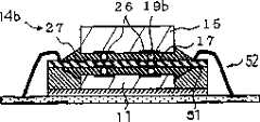
参阅图2,实现本发明的叠层封装半导体器件10包括半导体芯片组件14a,半导体倒装片15,层间连接件14b,球栅阵列14c,导线25和合成树脂外壳28。半导体芯片组件14a通过粘接剂层20粘着在球栅阵列14c上,信号和电源电压通过导电球23输送到半导体芯片组件14a中的半导体倒装片11上。电源电压和其它信号通过导电球23、导线25、密封外壳13上表面的导电图案24输送到半导体倒装片15上。在此实例中,导线25用金制成。半导体倒装片15翻转、使得导电焊盘26朝下。半导体倒装片11具有导电图案17,后者通过层间连接件14b电连接到半导体倒装片15的导电焊盘26。这样,半导体倒装片15通过层间连接件14b与半导体芯片11电连接,并通过层间连接件14b和导线25与球栅阵列14c电连接。半导体芯片组件14a、层间连接件14b、半导体倒装片15以及导线25都密封在合成树脂外壳28中。导电图案17包括多条相互电隔离的导电带,导电图案24也具有多条相互电隔离的导电带。Referring to FIG. 2, a stacked package semiconductor device 10 embodying the present invention includes a
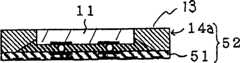
半导体芯片组件14a包括半导体倒装片11、底层填料树脂层12、合成树脂密封外壳13、导电图案17/18/24以及导电块19a。半导体倒装片11埋藏在密封外壳13中。不过,密封外壳13形成有凹进部分,并且设置在半导体倒装片11上表面的导电焊盘16暴露在凹进部分,如图所示。密封外壳13用半导体用途的环氧树脂制成,所述环氧树脂的玻璃转换温度为150℃。密封外壳13的机械强度应足够大,能使金属线接合时和金属线接合后导电图案24保持稳定。The
底层填料树脂层12充填在合成树脂外壳13中形成的凹部,导电图案17/18以及导电块19a内置于底层填料树脂层12中。导电图案17用作与半导体倒装片15的互连,导电图案18用于测试,即,用于对半导体倒装片11作诊断。导电图案17/18暴露于底层填料树脂层12的主表面之一,与半导体芯片组件14的上表面基本上共平面。导电块19a与导电图案17相接触,暴露于底层填料树脂层12的另一主表面。导电块19a与半导体倒装片11的导电焊盘16对准。这样,导电图案17通过导电块19a与导电焊盘16电连接,导电焊盘16又与半导体倒装片11中的集成电路电连接。底层填料树脂层12将导电块19a固定在导电焊盘16和导电图案17上,并防止半导体倒装片11受到污染和机械损坏。The
半导体芯片组件14a通过层间连接件14b与半导体芯片堆叠。层间连接件14b包括底层填料树脂层27和导电块19b。The
底层填料树脂层12上面叠加另一底层填料树脂层27,而埋在另一底层填料树脂层27中的导电块19b提供导电图案17和半导体倒装片15上的导电焊盘26之间的信号通路。导电焊盘26和半导体倒装片15的下表面用底层填料树脂层27覆盖。底层填料树脂层27紧密附着到底层填料树脂层12,并防止半导体倒装片15受到污染和机械损坏。Another
球栅阵列14c包括阻焊剂层21、导电布线图案22和导电球23。半导体芯片组件14a通过粘接剂层20附着在阻焊剂层21上表面的中心区域,导电图案22形成在阻焊剂层21上表面的周边区域。导电球23部分埋置在阻焊剂层21中并从阻焊剂层21的反向表面凸出。导电图案22包括多个导电带。The ball grid array 14 c includes a solder resist layer 21 , a
合成树脂外壳28由用于半导体用途的环氧树脂制成并且粘附在阻焊剂层21上。虽然半导体芯片组件14a、层间连接件14b、导电图案22、导线25和半导体倒装片15被密封在合成树脂外壳28中,但半导体倒装片15的反向表面却暴露在合成树脂外壳28的上表面。The
半导体倒装片11埋置在密封外壳13中,并且底层填料树脂层12加固了半导体倒装片11。这样,密封外壳13和底层填料树脂层12防止半导体倒装片11受到机械损坏,且半导体倒装片11在装配工作中不易破裂。因此,制造商可将半导体倒装片11作得非常薄。于是可制成轻而薄的叠层封装半导体器件10。The
同理,半导体倒装片15由合成树脂外壳支撑,并由底层填料树脂层27加固。半导体倒装片15不易破裂。因此,制造商可将半导体倒装片15作得尽可能的薄。Similarly, the
此外,底层填料树脂层12/27相互直接接触。换句话说,底层填料树脂层12附着到另一底层填料树脂层27,没有任何粘接剂层。半导体倒装片11和15之间的间隙窄到和导电块19a/19b及导电图案17一样。因此,层间连接件14b就比其两个表面上的印制薄膜5和粘接剂层的总厚度要薄。这样,叠层封装半导体器件10就比先有技术的叠层封装半导体器件要薄些,轻些。In addition, the underfill resin layers 12/27 are in direct contact with each other. In other words, the
以下参考图3A到3F和4A到4F说明根据本发明的叠层封装半导体器件10的制造工艺。The manufacturing process of the package-on-package semiconductor device 10 according to the present invention will be described below with reference to FIGS. 3A to 3F and 4A to 4F.
按照以下步骤制造半导体芯片组件14a。首先,制备铜衬底29。在铜衬底29的主表面上,用电镀技术在铜衬底29的主表面上淀积金层、镍层、铜层、镍层和金层,且将镍层和金层作成导电图案17/18/24,如图3A所示。金层为0.01微米到数微米厚,镍层为1微米到数微米厚,铜层为数微米到数十微米厚。The
然后,通过倒装片焊接技术将半导体倒装片62安装在导电图案17上。虽然图中未示出,但是铜衬底29上还有另一个半导体倒装片62,另一个半导体倒装片62也安装在它们的导电图案17上。在导电图案17和半导体倒装片62的导电焊盘16之间设置导电块19,如图3B所示。Then, the
然后,将合成树脂注入半导体倒装片62和铜衬底29之间的间隙。合成树脂充填半导体倒装片62和铜衬底29之间的间隙并扩散到半导体倒装片62四周。将合成树脂热固化、使得导电焊盘16、导电块19和导电图案17埋藏在底层填料树脂层12中,如图3C所示。Then, synthetic resin is injected into the gap between the
然后,将半导体倒装片62输送到铸模机(未示出)中,通过压铸技术将半导体倒装片62、导电图案17/18/24和底层填料树脂层12密封在合成树脂外壳中。将合成树脂热固化,如图3D所示。Then, the
然后,腐蚀掉铜衬底29、使得底层填料树脂层12中只留下导电图案17/18/24,如图3E所示。腐蚀完成之后,抛光合成树脂外壳13和半导体倒装片62、以便制成薄半导体芯片组件14a,如图3F所示。可以使用化学机械抛光技术来减小厚度。半导体芯片组件14a的厚度在10微米到150微米的范围内。半导体芯片组件14a与其他半导体芯片组件相分离。Then, the
这样,通过上述参考图3A到3F的过程就得到了半导体芯片组件14a。从减小叠层封装半导体器件10的厚度的观点来看,抛光步骤是可取的。半导体倒装片11已经用密封外壳13和底层填料层12a加固。半导体倒装片11能很好地耐受抛光过程中的机械力。Thus, the
通过图4A到4H所示的工艺序列来制造叠层封装半导体器件10。制造半导体芯片组件14a的过程可以部分与图4A到4H所示的过程相重叠。The package-on-package semiconductor device 10 is manufactured through the sequence of processes shown in FIGS. 4A to 4H . The process of manufacturing the
此过程以制备框架30开始。框架30用铜合金制成。用电镀技术将金、镍、铜、镍和金依次淀积在框架30的主表面上。金层、镍层、铜层、镍层和金层形成导电图案22,如图4A所示。金层为0.01微米到数微米厚,镍层为1微米到数微米厚,铜层为数微米到数十微米厚。The process begins with the preparation of
然后,用芯片焊接技术将半导体芯片组件14a安装到框架30上,用粘接剂浆或一片粘接剂箔把半导体芯片组件14a固定在导电图案22上。安装好以后,将粘接剂浆或所述粘接剂箔热固化。这样,半导体芯片组件14a就固定在框架30的导电图案22上,如图4B所示。虽然有多个半导体芯片组件14a安装在框架30上,在图4A到4H中仅示出一个半导体芯片组件14a,此处的说明也集中在所述半导体芯片组件14a上。Then, the
然后,用金属线接合技术将框架30上的导电图案22和密封外壳13上的导电图案24相连。导线25提供信号和电源的导电通路,如图4C所示。Then, the
然后,将半导体倒装片15的导电焊盘26与埋置在底层填料树脂层12中的导电图案17对准,并且用倒装片焊接技术将半导体倒装片15通过导电块19焊接到导电图案17上。将合成树脂注入半导体芯片组件14a和半导体倒装片15之间的间隙。合成树脂充填所述间隙并扩散到半导体倒装片15四周。将合成树脂热固化、使得半导体芯片组件14a与半导体倒装片15相重叠,如图4D所示。在另一种工艺序列中,在倒装片焊接之前注入合成树脂。底层填料塑料层12/27、导电块19a/19b以及导电图案17/18作为一个整体构成层间连接件14b。Then, the
然后将得到的结构送入压铸装置(未示出)中并密封在环氧树脂中。将环氧树脂热固化、使得半导体芯片组件14a,层间连接件14b和半导体倒装片15都被密封在合成树脂外壳28中,如图4E所示。The resulting structure was then fed into a die casting apparatus (not shown) and sealed in epoxy. The epoxy resin is thermally cured so that the
然后,用湿腐蚀技术去除掉框架30。在湿腐蚀中使用碱性腐蚀剂、使得铜成分被选择性地去除掉。于是,暴露出导电图案22,如图4F所示。Then, the
然后在所得所述反向表面形成阻焊剂层21。可以将可热固化树脂印制成图案。可热固化树脂可以均匀地扩散在所述反向表面,并且利用激光束在所述热固化树脂层中形成穿通孔。可以在粘接到所述反向表面之前在可热固化带中形成所述穿通孔。或者,穿通孔可以在热固化带粘接到所述反向表面之后形成。导电图案22部分地暴露在所述穿通孔之下,如图4G所示。A solder resist layer 21 is then formed on the resulting reverse surface. The heat curable resin can be printed into a pattern. A heat curable resin may be uniformly diffused on the reverse surface, and a through hole is formed in the heat curable resin layer using a laser beam. The through holes may be formed in the heat curable tape prior to bonding to the opposing surface. Alternatively, the through-holes may be formed after the heat-cured tape is bonded to the reverse surface. The
然后,将合成树脂外壳28局部抛光、使得半导体倒装片15暴露在合成树脂外壳28的上表面。在穿通孔设置焊料球并使之回熔、使得导电球23固定在导电图案22上,如图4H所示。可以用焊料膏代替所述焊球。用切片机将叠层封装半导体器件10与其他叠层封装半导体器件分开,这样就完成了叠层封装半导体器件10的制造。Then, the
在上述过程中,导电图案16,17,18,22和24是由金层,镍层,铜层,镍层,金层形成的。但是,其他组合也可以用于导电图案16/17/18/22/24。导电图案可以由金层,钯层,镍层,铜层,镍层,钯层,金层构成。也可从导电图案中把两层钯层删去一层。金层为0.01微米到数微米厚,钯层为0.01微米到数微米厚,镍层为1微米到数微米厚,而铜层为数微米到数十微米厚。In the above process, the
在上述过程中,使用焊料块作导电块19a/19b。在另一过程中,在层间连接件中可以使用小金块。阻焊剂层21可以用一片带有粘接剂的聚酰亚胺层而不是热固化合成树脂形成。In the above process, solder bumps are used as the
此外,金属线接合可以在半导体倒装片15和半导体芯片组件之间的倒装片焊接之后进行(见图4D)。合成数树脂外壳28的抛光,分割成叠层封装半导体器件以及导电球23的焊接步骤可以按照不同于上述顺序的其他顺序进行。In addition, wire bonding may be performed after flip chip bonding between the
从上述说明可知,合成数树脂外壳28和半导体芯片组件14a一样可以通过抛光减小其厚度。这是因为半导体倒装片15已经密封在合成数树脂外壳28中。换句话说,半导体倒装片15能很好耐受抛光过程中的机械力。这样,根据本发明的叠层封装半导体器件10又轻又薄,制造商使用本发明的叠层封装半导体器件10就可减小便携式电子产品的厚度和重量。第二实施例As can be seen from the above description, the
参阅图5,另一叠层封装半导体器件31也大致包括半导体芯片组件14a、层间连接件14b、半导体倒装片15、合成树脂外壳28和球栅阵列31a。组成部分14a,14b,15和28与第一实施例类似,只有球栅阵列31a与球栅阵列14c不同。故以下说明集中在球栅阵列14c上。Referring to FIG. 5 , another package-on-
球栅阵列31a包括绝缘衬底32、导电图案33/34和导电球23。每个导电图案33/34包括多个导电带。导电图案33的导电带选择性地与另一导电图案34的导电带相连接。刚性印制电路板、柔性印制薄膜,例如TAB(带式自动焊接)带或金属芯印制衬底都可用作绝缘衬底32。绝缘衬底32有两个主表面。半导体芯片组件14a通过粘接剂层20安装到一个主表面的中心区域上,而在所述主表面的四周区域形成导电图案34。导电图案34通过导线25连接到半导体芯片外壳28上。导电图案33形成在绝缘衬底32的另一主表面上,导电球23焊接到导电图案33上。虽然图5中未示出,但是,导电图案34通过层间连接图案连接到导电图案33,电信号和电源从导电球23输送到半导体倒装片11/15。The
与第一实施例类似,由于半导体芯片组件14a和合成树脂外壳的厚度减小,叠层封装半导体器件31又轻又薄。第三实施例Similar to the first embodiment, since the
图6示出实现本发明的又一叠层封装半导体器件35。在叠层封装半导体器件35中,半导体倒装片15由半导体芯片组件36代替。半导体芯片组件36的制造与半导体芯片组件14类似。半导体芯片组件14a与半导体芯片组件36重叠,层间连接件14b提供半导体芯片组件14a和36之间的信号通路。FIG. 6 shows yet another package-on-
半导体芯片组件36包括半导体倒装片15a、密封外壳13和底层填料树脂层12,并且导电块19b埋置在底层填料树脂层12中,用来将半导体倒装片11的集成电路电连接到半导体倒装片15a的集成电路上。由于两个半导体芯片组件14a/36都用密封外壳13和底层填料树脂层12加固,所以制造商可以减少半导体芯片组件14a/36的厚度而不会破坏半导体倒装片11/15a。这样,叠层封装半导体器件35的厚度就可减小,有助于按比例缩小便携式电子产品的尺寸。第四实施例The
图7示出实现本发明的另一叠层封装半导体器件37。与叠层封装半导体器件10不同之处在于半导体倒装片组件14a与多个半导体倒装片15b/15c重叠。半导体倒装片15b/15c并行设置在半导体芯片组件14a上,层间连接件14b提供半导体芯片组件14a的集成电路和多个半导体倒装片15b/15c的集成电路之间的信号通路。FIG. 7 shows another package-on-package semiconductor device 37 embodying the present invention. The difference from the package-on-package semiconductor device 10 is that the semiconductor
半导体芯片组件14a通过抛光减少厚度,密封外壳13和底层填料层12防止半导体倒装片11破裂。半导体倒装片15b/15c通过抛光也减少了厚度而不会破裂,因为半导体倒装片15b/15c已密封在合成树脂外壳28中。叠层封装半导体器件37有助于按比例缩小便携式电子产品的尺寸。第五实施例The
图8示出实现本发明的另一叠层封装半导体器件38。叠层封装半导体器件38与层封装半导体器件37不同之处在于半导体倒装片15b/15c由半导体芯片组件36a/36b代替。半导体芯片组件36a/36b的结构类似于半导体芯片组件36,为简明起见,在此不再详述。FIG. 8 shows another package-on-
半导体芯片组件14a/36a/36b通过抛光减少了厚度,使叠层封装半导体器件38又轻又薄。这样,叠层封装半导体器件38有助于按比例缩小便携式电子产品的尺寸。第六实施例The thickness of the
图9示出实现本发明的另一叠层封装半导体器件39。叠层封装半导体器件39与叠层封装半导体器件37不同之处在于半导体芯片组件14a由半导体芯片组件40代替。FIG. 9 shows another package-on-
半导体芯片组件40包括多个半导体倒装片11e/11f、多个底层填料层/导电图案/导电块12a/12b以及密封外壳13。半导体倒装片11e/11f并行设置在密封外壳13中,并在接外壳13中形成多个凹部。底层填料层/导电图案/导电块12a/12b分别充填所述凹部。在半导体芯片组件40和半导体倒装片15b/15c之间设置多个层间连接件14b,后者选择性地将半导体倒装片11e/11f的集成电路连接到半导体倒装片15b/15c的集成电路上。The
通过抛光减少半导体芯片组件40厚度、使得半导体倒装片11e/11f暴露于粘接剂层20。合成树脂外壳28也抛光,使半导体倒装片15b/15c暴露于合成树脂外壳28的外部。这样,叠层封装半导体器件39又轻又薄、使得制造商可以利用叠层封装半导体器件39按比例缩小便携式电子产品的尺寸。The thickness of the
半导体芯片组件40的制造工艺如下。首先,制备铜衬底29。在铜衬底29的主表面上构成导电图案17/24,如图10A所示。The manufacturing process of the
然后,通过倒装片焊接技术将半导体倒装片11e/11f安装在铜衬底29上,导电块19将半导体倒装片11e/11f上的导电焊盘16电连接到导电图案17上,如图10B所示。Then, the semiconductor flip chip 11e/11f is installed on the
然后,将合成树脂注入铜衬底29和半导体倒装片11e/11f之间的间隙,并扩散到半导体倒装片11e/11f四周。将合成树脂热固化、使得导电块19埋置在底层填料树脂层12中,如图10C所示。底层填料树脂层12固定了导电图案17和导电焊盘16之间的相对位置并加固了半导体倒装片11e/11f。Then, synthetic resin is injected into the gap between the
然后,将得到的结构放入模塑模具(未示出)中,将环氧树脂注入所述模塑模具。将环氧树脂热固化、使得半导体倒装片11e/11f、底层填料树脂层12和导电图案17/24密封在密封外壳13中,如图10D所示。The resulting structure was then placed into a molding mold (not shown) into which epoxy resin was injected. The epoxy resin is thermally cured so that the semiconductor flip chip 11e/11f, the
然后,腐蚀掉铜衬底29、以便暴露出导电图案17/24,如图10E所示。对密封外壳13和一部分半导体倒装片11e/11f进行抛光、使得半导体倒装片11e/11f暴露出来,如图10F所示。Then, the
最后,将半导体芯片组件40与同时密封在密封外壳中的其他半导体芯片组件分开。这样,半导体倒装片11e/11f就由密封外壳13和底层填料树脂层12加固。于是,半导体芯片组件40可通过抛光减少厚度而不会破裂。第七实施例Finally, the
图11示出实现本发明的另一叠层封装半导体器件50。叠层封装半导体器件50与叠层封装半导体器件10不同之处在于半导体芯片组件14a和插入层共同形成半导体芯片组件52,并且球栅阵列14c由球栅阵列31a代替。FIG. 11 shows another package-on-
导电图案17/18/24形成在插入层51的主表面上,用倒装片焊接技术将半导体芯片组件14a与插入层51装配在一起。刚性印刷电路板、柔性印制薄膜或导线框都可用作插入层51。在下主表面上的导电图案17与半导体倒装片11的导电焊盘16对准,埋置在底层填料树脂层12中的导电块19a连接在导电焊盘16和导电图案17之间。下主表面的导电图案17电连接到上主表面的导电图案17。导电焊盘26与上主表面的导电图案17对准,埋置在底层填料树脂层12中的导电块19b连接在导电图案和导电块26之间。这样,插入层51的导电图案17就将半导体芯片组件14a的导电块19a连接到层间连接件14b的导电块19b上。
底层填料树脂层12/27与插入层51的主表面保持接触、使得半导体芯片组件52与半导体倒装片15通过层间连接件14b重叠在一起。利用导线25将导电图案24连接到球栅阵列31a的导电图案34。球栅阵列31a的结构与叠层封装半导体器件31类似,为简明期起见,在此不作详述。The
半导体芯片组件50的制造工艺如下。首先,通过图12A到12E的工艺序列制造半导体芯片组件52。在绝缘衬底的主表面上形成导电图案17/18/24,并且获得插入层51,如图12A所示。导电焊盘16与导电图案17对准,利用导电块19将半导体倒装片62安装在插入层51上,如图12B所示。虽然插入层51上还有其他半导体倒装片62,但是图中仅示出一个半导体倒装片62。The manufacturing process of the
然后,将合成树脂注入插入层51和半导体倒装片62之间的间隙,并扩散到半导体倒装片62四周。将合成树脂热固化、使得底层填料树脂层12将半导体倒装片62固定在插入层51上,如图12C所示。将得到的结构放入模塑模具(未示出)中,将环氧树脂注入模塑模具。将环氧树脂热固化、使得半导体倒装片62和底层填料树脂层12密封在密封外壳13中,如图12D所示。Then, synthetic resin is injected into the gap between the
然后,将密封外壳13和部分半导体倒装片62抛光、使得其余的半导体倒装片11暴露在密封外壳13的外部,如图12E所示。最后,将所得的结构分开成半导体芯片组件52,图中示出半导体芯片组件52之一。Then, the sealing
通过图13A到13F的工艺序列将半导体芯片组件52和其他元件组装成叠层封装半导体器件50。过程开始时,先制备绝缘衬底32。在绝缘衬底32的主表面上形成导电图案33和34,如图13A所示。导电图案34与导电图案33电连接。虽然衬底32上同时装有多个半导体芯片组件52,但是,此处仅示出和说明一个半导体芯片组件52。The
然后将半导体芯片组件52翻转,安装在衬底52上,粘接剂层20夹在半导体芯片组件52和衬底32之间。将粘接剂层20热固化、使得半导体芯片组件52固定在衬底32上,如图13B所示。The
然后,用金属线接合技术把导线25焊接在导电图案24和导电图案34之间,如图13C所示。Then, the
然后,使半导体倒装片15的导电焊盘26与导电图案17对准,并利用导电块19与导电图案17电连接。这样,半导体芯片11上的集成电路通过插入层51和层间连接件14b电连接到半导体倒装片15上的集成电路。将合成树脂注入插入层51和半导体倒装片15之间的间隙,并扩散到半导体倒装片15四周。将合成树脂热固化、使得底层填料树脂层27将半导体倒装片15固定在插入层51上,如图13D所示。注入合成树脂和热固化可以先进行,然后在插入层51和半导体倒装片15之间进行倒装片焊接。Then, the
然后,将得到的结构放入压铸模具(未示出)中,将环氧树脂注入压铸模具。将环氧树脂热固化、使得半导体芯片组件52、半导体倒装片15和层间连接件14b被密封在合成树脂外壳28中,如图13E所示。Then, the resulting structure was placed into a die-casting mold (not shown), and epoxy resin was injected into the die-casting mold. The epoxy resin is thermally cured so that the
将合成树脂外壳28和半导体倒装片15抛光、使得半导体倒装片15暴露在外,如图13F所示。最后,将导电球23焊接到导电图案33上,将所得结构分割成叠层封装半导体器件50。The
金属线接合(见图13C)可以在倒装片安装后(见图13D)进行,抛光、分割以及导电球23的焊接步骤可以按不同的顺序进行。Wire bonding (see FIG. 13C ) can be performed after flip-chip mounting (see FIG. 13D ), and the steps of polishing, singulation, and soldering of
可以看出,半导体芯片组件52通过抛光可减小厚度(见图12E),叠层封装半导体器件50通过抛光可进一步减小厚度(见图13F)。半导体芯片组件52已经用密封外壳13和底层填料层12加固、使得半导体倒装片62能耐受抛光过程中的机械力。同理,半导体倒装片15已经用合成树脂外壳28加固、使得半导体倒装片15能耐受抛光过程中的机械力。第八实施例It can be seen that the thickness of the
图14示出实现本发明的另一叠层封装半导体器件53。叠层封装半导体器件53与叠层封装半导体器件50不同之处在于半导体倒装片15由半导体芯片组件54代替。虽然半导体倒装片15被包括在半导体芯片组件54之中,但半导体芯片组件54的其他特征与半导体芯片组件52类似,为简明起见,对半导体芯片组件54的说明在此省略。FIG. 14 shows another package-on-
将半导体芯片组件54翻转,用倒装片焊接技术将其连接到插入层51上。底层填料树脂层27将半导体芯片组件54固定到插入层51上,层间连接件14b将半导体倒装片11的集成电路电连接到半导体倒装片15的集成电路上。The
虽然半导体芯片组件54通过抛光其厚度减小,但密封外壳13和底层填料树脂层12/27加固了半导体倒装片11/15,防止半导体倒装片11/15在抛光过程中破裂。叠层封装半导体器件53又轻又薄,制造商利用叠层封装半导体器件53就可以按比例缩小便携式电子产品的尺寸。第九实施例Although the
图15示出实现本发明的另一叠层封装半导体器件55。叠层封装半导体器件55与叠层封装半导体器件50不同之处在于半导体芯片组件52与多个半导体倒装片15b/15c重叠。半导体倒装片15b/15c并行设置在半导体芯片组件52上,层间连接件14b将半导体芯片组件52的集成电路电连接到半导体倒装片15b/15c的集成电路上。FIG. 15 shows another package-on-package semiconductor device 55 embodying the present invention. The package-on-package semiconductor device 55 differs from the package-on-
虽然半导体芯片组件52和半导体倒装片15b/15c通过抛光其厚度减小,但密封外壳13、合成树脂外壳28和底层填料树脂层12/27加固了半导体倒装片11/15b/15c,防止半导体倒装片11/15b/15c在抛光过程中破裂。叠层封装半导体器件55又轻又薄,制造商利用叠层封装半导体器件55就可以按比例缩小便携式电子产品的尺寸。第十实施例Although the
图16示出实现本发明的另一叠层封装半导体器件56。叠层封装半导体器件56与叠层封装半导体器件55的不同之处在于半导体倒装片15b/15c由半导体芯片组件54a/54b代替。虽然半导体倒装片15被包括在半导体芯片组件54a/54b之中,但半导体芯片组件54a/54b的其他特征与半导体芯片组件52类似,为简明起见,对半导体芯片组件54a/54b的说明在此省略。FIG. 16 shows another package-on-package semiconductor device 56 embodying the present invention. The package-on-package semiconductor device 56 differs from the package-on-package semiconductor device 55 in that the
将半导体芯片组件54a/54b翻转,用倒装片焊接技术将其连接到插入层51上。底层填料树脂层27将半导体芯片组件54a/54b固定到插入层51上,层间连接件14b将半导体倒装片11的集成电路电连接到半导体倒装片15的集成电路上。The semiconductor chip assembly 54a/54b is turned over and connected to the
虽然半导体芯片组件52/54a/54b通过抛光其厚度减小,但密封外壳13和底层填料树脂层12/27加固了半导体倒装片11/15,防止半导体倒装片11/15在抛光过程中破裂。叠层封装半导体器件56又轻又薄,制造商利用叠层封装半导体器件53就可以按比例缩小便携式电子产品的尺寸。第十一实施例Although the thickness of the
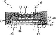
图17示出实现本发明的另一叠层封装半导体器件57。叠层封装半导体器件57与叠层封装半导体器件50的不同之处在于半导体芯片58插入在球栅阵列31和半导体芯片组件52之间。半导体芯片58的导电焊盘59通过导线25连接到导电图案34,并用粘接剂层20连接到衬底32上。FIG. 17 shows another package-on-
叠层封装半导体器件57具有叠层封装半导体器件50的全部优点。第十二实施例The package-on-
图18示出实现本发明的另一叠层封装半导体器件60。叠层封装半导体器件60与叠层封装半导体器件57的不同之处在于半导体芯片58是用倒装片焊接技术安装在衬底32上的。为此,在半导体芯片58的导电焊盘26和导电图案33之间设置有导电块19c,并且底层填料树脂层61将半导体芯片58固定在衬底32上。叠层封装半导体器件60具有叠层封装半导体器件50的全部优点。FIG. 18 shows another package-on-package semiconductor device 60 embodying the present invention. The package-on-package semiconductor device 60 differs from the package-on-
可以理解,插入层51被包括在半导体芯片组件52或组件52/54、52/54a/54b中并且被密封在密封外壳13或多个密封外壳13中、因此制造商可以通过抛光或研磨减少其厚度。半导体芯片组件52与其他半导体倒装片15或芯片15b/15c重叠并且所得结构被密封在合成树脂外壳28中。由于合成树脂外壳28的作用,半导体倒装片15或芯片15b/15c的厚度也可减少而不会使半导体倒装片破裂。It will be understood that the
层间连接件14b、插入层51和导线25可选择性地应用在叠层封装半导体器件10/31/35/37/38/39/50/53/55/56/57/60中,且将电信号和电源选择性地加到半导体倒装片的集成电路上。The
从前述说明可知,半导体倒装片已由密封外壳/合成树脂外壳以及底层填料层加固。虽然半导体倒装片经受抛光或研磨以减少厚度,但是外壳以及底层填料层防止了半导体倒装片的破裂。这样,制造商可减少半导体倒装片的厚度而不降低生产成品率。这样就制成了又轻又薄的叠层封装半导体器件。As can be seen from the foregoing description, a semiconductor flip chip has been reinforced by a hermetic case/synthetic resin case and an underfill layer. Although the semiconductor flip chip is subjected to polishing or grinding to reduce the thickness, the casing and underfill layers prevent the semiconductor flip chip from cracking. In this way, manufacturers can reduce the thickness of semiconductor flip chips without reducing production yield. Thus, a lightweight and thin stacked package semiconductor device is manufactured.
特别是,叠层封装半导体器件10,31,35,37,38和39具有通过倒装片焊接技术连接到半导体芯片组件36/36a/36b或倒装片15/15b/15c的半导体芯片组件14a/40。这就意味着对于其他半导体芯片组件和倒装片,不需要任何衬底。这产生非常薄的叠层封装半导体器件。半导体芯片组件14a/40/36/36a/36b的厚度在10微米到150微米范围内。即使半导体芯片组件14a/40与半导体芯片组件36/36a/36b重叠,总厚度也不超过400微米。这样,本发明的叠层封装半导体器件又轻又薄。In particular, the package-on-
导线25直接连接到在半导体芯片组件上直接形成的导电图案上。对于半导体芯片组件,不需要任何衬底。The
层间连接件14b允许制造商将半导体芯片组件14a/40与任何以不同的方式设计的半导体倒装片/半导体芯片组件重叠。这样,层间连接件14b提高了设计的灵活性。The
从生产成品率的观点来看,用于测试的导电图案18是需要的。制造商可以通过导电图案18测试半导体芯片组件或半导体组件。即使要把叠层封装半导体器件集成到多芯片组件中,半导体芯片组件/半导体组件在封装前均可单独进行诊断。这就提高了多芯片组件的生产成品率。From the standpoint of production yield, the
虽然以上示出并说明了本发明的特殊实施例,但是,对本专业的技术人员来说,显然可以进行各种变动和修改而不背离本发明的精神和范围。While particular embodiments of the present invention have been shown and described, it will be obvious to those skilled in the art that various changes and modifications can be made without departing from the spirit and scope of the invention.
层间连接件,即埋置在底层填料层的导电块,可用于组件之间以及组件和外部端子之间的连接。Interlayer connectors, which are conductive blocks embedded in the underfill layer, can be used for connections between components and between components and external terminals.
在上述实施例中,半导体芯片组件14a、半导体芯片组件40或半导体组件52对应于权利要求书中的一种半导体芯片组件,而半导体倒装片15、倒装片15b/15c、半导体芯片组件36、组件36a/36c、半导体芯片组件54或组件54a/54b用作半导体元件。导电块19b大体上构成埋藏在合成树脂片中的连接件。In the above embodiment, the
Claims (20)
Translated fromChineseApplications Claiming Priority (3)
| Application Number | Priority Date | Filing Date | Title |
|---|---|---|---|
| JP2002076114AJP2003273317A (en) | 2002-03-19 | 2002-03-19 | Semiconductor device and its manufacturing method |
| JP76114/2002 | 2002-03-19 | ||
| JP76114/02 | 2002-03-19 |
Publications (2)
| Publication Number | Publication Date |
|---|---|
| CN1445851Atrue CN1445851A (en) | 2003-10-01 |
| CN100364090C CN100364090C (en) | 2008-01-23 |
Family
ID=28035413
Family Applications (1)
| Application Number | Title | Priority Date | Filing Date |
|---|---|---|---|
| CNB031074804AExpired - Fee RelatedCN100364090C (en) | 2002-03-19 | 2003-03-19 | Thin stacked package semiconductor device and its manufacturing process |
Country Status (5)
| Country | Link |
|---|---|
| US (1) | US6762488B2 (en) |
| JP (1) | JP2003273317A (en) |
| KR (1) | KR100565930B1 (en) |
| CN (1) | CN100364090C (en) |
| TW (1) | TWI229425B (en) |
Cited By (6)
| Publication number | Priority date | Publication date | Assignee | Title |
|---|---|---|---|---|
| CN100477208C (en)* | 2003-12-24 | 2009-04-08 | 株式会社瑞萨科技 | Method for manufacturing semiconductor device |
| CN101243010B (en)* | 2005-08-11 | 2011-10-05 | 台湾积体电路制造股份有限公司 | Packaging of integrated circuit sensor and its manufacturing method |
| CN103117261A (en)* | 2011-11-16 | 2013-05-22 | 台湾积体电路制造股份有限公司 | Package structures and methods for forming the same |
| CN113540068A (en)* | 2021-07-20 | 2021-10-22 | 甬矽电子(宁波)股份有限公司 | Device stack packaging structure and device stack packaging method |
| CN113539861A (en)* | 2021-07-16 | 2021-10-22 | 芯知微(上海)电子科技有限公司 | Heterogeneous bare chip system integrated chip structure and manufacturing method thereof |
| WO2021248862A1 (en)* | 2020-06-09 | 2021-12-16 | 深圳市大疆创新科技有限公司 | Semiconductor packaging structure |
Families Citing this family (103)
| Publication number | Priority date | Publication date | Assignee | Title |
|---|---|---|---|---|
| US7053476B2 (en)* | 2002-09-17 | 2006-05-30 | Chippac, Inc. | Semiconductor multi-package module having package stacked over die-down flip chip ball grid array package and having wire bond interconnect between stacked packages |
| US7205647B2 (en)* | 2002-09-17 | 2007-04-17 | Chippac, Inc. | Semiconductor multi-package module having package stacked over ball grid array package and having wire bond interconnect between stacked packages |
| US20040061213A1 (en)* | 2002-09-17 | 2004-04-01 | Chippac, Inc. | Semiconductor multi-package module having package stacked over die-up flip chip ball grid array package and having wire bond interconnect between stacked packages |
| US7064426B2 (en) | 2002-09-17 | 2006-06-20 | Chippac, Inc. | Semiconductor multi-package module having wire bond interconnect between stacked packages |
| AU2003298595A1 (en)* | 2002-10-08 | 2004-05-04 | Chippac, Inc. | Semiconductor stacked multi-package module having inverted second package |
| US7034387B2 (en) | 2003-04-04 | 2006-04-25 | Chippac, Inc. | Semiconductor multipackage module including processor and memory package assemblies |
| US7122404B2 (en)* | 2003-03-11 | 2006-10-17 | Micron Technology, Inc. | Techniques for packaging a multiple device component |
| US6856009B2 (en)* | 2003-03-11 | 2005-02-15 | Micron Technology, Inc. | Techniques for packaging multiple device components |
| US6900502B2 (en)* | 2003-04-03 | 2005-05-31 | Taiwan Semiconductor Manufacturing Company, Ltd. | Strained channel on insulator device |
| TW200522293A (en)* | 2003-10-01 | 2005-07-01 | Koninkl Philips Electronics Nv | Electrical shielding in stacked dies by using conductive die attach adhesive |
| US8970049B2 (en) | 2003-12-17 | 2015-03-03 | Chippac, Inc. | Multiple chip package module having inverted package stacked over die |
| KR100575590B1 (en)* | 2003-12-17 | 2006-05-03 | 삼성전자주식회사 | Heat-Resistant Stacking Packages and Modules with They |
| US20060138631A1 (en)* | 2003-12-31 | 2006-06-29 | Advanced Semiconductor Engineering, Inc. | Multi-chip package structure |
| TWI283467B (en)* | 2003-12-31 | 2007-07-01 | Advanced Semiconductor Eng | Multi-chip package structure |
| JP2005209882A (en)* | 2004-01-22 | 2005-08-04 | Renesas Technology Corp | Semiconductor package and semiconductor device |
| JP4527991B2 (en)* | 2004-01-28 | 2010-08-18 | 株式会社日立製作所 | Multi-chip module manufacturing method |
| US7095105B2 (en)* | 2004-03-23 | 2006-08-22 | Texas Instruments Incorporated | Vertically stacked semiconductor device |
| JP4455158B2 (en)* | 2004-05-20 | 2010-04-21 | 株式会社ルネサステクノロジ | Semiconductor device |
| US20050269692A1 (en)* | 2004-05-24 | 2005-12-08 | Chippac, Inc | Stacked semiconductor package having adhesive/spacer structure and insulation |
| US8552551B2 (en) | 2004-05-24 | 2013-10-08 | Chippac, Inc. | Adhesive/spacer island structure for stacking over wire bonded die |
| US20050258527A1 (en) | 2004-05-24 | 2005-11-24 | Chippac, Inc. | Adhesive/spacer island structure for multiple die package |
| JP4561969B2 (en)* | 2004-05-26 | 2010-10-13 | セイコーエプソン株式会社 | Semiconductor device |
| JP4865197B2 (en) | 2004-06-30 | 2012-02-01 | ルネサスエレクトロニクス株式会社 | Semiconductor device and manufacturing method thereof |
| US7253511B2 (en)* | 2004-07-13 | 2007-08-07 | Chippac, Inc. | Semiconductor multipackage module including die and inverted land grid array package stacked over ball grid array package |
| TWI256091B (en)* | 2004-08-02 | 2006-06-01 | Siliconware Precision Industries Co Ltd | A semiconductor package having stacked chip package and a method |
| DE102004041888B4 (en)* | 2004-08-30 | 2007-03-08 | Infineon Technologies Ag | A manufacturing method of semiconductor device with stacked semiconductor devices |
| KR100639702B1 (en)* | 2004-11-26 | 2006-10-30 | 삼성전자주식회사 | Packaged semiconductor die and manufacturing method thereof |
| JP2006216911A (en)* | 2005-02-07 | 2006-08-17 | Renesas Technology Corp | Semiconductor device and encapsulated semiconductor package |
| US7160798B2 (en)* | 2005-02-24 | 2007-01-09 | Freescale Semiconductor, Inc. | Method of making reinforced semiconductor package |
| JP2008535273A (en)* | 2005-03-31 | 2008-08-28 | スタッツ・チップパック・リミテッド | Semiconductor stacked package assembly having substrate surfaces exposed on top and bottom surfaces |
| KR101213661B1 (en)* | 2005-03-31 | 2012-12-17 | 스태츠 칩팩, 엘티디. | Semiconductor assembly including chip scale package and second substrate and having exposed substrate surfaces on upper and lower sides |
| US7364945B2 (en) | 2005-03-31 | 2008-04-29 | Stats Chippac Ltd. | Method of mounting an integrated circuit package in an encapsulant cavity |
| US7589407B2 (en)* | 2005-04-11 | 2009-09-15 | Stats Chippac Ltd. | Semiconductor multipackage module including tape substrate land grid array package stacked over ball grid array package |
| US7547964B2 (en)* | 2005-04-25 | 2009-06-16 | International Rectifier Corporation | Device packages having a III-nitride based power semiconductor device |
| US7429786B2 (en)* | 2005-04-29 | 2008-09-30 | Stats Chippac Ltd. | Semiconductor package including second substrate and having exposed substrate surfaces on upper and lower sides |
| US7354800B2 (en)* | 2005-04-29 | 2008-04-08 | Stats Chippac Ltd. | Method of fabricating a stacked integrated circuit package system |
| US7582960B2 (en)* | 2005-05-05 | 2009-09-01 | Stats Chippac Ltd. | Multiple chip package module including die stacked over encapsulated package |
| US20060284298A1 (en)* | 2005-06-15 | 2006-12-21 | Jae Myun Kim | Chip stack package having same length bonding leads |
| US7394148B2 (en) | 2005-06-20 | 2008-07-01 | Stats Chippac Ltd. | Module having stacked chip scale semiconductor packages |
| US20070026573A1 (en)* | 2005-07-28 | 2007-02-01 | Aminuddin Ismail | Method of making a stacked die package |
| SG130055A1 (en)* | 2005-08-19 | 2007-03-20 | Micron Technology Inc | Microelectronic devices, stacked microelectronic devices, and methods for manufacturing microelectronic devices |
| SG130066A1 (en)* | 2005-08-26 | 2007-03-20 | Micron Technology Inc | Microelectronic device packages, stacked microelectronic device packages, and methods for manufacturing microelectronic devices |
| US7608523B2 (en)* | 2005-08-26 | 2009-10-27 | Disco Corporation | Wafer processing method and adhesive tape used in the wafer processing method |
| WO2007026392A1 (en) | 2005-08-30 | 2007-03-08 | Spansion Llc | Semiconductor device and method for manufacturing same |
| TWI324378B (en)* | 2005-10-21 | 2010-05-01 | Freescale Semiconductor Inc | Method of making semiconductor package with reduced moisture sensitivity |
| JP4744269B2 (en)* | 2005-11-02 | 2011-08-10 | パナソニック株式会社 | Semiconductor device and manufacturing method thereof |
| US20070152314A1 (en)* | 2005-12-30 | 2007-07-05 | Intel Corporation | Low stress stacked die packages |
| US7768125B2 (en) | 2006-01-04 | 2010-08-03 | Stats Chippac Ltd. | Multi-chip package system |
| US7456088B2 (en) | 2006-01-04 | 2008-11-25 | Stats Chippac Ltd. | Integrated circuit package system including stacked die |
| US7323774B2 (en)* | 2006-01-11 | 2008-01-29 | Stats Chippac Ltd. | Integrated circuit package system with pedestal structure |
| US20070164446A1 (en)* | 2006-01-13 | 2007-07-19 | Hawk Donald E Jr | Integrated circuit having second substrate to facilitate core power and ground distribution |
| US7750482B2 (en) | 2006-02-09 | 2010-07-06 | Stats Chippac Ltd. | Integrated circuit package system including zero fillet resin |
| US7435619B2 (en)* | 2006-02-14 | 2008-10-14 | Stats Chippac Ltd. | Method of fabricating a 3-D package stacking system |
| US8704349B2 (en) | 2006-02-14 | 2014-04-22 | Stats Chippac Ltd. | Integrated circuit package system with exposed interconnects |
| US8120156B2 (en)* | 2006-02-17 | 2012-02-21 | Stats Chippac Ltd. | Integrated circuit package system with die on base package |
| SG135066A1 (en) | 2006-02-20 | 2007-09-28 | Micron Technology Inc | Semiconductor device assemblies including face-to-face semiconductor dice, systems including such assemblies, and methods for fabricating such assemblies |
| DE102006016345A1 (en)* | 2006-04-05 | 2007-10-18 | Infineon Technologies Ag | Semiconductor module with discrete components and method for producing the same |
| US7384819B2 (en)* | 2006-04-28 | 2008-06-10 | Freescale Semiconductor, Inc. | Method of forming stackable package |
| US20070252260A1 (en)* | 2006-04-28 | 2007-11-01 | Micron Technology, Inc. | Stacked die packages |
| JP4791244B2 (en)* | 2006-05-11 | 2011-10-12 | 新光電気工業株式会社 | Electronic component built-in substrate and manufacturing method thereof |
| US20070281393A1 (en)* | 2006-05-30 | 2007-12-06 | Viswanadam Gautham | Method of forming a trace embedded package |
| JP2008091638A (en) | 2006-10-02 | 2008-04-17 | Nec Electronics Corp | Electronic equipment, and manufacturing method thereof |
| US7654079B2 (en)* | 2006-11-07 | 2010-02-02 | Cummins, Inc. | Diesel oxidation catalyst filter heating system |
| JP4965989B2 (en)* | 2006-12-19 | 2012-07-04 | 新光電気工業株式会社 | Electronic component built-in substrate and method for manufacturing electronic component built-in substrate |
| US7687897B2 (en)* | 2006-12-28 | 2010-03-30 | Stats Chippac Ltd. | Mountable integrated circuit package-in-package system with adhesive spacing structures |
| US9466545B1 (en)* | 2007-02-21 | 2016-10-11 | Amkor Technology, Inc. | Semiconductor package in package |
| US8134227B2 (en)* | 2007-03-30 | 2012-03-13 | Stats Chippac Ltd. | Stacked integrated circuit package system with conductive spacer |
| US8409920B2 (en)* | 2007-04-23 | 2013-04-02 | Stats Chippac Ltd. | Integrated circuit package system for package stacking and method of manufacture therefor |
| US8237259B2 (en)* | 2007-06-13 | 2012-08-07 | Infineon Technologies Ag | Embedded chip package |
| US8203214B2 (en)* | 2007-06-27 | 2012-06-19 | Stats Chippac Ltd. | Integrated circuit package in package system with adhesiveless package attach |
| US20110024890A1 (en)* | 2007-06-29 | 2011-02-03 | Stats Chippac, Ltd. | Stackable Package By Using Internal Stacking Modules |
| US7812435B2 (en)* | 2007-08-31 | 2010-10-12 | Stats Chippac Ltd. | Integrated circuit package-in-package system with side-by-side and offset stacking |
| US7872340B2 (en)* | 2007-08-31 | 2011-01-18 | Stats Chippac Ltd. | Integrated circuit package system employing an offset stacked configuration |
| US8378472B2 (en)* | 2007-10-17 | 2013-02-19 | Panasonic Corporation | Mounting structure for semiconductor element with underfill resin |
| JP5068133B2 (en)* | 2007-10-17 | 2012-11-07 | 新光電気工業株式会社 | Semiconductor chip laminated structure and semiconductor device |
| KR100920044B1 (en) | 2007-11-30 | 2009-10-07 | 주식회사 하이닉스반도체 | Semiconductor package |
| KR100891537B1 (en)* | 2007-12-13 | 2009-04-03 | 주식회사 하이닉스반도체 | Substrate for semiconductor package and semiconductor package having same |
| US8947883B2 (en) | 2007-12-27 | 2015-02-03 | Sandisk Technologies Inc. | Low profile wire bonded USB device |
| US7948095B2 (en)* | 2008-02-12 | 2011-05-24 | United Test And Assembly Center Ltd. | Semiconductor package and method of making the same |
| US8067828B2 (en)* | 2008-03-11 | 2011-11-29 | Stats Chippac Ltd. | System for solder ball inner stacking module connection |
| US20100019392A1 (en)* | 2008-07-25 | 2010-01-28 | Tan Gin Ghee | Stacked die package having reduced height and method of making same |
| US8058715B1 (en)* | 2009-01-09 | 2011-11-15 | Amkor Technology, Inc. | Package in package device for RF transceiver module |
| US8460972B2 (en)* | 2009-11-05 | 2013-06-11 | Freescale Semiconductor, Inc. | Method of forming semiconductor package |
| TWI401752B (en)* | 2009-12-31 | 2013-07-11 | Advanced Semiconductor Eng | Method for making a chip package |
| DE102010007605B4 (en)* | 2010-02-11 | 2015-04-16 | Epcos Ag | Miniaturized component with two chips and method for its production |
| US8754516B2 (en)* | 2010-08-26 | 2014-06-17 | Intel Corporation | Bumpless build-up layer package with pre-stacked microelectronic devices |
| JP5943544B2 (en)* | 2010-12-20 | 2016-07-05 | 株式会社ディスコ | Manufacturing method of laminated device and laminated device |
| KR101739945B1 (en)* | 2011-05-02 | 2017-06-09 | 삼성전자주식회사 | Semiconductor Package And Manufacturing The Same |
| US8872318B2 (en)* | 2011-08-24 | 2014-10-28 | Tessera, Inc. | Through interposer wire bond using low CTE interposer with coarse slot apertures |
| US9141157B2 (en)* | 2011-10-13 | 2015-09-22 | Texas Instruments Incorporated | Molded power supply system having a thermally insulated component |
| US9620430B2 (en) | 2012-01-23 | 2017-04-11 | Taiwan Semiconductor Manufacturing Company, Ltd. | Sawing underfill in packaging processes |
| KR20130105175A (en)* | 2012-03-16 | 2013-09-25 | 삼성전자주식회사 | Semiconductor package having protective layer and method of forming the same |
| US9385006B2 (en)* | 2012-06-21 | 2016-07-05 | STATS ChipPAC Pte. Ltd. | Semiconductor device and method of forming an embedded SOP fan-out package |
| JP5607692B2 (en)* | 2012-08-22 | 2014-10-15 | ルネサスエレクトロニクス株式会社 | Electronic equipment |
| JP2014049733A (en)* | 2012-09-04 | 2014-03-17 | Fujitsu Semiconductor Ltd | Semiconductor device and semiconductor device manufacturing method |
| US8993380B2 (en) | 2013-03-08 | 2015-03-31 | Taiwan Semiconductor Manufacturing Company, Ltd. | Structure and method for 3D IC package |
| KR20140148112A (en)* | 2013-06-21 | 2014-12-31 | 삼성전기주식회사 | Image sensor package and the method of manufacturing thereof |
| CN104766836B (en)* | 2015-04-15 | 2017-10-27 | 苏州聚达晟芯微电子有限公司 | Elastic shock-resistant semiconductor packaging structure |
| FR3053158B1 (en)* | 2016-06-22 | 2018-11-16 | 3D Plus | METHOD FOR COLLECTIVELY MANUFACTURING 3D CONFIGURED ELECTRONIC MODULES TO OPERATE AT MORE THAN 1 GHZ |
| JP2020043258A (en)* | 2018-09-12 | 2020-03-19 | キオクシア株式会社 | Semiconductor memory and manufacturing method thereof |
| US20200118991A1 (en)* | 2018-10-15 | 2020-04-16 | Intel Corporation | Pre-patterned fine-pitch bond pad interposer |
| JP7226358B2 (en)* | 2020-02-05 | 2023-02-21 | 株式会社デンソー | Electronics |
| US11373946B2 (en)* | 2020-03-26 | 2022-06-28 | Taiwan Semiconductor Manufacturing Company, Ltd. | Semiconductor package and manufacturing method thereof |
Family Cites Families (8)
| Publication number | Priority date | Publication date | Assignee | Title |
|---|---|---|---|---|
| JP2526511B2 (en)* | 1993-11-01 | 1996-08-21 | 日本電気株式会社 | Semiconductor device |
| KR0137826B1 (en)* | 1994-11-15 | 1998-04-28 | 문정환 | Package method and device package |
| TW373308B (en)* | 1995-02-24 | 1999-11-01 | Agere Systems Inc | Thin packaging of multi-chip modules with enhanced thermal/power management |
| JPH10256470A (en)* | 1997-03-10 | 1998-09-25 | Sanyo Electric Co Ltd | Semiconductor device |
| US5923090A (en)* | 1997-05-19 | 1999-07-13 | International Business Machines Corporation | Microelectronic package and fabrication thereof |
| JP3644662B2 (en)* | 1997-10-29 | 2005-05-11 | 株式会社ルネサステクノロジ | Semiconductor module |
| JP2001223326A (en)* | 2000-02-09 | 2001-08-17 | Hitachi Ltd | Semiconductor device |
| TWI237354B (en)* | 2002-01-31 | 2005-08-01 | Advanced Semiconductor Eng | Stacked package structure |
- 2002
- 2002-03-19JPJP2002076114Apatent/JP2003273317A/enactivePending
- 2003
- 2003-02-26TWTW092104008Apatent/TWI229425B/ennot_activeIP Right Cessation
- 2003-03-07USUS10/382,838patent/US6762488B2/ennot_activeExpired - Fee Related
- 2003-03-18KRKR1020030016796Apatent/KR100565930B1/ennot_activeExpired - Fee Related
- 2003-03-19CNCNB031074804Apatent/CN100364090C/ennot_activeExpired - Fee Related
Cited By (10)
| Publication number | Priority date | Publication date | Assignee | Title |
|---|---|---|---|---|
| CN100477208C (en)* | 2003-12-24 | 2009-04-08 | 株式会社瑞萨科技 | Method for manufacturing semiconductor device |
| CN101243010B (en)* | 2005-08-11 | 2011-10-05 | 台湾积体电路制造股份有限公司 | Packaging of integrated circuit sensor and its manufacturing method |
| CN103117261A (en)* | 2011-11-16 | 2013-05-22 | 台湾积体电路制造股份有限公司 | Package structures and methods for forming the same |
| US9679836B2 (en) | 2011-11-16 | 2017-06-13 | Taiwan Semiconductor Manufacturing Company, Ltd. | Package structures and methods for forming the same |
| US10510644B2 (en) | 2011-11-16 | 2019-12-17 | Taiwan Semiconductor Manufacturing Company, Ltd. | Package structures and methods for forming the same |
| US11342253B2 (en) | 2011-11-16 | 2022-05-24 | Taiwan Semiconductor Manufacturing Company, Ltd. | Package structures and methods for forming the same |
| US11961791B2 (en) | 2011-11-16 | 2024-04-16 | Taiwan Semiconductor Manufacturing Company, Ltd. | Package structures and methods for forming the same |
| WO2021248862A1 (en)* | 2020-06-09 | 2021-12-16 | 深圳市大疆创新科技有限公司 | Semiconductor packaging structure |
| CN113539861A (en)* | 2021-07-16 | 2021-10-22 | 芯知微(上海)电子科技有限公司 | Heterogeneous bare chip system integrated chip structure and manufacturing method thereof |
| CN113540068A (en)* | 2021-07-20 | 2021-10-22 | 甬矽电子(宁波)股份有限公司 | Device stack packaging structure and device stack packaging method |
Also Published As
| Publication number | Publication date |
|---|---|
| TWI229425B (en) | 2005-03-11 |
| KR20030076335A (en) | 2003-09-26 |
| US20030178716A1 (en) | 2003-09-25 |
| JP2003273317A (en) | 2003-09-26 |
| CN100364090C (en) | 2008-01-23 |
| US6762488B2 (en) | 2004-07-13 |
| TW200307354A (en) | 2003-12-01 |
| KR100565930B1 (en) | 2006-03-30 |
Similar Documents
| Publication | Publication Date | Title |
|---|---|---|
| CN1445851A (en) | Light-thin laminated packaged semiconductor device and manufacturing process thereof | |
| CN1207785C (en) | Semiconductor device, method of manufacturing electronic device, electronic device and portable information terminal | |
| CN1167122C (en) | Semiconductor device with a plurality of transistors | |
| US8786102B2 (en) | Semiconductor device and method of manufacturing the same | |
| US8294253B2 (en) | Semiconductor device, electronic device and method of manufacturing semiconductor device, having electronic component, sealing resin and multilayer wiring structure | |
| CN1551343A (en) | Electronic component packaging structure and manufacturing method thereof | |
| CN1956189A (en) | Stacked semiconductor device and lower layer module of stacked semiconductor device | |
| US10475752B2 (en) | Semiconductor package structure and method of making the same | |
| CN1779971A (en) | Semiconductor device and manufacturing method thereof | |
| CN1239589A (en) | Chip Scale Ball Grid Array for Integrated Circuit Packaging | |
| JP2004031607A (en) | Semiconductor device and manufacturing method thereof | |
| CN1815733A (en) | Semiconductor device and manufacturing method therefor | |
| CN1723556A (en) | Stackable semiconductor device and manufacturing method thereof | |
| CN1203454A (en) | Multi-chip module | |
| JP2010262992A (en) | Semiconductor module and portable apparatus | |
| JP2008218979A (en) | Electronic packaging and manufacturing method thereof | |
| CN1362733A (en) | Semiconductor device and manufacture method thereof, circuit board and electronic apparatus | |
| CN1787212A (en) | Multi-level semiconductor module and method for fabricating the same | |
| WO2007026392A1 (en) | Semiconductor device and method for manufacturing same | |
| JP4950743B2 (en) | Multilayer wiring board and manufacturing method thereof | |
| CN1402320A (en) | Circuit device mfg. method | |
| CN1702857A (en) | Semiconductor device and method for manufacturing the same | |
| CN1542963A (en) | Semiconductor device and manufacturing method thereof, electronic device, electronic instrument | |
| CN1830083A (en) | Semiconductor device and manufacturing method thereof | |
| JP4034468B2 (en) | Manufacturing method of semiconductor device |
Legal Events
| Date | Code | Title | Description |
|---|---|---|---|
| C06 | Publication | ||
| PB01 | Publication | ||
| C10 | Entry into substantive examination | ||
| SE01 | Entry into force of request for substantive examination | ||
| C14 | Grant of patent or utility model | ||
| GR01 | Patent grant | ||
| ASS | Succession or assignment of patent right | Owner name:RENESAS KANSAI CO., LTD. Free format text:FORMER OWNER: NEC CORP. Effective date:20100823 | |
| C41 | Transfer of patent application or patent right or utility model | ||
| COR | Change of bibliographic data | Free format text:CORRECT: ADDRESS; FROM: TOKYO, JAPAN TO: CHUANQI CITY, KANAGAWA, JAPAN COUNTY | |
| TR01 | Transfer of patent right | Effective date of registration:20100823 Address after:Kawasaki, Kanagawa, Japan Patentee after:Renesas Electronics Corporation Address before:Tokyo, Japan, Japan Patentee before:NEC Corp. | |
| C17 | Cessation of patent right | ||
| CF01 | Termination of patent right due to non-payment of annual fee | Granted publication date:20080123 Termination date:20140319 |