CN1445848A - Semiconductor device, manufacturing method thereof, and phase shift mask - Google Patents
Semiconductor device, manufacturing method thereof, and phase shift maskDownload PDFInfo
- Publication number
- CN1445848A CN1445848ACN03119849ACN03119849ACN1445848ACN 1445848 ACN1445848 ACN 1445848ACN 03119849 ACN03119849 ACN 03119849ACN 03119849 ACN03119849 ACN 03119849ACN 1445848 ACN1445848 ACN 1445848A
- Authority
- CN
- China
- Prior art keywords
- wall portion
- integrated circuit
- pattern
- semiconductor device
- film
- Prior art date
- Legal status (The legal status is an assumption and is not a legal conclusion. Google has not performed a legal analysis and makes no representation as to the accuracy of the status listed.)
- Granted
Links
Images


Classifications
- G—PHYSICS
- G03—PHOTOGRAPHY; CINEMATOGRAPHY; ANALOGOUS TECHNIQUES USING WAVES OTHER THAN OPTICAL WAVES; ELECTROGRAPHY; HOLOGRAPHY
- G03F—PHOTOMECHANICAL PRODUCTION OF TEXTURED OR PATTERNED SURFACES, e.g. FOR PRINTING, FOR PROCESSING OF SEMICONDUCTOR DEVICES; MATERIALS THEREFOR; ORIGINALS THEREFOR; APPARATUS SPECIALLY ADAPTED THEREFOR
- G03F1/00—Originals for photomechanical production of textured or patterned surfaces, e.g., masks, photo-masks, reticles; Mask blanks or pellicles therefor; Containers specially adapted therefor; Preparation thereof
- G03F1/26—Phase shift masks [PSM]; PSM blanks; Preparation thereof
- H—ELECTRICITY
- H01—ELECTRIC ELEMENTS
- H01L—SEMICONDUCTOR DEVICES NOT COVERED BY CLASS H10
- H01L23/00—Details of semiconductor or other solid state devices
- H01L23/562—Protection against mechanical damage
- H—ELECTRICITY
- H01—ELECTRIC ELEMENTS
- H01L—SEMICONDUCTOR DEVICES NOT COVERED BY CLASS H10
- H01L23/00—Details of semiconductor or other solid state devices
- H01L23/564—Details not otherwise provided for, e.g. protection against moisture
- H—ELECTRICITY
- H01—ELECTRIC ELEMENTS
- H01L—SEMICONDUCTOR DEVICES NOT COVERED BY CLASS H10
- H01L23/00—Details of semiconductor or other solid state devices
- H01L23/58—Structural electrical arrangements for semiconductor devices not otherwise provided for, e.g. in combination with batteries
- H01L23/585—Structural electrical arrangements for semiconductor devices not otherwise provided for, e.g. in combination with batteries comprising conductive layers or plates or strips or rods or rings
- G—PHYSICS
- G03—PHOTOGRAPHY; CINEMATOGRAPHY; ANALOGOUS TECHNIQUES USING WAVES OTHER THAN OPTICAL WAVES; ELECTROGRAPHY; HOLOGRAPHY
- G03F—PHOTOMECHANICAL PRODUCTION OF TEXTURED OR PATTERNED SURFACES, e.g. FOR PRINTING, FOR PROCESSING OF SEMICONDUCTOR DEVICES; MATERIALS THEREFOR; ORIGINALS THEREFOR; APPARATUS SPECIALLY ADAPTED THEREFOR
- G03F1/00—Originals for photomechanical production of textured or patterned surfaces, e.g., masks, photo-masks, reticles; Mask blanks or pellicles therefor; Containers specially adapted therefor; Preparation thereof
- G03F1/26—Phase shift masks [PSM]; PSM blanks; Preparation thereof
- G03F1/32—Attenuating PSM [att-PSM], e.g. halftone PSM or PSM having semi-transparent phase shift portion; Preparation thereof
- H—ELECTRICITY
- H01—ELECTRIC ELEMENTS
- H01L—SEMICONDUCTOR DEVICES NOT COVERED BY CLASS H10
- H01L21/00—Processes or apparatus adapted for the manufacture or treatment of semiconductor or solid state devices or of parts thereof
- H01L21/70—Manufacture or treatment of devices consisting of a plurality of solid state components formed in or on a common substrate or of parts thereof; Manufacture of integrated circuit devices or of parts thereof
- H01L21/71—Manufacture of specific parts of devices defined in group H01L21/70
- H01L21/768—Applying interconnections to be used for carrying current between separate components within a device comprising conductors and dielectrics
- H01L21/76801—Applying interconnections to be used for carrying current between separate components within a device comprising conductors and dielectrics characterised by the formation and the after-treatment of the dielectrics, e.g. smoothing
- H01L21/76802—Applying interconnections to be used for carrying current between separate components within a device comprising conductors and dielectrics characterised by the formation and the after-treatment of the dielectrics, e.g. smoothing by forming openings in dielectrics
- H01L21/76807—Applying interconnections to be used for carrying current between separate components within a device comprising conductors and dielectrics characterised by the formation and the after-treatment of the dielectrics, e.g. smoothing by forming openings in dielectrics for dual damascene structures
- H01L21/76811—Applying interconnections to be used for carrying current between separate components within a device comprising conductors and dielectrics characterised by the formation and the after-treatment of the dielectrics, e.g. smoothing by forming openings in dielectrics for dual damascene structures involving multiple stacked pre-patterned masks
- H—ELECTRICITY
- H01—ELECTRIC ELEMENTS
- H01L—SEMICONDUCTOR DEVICES NOT COVERED BY CLASS H10
- H01L21/00—Processes or apparatus adapted for the manufacture or treatment of semiconductor or solid state devices or of parts thereof
- H01L21/70—Manufacture or treatment of devices consisting of a plurality of solid state components formed in or on a common substrate or of parts thereof; Manufacture of integrated circuit devices or of parts thereof
- H01L21/71—Manufacture of specific parts of devices defined in group H01L21/70
- H01L21/768—Applying interconnections to be used for carrying current between separate components within a device comprising conductors and dielectrics
- H01L21/76801—Applying interconnections to be used for carrying current between separate components within a device comprising conductors and dielectrics characterised by the formation and the after-treatment of the dielectrics, e.g. smoothing
- H01L21/76802—Applying interconnections to be used for carrying current between separate components within a device comprising conductors and dielectrics characterised by the formation and the after-treatment of the dielectrics, e.g. smoothing by forming openings in dielectrics
- H01L21/76807—Applying interconnections to be used for carrying current between separate components within a device comprising conductors and dielectrics characterised by the formation and the after-treatment of the dielectrics, e.g. smoothing by forming openings in dielectrics for dual damascene structures
- H01L21/76813—Applying interconnections to be used for carrying current between separate components within a device comprising conductors and dielectrics characterised by the formation and the after-treatment of the dielectrics, e.g. smoothing by forming openings in dielectrics for dual damascene structures involving a partial via etch
- H—ELECTRICITY
- H01—ELECTRIC ELEMENTS
- H01L—SEMICONDUCTOR DEVICES NOT COVERED BY CLASS H10
- H01L2221/00—Processes or apparatus adapted for the manufacture or treatment of semiconductor or solid state devices or of parts thereof covered by H01L21/00
- H01L2221/10—Applying interconnections to be used for carrying current between separate components within a device
- H01L2221/1005—Formation and after-treatment of dielectrics
- H01L2221/101—Forming openings in dielectrics
- H01L2221/1015—Forming openings in dielectrics for dual damascene structures
- H01L2221/1036—Dual damascene with different via-level and trench-level dielectrics
- H—ELECTRICITY
- H01—ELECTRIC ELEMENTS
- H01L—SEMICONDUCTOR DEVICES NOT COVERED BY CLASS H10
- H01L2924/00—Indexing scheme for arrangements or methods for connecting or disconnecting semiconductor or solid-state bodies as covered by H01L24/00
- H01L2924/0001—Technical content checked by a classifier
- H01L2924/0002—Not covered by any one of groups H01L24/00, H01L24/00 and H01L2224/00
- H—ELECTRICITY
- H01—ELECTRIC ELEMENTS
- H01L—SEMICONDUCTOR DEVICES NOT COVERED BY CLASS H10
- H01L2924/00—Indexing scheme for arrangements or methods for connecting or disconnecting semiconductor or solid-state bodies as covered by H01L24/00
- H01L2924/01—Chemical elements
- H01L2924/01078—Platinum [Pt]
- H—ELECTRICITY
- H01—ELECTRIC ELEMENTS
- H01L—SEMICONDUCTOR DEVICES NOT COVERED BY CLASS H10
- H01L2924/00—Indexing scheme for arrangements or methods for connecting or disconnecting semiconductor or solid-state bodies as covered by H01L24/00
- H01L2924/30—Technical effects
- H01L2924/301—Electrical effects
- H01L2924/3025—Electromagnetic shielding
Landscapes
- Physics & Mathematics (AREA)
- General Physics & Mathematics (AREA)
- Engineering & Computer Science (AREA)
- Power Engineering (AREA)
- Computer Hardware Design (AREA)
- Microelectronics & Electronic Packaging (AREA)
- Condensed Matter Physics & Semiconductors (AREA)
- Manufacturing & Machinery (AREA)
- Internal Circuitry In Semiconductor Integrated Circuit Devices (AREA)
- Semiconductor Integrated Circuits (AREA)
- Preparing Plates And Mask In Photomechanical Process (AREA)
- Exposure And Positioning Against Photoresist Photosensitive Materials (AREA)
- Testing Or Measuring Of Semiconductors Or The Like (AREA)
- Formation Of Insulating Films (AREA)
- Lead Frames For Integrated Circuits (AREA)
Abstract
Description
Translated fromChinese技术领域technical field
本发明涉及一种提高在多层布线结构中的防潮性能的半导体器件及其制造方法,以及可用于制造该半导体器件的相移掩膜。The present invention relates to a semiconductor device with improved moisture-proof performance in a multilayer wiring structure, a manufacturing method thereof, and a phase shift mask which can be used to manufacture the semiconductor device.
背景技术Background technique
最近几年,随着大规模集成电路的发展,多层布线结构的设计规格倾向于减小尺寸。因此,通过形成用于金属布线材料的薄膜并且直接蚀刻该薄膜而形成的一些布线太细而不能够制造。因此,采用下述方法作为形成该布线的方法。也就是说,在形成层间绝缘膜之后,在该层间绝缘膜中形成沟槽图案或通孔图案,并且把布线材料镶嵌在该图案的开口区域,从而形成布线。这种形成布线的方法被称为镶嵌方法。In recent years, with the development of large-scale integrated circuits, the design specifications of multilayer wiring structures tend to be reduced in size. Therefore, some wirings formed by forming a thin film of a material for metal wiring and directly etching the thin film are too thin to be manufactured. Therefore, the following method is adopted as a method of forming this wiring. That is, after an interlayer insulating film is formed, a trench pattern or a via hole pattern is formed in the interlayer insulating film, and a wiring material is embedded in an opening area of the pattern, thereby forming a wiring. This method of forming wiring is called a damascene method.
当通过蚀刻而形成布线时,W、Al或Al合金通常被用作为布线材料。但是,当采用镶嵌方法时,通常使用Cu,因为它具有低电阻率和对电子迁移具有高抵抗力。When forming wiring by etching, W, Al, or Al alloy is generally used as a wiring material. However, when the damascene method is employed, Cu is generally used because of its low resistivity and high resistance to electromigration.
在制造该半导体器件中,例如晶体管、接头、布线、焊盘这样的元件被形成在一个半导体晶片上。在此之后,该半导体晶片被分为多个芯片,每个芯片使用陶瓷或塑料来封装。In manufacturing the semiconductor device, elements such as transistors, contacts, wires, pads are formed on a semiconductor wafer. After this, the semiconductor wafer is divided into chips, each of which is packaged using ceramic or plastic.
为了加速信号的传输速率,这对于布线的性能是重要的,减小布线之间的电容以及在不同层面中提供的布线之间的寄生电容是有效的。因此,最近开发的重点被置于降低存在于相同层面中提供的布线之间的绝缘膜的介电常数和存在于不同层面中的布线之间的层间绝缘膜的介电常数,以及降低布线本身的电阻。另外,为了降低介电常数,除了氧化硅膜之外,氟掺杂的氧化硅膜、无机绝缘膜、有机绝缘膜等等最近被用作为层间绝缘膜,以取代氧化硅膜。通常,当材料的原子或分子之间的距离变大时,由于薄膜密度的降低导致介电常数变小。In order to speed up the transmission rate of signals, which is important for the performance of wiring, it is effective to reduce the capacitance between wirings and the parasitic capacitance between wirings provided in different layers. Therefore, the focus of recent development has been placed on lowering the dielectric constant of an insulating film existing between wirings provided in the same layer and the dielectric constant of an interlayer insulating film existing between wirings provided in different layers, and reducing the dielectric constant of wirings provided in different layers. own resistance. In addition, in order to lower the dielectric constant, in addition to the silicon oxide film, a fluorine-doped silicon oxide film, an inorganic insulating film, an organic insulating film, or the like has recently been used as an interlayer insulating film instead of the silicon oxide film. Generally, when the distance between atoms or molecules of a material becomes larger, the dielectric constant becomes smaller due to a decrease in film density.
但是,具有低介电常数的上述层间绝缘膜的热膨胀系数基本上与例如基片这样的其它构成材料的热膨胀系数不同。由于热膨胀系数的差别,导致随后的热处理产生较大热应力。热应力被集中在该芯片的边角上而造成应力集中,并且可能在芯片的边角出现层面之间的剥离或裂纹,潮气容易进入该芯片。由于上述热膨胀系数的差别导致的应力集中在采用镶嵌方法的半导体器件中特别显著。其原因是,根据该镶嵌方法存在热膨胀系数具有显著差别的大量部分,由于层间绝缘膜形成在平整的布线层等等上,沟槽图案等等被形成在层间绝缘膜中,并且在此之后,布线材料被嵌入在该开口区域中。因此,采用镶嵌方法的常规半导体器件具有难以保证足够的防潮性能的缺点。However, the thermal expansion coefficient of the above-mentioned interlayer insulating film having a low dielectric constant is basically different from that of other constituent materials such as the substrate. Due to the difference in thermal expansion coefficient, the subsequent heat treatment produces greater thermal stress. Thermal stress is concentrated on the corners of the chip to cause stress concentration, and peeling or cracks between layers may occur at the corners of the chip, and moisture easily enters the chip. Stress concentration due to the above-mentioned difference in thermal expansion coefficient is particularly remarkable in semiconductor devices employing the damascene method. The reason for this is that, according to the damascene method, there are a large number of portions having a significant difference in coefficient of thermal expansion, since an interlayer insulating film is formed on a flat wiring layer, etc., trench patterns, etc. are formed in the interlayer insulating film, and here Afterwards, wiring material is embedded in the opening area. Therefore, conventional semiconductor devices employing the damascene method have a disadvantage that it is difficult to ensure sufficient moisture-proof performance.
发明内容Contents of the invention
本发明考虑到上述缺点而作出,其目的是提供一种半导体器件及其制造方法,其可以避免芯片面积增加和保证高防潮性,并且防止在外围边缘部分脱离,以及提供一种用于制造这种半导体器件的相移掩膜。The present invention has been made in consideration of the above-mentioned disadvantages, and its object is to provide a semiconductor device and a manufacturing method thereof, which can avoid an increase in chip area and ensure high moisture resistance, and prevent detachment at peripheral edge portions, and provide a method for manufacturing the same. A phase shift mask for semiconductor devices.
经过研究,本发明的发明人获得下文所述的本发明的各种形式。As a result of research, the inventors of the present invention have arrived at various forms of the present invention described below.
根据本发明的半导体器件包括形成有集成电路的一个集成电路部分、包括在该集成电路部分周围的金属膜的主壁面部分、包括有选择地形成在该集成电路部分和主壁面部分之间的金属膜的副壁面部分。该集成电路部分、主壁面部分和副壁面部分共用一个半导体基片,并且一个或两个或更多个层间绝缘膜形成在该半导体基片之上,其中有选择地形成开孔。构成该集成电路的一部分线路和被提供到每个主壁面部分和副壁面部分的一部分金属膜基本上被形成为相同的层面。A semiconductor device according to the present invention includes an integrated circuit portion formed with an integrated circuit, a main wall portion including a metal film around the integrated circuit portion, a metal film including a metal film selectively formed between the integrated circuit portion and the main wall portion. The subwall portion of the membrane. The integrated circuit portion, the main wall portion and the sub wall portion share a semiconductor substrate, and one or two or more interlayer insulating films are formed on the semiconductor substrate in which openings are selectively formed. A part of the wiring constituting the integrated circuit and a part of the metal film provided to each of the main wall portion and the sub wall portion are formed in substantially the same level.
根据本发明,由于副壁面部分被有选择地形成在主壁面部分和集成电路部分之间,一个壁面部分有选择地具有主壁面部分和副壁面部分的双重结构。因此,即使当由于采用镶嵌方法导致较大应力集中在半导体基片等等的一角上时,应力也被分散到副壁面部分上,通过把副壁面部分置于应力容易集中的位置处。从而,弹性结构形成在不会由于层面之间的剥离、破裂等等而导致应力释放的位置处。因此,随着出现破裂情况的减少,可以保持潮气的进入比例,并且保证较高的防潮性能。另外,由于一部分布线和一部分金属膜基本上被形成为相同的层面,因此可以与布线同时地形成该金属膜。因此,可以避免处理步骤增加。According to the present invention, since the sub wall portion is selectively formed between the main wall portion and the integrated circuit portion, one wall portion selectively has a double structure of the main wall portion and the sub wall portion. Therefore, even when a large stress concentrates on a corner of the semiconductor substrate or the like due to the damascene method, the stress is dispersed to the sub-wall portion by placing the sub-wall portion at a position where stress easily concentrates. Thus, an elastic structure is formed at a position where stress is not released due to peeling, cracking, etc. between layers. Therefore, as the occurrence of cracking is reduced, the ingress ratio of moisture can be maintained, and high moisture-proof performance can be ensured. In addition, since a part of the wiring and a part of the metal film are basically formed in the same layer, the metal film can be formed simultaneously with the wiring. Therefore, an increase in processing steps can be avoided.
根据本发明的一种制造半导体器件的方法是制造这样一种半导体器件的方法,该半导体器件具有形成集成电路的集成电路部分和包括在该集成电路部分周围的金属膜的主壁面部分。该方法包括如下步骤:与集成电路部分和主壁面部分的形成同时进行,有选择地在集成电路部分和主壁面部分形成包括金属膜的副壁面部分。A method of manufacturing a semiconductor device according to the present invention is a method of manufacturing a semiconductor device having an integrated circuit portion forming an integrated circuit and a main wall portion including a metal film around the integrated circuit portion. The method includes the step of selectively forming a secondary wall portion including a metal film on the integrated circuit portion and the main wall portion simultaneously with the formation of the integrated circuit portion and the main wall portion.
根据本发明的相移掩膜是包括形成在透明基片上的相移膜和形成在该透明基片的划线(scribe line)区域中的遮光膜的相移掩膜。由划线区域所包围的区域包括要形成集成电路部分的集成电路区域,以及要形成在集成电路部分的外围的外围边缘部分的外围边缘区域。遮光膜至少形成在一部分外围边缘区域和集成电路区域中。A phase shift mask according to the present invention is a phase shift mask including a phase shift film formed on a transparent substrate and a light shielding film formed in a scribe line region of the transparent substrate. The area surrounded by the scribe area includes an integrated circuit area where the integrated circuit portion is to be formed, and a peripheral edge area where the integrated circuit portion is to be formed in a peripheral edge portion. The light shielding film is formed at least in a part of the peripheral edge region and the integrated circuit region.
附图说明Description of drawings
图1为示出根据本发明第一实施例的半导体器件的结构的布局;1 is a layout showing the structure of a semiconductor device according to a first embodiment of the present invention;
图2为示出第一实施例的集成电路部分的结构的截面示图;2 is a cross-sectional view showing the structure of an integrated circuit portion of the first embodiment;
图3为示出沿着图1中的I-I线截取的截面的截面示图;FIG. 3 is a cross-sectional view showing a cross section taken along line I-I in FIG. 1;
图4为示出第一实施例的阻值测量部分的结构的布局;FIG. 4 is a layout showing the structure of the resistance measuring portion of the first embodiment;
图5为沿着图4中的II-II线截取的截面示图;Fig. 5 is a cross-sectional view taken along line II-II in Fig. 4;
图6为示出根据本发明第二实施例的半导体器件的壁面部分的结构的布局;6 is a layout showing the structure of a wall portion of a semiconductor device according to a second embodiment of the present invention;
图7为示出根据本发明第三实施例的半导体器件的壁面部分的结构的布局;7 is a layout showing the structure of a wall portion of a semiconductor device according to a third embodiment of the present invention;
图8为示出根据本发明第四实施例的半导体器件的壁面部分的结构的布局;8 is a layout showing the structure of a wall portion of a semiconductor device according to a fourth embodiment of the present invention;
图9为示出根据本发明第五实施例的半导体器件的壁面部分的结构的布局;9 is a layout showing the structure of a wall portion of a semiconductor device according to a fifth embodiment of the present invention;
图10为示出根据本发明第六实施例的半导体器件的壁面部分的结构的布局;10 is a layout showing the structure of a wall portion of a semiconductor device according to a sixth embodiment of the present invention;
图11为示出根据本发明第七实施例的半导体器件的壁面部分的结构的布局;11 is a layout showing the structure of a wall portion of a semiconductor device according to a seventh embodiment of the present invention;
图12为示出根据本发明第八实施例的半导体器件的壁面部分的结构的布局;12 is a layout showing the structure of a wall portion of a semiconductor device according to an eighth embodiment of the present invention;
图13为示出根据本发明第九实施例的半导体器件的壁面部分的结构的布局;13 is a layout showing the structure of a wall portion of a semiconductor device according to a ninth embodiment of the present invention;
图14为示出根据本发明第十实施例的半导体器件的壁面部分的结构的布局;14 is a layout showing the structure of a wall portion of a semiconductor device according to a tenth embodiment of the present invention;
图15为示出根据本发明第十一实施例的半导体器件的壁面部分的结构的布局;15 is a layout showing the structure of a wall portion of a semiconductor device according to an eleventh embodiment of the present invention;
图16为示出根据本发明第十二实施例的半导体器件的壁面部分的结构的布局;16 is a layout showing the structure of a wall portion of a semiconductor device according to a twelfth embodiment of the present invention;
图17为示出根据本发明第十三实施例的半导体器件的壁面部分的结构的布局;17 is a layout showing the structure of a wall portion of a semiconductor device according to a thirteenth embodiment of the present invention;
图18A至图18M为按照处理次序示出制造根据本发明第一实施例的半导体器件的方法的截面示图;18A to 18M are cross-sectional views illustrating a method of manufacturing the semiconductor device according to the first embodiment of the present invention in order of processing;
图19为示出在形成焊盘之后的晶片的平面示图;FIG. 19 is a plan view showing a wafer after pads are formed;
图20为示出放大由图19中的虚线所示的区域的布局;FIG. 20 is a layout showing enlargement of the area shown by the dotted line in FIG. 19;
图21为示出主壁面部分2和副壁面部分3的结构的一个例子的截面示图;以及FIG. 21 is a sectional view showing an example of the structure of the
图22为示出当对图16中所示的第十二实施例执行替换时的结构的布局;FIG. 22 is a layout showing a structure when a replacement is performed on the twelfth embodiment shown in FIG. 16;
图23A和23B为示出根据本发明第十四实施例的相移掩膜的平面示图和截面示图;23A and 23B are a plan view and a cross-sectional view showing a phase shift mask according to a fourteenth embodiment of the present invention;
图24A和24B为示出根据本发明第十四实施例的相移掩膜的放大示图;24A and 24B are enlarged views showing a phase shift mask according to a fourteenth embodiment of the present invention;
图25A至25C为示出根据本发明第十五实施例的相移掩膜的放大示图;25A to 25C are enlarged views showing a phase shift mask according to a fifteenth embodiment of the present invention;
图26A和26B为示出根据本发明第十五实施例的相移掩膜的放大示图;26A and 26B are enlarged views showing a phase shift mask according to a fifteenth embodiment of the present invention;
图27A和27B为示出根据本发明第十六实施例的相移掩膜的放大示图;27A and 27B are enlarged views showing a phase shift mask according to a sixteenth embodiment of the present invention;
图28A和28B为示出根据本发明第十七实施例的相移掩膜的放大示图;28A and 28B are enlarged views showing a phase shift mask according to a seventeenth embodiment of the present invention;
图29A和29B为示出根据本发明第十八实施例的相移掩膜的放大示图;29A and 29B are enlarged views illustrating a phase shift mask according to an eighteenth embodiment of the present invention;
图30A和30B为示出一种相移掩膜的平面示图和截面示图;30A and 30B are a plan view and a cross-sectional view showing a phase shift mask;
图31为示出一个旁瓣(No.1)的示意图;以及Figure 31 is a schematic diagram showing a side lobe (No.1); and
图32为示出一个旁瓣(No.2)的示意图。Fig. 32 is a schematic diagram showing a side lobe (No. 2).
具体实施方式Detailed ways
在下文中,将参照附图具体描述根据本发明的实施例的半导体器件及其制造方法。Hereinafter, a semiconductor device and a method of manufacturing the same according to an embodiment of the present invention will be described in detail with reference to the accompanying drawings.
-第一实施例--First embodiment-
首先,将描述本发明的第一实施例。图1为示出根据本发明第一实施例的半导体器件的结构的布局。图2为示出第一实施例的集成电路部分的结构的截面示图,以及图3为示出沿着图1中的I-I线截取的截面的截面示图。图4为示出第一实施例的阻值测量部分的结构的布局,以及图5为沿着图4中的II-II线截取的截面示图。First, a first embodiment of the present invention will be described. FIG. 1 is a layout showing the structure of a semiconductor device according to a first embodiment of the present invention. 2 is a sectional view showing the structure of an integrated circuit portion of the first embodiment, and FIG. 3 is a sectional view showing a section taken along line I-I in FIG. 1 . 4 is a layout showing the structure of a resistance measuring portion of the first embodiment, and FIG. 5 is a sectional view taken along line II-II in FIG. 4 .
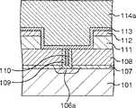
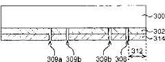
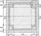
根据第一实施例,如图1中所示,提供例如矩形的主壁面部分2,以包围形成有半导体集成电路的集成电路部分1。根据本实施例的半导体器件被在主壁面部分2的外侧沿着主壁面部分2切割为小块,其在平面示图中为矩形。例如“L”形状的副壁面部分3被提供在主壁面部分2和集成电路部分1的每个角落之间。相互垂直的副壁面部分3的部分分别与相互垂直的主壁面部分2的部分相平行地延伸,即,对应于其侧边的部分。主壁面部分2和副壁面部分3之间的间距例如大约为1微米。另外,副壁面部分3的弯曲被置于最接近主壁面部分2的弯曲部分,即,对应于一个顶点的部分。另外,阻值测量部分(阻值测量装置)4被提供在副壁面部分3和集成电路部分1之间,用于测量该区域的阻值。在本实施例中,副壁面部分3为第一壁面块。According to the first embodiment, as shown in FIG. 1 , for example, a rectangular
在集成电路部分1中,如图2中所示形成多个MOS晶体管等等。例如,硅基片这样的半导体基片101被元件隔离绝缘膜102分为多个元件活性区。然后,栅绝缘膜103和栅极104被形成在半导体基片101上。在栅绝缘膜103和栅极104的侧面上,形成侧壁绝缘膜105。在半导体基片101的表面上,形成源/漏扩散层106,以在平面示图中把栅绝缘膜103和栅极104夹住。In the
另外,氮化硅膜107和氧化硅膜108例如形成在整个表面上,到达源/漏扩散层106的接触孔形成在氮化硅膜107和氧化硅膜108中。该接触孔的直径例如为大约0.10至0.20微米。另外,例如TiN膜106被形成为胶层,以覆盖接触孔的侧表面和底表面,每个接触孔中嵌有W膜110。In addition,
另外,例如有机绝缘膜111和氧化硅膜112形成在整个表面上,并且到达TiN膜109和W膜110的沟槽135形成在有机绝缘膜111和氧化硅膜112中。例如,Ta膜113被形成为阻挡金属膜,以覆盖沟槽135的侧表面和底表面,在每个沟槽中嵌有由Cu所制成的布线。In addition, for example, organic insulating
另外,氮化硅膜115和氧化硅膜116例如形成在整个表面上作为层间绝缘膜,并且到达作为布线114的下层布线的接触孔136形成在氮化硅膜115和氧化硅膜116中。该接触孔的直径例如约为0.15至0.25微米。In addition,
另外,有机绝缘膜117和氧化硅膜118例如形成在整个表面上,并且连接到形成于氮化硅膜115和氧化硅膜116中的接触孔136的沟槽137被形成在有机绝缘膜117和氧化硅膜118中。例如,Ta膜119被形成为阻挡金属膜,以覆盖接触孔136和沟槽137的侧表面和下表面,在该沟槽中嵌入有由Cu等所制成的布线120。In addition, the organic insulating
与上文所述相同,提供多个基本结构体121。每一个基本结构体由氮化硅膜115、氧化硅膜116、有机绝缘膜117、氧化硅膜118、Ta膜119和布线120所构成,在本实施例中总共有3个基本结构体121。As described above, a plurality of
另外,氮化硅膜122和氧化硅膜123被形成在最上方的基本结构体121上,并且到达构成最上方的基本结构体121的布线120的接触孔138被形成在氮化硅膜122和氧化硅膜123中。该接触孔例如具有大约1.00至1.10微米的直径。另外,形成阻挡金属膜124,以覆盖接触孔138的侧表面和底表面,并且覆盖氧化硅膜123的一部分表面,以及Al或Al合金膜(在下文中称为Al膜)125和阻挡金属膜126被形成在阻挡金属膜124上。另外,氧化硅膜127形成在整个表面上,以覆盖阻挡金属膜124、Al膜125和阻挡金属膜126,并且氮化硅膜128例如被形成在氧化硅膜127上,作为一个覆盖膜。In addition, a
顺便提及,当图2中所示的两个MOS晶体管构成一个CMOS晶体管时,在各个MOS晶体管之间扩散层106的导电类型各不相同,并且阱(未示出)被适当地形成在半导体基片101的表面中。Incidentally, when two MOS transistors shown in FIG. on the surface of the
同时,如图3中所示,扩散层106a被形成在主壁面部分2和副壁面部分3的半导体基片101的表面中。扩散层106a的导电类型没有特别地限制。另外,类似于集成电路部分1,例如氮化硅膜107和氧化硅膜108被形成在整个表面上,并且到达扩散层106a的沟槽被形成在氮化硅膜107和氧化硅膜108中。该沟槽例如具有大约0.15至0.30微米的厚度。TiN膜109例如被形成为胶层,以覆盖该沟槽的侧表面和底表面,每个沟槽中嵌有W膜110。Meanwhile, as shown in FIG. 3 , a
另外,类似于集成电路部分1,有机绝缘膜111和氧化硅膜112例如形成在整个表面上,并且到达TiN膜109和W膜110的沟槽被形成在有机绝缘膜111和氧化硅膜112中。该沟槽例如具有大约2微米的宽度。每个沟槽例如被形成为使得TiN膜109和W膜110被置于其中央。Ta膜113例如被形成为阻挡金属膜,以覆盖该沟槽的侧表面和底表面,在每个沟槽中嵌入有由Cu等所制成的金属膜114a。In addition, similarly to the
另外,类似于集成电路部分1,氮化硅膜115和氧化硅膜116例如形成在整个表面上,并且到达作为金属膜114a的下层金属膜的沟槽被形成在氮化硅膜115和氧化硅膜116中。该沟槽例如具有大约0.20至0.35微米的宽度。每个沟槽被形成为置于例如形成在有机绝缘膜111和氧化硅膜112中的沟槽的中央。因此,在平面示图中,该沟槽例如处于与形成在氮化硅膜107和氧化硅膜108中的沟槽相同的位置处。In addition, similarly to the
另外,类似于集成电路部分1,有机绝缘膜117和氧化硅膜118被形成在整个表面上,并且与形成于氮化硅膜115和氧化硅膜116中的沟槽相连接的沟槽被形成在有机绝缘膜117和氧化硅膜118中。该沟槽的宽度大约为2微米。该沟槽被形成为使得,形成在氮化硅膜115和氧化硅膜116中的沟槽被置于其中部。因此,在平面示图中,该沟槽例如处于与形成于有机绝缘膜111和氧化硅膜112中的沟槽相同的位置处。Ta膜119被形成为阻挡金属膜,以覆盖形成在氮化硅膜115和氧化硅膜116中的沟槽和形成在有机绝缘膜117和氧化硅膜118中的沟槽的侧表面和底表面上,在每个沟槽中嵌入有由Cu膜等等所制成的金属膜120a。In addition, similarly to the
类似于集成电路部分1,与上文所述相同,提供多个基本结构体121a。每一个基本结构体由氮化硅膜115、氧化硅膜116、有机绝缘膜117、氧化硅膜118、Ta膜119和布线120所构成,在本实施例中总共有3个基本结构体121a。Similar to the
另外,类似于集成电路部分1,氮化硅膜122和氧化硅膜123被形成在最上方的基本结构体121a上,并且到达构成最上方的基本结构体121a的金属膜120a的沟槽被形成在氮化硅膜122和氧化硅膜123中。该沟槽例如具有大约1.15至1.25微米的宽度。另外,形成阻挡金属膜124,以覆盖该沟槽的侧表面和底表面,并且覆盖氧化硅膜123的一部分表面,以及Al膜125和阻挡金属膜126被形成在阻挡金属膜124上。另外,氧化硅膜127形成在整个表面上,以覆盖阻挡金属膜124、Al膜125和阻挡金属膜126,并且氮化硅膜128例如被形成在氧化硅膜127上,作为一个覆盖膜。In addition, similarly to the
在副壁面部分3中,形成于氮化硅膜115和氧化硅膜116中的沟槽和形成于氮化硅膜122和氧化硅膜123中的窄沟槽131比形成于有机绝缘膜111和氧化硅膜112中的沟槽和形成于有机绝缘膜117和氧化硅膜118中的宽沟槽132更短,如图1中所示,窄沟槽131的两端被置于宽沟槽132的两端的内部。In the
如图1和图4中所示,两个梳状电极5a和5b被提供在阻值测量部分4中。梳状电极5a和5b的齿被以交替的方式设置。用于检查以保证防潮性的每个监控焊盘6a和6b连接到每个梳状电极5a和5b的一端。另外,在集成电路部分1和主壁面部分2之间不形成副壁面部分3和阻值测量部分4的区域中,在评估形成于集成电路部分1中的集成电路中,以适当的间隔提供用于从外部输入信号的多个评估焊盘7。As shown in FIGS. 1 and 4 , two
如图5中所示,梳状电极5a和5b的截面结构与主壁面部分2和副壁面部分3的截面结构相同,只是该金属膜不连接到该基片。但是,沟槽的宽度不同。也就是说,在梳状电极5a和5b中,形成于氮化硅膜115和氧化硅膜116中的沟槽以及形成于氮化硅膜122和氧化硅膜123中的窄沟槽133例如具有大约0.20至0.35微米的宽度,并且形成于有机绝缘膜111和氧化硅膜112中的沟槽以及形成于有机绝缘膜117和氧化硅膜118中的宽沟槽134例如具有大约0.6微米的宽度。另外,梳状电极5a和5b的齿之间的间距例如约为0.2微米。一部分Al膜125被从氮化硅膜128和氧化硅膜127暴露出来,以形成焊盘6a和6b。As shown in FIG. 5, the cross-sectional structure of the
在如此构成的第一实施例中,在平面示图中,“L”形状的副壁面部分3被有选择地提供在矩形的主壁面部分2的内部,并且在应力最集中的主壁面部分2的四个角处,构成主壁面部分2和副壁面部分3的多个金属膜被连接到半导体基片101,因此应力容易被分布在该角处。因此,与常规技术相比,即使由于热处理等等而导致应力集中,也不容易出现层面之间的剥离和裂缝。另外,由于主壁面部分2和副壁面部分3具有双重结构,因此即使在该角处出现裂缝,来自外部的潮气也不容易到达集成电路部分1。从而,根据本实施例,可以保证极高的防潮性。In the first embodiment thus constituted, in plan view, the "L"-shaped
另外,由于形成副壁面部分3的位置是不形成焊盘等等的区域,并且特别影响半导体器件的功能的元件不存在于现有技术中,因此即使当副壁面部分3被提供在该位置时,也不容易增加芯片面积。In addition, since the position where the
另外,主壁面部分2和副壁面部分3可以通过改变形成构成集成电路部分1的氮化硅膜、氧化硅膜、有机绝缘膜、布线等等的掩膜形状而形成,因此,还可以避免制造处理步骤的增加。In addition, the
另外,互不相同的电势可以被施加到阻值测量部分4中的焊盘6a和6b,从而测量它们之间的阻值。如果有潮气进来,则出现短路并且阻值减小。通过测量该阻值,可以确定是否有潮气进来。因此,可以获得高度可靠性。In addition, potentials different from each other can be applied to the
-第二实施例--Second embodiment-
接着,将描述本发明的第二实施例。图6为示出根据本发明第二实施例的半导体器件的壁面部分的结构的布局。Next, a second embodiment of the present invention will be described. 6 is a layout showing the structure of a wall portion of a semiconductor device according to a second embodiment of the present invention.
根据第二实施例,副壁面部分的结构与第一实施例不同。具体来说,如图6中所示,相对于弯折点,在副壁面部分3a中窄沟槽131的长度和宽沟槽132的长度为相同,并且各个末端部分在平面示图中处于相同的位置。除了上述沟槽的长度之外,与沟槽延伸方向垂直相交的副壁面部分3a的每个位置的截面的结构与第一实施例中的副壁面部分3相同。在本实施例中,副壁面部分3a是第一壁面块。According to the second embodiment, the structure of the sub wall portion is different from that of the first embodiment. Specifically, as shown in FIG. 6, the length of the
根据上述第二实施例,也可以获得与第一实施例相同的效果。According to the second embodiment described above, the same effects as those of the first embodiment can also be obtained.
-第三实施例--Third embodiment-
下面,将描述本发明的第三实施例。图7为示出根据本发明第三实施例的半导体器件的壁面部分的结构的布局。Next, a third embodiment of the present invention will be described. 7 is a layout showing the structure of a wall portion of a semiconductor device according to a third embodiment of the present invention.
根据第三实施例,副壁面部分的结构与第一实施例不同。具体来说,如图7中所示,副壁面部分3b具有一种平面形状,其中第一实施例的副壁面部分3的两个末端部分被垂直地弯向主壁面部分2侧,并且连接到主壁面部分2。另外,在副壁面部分3b中的窄沟槽131连接到主壁面部分2中的窄沟槽131,并且副壁面部分3b中的宽沟槽132连接到主壁面部分2中的宽沟槽132。除了上述平面形状之外,与沟槽延伸方向垂直相交的副壁面部分3b的每个位置的截面的结构与第一实施例中的副壁面部分3相同。在本实施例中,副壁面部分3b是第一壁面块。According to the third embodiment, the structure of the sub wall portion is different from that of the first embodiment. Specifically, as shown in FIG. 7, the sub wall portion 3b has a planar shape in which both end portions of the
根据上述第三实施例,也可以获得与第一实施例相同的效果。另外,由于副壁面部分连接到主壁面部分,因此裂缝不容易发展。从而,容易进入潮气的绝缘膜被完全在副壁面部分的内部和外部之间切断,从而不容易出现剥离。According to the third embodiment described above, the same effects as those of the first embodiment can also be obtained. In addition, since the sub wall portion is connected to the main wall portion, cracks are less likely to develop. Thereby, the insulating film, which easily enters moisture, is completely cut between the inside and the outside of the sub-wall surface portion, so that peeling does not easily occur.
-第四实施例--Fourth embodiment-
接着,将说明本发明的第四实施例。图8为示出根据本发明第四实施例的半导体器件的壁面部分的结构的布局。Next, a fourth embodiment of the present invention will be described. 8 is a layout showing the structure of a wall portion of a semiconductor device according to a fourth embodiment of the present invention.
根据第四实施例,副壁面部分的结构与第一实施例不同。具体来说,如图8中所示,副壁面部分3c的平面形状为矩形。除了上述平面形状之外,与沟槽延伸方向垂直相交的副壁面部分3c的每个位置的截面的结构与第一实施例中的副壁面部分3相同。另外,构成阻值测量部分4的梳状电极5a和5b(未在图8中示出)例如被设置为把副壁面部分3c夹在主壁面部分2与它们之间。更加具体来说,梳状电极5a和5b被沿着构成平面示图中矩形的副壁面部分3c的4边中远离主壁面部分2的顶点的两边而设置。在本例中,副壁面部分3c为四个壁面块。According to the fourth embodiment, the structure of the sub wall portion is different from that of the first embodiment. Specifically, as shown in FIG. 8, the planar shape of the
根据上述第四实施例,也可以获得与第一实施例相同的效果。According to the fourth embodiment described above, the same effects as those of the first embodiment can also be obtained.
-第五实施例--Fifth Embodiment-
接着,将描述本发明的第五实施例。图9为示出根据本发明第五实施例的半导体器件的壁面部分的结构的布局。Next, a fifth embodiment of the present invention will be described. 9 is a layout showing the structure of a wall portion of a semiconductor device according to a fifth embodiment of the present invention.
根据第五实施例,副壁面部分的结构不同于第一实施例。具体来说,如图9中所示,多个壁面块,在本实施例中为两个矩形壁面块3d1和3d2,被提供作为副壁面部分3d。在本实施例中,壁面块3d2是第四壁面块,并且壁面块3d1是第五壁面块。构成与向着沟槽的延伸方向垂直相交的副壁面部分3d的壁面块3d1和3d2的每个部分的截面结构与在第一实施例中的副壁面部分3相同,除了上述平面形状之外。According to the fifth embodiment, the structure of the sub wall portion is different from that of the first embodiment. Specifically, as shown in FIG. 9, a plurality of wall pieces, in this embodiment, two rectangular wall pieces 3d1 and 3d2, are provided as the
根据上述第五实施例,可以获得较高的防潮性。According to the fifth embodiment described above, high moisture resistance can be obtained.
顺便提及,副壁面部分3d可以由三个或多个壁面块所构成。Incidentally, the
-第六实施例--Sixth embodiment-
接着,将描述本发明的第六实施例。图10为示出根据本发明第六实施例的半导体器件的壁面部分的结构的布局。Next, a sixth embodiment of the present invention will be described. 10 is a layout showing the structure of a wall portion of a semiconductor device according to a sixth embodiment of the present invention.
根据第六实施例,副壁面部分的结构不同于第一实施例。具体来说,如图10中所示,例如三个壁面块3e1至3e3被设置为相对主壁面部分2的角在集成电路部分1的侧面上以等间距排列。每个壁面块3e1至3e3具有与第一实施例的副壁面部分3相同的结构。在本实施例中,壁面块3e1至3e3为第一壁面块。According to the sixth embodiment, the structure of the sub wall portion is different from that of the first embodiment. Specifically, as shown in FIG. 10 , for example, three wall pieces 3e1 to 3e3 are arranged at equal intervals on the side of the
根据上述第六实施例,类似于第五实施例,可以获得较高的防潮性。According to the sixth embodiment described above, similarly to the fifth embodiment, higher moisture resistance can be obtained.
顺便提及,副壁面部分3e可以由两个或四个或者更多个壁面块所构成,每个壁面块具有与副壁面部分3相同的结构。Incidentally, the sub-wall portion 3 e may be composed of two or four or more wall blocks each having the same structure as the
-第七实施例--Seventh embodiment-
接着,将描述本发明的第七实施例。图11为示出根据本发明第七实施例的半导体器件的壁面部分的结构的布局。Next, a seventh embodiment of the present invention will be described. 11 is a layout showing the structure of a wall portion of a semiconductor device according to a seventh embodiment of the present invention.
根据第七实施例,副壁面部分的结构与第一实施例不同。具体来说,如图11中所示,比壁面块3f2更短的壁面块3fl被设置在集成电路部分1上,在具有与第一实施例的副壁面部分3相同结构的壁面块3f2的旁边,以构成一个壁面块3f。与沟槽的延伸方向垂直相交的壁面块3fl的每个部分的截面结构与在第一实施例中的副壁面部分3相同。在本实施例中,壁面块3f2为第一壁面块,并且壁面块3fl为第一壁面块。According to the seventh embodiment, the structure of the sub wall portion is different from that of the first embodiment. Specifically, as shown in FIG. 11, a wall block 3f1 shorter than the wall block 3f2 is provided on the
根据上述第七实施例,类似于第五和第六实施例,也可以获得较高的防潮性。According to the seventh embodiment described above, similarly to the fifth and sixth embodiments, high moisture resistance can also be obtained.
-第八实施例--Eighth embodiment-
接着,将描述本发明的第八实施例。图12为示出根据本发明第八实施例的半导体器件的壁面部分的结构的布局。Next, an eighth embodiment of the present invention will be described. 12 is a layout showing the structure of a wall portion of a semiconductor device according to an eighth embodiment of the present invention.
根据第八实施例,副壁面部分的结构与第一实施例不同。具体来说,如图12中所示,围绕着第七实施例的壁面块3fl和3f2的壁面块3g1与主壁面部分2构成一个副壁面块3g。与沟槽的延伸方向垂直相交的壁面块3g1的每个部分的截面结构与在第一实施例中的副壁面部分3相同。在本实施例中,壁面块3g1为第三壁面块。According to the eighth embodiment, the structure of the sub wall portion is different from that of the first embodiment. Specifically, as shown in FIG. 12, a wall block 3g1 surrounding the wall blocks 3fl and 3f2 of the seventh embodiment and the
根据上述第8实施例,类似于第五至第七实施例,也可以获得较高的防潮性。According to the eighth embodiment described above, similarly to the fifth to seventh embodiments, higher moisture resistance can be obtained.
-第九实施例-- Ninth Embodiment -
接着,将描述本发明的第九实施例。图13为示出根据本发明第九实施例的半导体器件的壁面部分的结构的布局。Next, a ninth embodiment of the present invention will be described. 13 is a layout showing the structure of a wall portion of a semiconductor device according to a ninth embodiment of the present invention.
根据第九实施例,副壁面部分的结构与第一实施例不同。具体来说,如图13中所示,与第七实施例的壁面块3f1和3f2的沟槽132相同的宽沟槽132a被形成在壁面块3f1和3f2之间的有机绝缘膜117和氧化硅膜118中,并且Ta膜119和金属120a被嵌入沟槽132a中,以构成副壁面部分3h。According to the ninth embodiment, the structure of the sub wall portion is different from that of the first embodiment. Specifically, as shown in FIG. 13, the same
根据上述第9实施例,类似于第五至第八实施例,也可以获得较高的防潮性。According to the ninth embodiment described above, similarly to the fifth to eighth embodiments, higher moisture resistance can be obtained.
-第十实施例--Tenth embodiment-
接着,将描述本发明的第十实施例。图14为示出根据本发明第十实施例的半导体器件的壁面部分的结构的布局。Next, a tenth embodiment of the present invention will be described. 14 is a layout showing the structure of a wall portion of a semiconductor device according to a tenth embodiment of the present invention.
根据第十实施例,副壁面部分的结构与第一实施例不同。具体来说,如图14中所示,与第七实施例的壁面块3f1和3f2的沟槽132相同的宽沟槽132a被形成在壁面块3f1和3f2之间的有机绝缘膜117和氧化硅膜118中。另外,与壁面块3f1和3f2的沟槽132相同的窄沟槽131a被形成在壁面块3f1和3f2之间的氮化硅膜115和氧化硅膜118中。Ta膜119和金属120a被嵌入沟槽131a和132a中,以构成副壁面部分3i。According to the tenth embodiment, the structure of the sub wall portion is different from that of the first embodiment. Specifically, as shown in FIG. 14, the same
根据上述第10实施例,类似于第五至第九实施例,也可以获得较高的防潮性。According to the tenth embodiment described above, similarly to the fifth to ninth embodiments, higher moisture resistance can be obtained.
-第十一实施例--Eleventh embodiment-
接着,将描述本发明的第十一实施例。图15为示出根据本发明第十一实施例的半导体器件的壁面部分的结构的布局。Next, an eleventh embodiment of the present invention will be described. 15 is a layout showing the structure of a wall portion of a semiconductor device according to an eleventh embodiment of the present invention.
根据第十一实施例,副壁面部分的结构与第一实施例不同。具体来说,如图15中所示,提供“L”形状并且两端连接到主壁面部分2的副壁面部分3j。与沟槽的延伸方向垂直相交的壁面块3j的每个部分的截面结构与在第一实施例中的副壁面部分3相同。在本实施例中,壁面块3j为第六壁面块。According to the eleventh embodiment, the structure of the sub wall portion is different from that of the first embodiment. Specifically, as shown in FIG. 15 , a sub wall portion 3j having an “L” shape and having both ends connected to the
根据上述第十一实施例,类似于第五至第十实施例,也可以获得较高的防潮性。According to the eleventh embodiment described above, similarly to the fifth to tenth embodiments, high moisture resistance can also be obtained.
-第十二实施例-- Twelfth embodiment -
接着,将描述本发明的第十二实施例。图16为示出根据本发明第十二实施例的半导体器件的壁面部分的结构的布局。Next, a twelfth embodiment of the present invention will be described. 16 is a layout showing the structure of a wall portion of a semiconductor device according to a twelfth embodiment of the present invention.
根据第十二实施例,副壁面部分具有第一实施例的副壁面块3d和第十一实施例的副壁面块3j的组合而得的结构。具体来说,如图16中所示,第五实施例的壁面块3d1和3d2被置于与第十一实施例的副壁面部分3i相同结构的壁面部分3k1与主壁面部分2之间的方形区域中,以构成一个副面部分3k。在本实施例中,该壁面3k1为第六壁面块。According to the twelfth embodiment, the sub wall portion has a structure resulting from a combination of the
根据上述第12实施例,类似于第五至第十一实施例,也可以获得较高的防潮性。According to the above-mentioned twelfth embodiment, similarly to the fifth to eleventh embodiments, high moisture resistance can also be obtained.
-第十三实施例-- Thirteenth embodiment -
接着,将描述本发明的第十三实施例。图17为示出根据本发明第十三实施例的半导体器件的壁面部分的结构的布局。Next, a thirteenth embodiment of the present invention will be described. 17 is a layout showing the structure of a wall portion of a semiconductor device according to a thirteenth embodiment of the present invention.
根据第十三实施例,副壁面部分具有与第十二实施例不同的结构。具体来说,如图17中所示,宽沟槽132延伸到存在于构成第12实施例的副壁面部分3k的壁面块3d1和3d2之间的有机绝缘膜117和氧化硅膜118,并且进一步延伸到壁面部分3d2的方形区域内部。Ta膜119和金属膜120a被嵌于沟槽132中,以构成一个副壁面部分3m。According to the thirteenth embodiment, the sub wall portion has a different structure from that of the twelfth embodiment. Specifically, as shown in FIG. 17, the
根据上述第13实施例,类似于第五至第十二实施例,也可以获得较高的防潮性。According to the above-mentioned thirteenth embodiment, similarly to the fifth to twelfth embodiments, higher moisture resistance can be obtained.
-制造半导体器件的方法--Method of Manufacturing Semiconductor Device-
接着,将描述根据第一实施例的半导体器件的制造方法。图18A至图18M为按照处理次序示出制造根据本发明第一实施例的半导体器件的方法的截面示图。顺便提及,在图18A至图18M中示出对应于主壁面部分2的区域。Next, a method of manufacturing the semiconductor device according to the first embodiment will be described. 18A to 18M are cross-sectional views illustrating a method of manufacturing the semiconductor device according to the first embodiment of the present invention in process order. Incidentally, a region corresponding to the
首先,例如通过LOCOS方法、STI方法等等,在处于晶片的状态中的半导体基片101的表面上形成元件隔离绝缘膜102。然后,在集成电路部分1中形成栅绝缘膜103、栅极104、侧壁绝缘膜105和源/漏扩散层106。另外,在主壁面部分2和副壁面部分3中,与源/漏扩散层106的形成同时有选择地形成扩散成106a和106b。接着,例如通过等离子体CVD方法在整个表面上形成氮化硅膜107和氧化硅膜108。氮化硅膜107和氧化硅膜108例如分别具有70纳米和1000纳米的厚度。接着,例如通过化学机械抛光(CMP)方法平整氧化硅膜108,从而消除高度差。在平整处理之后,该氧化硅膜108的厚度例如为700纳米。然后,把光刻胶201施加到氧化硅膜108上,并且光刻胶201被曝光和显影。从而,用于在集成电路部分1中形成接触孔以及在主壁面部分2和副壁面部分3中形成窄沟槽131和133的图案201a形成在光刻胶201上。顺便提及,对于阻值测量部分4,与元件隔离绝缘膜102的形成同时,元件隔离绝缘膜可以形成在101的表面上,覆盖阻值测量部分4的整个表面。另外,在半导体基片101的表面上,元件隔离绝缘膜仅仅形成在要形成电极5a和5b的区域中。First, an element
然后,如图18B所示,通过使用光刻胶201作掩膜,使用CF气体对氧化硅膜108和氮化硅膜107进行各向异性蚀刻。从而在集成电路部分1中形成接触孔,并且窄沟槽131和133形成在主壁面部分2、副壁面部分3和阻值测量部分4中。然后,除去光刻胶201,并且例如通过溅射、CVD方法等等把TiN膜109被形成在接触孔、窄沟槽131和133以及氧化硅膜108中,作为胶层。另外,例如通过CVD方法等等在TiN膜109上形成W膜110。TiN膜109例如具有50纳米的厚度,并且W膜110例如具有400纳米的厚度。然后,CMP等等除去氧化硅膜108上的TiN膜109和W膜110,从而TiN膜109和W膜110仅仅被保留在接触孔和窄沟槽130和133中。Then, as shown in FIG. 18B, by using the photoresist 201 as a mask, the
下面描述在氧化硅膜108和氮化硅膜107的蚀刻过程中或者在光刻胶201的除去过程中对半导体基片101造成破坏的情况。首先,通过调节CF型气体的C含量与F含量的比值、C含量与H含量的比值、氧气或氩气的流量、总气压、分压比、温度、等离子体能量、基片电势等等这样的处理条件而适当地调节氧化硅膜108和氮化硅膜107的蚀刻选择比。然后,氧化硅膜108受到蚀刻。接着,通过使用氧气进行灰化而除去光刻胶201,然后,在不容易造成对半导体基片101的破坏的条件下对氮化硅膜107进行蚀刻。The following describes the case where damage is caused to the
在除去不必要的TiN膜109和W膜110之后,如图18C所示,例如通过在整个表面上进行旋涂而施加有机绝缘膜材料。然后,例如在400度的温度下对该有机绝缘膜材料进行60分钟的热处理。从而,该有机绝缘膜材料变硬,并且形成有机绝缘膜111。另外,在有机绝缘膜111上形成氧化硅膜112。有机绝缘膜111和氧化硅膜112例如具有250纳米的厚度。然后,把光刻胶202施加到氧化硅膜112上,并且该光刻胶被曝光和显影。从而,在光刻胶202中形成图案202a,用于在集成电路部分1中形成布线的沟槽135和在主壁面部分2、副壁面部分3和阻值测量部分4中形成宽沟槽132和134。After removing
从而,如图18D所示,通过使用光刻胶202作为掩膜对氧化硅膜112进行各向异性蚀刻,然后使用氢气和氮气的混合气体对有机绝缘膜111进行蚀刻。从而,在集成电路部分1中形成沟槽135,并且在主壁面部分2、副壁面部分3和阻值测量部分4中形成宽沟槽132和134。在此时,与有机绝缘膜111一同除去光刻胶202,但是在其下方的氧化硅膜112受到蚀刻。接着,例如通过溅射等方法在氧化硅膜112上形成Ta膜113作为阻挡金属膜。另外,例如通过电镀方法等等,在Ta膜113上形成用于成为布线114的布线材料和金属膜114a的薄膜,例如Cu膜。应当指出,当通过电镀方法形成用于布线材料的薄膜时,最好通过溅射方法在形成Ta膜113之后,形成一个种子层,以形成用布线材料的薄膜。Ta膜113例如具有30纳米的厚度,并且用于布线材料的薄膜例如具有1800纳米的厚度。Thus, as shown in FIG. 18D, the
从而,通过CMP方法等等除去Ta膜113和用于在氧化硅膜112上的布线材料的薄膜,从而,Ta膜113和用于布线材料的薄膜仅仅被保留在沟槽135、132和134中。结果,如图18E中所示,形成布线114和金属膜114a。Thus, the
然后,如图18F所示,氮化硅膜115和氧化硅膜116顺序地形成在整个表面上。氮化硅膜115例如具有50纳米的厚度,并且氧化硅膜116具有800纳米的厚度。氮化硅膜115作为一个阻蚀层和扩散防止层。然后,例如通过CMP方法平整该氧化硅膜116,从而消除高度差。在平整处理之后,氧化硅膜116例如具有400纳米的厚度。顺便提及,具有大约400纳米厚度的氧化硅膜116可以形成的氮化硅膜115上,以省略CMP处理。接着,有机绝缘膜117和氧化硅膜118顺序地形成在氧化硅膜116上。如上文所述,可以通过旋涂施加有机绝缘膜材料,使得该有机绝缘膜材料受到适当的热处理,并且使该有机绝缘膜材料硬化而形成有机绝缘膜117。有机绝缘膜117和氧化硅膜118例如具有250纳米的厚度。Then, as shown in FIG. 18F, a
在此之后,被用作为形成沟槽的硬膜的金属膜203形成在氧化硅膜118上。金属膜203例如为TiN膜,并且其厚度为100纳米。另外,光刻胶204被施加在金属膜203上,并且光刻胶204被曝光和显影。从而,用于在集成电路部分1中形成沟槽137和在主壁面部分2、副壁面部分3和阻值测量部分4中形成宽沟槽132和134的图案204a形成在光刻胶204中。After that, a
随后,如图18G中所示,通过使用光刻胶204作为掩膜,使用Cl型气体对金属膜203进行蚀刻。从而,图案204a转印到金属膜203上,以形成图案203a。然后,通过灰化除去光刻胶204。接着,光刻胶205被施加在整个表面上,并且光刻胶205被曝光和显影。从而,用于在集成电路部分1中形成接触孔136和用于在主壁面部分2、副壁面部分3和阻值测量部分4中形成窄沟槽131和133的图案205a被形成在光刻胶205上。Subsequently, as shown in FIG. 18G, by using the photoresist 204 as a mask, the
随后,如图18H所示,使用光刻胶205作为掩膜对氧化硅膜118进行蚀刻。另外,通过使用氧化硅膜118作为掩膜,使用氢气和氮气的混合气体对有机绝缘膜117进行蚀刻,从而在集成电路部分1中形成接触孔136以及在主壁面部分2、副壁面部分3和阻值测量部分4中形成窄沟槽131和133。在此时,与有机绝缘膜117一同除去光刻胶205,但是在其下方的金属膜203和氧化硅膜118不受到蚀刻。应当指出,如果在金属膜203上形成图案203a中没有造成偏移,则最好在蚀刻氧化硅膜118之前使用光刻胶205作为掩膜除去金属膜203不需要部分。Subsequently, as shown in FIG. 18H, the
随后,如图18I中所示,通过使用金属膜203和有机绝缘膜117作为掩膜对氧化硅膜118和116进行蚀刻。结果,图案203a被转印到氧化硅膜118上,并且在氧化硅膜118和有机绝缘膜117中形成的图案被转印到氧化硅膜116上。在此时,氧化硅膜118的蚀刻停止于有机绝缘膜117,并且氧化硅膜116的蚀刻停止于作为阻蚀层的氮化硅膜115上。Subsequently, as shown in FIG. 18I , the
随着,如图18J所示,使用金属膜203和氧化硅膜118作为掩膜对有机绝缘膜117进行各向异性蚀刻。然后,使用氧化硅膜118作为掩膜对氮化硅膜115进行各向异性蚀刻。结果,接触孔136和沟槽137被形成在集成电路部分1上,沟槽131和133形成在主壁面部分2和副壁面部分3上,并且沟槽132和134形成在阻值测量部分4上。顺便提及,在氮化硅膜115的各向异性蚀刻之后,可以执行有机绝缘膜117的各向异性蚀刻。Subsequently, as shown in FIG. 18J, the organic insulating
随后,如图18K所示,例如通过溅射方法把Ta膜119形成在沟槽131和135中,接触孔136中和金属膜203上作为阻挡金属膜。另外,通过电镀方法等等,把用于作为布线120的布线材料和金属膜120a的薄膜,例如Cu膜,形成在Ta膜119上。应当指出,当通过电镀方法形成用于布线材料的薄膜时,最好在通过溅射方法形成Ta膜119之后,形成一个种子层,然后,形成用于布线材料的薄膜。Ta膜119例如具有30纳米的厚度,并且用于布线材料的薄膜具有1800纳米的厚度。Subsequently, as shown in FIG. 18K, a
随后,通过CMP方法等等除去在氧化硅膜118上金属膜203、Ta膜119和用于布线材料的薄膜,从而Ta膜119和用于布线材料的薄膜仅仅保留在沟槽131至135中以及在接触孔136中。结果,如图18L所示,金属膜120a形成在主壁面部分2、副壁面部分3和阻值测量部分4中,并且布线120(未在图18L示出)形成在集成电路部分1中。接着,氮化硅膜115再次形成在整个表面上,并且图18F中所示的处理到图18L中所示的处理被重复预定的次数。Subsequently, the
然后,如图18M所示,在形成最上方的基本结构体121和121a之后,氮化硅膜122和氧化硅膜123形成在整个表面上。然后,使用形成有预定图案的光刻胶(未示出)把沟槽131和133以及接触孔138形成在氧化硅膜123和氮化硅膜122中。接着,在沟槽131和133、接触孔138中和氧化硅膜123上形成阻挡金属膜124和铝膜125,并且阻挡金属膜126形成在铝膜125上。接着,阻挡金属膜126、铝膜125和阻挡金属膜124被构图为预定形状,氧化硅膜127形成在形状的整个表面上。然后,氮化硅膜128形成在氧化硅膜127上,作为覆盖膜。Then, as shown in FIG. 18M, after forming the uppermost
随后,开口形成在氮化硅膜128和氧化硅膜127中的预定位置处,从而有选择地曝露阻挡金属膜126。另外,曝露的阻挡金属膜126受到蚀刻,从而曝露铝膜125。该被曝露部分变为用于检查以保证防潮性的监视焊盘6a和6b和评估焊盘7。图19为示出在形成焊盘之后的晶片的平面示图,以及图20为示出放大由图19中的虚线所示的区域的布局。当形成用于检查以保证防潮性的监视焊盘6a和6b和评估焊盘7时,存在与该晶片的外围相距固定距离或更远的有效芯片区域(由图19中的阴影区域所示)。然后,沿着作为相邻的主壁面部分2之间的中线的切割线9划分该有效芯片区域8,从而把该晶片分割为多个芯片。Subsequently, openings are formed at predetermined positions in the
因此,可以制造根据第一实施例的半导体器件。Therefore, the semiconductor device according to the first embodiment can be manufactured.
请注意,当制造第二至第十三实施例的半导体器件时,可以改变用于形成副壁面部分3和阻值测量部分4的图案。Note that the patterns for forming
-第十四实施例--Fourteenth embodiment-
在制造上述半导体器件的方法中,例如在光刻胶构图时使用一个相移掩膜,例如一个半色调型掩膜。In the method of manufacturing the above-mentioned semiconductor device, for example, a phase shift mask such as a halftone type mask is used in the resist patterning.
下面将使用图30A和30B说明该半色调相移掩膜。图30A和30B为示出该相移掩膜的平面示图和截面示图。图30A为平面示图,并且图30B为沿着图30A的III-III线截取的截面示图。The halftone phase shift mask will be described below using FIGS. 30A and 30B. 30A and 30B are a plan view and a cross-sectional view showing the phase shift mask. FIG. 30A is a plan view, and FIG. 30B is a cross-sectional view taken along line III-III of FIG. 30A .
如图30A和30B中所示,透明的相移掩膜402形成在透明基片400上。例如使用使透射光的相位偏移180度的相移掩膜作为相移掩膜402。As shown in FIGS. 30A and 30B , a transparent phase shift mask 402 is formed on a transparent substrate 400 . For example, a phase shift mask that shifts the phase of transmitted light by 180 degrees is used as the phase shift mask 402 .
在要形成集成电路部分的集成电路区域404中,相移掩膜402具有形成在其中的接触孔图案407。接触孔图案407用于形成接触孔。In an integrated circuit region 404 where part of the integrated circuit is to be formed, the phase shift mask 402 has a contact hole pattern 407 formed therein. The contact hole pattern 407 is used to form contact holes.
在要形成集成电路部分外围的外围边缘部分的外围边缘区域406中,相移掩膜402具有形成于其中的主壁面部分图案408和副壁面部分图案410。主壁面部分图案408为用于形成主壁面部分2的图案(参见图1)。副壁面部分图案410为用于形成副壁面部分3的图案(参见图1)。In a peripheral edge region 406 where a peripheral edge portion of the periphery of the integrated circuit portion is to be formed, the phase shift mask 402 has a main
在划线区域412中,一个遮光膜414形成在相移掩膜402上。请注意,划线区域412是当使用一个分档器顺序地进行转印和曝光时在晶片上相互重叠的相邻照射区域(多次曝光区域)。In the scribe area 412 , a light shielding film 414 is formed on the phase shift mask 402 . Note that the scribe area 412 is an adjacent shot area (multi-exposure area) overlapping each other on the wafer when transfer and exposure are sequentially performed using one stepper.
如此构成半色调相移掩膜。This constitutes a halftone phase shift mask.
半色调相移掩膜的使用导致通过相移掩膜402的光线与通过透射区域的光线之间具有180度的相位差,从而由于光的干涉可增加图案边缘附近的对比度。这样可以形成微小的集成电路部分。The use of the halftone phase shift mask results in a 180 degree phase difference between the light passing through the phase shift mask 402 and the light passing through the transmissive area, so that the contrast near the edge of the pattern can be increased due to light interference. This allows the formation of tiny integrated circuit sections.
但是,在常规的半色调相移掩膜中,当多个图案相邻时,有时在这些图案附近产生被称为旁瓣的不希望出现的异常图案。该问题是半色调相移掩膜所特有的。旁瓣是由于通过透明的相移掩膜所构成的图案的光线相互干涉所产生的。由于主壁面部分图案408和副壁面部分图案410被形成为直线,因此与接触孔图案407相比,曝光量较大。相应地,在主壁面部分和副壁面部分容易出现旁瓣。However, in conventional halftone phase shift masks, when a plurality of patterns are adjacent to each other, undesired abnormal patterns called side lobes sometimes occur near these patterns. This problem is specific to halftone phase shift masks. The side lobes are caused by the interference of light rays passing through the pattern formed by the transparent phase-shift mask. Since the main
下面将通过图31和图32说明当使用图30A和30B的半色调相移掩膜进行曝光时所产生的旁瓣。图31为示出一个旁瓣(No.1)的示意图。图32为示出一个旁瓣(No.2)的示意图。Next, side lobes generated when exposure is performed using the halftone phase shift mask of FIGS. 30A and 30B will be described with reference to FIGS. 31 and 32 . Fig. 31 is a schematic diagram showing one side lobe (No. 1). Fig. 32 is a schematic diagram showing a side lobe (No. 2).
如图31和图32的箭头所示,在具有L形图案的部分以及具有T形图案部分附近产生旁瓣。另外,有时还在具有直线形状图案中产生一个旁瓣,这未在图中示出。As shown by the arrows in FIGS. 31 and 32 , side lobes are generated near the portion with the L-shaped pattern and the portion with the T-shaped pattern. In addition, sometimes a side lobe is generated in a pattern having a straight line shape, which is not shown in the figure.
同时,日本专利公开No.8-279452公开一种通过形成伪开口区域而防止旁瓣的产生的技术。但是,当使用在该参考文件中描述的技术时,需要优化每次光刻的曝光条件等等,这需要大量的工作。另外,在该参考文献所述的技术中,难以避免在具有直线图案的部分中产生旁瓣。Meanwhile, Japanese Patent Laid-Open No. 8-279452 discloses a technique for preventing generation of side lobes by forming pseudo-opening regions. However, when the technique described in this reference is used, it is necessary to optimize exposure conditions and the like for each photolithography, which requires a lot of work. In addition, in the technique described in this reference, it is difficult to avoid generation of side lobes in portions having straight line patterns.
通过研究,本发明的发明人发现使用上述结构的相移掩膜可以制造上述半导体器件,并且防止出现旁瓣。Through research, the inventors of the present invention have found that the above-mentioned semiconductor device can be manufactured using the phase-shift mask of the above-mentioned structure, and the occurrence of side lobes can be prevented.
下面使用图23A、图23B、图24A和24B说明根据本发明的第十四实施例的相移掩膜。图23A和23B为示出根据本发明的相移掩膜平面示图和截面示图。图23A为平面示图,图23B为沿着图23A的III-III截取的截面示图。图24A和24B为示出根据本实施例的相移掩膜放大示图。图24A和24B示出图23A中的圆圈区域的放大示图。图24A为平面示图,图24B为沿着图24A的III-III截取的截面示图。尽管在图23A和23B中省略了一部分壁面部分块309b(参见图24A和24B),但是,在图23A和23B中省略的壁面部分块309b被在图24A和24B中示出。相同的参考标号和符号被用于表示与图1至图22中所示的第一至第十三实施例的半导体器件及其制造方法相同的构成部件,并且将省略或简化对它们的描述。A phase shift mask according to a fourteenth embodiment of the present invention will be described below using FIGS. 23A , 23B, 24A, and 24B. 23A and 23B are a plan view and a cross-sectional view showing a phase shift mask according to the present invention. FIG. 23A is a plan view, and FIG. 23B is a cross-sectional view taken along III-III of FIG. 23A . 24A and 24B are enlarged views showing a phase shift mask according to this embodiment. 24A and 24B show enlarged views of the circled area in FIG. 23A. FIG. 24A is a plan view, and FIG. 24B is a cross-sectional view taken along III-III of FIG. 24A . Although a part of the
下面将以对图18A中所示的光刻胶201进行构图所用的相移掩膜为例描述本实施例。具体来说,以一个相移掩膜为例来说明本实施例,该相移掩膜被用于在光刻胶201中形成图案201a等等,以形成到达源/漏扩散层106(参见图2)的接触孔以及到达扩散层106a(参见图3)的沟槽131(参见图1)。The present embodiment will be described below taking a phase shift mask used for patterning the photoresist 201 shown in FIG. 18A as an example. Specifically, the present embodiment will be described by taking a phase shift mask as an example, which is used to form a pattern 201a etc. 2) and the trench 131 (see FIG. 1 ) reaching the
在本实施例中,将以用于对图18A中所示的光刻胶201进行构图的相移掩膜为例进行说明,但是本发明的原理可以用于对例如光刻胶202(参见图18C)、光刻胶204(参见图18F)、光刻胶205(参见图18G)这样所有其它光刻胶进行构图。In this embodiment, the phase shift mask used for patterning the photoresist 201 shown in FIG. 18C), photoresist 204 (see FIG. 18F ), photoresist 205 (see FIG. 18G ) and all other photoresists for patterning.
如图23A和23B所示,一个相移膜302形成在透明基片300上。作为相移膜302的材料,例如可以使用光透射率约为4%至30%并且使光相位偏移180度的材料。更加具体来说,作为相移膜302的材料,例如可使用MoSi(硅化钼)等等。A
在要形成集成电路部分的集成电路区域304中,即在主区域中,相移膜302具有形成于其中的接触孔图案307。接触孔图案307为用于形成上述接触孔的图案。In the
在要形成集成电路部分外围的外围边缘部分的一个外围边缘区域306中,相移膜302具有形成于其中的主壁面部分图案308和副壁面部分图案310。主壁面部分图案308是用于形成上述主壁面部分2(参见图1)的图案。副壁面部分图案310是用于形成上述副壁面部分3(参见图1)的图案。In one
如图24A和图24B所示,副壁面部分图案310包括壁面部分块309a和壁面部分块309b。在外侧上的壁面部分块309a整体上为L形状。在内侧上形成多个壁面部分块309b。在内侧上的每个壁面部分块309b的形状近似为接触孔图案307的形状。多个壁面部分块309b整体上被排列为“方形”。顺便提及,整体上排列为方形的多个壁面部分块309b被排列为单个方形,但是整体上排列为方形的多个壁面部分块309b的结构不限于单个方形,并且可以是排列为二个方形或更多的方形。在外侧的壁面部分块309a连接到主壁面部分图案308,并且副壁面部分图案310的壁面部分块309a相互连接为T形图案。As shown in FIGS. 24A and 24B , the secondary
在划线区域312中,形成由Cr所构成的遮光膜314。In the
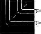
遮光膜314也形成在外围边缘区域306中。在本实施例中也在外围边缘区域306中形成遮光膜314的原因在下文中描述。遮光膜314防止光线通过相移膜302,从而可以减小在外围边缘区域306中出现光的干涉。这防止在外围边缘区域306中出现旁瓣。如图23A和23B所示,形成遮光膜314以覆盖从副壁面部分图案310的角向内延伸约1微米至5微米的范围。A
在外围边缘区域306中形成的图案尺寸比在集成电路区域304中形成的图案尺寸更大。在外围边缘区域306中形成的图案除了主壁面部分图案308和副壁面部分图案310之外还包括接触孔图案(未示出)等等。在下文中描述使外围边缘区域中的图案尺寸比集成电路区域的图案尺寸更大的理由。也就是说,在遮光膜314不覆盖的集成电路区域304的区域中,获得高分电率以形成微小的开口,另一方面,被遮光膜314所覆盖的相移膜302的区域具有低分辨率,从而难以形成微小的开口。结果,在作为图像平面的晶片上,主壁面部分2(参见图1)和副壁面部分3(参见图1)的宽度约为0.2微米至10微米,并且集成电路部分1的接触孔(未示出)的直径约为0.1微米至0.3微米。请注意,当减小比例为1/5时,作为图像平面的晶片上的尺寸变为比相移掩膜上的尺寸大5倍,并且当减小比例为1/4时,该尺寸比相移掩膜上的尺寸大四倍。The size of the pattern formed in the
如此构成根据本实施例的半色调相移掩膜。The halftone phase shift mask according to this embodiment is thus constituted.
根据本实施例的相移掩膜的主要特征在于遮光膜314也被形成在上述外围边缘区域306中。The main feature of the phase shift mask according to this embodiment is that the light-shielding
当使用图30A和30B中所示的相移掩膜时,光线通过相移膜302,在主壁面和副壁面部分的附近相互干涉,以在主壁面部分和副壁面部分附近产生旁瓣。When using the phase shift mask shown in FIGS. 30A and 30B , light rays passing through the
另一方面,在本实施例中,遮光膜314也形成在外围边缘区域306中,从而遮光膜314可以防止光通过外围边缘区域306中的相移膜302。因此,根据本实施例,可以减少在主壁面部分2和副壁面部分3附近的光线的相互干涉,以防止旁瓣的产生。On the other hand, in this embodiment, the
另外,由于在外围边缘区域306中形成的遮光膜314是与在划线区域312中形成的遮光膜314相同的薄膜,因此可以制造该相移掩膜而不增加制造的步骤数。In addition, since the
-第十五实施例-- Fifteenth embodiment -
下面将使用图25A至25C、图26A和26B说明根据本发明第十五实施例的相移掩膜。图25A至25C为示出根据本实施例的相移掩膜的平面示图和截面示图。图25A为平面示图,图25B为沿着图25A中的III-III线截取的截面示图,以及图25C为沿着图25A中的IV-IV线截取的截面示图。图26A和26B为示出根据本实施例的相移掩膜放大示图。图26A和26B示出图25A中的圆圈部分的放大示图。图26A为平面示图,以及图26B为沿着图26A的III-III线截取的截面示图。尽管在图25A和25C中省略一部分壁面部分块图案309b(参见图26A和26B),但是在图25A至25C中省略的壁面部分块图案309b在图26A和26B中示出。另外,尽管在图25A至图25C中省略一部分接触孔图案316(参见图26A和26B),但是在图25A至25C中省略的接触孔图案316在图26A和26B中示出。相同的参考标号和符号被用于表示与图1至图24B中所示的第一至第十四实施例相同的半导体器件、其制造方法以及相移掩膜,并且将省略和简化对它们的描述。A phase shift mask according to a fifteenth embodiment of the present invention will be described below using FIGS. 25A to 25C, FIGS. 26A and 26B. 25A to 25C are a plan view and a cross-sectional view showing a phase shift mask according to the present embodiment. 25A is a plan view, FIG. 25B is a sectional view taken along line III-III in FIG. 25A , and FIG. 25C is a sectional view taken along line IV-IV in FIG. 25A . 26A and 26B are enlarged diagrams showing a phase shift mask according to this embodiment. 26A and 26B show enlarged views of circled portions in FIG. 25A. FIG. 26A is a plan view, and FIG. 26B is a cross-sectional view taken along line III-III of FIG. 26A . Although a part of the wall
根据本实施例的相移掩膜的主要特征在于遮光膜314仅仅被有选择地形成在主壁面部分图案308和副壁面部分图案310附近。The main feature of the phase shift mask according to this embodiment is that the
如图25A至25C中所示,遮光膜314仅仅被有选择地形成在主壁面部分图案308和副壁面部分图案310附近的外围边缘区域306中。遮光膜314被形成为从主壁面部分图案308和副壁面部分图案310的边缘向内约1微米至约5微米的范围。As shown in FIGS. 25A to 25C , the
应当指出,形成遮光膜314的范围不限于从主壁面部分图案308和副壁面部分图案310的边缘向内1微米至5微米的范围。形成遮光膜314的范围可以被适当地设置为能够防止旁瓣产生的范围。It should be noted that the range of forming the light-shielding
除了主壁面部分图案308和副壁面部分图案310附近之外,遮光膜314不形成在外围边缘区域306的区域中。The
如图26A和图26B所示,接触孔图案316形成在没有形成遮光膜314的外围边缘区域306的区域中。接触孔图案316被构图,被用于形成到达MOS的源/漏扩散成的接触孔(未示出)。As shown in FIGS. 26A and 26B , a
类似于上文所述,遮光膜314形成在划线区域312中。Similar to the above, a
根据本实施例的相移掩膜的主要特征在于遮光膜314仅仅形成在主壁面部分图案308和副壁面部分图案310附近的相移膜302上。The main feature of the phase shift mask according to this embodiment is that the
在根据第十四实施例的相移掩膜中,遮光膜314形成在整个外围边缘区域306上。由于在形成遮光膜314的区域中的分辨率较低,因此当使用第十四实施例的相移掩膜时,不能够在外围边缘部分内形成微小的接触孔。相应地,当使用根据第十四实施例的相移掩膜时,不能够形成微小的MOS晶体管。In the phase shift mask according to the fourteenth embodiment, the
在另一方面,在本实施例中,遮光膜314仅仅被形成在外围区域中的主壁面部分图案308和副壁面部分图案310的附近。因此,根据本实施例,可以在不形成遮光膜314的外围边缘区域306中获得高分辨率。从而,根据本实施例,还可在外围边缘部分中形成微小的接触孔。因此,根据本实施例,还可以在外围边缘部分形成例如MOS晶体管这样的微小元件。根据本实施例,可以保证用于形成例如MOS晶体管这样的微小元件的宽区域,这可有助于减小芯片尺寸。On the other hand, in the present embodiment, the
-第十六实施例--Sixteenth embodiment-
下面将使用图27A和27B说明根据本发明第十六实施例的相移掩膜。图27A和27B示出根据本实施例的相移掩膜平面示图和截面示图。相同的参考标号和符号被用于表示与图1至图26B中所示的第一至第十五实施例相同的半导体器件、其制造方法以及相移掩膜,并且将省略和简化对它们的描述。A phase shift mask according to a sixteenth embodiment of the present invention will be described below using FIGS. 27A and 27B. 27A and 27B show a plan view and a cross-sectional view of a phase shift mask according to this embodiment. The same reference numerals and symbols are used to denote the same semiconductor devices, their manufacturing methods, and phase shift masks as those of the first to fifteenth embodiments shown in FIGS. 1 to 26B , and descriptions thereof will be omitted and simplified. describe.
根据本实施例的相移掩膜的主要特征在于遮光膜314不形成在外围边缘区域306中,使得主壁面部分图案308a和副壁面部分图案310a不具有直角而具有钝角,并且主壁面部分图案308a和副壁面部分图案310a被形成为相互隔离。The main feature of the phase shift mask according to this embodiment is that the
如图27A和27B中所示,在本实施例中,遮光膜314不被形成在外围边缘区域306中。As shown in FIGS. 27A and 27B , in the present embodiment, the
主壁面部分图案308a的边角部分不是直角而是钝角。具体来说,主壁面部分图案308a的边角部分的夹角为135度。The corner portions of the main
副壁面部分图案310a由壁面部分块图案309c和壁面部分块图案309b所构成。壁面部分块图案309c的边角部分不是直角而是钝角。具体来说,壁面部分图案309c的边角部分的夹角为135度。The sub-wall
在本实施例中,主壁面部分图案308a和副壁面部分图案310a不具有直角而具有钝角的原因是要消除具有L形图案的部分,以防止旁瓣的产生。In this embodiment, the main
应当指出,尽管在此把主壁面部分图案308a和副壁面部分图案310a的边角部分的夹角设置为135度,但是它不限于135度。当边角部分的夹角变钝时,可以在一定程度上减小旁瓣的产生。具体来说,当该边角部分的夹角为100度或更大时,可以有效地减小旁瓣的产生。当边角部分的夹角为110度或更大时,可以更加有效地减少旁瓣的产生。另外,当边角部分的夹角为120度或更大时,可以进一步减少旁瓣的产生。It should be noted that although the angle between the corner portions of the main
主壁面部分图案308a和副壁面部分图案310a被形成为相互分离。The main
在本实施例中,主壁面部分图案308a和副壁面部分图案310a相互分离的原因是要消除具有T形图案的部分,以防止旁瓣的产生。In this embodiment, the reason why the main
从而,根据本实施例,由于主壁面部分图案308a和副壁面部分图案310a的边角部分不是直角而是钝角,另外主壁面部分图案308a和副壁面部分图案310a被形成为相互分离,因此即使当遮光膜314不形成在主壁面部分图案308a和副壁面部分图案310a附近时,也可以防止在主壁面部分2和副壁面部分3附近产生旁瓣。Thus, according to the present embodiment, since the corner portions of the main
-第十七实施例-- Seventeenth embodiment -
下面将使用图28A和28B说明根据本发明第十七实施例的相移掩膜。图28A和28B示出根据本实施例的相移掩膜平面示图和截面示图。图28A为平面示图,以及图28B为沿着图28A的III-III线截取的截面。相同的参考标号和符号被用于表示与图1至图27B中所示的第一至第十六实施例相同的半导体器件、其制造方法以及相移掩膜,并且将省略和简化对它们的描述。A phase shift mask according to a seventeenth embodiment of the present invention will be described below using FIGS. 28A and 28B. 28A and 28B show a plan view and a cross-sectional view of a phase shift mask according to this embodiment. FIG. 28A is a plan view, and FIG. 28B is a cross section taken along line III-III of FIG. 28A . The same reference numerals and symbols are used to denote the same semiconductor devices, their manufacturing methods, and phase shift masks as those of the first to sixteenth embodiments shown in FIGS. 1 to 27B , and descriptions thereof will be omitted and simplified. describe.
根据本实施例的相移掩膜的主要特征在于副壁面部分图案310b由相互隔离的多个壁面部分块图案309b、309d、309e所构成。The main feature of the phase shift mask according to this embodiment is that the secondary wall portion pattern 310b is composed of a plurality of wall
如图28A和28B中,副壁面部分图案310b由相互隔离的多个壁面部分块图案309b、309d、309e所构成。每个壁面部分块图案309d、309e形成为直线形状。As shown in FIGS. 28A and 28B , the secondary wall portion pattern 310 b is composed of a plurality of wall
在本实施例中如此形成副壁面部分图案310b和原因是为了有效地避免在副壁面部分图案310b的边角部分中产生旁瓣。The reason why the sub-wall portion pattern 310b is formed in this way in this embodiment is to effectively avoid generation of side lobes in corner portions of the sub-wall portion pattern 310b.
因此,根据本实施例,由于副壁面部分图案310b由相互隔离的多个壁面部分块图案309b、309d、309e所构成,因此可以形成没有任何边角部分的副壁面部分图案310b。因此,根据本实施例,可以更加有效地防止旁瓣的产生。Therefore, according to this embodiment, since the auxiliary wall portion pattern 310b is composed of a plurality of wall
-第十八实施例--Eighteenth embodiment-
下面将使用图29A和29B说明根据本发明第十八实施例的相移掩膜。图29A和29B示出根据本实施例的相移掩膜平面示图和截面示图。图29A为平面示图,以及图29B为沿着图29A的III-III线截取的截面。相同的参考标号和符号被用于表示与图1至图28B中所示的第一至第十七实施例相同的半导体器件、其制造方法以及相移掩膜,并且将省略和简化对它们的描述。A phase shift mask according to an eighteenth embodiment of the present invention will be described below using FIGS. 29A and 29B. 29A and 29B show a plan view and a cross-sectional view of a phase shift mask according to this embodiment. FIG. 29A is a plan view, and FIG. 29B is a cross section taken along line III-III of FIG. 29A . The same reference numerals and symbols are used to denote the same semiconductor devices, their manufacturing methods, and phase shift masks as those of the first to seventeenth embodiments shown in FIGS. 1 to 28B , and descriptions thereof will be omitted and simplified. describe.
根据本实施例的相移掩膜的主要特征在于不但形成在内侧的壁面部分块图案309b而且形成在外侧的壁面部分块图案309f被形成为点状。The main feature of the phase shift mask according to the present embodiment is that not only the wall surface
如图29A和29B中,副壁面部分图案310c由点状壁面部分块图案309f和点状壁面部分块图案309b所构成。形成多个壁面部分块图案309f。壁面部分块图案309f整体上被排列为L形状。壁面部分块图案309b与上文所述类似地排列为方形。与壁面部分块图案309b相类似,壁面部分块图案309f具有近似于接触孔图案316的形状。As shown in FIGS. 29A and 29B , the
根据本实施例,由于可以消除具有L形状图案和T形状图案的部分,因此可以防止旁瓣的产生。According to the present embodiment, since the portion having the L-shaped pattern and the T-shaped pattern can be eliminated, generation of side lobes can be prevented.
-变型--transform-
本发明不限于上述实施例,并且可以作出各种变型。The present invention is not limited to the above-described embodiments, and various modifications can be made.
例如,构成阻值测量部分的梳状电极的位置和图案没有特别的限制。例如,它们可以被设置为把副壁面部分夹在主壁面部分与它们之间的位置处,从而由主壁面部分包围该副壁面部分。另外,根据本发明,不需要提供该阻值测量部分。另外,可以使副壁面部分作为该阻值测量部分。在这种情况中,例如副壁面部分被形成为包括一对电极,并且用于提供来自外部的信号的焊盘可以被提供到该对电极的每个电极上。但是,在电连接到该焊盘的副壁面部分内的金属膜需要与该基片和主壁面部分相绝缘。For example, the position and pattern of the comb-shaped electrodes constituting the resistance value measuring portion are not particularly limited. For example, they may be arranged to sandwich the sub wall portion at a position between the main wall portion and them so that the sub wall portion is surrounded by the main wall portion. In addition, according to the present invention, it is not necessary to provide the resistance value measuring section. In addition, the sub-wall portion may be used as the resistance value measuring portion. In this case, for example, the sub wall portion is formed to include a pair of electrodes, and a pad for supplying a signal from the outside may be provided to each of the pair of electrodes. However, the metal film in the sub wall portion electrically connected to the land needs to be insulated from the substrate and the main wall portion.
另外,尽管根据本发明的半导体器件的平面形状没有特别的限制,但是为了方便生产,最好使用例如矩形这样的多边形。在这种情况中,最好把侧壁部分设置在多边形的顶点和集成电路部分之间。这是因为应力容易集中在多边形的顶点上。In addition, although the planar shape of the semiconductor device according to the present invention is not particularly limited, it is preferable to use a polygon such as a rectangle for ease of production. In this case, it is preferable to arrange the side wall portion between the vertices of the polygon and the integrated circuit portion. This is because stress tends to concentrate on the vertices of the polygon.
另外,对于根据本发明的主壁面部分和副壁面部分的叠层结构,宽沟槽和窄沟槽不一定在该平面示图中的相同位置处。例如,如图21中所示,可以构造为使得窄沟槽在平面示图中交替地处于相同的位置处。In addition, with the lamination structure of the main wall portion and the sub wall portion according to the present invention, the wide groove and the narrow groove are not necessarily at the same position in this plan view. For example, as shown in FIG. 21 , it may be configured such that the narrow grooves are alternately at the same position in plan view.
另外,上述第一至第十三实施例可以适当地组合。In addition, the first to thirteenth embodiments described above may be combined as appropriate.
另外,在上述第一至第十三实施例中,如图22中所示,在副壁面部分3n中的沟槽131的一部分可以由与集成电路部分1中的接触孔相同的接触孔139所代替。图22为示出当对图16中所示的第十二实施例进行替换时的结构的平面示图。In addition, in the first to thirteenth embodiments described above, as shown in FIG. replace. FIG. 22 is a plan view showing the structure when the twelfth embodiment shown in FIG. 16 is replaced.
另外,一部分有机绝缘膜可以由铜层所代替。In addition, a part of the organic insulating film may be replaced by a copper layer.
另外,在上述实施例中,遮光膜被形成在主壁面部分图案和副壁面部分图案的附近,但是遮光膜不一定总是形成在主壁面部分图案和副壁面部分图案两者的附近。例如,遮光膜可以仅仅形成在主壁面部分图案附近。In addition, in the above-described embodiments, the light-shielding film is formed near the main wall portion pattern and the sub-wall portion pattern, but the light-shielding film is not always formed near both the main wall portion pattern and the sub-wall portion pattern. For example, the light-shielding film may be formed only in the vicinity of the main wall portion pattern.
另外,在上述实施例中,遮光膜被形成在主壁面部分图案和副壁面部分图案附近的所有区域上,但是遮光膜可以仅仅形成在主壁面部分图案和副壁面部分图案附近的一部分区域上。换句话说,遮光膜可以仅仅形成在容易产生旁瓣的位置处。例如,遮光膜可以被有选择地仅仅形成在具有L形图案和具有T形图案的位置的附近。In addition, in the above-described embodiments, the light-shielding film is formed on all areas near the main wall portion pattern and the sub-wall portion pattern, but the light-shielding film may be formed only on a part of the area near the main wall portion pattern and the sub-wall portion pattern. In other words, the light-shielding film can be formed only at positions where side lobes are likely to be generated. For example, the light shielding film may be selectively formed only in the vicinity of the positions having the L-shaped pattern and the T-shaped pattern.
另外,在上述实施例中,已经描述避免在主壁面部分和副壁面部分附近产生旁瓣的例子,但是本发明可应用于防止在不限于主壁面部分和副壁面部分附近的任何位置产生旁瓣的情况。例如,本发明可用于防止在熔丝图案附近产生旁瓣的情况。In addition, in the above-mentioned embodiment, an example of avoiding generation of side lobes in the vicinity of the main wall portion and the sub wall portion has been described, but the present invention is applicable to preventing generation of side lobes in any position not limited to the vicinity of the main wall portion and the sub wall portion Case. For example, the present invention can be used to prevent side lobes near fuse patterns.
另外,在上述实施例中,壁面部分块图案309b形成为点状,但是壁面部分块图案309b的形状不限于点状,例如可以是直线形状。In addition, in the above-mentioned embodiment, the wall surface
如上文所述,根据本发明,由于应力容易在具有副壁面部分的区域附近分散,因此不容易造成层面之间的剥离和裂纹。因此,随着裂纹的出现率被极大地降低,因此可以防止潮气进入,以保证极高的防潮性。另外,可以避免用于形成这种结构的处理步骤数目增加。另外,通过把主壁面部分和副壁面部分相互连接,可以防止裂纹的进一步发展和潮气的入侵。As described above, according to the present invention, since stress is easily dispersed in the vicinity of the region having the sub-wall portion, peeling and cracking between layers are less likely to occur. Therefore, as the occurrence rate of cracks is greatly reduced, the ingress of moisture can be prevented to ensure extremely high moisture resistance. In addition, an increase in the number of processing steps for forming such a structure can be avoided. In addition, by connecting the main wall portion and the sub wall portion to each other, further development of cracks and intrusion of moisture can be prevented.
另外,根据本发明,由于在相移掩膜中,遮光膜被形成在要形成外围边缘部分的外围边缘区域中,因此遮光膜可以防止光线通过外围边缘区域中的相移掩膜。从而,根据本发明,可以减少主壁面部分和副壁面部分附近的光线的相互干涉,以防止旁瓣的产生。In addition, according to the present invention, since the light shielding film is formed in the peripheral edge region where the peripheral edge portion is to be formed in the phase shift mask, the light shielding film can prevent light from passing through the phase shift mask in the peripheral edge region. Therefore, according to the present invention, it is possible to reduce mutual interference of light rays in the vicinity of the main wall surface portion and the sub wall surface portion to prevent generation of side lobes.
上述实施例被认为是说明性而非限制性的,并且可以在权利要求的等价表述的范围内作出所有改变。本发明可以体现在其它具体的形式中,而不脱离其精神实质。The above-described embodiments are to be considered as illustrative rather than restrictive, and all changes may be made within the scope of equivalent expressions of the claims. The present invention may be embodied in other specific forms without departing from its spirit.
Claims (44)
Translated fromChineseApplications Claiming Priority (4)
| Application Number | Priority Date | Filing Date | Title |
|---|---|---|---|
| JP072737/2002 | 2002-03-15 | ||
| JP2002072737 | 2002-03-15 | ||
| JP2002286687AJP3813562B2 (en) | 2002-03-15 | 2002-09-30 | Semiconductor device and manufacturing method thereof |
| JP286687/2002 | 2002-09-30 |
Related Child Applications (1)
| Application Number | Title | Priority Date | Filing Date |
|---|---|---|---|
| CN2005101285644ADivisionCN1800972B (en) | 2002-03-15 | 2003-03-04 | Phase Shift Masks for Manufacturing Semiconductor Devices |
Publications (2)
| Publication Number | Publication Date |
|---|---|
| CN1445848Atrue CN1445848A (en) | 2003-10-01 |
| CN1329982C CN1329982C (en) | 2007-08-01 |
Family
ID=28043734
Family Applications (2)
| Application Number | Title | Priority Date | Filing Date |
|---|---|---|---|
| CNB03119849XAExpired - LifetimeCN1329982C (en) | 2002-03-15 | 2003-03-04 | Semiconductor device, manufacturing method thereof, and phase shift mask |
| CN2005101285644AExpired - LifetimeCN1800972B (en) | 2002-03-15 | 2003-03-04 | Phase Shift Masks for Manufacturing Semiconductor Devices |
Family Applications After (1)
| Application Number | Title | Priority Date | Filing Date |
|---|---|---|---|
| CN2005101285644AExpired - LifetimeCN1800972B (en) | 2002-03-15 | 2003-03-04 | Phase Shift Masks for Manufacturing Semiconductor Devices |
Country Status (6)
| Country | Link |
|---|---|
| US (4) | US7129565B2 (en) |
| EP (9) | EP1351297B1 (en) |
| JP (1) | JP3813562B2 (en) |
| KR (2) | KR100861441B1 (en) |
| CN (2) | CN1329982C (en) |
| TW (1) | TW589728B (en) |
Cited By (3)
| Publication number | Priority date | Publication date | Assignee | Title |
|---|---|---|---|---|
| CN100388476C (en)* | 2003-11-06 | 2008-05-14 | 恩益禧电子股份有限公司 | Semiconductor device having multilayer wiring arrangement with reinforcing pattern and method of manufacturing the same |
| CN102683618A (en)* | 2011-03-15 | 2012-09-19 | 三星移动显示器株式会社 | Deposition mask |
| CN103378030A (en)* | 2012-04-18 | 2013-10-30 | 中芯国际集成电路制造(上海)有限公司 | Through-silicon-via structure |
Families Citing this family (184)
| Publication number | Priority date | Publication date | Assignee | Title |
|---|---|---|---|---|
| US7271489B2 (en) | 2003-10-15 | 2007-09-18 | Megica Corporation | Post passivation interconnection schemes on top of the IC chips |
| JP3813562B2 (en)* | 2002-03-15 | 2006-08-23 | 富士通株式会社 | Semiconductor device and manufacturing method thereof |
| JP3989763B2 (en)* | 2002-04-15 | 2007-10-10 | 株式会社半導体エネルギー研究所 | Semiconductor display device |
| JP4250006B2 (en)* | 2002-06-06 | 2009-04-08 | 富士通マイクロエレクトロニクス株式会社 | Semiconductor device and manufacturing method thereof |
| JP2004172169A (en)* | 2002-11-15 | 2004-06-17 | Toshiba Corp | Semiconductor device |
| JP4502173B2 (en)* | 2003-02-03 | 2010-07-14 | ルネサスエレクトロニクス株式会社 | Semiconductor device and manufacturing method thereof |
| JP4519411B2 (en)* | 2003-04-01 | 2010-08-04 | ルネサスエレクトロニクス株式会社 | Semiconductor device |
| US20040245636A1 (en)* | 2003-06-06 | 2004-12-09 | International Business Machines Corporation | Full removal of dual damascene metal level |
| US7348281B2 (en) | 2003-09-19 | 2008-03-25 | Brewer Science Inc. | Method of filling structures for forming via-first dual damascene interconnects |
| US7814327B2 (en)* | 2003-12-10 | 2010-10-12 | Mcafee, Inc. | Document registration |
| TWI227936B (en)* | 2004-01-14 | 2005-02-11 | Taiwan Semiconductor Mfg | Sealed ring for IC protection |
| US7989956B1 (en)* | 2004-09-03 | 2011-08-02 | Advanced Micro Devices, Inc. | Interconnects with improved electromigration reliability |
| JP4776195B2 (en) | 2004-09-10 | 2011-09-21 | ルネサスエレクトロニクス株式会社 | Semiconductor device |
| JP3956143B2 (en)* | 2004-09-10 | 2007-08-08 | セイコーエプソン株式会社 | Semiconductor device |
| JP4541847B2 (en)* | 2004-11-22 | 2010-09-08 | Okiセミコンダクタ株式会社 | Alignment accuracy detection method |
| JP2006210439A (en)* | 2005-01-25 | 2006-08-10 | Nec Electronics Corp | Semiconductor device |
| JP4680624B2 (en)* | 2005-02-15 | 2011-05-11 | Okiセミコンダクタ株式会社 | Manufacturing method of semiconductor device |
| WO2006121129A1 (en)* | 2005-05-13 | 2006-11-16 | Nec Corporation | Semiconductor device and method for manufacturing same |
| US8624346B2 (en)* | 2005-10-11 | 2014-01-07 | Taiwan Semiconductor Manufacturing Company, Ltd. | Exclusion zone for stress-sensitive circuit design |
| US20070087067A1 (en)* | 2005-10-18 | 2007-04-19 | Yuan Yuan | Semiconductor die having a protective periphery region and method for forming |
| KR100652442B1 (en)* | 2005-11-09 | 2006-12-01 | 삼성전자주식회사 | Semiconductor chip and manufacturing method thereof |
| US7809973B2 (en) | 2005-11-16 | 2010-10-05 | Cypress Semiconductor Corporation | Spread spectrum clock for USB |
| US7923175B2 (en)* | 2006-02-10 | 2011-04-12 | Macronix International Co. Ltd. | Photomask structure |
| JP4820683B2 (en) | 2006-04-28 | 2011-11-24 | 川崎マイクロエレクトロニクス株式会社 | Semiconductor device and method for preventing breakdown of semiconductor device |
| KR100995558B1 (en) | 2007-03-22 | 2010-11-22 | 후지쯔 세미컨덕터 가부시키가이샤 | Semiconductor device and manufacturing method of semiconductor device |
| CN101641776B (en)* | 2007-03-30 | 2011-11-16 | 富士通半导体股份有限公司 | Semiconductor device |
| US7952167B2 (en) | 2007-04-27 | 2011-05-31 | Taiwan Semiconductor Manufacturing Company, Ltd. | Scribe line layout design |
| US8125052B2 (en)* | 2007-05-14 | 2012-02-28 | Taiwan Semiconductor Manufacturing Co., Ltd. | Seal ring structure with improved cracking protection |
| US7964934B1 (en) | 2007-05-22 | 2011-06-21 | National Semiconductor Corporation | Fuse target and method of forming the fuse target in a copper process flow |
| US8030733B1 (en) | 2007-05-22 | 2011-10-04 | National Semiconductor Corporation | Copper-compatible fuse target |
| US7795704B2 (en)* | 2007-06-29 | 2010-09-14 | United Microelectronics Corp. | Die seal ring and wafer having the same |
| JP5106933B2 (en)* | 2007-07-04 | 2012-12-26 | ラピスセミコンダクタ株式会社 | Semiconductor device |
| JP5012360B2 (en)* | 2007-09-21 | 2012-08-29 | 富士通セミコンダクター株式会社 | Semiconductor device, manufacturing method thereof, and designing method thereof |
| US8643147B2 (en)* | 2007-11-01 | 2014-02-04 | Taiwan Semiconductor Manufacturing Company, Ltd. | Seal ring structure with improved cracking protection and reduced problems |
| US7928527B2 (en)* | 2008-06-04 | 2011-04-19 | International Business Machines Corporation | Delamination and crack resistant image sensor structures and methods |
| US8334582B2 (en)* | 2008-06-26 | 2012-12-18 | Taiwan Semiconductor Manufacturing Company, Ltd. | Protective seal ring for preventing die-saw induced stress |
| US7948060B2 (en)* | 2008-07-01 | 2011-05-24 | Xmos Limited | Integrated circuit structure |
| US7709956B2 (en)* | 2008-09-15 | 2010-05-04 | National Semiconductor Corporation | Copper-topped interconnect structure that has thin and thick copper traces and method of forming the copper-topped interconnect structure |
| KR101470530B1 (en)* | 2008-10-24 | 2014-12-08 | 삼성전자주식회사 | Semiconductor wafer and semiconductor device including integrated guard ring pattern and process monitoring pattern |
| US7906836B2 (en) | 2008-11-14 | 2011-03-15 | Taiwan Semiconductor Manufacturing Company, Ltd. | Heat spreader structures in scribe lines |
| US8368180B2 (en)* | 2009-02-18 | 2013-02-05 | Taiwan Semiconductor Manufacturing Company, Ltd. | Scribe line metal structure |
| JP2011199123A (en)* | 2010-03-23 | 2011-10-06 | Elpida Memory Inc | Semiconductor device and method for manufacturing the same |
| US9324576B2 (en) | 2010-05-27 | 2016-04-26 | Applied Materials, Inc. | Selective etch for silicon films |
| JP5300814B2 (en)* | 2010-10-14 | 2013-09-25 | ルネサスエレクトロニクス株式会社 | Semiconductor device |
| US10283321B2 (en) | 2011-01-18 | 2019-05-07 | Applied Materials, Inc. | Semiconductor processing system and methods using capacitively coupled plasma |
| US9064815B2 (en) | 2011-03-14 | 2015-06-23 | Applied Materials, Inc. | Methods for etch of metal and metal-oxide films |
| US8999856B2 (en) | 2011-03-14 | 2015-04-07 | Applied Materials, Inc. | Methods for etch of sin films |
| US8808563B2 (en) | 2011-10-07 | 2014-08-19 | Applied Materials, Inc. | Selective etch of silicon by way of metastable hydrogen termination |
| US8649820B2 (en) | 2011-11-07 | 2014-02-11 | Blackberry Limited | Universal integrated circuit card apparatus and related methods |
| US8519513B2 (en)* | 2012-01-04 | 2013-08-27 | Freescale Semiconductor, Inc. | Semiconductor wafer plating bus |
| US8936199B2 (en) | 2012-04-13 | 2015-01-20 | Blackberry Limited | UICC apparatus and related methods |
| USD703208S1 (en) | 2012-04-13 | 2014-04-22 | Blackberry Limited | UICC apparatus |
| USD701864S1 (en)* | 2012-04-23 | 2014-04-01 | Blackberry Limited | UICC apparatus |
| US9267739B2 (en) | 2012-07-18 | 2016-02-23 | Applied Materials, Inc. | Pedestal with multi-zone temperature control and multiple purge capabilities |
| US9373517B2 (en) | 2012-08-02 | 2016-06-21 | Applied Materials, Inc. | Semiconductor processing with DC assisted RF power for improved control |
| US9034770B2 (en) | 2012-09-17 | 2015-05-19 | Applied Materials, Inc. | Differential silicon oxide etch |
| US9023734B2 (en) | 2012-09-18 | 2015-05-05 | Applied Materials, Inc. | Radical-component oxide etch |
| US9390937B2 (en) | 2012-09-20 | 2016-07-12 | Applied Materials, Inc. | Silicon-carbon-nitride selective etch |
| US9132436B2 (en) | 2012-09-21 | 2015-09-15 | Applied Materials, Inc. | Chemical control features in wafer process equipment |
| US8969212B2 (en) | 2012-11-20 | 2015-03-03 | Applied Materials, Inc. | Dry-etch selectivity |
| US8980763B2 (en) | 2012-11-30 | 2015-03-17 | Applied Materials, Inc. | Dry-etch for selective tungsten removal |
| US9111877B2 (en) | 2012-12-18 | 2015-08-18 | Applied Materials, Inc. | Non-local plasma oxide etch |
| US8921234B2 (en) | 2012-12-21 | 2014-12-30 | Applied Materials, Inc. | Selective titanium nitride etching |
| US10256079B2 (en) | 2013-02-08 | 2019-04-09 | Applied Materials, Inc. | Semiconductor processing systems having multiple plasma configurations |
| US9362130B2 (en) | 2013-03-01 | 2016-06-07 | Applied Materials, Inc. | Enhanced etching processes using remote plasma sources |
| US9040422B2 (en) | 2013-03-05 | 2015-05-26 | Applied Materials, Inc. | Selective titanium nitride removal |
| US20140271097A1 (en) | 2013-03-15 | 2014-09-18 | Applied Materials, Inc. | Processing systems and methods for halide scavenging |
| JP5613290B2 (en)* | 2013-05-24 | 2014-10-22 | ルネサスエレクトロニクス株式会社 | Semiconductor device |
| US9493879B2 (en) | 2013-07-12 | 2016-11-15 | Applied Materials, Inc. | Selective sputtering for pattern transfer |
| US9773648B2 (en) | 2013-08-30 | 2017-09-26 | Applied Materials, Inc. | Dual discharge modes operation for remote plasma |
| CN105518837B (en)* | 2013-09-27 | 2019-04-16 | 英特尔公司 | Self-aligned via and plug patterning for back-end-of-line (BEOL) interconnects |
| US9576809B2 (en) | 2013-11-04 | 2017-02-21 | Applied Materials, Inc. | Etch suppression with germanium |
| US9520303B2 (en) | 2013-11-12 | 2016-12-13 | Applied Materials, Inc. | Aluminum selective etch |
| US9245762B2 (en) | 2013-12-02 | 2016-01-26 | Applied Materials, Inc. | Procedure for etch rate consistency |
| US9287095B2 (en) | 2013-12-17 | 2016-03-15 | Applied Materials, Inc. | Semiconductor system assemblies and methods of operation |
| US20170004975A1 (en)* | 2013-12-27 | 2017-01-05 | Intel Corporation | Technologies for selectively etching oxide and nitride materials and products formed using the same |
| US9287134B2 (en) | 2014-01-17 | 2016-03-15 | Applied Materials, Inc. | Titanium oxide etch |
| US9396989B2 (en) | 2014-01-27 | 2016-07-19 | Applied Materials, Inc. | Air gaps between copper lines |
| US9293568B2 (en) | 2014-01-27 | 2016-03-22 | Applied Materials, Inc. | Method of fin patterning |
| US9385028B2 (en) | 2014-02-03 | 2016-07-05 | Applied Materials, Inc. | Air gap process |
| US9499898B2 (en) | 2014-03-03 | 2016-11-22 | Applied Materials, Inc. | Layered thin film heater and method of fabrication |
| US9299575B2 (en) | 2014-03-17 | 2016-03-29 | Applied Materials, Inc. | Gas-phase tungsten etch |
| US9299537B2 (en) | 2014-03-20 | 2016-03-29 | Applied Materials, Inc. | Radial waveguide systems and methods for post-match control of microwaves |
| US9903020B2 (en) | 2014-03-31 | 2018-02-27 | Applied Materials, Inc. | Generation of compact alumina passivation layers on aluminum plasma equipment components |
| US9309598B2 (en) | 2014-05-28 | 2016-04-12 | Applied Materials, Inc. | Oxide and metal removal |
| US9406523B2 (en) | 2014-06-19 | 2016-08-02 | Applied Materials, Inc. | Highly selective doped oxide removal method |
| US9378969B2 (en) | 2014-06-19 | 2016-06-28 | Applied Materials, Inc. | Low temperature gas-phase carbon removal |
| US9425058B2 (en) | 2014-07-24 | 2016-08-23 | Applied Materials, Inc. | Simplified litho-etch-litho-etch process |
| US9378978B2 (en) | 2014-07-31 | 2016-06-28 | Applied Materials, Inc. | Integrated oxide recess and floating gate fin trimming |
| US9496167B2 (en) | 2014-07-31 | 2016-11-15 | Applied Materials, Inc. | Integrated bit-line airgap formation and gate stack post clean |
| US9659753B2 (en) | 2014-08-07 | 2017-05-23 | Applied Materials, Inc. | Grooved insulator to reduce leakage current |
| US9553102B2 (en) | 2014-08-19 | 2017-01-24 | Applied Materials, Inc. | Tungsten separation |
| US9355856B2 (en) | 2014-09-12 | 2016-05-31 | Applied Materials, Inc. | V trench dry etch |
| US9355862B2 (en) | 2014-09-24 | 2016-05-31 | Applied Materials, Inc. | Fluorine-based hardmask removal |
| US9368364B2 (en) | 2014-09-24 | 2016-06-14 | Applied Materials, Inc. | Silicon etch process with tunable selectivity to SiO2 and other materials |
| US9613822B2 (en) | 2014-09-25 | 2017-04-04 | Applied Materials, Inc. | Oxide etch selectivity enhancement |
| US9966240B2 (en) | 2014-10-14 | 2018-05-08 | Applied Materials, Inc. | Systems and methods for internal surface conditioning assessment in plasma processing equipment |
| US9355922B2 (en) | 2014-10-14 | 2016-05-31 | Applied Materials, Inc. | Systems and methods for internal surface conditioning in plasma processing equipment |
| US9455232B2 (en)* | 2014-10-16 | 2016-09-27 | Globalfoundries Inc. | Semiconductor structure including a die seal leakage detection material, method for the formation thereof and method including a test of a semiconductor structure |
| US11637002B2 (en) | 2014-11-26 | 2023-04-25 | Applied Materials, Inc. | Methods and systems to enhance process uniformity |
| US10573496B2 (en) | 2014-12-09 | 2020-02-25 | Applied Materials, Inc. | Direct outlet toroidal plasma source |
| US10224210B2 (en) | 2014-12-09 | 2019-03-05 | Applied Materials, Inc. | Plasma processing system with direct outlet toroidal plasma source |
| US9502258B2 (en) | 2014-12-23 | 2016-11-22 | Applied Materials, Inc. | Anisotropic gap etch |
| US9343272B1 (en) | 2015-01-08 | 2016-05-17 | Applied Materials, Inc. | Self-aligned process |
| US11257693B2 (en) | 2015-01-09 | 2022-02-22 | Applied Materials, Inc. | Methods and systems to improve pedestal temperature control |
| US9373522B1 (en) | 2015-01-22 | 2016-06-21 | Applied Mateials, Inc. | Titanium nitride removal |
| US9449846B2 (en) | 2015-01-28 | 2016-09-20 | Applied Materials, Inc. | Vertical gate separation |
| US20160225652A1 (en) | 2015-02-03 | 2016-08-04 | Applied Materials, Inc. | Low temperature chuck for plasma processing systems |
| US9728437B2 (en) | 2015-02-03 | 2017-08-08 | Applied Materials, Inc. | High temperature chuck for plasma processing systems |
| US9881805B2 (en) | 2015-03-02 | 2018-01-30 | Applied Materials, Inc. | Silicon selective removal |
| US9741593B2 (en) | 2015-08-06 | 2017-08-22 | Applied Materials, Inc. | Thermal management systems and methods for wafer processing systems |
| US9691645B2 (en) | 2015-08-06 | 2017-06-27 | Applied Materials, Inc. | Bolted wafer chuck thermal management systems and methods for wafer processing systems |
| US9349605B1 (en) | 2015-08-07 | 2016-05-24 | Applied Materials, Inc. | Oxide etch selectivity systems and methods |
| US10504700B2 (en) | 2015-08-27 | 2019-12-10 | Applied Materials, Inc. | Plasma etching systems and methods with secondary plasma injection |
| KR102525345B1 (en) | 2015-09-01 | 2023-04-25 | 삼성전자주식회사 | Semiconductor chip |
| KR102275812B1 (en) | 2015-09-04 | 2021-07-14 | 삼성전자주식회사 | Semiconductor memory device for improving signal integrity issue in center pad type of stacked chip structure |
| US10522371B2 (en) | 2016-05-19 | 2019-12-31 | Applied Materials, Inc. | Systems and methods for improved semiconductor etching and component protection |
| US10504754B2 (en) | 2016-05-19 | 2019-12-10 | Applied Materials, Inc. | Systems and methods for improved semiconductor etching and component protection |
| US9865484B1 (en) | 2016-06-29 | 2018-01-09 | Applied Materials, Inc. | Selective etch using material modification and RF pulsing |
| US10062575B2 (en) | 2016-09-09 | 2018-08-28 | Applied Materials, Inc. | Poly directional etch by oxidation |
| US10629473B2 (en) | 2016-09-09 | 2020-04-21 | Applied Materials, Inc. | Footing removal for nitride spacer |
| US10546729B2 (en) | 2016-10-04 | 2020-01-28 | Applied Materials, Inc. | Dual-channel showerhead with improved profile |
| US10062585B2 (en) | 2016-10-04 | 2018-08-28 | Applied Materials, Inc. | Oxygen compatible plasma source |
| US9934942B1 (en) | 2016-10-04 | 2018-04-03 | Applied Materials, Inc. | Chamber with flow-through source |
| US9721789B1 (en) | 2016-10-04 | 2017-08-01 | Applied Materials, Inc. | Saving ion-damaged spacers |
| US10062579B2 (en) | 2016-10-07 | 2018-08-28 | Applied Materials, Inc. | Selective SiN lateral recess |
| US9947549B1 (en) | 2016-10-10 | 2018-04-17 | Applied Materials, Inc. | Cobalt-containing material removal |
| US9768034B1 (en) | 2016-11-11 | 2017-09-19 | Applied Materials, Inc. | Removal methods for high aspect ratio structures |
| US10163696B2 (en) | 2016-11-11 | 2018-12-25 | Applied Materials, Inc. | Selective cobalt removal for bottom up gapfill |
| US10026621B2 (en) | 2016-11-14 | 2018-07-17 | Applied Materials, Inc. | SiN spacer profile patterning |
| US10242908B2 (en) | 2016-11-14 | 2019-03-26 | Applied Materials, Inc. | Airgap formation with damage-free copper |
| US10566206B2 (en) | 2016-12-27 | 2020-02-18 | Applied Materials, Inc. | Systems and methods for anisotropic material breakthrough |
| US10431429B2 (en) | 2017-02-03 | 2019-10-01 | Applied Materials, Inc. | Systems and methods for radial and azimuthal control of plasma uniformity |
| US10403507B2 (en) | 2017-02-03 | 2019-09-03 | Applied Materials, Inc. | Shaped etch profile with oxidation |
| US10043684B1 (en) | 2017-02-06 | 2018-08-07 | Applied Materials, Inc. | Self-limiting atomic thermal etching systems and methods |
| US10319739B2 (en) | 2017-02-08 | 2019-06-11 | Applied Materials, Inc. | Accommodating imperfectly aligned memory holes |
| US10943834B2 (en) | 2017-03-13 | 2021-03-09 | Applied Materials, Inc. | Replacement contact process |
| US10319649B2 (en) | 2017-04-11 | 2019-06-11 | Applied Materials, Inc. | Optical emission spectroscopy (OES) for remote plasma monitoring |
| US11276590B2 (en) | 2017-05-17 | 2022-03-15 | Applied Materials, Inc. | Multi-zone semiconductor substrate supports |
| US11276559B2 (en) | 2017-05-17 | 2022-03-15 | Applied Materials, Inc. | Semiconductor processing chamber for multiple precursor flow |
| JP7176860B6 (en) | 2017-05-17 | 2022-12-16 | アプライド マテリアルズ インコーポレイテッド | Semiconductor processing chamber to improve precursor flow |
| US10497579B2 (en) | 2017-05-31 | 2019-12-03 | Applied Materials, Inc. | Water-free etching methods |
| US10049891B1 (en) | 2017-05-31 | 2018-08-14 | Applied Materials, Inc. | Selective in situ cobalt residue removal |
| US10920320B2 (en) | 2017-06-16 | 2021-02-16 | Applied Materials, Inc. | Plasma health determination in semiconductor substrate processing reactors |
| US10541246B2 (en) | 2017-06-26 | 2020-01-21 | Applied Materials, Inc. | 3D flash memory cells which discourage cross-cell electrical tunneling |
| US10727080B2 (en) | 2017-07-07 | 2020-07-28 | Applied Materials, Inc. | Tantalum-containing material removal |
| US10541184B2 (en) | 2017-07-11 | 2020-01-21 | Applied Materials, Inc. | Optical emission spectroscopic techniques for monitoring etching |
| US10354889B2 (en) | 2017-07-17 | 2019-07-16 | Applied Materials, Inc. | Non-halogen etching of silicon-containing materials |
| US10043674B1 (en) | 2017-08-04 | 2018-08-07 | Applied Materials, Inc. | Germanium etching systems and methods |
| US10170336B1 (en) | 2017-08-04 | 2019-01-01 | Applied Materials, Inc. | Methods for anisotropic control of selective silicon removal |
| US10297458B2 (en) | 2017-08-07 | 2019-05-21 | Applied Materials, Inc. | Process window widening using coated parts in plasma etch processes |
| US10283324B1 (en) | 2017-10-24 | 2019-05-07 | Applied Materials, Inc. | Oxygen treatment for nitride etching |
| US10128086B1 (en) | 2017-10-24 | 2018-11-13 | Applied Materials, Inc. | Silicon pretreatment for nitride removal |
| US10256112B1 (en) | 2017-12-08 | 2019-04-09 | Applied Materials, Inc. | Selective tungsten removal |
| US10903054B2 (en) | 2017-12-19 | 2021-01-26 | Applied Materials, Inc. | Multi-zone gas distribution systems and methods |
| US11328909B2 (en) | 2017-12-22 | 2022-05-10 | Applied Materials, Inc. | Chamber conditioning and removal processes |
| US10854426B2 (en) | 2018-01-08 | 2020-12-01 | Applied Materials, Inc. | Metal recess for semiconductor structures |
| US10964512B2 (en) | 2018-02-15 | 2021-03-30 | Applied Materials, Inc. | Semiconductor processing chamber multistage mixing apparatus and methods |
| US10679870B2 (en) | 2018-02-15 | 2020-06-09 | Applied Materials, Inc. | Semiconductor processing chamber multistage mixing apparatus |
| TWI766433B (en) | 2018-02-28 | 2022-06-01 | 美商應用材料股份有限公司 | Systems and methods to form airgaps |
| US10593560B2 (en) | 2018-03-01 | 2020-03-17 | Applied Materials, Inc. | Magnetic induction plasma source for semiconductor processes and equipment |
| US10319600B1 (en) | 2018-03-12 | 2019-06-11 | Applied Materials, Inc. | Thermal silicon etch |
| US10497573B2 (en) | 2018-03-13 | 2019-12-03 | Applied Materials, Inc. | Selective atomic layer etching of semiconductor materials |
| US10573527B2 (en) | 2018-04-06 | 2020-02-25 | Applied Materials, Inc. | Gas-phase selective etching systems and methods |
| US10490406B2 (en) | 2018-04-10 | 2019-11-26 | Appled Materials, Inc. | Systems and methods for material breakthrough |
| US10699879B2 (en) | 2018-04-17 | 2020-06-30 | Applied Materials, Inc. | Two piece electrode assembly with gap for plasma control |
| US10886137B2 (en) | 2018-04-30 | 2021-01-05 | Applied Materials, Inc. | Selective nitride removal |
| US10872778B2 (en) | 2018-07-06 | 2020-12-22 | Applied Materials, Inc. | Systems and methods utilizing solid-phase etchants |
| US10755941B2 (en) | 2018-07-06 | 2020-08-25 | Applied Materials, Inc. | Self-limiting selective etching systems and methods |
| US10672642B2 (en) | 2018-07-24 | 2020-06-02 | Applied Materials, Inc. | Systems and methods for pedestal configuration |
| US10892198B2 (en) | 2018-09-14 | 2021-01-12 | Applied Materials, Inc. | Systems and methods for improved performance in semiconductor processing |
| US11049755B2 (en) | 2018-09-14 | 2021-06-29 | Applied Materials, Inc. | Semiconductor substrate supports with embedded RF shield |
| US11062887B2 (en) | 2018-09-17 | 2021-07-13 | Applied Materials, Inc. | High temperature RF heater pedestals |
| US11417534B2 (en) | 2018-09-21 | 2022-08-16 | Applied Materials, Inc. | Selective material removal |
| US11682560B2 (en) | 2018-10-11 | 2023-06-20 | Applied Materials, Inc. | Systems and methods for hafnium-containing film removal |
| US11121002B2 (en) | 2018-10-24 | 2021-09-14 | Applied Materials, Inc. | Systems and methods for etching metals and metal derivatives |
| US11437242B2 (en) | 2018-11-27 | 2022-09-06 | Applied Materials, Inc. | Selective removal of silicon-containing materials |
| US11721527B2 (en) | 2019-01-07 | 2023-08-08 | Applied Materials, Inc. | Processing chamber mixing systems |
| US10920319B2 (en) | 2019-01-11 | 2021-02-16 | Applied Materials, Inc. | Ceramic showerheads with conductive electrodes |
| TWI845672B (en)* | 2020-05-08 | 2024-06-21 | 聯華電子股份有限公司 | Seal ring structure |
| KR20220028539A (en)* | 2020-08-28 | 2022-03-08 | 에스케이하이닉스 주식회사 | Semiconductor device |
| CN113257888A (en) | 2021-03-31 | 2021-08-13 | 华为技术有限公司 | Power semiconductor device, packaging structure and electronic equipment |
| US12328881B2 (en) | 2021-08-27 | 2025-06-10 | Taiwan Semiconductor Manufacturing Company Limited | Deformation-resistant deep trench capacitor structure and methods of forming the same |
| TWI811821B (en)* | 2021-10-26 | 2023-08-11 | 華邦電子股份有限公司 | Semiconductor structure and method for forming the same |
Family Cites Families (25)
| Publication number | Priority date | Publication date | Assignee | Title |
|---|---|---|---|---|
| FR2505091A1 (en) | 1981-04-30 | 1982-11-05 | Cii Honeywell Bull | DEVICE FOR PROTECTING ELECTRONIC CIRCUITS SUCH AS INTEGRATED CIRCUITS AGAINST ELECTROSTATIC LOADS |
| JPS63232447A (en) | 1987-03-20 | 1988-09-28 | Nec Corp | Semiconductor device |
| US5572067A (en) | 1994-10-06 | 1996-11-05 | Altera Corporation | Sacrificial corner structures |
| EP0738424B1 (en)* | 1994-11-07 | 2010-05-19 | Macronix International Co., Ltd. | Integrated circuit passivation process |
| JPH08279452A (en) | 1995-03-16 | 1996-10-22 | Lg Semicon Co Ltd | Preparation of phase shift mask |
| US5650666A (en) | 1995-11-22 | 1997-07-22 | Cypress Semiconductor Corp. | Method and apparatus for preventing cracks in semiconductor die |
| JP3429125B2 (en)* | 1995-12-21 | 2003-07-22 | 沖電気工業株式会社 | Phase shift mask and method of forming resist pattern using the mask |
| KR100219079B1 (en)* | 1996-06-29 | 1999-09-01 | 김영환 | Halftone phase reversal mask |
| WO1998002782A1 (en)* | 1996-07-16 | 1998-01-22 | Advanced Micro Devices, Inc. | Sidelobe suppressing attenuated phase-shifting mask |
| US5834829A (en) | 1996-09-05 | 1998-11-10 | International Business Machines Corporation | Energy relieving crack stop |
| US5858580A (en) | 1997-09-17 | 1999-01-12 | Numerical Technologies, Inc. | Phase shifting circuit manufacture method and apparatus |
| US6028347A (en)* | 1996-12-10 | 2000-02-22 | Digital Equipment Corporation | Semiconductor structures and packaging methods |
| US6043551A (en)* | 1997-09-30 | 2000-03-28 | Intel Corporation | Metal locking structures to prevent a passivation layer from delaminating |
| US6022791A (en) | 1997-10-15 | 2000-02-08 | International Business Machines Corporation | Chip crack stop |
| US6365958B1 (en)* | 1998-02-06 | 2002-04-02 | Texas Instruments Incorporated | Sacrificial structures for arresting insulator cracks in semiconductor devices |
| GB2341272B (en) | 1998-09-03 | 2003-08-20 | Ericsson Telefon Ab L M | High voltage shield |
| US6207333B1 (en)* | 1999-07-29 | 2001-03-27 | International Business Machines Corporation | Mask with attenuating phase-shift and opaque regions |
| US6335128B1 (en) | 1999-09-28 | 2002-01-01 | Nicolas Bailey Cobb | Method and apparatus for determining phase shifts and trim masks for an integrated circuit |
| JP2001168093A (en)* | 1999-12-09 | 2001-06-22 | Sharp Corp | Semiconductor device |
| JP4257013B2 (en) | 2000-03-28 | 2009-04-22 | エルピーダメモリ株式会社 | Semiconductor integrated circuit device |
| US6495918B1 (en)* | 2000-09-05 | 2002-12-17 | Infineon Technologies Ag | Chip crack stop design for semiconductor chips |
| JP4118029B2 (en) | 2001-03-09 | 2008-07-16 | 富士通株式会社 | Semiconductor integrated circuit device and manufacturing method thereof |
| JP2002353307A (en)* | 2001-05-25 | 2002-12-06 | Toshiba Corp | Semiconductor device |
| US6650010B2 (en)* | 2002-02-15 | 2003-11-18 | International Business Machines Corporation | Unique feature design enabling structural integrity for advanced low K semiconductor chips |
| JP3813562B2 (en)* | 2002-03-15 | 2006-08-23 | 富士通株式会社 | Semiconductor device and manufacturing method thereof |
- 2002
- 2002-09-30JPJP2002286687Apatent/JP3813562B2/ennot_activeExpired - Fee Related
- 2003
- 2003-01-22TWTW092101394Apatent/TW589728B/ennot_activeIP Right Cessation
- 2003-01-24USUS10/349,934patent/US7129565B2/ennot_activeExpired - Lifetime
- 2003-02-14EPEP03003482.1Apatent/EP1351297B1/ennot_activeExpired - Lifetime
- 2003-02-14EPEP16180753.2Apatent/EP3109697B1/ennot_activeExpired - Lifetime
- 2003-02-14EPEP16168579.7Apatent/EP3070740A1/ennot_activeWithdrawn
- 2003-02-14EPEP16168570.6Apatent/EP3076430B1/ennot_activeExpired - Lifetime
- 2003-02-14EPEP16168571.4Apatent/EP3082162B1/ennot_activeExpired - Lifetime
- 2003-02-14EPEP16180754.0Apatent/EP3109698B1/ennot_activeExpired - Lifetime
- 2003-02-14EPEP13195857.1Apatent/EP2706410B1/ennot_activeExpired - Lifetime
- 2003-02-14EPEP16168580.5Apatent/EP3073526A1/ennot_activeWithdrawn
- 2003-02-14EPEP12173143.4Apatent/EP2503390B1/ennot_activeExpired - Lifetime
- 2003-03-04CNCNB03119849XApatent/CN1329982C/ennot_activeExpired - Lifetime
- 2003-03-04CNCN2005101285644Apatent/CN1800972B/ennot_activeExpired - Lifetime
- 2003-03-14KRKR1020030015970Apatent/KR100861441B1/ennot_activeExpired - Fee Related
- 2006
- 2006-02-13USUS11/352,273patent/US7498659B2/ennot_activeExpired - Lifetime
- 2008
- 2008-07-21KRKR1020080070715Apatent/KR100912775B1/ennot_activeExpired - Fee Related
- 2009
- 2009-01-22USUS12/357,919patent/US7755169B2/ennot_activeExpired - Lifetime
- 2010
- 2010-04-21USUS12/764,210patent/US8507377B2/ennot_activeExpired - Fee Related
Cited By (6)
| Publication number | Priority date | Publication date | Assignee | Title |
|---|---|---|---|---|
| CN100388476C (en)* | 2003-11-06 | 2008-05-14 | 恩益禧电子股份有限公司 | Semiconductor device having multilayer wiring arrangement with reinforcing pattern and method of manufacturing the same |
| CN101256988B (en)* | 2003-11-06 | 2010-10-20 | 恩益禧电子股份有限公司 | Semiconductor device with multi-layered wiring arrangement including reinforcing patterns |
| CN102683618A (en)* | 2011-03-15 | 2012-09-19 | 三星移动显示器株式会社 | Deposition mask |
| CN102683618B (en)* | 2011-03-15 | 2016-08-03 | 三星显示有限公司 | Deposition mas |
| CN103378030A (en)* | 2012-04-18 | 2013-10-30 | 中芯国际集成电路制造(上海)有限公司 | Through-silicon-via structure |
| CN103378030B (en)* | 2012-04-18 | 2016-04-20 | 中芯国际集成电路制造(上海)有限公司 | Through-silicon via structure |
Also Published As
Similar Documents
| Publication | Publication Date | Title |
|---|---|---|
| CN1445848A (en) | Semiconductor device, manufacturing method thereof, and phase shift mask | |
| CN1290186C (en) | Semiconductor device and method for manufacturing the same | |
| CN1154170C (en) | Semiconductor device and method for manufacturing the same | |
| CN1231970C (en) | Semiconductor device | |
| CN1181552C (en) | Semiconductor device and manufacturing method thereof | |
| CN1205664C (en) | Semiconductor device and manufacturing method thereof | |
| CN1649154A (en) | Semiconductor wafer and its manufacturing method | |
| CN1155072C (en) | Semiconductor device with trench isolation structure and fabrication method thereof | |
| CN1701418A (en) | Manufacturing method of semiconductor device, semiconductor wafer and semiconductor device | |
| CN1617312A (en) | Semiconductor device and manufacturing method thereof | |
| CN1174409A (en) | Semiconductor device and manufacturing method thereof | |
| CN1893078A (en) | Electronic substrate, manufacturing method for electronic substrate, and electronic device | |
| CN101042999A (en) | Hard mask layer stack and a method of patterning | |
| CN100347854C (en) | Semiconductor device and method of manufacturing the same | |
| CN1753169A (en) | Electronic device and manufacturing method thereof | |
| CN1304175A (en) | Semiconductor device | |
| CN1411066A (en) | Semiconductor device and mfg. method thereof | |
| CN1300846C (en) | Semiconductor device and method of fabricating same | |
| CN101043032A (en) | Semiconductor device and a method of manufacturing the same | |
| CN1648768A (en) | Automatic design device and method, and manufactured reticle set and semiconductor integrated circuit | |
| CN101030557A (en) | Semiconductor device and process for producing the same | |
| CN1941368A (en) | Integrated circuit arrangement having a plurality of conductive structure levels and capacitor, and a method for producing the integrated circuit arrangement | |
| CN1681081A (en) | Semiconductor wafer and its manufacturing method | |
| CN1444279A (en) | Semiconductor device and its mfg. method | |
| CN1893034A (en) | Semiconductor device |
Legal Events
| Date | Code | Title | Description |
|---|---|---|---|
| C06 | Publication | ||
| PB01 | Publication | ||
| C10 | Entry into substantive examination | ||
| SE01 | Entry into force of request for substantive examination | ||
| C14 | Grant of patent or utility model | ||
| GR01 | Patent grant | ||
| C41 | Transfer of patent application or patent right or utility model | ||
| TR01 | Transfer of patent right | Effective date of registration:20081219 Address after:Tokyo, Japan Patentee after:Fujitsu Microelectronics Ltd. Address before:Kanagawa, Japan Patentee before:Fujitsu Ltd. | |
| ASS | Succession or assignment of patent right | Owner name:FUJITSU MICROELECTRONICS CO., LTD. Free format text:FORMER OWNER: FUJITSU LIMITED Effective date:20081219 | |
| C56 | Change in the name or address of the patentee | Owner name:FUJITSU SEMICONDUCTOR CO., LTD. Free format text:FORMER NAME: FUJITSU MICROELECTRON CO., LTD. | |
| CP01 | Change in the name or title of a patent holder | Address after:Kanagawa Patentee after:FUJITSU MICROELECTRONICS Ltd. Address before:Kanagawa Patentee before:Fujitsu Microelectronics Ltd. | |
| CP02 | Change in the address of a patent holder | Address after:Kanagawa Patentee after:Fujitsu Microelectronics Ltd. Address before:Tokyo, Japan Patentee before:Fujitsu Microelectronics Ltd. | |
| TR01 | Transfer of patent right | ||
| TR01 | Transfer of patent right | Effective date of registration:20200806 Address after:Kanagawa Prefecture, Japan Patentee after:FUJITSU MICROELECTRONICS Ltd. Address before:Kanagawa Prefecture, Japan Patentee before:FUJITSU MICROELECTRONICS Ltd. | |
| CX01 | Expiry of patent term | ||
| CX01 | Expiry of patent term | Granted publication date:20070801 |