CN1445838A - Semiconductor device and manufacturing method thereof - Google Patents
Semiconductor device and manufacturing method thereofDownload PDFInfo
- Publication number
- CN1445838A CN1445838ACN03120531ACN03120531ACN1445838ACN 1445838 ACN1445838 ACN 1445838ACN 03120531 ACN03120531 ACN 03120531ACN 03120531 ACN03120531 ACN 03120531ACN 1445838 ACN1445838 ACN 1445838A
- Authority
- CN
- China
- Prior art keywords
- effect transistor
- field effect
- conductivity type
- type field
- channel conductivity
- Prior art date
- Legal status (The legal status is an assumption and is not a legal conclusion. Google has not performed a legal analysis and makes no representation as to the accuracy of the status listed.)
- Granted
Links
Images


Classifications
- H—ELECTRICITY
- H10—SEMICONDUCTOR DEVICES; ELECTRIC SOLID-STATE DEVICES NOT OTHERWISE PROVIDED FOR
- H10D—INORGANIC ELECTRIC SEMICONDUCTOR DEVICES
- H10D84/00—Integrated devices formed in or on semiconductor substrates that comprise only semiconducting layers, e.g. on Si wafers or on GaAs-on-Si wafers
- H10D84/01—Manufacture or treatment
- H10D84/0123—Integrating together multiple components covered by H10D12/00 or H10D30/00, e.g. integrating multiple IGBTs
- H10D84/0126—Integrating together multiple components covered by H10D12/00 or H10D30/00, e.g. integrating multiple IGBTs the components including insulated gates, e.g. IGFETs
- H—ELECTRICITY
- H10—SEMICONDUCTOR DEVICES; ELECTRIC SOLID-STATE DEVICES NOT OTHERWISE PROVIDED FOR
- H10D—INORGANIC ELECTRIC SEMICONDUCTOR DEVICES
- H10D30/00—Field-effect transistors [FET]
- H10D30/60—Insulated-gate field-effect transistors [IGFET]
- H10D30/791—Arrangements for exerting mechanical stress on the crystal lattice of the channel regions
- H10D30/792—Arrangements for exerting mechanical stress on the crystal lattice of the channel regions comprising applied insulating layers, e.g. stress liners
- H—ELECTRICITY
- H10—SEMICONDUCTOR DEVICES; ELECTRIC SOLID-STATE DEVICES NOT OTHERWISE PROVIDED FOR
- H10D—INORGANIC ELECTRIC SEMICONDUCTOR DEVICES
- H10D84/00—Integrated devices formed in or on semiconductor substrates that comprise only semiconducting layers, e.g. on Si wafers or on GaAs-on-Si wafers
- H10D84/01—Manufacture or treatment
- H10D84/0123—Integrating together multiple components covered by H10D12/00 or H10D30/00, e.g. integrating multiple IGBTs
- H10D84/0126—Integrating together multiple components covered by H10D12/00 or H10D30/00, e.g. integrating multiple IGBTs the components including insulated gates, e.g. IGFETs
- H10D84/0165—Integrating together multiple components covered by H10D12/00 or H10D30/00, e.g. integrating multiple IGBTs the components including insulated gates, e.g. IGFETs the components including complementary IGFETs, e.g. CMOS devices
- H10D84/0167—Manufacturing their channels
- H—ELECTRICITY
- H10—SEMICONDUCTOR DEVICES; ELECTRIC SOLID-STATE DEVICES NOT OTHERWISE PROVIDED FOR
- H10D—INORGANIC ELECTRIC SEMICONDUCTOR DEVICES
- H10D84/00—Integrated devices formed in or on semiconductor substrates that comprise only semiconducting layers, e.g. on Si wafers or on GaAs-on-Si wafers
- H10D84/01—Manufacture or treatment
- H10D84/0123—Integrating together multiple components covered by H10D12/00 or H10D30/00, e.g. integrating multiple IGBTs
- H10D84/0126—Integrating together multiple components covered by H10D12/00 or H10D30/00, e.g. integrating multiple IGBTs the components including insulated gates, e.g. IGFETs
- H10D84/0165—Integrating together multiple components covered by H10D12/00 or H10D30/00, e.g. integrating multiple IGBTs the components including insulated gates, e.g. IGFETs the components including complementary IGFETs, e.g. CMOS devices
- H10D84/0172—Manufacturing their gate conductors
- H—ELECTRICITY
- H10—SEMICONDUCTOR DEVICES; ELECTRIC SOLID-STATE DEVICES NOT OTHERWISE PROVIDED FOR
- H10D—INORGANIC ELECTRIC SEMICONDUCTOR DEVICES
- H10D84/00—Integrated devices formed in or on semiconductor substrates that comprise only semiconducting layers, e.g. on Si wafers or on GaAs-on-Si wafers
- H10D84/01—Manufacture or treatment
- H10D84/02—Manufacture or treatment characterised by using material-based technologies
- H10D84/03—Manufacture or treatment characterised by using material-based technologies using Group IV technology, e.g. silicon technology or silicon-carbide [SiC] technology
- H10D84/038—Manufacture or treatment characterised by using material-based technologies using Group IV technology, e.g. silicon technology or silicon-carbide [SiC] technology using silicon technology, e.g. SiGe
- H—ELECTRICITY
- H10—SEMICONDUCTOR DEVICES; ELECTRIC SOLID-STATE DEVICES NOT OTHERWISE PROVIDED FOR
- H10D—INORGANIC ELECTRIC SEMICONDUCTOR DEVICES
- H10D30/00—Field-effect transistors [FET]
- H10D30/01—Manufacture or treatment
- H10D30/021—Manufacture or treatment of FETs having insulated gates [IGFET]
- H10D30/0212—Manufacture or treatment of FETs having insulated gates [IGFET] using self-aligned silicidation
- H—ELECTRICITY
- H10—SEMICONDUCTOR DEVICES; ELECTRIC SOLID-STATE DEVICES NOT OTHERWISE PROVIDED FOR
- H10D—INORGANIC ELECTRIC SEMICONDUCTOR DEVICES
- H10D30/00—Field-effect transistors [FET]
- H10D30/60—Insulated-gate field-effect transistors [IGFET]
- H10D30/62—Fin field-effect transistors [FinFET]
- H—ELECTRICITY
- H10—SEMICONDUCTOR DEVICES; ELECTRIC SOLID-STATE DEVICES NOT OTHERWISE PROVIDED FOR
- H10D—INORGANIC ELECTRIC SEMICONDUCTOR DEVICES
- H10D30/00—Field-effect transistors [FET]
- H10D30/60—Insulated-gate field-effect transistors [IGFET]
- H10D30/67—Thin-film transistors [TFT]
- H10D30/6728—Vertical TFTs
- H—ELECTRICITY
- H10—SEMICONDUCTOR DEVICES; ELECTRIC SOLID-STATE DEVICES NOT OTHERWISE PROVIDED FOR
- H10D—INORGANIC ELECTRIC SEMICONDUCTOR DEVICES
- H10D30/00—Field-effect transistors [FET]
- H10D30/60—Insulated-gate field-effect transistors [IGFET]
- H10D30/67—Thin-film transistors [TFT]
- H10D30/6729—Thin-film transistors [TFT] characterised by the electrodes
- H10D30/673—Thin-film transistors [TFT] characterised by the electrodes characterised by the shapes, relative sizes or dispositions of the gate electrodes
- H10D30/6733—Multi-gate TFTs
Landscapes
- Metal-Oxide And Bipolar Metal-Oxide Semiconductor Integrated Circuits (AREA)
- Insulated Gate Type Field-Effect Transistor (AREA)
- Thin Film Transistor (AREA)
Abstract
Translated fromChineseDescription
Translated fromChinese技术领域technical field
本发明还涉及一种半导体器件及其制造方法,特别涉及一种在相同基片上具有n沟道导电型场效应晶体管和p沟道导电型场效应晶体管的半导体器件,以及一种适用于制造该器件的技术。The present invention also relates to a semiconductor device and a manufacturing method thereof, in particular to a semiconductor device having an n-channel conduction type field effect transistor and a p-channel conduction type field effect transistor on the same substrate, and a semiconductor device suitable for manufacturing the device technology.
背景技术Background technique
作为安装在半导体器件上的场效应晶体管,已知有一种称为“MISFET”(金属绝缘半导体场效应晶体管)的绝缘栅极场效应晶体管。由于MISFET的特征使其容易进行高度集成,因此它被广泛地用作为构成集成半导体器件的电路元件。As a field effect transistor mounted on a semiconductor device, there is known an insulated gate field effect transistor called "MISFET" (Metal Insulator Semiconductor Field Effect Transistor). Since the characteristics of the MISFET make it easy to be highly integrated, it is widely used as a circuit element constituting an integrated semiconductor device.
无论是n沟道导电型场效应晶体管还是p沟道导电型场效应晶体管,MISFET通常具有一个沟道形成区、栅绝缘膜、栅极、源区和漏区。栅绝缘膜被置于半导体芯片的电路形成表面(在主表面上)的一个元件形成区中,并且它例如由氧化硅膜所形成。该栅极隔着栅绝缘膜被置于该半导体基片的电路形成表面的电路形成表面上,它例如由能够防止杂质进入的多晶膜所形成。该沟道形成区被置于与栅极相对的半导体基片的一个区域中(正好在栅极的下方的区域)。该源区和漏区被形成在半导体区中(杂质扩散区),该半导体区被设置在该沟道形成区的沟道长度方向的两侧上。Regardless of whether it is an n-channel conduction type field effect transistor or a p-channel conduction type field effect transistor, a MISFET generally has a channel formation region, a gate insulating film, a gate, a source region, and a drain region. The gate insulating film is placed in an element formation region of the circuit formation surface (on the main surface) of the semiconductor chip, and it is formed of, for example, a silicon oxide film. The gate electrode is placed on the circuit-forming surface of the semiconductor substrate via a gate insulating film formed of, for example, a polycrystalline film capable of preventing entry of impurities. The channel formation region is placed in a region of the semiconductor substrate opposite to the gate (the region just below the gate). The source region and the drain region are formed in semiconductor regions (impurity diffusion regions) provided on both sides in the channel length direction of the channel formation region.
具有氧化硅膜作为栅绝缘膜的MISFET通常被称为“MOSFET”(金属氧化物半导体场效应晶体管)。该术语“沟道形成区”是指要形成连接源区和漏区的电流通道(沟道)。允许电流在半导体基片的厚度方向上(深度方向)流动的MISFET被称为“垂直型”,而允许电流在半导体基片的平面方向上流动的MISFET被称为“水平型”。允许在源区和漏区(在栅极的下方)之间的沟道形成区中形成电子沟道(导电路径)的MISFET被称为n型(或n沟道导电型),而允许形成电子空穴的沟道被称为p型(或者p沟道导电型)。A MISFET having a silicon oxide film as a gate insulating film is generally called a "MOSFET" (Metal Oxide Semiconductor Field Effect Transistor). The term "channel forming region" means that a current path (channel) connecting a source region and a drain region is to be formed. A MISFET that allows current to flow in the thickness direction (depth direction) of the semiconductor substrate is called "vertical type", and a MISFET that allows current to flow in the plane direction of the semiconductor substrate is called "horizontal type". A MISFET that allows the formation of an electron channel (conduction path) in the channel formation region between the source region and the drain region (under the gate) is called n-type (or n-channel conductivity type), while it allows the formation of electron The channel of holes is called p-type (or p-channel conductivity type).
发明内容Contents of the invention
在0.1微米级别的超精细CMIS(互补的MIS)中,由于新材料的应用以及MISFET的短沟道效应的抑制使得温度被设置为较低。在该元件中保留处理产生的剩余应力。在处理中产生的剩余应力作用在半导体基片的电路形成表面的表面层部分上,即,MISFET的沟道形成区。In ultrafine CMIS (complementary MIS) on the order of 0.1 micron, the temperature is set lower due to application of new materials and suppression of short channel effect of MISFET. Residual stresses from processing are retained in the element. Residual stress generated during processing acts on the surface layer portion of the circuit-forming surface of the semiconductor substrate, ie, the channel-forming region of the MISFET.
在通常采用的CMIS(互补MIS)处理中,用于在半导体基片的电路形成表面上形成层间绝缘膜的材料在n沟道导电型MISFET和p沟道导电型MISFET之间是相同的。结果,那些作用在沟道形成区上的应力在一个芯片中基本上是相同的。通常要减小在n沟道导电型MISFET和p沟道导电型MISFET的沟道形成区上的应力。In a generally employed CMIS (Complementary MIS) process, materials for forming an interlayer insulating film on a circuit-formed surface of a semiconductor substrate are the same between n-channel conductivity type MISFETs and p-channel conductivity type MISFETs. As a result, those stresses acting on the channel formation region are substantially the same in one chip. Generally, the stress on the channel formation region of the n-channel conductivity type MISFET and the p-channel conductivity type MISFET is reduced.
对于根据沟道形成区的应力而导致半导体特性的改变,当应力施加在类似于漏极电流(Id)的方向上(栅极长度方向)时,已知:Regarding the change in semiconductor characteristics according to the stress of the channel formation region, when the stress is applied in a direction similar to that of the drain current (Id) (gate length direction), it is known that:
(1)由于压缩应力而导致n沟道导电型MISFET的漏极电流减小,由于伸张应力导致漏极电流增加,以及(1) Drain current of n-channel conduction type MISFET decreases due to compressive stress and increases due to tensile stress, and
(2)由于压缩应力导致p沟道导电型MISFET的漏极电流增加,由于伸张应力导致漏极电流减小。(2) The drain current of the p-channel conduction type MISFET increases due to compressive stress and decreases due to tensile stress.
但是该改变仅仅为百分之几或更少(参见参考文献:IEEETRANSACTIONS ON ELECTRON DEVICES,38(4),4月,p898-900(1991))。在1微米的栅极长度尺寸的级别上,这种小的百分比部分地是由于在高温下长时间地进行退火的结果。But the change is only a few percent or less (see reference: IEEETRANSACTIONS ON ELECTRON DEVICES, 38(4), April, p898-900(1991)). On the order of a gate length dimension of 1 micron, this small percentage is partly a result of the prolonged annealing at high temperature.
本发明人研究表明当MISFET的栅极长度小到0.1微米左右并且在低温下进行该工艺时,剩余应力变大,并且在沟道形成区中的应力对晶体管的特性具有较大的影响。The present inventor's research shows that when the gate length of MISFET is as small as about 0.1 micron and the process is performed at low temperature, the residual stress becomes large, and the stress in the channel formation region has a large influence on the characteristics of the transistor.
例如,当在形成MISFET之后在变化的条件下形成用于自对准接触的等离子体操CVD氮化膜(由等离子体CVD所形成的氮化膜),该薄膜还作为一个层间绝缘膜,在该薄膜中的应力表现出从压缩方向向着伸张方向的改变,导致MISFET的晶体管特性的较大改变。该改变在图2中示出为漏极电流变化率(%)与薄膜应力的关系。在该图中的应力数值不是MISFET的沟道形成区的内部应力,而是在被层间绝缘膜所覆盖之后在晶片的翘曲中发现的该层间绝缘膜本身的数值。For example, when a plasma-operated CVD nitride film (nitride film formed by plasma CVD) for self-aligned contact is formed under varying conditions after forming the MISFET, the film also serves as an interlayer insulating film, in The stress in the thin film exhibits a change from a compressive direction towards a stretching direction, resulting in a large change in the transistor characteristics of the MISFET. This change is shown in FIG. 2 as drain current change rate (%) versus film stress. The stress value in this figure is not the internal stress of the channel formation region of the MISFET, but the value of the interlayer insulating film itself found in warpage of the wafer after being covered with the interlayer insulating film.
该应力的影响表现出与上述参考文献中相类似的倾向,但是漏极电流的百分比变化率为±10至20%,单个数位的增加。根据薄膜的应力,n沟道导电型MISFET和p沟道导电型MISFET的漏极电流表现出相反的倾向。简而言之,当前者增加时,后者减小,反之亦然。The effect of the stress shows a similar tendency as in the above reference, but the percent change of the drain current is ±10 to 20%, single digit increase. The drain currents of the n-channel conductivity type MISFET and the p-channel conductivity type MISFET show opposite tendencies according to the stress of the film. In short, when the former increases, the latter decreases and vice versa.
相应地,当内部应力的强度随着层间绝缘膜的形成条件而改变时,n沟道导电型MISFET和p沟道导电型MISFET的漏极电流表现出互为相反的流动方向。不能够在两个元件中同时实现漏极电流的改进。Accordingly, the drain currents of the n-channel conductivity type MISFET and the p-channel conductivity type MISFET show opposite flow directions when the strength of the internal stress is changed according to the formation conditions of the interlayer insulating film. Improvements in drain current cannot be achieved simultaneously in both elements.
在0.1微米级别上和之后,由于该应力而导致漏极电流的百分比变化率达到±10至20%或更大,导致n沟道导电型MISFET和p沟道导电型MISFET的漏极电流的平衡改变。On and after 0.1 micron level, the percentage change rate of drain current due to this stress reaches ±10 to 20% or more, resulting in a balance of drain current of n-channel conduction type MISFET and p-channel conduction type MISFET Change.
本发明的一个目的是提供一种能够增加每个n沟道导电型MISFET和p沟道导电型MISFET的漏极电流的技术(增加电流驱动能力)。An object of the present invention is to provide a technique capable of increasing the drain current of each of n-channel conduction type MISFET and p-channel conduction type MISFET (increasing current drive capability).
本发明的另一个目的是提供能够自由地设置n沟道导电型MISFET与p沟道导电型MISFET之间的漏极电流的比率的一种技术。Another object of the present invention is to provide a technique capable of freely setting the ratio of drain current between an n-channel conductivity type MISFET and a p-channel conductivity type MISFET.
下面将简要描述由本申请所公开的发明的概述。An overview of the invention disclosed by the present application will be briefly described below.
本发明的主要思想在于通过薄膜的应力控制作用在每个n沟道导电型MISFET和p沟道导电型MISFET的沟道形成区上的应力,以增加它们的漏极电流。在n沟道导电型场效应晶体管中,到伸张应力的沿着漏极电流的流动方向(栅极长度方向)作用在沟道形成区上时,漏极电流增加。在p沟道导电型场效应晶体管中,当压缩应力沿着漏极电流的流动方向(栅极长度方向)作用在沟道形成区上时,漏极电流增加。换句话说,薄膜的应力被用于控制在漏极电流方向上的伸张应力,以作用在n沟道导电型场效应晶体管的沟道形成区上。例如,这可以通过下述方法或设备来实现。The main idea of the present invention is to control the stress acting on the channel formation region of each of the n-channel conduction type MISFET and the p-channel conduction type MISFET by the stress of the film to increase their drain currents. In an n-channel conductivity type field effect transistor, when tensile stress acts on a channel formation region along the direction of flow of drain current (gate length direction), the drain current increases. In a p-channel conduction type field effect transistor, when compressive stress acts on a channel formation region along the direction in which the drain current flows (gate length direction), the drain current increases. In other words, the stress of the film is used to control the tensile stress in the drain current direction to act on the channel formation region of the n-channel conductivity type field effect transistor. For example, this can be achieved by the methods or devices described below.
(1)一种制造具有分别形成在半导体基片上的n沟道导电型场效应晶体管和p沟道导电型场效应晶体管的半导体器件的方法,其中包括:(1) A method for manufacturing a semiconductor device having an n-channel conduction type field-effect transistor and a p-channel conduction-type field-effect transistor respectively formed on a semiconductor substrate, comprising:
(a)在n沟道导电型场效应晶体管和p沟道导电型场效应晶体管上形成第一绝缘膜,用于在沟道形成区中产生伸张应力,以覆盖这些晶体管的栅极,并且用一个绝缘膜覆盖p沟道导电型场效应晶体管的栅极和半导体基片的元件隔离区之间的半导体区域;(a) forming a first insulating film for generating tensile stress in a channel formation region on the n-channel conduction type field effect transistor and the p-channel conduction type field effect transistor so as to cover the gate electrodes of these transistors, and using An insulating film covers the semiconductor region between the gate of the p-channel conduction type field effect transistor and the element isolation region of the semiconductor substrate;
(b)通过蚀刻有选择地除去在p沟道导电型场效应晶体管上的第一绝缘膜;(b) selectively removing the first insulating film on the p-channel conductivity type field effect transistor by etching;
(c)在n沟道导电型场效应晶体管和p沟道导电型场效应晶体管上形成第二绝缘膜,用于在p沟道导电型场效应晶体管的沟道形成区中产生压缩应力,以覆盖该晶体管的栅极;以及(c) forming a second insulating film on the n-channel conduction type field effect transistor and the p-channel conduction type field effect transistor for generating compressive stress in the channel formation region of the p-channel conduction type field effect transistor, to covering the gate of the transistor; and
(d)有选择地除去在n沟道导电型场效应晶体管上的第二绝缘膜。(d) Selectively removing the second insulating film on the n-channel conductivity type field effect transistor.
(2)一种制造具有分别形成在半导体基片上的n沟道导电型场效应晶体管和p沟道导电型场效应晶体管的半导体器件的方法,其中包括:(2) A method for manufacturing a semiconductor device with an n-channel conduction type field effect transistor and a p-channel conduction type field effect transistor respectively formed on a semiconductor substrate, comprising:
(a)在n沟道导电型场效应晶体管和p沟道导电型场效应晶体管上形成第一绝缘膜,用于在p沟道导电型场效应晶体管的沟道形成区中产生伸张应力,以覆盖该晶体管的栅极,并且用一个绝缘膜覆盖n沟道导电型场效应晶体管的栅极和半导体基片的元件隔离区之间的半导体区域;(a) forming a first insulating film on the n-channel conduction type field effect transistor and the p-channel conduction type field effect transistor for generating tensile stress in a channel formation region of the p-channel conduction type field effect transistor, to Covering the gate of the transistor, and covering the semiconductor region between the gate of the n-channel conductive field effect transistor and the element isolation region of the semiconductor substrate with an insulating film;
(b)通过蚀刻有选择地除去在n沟道导电型场效应晶体管上的第一绝缘膜;(b) selectively removing the first insulating film on the n-channel conductivity type field effect transistor by etching;
(c)在n沟道导电型场效应晶体管和p沟道导电型场效应晶体管上有选择地形成第二绝缘膜,用于在n沟道导电型场效应晶体管的沟道形成区中产生伸张应力,以覆盖该晶体管的栅极;以及(c) selectively forming a second insulating film on the n-channel conduction type field effect transistor and the p-channel conduction type field effect transistor for generating expansion in the channel formation region of the n-channel conduction type field effect transistor stress to cover the gate of the transistor; and
(d)有选择地除去在p沟道导电型场效应晶体管上的第二绝缘膜。(d) Selectively removing the second insulating film on the p-channel conductivity type field effect transistor.
(3)在上述(1)或(2)中所述的方法,其中:(3) The method described in (1) or (2) above, wherein:
覆盖该半导体区域的绝缘膜包括形成在每个栅极的侧壁上的侧壁衬垫和覆盖该侧壁衬垫的淀积膜。The insulating film covering the semiconductor region includes a sidewall spacer formed on the sidewall of each gate and a deposition film covering the sidewall spacer.
(4)在上述(1)或(2)中所述的方法,其中:(4) The method described in (1) or (2) above, wherein:
覆盖该半导体区的绝缘膜包括形成在每个栅极的侧壁上的侧壁衬垫以及覆盖该侧壁衬垫的淀积膜;以及The insulating film covering the semiconductor region includes a sidewall spacer formed on a sidewall of each gate and a deposited film covering the sidewall spacer; and
在该半导体区域的表面上,按照与侧壁衬垫相对准的方式淀积一个金属半导体反应层。On the surface of the semiconductor region, a metal-semiconductor reactive layer is deposited in alignment with the sidewall liners.
(5)在上述(1)或(2)中所述的方法,其中:(5) The method described in (1) or (2) above, wherein:
覆盖半导体区域的绝缘膜包括形成在栅极的侧壁上的侧壁衬垫以及形成在该侧壁衬垫和元件隔离区之间的热氧化膜。The insulating film covering the semiconductor region includes a sidewall spacer formed on the sidewall of the gate electrode and a thermal oxide film formed between the sidewall spacer and the element isolation region.
(6)在上述(1)或(2)中所述的方法,其中:(6) The method described in (1) or (2) above, wherein:
覆盖半导体区域的绝缘膜包括形成在栅极的侧壁上的侧壁衬垫以及形成在该侧壁衬垫和元件隔离区之间的热氧化膜;以及The insulating film covering the semiconductor region includes a sidewall spacer formed on a sidewall of the gate electrode and a thermal oxide film formed between the sidewall spacer and the element isolation region; and
在该半导体区域的表面上,按照与侧壁衬垫相对准的方式淀积一个金属半导体反应层。On the surface of the semiconductor region, a metal-semiconductor reactive layer is deposited in alignment with the sidewall liners.
(7)在上述(1)或(2)中所述的方法,其中:(7) The method described in (1) or (2) above, wherein:
第一和第二绝缘膜分别为通过LP-CVD(低压化学汽相淀积)方法、等离子体CVD方法、或者单晶片热CVD方法所形成的氮化硅膜。The first and second insulating films are respectively silicon nitride films formed by LP-CVD (low pressure chemical vapor deposition) method, plasma CVD method, or single wafer thermal CVD method.
(8)一种制造具有分别形成在半导体基片上的n沟道导电型场效应晶体管和p沟道导电型场效应晶体管的半导体器件的方法,其中包括:(8) A method of manufacturing a semiconductor device with an n-channel conduction type field effect transistor and a p-channel conduction type field effect transistor respectively formed on a semiconductor substrate, comprising:
(a)在n沟道导电型场效应晶体管和p沟道导电型场效应晶体管的每个栅极与半导体基片的元件隔离区之间的半导体区域上形成第一侧壁衬垫;(a) forming a first sidewall pad on the semiconductor region between each gate of the n-channel conduction type field effect transistor and the p-channel conduction type field effect transistor and the element isolation region of the semiconductor substrate;
(b)在该半导体区域的表面上,按照与第一侧壁衬垫相对准的方式形成一个金属半导体反应层;(b) forming a metal-semiconductor reaction layer on the surface of the semiconductor region in alignment with the first sidewall liner;
(c)在该金属半导体反应层上,按照与第一侧壁衬垫相对准的方式形成第二侧壁衬垫;(c) forming a second sidewall liner on the metal-semiconductor reaction layer in a manner aligned with the first sidewall liner;
(d)在n沟道导电型和p沟道导电型场效应晶体管上形成第一绝缘膜,用于在n沟道导电型场效应晶体管的沟道形成区中产生伸张应力,以覆盖该晶体管的栅极;(d) forming a first insulating film on the n-channel conductivity type field effect transistor and the p-channel conductivity type field effect transistor for generating tensile stress in the channel formation region of the n-channel conductivity type field effect transistor so as to cover the transistor grid;
(e)通过蚀刻有选择地除去在p沟道导电型场效应晶体管上的第一绝缘膜;(e) selectively removing the first insulating film on the p-channel conductivity type field effect transistor by etching;
(f)在n沟道导电型场效应晶体管和p沟道导电型场效应晶体管上形成第二绝缘膜,用于在p沟道导电型场效应晶体管的沟道形成区中产生压缩应力,以覆盖该晶体管的栅极;以及(f) forming a second insulating film on the n-channel conduction type field effect transistor and the p-channel conduction type field effect transistor for generating compressive stress in the channel formation region of the p-channel conduction type field effect transistor, to covering the gate of the transistor; and
(g)有选择地除去在n沟道导电型场效应晶体管上的第二绝缘膜。(g) Selectively removing the second insulating film on the n-channel conductivity type field effect transistor.
(9)一种制造具有分别形成在半导体基片上的n沟道导电型场效应晶体管和p沟道导电型场效应晶体管的半导体器件的方法,其中包括:(9) A method of manufacturing a semiconductor device with an n-channel conduction type field effect transistor and a p-channel conduction type field effect transistor respectively formed on a semiconductor substrate, comprising:
(a)在n沟道导电型场效应晶体管和p沟道导电型场效应晶体管的每个栅极与半导体基片的元件隔离区之间的半导体区域上形成第一侧壁衬垫;(a) forming a first sidewall pad on the semiconductor region between each gate of the n-channel conduction type field effect transistor and the p-channel conduction type field effect transistor and the element isolation region of the semiconductor substrate;
(b)在该半导体区域的表面上,按照与第一侧壁衬垫相对准的方式形成一个金属半导体反应层;(b) forming a metal-semiconductor reaction layer on the surface of the semiconductor region in alignment with the first sidewall liner;
(c)在该金属半导体反应层上,按照与第一侧壁衬垫相对准的方式形成第二侧壁衬垫;(c) forming a second sidewall liner on the metal-semiconductor reaction layer in a manner aligned with the first sidewall liner;
(d)在n沟道导电型和p沟道导电型场效应晶体管上形成第一绝缘膜,用于在p沟道导电型场效应晶体管的沟道形成区中产生压缩应力,以覆盖该晶体管的栅极;(d) forming a first insulating film on the n-channel conductivity type field effect transistor and the p-channel conductivity type field effect transistor for generating compressive stress in the channel formation region of the p-channel conductivity type field effect transistor to cover the transistor grid;
(e)通过蚀刻有选择地除去在n沟道导电型场效应晶体管上的第一绝缘膜;(e) selectively removing the first insulating film on the n-channel conductivity type field effect transistor by etching;
(f)在n沟道导电型场效应晶体管和p沟道导电型场效应晶体管上形成第二绝缘膜,用于在n沟道导电型场效应晶体管的沟道形成区中产生伸张应力,以覆盖该晶体管的栅极;以及(f) forming a second insulating film on the n-channel conduction type field effect transistor and the p-channel conduction type field effect transistor for generating tensile stress in the channel formation region of the n-channel conduction type field effect transistor, to covering the gate of the transistor; and
(g)有选择地除去在p沟道导电型场效应晶体管上的第二绝缘膜。(g) Selectively removing the second insulating film on the p-channel conductivity type field effect transistor.
(10)在上述(8)或(9)中所述的方法,其中:(10) The method described in (8) or (9) above, wherein:
第一和第二绝缘膜分别为通过LP-CVD方法、等离子体CVD方法、或者单晶片热CVD方法所形成的氮化硅膜。The first and second insulating films are respectively silicon nitride films formed by an LP-CVD method, a plasma CVD method, or a single-wafer thermal CVD method.
(11)一种制造具有分别形成在半导体基片上的n沟道导电型场效应晶体管和p沟道导电型场效应晶体管的半导体器件的方法,其中包括:(11) A method of manufacturing a semiconductor device with an n-channel conduction type field effect transistor and a p-channel conduction type field effect transistor respectively formed on a semiconductor substrate, comprising:
(a)在n沟道导电型场效应晶体管和p沟道导电型场效应晶体管上形成具有的伸张应力的第一绝缘膜,以覆盖每个晶体管的栅极;(a) forming a first insulating film having a tensile stress on the n-channel conduction type field effect transistor and the p-channel conduction type field effect transistor to cover the gate of each transistor;
(b)在n沟道导电型和p沟道导电型场效应晶体管上形成第二绝缘膜,其具有绝对值大于第一绝缘膜的伸张应力的压缩应力,以覆盖每个晶体管的栅极;以及(b) forming a second insulating film having a compressive stress greater in absolute value than the tensile stress of the first insulating film on the field effect transistors of the n-channel conductivity type and the p-channel conductivity type, so as to cover the gate of each transistor; as well as
(c)通过蚀刻有选择地除去在n沟道导电型场效应晶体管上的第二绝缘膜。(c) The second insulating film on the n-channel conductivity type field effect transistor is selectively removed by etching.
该第二绝缘膜的压缩应力至少为第一绝缘膜的伸张应力的两倍。The compressive stress of the second insulating film is at least twice the tensile stress of the first insulating film.
第一和第二绝缘膜分别为通过LP-CVD方法、等离子体CVD方法、或者单晶片热CVD方法所形成的氮化硅膜。The first and second insulating films are respectively silicon nitride films formed by an LP-CVD method, a plasma CVD method, or a single-wafer thermal CVD method.
(12)一种制造具有分别形成在半导体基片上的n沟道导电型场效应晶体管和p沟道导电型场效应晶体管的半导体器件的方法,其中包括:(12) A method of manufacturing a semiconductor device with an n-channel conduction type field effect transistor and a p-channel conduction type field effect transistor respectively formed on a semiconductor substrate, comprising:
(a)在n沟道导电型场效应晶体管和p沟道导电型场效应晶体管上形成具有的压缩应力的第一绝缘膜,以覆盖每个晶体管的栅极;(a) forming a first insulating film having a compressive stress on the n-channel conduction type field effect transistor and the p-channel conduction type field effect transistor to cover the gate of each transistor;
(b)在n沟道导电型和p沟道导电型场效应晶体管上形成第二绝缘膜,其具有绝对值大于第一绝缘膜的压缩应力的伸张应力,以覆盖每个晶体管的栅极;以及(b) forming a second insulating film having a tensile stress whose absolute value is greater than the compressive stress of the first insulating film on the field effect transistors of the n-channel conductivity type and the p-channel conductivity type, so as to cover the gate of each transistor; as well as
(c)通过蚀刻有选择地除去在p沟道导电型场效应晶体管上的第二绝缘膜。(c) The second insulating film on the p-channel conductivity type field effect transistor is selectively removed by etching.
该第二绝缘膜的伸张应力至少为第一绝缘膜的压缩应力的两倍。The tensile stress of the second insulating film is at least twice the compressive stress of the first insulating film.
第一和第二绝缘膜分别为通过LP-CVD方法、等离子体CVD方法、或者单晶片热CVD方法所形成的氮化硅膜。The first and second insulating films are respectively silicon nitride films formed by an LP-CVD method, a plasma CVD method, or a single-wafer thermal CVD method.
(13)一种具有分别形成在半导体基片上的n沟道导电型场效应晶体管和p沟道导电型场效应晶体管的半导体器件,其中包括:(13) A semiconductor device having an n-channel conduction type field effect transistor and a p-channel conduction type field effect transistor respectively formed on a semiconductor substrate, comprising:
具有伸张应力的第一绝缘膜,其在n沟道导电型场效应晶体管和p沟道导电型场效应晶体管上形成,以覆盖晶体管的栅极,以及a first insulating film having tensile stress formed on the n-channel conduction type field effect transistor and the p-channel conduction type field effect transistor so as to cover the gate electrodes of the transistors, and
具有压缩应力的第二绝缘膜,该压缩应力的绝对值大于第一绝缘膜的伸张应力的绝对值,并且形成在p沟道导电型场效应晶体管上,以有选择地覆盖其栅极。A second insulating film having compressive stress whose absolute value is greater than that of tensile stress of the first insulating film is formed on the p-channel conduction type field effect transistor to selectively cover the gate thereof.
第二绝缘膜的伸张应力至少为第一绝缘膜的压缩应力的两倍。The tensile stress of the second insulating film is at least twice the compressive stress of the first insulating film.
第一和第二绝缘膜分别为通过LP-CVD方法、等离子体CVD方法、或者单晶片热CVD方法所形成的氮化硅膜。The first and second insulating films are respectively silicon nitride films formed by an LP-CVD method, a plasma CVD method, or a single-wafer thermal CVD method.
(14)一种具有分别形成在半导体基片上的n沟道导电型场效应晶体管和p沟道导电型场效应晶体管的半导体器件,其中包括:(14) A semiconductor device having an n-channel conduction type field effect transistor and a p-channel conduction type field effect transistor respectively formed on a semiconductor substrate, comprising:
具有压缩应力的第一绝缘膜,其在n沟道导电型场效应晶体管和p沟道导电型场效应晶体管上形成,以覆盖晶体管的栅极,以及a first insulating film having a compressive stress formed on the n-channel conduction type field effect transistor and the p-channel conduction type field effect transistor so as to cover the gate electrodes of the transistors, and
具有伸张应力的第二绝缘膜,该伸张应力的绝对值大于第一绝缘膜的压缩应力的绝对值,并且形成在n沟道导电型场效应晶体管上,以有选择地覆盖其栅极。A second insulating film having a tensile stress whose absolute value is greater than that of the compressive stress of the first insulating film is formed on the n-channel conductivity type field effect transistor to selectively cover the gate thereof.
第二绝缘膜的压缩应力至少为第一绝缘膜的伸张应力的两倍。The compressive stress of the second insulating film is at least twice the tensile stress of the first insulating film.
第一和第二绝缘膜分别为通过LP-CVD方法、等离子体CVD方法、或者单晶片热CVD方法所形成的氮化硅膜。The first and second insulating films are respectively silicon nitride films formed by an LP-CVD method, a plasma CVD method, or a single-wafer thermal CVD method.
(15)一种制造具有分别形成在半导体基片上的n沟道导电型场效应晶体管和p沟道导电型场效应晶体管的半导体器件的方法,其中包括:(15) A method of manufacturing a semiconductor device with an n-channel conduction type field effect transistor and a p-channel conduction type field effect transistor respectively formed on a semiconductor substrate, comprising:
在n沟道导电型场效应晶体管和p沟道导电型场效应晶体管上形成具有伸张应力的第一绝缘膜,以覆盖晶体管的栅极,以及forming a first insulating film having tensile stress on the n-channel conduction type field effect transistor and the p-channel conduction type field effect transistor so as to cover the gates of the transistors, and
把一种元素导入到p沟道导电型场效应晶体管上的绝缘膜,从而把该绝缘膜转换为能够在p沟道导电型场效应晶体管的沟道形成区中产生压缩应力的薄膜。An element is introduced into the insulating film on the p-channel conduction type field effect transistor to convert the insulating film into a thin film capable of generating compressive stress in the channel formation region of the p-channel conduction type field effect transistor.
该元素与包含在绝缘膜中的元素相同。This element is the same as that contained in the insulating film.
元素的导入是通过把该元素垂直于该基片或者把该元素倾斜地注入该基片而实现的。The introduction of the element is carried out by injecting the element perpendicular to the substrate or injecting the element obliquely into the substrate.
该绝缘膜是通过LP-CVD方法、等离子体CVD方法、或者单晶片热CVD方法所形成的氮化硅膜。The insulating film is a silicon nitride film formed by an LP-CVD method, a plasma CVD method, or a single-wafer thermal CVD method.
(16)一种具有分别形成在半导体基片上的n沟道导电型场效应晶体管和p沟道导电型场效应晶体管的半导体器件,其中包括:(16) A semiconductor device having an n-channel conduction type field effect transistor and a p-channel conduction type field effect transistor respectively formed on a semiconductor substrate, comprising:
形成在n沟道导电型场效应晶体管和p沟道导电型场效应晶体管上的薄膜,以覆盖其栅极,thin films formed on the n-channel conduction type field effect transistor and the p-channel conduction type field effect transistor to cover their gate electrodes,
该薄膜具有用于在n沟道导电型场效应晶体管的沟道形成区中产生伸张应力的薄膜应力的第一部分,以及用于在p沟道导电型场效应晶体管的沟道形成区中产生压缩应力的第二部分。The thin film has a film stress first portion for generating tensile stress in the channel formation region of the n-channel conduction type field effect transistor, and a first portion for generating compressive stress in the channel formation region of the p-channel conduction type field effect transistor. The second part of the stress.
该薄膜的第二部分具有比第一部分更高的元素浓度。The second portion of the film has a higher elemental concentration than the first portion.
该绝缘膜为通过LP-CVD方法、等离子体CVD方法、或者单晶片热CVD方法所形成的氮化硅膜。The insulating film is a silicon nitride film formed by an LP-CVD method, a plasma CVD method, or a single-wafer thermal CVD method.
根据上述方法,伸张应力和压缩应力被分别施加到n沟道导电型场效应晶体管和p沟道导电型场效应晶体管,根据作用在每个n沟道导电型场效应晶体管和p沟道导电型场效应晶体管的沟道形成区上的应力的强度,导致每个n沟道导电型场效应晶体管和p沟道导电型场效应晶体管的漏极电流的增加,如图2中所示。According to the above method, the tensile stress and the compressive stress are respectively applied to the n-channel conductivity type field effect transistor and the p-channel conductivity type field effect transistor, according to the The intensity of the stress on the channel formation region of the field effect transistor results in an increase in the drain current of each of the n-channel conductivity type field effect transistor and the p-channel conductivity type field effect transistor, as shown in FIG. 2 .
分别作用在n沟道导电型场效应晶体管和p沟道导电型场效应晶体管的沟道形成区上的应力可以自由地控制n沟道导电型场效应晶体管与p沟道导电型场效应晶体管的漏极电流的比率。The stress acting on the channel formation regions of the n-channel conduction type field effect transistor and the p-channel conduction type field effect transistor respectively can freely control the distance between the n-channel conduction type field effect transistor and the p-channel conduction type field effect transistor. ratio of drain current.
下面是在本文中所用的一些术语的定义。The following are definitions of some terms used in this document.
术语“作用在场效应晶体管的沟道形成区上的伸张应力”表示在该沟道形成区为硅(Si)的情况下,硅的晶格常数大于其平衡值的应力。The term "tensile stress acting on the channel formation region of the field effect transistor" means stress in which the lattice constant of silicon is greater than its equilibrium value in the case where the channel formation region is silicon (Si).
术语“作用在场效应晶体管的沟道形成区上的压缩应力”表示在该沟道形成区为硅(Si)的情况下,硅的晶格常数低于其平衡值的应力。The term "compressive stress acting on a channel formation region of a field effect transistor" means, in the case where the channel formation region is silicon (Si), a stress in which the lattice constant of silicon is lower than its equilibrium value.
术语“薄膜的伸张应力”表示在一个场效应晶体管的沟道形成区中产生伸张应力的应力。The term "tensile stress of the film" means stress that produces tensile stress in a channel formation region of a field effect transistor.
术语“薄膜的压缩应力”表示在一个场效应晶体管的沟道形成区中产生压缩应力的应力。The term "compressive stress of a film" means stress that produces compressive stress in a channel formation region of a field effect transistor.
因此,本发明的中心思想在于在该沟道形成区中的硅原子的原子间距在n沟道导电型场效应晶体管和p沟道导电型场效应晶体管之间为不同,换句话说,他们在扭曲的大小方面不同;并且在n沟道导电型场效应晶体管的沟道形成区中硅原子的原子间距比在p沟道导电型场效应晶体管的沟道形成区中更大。Therefore, the central idea of the present invention is that the atomic spacing of the silicon atoms in the channel formation region is different between the n-channel conduction type field effect transistor and the p-channel conduction type field effect transistor, in other words, they are in The magnitude of the twist is different; and the interatomic distance of silicon atoms is larger in the channel formation region of the n-channel conductivity type field effect transistor than in the channel formation region of the p-channel conductivity type field effect transistor.
从下文参照附图的详细描述中本发明的上述目的和其他目的将变得更加清楚。The above and other objects of the present invention will become more apparent from the following detailed description with reference to the accompanying drawings.
本发明人在对本发明的开发过程中发现新问题。这些问题将在下文的本发明所应用的实施例中描述。The present inventors discovered new problems during the development of the present invention. These problems will be described below in Examples to which the present invention is applied.
附图说明Description of drawings
图1为示出根据本发明的实施例1的半导体器件的大体结构的截面视图;1 is a cross-sectional view showing a general structure of a semiconductor device according to Embodiment 1 of the present invention;
图2为示出在漏极电流中的百分比变化率与薄膜应力的相互关系的特性曲线;FIG. 2 is a characteristic curve showing the correlation between the percent change rate in drain current and film stress;
图3为示出电流方向和薄膜应力方向之间的关系的截面视图;3 is a cross-sectional view showing the relationship between the direction of current flow and the direction of film stress;
图4为示出电流方向和薄膜应力方向之间的关系的平面视图;4 is a plan view showing the relationship between the direction of current flow and the direction of film stress;
图5为示出在制造步骤中本发明的实施例1的半导体器件的截面视图;5 is a cross-sectional view showing the semiconductor device of Embodiment 1 of the present invention in manufacturing steps;
图6为在图5之后的制造步骤中的半导体器件的截面视图;6 is a cross-sectional view of the semiconductor device in a manufacturing step subsequent to FIG. 5;
图7为在图6之后的制造步骤中的半导体器件的截面视图;7 is a cross-sectional view of the semiconductor device in a manufacturing step subsequent to FIG. 6;
图8为在图7之后的制造步骤中的半导体器件的截面视图;8 is a cross-sectional view of the semiconductor device in a manufacturing step subsequent to FIG. 7;
图9为在图8之后的制造步骤中的半导体器件的截面视图;9 is a cross-sectional view of the semiconductor device in a manufacturing step subsequent to FIG. 8;
图10为在图9之后的制造步骤中的半导体器件的截面视图;10 is a cross-sectional view of the semiconductor device in a manufacturing step subsequent to FIG. 9;
图11为在图10之后的制造步骤中的半导体器件的截面视图;11 is a cross-sectional view of the semiconductor device in a manufacturing step subsequent to FIG. 10;
图12为在图11之后的制造步骤中的半导体器件的截面视图;12 is a cross-sectional view of the semiconductor device in a manufacturing step subsequent to FIG. 11;
图13为在图12之后的制造步骤中的半导体器件的截面视图;13 is a cross-sectional view of the semiconductor device in a manufacturing step subsequent to FIG. 12;
图14为在图13之后的制造步骤中的半导体器件的截面视图;14 is a cross-sectional view of the semiconductor device in a manufacturing step subsequent to FIG. 13;
图15为在图14之后的制造步骤中的半导体器件的截面视图;15 is a cross-sectional view of the semiconductor device in a manufacturing step subsequent to FIG. 14;
图16为在图15之后的制造步骤中的半导体器件的截面视图;16 is a cross-sectional view of the semiconductor device in a manufacturing step subsequent to FIG. 15;
图17为在图16之后的制造步骤中的半导体器件的截面视图;17 is a cross-sectional view of the semiconductor device in a manufacturing step subsequent to FIG. 16;
图18为在图17之后的制造步骤中的半导体器件的截面视图;18 is a cross-sectional view of the semiconductor device in a manufacturing step subsequent to FIG. 17;
图19为在图18之后的制造步骤中的半导体器件的截面视图;19 is a cross-sectional view of the semiconductor device in a manufacturing step subsequent to FIG. 18;
图20为由本发明人在本发明的开发过程中所发现的一个问题的截面视图;Figure 20 is a cross-sectional view of a problem discovered by the present inventors during the development of the present invention;
图21为由本发明人在本发明的开发过程中所发现的另一个问题的截面视图;21 is a cross-sectional view of another problem discovered by the inventors during the development of the present invention;
图22为由本发明人在本发明的开发过程中所发现的另一个问题的截面视图;22 is a cross-sectional view of another problem discovered by the inventors during the development of the present invention;
图23为由本发明人在本发明的开发过程中所发现的另一个问题的截面视图;23 is a cross-sectional view of another problem discovered by the inventors during the development of the present invention;
图24为本发明的实施例1的一个变型例子的截面视图;Fig. 24 is a cross-sectional view of a modified example of Embodiment 1 of the present invention;
图25为示出根据本发明的实施例2的半导体器件的大体结构的截面视图;25 is a sectional view showing a general structure of a semiconductor device according to Embodiment 2 of the present invention;
图26A和26B分别为示出在其制造步骤中的实施例2的半导体器件的截面视图;26A and 26B are respectively sectional views showing the semiconductor device of Embodiment 2 in its manufacturing steps;
图27为示出在另一个制造步骤中的实施例2的半导体器件的截面视图;27 is a cross-sectional view showing the semiconductor device of Embodiment 2 in another manufacturing step;
图28为示出根据实施例3在其一个制造步骤中的半导体器件的截面视图;28 is a cross-sectional view showing the semiconductor device in one manufacturing step thereof according to Embodiment 3;
图29为示出根据实施例4在其一个制造步骤中的半导体器件的截面视图;29 is a cross-sectional view showing the semiconductor device in one manufacturing step thereof according to Embodiment 4;
图30A和30B分别为示出根据本发明的实施例5的半导体器件的大体结构的截面视图;30A and 30B are respectively cross-sectional views showing the general structure of a semiconductor device according to Embodiment 5 of the present invention;
图31为示出根据本发明的半导体器件的大体结构的截面视图;31 is a cross-sectional view showing a general structure of a semiconductor device according to the present invention;
图32为示出根据本发明的实施例6在其一个制造步骤中的半导体器件的截面视图32 is a sectional view showing a semiconductor device in one manufacturing step thereof according to Embodiment 6 of the present invention
图33为在图32之后的一个制造步骤中的半导体器件的截面视图;33 is a cross-sectional view of the semiconductor device in a manufacturing step subsequent to FIG. 32;
图34为在图33之后的一个制造步骤中的半导体器件的截面视图;34 is a cross-sectional view of the semiconductor device in a manufacturing step subsequent to FIG. 33;
图35为在图34之后的一个制造步骤中的半导体器件的截面视图;35 is a cross-sectional view of the semiconductor device in a manufacturing step subsequent to FIG. 34;
图36为示出本发明的实施例6的一个变型例子的截面视图;FIG. 36 is a sectional view showing a modified example of Embodiment 6 of the present invention;
图37为示出根据本发明的实施例7的半导体器件的大体结构的截面视图;37 is a cross-sectional view showing a general structure of a semiconductor device according to Embodiment 7 of the present invention;
图38为根据本发明的实施例7在其一个制造步骤中的半导体器件的截面视图;38 is a cross-sectional view of a semiconductor device in one manufacturing step thereof according to Embodiment 7 of the present invention;
图39为在图38之后的一个制造步骤中的半导体器件的截面视图;39 is a cross-sectional view of the semiconductor device in a manufacturing step subsequent to FIG. 38;
图40为示出本发明的实施例7的一个变型例子的截面视图;FIG. 40 is a sectional view showing a modified example of Embodiment 7 of the present invention;
图41为示出根据本发明的实施例8的半导体器件的大体结构的截面视图;41 is a cross-sectional view showing a general structure of a semiconductor device according to Embodiment 8 of the present invention;
图42为示出根据本发明的实施例9的半导体器件的大体结构的截面视图;42 is a cross-sectional view showing a general structure of a semiconductor device according to Embodiment 9 of the present invention;
图43为沿着图42的线A-A截取的截面视图;以及Figure 43 is a cross-sectional view taken along line A-A of Figure 42; and
图44为示出根据本发明的实施例10的半导体器件的大体结构的截面视图。44 is a cross-sectional view showing the general structure of a semiconductor device according to Embodiment 10 of the present invention.
具体实施方式Detailed ways
下面根据附图详细描述本发明的实施例。在描述本实施例的所有附图中,相同的功能部件由相同的标号所表示,并且将省略重复的描述。为了便于理解附图,一些交叉部分没有用阴影线来示出。Embodiments of the present invention will be described in detail below with reference to the accompanying drawings. In all the drawings describing the present embodiment, the same functional components are denoted by the same reference numerals, and repeated descriptions will be omitted. For ease of understanding of the drawings, some intersections are not shown with hatching.
(实施例1)(Example 1)
在实施例1中,将描述把本发明应用于具有从1至1.5V的电源电压和从0.1至0.14微米的栅极长度的互补MISFET的情况。In Embodiment 1, a case where the present invention is applied to a complementary MISFET having a power supply voltage from 1 to 1.5 V and a gate length from 0.1 to 0.14 microns will be described.
图1为示出根据本发明实施例1的半导体器件的大体结构的截面视图;1 is a cross-sectional view showing the general structure of a semiconductor device according to Embodiment 1 of the present invention;
图2为示出在漏极电流中基于薄膜应力的百分比变化率的特性视图;2 is a characteristic view showing a percentage change rate based on film stress in drain current;
图3和4为分别示出电流方向和薄膜应力方向之间的关系的平面视图和截面视图;3 and 4 are a plan view and a cross-sectional view respectively showing the relationship between the direction of current flow and the direction of film stress;
图5至19分别为在制造步骤过程中图1的半导体器件的示意截面视图;以及5 to 19 are respectively schematic cross-sectional views of the semiconductor device of FIG. 1 during manufacturing steps; and
图20至23分别为用于说明在本发明的开发过程中由本发明人所发现的问题的截面视图。20 to 23 are respectively sectional views for explaining problems discovered by the present inventors during the development of the present invention.
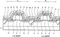
在图1和图5至19中,在左侧示出一个n沟道导电型MISFET(n型MISFET),而在右侧示出一个p沟道导电型MISFET(p型MISFET)。In FIG. 1 and FIGS. 5 to 19 , an n-channel conductivity type MISFET (n-type MISFET) is shown on the left side, and a p-channel conductivity type MISFET (p-type MISFET) is shown on the right side.
如图1中所示,根据本实施例的半导体器件具有一个半导体基片,其主要由例如单晶硅所制成的p型硅基片(在下文中简称为“p型基片”)所构成。p型基片1的电路形成表面(一个主表面)的上面具有nMIS形成区(第一元件形成区)1n和pMIS形成区(第二元件形成区)1p,并且nMIS形成区1n通过例如浅沟槽隔离(SGI)区4与pMIS形成区1p相分离。在nMIS形成区1n中,形成一个p型阱2和n沟道导电型MISFET(在下文简称为“n型MISFET”),而在pMIS形成区1p中形成一个n型阱区3和一个p沟道导电型MISFET(在下文中简称为“p型MISFET”)。通过在p型基片1的电路形成表面中制作一个浅沟槽,然后有选择地把一个绝缘膜(例如,氧化硅膜)嵌入在该浅沟槽内部而形成该浅沟槽隔离区4。本实施例的n型和p型MISFET分别具有允许电流在p型基片的平面方向上流动的水平结构。As shown in FIG. 1, the semiconductor device according to the present embodiment has a semiconductor substrate mainly composed of a p-type silicon substrate (hereinafter simply referred to as "p-type substrate") made of, for example, single crystal silicon. . The circuit formation surface (one main surface) of the p-type substrate 1 has an nMIS formation region (first element formation region) 1n and a pMIS formation region (second element formation region) 1p on it, and the nMIS formation region 1n passes through, for example, a shallow trench. Groove isolation (SGI) region 4 is separated from pMIS formation region 1p. In the nMIS formation region 1n, a p-type well 2 and an n-channel conduction type MISFET (hereinafter simply referred to as "n-type MISFET") are formed, while an n-type well region 3 and a p-channel are formed in the pMIS formation region 1p. channel conduction type MISFET (hereinafter simply referred to as "p-type MISFET"). The shallow trench isolation region 4 is formed by making a shallow trench in the circuit formation surface of the p-type substrate 1, and then selectively embedding an insulating film (for example, a silicon oxide film) inside the shallow trench. The n-type and p-type MISFETs of this embodiment each have a horizontal structure that allows current to flow in the plane direction of the p-type substrate.
n型MISFET主要具有一个沟道形成区、栅绝缘膜5、栅极6、侧壁衬垫9、源区和漏区。源区和漏区具有n型半导体区(扩展区)7和n型半导体区10。n型半导体区7被形成为与栅极6自对准,而n型半导体区10被形成为与置于栅极6的侧壁上的侧壁衬垫9自对准。n型半导体区10被形成为具有比n型半导体区7更高的杂质浓度。The n-type MISFET mainly has a channel formation region, gate insulating film 5, gate 6, side wall spacers 9, source and drain regions. The source and drain regions have n-type semiconductor regions (extension regions) 7 and n-type semiconductor regions 10 . N-type semiconductor region 7 is formed to be self-aligned with gate 6 , and n-type semiconductor region 10 is formed to be self-aligned with sidewall spacers 9 disposed on the sidewall of gate 6 . N-type semiconductor region 10 is formed to have a higher impurity concentration than n-type semiconductor region 7 .
p型MISFET主要具有一个沟道形成区、栅绝缘膜5、栅极6、侧壁衬垫9、源区和漏区。源区和漏区具有p型半导体区(扩展区)8和p型半导体区11。p型半导体区8被形成为与栅极6自对准,而p型半导体区11被形成为与置于栅极6的侧壁上的侧壁衬垫9自对准。p型半导体区11被形成为具有比p型半导体区8更高的杂质浓度。The p-type MISFET mainly has a channel formation region, gate insulating film 5, gate 6, side wall spacers 9, source and drain regions. The source and drain regions have p-type semiconductor regions (extension regions) 8 and p-type semiconductor regions 11 . The p-type semiconductor region 8 is formed to be self-aligned with the gate 6 , and the p-type semiconductor region 11 is formed to be self-aligned with the sidewall spacers 9 placed on the sidewall of the gate 6 . P-type semiconductor region 11 is formed to have a higher impurity concentration than p-type semiconductor region 8 .
在每个栅极6、n型半导体区10和p型半导体区11的表面上,形成有一个硅化物层(金属半导体反应层)12,以降低电阻。硅化物层12被置于栅极6的表面上,置于每个n型半导体区10和p型半导体区11的表面上的硅化物层被形成为与置于栅极6的侧壁上的侧壁衬垫9自对准。硅化物层12例如通过自对准硅化物(Self Aligned Silicide)技术而形成。本实施例的n型和p型MISFET分别具有自对齐硅化物结构。On the surface of each gate 6, n-type semiconductor region 10 and p-type semiconductor region 11, a silicide layer (metal-semiconductor reaction layer) 12 is formed to reduce resistance. A silicide layer 12 is placed on the surface of the gate 6, and the silicide layer placed on the surface of each of the n-type semiconductor region 10 and the p-type semiconductor region 11 is formed to be the same as that placed on the sidewall of the gate 6. The sidewall liners 9 are self-aligning. The silicide layer 12 is formed by, for example, self-aligned silicide (Self Aligned Silicide) technology. The n-type and p-type MISFETs of this embodiment respectively have self-aligned silicide structures.
在p型基片1的电路形成表面上,例如由一个氧化硅膜形成一个层间绝缘膜16。该层间绝缘膜16被形成为覆盖p型基片1的电路形成表面。在n型MISFET和层间绝缘膜16之间例如形成作为用于在p型基片1的电路形成表面上产生伸张应力的第一氮化物膜的氮化硅膜14a。在p型MISFET和层间绝缘膜16之间例如形成作为用于在p型基片1的电路形成表面上产生压缩应力的第二氮化物膜的氮化硅膜14b。在本实施例中,氮化硅膜14a被有选择地形成在n型MISFET上,以覆盖其栅极6,并且氮化硅膜14b被有选择地形成在p型MISFET上,以覆盖其栅极6。On the circuit-formed surface of the p-type substrate 1, an interlayer insulating film 16 is formed of, for example, a silicon oxide film. This interlayer insulating film 16 is formed to cover the circuit formation surface of the p-type substrate 1 . Between the n-type MISFET and the interlayer insulating film 16, for example, a silicon nitride film 14a is formed as a first nitride film for generating tensile stress on the circuit-forming surface of the p-type substrate 1. Between the p-type MISFET and the interlayer insulating film 16, for example, a silicon nitride film 14b is formed as a second nitride film for generating compressive stress on the circuit-forming surface of the p-type substrate 1. In this embodiment, the silicon nitride film 14a is selectively formed on the n-type MISFET to cover its gate 6, and the silicon nitride film 14b is selectively formed on the p-type MISFET to cover its gate. Pole 6.
在n型MISFET和氮化硅膜14a之间,以及在p型MISFET和氮化硅膜14b之间,形成例如由氧化硅膜所制成的绝缘膜13。该绝缘膜13被形成在p型基片1的电路形成表面上,以覆盖每个n型和p型MISFET。Between the n-type MISFET and the silicon nitride film 14a, and between the p-type MISFET and the silicon nitride film 14b, an insulating film 13 made of, for example, a silicon oxide film is formed. The insulating film 13 is formed on the circuit-forming surface of the p-type substrate 1 so as to cover each of the n-type and p-type MISFETs.
在氮化硅膜14a和层间绝缘膜16之间,形成例如由氧化硅膜所制成的绝缘膜15。该绝缘膜15有选择地形成在氮化硅膜14a上,以覆盖该氮化硅膜14a。Between the silicon nitride film 14a and the interlayer insulating film 16, an insulating film 15 made of, for example, a silicon oxide film is formed. The insulating film 15 is selectively formed on the silicon nitride film 14a so as to cover the silicon nitride film 14a.
在n型半导体区10和p型半导体区11上,形成从层间绝缘膜16的表面延伸到硅化物层12的用于源极-漏极的通孔18。在用于源极-漏极的通孔18内部,嵌入一个导电插塞19。该n型半导体区10和p型半导体区11分别通过硅化物层12和导电插塞19电连接到在层间绝缘膜16上延伸的一个互连层20。On the n-type semiconductor region 10 and the p-type semiconductor region 11, a via hole 18 for source-drain extending from the surface of the interlayer insulating film 16 to the silicide layer 12 is formed. Inside the via hole 18 for source-drain, a conductive plug 19 is embedded. The n-type semiconductor region 10 and the p-type semiconductor region 11 are electrically connected to an interconnection layer 20 extending on the interlayer insulating film 16 through the silicide layer 12 and the conductive plug 19, respectively.
尽管未示出,但是在栅极6上形成用于栅极的接触孔,该孔从层间绝缘膜16的表面延伸到硅化物层12。导电插塞19被嵌入在该栅极接触孔内部。该栅极6通过栅极接触孔内部的硅化物层12和导电插塞19电连接到在层间绝缘膜16上延伸的互连层20。Although not shown, a contact hole for a gate electrode extending from the surface of the interlayer insulating film 16 to the silicide layer 12 is formed on the gate electrode 6 . A conductive plug 19 is embedded inside the gate contact hole. The gate 6 is electrically connected to the interconnection layer 20 extending on the interlayer insulating film 16 through the silicide layer 12 and the conductive plug 19 inside the gate contact hole.
使用氮化硅膜14a、14b作为阻蚀层,通过SAC(自对准接触孔)技术分别形成源极-漏极接触孔18和栅极接触孔。换句话说,氮化硅膜14a、14b作为用于自对准接触的绝缘膜。Using the silicon nitride films 14a, 14b as etching resists, the source-drain contact hole 18 and the gate contact hole are respectively formed by the SAC (Self-Aligned Contact Hole) technique. In other words, the silicon nitride films 14a, 14b serve as insulating films for self-alignment contacts.
这些氮化硅膜14a、14b例如通过等离子体CVD(化学汽相淀积)方法而形成。通过改变这些氮化硅膜14a、14b的形成条件(反应气体、气压、温度、RF功率,等等)而控制要在p型基片1的电路形成表面上产生的应力。在本实施例中,通过在低至300到400W范围内的RF功率的条件下形成氮化硅膜14a而把在p型基片1的电路形成表面上产生的应力控制为伸张应力。另一方面,通过在高达600到700W范围内的RF功率的条件下形成氮化硅膜14b而把在p型基片1的电路形成表面上产生的应力控制为压缩应力。These silicon nitride films 14a, 14b are formed by, for example, a plasma CVD (Chemical Vapor Deposition) method. The stress to be generated on the circuit formation surface of the p-type substrate 1 is controlled by changing the formation conditions (reactive gas, gas pressure, temperature, RF power, etc.) of these silicon nitride films 14a, 14b. In this embodiment, the stress generated on the circuit-forming surface of the p-type substrate 1 is controlled to be tensile stress by forming the silicon nitride film 14a under the condition of RF power as low as in the range of 300 to 400W. On the other hand, the stress generated on the circuit-formed surface of the p-type substrate 1 is controlled as compressive stress by forming the silicon nitride film 14b under the condition of RF power as high as in the range of 600 to 700W.
分别通过上述方法,从大约+700至+800Mpa的伸张应力存在于氮化硅膜14a中,并且从大约-900至-1000Mpa压缩应力存在于氮化硅膜14a中,从而伸张应力出现在n型MISFET的沟道形成区中,并且压缩应力出现在p型MISFET的沟道形成区中,与不被氮化硅膜14a、14b所覆盖的情况相比,导致使n型MISFET的漏极电流提高10至15%,以及p型MISFET的漏极电流提高15至20%。如上文所述,这些应力被施加在与漏极电流(Id)流过沟道形成区的方向(即,栅极长度方向)相类似的方向上。By the above methods respectively, tensile stress from about +700 to +800 MPa exists in the silicon nitride film 14a, and compressive stress exists in the silicon nitride film 14a from about -900 to -1000 MPa, so that the tensile stress appears in the n-type In the channel formation region of the MISFET, and compressive stress occurs in the channel formation region of the p-type MISFET, compared with the case where it is not covered with the silicon nitride films 14a, 14b, resulting in an increase in the drain current of the n-type MISFET 10 to 15%, and a 15 to 20% increase in the drain current of the p-type MISFET. As described above, these stresses are applied in a direction similar to the direction in which the drain current (Id) flows through the channel formation region (ie, the gate length direction).
下面使用与本实施例中所用的附图略有不同的简化附图和参考标号描述在MISFET的沟道形成区中出现的应力。图3和4中所示的MISFET具有类似于本实施例的硅化物结构。在标号30所示的是MISFET的沟道形成区,31为漏极电流流过沟道形成区30的方向,32为被形成为与栅极6对准的半导体区,33为被形成为与侧壁衬垫9相对准的半导体区,34为用于在沟道形成区30中产生应力的薄膜,以及35a和35b分别为一个台阶部分。The stress occurring in the channel formation region of the MISFET is described below using simplified drawings and reference numerals slightly different from those used in this embodiment. The MISFET shown in FIGS. 3 and 4 has a silicide structure similar to that of this embodiment. Indicated at 30 is a channel forming region of the MISFET, 31 is a direction in which a drain current flows through the channel forming region 30, 32 is a semiconductor region formed to be aligned with the gate 6, and 33 is formed to be aligned with the gate 6. The sidewall spacer 9 is aligned with the semiconductor region, 34 is a thin film for generating stress in the channel formation region 30, and 35a and 35b are each a stepped portion.
如图3和4中所示,MISFET具有置于栅极6的侧壁上的侧壁衬垫9,以包围栅极6。该栅极6和侧壁衬垫9从该栅极凸出,从而由它们形成台阶部分(35a、35b)。当薄膜34形成在这样一个结构的MISFET上以覆盖栅极6,从而在沟道形成区30中产生应力(伸张应力或压缩应力)时,应力集中在栅极长度方向X中所存在的台阶部分35a的跟脚上,以及集中在栅极宽度方向Y中所存在的台阶部分35b的跟脚上,从而从存在于栅极长度方向X的台阶部分35a的跟脚开始在栅极长度方向上的薄膜应力作用在沟道形成区30上,同时从存在于栅极宽度方向Y的台阶部分35b的跟脚开始在栅极宽度方向上的薄膜应力作用在沟道形成区30上。换句话说,当薄膜34的应力为伸张应力时,该伸张应力在栅极长度方向和栅极宽度方向上出现在沟道形成区30中,并且当薄膜34的应力为压缩应力时,该压缩应力在栅极长度方向和栅极宽度方向上出现在沟道形成区30中。As shown in FIGS. 3 and 4 , the MISFET has a sidewall spacer 9 placed on the sidewall of the gate 6 so as to surround the gate 6 . The gate 6 and side wall spacers 9 protrude from the gate so that stepped portions (35a, 35b) are formed by them. When the thin film 34 is formed on the MISFET of such a structure to cover the gate 6, thereby generating stress (tensile stress or compressive stress) in the channel formation region 30, the stress concentrates on the stepped portion existing in the gate length direction X 35a, and concentrated on the heel of the step portion 35b existing in the gate width direction Y, so that starting from the heel of the step portion 35a existing in the gate length direction X in the gate length direction The film stress acts on the channel formation region 30 while the film stress acts on the channel formation region 30 in the gate width direction from the heel of the step portion 35b existing in the gate width direction Y. In other words, when the stress of the thin film 34 is tensile stress, the tensile stress appears in the channel formation region 30 in the gate length direction and the gate width direction, and when the stress of the thin film 34 is compressive stress, the compressive stress Stress occurs in the channel formation region 30 in the gate length direction and the gate width direction.
在栅极长度方向X中的栅极6的长度远小于在该栅极宽度方向Y上的长度,从而在栅极宽度方向上的伸张应力或压缩应力显著地减小,该应力是通过在栅极宽度方向Y上集中在台阶部分35b的跟脚处的伸张应力或压缩应力而出现在沟道形成区30中的应力。相应地,在沟道形成区30中由薄膜34所产生的应力可以仅仅被认为是在栅极长度方向上的伸张应力或压缩应力,换句话说,作为沿着漏极电流方向31的伸张应力或压缩应力。The length of the gate 6 in the gate length direction X is much smaller than the length in the gate width direction Y, so that the tensile stress or compressive stress in the gate width direction is significantly reduced. The stress occurring in the channel formation region 30 is the tensile stress or the compressive stress concentrated at the heel of the step portion 35 b in the pole width direction Y. Accordingly, the stress generated by the thin film 34 in the channel formation region 30 can be regarded only as a tensile stress or a compressive stress in the gate length direction, in other words, as a tensile stress along the drain current direction 31 or compressive stress.
有报告表明,当在栅极宽度方向上的压缩应力被施加到沟道形成区30上时,在p型MISFET中出现漏极电流的减小。对于通过薄膜34对沟道形成区30上的应力进行控制,可以有效地增加p型MISFET的漏极电流,由于如上文所述,作为在沟道形成区30中出现的应力的在栅极宽度方向上的栅极应力被显著减小。因此,由薄膜34进行沟道形成区30的应力控制对于p场效应晶体管来说特别有效。It has been reported that when a compressive stress in the gate width direction is applied to the channel formation region 30, a decrease in drain current occurs in a p-type MISFET. For controlling the stress on the channel forming region 30 through the thin film 34, the drain current of the p-type MISFET can be effectively increased, because as described above, as the stress occurring in the channel forming region 30 in the gate width The gate stress in the direction is significantly reduced. Therefore, stress control of the channel formation region 30 by the thin film 34 is particularly effective for p field effect transistors.
由于当薄膜应力的开始点与沟道形成区30相分离时通过薄膜34的应力而在沟道形成区30中造成的应力减小,因此需要把薄膜应力的开始点尽可能地接近于沟道形成区30。在上文所述中,应力从由栅极6和侧壁衬垫9所产生的台阶部分(35a、35b)的跟脚处开始。在没有侧壁衬垫9的MISFET的情况中,栅极6的每个侧壁的跟脚变为薄膜应力的开始点。Since the stress caused in the channel forming region 30 by the stress of the film 34 is reduced when the starting point of the film stress is separated from the channel forming region 30, it is necessary to place the starting point of the film stress as close to the channel as possible. Zone 30 is formed. In the above, the stress starts from the heel of the stepped portion ( 35 a , 35 b ) generated by the gate electrode 6 and the sidewall spacer 9 . In the case of the MISFET without the sidewall spacer 9, the heel of each sidewall of the gate 6 becomes a starting point of film stress.
下面根据图5至19描述实施例1的半导体器件的制造方法。A method of manufacturing the semiconductor device of Embodiment 1 will be described below with reference to FIGS. 5 to 19 .
首先,准备由具有10Ωcm的电阻率的单晶硅所制成的p型基片1,并且在p型基片1的电路形成表面上,有选择地形成p型阱区2和n型阱区3,如图5中所示。First, a p-type substrate 1 made of single-crystal silicon having a resistivity of 10 Ωcm is prepared, and a p-type well region 2 and an n-type well region are selectively formed on the circuit formation surface of the p-type substrate 1 3, as shown in Figure 5.
然后,如图5中所示,一个浅沟槽隔离区4被形成在p型基片1的电路形成表面上,用于使nMIS形成区(第一元件形成区)1n与pMIS形成区(第二元件形成区)1p相分离的一个元件隔离区域。通过在p型基片1的电路形成表面上形成一个浅沟槽(例如,大约300[nm]深的沟槽),通过CVD方法在p型基片1的电路形成表面上形成一个氧化硅膜作为绝缘膜,然后通过CMP(化学机械抛光)方法对该绝缘膜进行平面化,仅仅把它保留在该浅沟槽内,从而形成该浅沟槽隔离区4。Then, as shown in FIG. 5, a shallow trench isolation region 4 is formed on the circuit formation surface of the p-type substrate 1 for making the nMIS formation region (first element formation region) 1n and the pMIS formation region (the first element formation region) 1n An element isolation region separated from two element forming regions) 1p. By forming a shallow trench (for example, about 300 [nm] deep trench) on the circuit formation surface of the p-type substrate 1, a silicon oxide film is formed on the circuit formation surface of the p-type substrate 1 by the CVD method As an insulating film, the insulating film is then planarized by a CMP (Chemical Mechanical Polishing) method, leaving it only in the shallow trench, thereby forming the shallow trench isolation region 4 .
如图6中所示,通过热处理在p型基片1的电路形成表面上的nMIS形成区1n和pMIS形成区1p中形成大约2-3纳米后的氧化硅膜所制成的栅极绝缘膜5。然后,通过CVD方法在p型基片1的整个电路形成表面上形成大约150至200nm厚的多晶硅膜,然后通过对该多晶硅膜进行构图而形成栅极6。在淀积多晶硅膜过程中或之后,导入减小电阻的杂质。As shown in FIG. 6, the gate insulating film made by heat-treating the silicon oxide film formed by about 2-3 nm in the nMIS formation region 1n and the pMIS formation region 1p on the circuit formation surface of the p-type substrate 1 5. Then, a polysilicon film of approximately 150 to 200 nm thick is formed on the entire circuit-forming surface of the p-type substrate 1 by the CVD method, and then the gate electrode 6 is formed by patterning the polysilicon film. Impurities that reduce resistance are introduced during or after the deposition of the polysilicon film.
如图6中所示,通过离子注入有选择地把例如砷(As)这样的杂质导入到没有栅极6的p型阱区2的区域中而形成一对n型半导体区(扩展区)7,随后通过离子注入有选择地把例如二氟化硼(BF2)这样的杂质导入到没有栅极6的n型阱区3的一个区域中而形成一对p型半导体区(扩展区)8。当pMIS形成区1p被光刻胶掩膜所覆盖时形成n型半导体区7,当nMIS形成区1n被光刻胶掩膜所覆盖时形成p型半导体区8。在1-5KeV的加速能量和1至2×10¹⁵/cm2的剂量的条件下导入砷。在1-5KeV的加速能量和1至2×1015/cm2的剂量的条件下导入二氟化硼。n型半导体区7和p型半导体区8被分别形成为与栅极6相对准。As shown in FIG. 6, a pair of n-type semiconductor regions (extension regions) 7 are formed by selectively introducing impurities such as arsenic (As) into the region of the p-type well region 2 without the gate 6 by ion implantation. , followed by selectively introducing an impurity such as boron difluoride (BF2 ) into a region of the n-type well region 3 without the gate 6 by ion implantation to form a pair of p-type semiconductor regions (extension regions) 8 . The n-type semiconductor region 7 is formed when the pMIS formation region 1p is covered by the photoresist mask, and the p-type semiconductor region 8 is formed when the nMIS formation region 1n is covered by the photoresist mask. Arsenic is introduced under conditions of an acceleration energy of 1-5 KeV and a dose of 1 to 2×10¹⁵ /cm2 . Boron difluoride is introduced under conditions of an acceleration energy of 1-5 KeV and a dose of 1 to 2×10¹⁵ /cm2 . The n-type semiconductor region 7 and the p-type semiconductor region 8 are respectively formed to be aligned with the gate 6 .
在导入杂质以形成半导体区(7,8)之后,通过热处理激活这些半导体区(7,8)。After introducing impurities to form semiconductor regions (7, 8), these semiconductor regions (7, 8) are activated by heat treatment.
如图6中所示,例如在栅极长度方向上具有大约50-70nm厚度的侧壁衬垫9被形成在栅极6的侧壁上。例如通过CVD方法在p型基片1的整个电路形成表面上形成由氧化硅膜和氮化硅膜所制成的绝缘膜而形成这些侧壁衬垫9,然后使该绝缘膜受到各向异性蚀刻,例如RIE(反应离子蚀刻)。这些侧壁衬垫9被形成为与栅极6相对准。As shown in FIG. 6 , a sidewall spacer 9 having a thickness of, for example, about 50-70 nm in the gate length direction is formed on the sidewall of the gate electrode 6 . These side wall spacers 9 are formed, for example, by forming an insulating film made of silicon oxide film and silicon nitride film on the entire circuit formation surface of the p-type substrate 1 by a CVD method, and then subjecting the insulating film to anisotropy. Etching, eg RIE (Reactive Ion Etching). These sidewall spacers 9 are formed in alignment with the gates 6 .
如图6中所示,通过离子注入有选择地把例如砷(As)这样的杂质导入到没有栅极6的p型阱区2的区域中而形成一对n型半导体区10,随后通过离子注入有选择地把例如二氟化硼(BF2)这样的杂质导入到没有栅极6的n型阱区3的一个区域中而形成一对p型半导体区11。当pMIS形成区1p被光刻胶掩膜所覆盖时形成n型半导体区10,当nMIS形成区1n被光刻胶掩膜所覆盖时形成p型半导体区11。在35-45KeV的加速能量和2至4×10¹⁵/cm2的剂量的条件下导入砷。在40-50KeV的加速能量和2至4×1015/cm2的剂量的条件下导入二氟化硼。n型半导体区10和p型半导体区11被分别形成为与侧壁衬垫9相对准。As shown in FIG. 6, a pair of n-type semiconductor regions 10 are formed by selectively introducing impurities such as arsenic (As) into the region of the p-type well region 2 without the gate 6 by ion implantation, followed by ion implantation. Implantation selectively introduces an impurity such as boron difluoride (BF2 ) into a region of the n-type well region 3 without the gate 6 to form a pair of p-type semiconductor regions 11 . The n-type semiconductor region 10 is formed when the pMIS formation region 1p is covered by the photoresist mask, and the p-type semiconductor region 11 is formed when the nMIS formation region 1n is covered by the photoresist mask. Arsenic is introduced under the conditions of an acceleration energy of 35-45 KeV and a dose of 2 to 4×10¹⁵ /cm2 . Boron difluoride is introduced under the conditions of an acceleration energy of 40-50 KeV and a dose of 2 to 4×10¹⁵ /cm2 . The n-type semiconductor region 10 and the p-type semiconductor region 11 are respectively formed to be aligned with the sidewall spacers 9 .
在导入杂质以形成半导体区(10,11)之后,通过热处理激活这些半导体区(10,11)。After introducing impurities to form semiconductor regions (10, 11), these semiconductor regions (10, 11) are activated by heat treatment.
通过上述步骤,形成具有与栅极6相对准的n型半导体区7以及与侧壁衬垫9相对准的n型半导体区10的源区和漏区;以及形成具有与栅极6相对准的p型半导体区8以及与侧壁衬垫9相对准的p型半导体区11的源区和漏区。因此,形成水平的n型和p型MISFET。Through the above steps, a source region and a drain region having an n-type semiconductor region 7 aligned with the gate 6 and an n-type semiconductor region 10 aligned with the sidewall spacer 9 are formed; The p-type semiconductor region 8 and the source and drain regions of the p-type semiconductor region 11 aligned with the sidewall liner 9 . Thus, horizontal n-type and p-type MISFETs are formed.
在通过除去自然氧化膜而暴露栅极6和半体导区域(10,11)的表面之后,执行溅射,以在包括这些表面的p型基片1的整个电路形成表面上形成一个钴(Co)膜12a,如图7中所示。然后,如图8中所示,执行热处理,使得栅极6的硅(Si)与钴膜12的Co发生反应,从而在栅极6的表面上形成硅化物(CoSix)层12,作为金属半导体反应层;同时,使得半导体区(10,11)的硅(Si)与钴膜12a的Co发生反应,从而在半导体区(10,11)的表面上形成硅化物(CoSix)层12。如图9中所示,钴膜12a的未反应部分被有选择地从不形成硅化物层12的一个区域上除去,随后通过热处理激活硅化物层12。After exposing the surfaces of the gate 6 and the semiconductor region (10, 11) by removing the natural oxide film, sputtering is performed to form a cobalt ( Co) film 12a, as shown in FIG. 7 . Then, as shown in FIG. 8, heat treatment is performed so that silicon (Si) of the gate 6 reacts with Co of the cobalt film 12, thereby forming a silicide (CoSix ) layer 12 on the surface of the gate 6 as a metal Semiconductor reaction layer; at the same time, the silicon (Si) in the semiconductor region (10, 11) reacts with the Co in the cobalt film 12a, thereby forming a silicide (CoSix ) layer 12 on the surface of the semiconductor region (10, 11). As shown in FIG. 9, an unreacted portion of the cobalt film 12a is selectively removed from a region where the silicide layer 12 is not formed, and then the silicide layer 12 is activated by heat treatment.
通过上述步骤,被淀积在栅极6的表面上的硅化物层12和淀积在半导体区(10,11)上的硅化物层12被形成为与侧壁衬垫9相对准。因此,形成具有自对齐硅化物结构的n型和p型MISFET。Through the above steps, the silicide layer 12 deposited on the surface of the gate electrode 6 and the silicide layer 12 deposited on the semiconductor regions ( 10 , 11 ) are formed to be aligned with the sidewall spacers 9 . Thus, n-type and p-type MISFETs having a salicide structure are formed.
如图10中所示,通过CVD方法在包括n型和p型MISFET的p型基片1的整个电路形成表面上形成例如由大约5-10nm厚的氧化硅膜所制成的绝缘膜13。通过该步骤,栅极6的硅化物层12、半导体区(10,11)的硅化物层12以及侧壁衬垫9被绝缘膜13所覆盖。As shown in FIG. 10, an insulating film 13 made of, for example, a silicon oxide film about 5-10 nm thick is formed by the CVD method on the entire circuit-forming surface of the p-type substrate 1 including n-type and p-type MISFETs. Through this step, the silicide layer 12 of the gate electrode 6 , the silicide layer 12 of the semiconductor region ( 10 , 11 ), and the side wall spacer 9 are covered with the insulating film 13 .
如图11中所示,通过等离子体CVD方法形成大约100至120nm厚的氮化硅膜14a,作为在包括n型和p型MISFET的p型基片1的整个电路形成表面上的绝缘膜。氮化硅膜14a例如在350至400W的RF功率或300至350乇的腔内气压的条件下形成。As shown in FIG. 11, a silicon nitride film 14a of about 100 to 120 nm thick is formed by the plasma CVD method as an insulating film on the entire circuit formation surface of the p-type substrate 1 including n-type and p-type MISFETs. The silicon nitride film 14a is formed, for example, under the conditions of an RF power of 350 to 400 W or a chamber pressure of 300 to 350 Torr.
通过上述步骤,n型和p型MISFET被氮化硅膜14a所覆盖,并且栅极6的硅化物层12、半导体区(10,11)和侧壁衬垫9隔着绝缘膜13被氮化硅膜14a所覆盖。Through the above steps, the n-type and p-type MISFETs are covered by the silicon nitride film 14a, and the silicide layer 12 of the gate 6, the semiconductor regions (10, 11) and the side wall spacers 9 are nitrided through the insulating film 13 covered by a silicon film 14a.
如图12中所示,通过CVD方法在包括n型和p型MISFET的上表面的p型基片1的整个电路形成表面上形成大约50nm厚的氧化硅膜所制成的绝缘膜15。通过该步骤,氮化硅膜14a被绝缘膜15所覆盖。As shown in FIG. 12, an insulating film 15 made of a silicon oxide film about 50 nm thick is formed by the CVD method on the entire circuit formation surface of the p-type substrate 1 including the upper surfaces of the n-type and p-type MISFETs. Through this step, the silicon nitride film 14a is covered with the insulating film 15 .
如图13中所示,有选择地覆盖nMIS形成区1n(n型MISFET)的上表面的光刻胶掩膜RM1被形成在绝缘膜15上。As shown in FIG. 13 , a resist mask RM1 selectively covering the upper surface of the nMIS formation region 1n (n-type MISFET) is formed on the insulating film 15 .
通过利用该光刻胶掩膜RM1作为蚀刻掩膜,通过蚀刻而顺序地从pMIS形成区1p的上表面(p型MISFET的上表面)上除去绝缘膜15和氮化硅膜14a。为了除去绝缘膜15和氮化硅膜14a,分别采用湿法蚀刻和各向同性干法蚀刻方法。By using this resist mask RM1 as an etching mask, the insulating film 15 and the silicon nitride film 14a are sequentially removed from the upper surface of the pMIS formation region 1p (the upper surface of the p-type MISFET) by etching. In order to remove the insulating film 15 and the silicon nitride film 14a, wet etching and isotropic dry etching methods are employed, respectively.
通过上述步骤,氮化硅膜14a被有选择地形成在n型MISFET上,以覆盖其栅极6。由于按照上述方式有选择地形成氮化硅膜14a,因此有选择地在n型MISFET的沟道形成区中产生伸张应力。Through the above steps, the silicon nitride film 14a is selectively formed on the n-type MISFET so as to cover the gate 6 thereof. Since the silicon nitride film 14a is selectively formed in the above-described manner, tensile stress is selectively generated in the channel formation region of the n-type MISFET.
并且通过该步骤,由于这些硅化物层12和侧壁衬垫9被绝缘膜13所覆盖,因此可以抑制在除去过程中由于过蚀刻而导致不可避免地腐蚀在栅极6表面上的硅化物层12、p型半导体区11的表面上的硅化物层12以及侧壁衬垫9的情况。简而言之,绝缘膜13作为在除去氮化硅膜14a时的阻蚀层。And through this step, since these silicide layers 12 and the sidewall liners 9 are covered by the insulating film 13, it is possible to suppress the inevitable corrosion of the silicide layer on the surface of the gate 6 due to overetching during the removal process. 12. Situation of the silicide layer 12 and the sidewall liner 9 on the surface of the p-type semiconductor region 11 . In short, the insulating film 13 serves as an etching stopper when the silicon nitride film 14a is removed.
如果在该步骤中没有绝缘膜13,则由于在除去时对氮化硅膜14a的过蚀刻而出现问题。下面将描述这种问题。If there is no insulating film 13 in this step, a problem arises due to overetching of the silicon nitride film 14a upon removal. Such a problem will be described below.
如图15中所示,在除去光刻胶掩膜RM1之后,通过等离子CVD方法在包括绝缘膜15的上表面的p型基片1的整个电路形成表面上形成大约100nm厚的氮化硅膜14b,作为绝缘膜。氮化硅膜14b例如在600至700W的RF功率或5至10乇的腔内气压的条件下形成。As shown in FIG. 15, after removing the photoresist mask RM1, a silicon nitride film about 100 nm thick is formed by the plasma CVD method on the entire circuit formation surface of the p-type substrate 1 including the upper surface of the insulating film 15. 14b, as an insulating film. The silicon nitride film 14b is formed, for example, under the conditions of an RF power of 600 to 700 W or a chamber pressure of 5 to 10 Torr.
通过上述步骤,n型和p型MISFET被氮化硅膜14b所覆盖,并且在n型MISFET上的氮化硅膜14a隔着绝缘膜15被氮化硅膜14b所覆盖。Through the above steps, the n-type and p-type MISFETs are covered with the silicon nitride film 14b, and the silicon nitride film 14a on the n-type MISFET is covered with the silicon nitride film 14b via the insulating film 15.
如图16中所示,有选择地覆盖pMIS形成区1p(p型MISFET)的上表面的光刻胶掩膜RM2被形成在氮化硅膜14b上。As shown in FIG. 16, a photoresist mask RM2 selectively covering the upper surface of the pMIS formation region 1p (p-type MISFET) is formed on the silicon nitride film 14b.
通过利用该光刻胶掩膜RM2作为蚀刻掩膜,通过蚀刻而从nMIS形成区1n的上表面(n型MISFET的上表面)上除去氮化硅膜14b。氮化硅膜14b被各向同性干法蚀刻方法所除去。By using this resist mask RM2 as an etching mask, the silicon nitride film 14b is removed from the upper surface of the nMIS formation region 1n (the upper surface of the n-type MISFET) by etching. The silicon nitride film 14b is removed by isotropic dry etching.
通过上述步骤,氮化硅膜14b被有选择地形成在p型MISFET上,以覆盖其栅极6。由于按照上述方式有选择地形成氮化硅膜14b,因此有选择地在p型MISFET的沟道形成区中产生压缩应力。Through the above steps, the silicon nitride film 14b is selectively formed on the p-type MISFET so as to cover the gate 6 thereof. Since the silicon nitride film 14b is selectively formed in the above-described manner, compressive stress is selectively generated in the channel formation region of the p-type MISFET.
通过该步骤,由于在n型MISFET上的氮化硅膜14a被绝缘膜15所覆盖,因此可以抑制在除去氮化硅膜14b的过程中由于过蚀刻而导致除去氮化硅膜14a的不便。简而言之,绝缘膜15作为在除去氮化硅膜14b时的阻蚀层。Through this step, since the silicon nitride film 14a on the n-type MISFET is covered with the insulating film 15, the inconvenience of removing the silicon nitride film 14a due to overetching during removal of the silicon nitride film 14b can be suppressed. In short, the insulating film 15 serves as an etching stopper when the silicon nitride film 14b is removed.
在除去光刻胶掩膜RM2之后,通过等离子体CVD方法在包括如图18中所示的n型和p型MISFET的上表面的p型基片1的整个电路形成表面上形成由氧化硅膜所制成的层间绝缘膜16,随后通过CMP方法对层间绝缘膜16的表面进行平面化。After removing the photoresist mask RM2, a silicon oxide film is formed on the entire circuit-forming surface of the p-type substrate 1 including the upper surfaces of the n-type and p-type MISFETs as shown in FIG. 18 by the plasma CVD method. The interlayer insulating film 16 is formed, and then the surface of the interlayer insulating film 16 is planarized by the CMP method.
如图18中所示,例如Ar、Ge、Si、As、Sb、In或BF2这样的杂质17被导入层间绝缘膜16,以破坏层间绝缘膜16的结晶性。在该步骤中,层间绝缘膜16的应力被释放,因此可以抑制层间绝缘膜16的应力对MISFET的沟道形成区的影响。当观察层间绝缘膜16的截面时,清楚地保留破坏的痕迹。As shown in FIG. 18 , impurities 17 such as Ar, Ge, Si, As, Sb, In, or BF2 are introduced into interlayer insulating film 16 to destroy the crystallinity of interlayer insulating film 16 . In this step, the stress of the interlayer insulating film 16 is released, so the influence of the stress of the interlayer insulating film 16 on the channel formation region of the MISFET can be suppressed. When the cross-section of interlayer insulating film 16 is observed, traces of destruction clearly remain.
如图19中所示,然后在半导体区(11,12)上形成从层间绝缘膜16的表面延伸到硅化物层12的源极-漏极接触孔18。这些源极-漏极接触孔18由SAC技术使用氮化硅膜(14a、14b)作为阻蚀层而形成。具体来说,具有用于该接触孔的开孔图案的光刻胶掩膜被形成在层间绝缘膜16上处于与半导体区(10,11)相对的位置处。利用该光刻胶掩膜作为蚀刻掩膜,通过各向异性蚀刻顺序地蚀刻层间绝缘膜16、绝缘膜15、氮化硅膜(14a、14b)和绝缘膜13。在使得层间绝缘膜16和绝缘膜15对氮化硅膜(14a、14b)具有蚀刻选择性的条件下对层间绝缘膜16和绝缘膜15进行蚀刻。在使得氮化硅膜(14a、14b)对绝缘膜13具有蚀刻选择性的条件下对氮化硅膜(14a、14b)进行蚀刻。在使得绝缘膜13对硅化物层12和p型基片1具有蚀刻选择性的条件下对绝缘膜13进行蚀刻。在除去氮化硅膜(14a、14b)之后,绝缘膜13可能被过蚀刻。As shown in FIG. 19, a source-drain contact hole 18 extending from the surface of the interlayer insulating film 16 to the silicide layer 12 is then formed on the semiconductor region (11, 12). These source-drain contact holes 18 are formed by the SAC technique using the silicon nitride film (14a, 14b) as an etching resist. Specifically, a photoresist mask having an opening pattern for the contact hole is formed on the interlayer insulating film 16 at a position opposed to the semiconductor region (10, 11). Using this resist mask as an etching mask, the interlayer insulating film 16, the insulating film 15, the silicon nitride films (14a, 14b), and the insulating film 13 are sequentially etched by anisotropic etching. The interlayer insulating film 16 and the insulating film 15 are etched under conditions such that the interlayer insulating film 16 and the insulating film 15 have etching selectivity to the silicon nitride film (14a, 14b). The silicon nitride films ( 14 a , 14 b ) are etched under conditions such that the silicon nitride films ( 14 a , 14 b ) have etching selectivity to the insulating film 13 . The insulating film 13 is etched under conditions such that the insulating film 13 has etching selectivity to the silicide layer 12 and the p-type substrate 1 . After removing the silicon nitride film (14a, 14b), the insulating film 13 may be over-etched.
按照与形成源极-漏极接触孔18的方法相类似的方法,从层间绝缘膜16的表面延伸到硅化物层12的栅极接触孔被形成在栅极6上,但是这未在图中示出。According to a method similar to the method of forming the source-drain contact hole 18, a gate contact hole extending from the surface of the interlayer insulating film 16 to the silicide layer 12 is formed on the gate electrode 6, but this is not shown in FIG. shown in .
然后,通过在源极-漏极接触孔18的内部和栅极接触孔的内部嵌入导电材料,接着在层间绝缘膜16上形成互连层20而形成一个导电插塞19,从而可以形成如图1中所示的结构。Then, a conductive plug 19 is formed by embedding a conductive material inside the source-drain contact hole 18 and inside the gate contact hole, followed by forming an interconnection layer 20 on the interlayer insulating film 16, so that a conductive plug 19 can be formed such as The structure shown in Figure 1.
在下面,将描述本发明以及在本发明的开发过程中由本发明人所发现的问题。In the following, the present invention and problems discovered by the present inventors during the development of the present invention will be described.
由于在执行各向异性干法蚀刻时沿着侧壁衬垫9的侧壁延伸的氮化硅膜14a看起来很厚,因此在通过各向异性干法蚀刻除去在p型MISFET上的氮化硅膜14a之后,一部分氮化硅膜14a被保留在侧壁衬垫9的侧壁上,如图20中所示。如果氮化硅膜14b被形成在p型MISFET上而不除去氮化硅膜14a的部分,则氮化硅膜14b的应力集中在由栅极6、侧壁衬垫9和如图21中所示的氮化硅膜14a的部分所形成的台阶部分35a的跟脚处,由于保留在侧壁衬垫9的侧壁上的氮化硅膜14a使得氮化硅膜14b的应力开始点与p型MISFET的沟道形成区相分离,从而减小用于在沟道形成区中产生压缩应力的氮化硅膜14b的应力的影响。另外,具有相反应力作用的氮化硅膜14a被保留在侧壁衬垫9的侧壁上,从而进一步减小用于在沟道形成区中产生压缩应力的氮化硅膜14b的影响。因此通过不会在台阶部分形成蚀刻剩余物的各向同性干法蚀刻而从p型MISFET有效地除去氮化硅膜14a。Since the silicon nitride film 14a extending along the sidewall of the sidewall spacer 9 appears thick when anisotropic dry etching is performed, the silicon nitride film 14a on the p-type MISFET is removed by anisotropic dry etching. After the silicon film 14a, a part of the silicon nitride film 14a is left on the side wall of the side wall spacer 9, as shown in FIG. If the silicon nitride film 14b is formed on the p-type MISFET without removing part of the silicon nitride film 14a, the stress of the silicon nitride film 14b is concentrated in the At the heel of the step portion 35a formed by the portion of the silicon nitride film 14a shown, since the silicon nitride film 14a remaining on the sidewall of the sidewall liner 9 makes the stress initiation point of the silicon nitride film 14b and p The channel formation region of the type MISFET is separated, thereby reducing the influence of the stress of the silicon nitride film 14b for generating compressive stress in the channel formation region. In addition, the silicon nitride film 14a having an opposite stress effect is left on the sidewall of the sidewall spacer 9, thereby further reducing the influence of the silicon nitride film 14b for generating compressive stress in the channel formation region. The silicon nitride film 14a is thus efficiently removed from the p-type MISFET by isotropic dry etching that does not form etching residues at the stepped portion.
但是从p型MISFET的上部除去氮化硅膜14a的各向同性干法蚀刻具有另一个问题。But the isotropic dry etching to remove the silicon nitride film 14a from the upper part of the p-type MISFET has another problem.
为了进行氮化硅膜的各向同性蚀刻,通常采用例如CF4和CF6这样的氟化物气体。在各向同性蚀刻时,氮化硅膜相对于氧化硅膜或硅化物层具有蚀刻选择性,但是对于硅没有蚀刻选择性。For isotropic etching of silicon nitride films, fluoride gases such as CF4 and CF6 are generally used. In isotropic etching, a silicon nitride film has etching selectivity to a silicon oxide film or a silicide layer, but has no etching selectivity to silicon.
在氮化硅膜14a的各向同性等离子体蚀刻时,氮化硅膜14a相对于由氧化硅膜所制成的侧壁衬垫9具有蚀刻选择性,但是在除去氮化硅膜14a时,该侧壁衬垫9被少量地蚀刻,从而侧壁衬垫9的整体膜厚向着栅极6的方向减小。在p型半导体区11的表面上的硅化物层12被形成为与侧壁衬垫9相对准。通过在除去氮化硅膜14a时的过蚀刻而减小侧壁衬垫的膜厚,不可避免地在侧壁衬垫9和硅化物层12之间形成硅的暴露部分al。在氮化硅膜的各向同性等离子体蚀刻,它对硅没有蚀刻选择性,从而由于在除去氮化硅膜14a时的过蚀刻使得p型基片1被从暴露部分1a蚀刻,造成例如栅极6剥离这样的问题。At the time of isotropic plasma etching of the silicon nitride film 14a, the silicon nitride film 14a has etching selectivity with respect to the side wall liner 9 made of a silicon oxide film, but when the silicon nitride film 14a is removed, The sidewall spacer 9 is slightly etched so that the overall film thickness of the sidewall spacer 9 decreases toward the gate 6 . Silicide layer 12 on the surface of p-type semiconductor region 11 is formed in alignment with sidewall spacer 9 . By reducing the film thickness of the sidewall spacer by overetching when removing the silicon nitride film 14a, an exposed portion a1 of silicon is inevitably formed between the sidewall spacer 9 and the silicide layer 12. In the isotropic plasma etching of the silicon nitride film, it has no etching selectivity to silicon, so that the p-type substrate 1 is etched from the exposed portion 1a due to overetching when the silicon nitride film 14a is removed, resulting in, for example, gate Pole 6 stripped such a problem.
在各向同性等离子体蚀刻时,氮化硅膜14a对硅化物层12具有蚀刻选择性,但是在除去氮化硅膜14a时的过蚀刻使得硅化物层12被少量地蚀刻,并且硅化物层12的厚度减小。硅化物层12被淀积在栅极6的表面上或者p型半导体区11的表面上,以抑制由于MISFET的小型化而导致栅极电阻增加或源极-漏极电流增加。当由于在除去氮化硅膜14a时的过蚀刻而导致硅化物层12的厚度减小时,不可避免地降低抑制由于MISFET的小型化所导致栅极电阻增加或源极-漏极电流增加的效果。At the time of isotropic plasma etching, the silicon nitride film 14a has etching selectivity to the silicide layer 12, but the overetching at the time of removing the silicon nitride film 14a causes the silicide layer 12 to be slightly etched, and the silicide layer 12 is reduced in thickness. Silicide layer 12 is deposited on the surface of gate 6 or on the surface of p-type semiconductor region 11 to suppress an increase in gate resistance or an increase in source-drain current due to miniaturization of the MISFET. When the thickness of the silicide layer 12 is reduced due to overetching at the time of removing the silicon nitride film 14a, the effect of suppressing an increase in gate resistance or an increase in source-drain current due to miniaturization of the MISFET is inevitably lowered. .
在具有自对齐硅化物结构的p型MISFET的情况中,由于硅化物层12作为阻蚀层,因此在除去氮化硅膜14a时,在栅极6的硅化物层12下方的多晶硅膜和源极-漏极区的硅化物层12下方的p型半导体区11不被过蚀刻所腐蚀。在栅极6的表面上或p型半导体区11的表面上没有硅化物层12的结构的情况中,另一方面,由于蚀刻而导致栅极6的多晶硅膜和源极-漏极区的p型半导体区11的膜厚减小,导致栅极电阻和源极-漏极电阻的增加。栅极电阻的增加降低开关速度,并且源极-漏极电阻的增加导致电流驱动能力的下降。In the case of a p-type MISFET having a self-aligned silicide structure, since the silicide layer 12 acts as a resist layer, when the silicon nitride film 14a is removed, the polysilicon film and the source under the silicide layer 12 of the gate 6 The p-type semiconductor region 11 under the silicide layer 12 of the electrode-drain region is not corroded by overetching. In the case of a structure in which there is no silicide layer 12 on the surface of the gate 6 or on the surface of the p-type semiconductor region 11, on the other hand, the polysilicon film of the gate 6 and the p of the source-drain region are caused by etching. The film thickness of the type semiconductor region 11 decreases, resulting in an increase in gate resistance and source-drain resistance. An increase in gate resistance reduces switching speed, and an increase in source-drain resistance results in a decrease in current drive capability.
为了从p型MISFET的上表面除去氮化硅膜14a,采用不在台阶部分形成蚀刻剩余物的各向相同性干法蚀刻是有效的,但是必须解决上述问题,以通过各向同性干法蚀刻而除去氮化硅膜14a。In order to remove the silicon nitride film 14a from the upper surface of the p-type MISFET, it is effective to use isotropic dry etching that does not form etching residues at the stepped portion, but the above-mentioned problems must be solved in order to achieve the desired result by isotropic dry etching. The silicon nitride film 14a is removed.
本发明人的研究表明可以通过在n型和p型MISFET上形成覆盖其栅极6的氮化硅膜14a之前,用能够作为阻蚀层的绝缘膜至少覆盖p型半导体区11的侧壁衬垫的侧面上的硅化物层12的端部的上表面,而克服与侧壁衬垫9的厚度减小相关的问题。The research of the present inventors shows that before forming the silicon nitride film 14a covering its gate 6 on the n-type and p-type MISFETs, at least the side wall lining of the p-type semiconductor region 11 can be covered with an insulating film that can be used as an etching stopper. The upper surface of the end of the silicide layer 12 on the side of the pad, while overcoming the problems associated with the reduced thickness of the sidewall liner 9 .
可以通过在n型和p型MISFET上形成覆盖栅极6的氮化硅膜14a之前,用能够作为阻蚀层的绝缘膜覆盖硅化物层12的整个表面而解决与硅化物层12的蚀刻相关的问题。The connection with the etching of the silicide layer 12 can be solved by covering the entire surface of the silicide layer 12 with an insulating film that can serve as an etching stopper before forming the silicon nitride film 14a covering the gate 6 on the n-type and p-type MISFETs. The problem.
可以通过在n型和p型MISFET上形成覆盖栅极6的氮化硅膜14a之前,用能够作为阻蚀层的绝缘膜覆盖栅极6的表面和p型半导体区11的表面而解决与没有硅化物层12的结构相关的问题。It can be solved by covering the surface of the gate 6 and the surface of the p-type semiconductor region 11 with an insulating film that can serve as an etch stop before forming the silicon nitride film 14a covering the gate 6 on the n-type and p-type MISFETs. Problems related to the structure of the silicide layer 12 .
作为绝缘膜,可以采用在各向同性等离子体蚀刻对氮化硅膜14a具有蚀刻选择性的薄膜,例如氧化硅膜。As the insulating film, a thin film having etching selectivity to the silicon nitride film 14a in isotropic plasma etching, such as a silicon oxide film, can be used.
在上述实施例1中,如图10和11中所示,在形成氮化硅膜14a之前通过CVD方法形成由氧化硅膜所制成的绝缘膜13。当通过CVD方法(即,淀积方法)形成绝缘膜13时,在栅极6的表面上的硅化物层12、在p型半导体区11的表面上的硅化物层12、在p型半导体区11的表面上的硅化物层12的端部、存在于侧壁衬垫9的侧面上的所述端部、以及侧壁衬垫9可以被绝缘膜13所覆盖。In the above-described Embodiment 1, as shown in FIGS. 10 and 11, the insulating film 13 made of a silicon oxide film is formed by the CVD method before forming the silicon nitride film 14a. When the insulating film 13 is formed by the CVD method (that is, the deposition method), the silicide layer 12 on the surface of the gate 6, the silicide layer 12 on the surface of the p-type semiconductor region 11, the silicide layer 12 on the surface of the p-type semiconductor region The end portion of silicide layer 12 on the surface of 11 , the end portion present on the side surface of side wall spacer 9 , and side wall spacer 9 may be covered with insulating film 13 .
相应地,氮化硅膜14b被从p型MISFET上除去,而绝缘膜13覆盖栅极6表面上的硅化物层12,覆盖p型半导体区11的表面上的硅化物层12,覆盖p型半导体区11的表面上的硅化物层12的端部,覆盖侧壁衬垫9侧面上的所述端部,以及覆盖侧壁衬垫9,从而可以同时解决与侧壁衬垫9的厚度减小以及硅化物层12的蚀刻相关的问题。Accordingly, the silicon nitride film 14b is removed from the p-type MISFET, and the insulating film 13 covers the silicide layer 12 on the surface of the gate 6, covers the silicide layer 12 on the surface of the p-type semiconductor region 11, and covers the p-type semiconductor region 11. The end portion of the silicide layer 12 on the surface of the semiconductor region 11 covers the end portion on the side of the sidewall liner 9, and covers the sidewall liner 9, so that the reduction in thickness from the sidewall liner 9 can be solved at the same time. small and problems associated with the etching of the silicide layer 12 .
如上文所述,伸张应力和压缩应力被分别施加在n型MISFET的沟道形成区和p型MISFET的沟道形成区,导致n型MISFET和p型MISFET中的漏极电流根据作用在每个n型MISFET和p型MISFET的沟道形成区上的应力强度而增加。As described above, tensile stress and compressive stress are applied to the channel formation region of the n-type MISFET and the channel formation region of the p-type MISFET, respectively, causing the drain currents in the n-type MISFET and p-type MISFET to act according to each The stress intensity on the channel formation region of n-type MISFET and p-type MISFET increases.
作用在n型MISFET和p型MISFET的沟道形成区上的应力可以被分别控制,从而可以自由地控制n型MISFET和p型MISFET之间的漏极电流比。The stress acting on the channel formation regions of the n-type MISFET and the p-type MISFET can be controlled separately, so that the drain current ratio between the n-type MISFET and the p-type MISFET can be freely controlled.
n型MISFET的漏极电流和p型MISFET的漏极电流可以同时增加从而可以实现n型和p型MISFET的加速。The drain current of the n-type MISFET and the drain current of the p-type MISFET can be increased simultaneously so that the acceleration of the n-type and p-type MISFETs can be realized.
将在通过各向同性干法蚀刻从p型MISFET的上表面除去氮化硅膜14a时出现的与侧壁衬垫9的厚度减小或硅化物层12的蚀刻相关的问题可以被克服,从而可以提供具有高成品率和高可靠性的半导体器件。The problems associated with the reduction in the thickness of the sidewall liner 9 or the etching of the silicide layer 12 that occur when the silicon nitride film 14a is removed from the upper surface of the p-type MISFET by isotropic dry etching can be overcome, thereby A semiconductor device with high yield and high reliability can be provided.
为了通过改变形成氮化硅膜的方法而改变薄膜应力,可以采用下述的任何一种方法以及改变RF功率的方法。In order to change the film stress by changing the method of forming the silicon nitride film, any of the methods described below and the method of changing the RF power can be used.
(1)改变原料气体。为了形成氮化硅膜14a,使用SiH4、NH3和N2,并且为了形成氮化硅膜14b,仅仅采用SiH4和N2。(1) Change the raw material gas. For forming the silicon nitride film 14a, SiH4 , NH3 and N2 are used, and for forming the silicon nitride film 14b, only SiH4 and N2 are used.
(2)改变薄膜形成温度。氮化硅膜14a的形成温度被设置为高于氮化硅膜14b的形成温度。(2) Change the film forming temperature. The formation temperature of the silicon nitride film 14a is set higher than the formation temperature of the silicon nitride film 14b.
(3)改变气压。氮化硅膜14a的形成气压被设置为高于氮化硅膜14b的形成气压。(3) Change the air pressure. The formation gas pressure of the silicon nitride film 14a is set higher than the formation gas pressure of the silicon nitride film 14b.
任何两种或三种上述方法可以组合使用。关键是把氮化硅膜14a的应力调节为伸张应力,以及把氮化硅膜14b的应力调节为压缩应力。Any two or three of the above methods may be used in combination. The point is to adjust the stress of the silicon nitride film 14a to a tensile stress, and to adjust the stress of the silicon nitride film 14b to a compressive stress.
当单晶片热CVD方法被用于形成氮化硅膜时,薄膜形成气压越低或薄膜形成温度越高,则可以使薄膜应力向着伸张应力方向发展。因此这种条件适用于氮化硅膜14a的形成。When the single-wafer thermal CVD method is used to form a silicon nitride film, the lower the film forming pressure or the higher the film forming temperature, the film stress can be developed toward the tensile stress. This condition is therefore suitable for the formation of the silicon nitride film 14a.
图24为作为本发明的实施例1的一个变型例子的半导体器件在其制造步骤中的截面视图。在图24中,n型MISFET被显示在左侧,而p型MISFET被显示在右侧。24 is a cross-sectional view of a semiconductor device as a modified example of Embodiment 1 of the present invention in its manufacturing steps. In FIG. 24, an n-type MISFET is shown on the left, and a p-type MISFET is shown on the right.
在实施例1的描述中,在氮化硅膜14b之前形成氮化硅膜14a,但如图24中所示,氮化硅膜14b可以在氮化硅膜14a之前形成。并且在这种情况中,伸张应力和压缩应力可以被分别施加到n型MISFET和p型MISFET的沟道形成区上,从而可以同时增加n型MISFET和p型的漏极电流。In the description of Embodiment 1, the silicon nitride film 14a is formed before the silicon nitride film 14b, but as shown in FIG. 24, the silicon nitride film 14b may be formed before the silicon nitride film 14a. And in this case, tensile stress and compressive stress can be applied to the channel formation regions of the n-type MISFET and the p-type MISFET, respectively, so that the drain currents of the n-type MISFET and the p-type can be simultaneously increased.
通过各向同性等离子体蚀刻,并且把绝缘膜13覆盖在栅极6的表面上的硅化物层12、n型半导体区10的表面上的硅化物层、n型半导体区10表面上的硅化物层12的端部、在侧壁衬垫9侧面上的所述端部、以及侧壁衬垫9,氮化硅膜14b可以从n型MISFET的上表面上除去,而不断造成与侧壁衬垫9的厚度减小或硅化物层12的蚀刻相关的问题。Etching by isotropic plasma, and covering the silicide layer 12 on the surface of the gate 6, the silicide layer on the surface of the n-type semiconductor region 10, and the silicide layer on the surface of the n-type semiconductor region 10 with the insulating film 13 The end portion of the layer 12, the end portion on the side of the sidewall liner 9, and the sidewall liner 9, the silicon nitride film 14b can be removed from the upper surface of the n-type MISFET, while constantly causing the sidewall liner Problems related to the reduction of the thickness of the pad 9 or the etching of the silicide layer 12 .
在实施例1及其变型例子中,在除去氮化硅膜14a时,由氧化硅膜所制成的绝缘膜13被用作为阻蚀层,但是还可以用其它绝缘膜,只要该绝缘膜是在各向同性蚀刻时对氮化硅膜14a具有蚀刻选择性的薄膜即可。In Embodiment 1 and its modified examples, the insulating film 13 made of a silicon oxide film is used as an etching stopper when removing the silicon nitride film 14a, but other insulating films may also be used as long as the insulating film is A thin film having etching selectivity to the silicon nitride film 14a in isotropic etching is sufficient.
(实施例2)(Example 2)
图25为示出根据本发明实施例2的半导体器件的大体结构的截面视图。25 is a cross-sectional view showing the general structure of a semiconductor device according to Embodiment 2 of the present invention.
图26A、26B和27分别为根据本发明的实施例2的在其制造步骤中的半导体器件的截面视图。在图25至27中,n型MISFET被示出在左侧,而p型MISFET被示出在右侧。26A, 26B and 27 are cross-sectional views of the semiconductor device in its manufacturing steps according to Embodiment 2 of the present invention, respectively. In FIGS. 25 to 27, n-type MISFETs are shown on the left, and p-type MISFETs are shown on the right.
如图25中所示,实施例2的半导体器件类似于实施例1的半导体器件,只是作为阻蚀层的绝缘膜13被除去。As shown in FIG. 25, the semiconductor device of Embodiment 2 is similar to the semiconductor device of Embodiment 1 except that the insulating film 13 serving as an etching stopper is removed.
当如实施例1中所示保留绝缘膜13时(参见图18),氮化硅膜(14a、14b)的应力集中在由栅极6、侧壁衬垫9和绝缘膜13所确定的台阶部分35a的跟脚处,并且由于保留在侧壁衬垫9侧壁上绝缘膜13使得氮化硅膜(14a、14b)的应力开始点与MISFET的沟道形成区相分离,导致用于在沟道形成区中产生应力的氮化硅膜(14a、14b)的应力的影响减小。因此,如果可能的话最好除去绝缘膜13。When the insulating film 13 remains as shown in Embodiment 1 (see FIG. 18), the stress of the silicon nitride film (14a, 14b) is concentrated at the step defined by the gate electrode 6, the side wall spacer 9, and the insulating film 13. part 35a, and since the insulating film 13 remains on the sidewall of the sidewall liner 9, the stress initiation point of the silicon nitride film (14a, 14b) is separated from the channel formation region of the MISFET, resulting in The influence of the stress of the silicon nitride film (14a, 14b) generating stress in the channel formation region is reduced. Therefore, it is preferable to remove the insulating film 13 if possible.
在实施例1中,当在氮化硅膜14b之前形成氮化硅膜14a时,在除去p型MISFET上的氮化硅膜14a的步骤中需要绝缘膜13。作为实施例1的变型例子,当在氮化硅膜14a之前形成氮化硅膜14b时,在从n型MISFET的上表面上除去氮化硅膜14b的步骤中需要绝缘膜13。因此,除去绝缘膜13要考虑到这些步骤。In Embodiment 1, when the silicon nitride film 14a is formed before the silicon nitride film 14b, the insulating film 13 is required in the step of removing the silicon nitride film 14a on the p-type MISFET. As a modified example of Embodiment 1, when the silicon nitride film 14b is formed before the silicon nitride film 14a, the insulating film 13 is required in the step of removing the silicon nitride film 14b from the upper surface of the n-type MISFET. Therefore, the insulating film 13 is removed taking these steps into consideration.
在氮化硅膜14b之前形成氮化硅膜14a时,如图26A中所示,在形成氮化硅膜14a的步骤之前从n型MISFET的上表面上除去绝缘膜13,并且如对应于图13的图26B和图27中所示,在从p型MISFET的上表面除去氮化硅膜14a之后从p型MISFET的上表面上除去绝缘膜13。换句话说,如图26B和27中所示,在从p型MISFET的上表面上除去绝缘膜15和氮化硅膜14a之后除去在p型MISFET上的绝缘膜13。When silicon nitride film 14a is formed before silicon nitride film 14b, as shown in FIG. 26A, insulating film 13 is removed from the upper surface of n-type MISFET before the step of forming silicon nitride film 14a, and as corresponding to FIG. As shown in FIGS. 26B and 27 of 13, the insulating film 13 is removed from the upper surface of the p-type MISFET after the silicon nitride film 14a is removed from the upper surface of the p-type MISFET. In other words, as shown in FIGS. 26B and 27, the insulating film 13 on the p-type MISFET is removed after the insulating film 15 and the silicon nitride film 14a are removed from the upper surface of the p-type MISFET.
在氮化硅膜14a之前形成氮化硅膜14b时,在形成氮化硅膜14b的步骤之前从p型MISFET的上表面上除去绝缘膜13,并且在从n型MISFET的上表面上除去氮化硅膜14b之后,从n型MISFET的上表面上除去绝缘膜13。例如用光刻胶掩膜覆盖p型MISFET的上表面时,执行除去n型MISFET上的绝缘膜13,以及例如用光刻胶掩膜覆盖n型MISFET的上表面时,执行除去p型MISFET上的绝缘膜13。When the silicon nitride film 14b is formed before the silicon nitride film 14a, the insulating film 13 is removed from the upper surface of the p-type MISFET before the step of forming the silicon nitride film 14b, and nitrogen is removed from the upper surface of the n-type MISFET. After the silicon film 14b is formed, the insulating film 13 is removed from the upper surface of the n-type MISFET. For example, when covering the upper surface of the p-type MISFET with a photoresist mask, perform removal of the insulating film 13 on the n-type MISFET, and for example, when covering the upper surface of the n-type MISFET with a photoresist mask, perform removal of the insulating film 13 on the p-type MISFET. The insulating film 13.
为了从n型MISFET或p型MISFET的上表面上除去绝缘膜,需要采用不在台阶部分遗留任何剩余物的各向同性干法蚀刻。当对由氧化硅膜所制成的绝缘膜13进行各向同性干法蚀刻时,通常采用CF3气体或CF4与H2的混合气体进行各向同性等离子体蚀刻。在该各向同性等离子体蚀刻中,绝缘膜13相对于硅或硅化物层具有足够的蚀刻选择性,从而p型基片1、硅化物层12、侧壁衬垫9等等不被过度地蚀刻。In order to remove the insulating film from the upper surface of the n-type MISFET or p-type MISFET, it is necessary to employ isotropic dry etching that does not leave any residue at the stepped portion. When isotropic dry etching is performed on the insulating film 13 made of a silicon oxide film, isotropic plasma etching is generally performed using CF3 gas or a mixed gas of CF4 and H2 . In this isotropic plasma etching, the insulating film 13 has sufficient etching selectivity with respect to the silicon or the silicide layer, so that the p-type substrate 1, the silicide layer 12, the side wall spacer 9, etc. etch.
在实施例2中,绝缘膜13被从每个n型MISFET和p型MISFET的上表面上除去,但是可以把绝缘膜13遗留在其中一个表面上。In Embodiment 2, the insulating film 13 is removed from the upper surface of each of the n-type MISFET and the p-type MISFET, but the insulating film 13 may be left on one of the surfaces.
(实施例3)(Example 3)
图28为在制造步骤中根据本发明的实施例3的半导体器件的截面视图。在图28中,在左侧所示的是n型MISFET,而在右侧所示的是p型MISFET。28 is a cross-sectional view of the semiconductor device according to Embodiment 3 of the present invention in manufacturing steps. In FIG. 28 , n-type MISFETs are shown on the left, and p-type MISFETs are shown on the right.
在实施例1中,在除去氮化硅膜14a时,由通过淀积方法所形成的氧化硅膜所制成的绝缘膜13被用作为阻蚀层。在实施例3中,另一方面,在除去氮化硅膜14a时,通过热氧化方法所形成的由氧化硅膜制成的绝缘膜21被用作为阻蚀层。在形成具有自对齐硅化物结构的n型和p型MISFET的步骤之后但在形成氮化硅膜14a、14b的步骤之前,通过热氧化方法形成绝缘膜21。In Embodiment 1, when removing the silicon nitride film 14a, the insulating film 13 made of a silicon oxide film formed by a deposition method is used as an etching stopper. In Embodiment 3, on the other hand, when removing the silicon nitride film 14a, the insulating film 21 made of a silicon oxide film formed by a thermal oxidation method is used as an etching stopper. After the step of forming n-type and p-type MISFETs having a salicide structure but before the step of forming silicon nitride films 14a, 14b, insulating film 21 is formed by a thermal oxidation method.
通过热氧化方法,可以有选择地形成绝缘膜21,以覆盖在栅极6的表面上的硅化物层12以及半导体区(10、11)的表面上的硅化物层12。因此,即使如实施例1中所示在氮化硅膜14b之前形成氮化硅膜14a或者如实施例1的变型例子所示在氮化硅膜14a之前形成氮化硅膜14b,可以抑制在通过各向同性干法蚀刻氮化硅膜(14a、14b)时所出现的问题。By a thermal oxidation method, an insulating film 21 can be selectively formed to cover the silicide layer 12 on the surface of the gate electrode 6 and the silicide layer 12 on the surface of the semiconductor regions (10, 11). Therefore, even if the silicon nitride film 14a is formed before the silicon nitride film 14b as shown in Embodiment 1 or the silicon nitride film 14b is formed before the silicon nitride film 14a as shown in the modified example of Embodiment 1, it is possible to suppress the Problems arise when silicon nitride films (14a, 14b) are etched by isotropic dry method.
(实施例4)(Example 4)
图29为在制造步骤中根据本发明实施例4的半导体器件的截面视图。在图29中,在左侧所示的是n型MISFET,而在右侧所示的是p型MISFET。Fig. 29 is a cross-sectional view of a semiconductor device according to Embodiment 4 of the present invention in manufacturing steps. In FIG. 29 , n-type MISFETs are shown on the left, and p-type MISFETs are shown on the right.
在实施例1中,在除去氮化硅膜14a时,通过淀积方法所形成的氧化硅膜制成的绝缘膜13被用作为阻蚀层。在实施例4中,另一方面,在除去氮化硅膜14a时使用氧化硅膜形成在侧壁衬垫9的侧壁上的侧壁衬垫22被用作为阻蚀层。在形成具有自对齐硅化物结构的n型和p型MISFET之后,但在形成氮化硅膜14a、14b之前形成侧壁衬垫22。按照类似于形成侧壁衬垫9所用的方法而形成侧壁衬垫22。In Embodiment 1, when removing the silicon nitride film 14a, the insulating film 13 made of a silicon oxide film formed by a deposition method is used as an etching stopper. In Embodiment 4, on the other hand, the sidewall liner 22 formed on the sidewall of the sidewall spacer 9 using a silicon oxide film when removing the silicon nitride film 14a is used as an etching stopper. The sidewall spacers 22 are formed after forming the n-type and p-type MISFETs having the salicide structure, but before forming the silicon nitride films 14a, 14b. Side wall liner 22 is formed in a manner similar to that used to form side wall liner 9 .
通过把由氧化硅膜所制成的侧壁衬垫22形成在侧壁衬垫9的侧壁上,在半导体区(10,11)的表面上的硅化物层12的端部,所述端部在侧壁衬垫9的侧面上,以及侧壁衬垫9可以被侧壁衬垫22所覆盖,从而可以抑制在除去氮化硅膜(14a、14b)时出现的问题,特别是,即使如实施例1中所示在氮化硅膜14b之前形成氮化硅膜14a,或者如实施例1的变型例子所示在氮化硅膜14a之前形成氮化硅膜14b,也可以抑制与侧壁衬垫的厚度减小相关的问题。By forming the side wall spacer 22 made of silicon oxide film on the side wall of the side wall spacer 9, the end portion of the silicide layer 12 on the surface of the semiconductor region (10, 11), the end portion part on the side of the side wall spacer 9, and the side wall spacer 9 can be covered by the side wall spacer 22, so that problems occurring when removing the silicon nitride film (14a, 14b) can be suppressed, especially, even if Forming the silicon nitride film 14a before the silicon nitride film 14b as shown in Embodiment 1, or forming the silicon nitride film 14b before the silicon nitride film 14a as shown in the modified example of Embodiment 1, can also suppress the contact with the side. Problems associated with reduced thickness of the wall liner.
在实施例4中,在除去氮化硅膜(14a、14b)时,由氧化硅膜所制成的侧壁衬垫22被用作为阻蚀层。不但氧化硅膜而且其它绝缘膜也可以被使用,只要它是对氮化硅膜(14a、14b)具有足够的蚀刻选择性的薄膜即可。In Embodiment 4, side wall liners 22 made of silicon oxide films are used as etching resists when removing the silicon nitride films (14a, 14b). Not only a silicon oxide film but also other insulating films can be used as long as it is a film having sufficient etching selectivity to the silicon nitride film (14a, 14b).
(实施例5)(Example 5)
图30A和30B示出根据本发明实施例5的半导体器件的大体结构的截面视图。在图30A和30B中,左侧所示的是n型MISFET,而右侧所示的是p型MISFET。30A and 30B are cross-sectional views showing the general structure of a semiconductor device according to Embodiment 5 of the present invention. In FIGS. 30A and 30B , n-type MISFETs are shown on the left, and p-type MISFETs are shown on the right.
在实施例1中,本发明被用于具有自对齐硅化物结构的互补MISFET的半导体器件。在实施例5中,另一方面,本发明被用于具有互补MISFET而没有硅化物层的半导体器件。In Embodiment 1, the present invention is applied to a semiconductor device having a complementary MISFET of a salicide structure. In Embodiment 5, on the other hand, the present invention is applied to a semiconductor device having a complementary MISFET without a silicide layer.
如图10A中所示,除了n型和p型MISFET的结构之外,实施例5的半导体器件类似于实施例l。具体来说,实施例5的n型和p型MISFET具有这样一种结构,其在栅极的表面上和半导体区(10,11)的表面上没有硅化物层。As shown in FIG. 10A , the semiconductor device of Embodiment 5 is similar to Embodiment 1 except for the structures of n-type and p-type MISFETs. Specifically, the n-type and p-type MISFETs of Embodiment 5 have a structure that has no silicide layer on the surface of the gate electrode and the surface of the semiconductor region (10, 11).
除了形成硅化物层的步骤之外,采用类似于实施例1中所用的方法形成实施例5的半导体器件。The semiconductor device of Example 5 was formed by a method similar to that used in Example 1 except for the step of forming a silicide layer.
在通过各向异性的干法蚀刻从p型MISFET的上表面除去氮化硅膜14a时,当p型MISFET具有实施例1中的自对齐硅化物结构时,硅化物层12作为阻蚀层,这样可以避免由于过蚀刻而导致在源-漏区中在栅极6的硅化物层12下方的多晶硅膜被蚀刻或者12下方的p型半导体区11被蚀刻。当p型MISFET具有在栅极6的表面上或p型半导体区的表面上没有硅化物层12的一种结构时,源-漏区中的栅极6或11的多晶硅膜不可避免地被蚀刻,如图23中所示。When the silicon nitride film 14a is removed from the upper surface of the p-type MISFET by anisotropic dry etching, when the p-type MISFET has the self-aligned silicide structure in Embodiment 1, the silicide layer 12 serves as an etch stop layer, This can prevent the polysilicon film under the silicide layer 12 of the gate 6 from being etched or the p-type semiconductor region 11 under 12 from being etched in the source-drain region due to overetching. When the p-type MISFET has a structure in which there is no silicide layer 12 on the surface of the gate 6 or on the surface of the p-type semiconductor region, the polysilicon film of the gate 6 or 11 in the source-drain region is inevitably etched , as shown in Figure 23.
这个问题可以通过在形成氮化硅膜14a之前用作为阻蚀层的绝缘膜13覆盖栅极6和p型半导体区11的上表面。This problem can be solved by covering the upper surfaces of the gate electrode 6 and the p-type semiconductor region 11 with the insulating film 13 serving as a resist before forming the silicon nitride film 14a.
在实施例5中,绝缘膜13被用作为一个阻蚀层。该绝缘膜13通过淀积方法而形成。该淀积方法能够同时用绝缘膜13覆盖栅极6和p型半导体区11的上表面,这样可以同时抑制栅极6和p型半导体区11的蚀刻。In Embodiment 5, the insulating film 13 is used as an etching stopper. The insulating film 13 is formed by a deposition method. This deposition method can cover the upper surfaces of the gate 6 and the p-type semiconductor region 11 with the insulating film 13 at the same time, so that the etching of the gate 6 and the p-type semiconductor region 11 can be suppressed at the same time.
在实施例5中,在氮化硅膜14b之前形成氮化硅膜14a。即使在氮化硅膜14a之前形成氮化硅膜14b也可以获得类似的效果。In Embodiment 5, the silicon nitride film 14a is formed before the silicon nitride film 14b. Similar effects can be obtained even if the silicon nitride film 14b is formed before the silicon nitride film 14a.
在实施例5中,绝缘膜13被用作为一个阻蚀层,但是即使通过热氧化方法所形成的绝缘膜21被作用为一个阻蚀层,也可以获得类似的效果。并且,在该实施例5中,作为阻蚀层的绝缘膜13不被除去,但是如图30B中所示的实施例2,它可以被除去。In Embodiment 5, the insulating film 13 is used as an etching stopper, but similar effects can be obtained even if the insulating film 21 formed by the thermal oxidation method is used as an etching stopper. Also, in this Embodiment 5, the insulating film 13 as a resist is not removed, but as in Embodiment 2 as shown in FIG. 30B, it can be removed.
没有硅化物层的实施例5的MISFET例如与具有硅化物层的任何一个实施例1至4一同形成在一个基片上,从而构成减小源区或漏区和基片之间的(结)泄漏电流所需的一个MISFET和电路。具体来说,需要减小结泄漏电流的MISFET由不具有硅化物层的实施例5的MISFET所构成,并且需要高速操作的MISFET由具有硅化物层的实施例1至4之一的MISFET所构成,从而可以实现功耗的减小和高速操作。The MISFET of Embodiment 5 without a silicide layer is formed on a substrate, for example, together with any of Embodiments 1 to 4 having a silicide layer, thereby constituting a reduced (junction) leakage between the source or drain region and the substrate. current required for a MISFET and circuit. Specifically, the MISFET requiring reduction in junction leakage current is constituted by the MISFET of Embodiment 5 not having a silicide layer, and the MISFET requiring high-speed operation is constituted by the MISFET of one of Embodiments 1 to 4 having a silicide layer , so that reduction in power consumption and high-speed operation can be achieved.
绝缘膜13可以在一个步骤中淀积在没有硅化物层的MISFET和具有硅化物层的MISFET上,可以制造低功耗和高速操作的半导体器件,而不增加制造步骤的数目。The insulating film 13 can be deposited on the MISFET without the silicide layer and the MISFET with the silicide layer in one step, and a semiconductor device with low power consumption and high-speed operation can be manufactured without increasing the number of manufacturing steps.
当具有硅化物层的MISFET和没有硅化物层的MISFET形成在一个基片上时,前一个MISFET如图25中所示可以具有无作为阻蚀层的绝缘膜13,而后一个MISFET如图30A所示具有作为阻蚀层的绝缘膜13。When a MISFET with a silicide layer and a MISFET without a silicide layer are formed on one substrate, the former MISFET may have no insulating film 13 as a resist layer as shown in FIG. 25, and the latter MISFET as shown in FIG. 30A There is an insulating film 13 as an etching stopper.
在上述情况中,当从具有硅化物层的MISFET的上表面上除去绝缘膜13时的时间根据首先形成哪一个薄膜而变化,该薄膜为用于在具有硅化物层的MISFET的沟道形成区中产生应力的第一薄膜或者用于在没有硅化物层的MISFET的沟道形成区中产生应力的第二薄膜。例如,假设具有硅化物层的MISFET为n型,并且没有硅化物层的MISFET为p型,当首先形成第一薄膜(氮化硅膜14a)时,在形成氮化硅膜14a之前有选择地除去具有硅化物层的MISFET上的绝缘膜13,如图26中所示(在右侧上的p型MISFET被没有硅化物层的p型MISFET所代替之后,参见该图)。另一方面,当首先形成第二薄膜(氮化硅膜14b)时,在有选择地从具有硅化物层的MISFET的上表面上除去氮化硅膜14b之后但是在形成氮化硅膜14a之前,有选择地除去具有硅化物层的MISFET上方的绝缘膜13。当具有硅化物层的MISFET为p型,并且没有硅化物层的MISFET为n型时,按照类似的方式有选择地从具有硅化物层的MISFET的上表面上除去绝缘膜13。当具有硅化物层的MISFET和没有硅化物层的MISFET形成在相同的基片上时,可以省略作为阻蚀层的绝缘膜,在具有硅化物层的MISFET的情况中如图25中所示,在没有硅化物层的MISFET的情况中如图30B所示。通过使具有硅化物层的MISFET和没有硅化物层的MISFET同样执行除去绝缘膜13的步骤,可以通过与实施例2相同数目的步骤执行绝缘膜的除去步骤,从而可以减少除去步骤的数目。In the above case, the time when the insulating film 13 is removed from the upper surface of the MISFET having a silicide layer varies depending on which film is first formed for the channel formation region of the MISFET having a silicide layer. The first thin film for generating stress in or the second thin film for generating stress in the channel formation region of the MISFET having no silicide layer. For example, assuming that the MISFET with the silicide layer is n-type and the MISFET without the silicide layer is p-type, when the first thin film (silicon nitride film 14a) is first formed, before forming the silicon nitride film 14a, selectively The insulating film 13 on the MISFET with the silicide layer is removed, as shown in FIG. 26 (see the figure after the p-type MISFET on the right side is replaced by the p-type MISFET without the silicide layer). On the other hand, when the second thin film (silicon nitride film 14b) is formed first, after the silicon nitride film 14b is selectively removed from the upper surface of the MISFET having the silicide layer but before the silicon nitride film 14a is formed , the insulating film 13 above the MISFET having the silicide layer is selectively removed. When the MISFET with the silicide layer is p-type and the MISFET without the silicide layer is n-type, the insulating film 13 is selectively removed from the upper surface of the MISFET with the silicide layer in a similar manner. When a MISFET with a silicide layer and a MISFET without a silicide layer are formed on the same substrate, the insulating film as an etching stopper can be omitted, as shown in FIG. 25 in the case of a MISFET with a silicide layer. In the case of a MISFET without a silicide layer, it is shown in FIG. 30B. By performing the step of removing the insulating film 13 equally for the MISFET with the silicide layer and the MISFET without the silicide layer, the step of removing the insulating film can be performed by the same number of steps as in Embodiment 2, whereby the number of removal steps can be reduced.
(实施例6)(Example 6)
图31为示出根据本发明实施例6的半导体器件的大体结构的截面视图。图32至35分别为在制造步骤中根据本发明实施例6的半导体器件的截面视图。在图31至35中,在左侧示出的是n型MISFET,在右侧示出的是p型MISFET。31 is a cross-sectional view showing the general structure of a semiconductor device according to Embodiment 6 of the present invention. 32 to 35 are respectively cross-sectional views of the semiconductor device according to Embodiment 6 of the present invention in manufacturing steps. In FIGS. 31 to 35 , n-type MISFETs are shown on the left and p-type MISFETs are shown on the right.
在实施例6中,用于在p型MISFET的沟道形成区中产生压缩应力的薄膜叠加在用于在n型MISFET的沟道形成区中产生伸张应力的薄膜上,从而增加每个n型和p型MISFET的漏极电流。In Embodiment 6, the thin film for generating compressive stress in the channel formation region of the p-type MISFET is superimposed on the thin film for generating tensile stress in the channel formation region of the n-type MISFET, thereby increasing each n-type and the drain current of the p-type MISFET.
如图31中所示,n型和p型MISFET分别被氮化硅膜14a所覆盖,并且p型MISFET被氮化硅膜14b所覆盖。换句话说,仅仅氮化硅膜14a存在于n型MISFET上,并且氮化硅膜14a、14b存在于p型MISFET上。As shown in FIG. 31, the n-type and p-type MISFETs are respectively covered with a silicon nitride film 14a, and the p-type MISFET is covered with a silicon nitride film 14b. In other words, only the silicon nitride film 14a exists on the n-type MISFET, and the silicon nitride films 14a, 14b exist on the p-type MISFET.
由于仅仅氮化硅膜14a存在于n型MISFET上,因此仅仅氮化硅膜14a的伸张应力被施加到n型MISFET的沟道形成区,而由于氮化硅膜14a、14b都存在于p型MISFET上,因此氮化硅膜14a的伸张应力和氮化硅膜14b的压缩应力都被施加到p型MISFET的沟道形成区上。相应地,可以通过使用至少具有绝对值比氮化硅膜14a的伸张应力更大的压缩应力的氮化硅膜14b来在p型MISFET的沟道形成区中产生压缩应力。Since only the silicon nitride film 14a exists on the n-type MISFET, only the tensile stress of the silicon nitride film 14a is applied to the channel formation region of the n-type MISFET, and since both the silicon nitride films 14a, 14b exist on the p-type On the MISFET, both the tensile stress of the silicon nitride film 14a and the compressive stress of the silicon nitride film 14b are applied to the channel formation region of the p-type MISFET. Accordingly, compressive stress can be generated in the channel formation region of the p-type MISFET by using at least the silicon nitride film 14b having a compressive stress larger in absolute value than the tensile stress of the silicon nitride film 14a.
在实施例6中,具有压缩应力的氮化硅膜14b形成在具有伸张应力的氮化硅膜14a上,从而在氮化硅膜14a中薄膜应力的开始点到p型MISFET的沟道形成区的距离比氮化硅膜14b更大。在这种情况中,最好使用具有绝对值为至少两倍于氮化硅膜14a伸张应力的压缩应力的氮化硅膜14b。In Embodiment 6, the silicon nitride film 14b having compressive stress is formed on the silicon nitride film 14a having tensile stress, so that the starting point of film stress in the silicon nitride film 14a reaches the channel formation region of the p-type MISFET. The distance is greater than that of the silicon nitride film 14b. In this case, it is preferable to use the silicon nitride film 14b having a compressive stress at least twice the tensile stress of the silicon nitride film 14a in absolute value.
下面根据图32至35描述根据实施例6的半导体器件的制造处理。The manufacturing process of the semiconductor device according to Embodiment 6 will be described below based on FIGS. 32 to 35 .
如图32中所示,按照类似于实施例1的方式形成具有自对齐硅化物结构的n型和p型MISFET。As shown in FIG. 32, n-type and p-type MISFETs having a self-aligned silicide structure were formed in a similar manner to Embodiment 1.
如图33中所示,通过等离子体CVD方法在包括n型和p型MISFET的上表面的p型基片1的整个电路形成表面上形成大约100至120nm厚度的氮化硅膜14a。例如在350至400W的RF功率范围的条件下形成该氮化硅膜14a。As shown in FIG. 33, a silicon nitride film 14a is formed to a thickness of about 100 to 120 nm by the plasma CVD method on the entire circuit formation surface of the p-type substrate 1 including the upper surfaces of the n-type and p-type MISFETs. The silicon nitride film 14a is formed, for example, under conditions of an RF power range of 350 to 400W.
如图34中所示,通过CVD方法在包括n型和p型MISFET的上表面的p型基片1的整个表面上形成例如大约50nm厚的氧化硅膜,随后通过等离子体CVD方法在包括n型和p型MISFET的上表面的p型基片1的整个表面上形成大约100至200nm厚的氮化硅膜14b。例如在600至700W的RF功率范围的条件下形成该氮化硅膜14b。As shown in FIG. 34, a silicon oxide film, for example, about 50 nm thick is formed on the entire surface of the p-type substrate 1 including the upper surfaces of the n-type and p-type MISFETs by the CVD method, followed by the plasma CVD method on the surface including the n-type MISFET. A silicon nitride film 14b of about 100 to 200 nm thick is formed on the entire surface of the p-type substrate 1 which is the upper surface of the p-type and p-type MISFETs. The silicon nitride film 14b is formed, for example, under conditions of an RF power range of 600 to 700W.
在上述步骤中,形成具有绝对值至少大于氮化硅膜14a的伸张应力的压缩应力的氮化硅膜14b,已在p型MISFET的沟道形成区中产生压缩应力。在本实施例中,氮化硅膜14b被形成为具有至少绝对值为氮化硅膜14a的伸张应力的两倍的压缩应力。In the above steps, forming the silicon nitride film 14b having a compressive stress at least larger in absolute value than the tensile stress of the silicon nitride film 14a, the compressive stress has been generated in the channel formation region of the p-type MISFET. In the present embodiment, the silicon nitride film 14b is formed to have a compressive stress of at least twice the absolute value of the tensile stress of the silicon nitride film 14a.
在氮化硅膜14b上,形成光刻胶掩膜RM3,以有选择地覆盖p型MISFET的上表面,随后以该光刻胶掩膜RM3作为蚀刻掩膜进行蚀刻,以除去n型MISFET上的氮化硅膜14b,如图35中所示。通过各向同性干法蚀刻除去氮化硅膜14b。On the silicon nitride film 14b, a photoresist mask RM3 is formed to selectively cover the upper surface of the p-type MISFET, and then the photoresist mask RM3 is used as an etching mask to etch to remove the upper surface of the n-type MISFET. silicon nitride film 14b, as shown in FIG. 35 . The silicon nitride film 14b is removed by isotropic dry etching.
然后,除去光刻胶掩膜RM3,以得出图31中所示的结构。Then, the photoresist mask RM3 is removed to obtain the structure shown in FIG. 31 .
如上文所述,可以通过在n型和p型MISFET上形成氮化硅膜14a然后有选择地在p型MISFET上形成具有绝对值大于氮化硅膜14a的伸张应力的压缩应力的氮化硅膜14b,而在p型MISFET的沟道形成区中产生压缩应力。按照这种方式,可以同时增加n型MISFET和p型MISFET的漏极电流。As described above, silicon nitride film 14a can be formed by forming silicon nitride film 14a on n-type and p-type MISFETs and then selectively forming silicon nitride film having a compressive stress larger in absolute value than the tensile stress of silicon nitride film 14a on p-type MISFET. film 14b to generate compressive stress in the channel formation region of the p-type MISFET. In this way, the drain currents of the n-type MISFET and the p-type MISFET can be simultaneously increased.
在实施例6中,由于p型MISFET上的氮化硅膜14a不被除去,因此不需要形成如实施例1中所述的作为阻蚀层的绝缘膜13。与实施例1相比,可以减少制造步骤的数目。In Embodiment 6, since the silicon nitride film 14a on the p-type MISFET is not removed, it is not necessary to form the insulating film 13 as an etching stopper described in Embodiment 1. Compared with Embodiment 1, the number of manufacturing steps can be reduced.
在该实施例6中,在形成覆盖n型和p型MISFET的氮化硅膜14a之后接着形成仅仅覆盖p型MISFET的上表面的氮化硅膜14b。仅仅覆盖p型MISFET的上表面的氮化硅膜14b可以在形成覆盖n型和p型MISFET的上表面的氮化硅膜14a形成之前形成。但是,在这种情况中,与实施例1中相同,在除去氮化硅膜14b时需要作为阻蚀层的绝缘膜。In this Example 6, the formation of the silicon nitride film 14b covering only the upper surface of the p-type MISFET is followed by the formation of the silicon nitride film 14a covering the n-type and p-type MISFETs. The silicon nitride film 14b covering only the upper surface of the p-type MISFET may be formed before the formation of the silicon nitride film 14a covering the upper surfaces of the n-type and p-type MISFETs. However, in this case, as in Embodiment 1, an insulating film as an etching stopper is required at the time of removing the silicon nitride film 14b.
图36为示出作为本发明的实施例6的一个变型例子的半导体器件的大体结构的截面视图。在图36中,n型MISFET被示出在左侧,而p型MISFET被示出在右侧。36 is a cross-sectional view showing a general structure of a semiconductor device as a modified example of Embodiment 6 of the present invention. In FIG. 36, an n-type MISFET is shown on the left, and a p-type MISFET is shown on the right.
在实施例6中,通过在n型和p型MISFET上形成具有伸张应力的氮化硅膜14a,然后在p型MISFET上有选择地形成具有绝对值大于氮化硅膜14a的伸张应力的压缩压力的氮化硅膜14b,而同时增加n型和p型MISFET的漏极电流。如图36中所示,在n型和p型MISFET上形成具有压缩应力的氮化硅膜14b之后,可以有选择地在n型MISFET上形成具有绝对值大于氮化硅膜14b的压缩应力的伸张应力的氮化硅膜14a。在这种情况中,可以同时增加n型MISFET和p型MISFET的漏极电流。In Embodiment 6, by forming the silicon nitride film 14a having tensile stress on the n-type and p-type MISFETs, and then selectively forming a compressive film having an absolute value larger than the tensile stress of the silicon nitride film 14a on the p-type MISFET. pressure of the silicon nitride film 14b while simultaneously increasing the drain currents of the n-type and p-type MISFETs. As shown in FIG. 36, after forming the silicon nitride film 14b having compressive stress on the n-type and p-type MISFETs, a silicon nitride film having a compressive stress larger in absolute value than the silicon nitride film 14b can be selectively formed on the n-type MISFET. Tensile-stressed silicon nitride film 14a. In this case, the drain currents of the n-type MISFET and the p-type MISFET can be increased simultaneously.
在图36中,形成覆盖n型和p型MISFET的上表面的氮化硅膜14b之后接着形成仅仅覆盖n型MISFET的上表面的氮化硅膜14a。仅仅覆盖n型MISFET的上表面的氮化硅膜14a可以在形成覆盖n型和p型MISFET的上表面的氮化硅膜14b之前形成。但是,在这种情况中,与实施例1相同,在除去氮化硅膜14b时需要作为阻蚀层的绝缘膜。In FIG. 36, the formation of silicon nitride film 14b covering the upper surfaces of n-type and p-type MISFETs is followed by the formation of silicon nitride film 14a covering only the upper surfaces of n-type MISFETs. The silicon nitride film 14a covering only the upper surface of the n-type MISFET may be formed before forming the silicon nitride film 14b covering the upper surfaces of the n-type and p-type MISFETs. However, in this case, as in Embodiment 1, an insulating film as an etching stopper is required when removing the silicon nitride film 14b.
图37为示出根据本发明实施例7的半导体器件的大体结构的截面视图。图38和39分别为在制造步骤中根据本发明实施例7的半导体器件的截面视图。在图37至39中,一个n型MISFET被示出在左侧,一个p型MISFET被示出在右侧。37 is a cross-sectional view showing the general structure of a semiconductor device according to Embodiment 7 of the present invention. 38 and 39 are respectively cross-sectional views of the semiconductor device according to Embodiment 7 of the present invention in manufacturing steps. In FIGS. 37 to 39, an n-type MISFET is shown on the left, and a p-type MISFET is shown on the right.
该实施例7针对于通过使用一个氮化硅膜增加n型和p型MISFET的漏极电流。This Embodiment 7 is directed to increasing the drain currents of n-type and p-type MISFETs by using one silicon nitride film.
如图37中所示,n型和p型MISFET被氮化硅膜24所覆盖。该氮化硅膜24具有两个部分,即用于在n型MISFET的沟道形成区中产生伸张应力的第一部分24a,和用于在p型MISFET的沟道形成区中产生压缩应力的第二部分24b。第一部分24a形成在n型MISFET上,以覆盖其栅极6,并且第二部分24b形成在p型MISFET上,以覆盖其栅极6。第二部分24b的Si和N的浓度高于第一部分24a。下面将根据图38和37描述该实施例7的半导体器件的制造工艺。As shown in FIG. 37, the n-type and p-type MISFETs are covered with a silicon nitride film 24. The silicon nitride film 24 has two parts, a first part 24a for generating tensile stress in the channel formation region of the n-type MISFET, and a second part 24a for generating compressive stress in the channel formation region of the p-type MISFET. Two parts 24b. The first portion 24a is formed on the n-type MISFET to cover the gate 6 thereof, and the second portion 24b is formed on the p-type MISFET to cover the gate 6 thereof. The concentration of Si and N of the second portion 24b is higher than that of the first portion 24a. The manufacturing process of the semiconductor device of this embodiment 7 will be described below with reference to FIGS. 38 and 37. FIG.
在按照类似于实施例1的方式形成具有自对齐硅化物结构的n型和p型MISFET之后,通过等离子体CVD方法在包括n型和p型MISFET的上表面的p型基片1的整个电路形成表面上形成用于在n型MISFET的沟道形成区中产生伸张应力的氮化硅膜24,如图38中所示。例如在从350至400W的RF的功率范围内的条件下形成氮化硅膜24。After forming n-type and p-type MISFETs with a self-aligned silicide structure in a manner similar to that of Example 1, the entire circuit of the p-type substrate 1 including the upper surface of the n-type and p-type MISFETs is formed by the plasma CVD method A silicon nitride film 24 for generating tensile stress in the channel formation region of the n-type MISFET is formed on the surface, as shown in FIG. 38 . The silicon nitride film 24 is formed, for example, under conditions within a power range of RF from 350 to 400 W.
覆盖n型MISFET并且在p型MISFET上具有开孔的光刻胶掩膜RM4被形成在氮化硅膜24上。利用光刻胶掩膜RM4作为掩膜,如图39中所示,通过离子注入方法把Si和N导入从光刻胶掩膜RM4暴露出来的氮化硅膜24中(注入到p型MISFET上的氮化硅膜24中)。为了实现均匀地在薄膜的深度方向上导入这些元素,在使得大约该薄膜厚度一半的深度方向上具有该元素的峰值(Rp)的加速能量和1×10¹⁵/cm2的剂量进行该离子注入。A resist mask RM4 covering the n-type MISFET and having openings on the p-type MISFET is formed on the silicon nitride film 24 . Utilizing the photoresist mask RM4 as a mask, as shown in FIG. 39, Si and N are introduced into the silicon nitride film 24 exposed from the photoresist mask RM4 by an ion implantation method (implanted onto the p-type MISFET). in the silicon nitride film 24). In order to achieve uniform introduction of these elements in the depth direction of the film, the ion implantation is performed at an acceleration energy and a dose of 1×10¹⁵ /cm2 such that the peak value (Rp) of the element is present in the depth direction of about half the thickness of the film .
通过上述步骤,形成具有第一部分24a和元素浓度高于第一部分24a的第二部分24b的氮化硅膜24。Through the above steps, silicon nitride film 24 having first portion 24a and second portion 24b having a higher element concentration than first portion 24a is formed.
在除去光刻胶掩膜RM4后,通过热处理激活氮化硅膜24的第二部分24b。After removing the photoresist mask RM4, the second portion 24b of the silicon nitride film 24 is activated by heat treatment.
通过该步骤,氮化硅膜24的第二部分24b受到体积膨胀,并且转变为在p型MISFET的沟道形成区中产生压缩应力的薄膜。结果,如图37中所示,氮化硅膜24具有用于在n型MISFET的沟道形成区中产生伸张应力的第一部分24a和用于在p型MISFET的沟道形成区中产生压缩应力的第二部分24b。Through this step, the second portion 24b of the silicon nitride film 24 undergoes volume expansion, and is transformed into a film that generates compressive stress in the channel formation region of the p-type MISFET. As a result, as shown in FIG. 37, the silicon nitride film 24 has a first portion 24a for generating tensile stress in the channel formation region of the n-type MISFET and a first portion 24a for generating compressive stress in the channel formation region of the p-type MISFET. The second part 24b.
通过形成具有上述结构的氮化硅膜24,在实施例7中也可以同时增加n型MISFET和p型MISFET的漏极电流。By forming the silicon nitride film 24 having the above structure, also in Embodiment 7, the drain currents of the n-type MISFET and the p-type MISFET can be simultaneously increased.
另外,在实施例7中,在p型MISFET上的氮化硅膜24不被除去,从而不需要象实施例1那样形成作为阻蚀层的绝缘膜13。因此,与实施例1相比可以减小制造步骤数目。In addition, in Embodiment 7, the silicon nitride film 24 on the p-type MISFET is not removed, so that it is not necessary to form the insulating film 13 as an etching stopper as in Embodiment 1. Therefore, compared with Embodiment 1, the number of manufacturing steps can be reduced.
另外,在实施例7中,可以通过一个氮化硅膜24同时控制n型和p型MISFET的漏极电流增加,使得仅仅需要执行一次用氮化硅膜进行覆盖的步骤。与实施例1相比,可以省略用氮化硅膜执行覆盖的步骤和除去该氮化硅膜的步骤,从而简化制造步骤。In addition, in Embodiment 7, the drain current increase of the n-type and p-type MISFETs can be simultaneously controlled by one silicon nitride film 24, so that the step of covering with the silicon nitride film only needs to be performed once. Compared with Embodiment 1, the step of performing covering with a silicon nitride film and the step of removing the silicon nitride film can be omitted, thereby simplifying the manufacturing steps.
图40为示出在制造步骤中根据本发明实施例7的一个变型例子的半导体器件的截面视图。40 is a cross-sectional view showing a semiconductor device according to a modified example of Embodiment 7 of the present invention in manufacturing steps.
在实施例7中,Si和N元素被垂直地导入到p型基片1中。如图40中所示,它们可以被倾斜地导入到p型基片1中。在这种情况中,该元素也可以导入到覆盖侧壁衬垫9的侧壁的氮化硅膜24的栅极侧壁部分(台阶部分)中,这导致提高压缩应力产生效果。In Embodiment 7, Si and N elements are vertically introduced into the p-type substrate 1 . As shown in FIG. 40, they can be introduced into the p-type substrate 1 obliquely. In this case, the element can also be introduced into the gate side wall portion (step portion) of the silicon nitride film 24 covering the side wall of the side wall spacer 9, which leads to an effect of enhancing the compressive stress generation.
(实施例8)(Embodiment 8)
图41为示出根据本发明实施例8的半导体器件的大体结构的截面视图。41 is a cross-sectional view showing the general structure of a semiconductor device according to Embodiment 8 of the present invention.
在实施例8中,本发明被用于具有垂直双栅极结构的互补MISFET的半导体器件。In Embodiment 8, the present invention is applied to a semiconductor device having a complementary MISFET of a vertical double gate structure.
如图41中所示,实施例8的半导体器件主要包括具有SOI(绝缘体上硅)结构的半导体基片(在下文中简称为“基片”)。该基片40例如具有半导体层40a、淀积在半导体层40a上的绝缘层40b、以及淀积在绝缘层40b上的半导体层40c。半导体层40a和40c例如分别由单晶硅所形成,而绝缘层40b例如由氧化硅所形成。As shown in FIG. 41, the semiconductor device of Embodiment 8 mainly includes a semiconductor substrate (hereinafter simply referred to as "substrate") having an SOI (silicon-on-insulator) structure. The substrate 40 has, for example, a semiconductor layer 40a, an insulating layer 40b deposited on the semiconductor layer 40a, and a semiconductor layer 40c deposited on the insulating layer 40b. The semiconductor layers 40 a and 40 c are formed of single crystal silicon, for example, and the insulating layer 40 b is formed of silicon oxide, for example.
半导体层40c被分为多个元件形成部分。每个元件形成部分具有一个n型MISFET或p型MISFET。在要形成n型MISFET的半导体层40c中,淀积p型阱区2,而在要形成p型MISFET的半导体层40c中淀积n型阱区8。每个半导体层40c被置于绝缘膜40b上的绝缘膜41所包围,从而它们被分离和电绝缘。The semiconductor layer 40c is divided into a plurality of element forming portions. Each element forming portion has an n-type MISFET or a p-type MISFET. In the semiconductor layer 40c where the n-type MISFET is to be formed, the p-type well region 2 is deposited, and in the semiconductor layer 40c where the p-type MISFET is to be formed, the n-type well region 8 is deposited. Each semiconductor layer 40c is surrounded by an insulating film 41 placed on the insulating film 40b so that they are separated and electrically insulated.
该实施例8的n型和p型MISFET具有双栅极结构,其中要被用作为沟道形成区的半导体层40c在基片40的平面方向上(表面方向)被两个栅极6所夹住。另外,n型和p型MISFET具有允许漏极电流在基片40的厚度方向上流动的垂直结构。The n-type and p-type MISFETs of this Embodiment 8 have a double gate structure in which a semiconductor layer 40c to be used as a channel formation region is sandwiched by two gates 6 in the plane direction (surface direction) of the substrate 40 live. In addition, the n-type and p-type MISFETs have a vertical structure that allows drain current to flow in the thickness direction of the substrate 40 .
用于在n型MISFET的沟道形成区中产生伸张应力的氮化硅膜14a形成在n型MISFET上,以覆盖这两个栅极6,并且用于在p型MISFET的沟道形成区中产生压缩应力的氮化硅膜14b形成在p型MISFET上,以覆盖这两个栅极6。A silicon nitride film 14a for generating tensile stress in the channel formation region of the n-type MISFET is formed on the n-type MISFET so as to cover the two gates 6, and is used in the channel formation region of the p-type MISFET. A silicon nitride film 14 b generating compressive stress is formed on the p-type MISFET so as to cover the two gates 6 .
在实施例8中,n型和p型MISFET具有双栅极结构,其中要被用作为沟道形成区的半导体层40c在基片40的平面方向上被两个栅极6所夹住,其把由氮化硅膜所造成的应力的影响加倍,并且与常规具有单栅极结构的类型相比提高漏极电流增加比率。In Embodiment 8, the n-type and p-type MISFETs have a double gate structure in which the semiconductor layer 40c to be used as a channel formation region is sandwiched by two gates 6 in the plane direction of the substrate 40, which The influence of the stress caused by the silicon nitride film is doubled, and the drain current increase ratio is improved compared with the conventional type having a single gate structure.
(实施例9)(Example 9)
图42为示出根据本发明实施例9的半导体器件的大体结构的平面视图,并且图43为沿着图42的线A-A截取的截面视图。42 is a plan view showing the general structure of a semiconductor device according to Embodiment 9 of the present invention, and FIG. 43 is a sectional view taken along line A-A of FIG. 42 .
在实施例9中,本发明被应用于具有水平双栅极结构的互补MISFET的半导体器件。In Embodiment 9, the present invention is applied to a semiconductor device having a complementary MISFET of a horizontal double gate structure.
如图42至43中所示,实施例9的n型和p型MISFET具有双栅极结构,其中要被用作为沟道形成区的半导体层40c在基片40的平面方向上被两个栅极6所夹住。n型和p型MISFET具有允许漏极电流在基片40的平面方向上流动的水平结构。As shown in FIGS. 42 to 43, the n-type and p-type MISFETs of Embodiment 9 have a double gate structure in which a semiconductor layer 40c to be used as a channel formation region is divided by two gates in the plane direction of the substrate 40. Clamped by pole 6. The n-type and p-type MISFETs have a horizontal structure that allows drain current to flow in the plane direction of the substrate 40 .
用于在n型MISFET的沟道形成区中产生伸张应力的氮化硅膜14a形成在n型MISFET上,以覆盖这两个栅极6,并且用于在p型MISFET的沟道形成区中产生压缩应力的氮化硅膜14b形成在p型MISFET上,以覆盖这两个栅极6。A silicon nitride film 14a for generating tensile stress in the channel formation region of the n-type MISFET is formed on the n-type MISFET so as to cover the two gates 6, and is used in the channel formation region of the p-type MISFET. A silicon nitride film 14 b generating compressive stress is formed on the p-type MISFET so as to cover the two gates 6 .
在实施例9中,n型和p型MISFET具有双栅极结构,其中要被用作为沟道形成区的半导体层40c在基片40的平面方向上被两个栅极6所夹住,其把由氮化硅膜所造成的应力的影响加倍,并且与常规具有单栅极结构的类型相比提高漏极电流增加比率。In Embodiment 9, the n-type and p-type MISFETs have a double gate structure in which the semiconductor layer 40c to be used as a channel formation region is sandwiched by two gates 6 in the plane direction of the substrate 40, which The influence of the stress caused by the silicon nitride film is doubled, and the drain current increase ratio is improved compared with the conventional type having a single gate structure.
(实施例10)(Example 10)
图44为示出根据本发明实施例10的半导体器件的大体结构的平面视图。44 is a plan view showing the general structure of a semiconductor device according to Embodiment 10 of the present invention.
在实施例10中,本发明被应用于具有水平双栅极结构的互补MISFET的半导体器件。In Embodiment 10, the present invention is applied to a semiconductor device having a complementary MISFET of a horizontal double gate structure.
如图44中所示,实施例10主要由p型基片1所构成。在p型基片1的主表面上,淀积半导体层42。半导体层42被分为多个元件形成部分,每个部分具有一个n型MISFET或p型MISFET。在要形成n型MISFET的半导体层42中,淀积p型阱区2,而在要形成p型MISFET的半导体层42中淀积n型阱区3。每个半导体层42被置于p型基片1上的绝缘膜41所包围,从而它们被分离和电绝缘。As shown in FIG. 44, Embodiment 10 is mainly composed of a p-type substrate 1. As shown in FIG. On the main surface of the p-type substrate 1, a semiconductor layer 42 is deposited. The semiconductor layer 42 is divided into a plurality of element formation portions each having one n-type MISFET or p-type MISFET. In the semiconductor layer 42 where the n-type MISFET is to be formed, the p-type well region 2 is deposited, and in the semiconductor layer 42 where the p-type MISFET is to be formed, the n-type well region 3 is deposited. Each semiconductor layer 42 is surrounded by an insulating film 41 placed on the p-type substrate 1 so that they are separated and electrically insulated.
该实施例10的n型和p型MISFET具有双栅极结构,其中要被用作为沟道形成区的半导体层42在p型基片1的厚度方向上被两个栅极6所夹住。另外,n型和p型MISFET具有允许漏极电流在基片40的厚度方向上流动的垂直结构。The n-type and p-type MISFETs of this Embodiment 10 have a double gate structure in which the semiconductor layer 42 to be used as a channel formation region is sandwiched by two gates 6 in the thickness direction of the p-type substrate 1 . In addition, the n-type and p-type MISFETs have a vertical structure that allows drain current to flow in the thickness direction of the substrate 40 .
n型MISFET在p型基片1的厚度方向上被用于在其沟道形成区中产生伸张应力的两个氮化硅膜14a所夹住。一个氮化硅膜14a置于p型基片1和n型MISFET之间,而另一个氮化硅膜14a被设置为覆盖n型MISFET的上表面。The n-type MISFET is sandwiched in the thickness direction of the p-type substrate 1 by two silicon nitride films 14a for generating tensile stress in its channel formation region. A silicon nitride film 14a is interposed between the p-type substrate 1 and the n-type MISFET, and the other silicon nitride film 14a is provided to cover the upper surface of the n-type MISFET.
p型MISFET在p型基片1的厚度方向上被用于在其沟道形成区中产生压缩应力的两个氮化硅膜14b所夹住。一个氮化硅膜14b置于p型基片1和p型MISFET之间,而另一个氮化硅膜14b被设置为覆盖p型MISFET的上表面。The p-type MISFET is sandwiched in the thickness direction of the p-type substrate 1 by two silicon nitride films 14b for generating compressive stress in its channel formation region. One silicon nitride film 14b is interposed between the p-type substrate 1 and the p-type MISFET, and the other silicon nitride film 14b is provided to cover the upper surface of the p-type MISFET.
在实施例10中,n型和p型MISFET具有双栅极结构,其中要被用作为沟道形成区的半导体层40c在基片40的深度方向上被两个栅极6所夹住。另外,用两个氮化硅膜进行覆盖把由氮化硅膜所造成的应力的影响加倍,并且与常规具有单栅极结构的类型相比提高漏极电流增加比率。In Embodiment 10, the n-type and p-type MISFETs have a double gate structure in which the semiconductor layer 40c to be used as a channel formation region is sandwiched by two gates 6 in the depth direction of the substrate 40. In addition, covering with two silicon nitride films doubles the influence of the stress caused by the silicon nitride film, and improves the drain current increase ratio compared with the conventional type having a single gate structure.
在上文中根据实施例而具体地描述由本发明人所做出的发明。不用说,本发明不限于这些实施例,并且它可以在不脱离本发明的中心思想的一定范围内改变。The invention made by the present inventors has been specifically described above based on the embodiments. Needless to say, the present invention is not limited to these embodiments, and it can be changed within a certain range without departing from the gist of the present invention.
例如,把本发明的结构应用于具有例如SRAM(静态随机存取存储器)、DRAM(动态随机存取存储器)和快速存储器这样的存储器系统的产品的至少该存储器系统的外围电路或逻辑电路,可以获得高性能的存储器产品。For example, applying the structure of the present invention to at least a peripheral circuit or logic circuit of the memory system of a product having a memory system such as SRAM (Static Random Access Memory), DRAM (Dynamic Random Access Memory) and flash memory, can Get high-performance memory products.
下面将描述由本申请所公开的发明所获得的优点。Advantages obtained by the invention disclosed in this application will be described below.
本发明可以增加n沟道导电型场效应晶体管和p沟道导电型场效应晶体管的漏极电流(提高电流驱动能力)。The invention can increase the drain current of the n-channel conduction type field effect transistor and the p-channel conduction type field effect transistor (improve the current driving ability).
本发明可以自由地设置n沟道导电型场效应晶体管和p沟道导电型场效应晶体管之间的漏极电流比率。The present invention can freely set the drain current ratio between the n-channel conduction type field effect transistor and the p-channel conduction type field effect transistor.
Claims (45)
Applications Claiming Priority (2)
| Application Number | Priority Date | Filing Date | Title |
|---|---|---|---|
| JP2002076182AJP4173672B2 (en) | 2002-03-19 | 2002-03-19 | Semiconductor device and manufacturing method thereof |
| JP076182/2002 | 2002-03-19 |
Publications (2)
| Publication Number | Publication Date |
|---|---|
| CN1445838Atrue CN1445838A (en) | 2003-10-01 |
| CN100362648C CN100362648C (en) | 2008-01-16 |
Family
ID=28035421
Family Applications (1)
| Application Number | Title | Priority Date | Filing Date |
|---|---|---|---|
| CNB031205313AExpired - Fee RelatedCN100362648C (en) | 2002-03-19 | 2003-03-13 | Semiconductor device and manufacturing method thereof |
Country Status (5)
| Country | Link |
|---|---|
| US (1) | US7105394B2 (en) |
| JP (1) | JP4173672B2 (en) |
| KR (1) | KR101025249B1 (en) |
| CN (1) | CN100362648C (en) |
| TW (1) | TWI272680B (en) |
Cited By (22)
| Publication number | Priority date | Publication date | Assignee | Title |
|---|---|---|---|---|
| CN1320636C (en)* | 2003-10-10 | 2007-06-06 | 台湾积体电路制造股份有限公司 | Semiconductor component with improved driving current and manufacturing method thereof |
| CN100386880C (en)* | 2004-07-08 | 2008-05-07 | 富士通株式会社 | Semiconductor devices and CMOS integrated circuit devices |
| US7545002B2 (en) | 2004-03-30 | 2009-06-09 | Samsung Electronics Co., Ltd. | Low noise and high performance LSI device, layout and manufacturing method |
| CN100530559C (en)* | 2006-09-19 | 2009-08-19 | 台湾积体电路制造股份有限公司 | Method for forming semiconductor structure |
| US7601587B2 (en) | 2005-11-16 | 2009-10-13 | United Microelectronics Corp. | Fabricating method of CMOS |
| CN100585833C (en)* | 2005-03-01 | 2010-01-27 | 国际商业机器公司 | Method and structure for fabricating self-aligned dual stress liners for CMOS devices |
| CN101351872B (en)* | 2006-03-08 | 2010-04-14 | 夏普株式会社 | Semiconductor device and manufacturing method thereof |
| CN101262011B (en)* | 2007-03-06 | 2010-06-02 | 国际商业机器公司 | Field Effect Transistor, Device Structure and Method of Fabrication |
| US7834399B2 (en) | 2007-06-05 | 2010-11-16 | International Business Machines Corporation | Dual stress memorization technique for CMOS application |
| CN101256982B (en)* | 2007-02-28 | 2011-04-06 | 联华电子股份有限公司 | Method for fabricating strained silicon complementary metal-oxide-semiconductor transistors |
| CN101165918B (en)* | 2006-10-20 | 2011-04-27 | 松下电器产业株式会社 | Semiconductor device and manufacturing method thereof |
| US7956420B2 (en) | 2004-03-30 | 2011-06-07 | Samsung Electronics Co., Ltd. | Low noise and high performance LSI device, layout and manufacturing method |
| US7977194B2 (en) | 2005-07-26 | 2011-07-12 | Fujitsu Semiconductor Limited | Method for fabricating semiconductor device with fully silicided gate electrode |
| CN102194736A (en)* | 2010-03-15 | 2011-09-21 | 中芯国际集成电路制造(上海)有限公司 | Making method of semiconductor device |
| CN102194750A (en)* | 2010-03-11 | 2011-09-21 | 中芯国际集成电路制造(上海)有限公司 | Method for manufacturing complementary metal oxide semiconductor device |
| CN102487048A (en)* | 2010-12-03 | 2012-06-06 | 中芯国际集成电路制造(上海)有限公司 | Method for forming semiconductor device |
| CN102683281A (en)* | 2011-03-07 | 2012-09-19 | 中国科学院微电子研究所 | Semiconductor structure and manufacturing method thereof |
| US8324040B2 (en) | 2005-07-26 | 2012-12-04 | Fujitsu Semiconductor Limited | Semiconductor device and method for fabricating the same |
| CN105845652A (en)* | 2010-10-28 | 2016-08-10 | 台湾积体电路制造股份有限公司 | Contact structure for reducing gate resistance and method of making the same |
| CN107919856A (en)* | 2016-10-06 | 2018-04-17 | 三菱电机株式会社 | Semiconductor device |
| CN108074982A (en)* | 2016-11-15 | 2018-05-25 | 格芯公司 | Vertical means of enhanced performance and forming method thereof |
| CN110739351A (en)* | 2018-07-18 | 2020-01-31 | 帅群微电子股份有限公司 | Semiconductor power element and method for manufacturing the same |
Families Citing this family (235)
| Publication number | Priority date | Publication date | Assignee | Title |
|---|---|---|---|---|
| JP2000183346A (en)* | 1998-12-15 | 2000-06-30 | Toshiba Corp | Semiconductor device and manufacturing method thereof |
| JP3975099B2 (en)* | 2002-03-26 | 2007-09-12 | 富士通株式会社 | Manufacturing method of semiconductor device |
| US7388259B2 (en) | 2002-11-25 | 2008-06-17 | International Business Machines Corporation | Strained finFET CMOS device structures |
| AU2002368388A1 (en)* | 2002-11-25 | 2004-06-18 | International Business Machines Corporation | Strained finfet cmos device structures |
| US7279746B2 (en) | 2003-06-30 | 2007-10-09 | International Business Machines Corporation | High performance CMOS device structures and method of manufacture |
| JP4002219B2 (en)* | 2003-07-16 | 2007-10-31 | 株式会社ルネサステクノロジ | Semiconductor device and manufacturing method of semiconductor device |
| US20050156208A1 (en)* | 2003-09-30 | 2005-07-21 | Taiwan Semiconductor Manufacturing Company, Ltd. | Device having multiple silicide types and a method for its fabrication |
| US7303949B2 (en) | 2003-10-20 | 2007-12-04 | International Business Machines Corporation | High performance stress-enhanced MOSFETs using Si:C and SiGe epitaxial source/drain and method of manufacture |
| US8008724B2 (en)* | 2003-10-30 | 2011-08-30 | International Business Machines Corporation | Structure and method to enhance both nFET and pFET performance using different kinds of stressed layers |
| US7015082B2 (en)* | 2003-11-06 | 2006-03-21 | International Business Machines Corporation | High mobility CMOS circuits |
| JP4653949B2 (en)* | 2003-12-10 | 2011-03-16 | ルネサスエレクトロニクス株式会社 | Semiconductor device manufacturing method and semiconductor device |
| JP4441488B2 (en)* | 2003-12-25 | 2010-03-31 | 富士通マイクロエレクトロニクス株式会社 | Semiconductor device and semiconductor integrated circuit device |
| KR100514166B1 (en)* | 2004-01-20 | 2005-09-13 | 삼성전자주식회사 | Method of forming cmos |
| JP2005294791A (en)* | 2004-03-09 | 2005-10-20 | Nec Corp | Nonvolatile memory and method of manufacturing nonvolatile memory |
| US20050214998A1 (en)* | 2004-03-26 | 2005-09-29 | Taiwan Semiconductor Manufacturing Co., Ltd. | Local stress control for CMOS performance enhancement |
| US7101765B2 (en)* | 2004-03-31 | 2006-09-05 | Intel Corporation | Enhancing strained device performance by use of multi narrow section layout |
| US7053400B2 (en)* | 2004-05-05 | 2006-05-30 | Advanced Micro Devices, Inc. | Semiconductor device based on Si-Ge with high stress liner for enhanced channel carrier mobility |
| US7321155B2 (en)* | 2004-05-06 | 2008-01-22 | Taiwan Semiconductor Manufacturing Co., Ltd. | Offset spacer formation for strained channel CMOS transistor |
| US7429517B2 (en)* | 2004-05-13 | 2008-09-30 | Texas Instruments Incorporated | CMOS transistor using high stress liner layer |
| US7220630B2 (en)* | 2004-05-21 | 2007-05-22 | Taiwan Semiconductor Manufacturing Co., Ltd. | Method for selectively forming strained etch stop layers to improve FET charge carrier mobility |
| GB2442995B (en)* | 2004-05-28 | 2010-06-30 | Advanced Micro Devices Inc | Technique for creating different mechanical stress in different channel regions by forming an etch stop layer having differently modified intrinsic stress |
| DE102004026149B4 (en)* | 2004-05-28 | 2008-06-26 | Advanced Micro Devices, Inc., Sunnyvale | A method of producing a semiconductor device having transistor elements with voltage-inducing etch stop layers |
| KR101134157B1 (en)* | 2004-05-28 | 2012-04-09 | 어드밴스드 마이크로 디바이시즈, 인코포레이티드 | Technique for creating different mechanical stress in different channel regions by forming an etch stop layer having differently modified intrinsic stress |
| TWI463526B (en)* | 2004-06-24 | 2014-12-01 | Ibm | Method for improving stress-induced CMOS components and components prepared by the method |
| US6984564B1 (en)* | 2004-06-24 | 2006-01-10 | International Business Machines Corporation | Structure and method to improve SRAM stability without increasing cell area or off current |
| US7288443B2 (en)* | 2004-06-29 | 2007-10-30 | International Business Machines Corporation | Structures and methods for manufacturing p-type MOSFET with graded embedded silicon-germanium source-drain and/or extension |
| JP4994581B2 (en) | 2004-06-29 | 2012-08-08 | 富士通セミコンダクター株式会社 | Semiconductor device |
| US7402535B2 (en)* | 2004-07-28 | 2008-07-22 | Texas Instruments Incorporated | Method of incorporating stress into a transistor channel by use of a backside layer |
| DE102004042167B4 (en)* | 2004-08-31 | 2009-04-02 | Advanced Micro Devices, Inc., Sunnyvale | A method of forming a semiconductor structure comprising transistor elements having differently strained channel regions, and corresponding semiconductor structure |
| JP4163164B2 (en)* | 2004-09-07 | 2008-10-08 | 株式会社ルネサステクノロジ | Semiconductor device and manufacturing method thereof |
| US7172936B2 (en)* | 2004-09-24 | 2007-02-06 | Texas Instruments Incorporated | Method to selectively strain NMOS devices using a cap poly layer |
| TWI267951B (en)* | 2004-09-30 | 2006-12-01 | Taiwan Semiconductor Mfg | A device having multiple silicide types and a method for its fabrication |
| US20060079046A1 (en)* | 2004-10-12 | 2006-04-13 | International Business Machines Corporation | Method and structure for improving cmos device reliability using combinations of insulating materials |
| DE102004052578B4 (en)* | 2004-10-29 | 2009-11-26 | Advanced Micro Devices, Inc., Sunnyvale | A method of creating a different mechanical strain in different channel regions by forming an etch stop layer stack having differently modified internal stress |
| US7217647B2 (en)* | 2004-11-04 | 2007-05-15 | International Business Machines Corporation | Structure and method of making a semiconductor integrated circuit tolerant of mis-alignment of a metal contact pattern |
| US7306997B2 (en)* | 2004-11-10 | 2007-12-11 | Advanced Micro Devices, Inc. | Strained fully depleted silicon on insulator semiconductor device and manufacturing method therefor |
| US20060099765A1 (en)* | 2004-11-11 | 2006-05-11 | International Business Machines Corporation | Method to enhance cmos transistor performance by inducing strain in the gate and channel |
| DE102004057762B4 (en)* | 2004-11-30 | 2010-11-11 | Advanced Micro Devices Inc., Sunnyvale | A method of fabricating a semiconductor structure comprising forming a field effect transistor having a strained channel region |
| US7193254B2 (en)* | 2004-11-30 | 2007-03-20 | International Business Machines Corporation | Structure and method of applying stresses to PFET and NFET transistor channels for improved performance |
| US7348635B2 (en)* | 2004-12-10 | 2008-03-25 | International Business Machines Corporation | Device having enhanced stress state and related methods |
| US7335544B2 (en)* | 2004-12-15 | 2008-02-26 | Taiwan Semiconductor Manufacturing Company, Ltd. | Method of making MOSFET device with localized stressor |
| JP5002891B2 (en)* | 2004-12-17 | 2012-08-15 | 富士通セミコンダクター株式会社 | Manufacturing method of semiconductor device |
| KR100702006B1 (en) | 2005-01-03 | 2007-03-30 | 삼성전자주식회사 | Method of manufacturing semiconductor device with improved carrier mobility |
| US7271442B2 (en)* | 2005-01-12 | 2007-09-18 | International Business Machines Corporation | Transistor structure having stressed regions of opposite types underlying channel and source/drain regions |
| US20060160317A1 (en)* | 2005-01-18 | 2006-07-20 | International Business Machines Corporation | Structure and method to enhance stress in a channel of cmos devices using a thin gate |
| US7432553B2 (en)* | 2005-01-19 | 2008-10-07 | International Business Machines Corporation | Structure and method to optimize strain in CMOSFETs |
| JP2008108753A (en)* | 2005-02-10 | 2008-05-08 | Az Electronic Materials Kk | Semiconductor device having silicon nitride film derived from polysilazane and method for manufacturing the same |
| JP2006228950A (en)* | 2005-02-17 | 2006-08-31 | Sony Corp | Semiconductor device and manufacturing method thereof |
| US20060189167A1 (en)* | 2005-02-18 | 2006-08-24 | Hsiang-Ying Wang | Method for fabricating silicon nitride film |
| KR100585180B1 (en)* | 2005-02-21 | 2006-05-30 | 삼성전자주식회사 | Semiconductor memory device with improved operating current and manufacturing method thereof |
| JP4453572B2 (en) | 2005-02-22 | 2010-04-21 | ソニー株式会社 | Manufacturing method of semiconductor integrated circuit |
| JP4361886B2 (en)* | 2005-02-24 | 2009-11-11 | 富士通マイクロエレクトロニクス株式会社 | Semiconductor integrated circuit device and manufacturing method thereof |
| US7101744B1 (en)* | 2005-03-01 | 2006-09-05 | International Business Machines Corporation | Method for forming self-aligned, dual silicon nitride liner for CMOS devices |
| US7396724B2 (en)* | 2005-03-31 | 2008-07-08 | International Business Machines Corporation | Dual-hybrid liner formation without exposing silicide layer to photoresist stripping chemicals |
| US7585704B2 (en)* | 2005-04-01 | 2009-09-08 | International Business Machines Corporation | Method of producing highly strained PECVD silicon nitride thin films at low temperature |
| US7238990B2 (en)* | 2005-04-06 | 2007-07-03 | Freescale Semiconductor, Inc. | Interlayer dielectric under stress for an integrated circuit |
| US7545004B2 (en)* | 2005-04-12 | 2009-06-09 | International Business Machines Corporation | Method and structure for forming strained devices |
| US7445978B2 (en)* | 2005-05-04 | 2008-11-04 | Chartered Semiconductor Manufacturing, Ltd | Method to remove spacer after salicidation to enhance contact etch stop liner stress on MOS |
| JP2006339398A (en)* | 2005-06-02 | 2006-12-14 | Sony Corp | Manufacturing method of semiconductor device |
| US7442598B2 (en)* | 2005-06-09 | 2008-10-28 | Freescale Semiconductor, Inc. | Method of forming an interlayer dielectric |
| KR100638749B1 (en) | 2005-06-09 | 2006-10-30 | 주식회사 하이닉스반도체 | Manufacturing Method of Semiconductor Device |
| JP4701850B2 (en)* | 2005-06-14 | 2011-06-15 | ソニー株式会社 | Semiconductor device and manufacturing method thereof |
| DE102005030583B4 (en)* | 2005-06-30 | 2010-09-30 | Advanced Micro Devices, Inc., Sunnyvale | Method for producing contact insulation layers and silicide regions having different properties of a semiconductor device and semiconductor device |
| US7060549B1 (en)* | 2005-07-01 | 2006-06-13 | Advanced Micro Devices, Inc. | SRAM devices utilizing tensile-stressed strain films and methods for fabricating the same |
| JP2007027194A (en)* | 2005-07-12 | 2007-02-01 | Renesas Technology Corp | Semiconductor device |
| US7488670B2 (en)* | 2005-07-13 | 2009-02-10 | Infineon Technologies Ag | Direct channel stress |
| US7244644B2 (en)* | 2005-07-21 | 2007-07-17 | International Business Machines Corporation | Undercut and residual spacer prevention for dual stressed layers |
| JP2007059473A (en) | 2005-08-22 | 2007-03-08 | Matsushita Electric Ind Co Ltd | Semiconductor device and manufacturing method thereof |
| US7514752B2 (en)* | 2005-08-26 | 2009-04-07 | Toshiba America Electronic Components, Inc. | Reduction of short-circuiting between contacts at or near a tensile-compressive boundary |
| JP4703324B2 (en) | 2005-08-30 | 2011-06-15 | 株式会社東芝 | Semiconductor device |
| FR2890782B1 (en)* | 2005-09-14 | 2008-02-29 | St Microelectronics Crolles 2 | SEMICONDUCTOR DEVICE COMPRISING AT LEAST ONE MOS TRANSISTOR COMPRISING AN ETCH STOPPING LAYER AND CORRESPONDING FABRICATION METHOD. |
| JP4880958B2 (en)* | 2005-09-16 | 2012-02-22 | 株式会社東芝 | Semiconductor device and manufacturing method thereof |
| JP4546371B2 (en) | 2005-09-20 | 2010-09-15 | パナソニック株式会社 | Semiconductor device and manufacturing method thereof |
| US7651935B2 (en)* | 2005-09-27 | 2010-01-26 | Freescale Semiconductor, Inc. | Process of forming an electronic device including active regions and gate electrodes of different compositions overlying the active regions |
| DE102005046977B4 (en)* | 2005-09-30 | 2015-02-05 | Advanced Micro Devices, Inc. | A method of producing a different mechanical deformation by means of a contact etch stop layer stack with an etch stop layer therebetween |
| DE102005046978B4 (en)* | 2005-09-30 | 2007-10-04 | Advanced Micro Devices, Inc., Sunnyvale | A technique for creating a different mechanical deformation by forming a contact etch stop layer stack with differently modified internal stress |
| JP4787593B2 (en) | 2005-10-14 | 2011-10-05 | パナソニック株式会社 | Semiconductor device |
| US7504289B2 (en)* | 2005-10-26 | 2009-03-17 | Freescale Semiconductor, Inc. | Process for forming an electronic device including transistor structures with sidewall spacers |
| CN1956223A (en) | 2005-10-26 | 2007-05-02 | 松下电器产业株式会社 | Semiconductor device and manufacturing method thereof |
| DE102005052054B4 (en)* | 2005-10-31 | 2010-08-19 | Advanced Micro Devices, Inc., Sunnyvale | Semiconductor device with shaped channel region transistors and method of making the same |
| US7541234B2 (en)* | 2005-11-03 | 2009-06-02 | Samsung Electronics Co., Ltd. | Methods of fabricating integrated circuit transistors by simultaneously removing a photoresist layer and a carbon-containing layer on different active areas |
| US7655511B2 (en) | 2005-11-03 | 2010-02-02 | International Business Machines Corporation | Gate electrode stress control for finFET performance enhancement |
| US20070105368A1 (en)* | 2005-11-07 | 2007-05-10 | Texas Instruments Inc. | Method of fabricating a microelectronic device using electron beam treatment to induce stress |
| US7670892B2 (en)* | 2005-11-07 | 2010-03-02 | Texas Instruments Incorporated | Nitrogen based implants for defect reduction in strained silicon |
| US7420202B2 (en)* | 2005-11-08 | 2008-09-02 | Freescale Semiconductor, Inc. | Electronic device including a transistor structure having an active region adjacent to a stressor layer and a process for forming the electronic device |
| JP2007134577A (en)* | 2005-11-11 | 2007-05-31 | Toshiba Corp | Semiconductor device |
| US7709317B2 (en)* | 2005-11-14 | 2010-05-04 | International Business Machines Corporation | Method to increase strain enhancement with spacerless FET and dual liner process |
| JP2007141912A (en)* | 2005-11-15 | 2007-06-07 | Matsushita Electric Ind Co Ltd | Semiconductor device and manufacturing method thereof |
| JP2007141903A (en)* | 2005-11-15 | 2007-06-07 | Renesas Technology Corp | Semiconductor device and manufacturing method thereof |
| US7303962B2 (en)* | 2005-11-16 | 2007-12-04 | United Microelectronics Corp. | Fabricating method of CMOS and MOS device |
| US20080128831A1 (en)* | 2005-11-16 | 2008-06-05 | United Microelectronics Corp. | Cmos and mos device |
| JP2007141977A (en) | 2005-11-16 | 2007-06-07 | Matsushita Electric Ind Co Ltd | Semiconductor device |
| US7678662B2 (en)* | 2005-12-13 | 2010-03-16 | Applied Materials, Inc. | Memory cell having stressed layers |
| US7511360B2 (en)* | 2005-12-14 | 2009-03-31 | Freescale Semiconductor, Inc. | Semiconductor device having stressors and method for forming |
| US7615433B2 (en)* | 2005-12-15 | 2009-11-10 | Chartered Semiconductor Manufacturing, Ltd. | Double anneal with improved reliability for dual contact etch stop liner scheme |
| US7776695B2 (en)* | 2006-01-09 | 2010-08-17 | International Business Machines Corporation | Semiconductor device structure having low and high performance devices of same conductive type on same substrate |
| US7635620B2 (en) | 2006-01-10 | 2009-12-22 | International Business Machines Corporation | Semiconductor device structure having enhanced performance FET device |
| US20070158743A1 (en)* | 2006-01-11 | 2007-07-12 | International Business Machines Corporation | Thin silicon single diffusion field effect transistor for enhanced drive performance with stress film liners |
| JP2007201370A (en)* | 2006-01-30 | 2007-08-09 | Nec Electronics Corp | Semiconductor device and manufacturing method thereof |
| US7696578B2 (en)* | 2006-02-08 | 2010-04-13 | Taiwan Semiconductor Manufacturing Company, Ltd. | Selective CESL structure for CMOS application |
| KR100714479B1 (en) | 2006-02-13 | 2007-05-04 | 삼성전자주식회사 | Semiconductor integrated circuit device and manufacturing method thereof |
| JP5076119B2 (en) | 2006-02-22 | 2012-11-21 | 富士通セミコンダクター株式会社 | Semiconductor device and manufacturing method thereof |
| US20070200179A1 (en)* | 2006-02-24 | 2007-08-30 | Taiwan Semiconductor Manufacturing Co., Ltd. | Strain enhanced CMOS architecture with amorphous carbon film and fabrication method of forming the same |
| JP4899085B2 (en) | 2006-03-03 | 2012-03-21 | 富士通セミコンダクター株式会社 | Semiconductor device and manufacturing method thereof |
| JP4680116B2 (en)* | 2006-03-31 | 2011-05-11 | Okiセミコンダクタ株式会社 | Semiconductor device |
| US7528029B2 (en)* | 2006-04-21 | 2009-05-05 | Freescale Semiconductor, Inc. | Stressor integration and method thereof |
| US7521307B2 (en)* | 2006-04-28 | 2009-04-21 | International Business Machines Corporation | CMOS structures and methods using self-aligned dual stressed layers |
| US7670938B2 (en)* | 2006-05-02 | 2010-03-02 | GlobalFoundries, Inc. | Methods of forming contact openings |
| US7361539B2 (en)* | 2006-05-16 | 2008-04-22 | International Business Machines Corporation | Dual stress liner |
| JP5182703B2 (en)* | 2006-06-08 | 2013-04-17 | 日本電気株式会社 | Semiconductor device |
| US7598540B2 (en)* | 2006-06-13 | 2009-10-06 | International Business Machines Corporation | High performance CMOS devices comprising gapped dual stressors with dielectric gap fillers, and methods of fabricating the same |
| US7678636B2 (en)* | 2006-06-29 | 2010-03-16 | Taiwan Semiconductor Manufacturing Company, Ltd. | Selective formation of stress memorization layer |
| US7585720B2 (en)* | 2006-07-05 | 2009-09-08 | Toshiba America Electronic Components, Inc. | Dual stress liner device and method |
| US20080026523A1 (en)* | 2006-07-28 | 2008-01-31 | Chartered Semiconductor Manufacturing, Ltd And International Business Machines Corporation (Ibm) | Structure and method to implement dual stressor layers with improved silicide control |
| US7439120B2 (en)* | 2006-08-11 | 2008-10-21 | Advanced Micro Devices, Inc. | Method for fabricating stress enhanced MOS circuits |
| US7790540B2 (en) | 2006-08-25 | 2010-09-07 | International Business Machines Corporation | Structure and method to use low k stress liner to reduce parasitic capacitance |
| DE102006041006B4 (en)* | 2006-08-31 | 2018-05-03 | Advanced Micro Devices, Inc. | A method of patterning contact etch stop layers using a planarization process |
| US20080064173A1 (en)* | 2006-09-08 | 2008-03-13 | United Microelectronics Corp. | Semiconductor device, cmos device and fabricating methods of the same |
| US7442601B2 (en)* | 2006-09-18 | 2008-10-28 | Advanced Micro Devices, Inc. | Stress enhanced CMOS circuits and methods for their fabrication |
| US20080073724A1 (en)* | 2006-09-22 | 2008-03-27 | Taiwan Semiconductor Manufacturing Co., Ltd. | Double layer etch stop layer structure for advanced semiconductor processing technology |
| KR100809335B1 (en) | 2006-09-28 | 2008-03-05 | 삼성전자주식회사 | Semiconductor device and manufacturing method thereof |
| KR100772901B1 (en) | 2006-09-28 | 2007-11-05 | 삼성전자주식회사 | Semiconductor device and manufacturing method thereof |
| KR100807597B1 (en)* | 2006-09-28 | 2008-02-28 | 주식회사 하이닉스반도체 | Manufacturing Method of Semiconductor Device |
| JP2008091536A (en) | 2006-09-29 | 2008-04-17 | Toshiba Corp | Semiconductor device and manufacturing method thereof |
| US7651915B2 (en)* | 2006-10-12 | 2010-01-26 | Infineon Technologies Ag | Strained semiconductor device and method of making same |
| JP2008098567A (en)* | 2006-10-16 | 2008-04-24 | Toshiba Corp | Nonvolatile semiconductor memory device and manufacturing method thereof |
| US20080116521A1 (en) | 2006-11-16 | 2008-05-22 | Samsung Electronics Co., Ltd | CMOS Integrated Circuits that Utilize Insulating Layers with High Stress Characteristics to Improve NMOS and PMOS Transistor Carrier Mobilities and Methods of Forming Same |
| US7388267B1 (en)* | 2006-12-19 | 2008-06-17 | International Business Machines Corporation | Selective stress engineering for SRAM stability improvement |
| US8569858B2 (en) | 2006-12-20 | 2013-10-29 | Freescale Semiconductor, Inc. | Semiconductor device including an active region and two layers having different stress characteristics |
| US8247850B2 (en)* | 2007-01-04 | 2012-08-21 | Freescale Semiconductor, Inc. | Dual interlayer dielectric stressor integration with a sacrificial underlayer film stack |
| US8558278B2 (en)* | 2007-01-16 | 2013-10-15 | Taiwan Semiconductor Manufacturing Company, Ltd. | Strained transistor with optimized drive current and method of forming |
| US7700499B2 (en) | 2007-01-19 | 2010-04-20 | Freescale Semiconductor, Inc. | Multilayer silicon nitride deposition for a semiconductor device |
| US20080179638A1 (en)* | 2007-01-31 | 2008-07-31 | International Business Machines Corporation | Gap fill for underlapped dual stress liners |
| US7843011B2 (en)* | 2007-01-31 | 2010-11-30 | Freescale Semiconductor, Inc. | Electronic device including insulating layers having different strains |
| JP2008192686A (en)* | 2007-02-01 | 2008-08-21 | Matsushita Electric Ind Co Ltd | Semiconductor device and manufacturing method thereof |
| US7868390B2 (en)* | 2007-02-13 | 2011-01-11 | United Microelectronics Corp. | Method for fabricating strained-silicon CMOS transistor |
| JP5003515B2 (en) | 2007-03-20 | 2012-08-15 | ソニー株式会社 | Semiconductor device |
| US20080237658A1 (en)* | 2007-03-26 | 2008-10-02 | United Microelectronics Corp. | Semiconductor device and method of fabricating the same |
| US7534678B2 (en) | 2007-03-27 | 2009-05-19 | Samsung Electronics Co., Ltd. | Methods of forming CMOS integrated circuit devices having stressed NMOS and PMOS channel regions therein and circuits formed thereby |
| JPWO2008117430A1 (en)* | 2007-03-27 | 2010-07-08 | 富士通マイクロエレクトロニクス株式会社 | Semiconductor device manufacturing method, semiconductor device |
| US20080237734A1 (en)* | 2007-03-29 | 2008-10-02 | United Microelectronics Corp. | Complementary metal-oxide-semiconductor transistor and method of fabricating the same |
| CN101641778B (en)* | 2007-03-30 | 2014-12-17 | 富士通半导体股份有限公司 | Semiconductor integrated circuit device |
| WO2008139509A1 (en) | 2007-05-14 | 2008-11-20 | Fujitsu Microelectronics Limited | Process for producing semiconductor device |
| US7611935B2 (en)* | 2007-05-24 | 2009-11-03 | Advanced Micro Devices, Inc. | Gate straining in a semiconductor device |
| JP2009016754A (en)* | 2007-07-09 | 2009-01-22 | Toshiba Corp | Semiconductor device and manufacturing method thereof |
| KR20090008568A (en)* | 2007-07-18 | 2009-01-22 | 주식회사 동부하이텍 | Manufacturing method of semiconductor device |
| JP4994139B2 (en)* | 2007-07-18 | 2012-08-08 | パナソニック株式会社 | Semiconductor device and manufacturing method thereof |
| JP2009026955A (en)* | 2007-07-19 | 2009-02-05 | Panasonic Corp | Semiconductor device and manufacturing method thereof |
| JP2009027008A (en)* | 2007-07-20 | 2009-02-05 | Panasonic Corp | Semiconductor device and manufacturing method thereof |
| JP2009038103A (en)* | 2007-07-31 | 2009-02-19 | Fujitsu Microelectronics Ltd | Semiconductor device manufacturing method and semiconductor device |
| US7880243B2 (en)* | 2007-08-07 | 2011-02-01 | International Business Machines Corporation | Simple low power circuit structure with metal gate and high-k dielectric |
| US20090039436A1 (en)* | 2007-08-07 | 2009-02-12 | Doris Bruce B | High Performance Metal Gate CMOS with High-K Gate Dielectric |
| US7723798B2 (en)* | 2007-08-07 | 2010-05-25 | International Business Machines Corporation | Low power circuit structure with metal gate and high-k dielectric |
| JP2009076879A (en) | 2007-08-24 | 2009-04-09 | Semiconductor Energy Lab Co Ltd | Semiconductor device |
| US7902082B2 (en) | 2007-09-20 | 2011-03-08 | Samsung Electronics Co., Ltd. | Method of forming field effect transistors using diluted hydrofluoric acid to remove sacrificial nitride spacers |
| US8232598B2 (en) | 2007-09-20 | 2012-07-31 | Semiconductor Energy Laboratory Co., Ltd. | Display device and method for manufacturing the same |
| US8044464B2 (en) | 2007-09-21 | 2011-10-25 | Semiconductor Energy Laboratory Co., Ltd. | Semiconductor device |
| US7982250B2 (en)* | 2007-09-21 | 2011-07-19 | Semiconductor Energy Laboratory Co., Ltd. | Semiconductor device |
| US8115254B2 (en) | 2007-09-25 | 2012-02-14 | International Business Machines Corporation | Semiconductor-on-insulator structures including a trench containing an insulator stressor plug and method of fabricating same |
| US20090085120A1 (en)* | 2007-09-28 | 2009-04-02 | Texas Instruments Incorporated | Method for Reduction of Resist Poisoning in Via-First Trench-Last Dual Damascene Process |
| JP2009099724A (en)* | 2007-10-16 | 2009-05-07 | Toshiba Corp | Semiconductor device |
| US7923365B2 (en) | 2007-10-17 | 2011-04-12 | Samsung Electronics Co., Ltd. | Methods of forming field effect transistors having stress-inducing sidewall insulating spacers thereon |
| US7718496B2 (en) | 2007-10-30 | 2010-05-18 | International Business Machines Corporation | Techniques for enabling multiple Vt devices using high-K metal gate stacks |
| US8492846B2 (en) | 2007-11-15 | 2013-07-23 | International Business Machines Corporation | Stress-generating shallow trench isolation structure having dual composition |
| JP2009147199A (en)* | 2007-12-17 | 2009-07-02 | Renesas Technology Corp | Semiconductor device, and manufacturing method of semiconductor device |
| DE102007063272B4 (en)* | 2007-12-31 | 2012-08-30 | Globalfoundries Inc. | Dielectric interlayer material in a strained layer semiconductor device with an intermediate buffer material |
| JP5559385B2 (en)* | 2008-01-29 | 2014-07-23 | ユニサンティス エレクトロニクス シンガポール プライベート リミテッド | Semiconductor device and manufacturing method thereof |
| JP2009200155A (en)* | 2008-02-20 | 2009-09-03 | Nec Electronics Corp | Semiconductor device and method for manufacturing the same |
| JP5309619B2 (en) | 2008-03-07 | 2013-10-09 | ソニー株式会社 | Semiconductor device and manufacturing method thereof |
| US7943961B2 (en) | 2008-03-13 | 2011-05-17 | Taiwan Semiconductor Manufacturing Company, Ltd. | Strain bars in stressed layers of MOS devices |
| JP2009277849A (en)* | 2008-05-14 | 2009-11-26 | Toshiba Corp | Semiconductor device and manufacturing method thereof |
| US20100019351A1 (en)* | 2008-07-28 | 2010-01-28 | Albert Ratnakumar | Varactors with enhanced tuning ranges |
| US8735983B2 (en) | 2008-11-26 | 2014-05-27 | Altera Corporation | Integrated circuit transistors with multipart gate conductors |
| US20100127331A1 (en)* | 2008-11-26 | 2010-05-27 | Albert Ratnakumar | Asymmetric metal-oxide-semiconductor transistors |
| KR101561862B1 (en)* | 2008-12-26 | 2015-10-21 | 삼성전자 주식회사 | Method for manufacturing semiconductor integrated circuit device |
| JP5428395B2 (en) | 2009-03-04 | 2014-02-26 | ソニー株式会社 | Solid-state imaging device, manufacturing method thereof, and imaging device |
| JP2010212388A (en)* | 2009-03-10 | 2010-09-24 | Renesas Electronics Corp | Semiconductor device, and method of manufacturing the same |
| US8232603B2 (en)* | 2009-03-19 | 2012-07-31 | International Business Machines Corporation | Gated diode structure and method including relaxed liner |
| DE102009031156B4 (en)* | 2009-06-30 | 2012-02-02 | GLOBALFOUNDRIES Dresden Module One Ltd. Liability Company & Co. KG | Semiconductor device with non-insulating strained material layers in a contact plane and method for its production |
| US8236709B2 (en)* | 2009-07-29 | 2012-08-07 | International Business Machines Corporation | Method of fabricating a device using low temperature anneal processes, a device and design structure |
| JP5499641B2 (en) | 2009-11-04 | 2014-05-21 | 富士通セミコンダクター株式会社 | Semiconductor device, method for designing the same, and method for manufacturing the semiconductor device |
| US8638594B1 (en) | 2009-12-02 | 2014-01-28 | Altera Corporation | Integrated circuits with asymmetric transistors |
| US8482963B1 (en) | 2009-12-02 | 2013-07-09 | Altera Corporation | Integrated circuits with asymmetric and stacked transistors |
| US9496268B2 (en) | 2009-12-02 | 2016-11-15 | Altera Corporation | Integrated circuits with asymmetric and stacked transistors |
| US8598006B2 (en)* | 2010-03-16 | 2013-12-03 | International Business Machines Corporation | Strain preserving ion implantation methods |
| JP2011249586A (en)* | 2010-05-27 | 2011-12-08 | Elpida Memory Inc | Manufacturing method of semiconductor device |
| US8138797B1 (en) | 2010-05-28 | 2012-03-20 | Altera Corporation | Integrated circuits with asymmetric pass transistors |
| JP5684254B2 (en)* | 2010-06-14 | 2015-03-11 | ルネサスエレクトロニクス株式会社 | Semiconductor device |
| US8426265B2 (en)* | 2010-11-03 | 2013-04-23 | International Business Machines Corporation | Method for growing strain-inducing materials in CMOS circuits in a gate first flow |
| US8216928B1 (en)* | 2011-01-26 | 2012-07-10 | GlobalFoundries, Inc. | Methods for fabricating semiconductor devices having local contacts |
| US8466502B2 (en) | 2011-03-24 | 2013-06-18 | United Microelectronics Corp. | Metal-gate CMOS device |
| US8445363B2 (en) | 2011-04-21 | 2013-05-21 | United Microelectronics Corp. | Method of fabricating an epitaxial layer |
| US8324059B2 (en) | 2011-04-25 | 2012-12-04 | United Microelectronics Corp. | Method of fabricating a semiconductor structure |
| CN102420231A (en)* | 2011-04-29 | 2012-04-18 | 上海华力微电子有限公司 | SRAM unit structure based on pseudo through hole etching stop layer technology and preparation method thereof |
| US8426284B2 (en) | 2011-05-11 | 2013-04-23 | United Microelectronics Corp. | Manufacturing method for semiconductor structure |
| US8481391B2 (en) | 2011-05-18 | 2013-07-09 | United Microelectronics Corp. | Process for manufacturing stress-providing structure and semiconductor device with such stress-providing structure |
| US8431460B2 (en) | 2011-05-27 | 2013-04-30 | United Microelectronics Corp. | Method for fabricating semiconductor device |
| US8716750B2 (en) | 2011-07-25 | 2014-05-06 | United Microelectronics Corp. | Semiconductor device having epitaxial structures |
| US8575043B2 (en) | 2011-07-26 | 2013-11-05 | United Microelectronics Corp. | Semiconductor device and manufacturing method thereof |
| US8647941B2 (en) | 2011-08-17 | 2014-02-11 | United Microelectronics Corp. | Method of forming semiconductor device |
| US8674433B2 (en) | 2011-08-24 | 2014-03-18 | United Microelectronics Corp. | Semiconductor process |
| US8476169B2 (en) | 2011-10-17 | 2013-07-02 | United Microelectronics Corp. | Method of making strained silicon channel semiconductor structure |
| US8691659B2 (en) | 2011-10-26 | 2014-04-08 | United Microelectronics Corp. | Method for forming void-free dielectric layer |
| US8754448B2 (en) | 2011-11-01 | 2014-06-17 | United Microelectronics Corp. | Semiconductor device having epitaxial layer |
| US8647953B2 (en) | 2011-11-17 | 2014-02-11 | United Microelectronics Corp. | Method for fabricating first and second epitaxial cap layers |
| US8709930B2 (en) | 2011-11-25 | 2014-04-29 | United Microelectronics Corp. | Semiconductor process |
| US9136348B2 (en) | 2012-03-12 | 2015-09-15 | United Microelectronics Corp. | Semiconductor structure and fabrication method thereof |
| US9202914B2 (en) | 2012-03-14 | 2015-12-01 | United Microelectronics Corporation | Semiconductor device and method for fabricating the same |
| US8609533B2 (en)* | 2012-03-30 | 2013-12-17 | GlobalFoundries, Inc. | Methods for fabricating integrated circuits having substrate contacts and integrated circuits having substrate contacts |
| CN102610503A (en)* | 2012-03-31 | 2012-07-25 | 上海华力微电子有限公司 | Method for improving reading redundancy rate of random access memory |
| US8664069B2 (en) | 2012-04-05 | 2014-03-04 | United Microelectronics Corp. | Semiconductor structure and process thereof |
| US8866230B2 (en) | 2012-04-26 | 2014-10-21 | United Microelectronics Corp. | Semiconductor devices |
| US8835243B2 (en) | 2012-05-04 | 2014-09-16 | United Microelectronics Corp. | Semiconductor process |
| US8951876B2 (en) | 2012-06-20 | 2015-02-10 | United Microelectronics Corp. | Semiconductor device and manufacturing method thereof |
| US8796695B2 (en) | 2012-06-22 | 2014-08-05 | United Microelectronics Corp. | Multi-gate field-effect transistor and process thereof |
| US8710632B2 (en) | 2012-09-07 | 2014-04-29 | United Microelectronics Corp. | Compound semiconductor epitaxial structure and method for fabricating the same |
| US9117925B2 (en) | 2013-01-31 | 2015-08-25 | United Microelectronics Corp. | Epitaxial process |
| US9209298B2 (en) | 2013-03-08 | 2015-12-08 | Taiwan Semiconductor Manufacturing Company, Ltd. | Metal-oxide-semiconductor field-effect transistor with extended gate dielectric layer |
| US8753902B1 (en) | 2013-03-13 | 2014-06-17 | United Microelectronics Corp. | Method of controlling etching process for forming epitaxial structure |
| US9034705B2 (en) | 2013-03-26 | 2015-05-19 | United Microelectronics Corp. | Method of forming semiconductor device |
| US8975928B1 (en) | 2013-04-26 | 2015-03-10 | Altera Corporation | Input-output buffer circuitry with increased drive strength |
| US9064893B2 (en) | 2013-05-13 | 2015-06-23 | United Microelectronics Corp. | Gradient dopant of strained substrate manufacturing method of semiconductor device |
| US8853060B1 (en) | 2013-05-27 | 2014-10-07 | United Microelectronics Corp. | Epitaxial process |
| US9076652B2 (en) | 2013-05-27 | 2015-07-07 | United Microelectronics Corp. | Semiconductor process for modifying shape of recess |
| US8765546B1 (en) | 2013-06-24 | 2014-07-01 | United Microelectronics Corp. | Method for fabricating fin-shaped field-effect transistor |
| US8895396B1 (en) | 2013-07-11 | 2014-11-25 | United Microelectronics Corp. | Epitaxial Process of forming stress inducing epitaxial layers in source and drain regions of PMOS and NMOS structures |
| US8981487B2 (en) | 2013-07-31 | 2015-03-17 | United Microelectronics Corp. | Fin-shaped field-effect transistor (FinFET) |
| KR20150020848A (en)* | 2013-08-19 | 2015-02-27 | 에스케이하이닉스 주식회사 | PMOS Transistor Improved Current-drivability With Vertical Channel, Variable Resistive Memory Device Including the same And Method of Manufacturing PMOS Transistor |
| US9368626B2 (en)* | 2013-12-04 | 2016-06-14 | Taiwan Semiconductor Manufacturing Company, Ltd. | Semiconductor device with strained layer |
| US9905475B2 (en)* | 2015-06-09 | 2018-02-27 | International Business Machines Corporation | Self-aligned hard mask for epitaxy protection |
| KR102292812B1 (en) | 2015-08-18 | 2021-08-23 | 삼성전자주식회사 | Semiconductor device |
| US9735269B1 (en) | 2016-05-06 | 2017-08-15 | International Business Machines Corporation | Integrated strained stacked nanosheet FET |
| JP2019096814A (en)* | 2017-11-27 | 2019-06-20 | ルネサスエレクトロニクス株式会社 | Method of manufacturing semiconductor device |
| TWI666681B (en)* | 2018-07-18 | 2019-07-21 | 帥群微電子股份有限公司 | Semiconductor power device and manufacturing method thereof |
| TWI738568B (en)* | 2020-11-18 | 2021-09-01 | 汎銓科技股份有限公司 | A method of preparing a semiconductor specimen for failure analysis |
Family Cites Families (17)
| Publication number | Priority date | Publication date | Assignee | Title |
|---|---|---|---|---|
| JP2583521B2 (en)* | 1987-08-28 | 1997-02-19 | 株式会社東芝 | Semiconductor integrated circuit |
| JP3083547B2 (en)* | 1990-07-12 | 2000-09-04 | 株式会社日立製作所 | Semiconductor integrated circuit device |
| JPH06232170A (en)* | 1993-01-29 | 1994-08-19 | Mitsubishi Electric Corp | Field effect transistor and its manufacture |
| EP0617461B1 (en)* | 1993-03-24 | 1997-09-10 | AT&T Corp. | Oxynitride dielectric process for IC manufacture |
| TW297158B (en)* | 1994-05-27 | 1997-02-01 | Hitachi Ltd | |
| US5633202A (en)* | 1994-09-30 | 1997-05-27 | Intel Corporation | High tensile nitride layer |
| JPH08250600A (en)* | 1995-03-08 | 1996-09-27 | Matsushita Electric Ind Co Ltd | Semiconductor device and manufacturing method thereof |
| US5552332A (en)* | 1995-06-02 | 1996-09-03 | Motorola, Inc. | Process for fabricating a MOSFET device having reduced reverse short channel effects |
| JPH10303289A (en)* | 1997-04-30 | 1998-11-13 | Hitachi Ltd | Method for manufacturing semiconductor integrated circuit device |
| JP3050193B2 (en)* | 1997-11-12 | 2000-06-12 | 日本電気株式会社 | Semiconductor device and manufacturing method thereof |
| JP3967440B2 (en)* | 1997-12-09 | 2007-08-29 | 株式会社ルネサステクノロジ | Manufacturing method of semiconductor integrated circuit device |
| KR100296130B1 (en)* | 1998-06-29 | 2001-08-07 | 박종섭 | Manufacturing Method of Metal-Oxide-Semiconductor Field Effect Transistor Using Double-Layer Silicon Wafer |
| US6661096B1 (en)* | 1999-06-29 | 2003-12-09 | Semiconductor Energy Laboratory Co., Ltd. | Wiring material semiconductor device provided with a wiring using the wiring material and method of manufacturing thereof |
| TW580736B (en)* | 2000-04-27 | 2004-03-21 | Hitachi Ltd | Fabrication method for semiconductor device |
| JP4053232B2 (en)* | 2000-11-20 | 2008-02-27 | 株式会社ルネサステクノロジ | Semiconductor integrated circuit device and manufacturing method thereof |
| JP2002198368A (en)* | 2000-12-26 | 2002-07-12 | Nec Corp | Method for manufacturing semiconductor device |
| US6664172B2 (en)* | 2002-01-22 | 2003-12-16 | United Microelectronics Corp. | Method of forming a MOS transistor with improved threshold voltage stability |
- 2002
- 2002-03-19JPJP2002076182Apatent/JP4173672B2/ennot_activeExpired - Fee Related
- 2002-12-31USUS10/331,883patent/US7105394B2/ennot_activeExpired - Lifetime
- 2002-12-31TWTW091138088Apatent/TWI272680B/ennot_activeIP Right Cessation
- 2003
- 2003-03-13CNCNB031205313Apatent/CN100362648C/ennot_activeExpired - Fee Related
- 2003-03-19KRKR1020030016974Apatent/KR101025249B1/ennot_activeExpired - Fee Related
Cited By (31)
| Publication number | Priority date | Publication date | Assignee | Title |
|---|---|---|---|---|
| CN1320636C (en)* | 2003-10-10 | 2007-06-06 | 台湾积体电路制造股份有限公司 | Semiconductor component with improved driving current and manufacturing method thereof |
| US7964454B2 (en) | 2004-03-30 | 2011-06-21 | Samsung Electronics Co., Ltd. | Low noise and high performance LSI device, layout and manufacturing method |
| US9899386B2 (en) | 2004-03-30 | 2018-02-20 | Samsung Electronics Co., Ltd. | Low noise and high performance LSI device |
| US8816440B2 (en) | 2004-03-30 | 2014-08-26 | Samsung Electronics Co., Ltd. | Low noise and high performance LSI device |
| US9093306B2 (en) | 2004-03-30 | 2015-07-28 | Samsung Electronics Co., Ltd. | Low noise and high performance LSI device |
| US9425182B2 (en) | 2004-03-30 | 2016-08-23 | Samsung Electronics Co., Ltd. | Low noise and high performance LSI device |
| US7545002B2 (en) | 2004-03-30 | 2009-06-09 | Samsung Electronics Co., Ltd. | Low noise and high performance LSI device, layout and manufacturing method |
| US7956420B2 (en) | 2004-03-30 | 2011-06-07 | Samsung Electronics Co., Ltd. | Low noise and high performance LSI device, layout and manufacturing method |
| CN100386880C (en)* | 2004-07-08 | 2008-05-07 | 富士通株式会社 | Semiconductor devices and CMOS integrated circuit devices |
| CN100585833C (en)* | 2005-03-01 | 2010-01-27 | 国际商业机器公司 | Method and structure for fabricating self-aligned dual stress liners for CMOS devices |
| US8324040B2 (en) | 2005-07-26 | 2012-12-04 | Fujitsu Semiconductor Limited | Semiconductor device and method for fabricating the same |
| US7977194B2 (en) | 2005-07-26 | 2011-07-12 | Fujitsu Semiconductor Limited | Method for fabricating semiconductor device with fully silicided gate electrode |
| US7601587B2 (en) | 2005-11-16 | 2009-10-13 | United Microelectronics Corp. | Fabricating method of CMOS |
| CN101351872B (en)* | 2006-03-08 | 2010-04-14 | 夏普株式会社 | Semiconductor device and manufacturing method thereof |
| CN100530559C (en)* | 2006-09-19 | 2009-08-19 | 台湾积体电路制造股份有限公司 | Method for forming semiconductor structure |
| CN101165918B (en)* | 2006-10-20 | 2011-04-27 | 松下电器产业株式会社 | Semiconductor device and manufacturing method thereof |
| CN101256982B (en)* | 2007-02-28 | 2011-04-06 | 联华电子股份有限公司 | Method for fabricating strained silicon complementary metal-oxide-semiconductor transistors |
| CN101262011B (en)* | 2007-03-06 | 2010-06-02 | 国际商业机器公司 | Field Effect Transistor, Device Structure and Method of Fabrication |
| US7834399B2 (en) | 2007-06-05 | 2010-11-16 | International Business Machines Corporation | Dual stress memorization technique for CMOS application |
| US7968915B2 (en) | 2007-06-05 | 2011-06-28 | International Business Machines Corporation | Dual stress memorization technique for CMOS application |
| CN102194750A (en)* | 2010-03-11 | 2011-09-21 | 中芯国际集成电路制造(上海)有限公司 | Method for manufacturing complementary metal oxide semiconductor device |
| CN102194736A (en)* | 2010-03-15 | 2011-09-21 | 中芯国际集成电路制造(上海)有限公司 | Making method of semiconductor device |
| CN102194736B (en)* | 2010-03-15 | 2014-01-01 | 中芯国际集成电路制造(上海)有限公司 | Making method of semiconductor device |
| CN105845652A (en)* | 2010-10-28 | 2016-08-10 | 台湾积体电路制造股份有限公司 | Contact structure for reducing gate resistance and method of making the same |
| CN102487048B (en)* | 2010-12-03 | 2013-10-09 | 中芯国际集成电路制造(上海)有限公司 | Method for forming semiconductor device |
| CN102487048A (en)* | 2010-12-03 | 2012-06-06 | 中芯国际集成电路制造(上海)有限公司 | Method for forming semiconductor device |
| CN102683281A (en)* | 2011-03-07 | 2012-09-19 | 中国科学院微电子研究所 | Semiconductor structure and manufacturing method thereof |
| CN107919856A (en)* | 2016-10-06 | 2018-04-17 | 三菱电机株式会社 | Semiconductor device |
| CN108074982A (en)* | 2016-11-15 | 2018-05-25 | 格芯公司 | Vertical means of enhanced performance and forming method thereof |
| CN108074982B (en)* | 2016-11-15 | 2021-09-10 | 格芯(美国)集成电路科技有限公司 | Vertical device with enhanced performance and method of forming the same |
| CN110739351A (en)* | 2018-07-18 | 2020-01-31 | 帅群微电子股份有限公司 | Semiconductor power element and method for manufacturing the same |
Also Published As
| Publication number | Publication date |
|---|---|
| TWI272680B (en) | 2007-02-01 |
| US20030181005A1 (en) | 2003-09-25 |
| KR101025249B1 (en) | 2011-03-29 |
| KR20030076354A (en) | 2003-09-26 |
| TW200304680A (en) | 2003-10-01 |
| JP4173672B2 (en) | 2008-10-29 |
| CN100362648C (en) | 2008-01-16 |
| US7105394B2 (en) | 2006-09-12 |
| JP2003273240A (en) | 2003-09-26 |
Similar Documents
| Publication | Publication Date | Title |
|---|---|---|
| CN1445838A (en) | Semiconductor device and manufacturing method thereof | |
| CN1135626C (en) | Semiconductor devices and manufacturing method | |
| CN1284224C (en) | Semiconductor devices and their manufacturing processes | |
| CN1199281C (en) | Semiconductor device | |
| CN1052817C (en) | Insulated-gate device (IG device) having narrowbandgap-source structure and method of manufacturing the same | |
| CN1277317C (en) | Power semiconductor device and manufacturing method thereof | |
| CN1230888C (en) | Semiconductor element and producing method thereof | |
| CN1213480C (en) | Semiconductor device and manufacturing method thereof | |
| CN1505839A (en) | Semiconductor device | |
| CN1449040A (en) | Semiconductor integrated circuit device and manufacturing method thereof | |
| CN1142586C (en) | Semiconductor integrated circuit device and method of manufacturing semiconductor integrated circuit device | |
| CN1508846A (en) | Semiconductor device and method for manufacturing the same | |
| CN1828902A (en) | Semiconductor device and method for manufacturing same | |
| CN1231978C (en) | Insulated-gate semiconductor apparatus | |
| CN1666325A (en) | Vertical junction field effect transistor and its manufacturing method | |
| CN1873953A (en) | Semiconductor device and method of fabricating the same | |
| CN1221220A (en) | Semiconductor device having capacitor and method for manufacturing the same | |
| CN1841744A (en) | Semiconductor device with stable electrostatic discharge protection capability | |
| CN1340862A (en) | Semiconductor devices and "semiconductor-on-insulator" substrates | |
| CN1402356A (en) | Semiconductor device of longitudinal structure | |
| CN1790743A (en) | Transistor and method of manufacturing the same | |
| CN101030585A (en) | Semiconductor memory device and manufacturing method thereof | |
| CN1153302C (en) | Thin film transistor and making method | |
| CN1153295C (en) | Semiconductor device and method for manufacturing the same | |
| CN101069279A (en) | Semiconductor device and manufacturing method thereof |
Legal Events
| Date | Code | Title | Description |
|---|---|---|---|
| C06 | Publication | ||
| PB01 | Publication | ||
| C10 | Entry into substantive examination | ||
| SE01 | Entry into force of request for substantive examination | ||
| C14 | Grant of patent or utility model | ||
| GR01 | Patent grant | ||
| C41 | Transfer of patent application or patent right or utility model | ||
| TR01 | Transfer of patent right | Effective date of registration:20160801 Address after:Tokyo, Japan Patentee after:Renesas Electronics Corporation Address before:Tokyo, Japan Patentee before:Hitachi Ltd. Patentee before:Hitachi Superlarge-Scale Integrated Circuit System Co., Ltd. | |
| CF01 | Termination of patent right due to non-payment of annual fee | Granted publication date:20080116 Termination date:20210313 | |
| CF01 | Termination of patent right due to non-payment of annual fee |