CN1429055A - Luminescent equipment and mfg. method thereof - Google Patents
Luminescent equipment and mfg. method thereofDownload PDFInfo
- Publication number
- CN1429055A CN1429055ACN02158444ACN02158444ACN1429055ACN 1429055 ACN1429055 ACN 1429055ACN 02158444 ACN02158444 ACN 02158444ACN 02158444 ACN02158444 ACN 02158444ACN 1429055 ACN1429055 ACN 1429055A
- Authority
- CN
- China
- Prior art keywords
- insulating layer
- inorganic insulating
- layer
- light
- organic
- Prior art date
- Legal status (The legal status is an assumption and is not a legal conclusion. Google has not performed a legal analysis and makes no representation as to the accuracy of the status listed.)
- Granted
Links
- 238000000034methodMethods0.000titleclaimsdescription25
- 229910052581Si3N4Inorganic materials0.000claimsabstractdescription92
- HQVNEWCFYHHQES-UHFFFAOYSA-Nsilicon nitrideChemical compoundN12[Si]34N5[Si]62N3[Si]51N64HQVNEWCFYHHQES-UHFFFAOYSA-N0.000claimsabstractdescription82
- 239000000463materialSubstances0.000claimsabstractdescription63
- PMHQVHHXPFUNSP-UHFFFAOYSA-Mcopper(1+);methylsulfanylmethane;bromideChemical compoundBr[Cu].CSCPMHQVHHXPFUNSP-UHFFFAOYSA-M0.000claimsabstractdescription25
- 239000010409thin filmSubstances0.000claimsabstract20
- 239000010408filmSubstances0.000claimsdescription197
- 239000004065semiconductorSubstances0.000claimsdescription83
- 238000004519manufacturing processMethods0.000claimsdescription33
- 229910052710siliconInorganic materials0.000claimsdescription33
- XUIMIQQOPSSXEZ-UHFFFAOYSA-NSiliconChemical compound[Si]XUIMIQQOPSSXEZ-UHFFFAOYSA-N0.000claimsdescription32
- 239000010703siliconSubstances0.000claimsdescription32
- 239000012535impuritySubstances0.000claimsdescription28
- 238000005530etchingMethods0.000claimsdescription25
- 239000007789gasSubstances0.000claimsdescription25
- 229910052739hydrogenInorganic materials0.000claimsdescription25
- 239000001257hydrogenSubstances0.000claimsdescription25
- UFHFLCQGNIYNRP-UHFFFAOYSA-NHydrogenChemical compound[H][H]UFHFLCQGNIYNRP-UHFFFAOYSA-N0.000claimsdescription24
- 229910052760oxygenInorganic materials0.000claimsdescription24
- 238000007789sealingMethods0.000claimsdescription24
- QVGXLLKOCUKJST-UHFFFAOYSA-Natomic oxygenChemical compound[O]QVGXLLKOCUKJST-UHFFFAOYSA-N0.000claimsdescription23
- 239000001301oxygenSubstances0.000claimsdescription23
- 239000011368organic materialSubstances0.000claimsdescription22
- 229910021419crystalline siliconInorganic materials0.000claimsdescription18
- 238000004544sputter depositionMethods0.000claimsdescription18
- 238000010438heat treatmentMethods0.000claimsdescription15
- 238000001552radio frequency sputter depositionMethods0.000claimsdescription15
- 230000002093peripheral effectEffects0.000claimsdescription12
- IJGRMHOSHXDMSA-UHFFFAOYSA-NAtomic nitrogenChemical compoundN#NIJGRMHOSHXDMSA-UHFFFAOYSA-N0.000claimsdescription11
- 239000011261inert gasSubstances0.000claimsdescription10
- 230000002829reductive effectEffects0.000claimsdescription9
- 239000000203mixtureSubstances0.000claimsdescription6
- 229910052757nitrogenInorganic materials0.000claimsdescription6
- 229910021421monocrystalline siliconInorganic materials0.000claimsdescription4
- 230000018044dehydrationEffects0.000claims1
- 238000006297dehydration reactionMethods0.000claims1
- 150000002894organic compoundsChemical class0.000abstractdescription61
- 239000010410layerSubstances0.000description427
- 239000000758substrateSubstances0.000description67
- 125000004429atomChemical group0.000description36
- 230000004888barrier functionEffects0.000description21
- -1polyethylene terephthalatePolymers0.000description21
- 229910052782aluminiumInorganic materials0.000description19
- 239000011521glassSubstances0.000description18
- 239000011810insulating materialSubstances0.000description18
- XAGFODPZIPBFFR-UHFFFAOYSA-NaluminiumChemical compound[Al]XAGFODPZIPBFFR-UHFFFAOYSA-N0.000description16
- 229910021417amorphous siliconInorganic materials0.000description16
- 238000002347injectionMethods0.000description16
- 239000007924injectionSubstances0.000description16
- 238000002425crystallisationMethods0.000description15
- 230000008025crystallizationEffects0.000description15
- 230000006866deteriorationEffects0.000description13
- 230000000694effectsEffects0.000description13
- 229910052783alkali metalInorganic materials0.000description12
- 239000013078crystalSubstances0.000description12
- 150000001340alkali metalsChemical class0.000description11
- 230000006870functionEffects0.000description11
- 229910052744lithiumInorganic materials0.000description11
- XKRFYHLGVUSROY-UHFFFAOYSA-NArgonChemical compound[Ar]XKRFYHLGVUSROY-UHFFFAOYSA-N0.000description10
- 229910052751metalInorganic materials0.000description10
- 238000005268plasma chemical vapour depositionMethods0.000description10
- 230000008569processEffects0.000description10
- 238000001004secondary ion mass spectrometryMethods0.000description10
- WHXSMMKQMYFTQS-UHFFFAOYSA-NLithiumChemical compound[Li]WHXSMMKQMYFTQS-UHFFFAOYSA-N0.000description9
- PXHVJJICTQNCMI-UHFFFAOYSA-NNickelChemical compound[Ni]PXHVJJICTQNCMI-UHFFFAOYSA-N0.000description9
- 238000005401electroluminescenceMethods0.000description9
- 239000002184metalSubstances0.000description9
- 238000012360testing methodMethods0.000description9
- VYPSYNLAJGMNEJ-UHFFFAOYSA-NSilicium dioxideChemical compoundO=[Si]=OVYPSYNLAJGMNEJ-UHFFFAOYSA-N0.000description7
- 229910052784alkaline earth metalInorganic materials0.000description7
- 239000003054catalystSubstances0.000description7
- 238000000206photolithographyMethods0.000description7
- 150000001342alkaline earth metalsChemical class0.000description6
- 229910052786argonInorganic materials0.000description6
- 230000000903blocking effectEffects0.000description6
- 239000011347resinSubstances0.000description6
- 229920005989resinPolymers0.000description6
- 239000010936titaniumSubstances0.000description6
- 239000004642PolyimideSubstances0.000description5
- 230000015572biosynthetic processEffects0.000description5
- 238000009792diffusion processMethods0.000description5
- 238000005247getteringMethods0.000description5
- 230000005525hole transportEffects0.000description5
- 150000004767nitridesChemical class0.000description5
- 229920001721polyimidePolymers0.000description5
- 238000012545processingMethods0.000description5
- 239000000243solutionSubstances0.000description5
- 229910052719titaniumInorganic materials0.000description5
- QVQLCTNNEUAWMS-UHFFFAOYSA-Nbarium oxideChemical compound[Ba]=OQVQLCTNNEUAWMS-UHFFFAOYSA-N0.000description4
- UMIVXZPTRXBADB-UHFFFAOYSA-NbenzocyclobuteneChemical compoundC1=CC=C2CCC2=C1UMIVXZPTRXBADB-UHFFFAOYSA-N0.000description4
- 238000006243chemical reactionMethods0.000description4
- 150000001875compoundsChemical class0.000description4
- 238000011109contaminationMethods0.000description4
- 230000005684electric fieldEffects0.000description4
- 150000002500ionsChemical class0.000description4
- 230000001678irradiating effectEffects0.000description4
- PQXKHYXIUOZZFA-UHFFFAOYSA-Mlithium fluorideChemical compound[Li+].[F-]PQXKHYXIUOZZFA-UHFFFAOYSA-M0.000description4
- 239000011777magnesiumSubstances0.000description4
- 238000005259measurementMethods0.000description4
- 239000012528membraneSubstances0.000description4
- 230000003287optical effectEffects0.000description4
- 229910052814silicon oxideInorganic materials0.000description4
- MZLGASXMSKOWSE-UHFFFAOYSA-Ntantalum nitrideChemical compound[Ta]#NMZLGASXMSKOWSE-UHFFFAOYSA-N0.000description4
- 239000004925Acrylic resinSubstances0.000description3
- 229920000178Acrylic resinPolymers0.000description3
- 229920000265PolyparaphenylenePolymers0.000description3
- 229910045601alloyInorganic materials0.000description3
- 239000000956alloySubstances0.000description3
- 239000000872bufferSubstances0.000description3
- 239000003990capacitorSubstances0.000description3
- 229910052799carbonInorganic materials0.000description3
- 230000015556catabolic processEffects0.000description3
- 239000004020conductorSubstances0.000description3
- 230000007547defectEffects0.000description3
- 238000006356dehydrogenation reactionMethods0.000description3
- 238000000151depositionMethods0.000description3
- 238000001312dry etchingMethods0.000description3
- 230000005283ground stateEffects0.000description3
- 150000002484inorganic compoundsChemical class0.000description3
- 229910010272inorganic materialInorganic materials0.000description3
- 229910052749magnesiumInorganic materials0.000description3
- 239000011159matrix materialSubstances0.000description3
- 229920000553poly(phenylenevinylene)Polymers0.000description3
- 229910021420polycrystalline siliconInorganic materials0.000description3
- 229920005591polysiliconPolymers0.000description3
- 230000001681protective effectEffects0.000description3
- LIVNPJMFVYWSIS-UHFFFAOYSA-Nsilicon monoxideInorganic materials[Si-]#[O+]LIVNPJMFVYWSIS-UHFFFAOYSA-N0.000description3
- 229910052708sodiumInorganic materials0.000description3
- 239000011734sodiumSubstances0.000description3
- 239000000126substanceSubstances0.000description3
- 238000002834transmittanceMethods0.000description3
- 229910001148Al-Li alloyInorganic materials0.000description2
- OKTJSMMVPCPJKN-UHFFFAOYSA-NCarbonChemical compound[C]OKTJSMMVPCPJKN-UHFFFAOYSA-N0.000description2
- 229910052684CeriumInorganic materials0.000description2
- 229910052691ErbiumInorganic materials0.000description2
- KRHYYFGTRYWZRS-UHFFFAOYSA-NFluoraneChemical compoundFKRHYYFGTRYWZRS-UHFFFAOYSA-N0.000description2
- 238000005033Fourier transform infrared spectroscopyMethods0.000description2
- GYHNNYVSQQEPJS-UHFFFAOYSA-NGalliumChemical compound[Ga]GYHNNYVSQQEPJS-UHFFFAOYSA-N0.000description2
- 229910052689HolmiumInorganic materials0.000description2
- FYYHWMGAXLPEAU-UHFFFAOYSA-NMagnesiumChemical compound[Mg]FYYHWMGAXLPEAU-UHFFFAOYSA-N0.000description2
- 229910052779NeodymiumInorganic materials0.000description2
- 229920000291Poly(9,9-dioctylfluorene)Polymers0.000description2
- 239000004952PolyamideSubstances0.000description2
- 239000004743PolypropyleneSubstances0.000description2
- 229910052775ThuliumInorganic materials0.000description2
- XLOMVQKBTHCTTD-UHFFFAOYSA-NZinc monoxideChemical compound[Zn]=OXLOMVQKBTHCTTD-UHFFFAOYSA-N0.000description2
- MQRWBMAEBQOWAF-UHFFFAOYSA-Nacetic acid;nickelChemical compound[Ni].CC(O)=O.CC(O)=OMQRWBMAEBQOWAF-UHFFFAOYSA-N0.000description2
- NIXOWILDQLNWCW-UHFFFAOYSA-Nacrylic acid groupChemical groupC(C=C)(=O)ONIXOWILDQLNWCW-UHFFFAOYSA-N0.000description2
- 230000009471actionEffects0.000description2
- 230000008901benefitEffects0.000description2
- 229910052796boronInorganic materials0.000description2
- XJHCXCQVJFPJIK-UHFFFAOYSA-Mcaesium fluorideChemical compound[F-].[Cs+]XJHCXCQVJFPJIK-UHFFFAOYSA-M0.000description2
- 239000011575calciumSubstances0.000description2
- 230000008859changeEffects0.000description2
- 229910052804chromiumInorganic materials0.000description2
- 230000000295complement effectEffects0.000description2
- 239000010949copperSubstances0.000description2
- 238000005520cutting processMethods0.000description2
- 238000006731degradation reactionMethods0.000description2
- 230000008021depositionEffects0.000description2
- 239000002274desiccantSubstances0.000description2
- 238000010586diagramMethods0.000description2
- 238000005516engineering processMethods0.000description2
- 230000005281excited stateEffects0.000description2
- 229910052733galliumInorganic materials0.000description2
- 238000009616inductively coupled plasmaMethods0.000description2
- WABPQHHGFIMREM-UHFFFAOYSA-Nlead(0)Chemical compound[Pb]WABPQHHGFIMREM-UHFFFAOYSA-N0.000description2
- 239000004973liquid crystal related substanceSubstances0.000description2
- 150000002739metalsChemical class0.000description2
- 229910052750molybdenumInorganic materials0.000description2
- 229910052759nickelInorganic materials0.000description2
- 229940078494nickel acetateDrugs0.000description2
- 230000010355oscillationEffects0.000description2
- 230000003647oxidationEffects0.000description2
- 238000007254oxidation reactionMethods0.000description2
- TWNQGVIAIRXVLR-UHFFFAOYSA-Noxo(oxoalumanyloxy)alumaneChemical compoundO=[Al]O[Al]=OTWNQGVIAIRXVLR-UHFFFAOYSA-N0.000description2
- 230000000737periodic effectEffects0.000description2
- 229910052698phosphorusInorganic materials0.000description2
- 238000002294plasma sputter depositionMethods0.000description2
- 229920002647polyamidePolymers0.000description2
- 229920000139polyethylene terephthalatePolymers0.000description2
- 239000005020polyethylene terephthalateSubstances0.000description2
- 229920002098polyfluorenePolymers0.000description2
- 229920001155polypropylenePolymers0.000description2
- 229920000123polythiophenePolymers0.000description2
- 238000002360preparation methodMethods0.000description2
- 230000000630rising effectEffects0.000description2
- 235000012239silicon dioxideNutrition0.000description2
- 229910052709silverInorganic materials0.000description2
- 238000004528spin coatingMethods0.000description2
- 229910001220stainless steelInorganic materials0.000description2
- 239000010935stainless steelSubstances0.000description2
- 229910052715tantalumInorganic materials0.000description2
- 229920001187thermosetting polymerPolymers0.000description2
- 229910052718tinInorganic materials0.000description2
- 229910052721tungstenInorganic materials0.000description2
- XLYOFNOQVPJJNP-UHFFFAOYSA-NwaterSubstancesOXLYOFNOQVPJJNP-UHFFFAOYSA-N0.000description2
- NGQSLSMAEVWNPU-YTEMWHBBSA-N1,2-bis[(e)-2-phenylethenyl]benzeneChemical classC=1C=CC=CC=1/C=C/C1=CC=CC=C1\C=C\C1=CC=CC=C1NGQSLSMAEVWNPU-YTEMWHBBSA-N0.000description1
- BRSRUYVJULRMRQ-UHFFFAOYSA-N1-phenylanthraceneChemical classC1=CC=CC=C1C1=CC=CC2=CC3=CC=CC=C3C=C12BRSRUYVJULRMRQ-UHFFFAOYSA-N0.000description1
- CHMILGIDWWDNMF-UHFFFAOYSA-N3-(4-octylphenyl)thiopheneChemical compoundC1=CC(CCCCCCCC)=CC=C1C1=CSC=C1CHMILGIDWWDNMF-UHFFFAOYSA-N0.000description1
- 229910018125Al-SiInorganic materials0.000description1
- 229910018520Al—SiInorganic materials0.000description1
- ZOXJGFHDIHLPTG-UHFFFAOYSA-NBoronChemical compound[B]ZOXJGFHDIHLPTG-UHFFFAOYSA-N0.000description1
- OYPRJOBELJOOCE-UHFFFAOYSA-NCalciumChemical compound[Ca]OYPRJOBELJOOCE-UHFFFAOYSA-N0.000description1
- YMWUJEATGCHHMB-UHFFFAOYSA-NDichloromethaneChemical compoundClCClYMWUJEATGCHHMB-UHFFFAOYSA-N0.000description1
- KRHYYFGTRYWZRS-UHFFFAOYSA-MFluoride anionChemical compound[F-]KRHYYFGTRYWZRS-UHFFFAOYSA-M0.000description1
- DGAQECJNVWCQMB-PUAWFVPOSA-MIlexoside XXIXChemical compoundC[C@@H]1CC[C@@]2(CC[C@@]3(C(=CC[C@H]4[C@]3(CC[C@@H]5[C@@]4(CC[C@@H](C5(C)C)OS(=O)(=O)[O-])C)C)[C@@H]2[C@]1(C)O)C)C(=O)O[C@H]6[C@@H]([C@H]([C@@H]([C@H](O6)CO)O)O)O.[Na+]DGAQECJNVWCQMB-PUAWFVPOSA-M0.000description1
- 229910010199LiAlInorganic materials0.000description1
- 229910017855NH 4 FInorganic materials0.000description1
- OAICVXFJPJFONN-UHFFFAOYSA-NPhosphorusChemical compound[P]OAICVXFJPJFONN-UHFFFAOYSA-N0.000description1
- 229920000282Poly(3-cyclohexylthiophene)Polymers0.000description1
- 229920012266Poly(ether sulfone) PESPolymers0.000description1
- NRCMAYZCPIVABH-UHFFFAOYSA-NQuinacridoneChemical compoundN1C2=CC=CC=C2C(=O)C2=C1C=C1C(=O)C3=CC=CC=C3NC1=C2NRCMAYZCPIVABH-UHFFFAOYSA-N0.000description1
- 229910018557Si OInorganic materials0.000description1
- 229910000676Si alloyInorganic materials0.000description1
- 229910000577Silicon-germaniumInorganic materials0.000description1
- YTPLMLYBLZKORZ-UHFFFAOYSA-NThiopheneChemical compoundC=1C=CSC=1YTPLMLYBLZKORZ-UHFFFAOYSA-N0.000description1
- ATJFFYVFTNAWJD-UHFFFAOYSA-NTinChemical compound[Sn]ATJFFYVFTNAWJD-UHFFFAOYSA-N0.000description1
- NRTOMJZYCJJWKI-UHFFFAOYSA-NTitanium nitrideChemical compound[Ti]#NNRTOMJZYCJJWKI-UHFFFAOYSA-N0.000description1
- LEVVHYCKPQWKOP-UHFFFAOYSA-N[Si].[Ge]Chemical compound[Si].[Ge]LEVVHYCKPQWKOP-UHFFFAOYSA-N0.000description1
- 239000003513alkaliSubstances0.000description1
- 229920000109alkoxy-substituted poly(p-phenylene vinylene)Polymers0.000description1
- 238000000137annealingMethods0.000description1
- 239000004760aramidSubstances0.000description1
- 229920003235aromatic polyamidePolymers0.000description1
- 239000012298atmosphereSubstances0.000description1
- 229910052788bariumInorganic materials0.000description1
- DSAJWYNOEDNPEQ-UHFFFAOYSA-Nbarium atomChemical compound[Ba]DSAJWYNOEDNPEQ-UHFFFAOYSA-N0.000description1
- 230000009286beneficial effectEffects0.000description1
- 229910052790berylliumInorganic materials0.000description1
- ATBAMAFKBVZNFJ-UHFFFAOYSA-Nberyllium atomChemical compound[Be]ATBAMAFKBVZNFJ-UHFFFAOYSA-N0.000description1
- 239000005388borosilicate glassSubstances0.000description1
- 238000001354calcinationMethods0.000description1
- 229910052791calciumInorganic materials0.000description1
- WUKWITHWXAAZEY-UHFFFAOYSA-Lcalcium difluorideChemical compound[F-].[F-].[Ca+2]WUKWITHWXAAZEY-UHFFFAOYSA-L0.000description1
- 229910001634calcium fluorideInorganic materials0.000description1
- 239000010406cathode materialSubstances0.000description1
- 239000000919ceramicSubstances0.000description1
- 238000005229chemical vapour depositionMethods0.000description1
- 239000011248coating agentSubstances0.000description1
- 238000000576coating methodMethods0.000description1
- 239000003086colorantSubstances0.000description1
- 229910052802copperInorganic materials0.000description1
- 150000001893coumarin derivativesChemical class0.000description1
- 239000010432diamondSubstances0.000description1
- 229910003460diamondInorganic materials0.000description1
- 238000006073displacement reactionMethods0.000description1
- 229920006332epoxy adhesivePolymers0.000description1
- 125000005678ethenylene groupChemical group[H]C([*:1])=C([H])[*:2]0.000description1
- 150000002222fluorine compoundsChemical class0.000description1
- 229910052732germaniumInorganic materials0.000description1
- 230000009477glass transitionEffects0.000description1
- 230000005484gravityEffects0.000description1
- BHEPBYXIRTUNPN-UHFFFAOYSA-Nhydridophosphorus(.) (triplet)Chemical compound[PH]BHEPBYXIRTUNPN-UHFFFAOYSA-N0.000description1
- 150000002431hydrogenChemical class0.000description1
- 229910052738indiumInorganic materials0.000description1
- 229910003437indium oxideInorganic materials0.000description1
- PJXISJQVUVHSOJ-UHFFFAOYSA-Nindium(iii) oxideChemical compound[O-2].[O-2].[O-2].[In+3].[In+3]PJXISJQVUVHSOJ-UHFFFAOYSA-N0.000description1
- 238000003780insertionMethods0.000description1
- 230000037431insertionEffects0.000description1
- 238000009413insulationMethods0.000description1
- 239000011229interlayerSubstances0.000description1
- 230000002427irreversible effectEffects0.000description1
- 238000010030laminatingMethods0.000description1
- 238000003475laminationMethods0.000description1
- 239000002346layers by functionSubstances0.000description1
- 230000007246mechanismEffects0.000description1
- 239000000155meltSubstances0.000description1
- 230000008018meltingEffects0.000description1
- 238000002844meltingMethods0.000description1
- 230000015654memoryEffects0.000description1
- 229910001092metal group alloyInorganic materials0.000description1
- 238000005121nitridingMethods0.000description1
- 239000012299nitrogen atmosphereSubstances0.000description1
- 238000002161passivationMethods0.000description1
- 230000000149penetrating effectEffects0.000description1
- 230000035515penetrationEffects0.000description1
- 239000011574phosphorusSubstances0.000description1
- 230000000704physical effectEffects0.000description1
- 239000004033plasticSubstances0.000description1
- 229920003023plasticPolymers0.000description1
- 229920000301poly(3-hexylthiophene-2,5-diyl) polymerPolymers0.000description1
- 239000011112polyethylene naphthalateSubstances0.000description1
- 230000003449preventive effectEffects0.000description1
- 238000007639printingMethods0.000description1
- 230000000750progressive effectEffects0.000description1
- 239000011241protective layerSubstances0.000description1
- 239000010453quartzSubstances0.000description1
- 238000001953recrystallisationMethods0.000description1
- YYMBJDOZVAITBP-UHFFFAOYSA-NrubreneChemical compoundC1=CC=CC=C1C(C1=C(C=2C=CC=CC=2)C2=CC=CC=C2C(C=2C=CC=CC=2)=C11)=C(C=CC=C2)C2=C1C1=CC=CC=C1YYMBJDOZVAITBP-UHFFFAOYSA-N0.000description1
- 239000000565sealantSubstances0.000description1
- 238000000926separation methodMethods0.000description1
- 229910021332silicideInorganic materials0.000description1
- FVBUAEGBCNSCDD-UHFFFAOYSA-Nsilicide(4-)Chemical compound[Si-4]FVBUAEGBCNSCDD-UHFFFAOYSA-N0.000description1
- 150000003376siliconChemical class0.000description1
- 239000000377silicon dioxideSubstances0.000description1
- 239000004332silverSubstances0.000description1
- 239000002356single layerSubstances0.000description1
- 238000003892spreadingMethods0.000description1
- 230000007480spreadingEffects0.000description1
- 230000003068static effectEffects0.000description1
- GUVRBAGPIYLISA-UHFFFAOYSA-Ntantalum atomChemical compound[Ta]GUVRBAGPIYLISA-UHFFFAOYSA-N0.000description1
- 239000013077target materialSubstances0.000description1
- WFKWXMTUELFFGS-UHFFFAOYSA-NtungstenChemical compound[W]WFKWXMTUELFFGS-UHFFFAOYSA-N0.000description1
- 239000010937tungstenSubstances0.000description1
- 238000001771vacuum depositionMethods0.000description1
- 238000007738vacuum evaporationMethods0.000description1
- 229910052720vanadiumInorganic materials0.000description1
- 230000000007visual effectEffects0.000description1
- 229910052725zincInorganic materials0.000description1
- 239000011701zincSubstances0.000description1
- 239000011787zinc oxideSubstances0.000description1
Images


Classifications
- H—ELECTRICITY
- H10—SEMICONDUCTOR DEVICES; ELECTRIC SOLID-STATE DEVICES NOT OTHERWISE PROVIDED FOR
- H10D—INORGANIC ELECTRIC SEMICONDUCTOR DEVICES
- H10D30/00—Field-effect transistors [FET]
- H10D30/01—Manufacture or treatment
- H10D30/021—Manufacture or treatment of FETs having insulated gates [IGFET]
- H10D30/031—Manufacture or treatment of FETs having insulated gates [IGFET] of thin-film transistors [TFT]
- H10D30/0312—Manufacture or treatment of FETs having insulated gates [IGFET] of thin-film transistors [TFT] characterised by the gate electrodes
- H10D30/0314—Manufacture or treatment of FETs having insulated gates [IGFET] of thin-film transistors [TFT] characterised by the gate electrodes of lateral top-gate TFTs comprising only a single gate
- H—ELECTRICITY
- H10—SEMICONDUCTOR DEVICES; ELECTRIC SOLID-STATE DEVICES NOT OTHERWISE PROVIDED FOR
- H10D—INORGANIC ELECTRIC SEMICONDUCTOR DEVICES
- H10D30/00—Field-effect transistors [FET]
- H10D30/01—Manufacture or treatment
- H10D30/021—Manufacture or treatment of FETs having insulated gates [IGFET]
- H10D30/031—Manufacture or treatment of FETs having insulated gates [IGFET] of thin-film transistors [TFT]
- H10D30/0321—Manufacture or treatment of FETs having insulated gates [IGFET] of thin-film transistors [TFT] comprising silicon, e.g. amorphous silicon or polysilicon
- H—ELECTRICITY
- H10—SEMICONDUCTOR DEVICES; ELECTRIC SOLID-STATE DEVICES NOT OTHERWISE PROVIDED FOR
- H10D—INORGANIC ELECTRIC SEMICONDUCTOR DEVICES
- H10D30/00—Field-effect transistors [FET]
- H10D30/60—Insulated-gate field-effect transistors [IGFET]
- H10D30/67—Thin-film transistors [TFT]
- H10D30/6704—Thin-film transistors [TFT] having supplementary regions or layers in the thin films or in the insulated bulk substrates for controlling properties of the device
- H10D30/6713—Thin-film transistors [TFT] having supplementary regions or layers in the thin films or in the insulated bulk substrates for controlling properties of the device characterised by the properties of the source or drain regions, e.g. compositions or sectional shapes
- H10D30/6715—Thin-film transistors [TFT] having supplementary regions or layers in the thin films or in the insulated bulk substrates for controlling properties of the device characterised by the properties of the source or drain regions, e.g. compositions or sectional shapes characterised by the doping profiles, e.g. having lightly-doped source or drain extensions
- H—ELECTRICITY
- H10—SEMICONDUCTOR DEVICES; ELECTRIC SOLID-STATE DEVICES NOT OTHERWISE PROVIDED FOR
- H10D—INORGANIC ELECTRIC SEMICONDUCTOR DEVICES
- H10D30/00—Field-effect transistors [FET]
- H10D30/60—Insulated-gate field-effect transistors [IGFET]
- H10D30/67—Thin-film transistors [TFT]
- H10D30/6729—Thin-film transistors [TFT] characterised by the electrodes
- H10D30/673—Thin-film transistors [TFT] characterised by the electrodes characterised by the shapes, relative sizes or dispositions of the gate electrodes
- H10D30/6731—Top-gate only TFTs
- H—ELECTRICITY
- H10—SEMICONDUCTOR DEVICES; ELECTRIC SOLID-STATE DEVICES NOT OTHERWISE PROVIDED FOR
- H10D—INORGANIC ELECTRIC SEMICONDUCTOR DEVICES
- H10D30/00—Field-effect transistors [FET]
- H10D30/60—Insulated-gate field-effect transistors [IGFET]
- H10D30/67—Thin-film transistors [TFT]
- H10D30/6729—Thin-film transistors [TFT] characterised by the electrodes
- H10D30/673—Thin-film transistors [TFT] characterised by the electrodes characterised by the shapes, relative sizes or dispositions of the gate electrodes
- H10D30/6733—Multi-gate TFTs
- H—ELECTRICITY
- H10—SEMICONDUCTOR DEVICES; ELECTRIC SOLID-STATE DEVICES NOT OTHERWISE PROVIDED FOR
- H10D—INORGANIC ELECTRIC SEMICONDUCTOR DEVICES
- H10D30/00—Field-effect transistors [FET]
- H10D30/60—Insulated-gate field-effect transistors [IGFET]
- H10D30/67—Thin-film transistors [TFT]
- H10D30/674—Thin-film transistors [TFT] characterised by the active materials
- H10D30/6741—Group IV materials, e.g. germanium or silicon carbide
- H10D30/6743—Silicon
- H10D30/6745—Polycrystalline or microcrystalline silicon
- H—ELECTRICITY
- H10—SEMICONDUCTOR DEVICES; ELECTRIC SOLID-STATE DEVICES NOT OTHERWISE PROVIDED FOR
- H10D—INORGANIC ELECTRIC SEMICONDUCTOR DEVICES
- H10D30/00—Field-effect transistors [FET]
- H10D30/60—Insulated-gate field-effect transistors [IGFET]
- H10D30/67—Thin-film transistors [TFT]
- H10D30/6757—Thin-film transistors [TFT] characterised by the structure of the channel, e.g. transverse or longitudinal shape or doping profile
- H—ELECTRICITY
- H10—SEMICONDUCTOR DEVICES; ELECTRIC SOLID-STATE DEVICES NOT OTHERWISE PROVIDED FOR
- H10D—INORGANIC ELECTRIC SEMICONDUCTOR DEVICES
- H10D62/00—Semiconductor bodies, or regions thereof, of devices having potential barriers
- H10D62/80—Semiconductor bodies, or regions thereof, of devices having potential barriers characterised by the materials
- H10D62/83—Semiconductor bodies, or regions thereof, of devices having potential barriers characterised by the materials being Group IV materials, e.g. B-doped Si or undoped Ge
- H—ELECTRICITY
- H10—SEMICONDUCTOR DEVICES; ELECTRIC SOLID-STATE DEVICES NOT OTHERWISE PROVIDED FOR
- H10K—ORGANIC ELECTRIC SOLID-STATE DEVICES
- H10K59/00—Integrated devices, or assemblies of multiple devices, comprising at least one organic light-emitting element covered by group H10K50/00
- H10K59/10—OLED displays
- H10K59/12—Active-matrix OLED [AMOLED] displays
- H10K59/1201—Manufacture or treatment
- H—ELECTRICITY
- H10—SEMICONDUCTOR DEVICES; ELECTRIC SOLID-STATE DEVICES NOT OTHERWISE PROVIDED FOR
- H10D—INORGANIC ELECTRIC SEMICONDUCTOR DEVICES
- H10D86/00—Integrated devices formed in or on insulating or conducting substrates, e.g. formed in silicon-on-insulator [SOI] substrates or on stainless steel or glass substrates
- H10D86/40—Integrated devices formed in or on insulating or conducting substrates, e.g. formed in silicon-on-insulator [SOI] substrates or on stainless steel or glass substrates characterised by multiple TFTs
- H10D86/451—Integrated devices formed in or on insulating or conducting substrates, e.g. formed in silicon-on-insulator [SOI] substrates or on stainless steel or glass substrates characterised by multiple TFTs characterised by the compositions or shapes of the interlayer dielectrics
- H—ELECTRICITY
- H10—SEMICONDUCTOR DEVICES; ELECTRIC SOLID-STATE DEVICES NOT OTHERWISE PROVIDED FOR
- H10D—INORGANIC ELECTRIC SEMICONDUCTOR DEVICES
- H10D86/00—Integrated devices formed in or on insulating or conducting substrates, e.g. formed in silicon-on-insulator [SOI] substrates or on stainless steel or glass substrates
- H10D86/40—Integrated devices formed in or on insulating or conducting substrates, e.g. formed in silicon-on-insulator [SOI] substrates or on stainless steel or glass substrates characterised by multiple TFTs
- H10D86/60—Integrated devices formed in or on insulating or conducting substrates, e.g. formed in silicon-on-insulator [SOI] substrates or on stainless steel or glass substrates characterised by multiple TFTs wherein the TFTs are in active matrices
- H—ELECTRICITY
- H10—SEMICONDUCTOR DEVICES; ELECTRIC SOLID-STATE DEVICES NOT OTHERWISE PROVIDED FOR
- H10K—ORGANIC ELECTRIC SOLID-STATE DEVICES
- H10K30/00—Organic devices sensitive to infrared radiation, light, electromagnetic radiation of shorter wavelength or corpuscular radiation
- H10K30/80—Constructional details
- H10K30/865—Intermediate layers comprising a mixture of materials of the adjoining active layers
- H—ELECTRICITY
- H10—SEMICONDUCTOR DEVICES; ELECTRIC SOLID-STATE DEVICES NOT OTHERWISE PROVIDED FOR
- H10K—ORGANIC ELECTRIC SOLID-STATE DEVICES
- H10K50/00—Organic light-emitting devices
- H10K50/80—Constructional details
- H10K50/84—Passivation; Containers; Encapsulations
- H10K50/841—Self-supporting sealing arrangements
- H—ELECTRICITY
- H10—SEMICONDUCTOR DEVICES; ELECTRIC SOLID-STATE DEVICES NOT OTHERWISE PROVIDED FOR
- H10K—ORGANIC ELECTRIC SOLID-STATE DEVICES
- H10K50/00—Organic light-emitting devices
- H10K50/80—Constructional details
- H10K50/84—Passivation; Containers; Encapsulations
- H10K50/844—Encapsulations
- H—ELECTRICITY
- H10—SEMICONDUCTOR DEVICES; ELECTRIC SOLID-STATE DEVICES NOT OTHERWISE PROVIDED FOR
- H10K—ORGANIC ELECTRIC SOLID-STATE DEVICES
- H10K59/00—Integrated devices, or assemblies of multiple devices, comprising at least one organic light-emitting element covered by group H10K50/00
- H10K59/10—OLED displays
- H10K59/12—Active-matrix OLED [AMOLED] displays
- H10K59/122—Pixel-defining structures or layers, e.g. banks
- H—ELECTRICITY
- H10—SEMICONDUCTOR DEVICES; ELECTRIC SOLID-STATE DEVICES NOT OTHERWISE PROVIDED FOR
- H10K—ORGANIC ELECTRIC SOLID-STATE DEVICES
- H10K59/00—Integrated devices, or assemblies of multiple devices, comprising at least one organic light-emitting element covered by group H10K50/00
- H10K59/10—OLED displays
- H10K59/12—Active-matrix OLED [AMOLED] displays
- H10K59/124—Insulating layers formed between TFT elements and OLED elements
- H—ELECTRICITY
- H10—SEMICONDUCTOR DEVICES; ELECTRIC SOLID-STATE DEVICES NOT OTHERWISE PROVIDED FOR
- H10K—ORGANIC ELECTRIC SOLID-STATE DEVICES
- H10K59/00—Integrated devices, or assemblies of multiple devices, comprising at least one organic light-emitting element covered by group H10K50/00
- H10K59/80—Constructional details
- H10K59/87—Passivation; Containers; Encapsulations
- H10K59/871—Self-supporting sealing arrangements
- H—ELECTRICITY
- H10—SEMICONDUCTOR DEVICES; ELECTRIC SOLID-STATE DEVICES NOT OTHERWISE PROVIDED FOR
- H10K—ORGANIC ELECTRIC SOLID-STATE DEVICES
- H10K59/00—Integrated devices, or assemblies of multiple devices, comprising at least one organic light-emitting element covered by group H10K50/00
- H10K59/80—Constructional details
- H10K59/87—Passivation; Containers; Encapsulations
- H10K59/873—Encapsulations
- H—ELECTRICITY
- H10—SEMICONDUCTOR DEVICES; ELECTRIC SOLID-STATE DEVICES NOT OTHERWISE PROVIDED FOR
- H10K—ORGANIC ELECTRIC SOLID-STATE DEVICES
- H10K71/00—Manufacture or treatment specially adapted for the organic devices covered by this subclass
- H—ELECTRICITY
- H10—SEMICONDUCTOR DEVICES; ELECTRIC SOLID-STATE DEVICES NOT OTHERWISE PROVIDED FOR
- H10K—ORGANIC ELECTRIC SOLID-STATE DEVICES
- H10K71/00—Manufacture or treatment specially adapted for the organic devices covered by this subclass
- H10K71/851—Division of substrate
Landscapes
- Engineering & Computer Science (AREA)
- Microelectronics & Electronic Packaging (AREA)
- Manufacturing & Machinery (AREA)
- Electroluminescent Light Sources (AREA)
Abstract
Translated fromChinese
Description
Translated fromChinese技术领域technical field
本发明涉及包含发射荧光或磷光的发光元件的发光设备。本发明尤其涉及包含如绝缘栅型晶体管或TFT这样的有源元件和与其耦合的发光元件的发光设备。The invention relates to a lighting device comprising a fluorescent or phosphorescent emitting light emitting element. In particular, the present invention relates to a light emitting device comprising an active element such as an insulated gate transistor or a TFT and a light emitting element coupled thereto.
背景技术Background technique
利用液晶的典型显示设备用背光或正面光显示图像。在各种电子设备中采用液晶显示设备作为图像显示单元,但面临结构上的问题,即视野角窄。相反,用提供电致发光的发光元件作为显示单元的显示器具有较宽的视野角和高水平的可视识别。这些优点使电致发光显示器有希望成为下一代产品。Typical display devices using liquid crystals display images with backlighting or frontlighting. Liquid crystal display devices are used as image display units in various electronic devices, but they face a structural problem of narrow viewing angles. In contrast, a display using a light emitting element providing electroluminescence as a display unit has a wider viewing angle and a high level of visual recognition. These advantages make electroluminescent displays promising as next-generation products.
把利用电致发光的发光机制看成一种现象,在这种现象中,从阴极注入的电子和从阳极注入的空穴在包含发光材料的层上耦合,形成激子,在激子返回到基态时释放光。电致发光有两种类型,即:荧光和磷光,每一种分别看成从单重态激子发光(荧光),和从三重态激子发光(磷光)。电致发光的亮度范围从几千cd/m2到几万cd/m2,这使得理论上可在包括显示设备的各种应用中采用电致发光的发光元件。Consider the light-emitting mechanism using electroluminescence as a phenomenon in which electrons injected from the cathode and holes injected from the anode are coupled on the layer containing the light-emitting material to form excitons, which return to the ground state after the excitons time to release light. There are two types of electroluminescence, namely: fluorescence and phosphorescence, each seen as light emission from singlet excitons (fluorescence), and light emission from triplet excitons (phosphorescence), respectively. The luminance of electroluminescence ranges from several thousand cd/m2 to tens of thousands of cd/m2 , which makes it theoretically possible to employ electroluminescent light-emitting elements in various applications including display devices.
在日本专利公开No.JP-A-8-241047中公开了膜晶体管(下文称为“TFT”)和发光元件组合的一个例子。在该JP-A-8-241047公开的结构中,有机电致发光层经包含二氧化硅的绝缘膜形成在包含多晶硅的TFT上。在阳极上具有锥形末端的钝化层位于有机电致发光层下面。阴极由功函数为4eV或更小的材料制成。可用材料的一个例子是例如银或铝和镁金属合金。One example of a combination of a film transistor (hereinafter referred to as "TFT") and a light emitting element is disclosed in Japanese Patent Laid-Open No. JP-A-8-241047. In the structure disclosed in this JP-A-8-241047, an organic electroluminescence layer is formed on a TFT containing polysilicon via an insulating film containing silicon dioxide. A passivation layer with a tapered end on the anode is located below the organic electroluminescent layer. The cathode is made of a material with a work function of 4eV or less. An example of a usable material is eg silver or a metal alloy of aluminum and magnesium.
制造有机电致发光层的已知方法包括真空蒸发、印刷和旋涂。但是,通过在半导体元件制造中使用的光刻技术很难在有机电致发光层上形成确定的图形。为了将发光元件布置成矩阵以形成显示屏,需要特殊的构造,其中,如在上述JP-A-8-241047中公开的那样,用绝缘材料划分每个像素。Known methods of producing organic electroluminescent layers include vacuum evaporation, printing and spin coating. However, it is difficult to form a definite pattern on the organic electroluminescence layer by the photolithography technique used in the manufacture of semiconductor elements. In order to arrange light emitting elements in a matrix to form a display screen, a special configuration is required in which each pixel is divided with an insulating material as disclosed in the above-mentioned JP-A-8-241047.
首先,作为一个问题指出了用于发光元件的有机化合物和用于电极的碱金属或碱土金属通过与水和氧起反应而被降级。First, it is pointed out as a problem that an organic compound used for a light emitting element and an alkali metal or an alkaline earth metal used for an electrode are degraded by reacting with water and oxygen.
有机发光元件由于以下六个因素而劣化,(1)有机化合物的化学特性改变,(2)有机化合物因工作时产生的热而熔化,(3)由于大量缺陷而破坏绝缘,(4)电极之间或电极和包含发光元件的有机化合物层之间的界面劣化,(5)由于有机化合物的非晶结构的不稳定性造成的劣化,(6)因元件的结构而由应力或畸变造成的不可逆的损坏。Organic light-emitting elements deteriorate due to the following six factors, (1) The chemical characteristics of the organic compound change, (2) The organic compound melts due to the heat generated during operation, (3) The insulation is destroyed due to a large number of defects, (4) Between electrodes Deterioration of the interface between an alternate electrode and an organic compound layer containing a light-emitting element, (5) deterioration due to instability of the amorphous structure of the organic compound, (6) irreversible by stress or distortion due to the structure of the element damage.
因素(1)造成的劣化是激发或对有机化合物腐蚀的气体或水分引起的化学变化造成的。因素(2)和(3)造成的劣化是有机发光元件的操作造成的。当在元件中流动的电流变换成焦耳热时不可避免地产生热。当有机化合物具有低熔点或玻璃转化温度时,电场集中在针孔或裂缝周围,出现介质击穿。因素(4)和(5)造成的劣化即使在环境温度下储藏元件时也不可避免。因素(4)造成的劣化已知是黑斑,是由阴极氧化或和水分反应产生的。对于因素(5)造成的劣化,在有机发光元件中使用的所有有机化合物都是非晶的,使得它们在长时期内不可避免地结晶,并发热。几乎没有有机化合物能长时间保持其非晶结构。对于因素(6)造成的劣化,例如由于畸变而使涂层裂缝或破损这样的缺陷可能是由于成分之间热膨胀系数不同造成的。此外,裂缝或破损会导致逐渐继续的缺陷例如黑斑。Deterioration caused by factor (1) is caused by chemical changes caused by gases or moisture that excite or corrode organic compounds. The deterioration due to factors (2) and (3) is due to the operation of the organic light emitting element. Heat is inevitably generated when an electric current flowing in an element is transformed into Joule heat. When the organic compound has a low melting point or glass transition temperature, the electric field is concentrated around pinholes or cracks, and dielectric breakdown occurs. Deterioration due to factors (4) and (5) is unavoidable even when the element is stored at ambient temperature. Deterioration due to factor (4) is known as dark spots, which are caused by cathodic oxidation or reaction with moisture. Regarding deterioration due to factor (5), all organic compounds used in organic light-emitting elements are amorphous, so that they inevitably crystallize over a long period of time, and generate heat. Few organic compounds retain their amorphous structure for long periods of time. For the deterioration caused by factor (6), defects such as cracks or breakage of the coating due to distortion may be due to differences in thermal expansion coefficients between components. In addition, cracks or breakages can lead to progressive defects such as dark spots.
密封技术的进步在相当程度上缓解了黑斑的问题。但实际上,对由以上两个或两个以上上述因素造成的劣化难以采取有效的防范措施。在典型的密封方法中,在基板上形成的有机发光元件用密封剂密封,在间隙中施加氧化钡这样的干燥剂。遗憾的是,传统的防范措施不能将发光设备的劣化抑制到可接受的水平。Advances in sealing technology have alleviated the problem of dark spots to a considerable extent. But in fact, it is difficult to take effective preventive measures against the deterioration caused by the above two or more factors. In a typical sealing method, an organic light-emitting element formed on a substrate is sealed with a sealant, and a desiccant such as barium oxide is applied in the gap. Unfortunately, conventional countermeasures cannot suppress the degradation of light emitting devices to acceptable levels.
发明内容Contents of the invention
本发明的目的是解决上述问题,以便提高包含TFT和有机发光元件的发光设备的可靠性。An object of the present invention is to solve the above-mentioned problems in order to improve the reliability of a light emitting device including a TFT and an organic light emitting element.
为了这个目的,根据本发明,具有由电连接的TFT和发光元件组成的像素的发光设备具有这样的结构,其中发光元件由阳极层、阴极层和插入层层叠而成,所述插入层包含发光材料,用无机绝缘层包围发光元件的上表面、下表面和侧表面,阳极层、阴极层和包含发光材料的层分别和包围的无机绝缘层接触。无机绝缘层由氮化硅和硅的氮氧化合物形成,例如氮化硅膜或氧氮化硅膜,或者,由铝的氮化物或氧氮化物形成,例如氮化铝或氧氮化铝。更可取的,施加用范围从13.56MHz到120MHz的频率且以硅为靶通过射频溅射(RF溅射)形成的氮化硅膜。For this purpose, according to the present invention, a light-emitting device having a pixel composed of electrically connected TFTs and a light-emitting element has a structure in which the light-emitting element is stacked by an anode layer, a cathode layer, and an intervening layer containing a light-emitting The material, the upper surface, the lower surface and the side surface of the luminous element are surrounded by an inorganic insulating layer, and the anode layer, the cathode layer and the layer containing the luminescent material are respectively in contact with the surrounding inorganic insulating layer. The inorganic insulating layer is formed of silicon nitride and silicon oxynitride, such as silicon nitride film or silicon oxynitride film, or, formed of aluminum nitride or oxynitride, such as aluminum nitride or aluminum oxynitride. More preferably, a silicon nitride film formed by radio frequency sputtering (RF sputtering) with a frequency ranging from 13.56 MHz to 120 MHz using silicon as a target is applied.
通过RF溅射制造的氮化硅膜通过满足下列条件之一改善阻挡外部杂质的效果和抑制发光元件劣化的效果,所述条件是:(1)氮化硅膜的蚀刻速率为9nm/min或更低(最好是0.5-3.5nm/min或更低),(2)氢浓度为1×1021原子/cm3或更低(最好是5×1020原子/cm3或更低),(3)氢浓度为1×1021原子/cm3或更低(最好是5×1020原子/cm3或更低),氧浓度是5×1018-5×1021原子/cm3(最好是1×1019-1×1021原子/cm3),(4)蚀刻速率是9nm/min或更低(最好是0.5-3.5nm/min或更低),氢浓度为1×1021原子/cm3或更低(最好是5×1020原子/cm3或更低),或者(5)蚀刻速率是9nm/min或更低(最好是0.5-3.5nm/min或更低),氢浓度为1×1021原子/cm3或更低(最好是5×1020原子/cm3或更低),氧浓度是5×1018-5×1021原子/cm3(最好是1×1019-1×1021原子/cm3)。The silicon nitride film produced by RF sputtering improves the effect of blocking external impurities and the effect of suppressing the deterioration of the light-emitting element by satisfying one of the following conditions: (1) the etching rate of the silicon nitride film is 9 nm/min or lower (preferably 0.5-3.5nm/min or lower), (2) hydrogen concentration of 1×10²¹ atoms/cm3 or lower (preferably 5×10²⁰ atoms/cm3 or lower) , (3) The hydrogen concentration is 1×10²¹ atoms/cm3 or lower (preferably 5×10²⁰ atoms/cm3 or lower), and the oxygen concentration is 5×10¹⁸ -5×10²¹ atoms/cm3 (preferably 1×10¹⁹ -1×10²¹ atoms/cm3 ), (4) the etching rate is 9 nm/min or less (preferably 0.5-3.5 nm/min or less), and the hydrogen concentration is 1×10²¹ atoms/cm3 or lower (preferably 5×10²⁰ atoms/cm3 or lower), or (5) an etching rate of 9 nm/min or lower (preferably 0.5-3.5 nm/ min or lower), the hydrogen concentration is 1×10²¹ atoms/cm3 or lower (preferably 5×10²⁰ atoms/cm3 or lower), and the oxygen concentration is 5×10¹⁸ -5×10²¹ atoms /cm3 (preferably 1×10¹⁹ -1×10²¹ atoms/cm3 ).
在一种结构中,显示屏具有布置成矩阵的发光元件,划分每个像素的最可取的绝缘层结构包括正性或负性感光有机树脂材料,曲率半径为0.2-2μm或在图形的末端在以上范围内连续改变曲率半径,锥形表面的倾斜角为10-75度,最好是35-45度。从整个像素电极到整个绝缘层,通过形成覆盖和TFT连接的每个像素的单个电极(阳极或阴极)的末端从而划分每个像素的绝缘层,以及通过形成包含发光材料的层、以及阳极层或阴极层其中之一,根据本发明的发光设备中的像素结构可减轻像素的电极末端上的应力并抑制发光元件的劣化。In one structure, the display screen has light-emitting elements arranged in a matrix, and the most preferable structure of the insulating layer dividing each pixel includes a positive or negative photosensitive organic resin material with a radius of curvature of 0.2-2 μm or at the end of the pattern. Continuously changing the radius of curvature within the above range, the inclination angle of the tapered surface is 10-75 degrees, preferably 35-45 degrees. From the entire pixel electrode to the entire insulating layer, the insulating layer of each pixel is divided by forming the end of a single electrode (anode or cathode) covering each pixel connected to the TFT, and by forming a layer containing a light emitting material, and an anode layer or the cathode layer, the pixel structure in the light-emitting device according to the present invention can relieve stress on the electrode terminal of the pixel and suppress deterioration of the light-emitting element.
下面描述根据本发明的发光设备的结构。The structure of the light emitting device according to the present invention is described below.
一种发光设备,包含TFT和发光元件,TFT具有半导体层、栅极绝缘膜和栅电极,发光元件具有在阴极层和阳极层之间包含发光材料的有机化合物层,包含:A light emitting device comprising a TFT and a light emitting element, the TFT has a semiconductor layer, a gate insulating film and a gate electrode, the light emitting element has an organic compound layer containing a light emitting material between a cathode layer and an anode layer, comprising:
栅电极上的第二无机绝缘层,a second inorganic insulating layer on the gate electrode,
在第二无机绝缘层上的第一有机绝缘层,a first organic insulating layer on a second inorganic insulating layer,
在第一有机绝缘层上的第三无机绝缘层,a third inorganic insulating layer on the first organic insulating layer,
在第三无机绝缘层上的阳极层,an anode layer on the third inorganic insulating layer,
第二有机绝缘层,与阳极的末端重叠,第二有机绝缘层具有35-45度的倾斜角,a second organic insulating layer overlapping the end of the anode, the second organic insulating layer having an inclination angle of 35-45 degrees,
第四无机绝缘层,形成在第二有机绝缘层的上表面和侧表面上,第四无机绝缘层在阳极上有开口,a fourth inorganic insulating layer formed on the upper surface and side surfaces of the second organic insulating layer, the fourth inorganic insulating layer has an opening on the anode,
有机化合物层,与阳极层和第四无机绝缘层接触,有机化合物层包含发光材料,以及an organic compound layer in contact with the anode layer and the fourth inorganic insulating layer, the organic compound layer comprising a luminescent material, and
阴极层,与包含发光材料的有机化合物层接触,a cathode layer, in contact with the layer of organic compounds comprising the luminescent material,
其中,in,
第三无机绝缘层和第四无机绝缘层包含氮化硅或氮化铝。The third inorganic insulating layer and the fourth inorganic insulating layer contain silicon nitride or aluminum nitride.
一种发光设备,包含:具有TFT的像素部分,TFT具有半导体层、栅极绝缘膜和栅电极;发光元件,包括在阳极层和阴极层之间包含发光材料的有机化合物层;驱动电路部分,用具有半导体层、栅极绝缘膜和栅电极的TFT形成,驱动电路部分形成在像素部分的周边区域中,包括:A light emitting device comprising: a pixel portion having a TFT having a semiconductor layer, a gate insulating film, and a gate electrode; a light emitting element including an organic compound layer containing a light emitting material between an anode layer and a cathode layer; a drive circuit portion, Formed with a TFT having a semiconductor layer, a gate insulating film, and a gate electrode, a driver circuit portion is formed in a peripheral region of a pixel portion, including:
半导体层下的第一无机绝缘层,a first inorganic insulating layer under the semiconductor layer,
栅电极上的第二无机绝缘层,a second inorganic insulating layer on the gate electrode,
第二无机绝缘层上的第一有机绝缘层,the first organic insulating layer on the second inorganic insulating layer,
第一有机绝缘层上的第三无机绝缘层,a third inorganic insulating layer on the first organic insulating layer,
阳极层,形成在第三无机绝缘层上,an anode layer formed on the third inorganic insulating layer,
第二有机绝缘层,和阳极层的末端重叠,第二有机绝缘层具有35-45度的倾斜角,The second organic insulating layer overlaps with the end of the anode layer, the second organic insulating layer has an inclination angle of 35-45 degrees,
第四无机绝缘层,形成在第二有机绝缘层的上表面和侧表面上,第四无机绝缘层在阳极层上有开口,a fourth inorganic insulating layer formed on the upper surface and side surfaces of the second organic insulating layer, the fourth inorganic insulating layer having openings on the anode layer,
有机化合物层,与阳极层和第四无机绝缘层接触,有机化合物层包含发光材料,以及an organic compound layer in contact with the anode layer and the fourth inorganic insulating layer, the organic compound layer comprising a luminescent material, and
阴极层,和包含发光材料的有机化合物层接触,a cathode layer, in contact with a layer of organic compounds comprising a luminescent material,
其中,in,
第三无机绝缘层和第四无机绝缘层包含氮化硅或氮化铝,The third inorganic insulating layer and the fourth inorganic insulating layer comprise silicon nitride or aluminum nitride,
在第四无机绝缘层上形成密封图形,以及forming a sealing pattern on the fourth inorganic insulating layer, and
一些或全部密封图形和驱动电路部分重叠。Some or all of the sealing pattern and the driving circuit partially overlap.
阴极层上可以有用硅或铝的氮化物形成的第五无机绝缘层。A fifth inorganic insulating layer formed of silicon or aluminum nitride may be used on the cathode layer.
第三到第五无机绝缘层具有上述蚀刻特性和在以上范围内的氢浓度和氧浓度。通过降低N-H键、Si-H键和Si-O键的密度,根据本发明的结构可以改善膜的热稳定性,作出精细膜。The third to fifth inorganic insulating layers have the above-described etching characteristics and hydrogen and oxygen concentrations within the above ranges. By reducing the density of N-H bonds, Si-H bonds and Si-O bonds, the structure according to the present invention can improve the thermal stability of the film and make a fine film.
一种发光设备,包含:具有TFT的像素部分,TFT具有半导体层、栅极绝缘膜和栅电极;发光元件,包括在阳极层和阴极层之间包含发光材料的有机化合物层;驱动电路部分,用具有半导体层、栅极绝缘膜和栅电极的TFT形成,驱动电路部分形成在像素部分的周边区域中,其中,A light emitting device comprising: a pixel portion having a TFT having a semiconductor layer, a gate insulating film, and a gate electrode; a light emitting element including an organic compound layer containing a light emitting material between an anode layer and a cathode layer; a drive circuit portion, Formed with a TFT having a semiconductor layer, a gate insulating film, and a gate electrode, a driver circuit portion is formed in a peripheral region of a pixel portion, wherein,
由像素部分上的有机绝缘层形成的阻挡层遍布驱动电路部分,a barrier layer formed of an organic insulating layer on the pixel portion spreads over the driving circuit portion,
包含氮化硅或氮化铝的无机绝缘层形成在阻挡层的上表面和侧表面上,an inorganic insulating layer containing silicon nitride or aluminum nitride is formed on the upper surface and side surfaces of the barrier layer,
在无机绝缘层上形成密封图形,forming a sealing pattern on the inorganic insulating layer,
一些或全部密封图形和驱动电路部分重叠,以及some or all of the sealing pattern and driver circuitry partially overlap, and
在密封图形的内部提供阴极层和在阳极层下面形成的引线之间的连接。Connections between the cathode layer and the leads formed below the anode layer are provided inside the seal pattern.
一种发光设备,包含:具有第一TFT的像素部分,第一TFT具有半导体层、栅极绝缘膜和栅电极;发光元件,包括在阳极层和阴极层之间包含发光材料的有机化合物层;驱动电路部分,用具有半导体层、栅极绝缘膜和栅电极的第二TFT形成,驱动电路部分形成在像素部分的周边区域中,其中,A light emitting device comprising: a pixel portion having a first TFT having a semiconductor layer, a gate insulating film, and a gate electrode; a light emitting element including an organic compound layer containing a light emitting material between an anode layer and a cathode layer; a driver circuit portion formed with a second TFT having a semiconductor layer, a gate insulating film, and a gate electrode, the driver circuit portion being formed in a peripheral region of the pixel portion, wherein,
由像素部分上的有机绝缘层形成的阻挡层遍布驱动电路部分,a barrier layer formed of an organic insulating layer on the pixel portion spreads over the driving circuit portion,
包含氮化硅或氮化铝的无机绝缘层形成在阻挡层的上表面和侧表面上,an inorganic insulating layer containing silicon nitride or aluminum nitride is formed on the upper surface and side surfaces of the barrier layer,
在无机绝缘层上形成密封图形,forming a sealing pattern on the inorganic insulating layer,
在密封图形的内部形成第一TFT,forming a first TFT inside the sealing pattern,
一些或全部第二TFT和密封图形重叠,以及some or all of the second TFT and seal pattern overlap, and
在密封图形的内部提供阳极层和在阳极层下面形成的引线之间的连接。The connection between the anode layer and the leads formed below the anode layer is provided inside the seal pattern.
无机绝缘层包含由RF溅射方法制造的氮化硅,并具有上述蚀刻特性和在以上范围内的氢浓度和氧浓度。The inorganic insulating layer contains silicon nitride manufactured by an RF sputtering method, and has the above-mentioned etching characteristics and hydrogen and oxygen concentrations within the above ranges.
本发明的另一个方面提供一种制造发光设备的方法,如下所述。Another aspect of the present invention provides a method of manufacturing a light emitting device, as described below.
一种制造发光设备的方法,所述发光设备包含:具有TFT的像素部分,TFT具有半导体层、栅极绝缘膜和栅电极;发光元件,包括在阳极层和阴极层之间包含发光材料的有机化合物层;驱动电路部分,用具有半导体层、栅极绝缘膜和栅电极的TFT形成,驱动电路部分形成在像素部分的周边区域中,所述方法包含以下步骤:A method of manufacturing a light-emitting device comprising: a pixel portion having a TFT having a semiconductor layer, a gate insulating film, and a gate electrode; a light-emitting element including an organic light-emitting material between an anode layer and a cathode layer. A compound layer; a driving circuit part formed with a TFT having a semiconductor layer, a gate insulating film and a gate electrode, the driving circuit part being formed in the peripheral region of the pixel part, the method comprising the following steps:
在基板上形成第一无机绝缘层,forming a first inorganic insulating layer on the substrate,
在第一无机绝缘层上形成包含晶体硅的半导体层,forming a semiconductor layer comprising crystalline silicon on the first inorganic insulating layer,
在半导体层上形成栅极绝缘膜,在栅极绝缘膜上形成栅电极,并且,在半导体层中形成一种导电类型的杂质区域和互补导电类型的另一个杂质区域,forming a gate insulating film on the semiconductor layer, forming a gate electrode on the gate insulating film, and forming an impurity region of one conductivity type and another impurity region of a complementary conductivity type in the semiconductor layer,
在栅电极上形成第二无机绝缘层,forming a second inorganic insulating layer on the gate electrode,
在第二无机绝缘层上形成第一有机绝缘层,forming a first organic insulating layer on the second inorganic insulating layer,
在第二有机绝缘层上形成第三无机绝缘层,forming a third inorganic insulating layer on the second organic insulating layer,
形成与第三无机绝缘层接触的阳极层,forming an anode layer in contact with the third inorganic insulating layer,
形成和阳极层的末端重叠的第二有机绝缘层,第二有机绝缘层具有35-45度的倾斜角,forming a second organic insulating layer overlapping with the end of the anode layer, the second organic insulating layer having an inclination angle of 35-45 degrees,
在第二有机绝缘层的上表面和侧表面上形成第四无机绝缘层,第四无机绝缘层在阳极层上具有开口,forming a fourth inorganic insulating layer on the upper surface and side surfaces of the second organic insulating layer, the fourth inorganic insulating layer having an opening on the anode layer,
形成与阳极层接触包含发光材料的有机化合物层,有机化合物层的末端和第四无机绝缘层重叠,以及forming an organic compound layer containing a luminescent material in contact with the anode layer, the end of the organic compound layer overlapping the fourth inorganic insulating layer, and
形成与包含发光材料的有机化合物层接触的阴极层,其中,forming a cathode layer in contact with the organic compound layer comprising a luminescent material, wherein,
第三无机绝缘层和第四无机绝缘层包含通过RF溅射形成的氮化硅或氮化铝。The third and fourth inorganic insulating layers include silicon nitride or aluminum nitride formed by RF sputtering.
此外,另一种制造发光设备的方法的构造,所述发光设备包含:具有TFT的像素部分,TFT具有半导体层、栅极绝缘膜和栅电极;发光元件,包括在阳极层和阴极层之间包含发光材料的有机化合物层;驱动电路部分,用具有半导体层、栅极绝缘膜和栅电极的TFT形成,驱动电路部分形成在像素部分的周边区域中,所述方法包含以下步骤:Furthermore, another configuration of a method of manufacturing a light emitting device comprising: a pixel portion having a TFT having a semiconductor layer, a gate insulating film, and a gate electrode; a light emitting element included between an anode layer and a cathode layer An organic compound layer comprising a luminescent material; a driving circuit part formed with a TFT having a semiconductor layer, a gate insulating film and a gate electrode, the driving circuit part being formed in a peripheral region of the pixel part, the method comprising the following steps:
在基板上形成第一无机绝缘层,forming a first inorganic insulating layer on the substrate,
在第一无机绝缘层上形成包含晶体硅的半导体层,forming a semiconductor layer comprising crystalline silicon on the first inorganic insulating layer,
在半导体层上形成栅极绝缘膜和栅电极,并且,在半导体层中形成一种导电类型的杂质区域和互补导电类型的另一个杂质区域,forming a gate insulating film and a gate electrode on the semiconductor layer, and forming an impurity region of one conductivity type and another impurity region of a complementary conductivity type in the semiconductor layer,
在栅电极上形成第二无机绝缘层,forming a second inorganic insulating layer on the gate electrode,
在第二无机绝缘层上形成第一有机绝缘层,forming a first organic insulating layer on the second inorganic insulating layer,
在第二有机绝缘层上形成第三无机绝缘层,forming a third inorganic insulating layer on the second organic insulating layer,
形成与第三无机绝缘层接触的阳极层,forming an anode layer in contact with the third inorganic insulating layer,
形成和布线层的末端重叠的第二有机绝缘层,第二有机绝缘层具有35-45度的倾斜角,forming a second organic insulating layer overlapping an end of the wiring layer, the second organic insulating layer having an inclination angle of 35-45 degrees,
在第二有机绝缘层的上表面和侧表面上形成第四无机绝缘层,第四无机绝缘层在阳极层上具有开口,forming a fourth inorganic insulating layer on the upper surface and side surfaces of the second organic insulating layer, the fourth inorganic insulating layer having an opening on the anode layer,
形成与阳极层接触包含发光材料的有机化合物层,有机化合物层的末端和第四无机绝缘层重叠,forming an organic compound layer containing a luminescent material in contact with the anode layer, the end of the organic compound layer overlapping the fourth inorganic insulating layer,
形成与包含发光材料的有机化合物层接触的阴极层,forming a cathode layer in contact with the organic compound layer comprising the light-emitting material,
在一些或全部密封图形和驱动电路部分重叠的位置在第四绝缘层上形成密封图形,以及forming a sealing pattern on the fourth insulating layer where some or all of the sealing pattern partially overlaps with the driving circuit, and
和密封图形对准粘结密封板,其中,and seal pattern aligned with the bonded seal plate, where,
第三无机绝缘层和第四无机绝缘层包含通过RF溅射形成的氮化硅或氮化铝。The third and fourth inorganic insulating layers include silicon nitride or aluminum nitride formed by RF sputtering.
在根据本发明的上述结构中,第三和第四无机绝缘层包含通过仅用氮作为溅射气体且将硅作为靶的RF溅射方法形成的氮化硅。在形成第一有机绝缘层之后,通过在减压下,同时保持减压,加热并脱水形成第三无机绝缘层。在形成第二有机绝缘层之后,通过在减压下,同时保持减压,加热并脱水形成第四无机绝缘层。In the above structure according to the present invention, the third and fourth inorganic insulating layers contain silicon nitride formed by an RF sputtering method using only nitrogen as a sputtering gas and using silicon as a target. After forming the first organic insulating layer, a third inorganic insulating layer was formed by heating and dehydrating under reduced pressure while maintaining the reduced pressure. After forming the second organic insulating layer, a fourth inorganic insulating layer was formed by heating and dehydrating under reduced pressure while maintaining the reduced pressure.
总的来说,本文的发光设备指用电致发光来发射光的设备。发光设备包括TFT基板,在TFT基板中,用基板上的TFT形成电路用于光发射;EL面板,包含用TFT基板上的电致发光材料形成的发光元件;EL模块,将外部电路并入EL面板中。根据本发明的发光设备可以包含在各种电子设备中,例如移动电话,个人计算机和电视接收器。In general, light emitting devices herein refer to devices that emit light using electroluminescence. The light emitting device includes a TFT substrate in which a circuit is formed with TFTs on the substrate for light emission; an EL panel containing a light emitting element formed with an electroluminescent material on the TFT substrate; an EL module in which an external circuit is incorporated into the EL panel. The light emitting device according to the present invention can be included in various electronic devices such as mobile phones, personal computers and television receivers.
附图说明Description of drawings
图1是说明根据本发明的发光设备的结构横截面图;1 is a structural cross-sectional view illustrating a light emitting device according to the present invention;
图2是说明根据本发明的发光设备的像素部分结构的顶视图;2 is a top view illustrating the structure of a pixel portion of a light emitting device according to the present invention;
图3是说明根据本发明的发光设备的像素部分结构的横截面图;3 is a cross-sectional view illustrating the structure of a pixel portion of a light emitting device according to the present invention;
图4是说明根据本发明的发光设备的像素部分结构的另一个横截面图;4 is another cross-sectional view illustrating the structure of a pixel portion of a light emitting device according to the present invention;
图5是包含根据本发明的发光设备的组成部分的基板的外形图;5 is an outline view of a substrate comprising components of a light emitting device according to the present invention;
图6是组成在母玻璃上形成的发光设备的基板及其间隔的视图;6 is a view of substrates and intervals thereof constituting a light emitting device formed on a mother glass;
图7A-7C示出了根据本发明的发光设备中输入端子的结构;7A-7C show the structure of the input terminal in the light emitting device according to the present invention;
图8A-8D示出了根据本发明的发光设备制造过程的横截面图;8A-8D show cross-sectional views of the manufacturing process of a light emitting device according to the present invention;
图9A-9C示出了根据本发明的发光设备制造过程的横截面图;9A-9C show cross-sectional views of the manufacturing process of a light emitting device according to the present invention;
图10A-10C示出了根据本发明的发光设备制造过程的横截面图;10A-10C show cross-sectional views of the manufacturing process of a light emitting device according to the present invention;
图11A和11B示出了根据本发明的发光设备制造过程的横截面图;11A and 11B show cross-sectional views of the manufacturing process of a light emitting device according to the present invention;
图12是说明根据本发明的发光设备制造过程的顶视图;Fig. 12 is a top view illustrating a manufacturing process of a light emitting device according to the present invention;
图13是说明根据本发明的发光设备制造过程的顶视图;13 is a top view illustrating a manufacturing process of a light emitting device according to the present invention;
图14是说明根据本发明的发光设备制造过程的顶视图;14 is a top view illustrating a manufacturing process of a light emitting device according to the present invention;
图15是说明根据本发明的发光设备的像素部分结构的顶视图;15 is a top view illustrating the structure of a pixel portion of a light emitting device according to the present invention;
图16是说明根据本发明的发光设备的像素部分结构的顶视图;16 is a top view illustrating the structure of a pixel portion of a light emitting device according to the present invention;
图17是等价于像素的电路图;Fig. 17 is a circuit diagram equivalent to a pixel;
图18是要在构成根据本发明的发光设备的TFT中采用的半导体层制造过程的一个例子;FIG. 18 is an example of a semiconductor layer manufacturing process to be employed in a TFT constituting a light emitting device according to the present invention;
图19是要在构成根据本发明的发光设备的TFT中采用的半导体层制造过程的一个例子;19 is an example of a semiconductor layer manufacturing process to be employed in a TFT constituting a light emitting device according to the present invention;
图20A-20C是要在构成根据本发明的发光设备的TFT中采用的半导体层制造过程的一个例子;20A-20C are an example of a semiconductor layer manufacturing process to be adopted in a TFT constituting a light emitting device according to the present invention;
图21是是要在构成根据本发明的发光设备的TFT中采用的半导体层制造过程的一个例子;FIG. 21 is an example of a semiconductor layer manufacturing process to be employed in a TFT constituting a light emitting device according to the present invention;
图22A-22G是本发明的应用的视图;22A-22G are views of applications of the present invention;
图23A和23B是EL模块的一个结构;23A and 23B are a structure of the EL module;
图24是氮化硅膜的SIMS测量数据(二次离子质谱法)的曲线;24 is a graph of SIMS measurement data (secondary ion mass spectrometry) of a silicon nitride film;
图25是氮化硅膜的FT-IR测量数据的曲线;Fig. 25 is a curve of FT-IR measurement data of a silicon nitride film;
图26是氮化硅膜的透射率测量的曲线;Fig. 26 is the curve of the transmittance measurement of silicon nitride film;
图27示出了MOS结构的BT应力测试前后C-V特性曲线;Figure 27 shows the C-V characteristic curves before and after the BT stress test of the MOS structure;
图28A和28B示出了MOS结构的BT应力测试前后C-V特性曲线;28A and 28B show the C-V characteristic curves before and after the BT stress test of the MOS structure;
图29A和29B是MOS结构的视图;29A and 29B are views of a MOS structure;
图30是溅射设备的视图;Fig. 30 is the view of sputtering equipment;
图31A和31B是根据本发明的发光设备的像素部分结构的横截面图;31A and 31B are cross-sectional views of a pixel portion structure of a light emitting device according to the present invention;
图32A和32B是根据本发明的发光设备的像素部分结构的横截面图。32A and 32B are cross-sectional views of a pixel portion structure of a light emitting device according to the present invention.
具体实施方式Detailed ways
下面参考附图描述本发明的实施例。附图中,相同的组成部分用相同的参考数字表示。Embodiments of the present invention are described below with reference to the drawings. In the drawings, the same components are denoted by the same reference numerals.
图1示出了根据本发明的有源矩阵驱动方法的发光设备的一个示例性结构。在像素部分302和在像素部分302的周边区域中形成的驱动电路部分301中设置TFT。形成TFT的沟道形成区域的半导体层包含非晶硅或多晶硅。根据本发明的设备可使用任一种类型的硅。FIG. 1 shows an exemplary structure of a light emitting device according to an active matrix driving method of the present invention. TFTs are provided in the
基板101包含玻璃基板或有机树脂基板。有机树脂的重量比玻璃轻,这对于整体减轻发光设备的重量是有利的。有机树脂,例如聚酰亚胺、聚对苯二甲酸乙二醇酯(PET)、聚萘二甲酸乙二酯(polyethylene naphthalate)(PEN)、聚醚砜(polyether sulfone)(PES)和芳族聚酰胺,可用于制造发光设备。已知硼硅酸钡玻璃和硼硅酸almino玻璃作为无碱玻璃,最适合用做玻璃基板。玻璃基板的厚度可以是0.5-1.1mm,但是,如果需要减轻设备的重量,则应当减小厚度。希望采用如2.37g/cm3这样小的比重的玻璃材料来进一步减轻重量。The
如图1所示,在驱动电路部分301中形成n-沟道型TFT303和p-沟道型TFT304,在像素部分302中形成n-沟道型第一TFT305、p-沟道型第四TFT306和电容部分307。第四TFT306和发光元件309的阳极层126连接。As shown in FIG. 1, an n-channel type TFT303 and a p-channel type TFT304 are formed in the
这些TFT包含在第一无机绝缘层102上包含半导体层103-106,第一无机绝缘层102包含氮化硅或氧氮化硅、栅极绝缘膜108和栅电极110-113。在栅电极上形成包含含氢的氮化硅或氧氮化硅的第二无机绝缘层114。第二无机绝缘层114和第一无机绝缘层102结合,用作保护膜,防止水分或金属这样的杂质扩散到半导体层中造成半导体层污染。These TFTs include semiconductor layers 103-106 on a first inorganic insulating
第一有机绝缘层115的厚度为0.5-1μm,包含聚酰亚胺、聚酰胺、聚酰亚酰胺、丙烯酸、BCB(苯并环丁烯),作为平化层形成在第二无机绝缘层114上。通过旋涂以上有机化合物其中之一然后实施煅烧来形成第一有机绝缘层115。有机绝缘材料是吸湿的,吸收并吸留水分。当吸留的水分被释放时,将氧提供给在有机绝缘层上形成的发光元件中包含的有机化合物,这使有机发光元件劣化。为了防止水分的吸留和释放,在第一有机绝缘层115上形成厚度为50-200nm的第三无机绝缘层116。第三无机绝缘层116必须是精细膜,以便粘到衬料层上更安全地充当阻挡层。层116最好通过用选自氮化硅、氧氮化硅、氧氮化铝和氮化铝的无机绝缘材料溅射而成。The first organic insulating
在第三无机绝缘层116上形成有机发光元件309。在通过基板101发射光的发光设备中,在第三无机绝缘层116上形成ITO层(氧化铟,锡)作为阳极层126。ITO可以加有氧化锌或镓,用于扁平化或减小电阻。在形成阳极层126之前形成引线117-125,在第三无机绝缘层116上和阳极层126重叠,形成电连接。The organic
将每个像素隔开的第二有机绝缘层(阻挡层)128由选自聚酰亚胺、聚酰胺、聚酰亚酰胺、丙烯酸、BCB(苯并环丁烯)的材料形成。可用热固性材料或光硬化性材料。通过施加厚度为0.5-2μm的以上有机绝缘材料其中之一形成第二有机绝缘层(阻挡层)128来覆盖所有表面。接着,形成适合阳极层126的开口。此时,形成开口以便覆盖阳极层126的末端,并且在其侧面上的倾斜角是35-45度。第二有机绝缘层(阻挡层)128不仅遍布像素部分302,而且遍布驱动电路部分301,并覆盖引线117-124,这样,它也在层间用作层间绝缘膜。The second organic insulating layer (barrier layer) 128 separating each pixel is formed of a material selected from polyimide, polyamide, polyimide, acrylic, BCB (benzocyclobutene). Thermoset or photohardenable materials are available. The second organic insulating layer (barrier layer) 128 is formed by applying one of the above organic insulating materials with a thickness of 0.5-2 μm to cover all surfaces. Next, an opening suitable for the
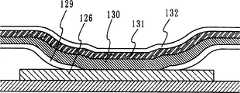
有机绝缘材料是吸湿的,吸收并吸留水分。当吸留的水分被释放时,将水分提供给发光元件309的有机化合物,这使有机发光元件劣化。为了防止水分的吸留和释放,在第二有机绝缘层128上形成厚度为10-100nm的第四无机绝缘层129。第四无机绝缘层129用包含氮化物的无机绝缘材料形成。特别地,用选自氮化硅、氮化铝和氮氧化铝的无机绝缘材料形成。形成第四无机绝缘层129以便覆盖第二有机绝缘层128的上表面和侧表面,使其和阳极层126重叠的末端锥化。Organic insulating materials are hygroscopic, absorbing and retaining moisture. When the occluded moisture is released, the moisture is supplied to the organic compound of the
用阳极层126、包含碱金属或碱土金属的阴极层131、和包含发光材料的插入有机化合物层130形成有机发光元件309。通过层叠一层或多层来形成包含发光材料的有机化合物层130。每一层根据其目的和功能进行命名,空穴注入层,空穴传输层,发光层,电子传输层和电子注入层。这些层可以用低分子量有机化合物、中分子量有机化合物、高分子量有机化合物其中之一、或者以上的其中两种化合物适当组合而形成。此外,可以形成包含电子传输材料和空穴传输材料的混合物的混合层,或者在每个界面之间形成混合区域的混合连接。The organic
阴极层131用具有较小功函数的碱金属或碱土金属形成,例如镁(Mg),锂(Li)或钙(Ca)。优选地,可以使用包含MgAg(具有10∶1比率的Mg和Ag的混合物)的电极。适合电极的其它材料包括MgAgAl,LiAl和LiFAl。也可使用碱金属或碱土金属的氟化物和低电阻金属例如铝的组合。作为公共电极的阴极层131横跨多个像素,连接到像素部分302的外部或像素部分302和驱动电路部分301之间的引线120,然后引向外部端子。图1中,在虚线包围的区域中示出了连接310。The
在那层上,第五无机绝缘层132可以用氮化硅、类金刚石碳(diamond-like-carbon)(DLC)、氮氧化铝、氧化铝或氮化铝其中之一形成。特别地,已知DLC膜具有抗氧、CO、CO2和H2O的高气体阻挡特性。希望在不将基板暴露在大气中的情况下,在形成阴极131之后接着形成第五无机绝缘层132。在第五无机绝缘层132下面设置氮化硅制成的缓冲层,以便提高粘附力。On that layer, the fifth inorganic insulating
尽管图中未示出,但可以在阳极层126和包含发光材料的有机化合物层130之间形成允许隧道电流流动的厚度0.5-5nm的第六无机绝缘层。第六无机绝缘层可防止阳极表面上任何不规则性引起的短路,可防止用于阴极等的碱金属向下层扩散。Although not shown in the drawings, a sixth inorganic insulating layer having a thickness of 0.5-5 nm allowing tunnel current to flow may be formed between the
在像素部分302上形成的第二有机绝缘层128延伸到驱动电路部分301,在形成在第二有机绝缘层128上的第四无机绝缘层129上形成密封图形133。一些或全部密封图形133和驱动电路部分301及连接驱动电路部分301和输入端子的引线117重叠,这减小了发光设备的帧区域(像素部分的周边区域)的面积。The second organic insulating
密封板134经密封图形133被固定。密封板134可以包含例如不锈钢和铝这样的金属。此外,你可以使用玻璃基板。在被密封图形133和密封板134包围的区域中可以包括例如氧化钡这样的干燥剂135,以便防止水分造成的劣化。有机树脂制成的密封板可以是柔性的,具有30-120μm的厚度。密封板的表面涂有无机绝缘材料,例如DLC和氮化硅,作为气体阻挡层。密封图形的一个示例性材料是环氧粘合剂。密封图形的侧表面可以涂有包含无机绝缘材料的膜,防止蒸气从侧表面渗透。The sealing
图1中,第一TFT305具有多栅结构,和轻掺杂的漏极(LDD)组合以减小关态电流。p-沟道型第四TFT306设有和栅电极重叠的杂质区域。In FIG. 1, the
图2示出了设有上述TFT的像素部分中的一个像素的顶视图。为了清楚地图示每个TFT的布置,在图2中未示出发光元件309、第二有机绝缘层128和第四无机绝缘层129的图形。一个像素包含第一TFT305,第二TFT311,第三TFT312,第四TFT306和电容部分307。图17示意性地示出了等价于图2所示结构的电路。图1示出了沿图2的线A-A'剖开的横截面图。图3示出了沿线B-B'剖开的横截面图。图4示出了沿图2的线C-C'剖开的横截面图。FIG. 2 shows a top view of one pixel in the pixel portion provided with the above TFT. In order to clearly illustrate the arrangement of each TFT, the patterns of the
图15示出了在像素部分中第二有机绝缘层128和第四无机绝缘层129的一个示例性结构,其中第二有机绝缘层128和第四无机绝缘层129都覆盖阳极层126的周边。在图16所示的另一个示例性结构中,第二有机绝缘层128可以仅覆盖阳极层126的两边,而第四无机绝缘层129可以覆盖阳极层126的所有边。当然,图中所示的像素结构只是一个例子,不是本发明的要求。FIG. 15 shows an exemplary structure of the second organic insulating
尽管在图1中未示出,驱动电路部分301具有用于栅极信号驱动电路和数据信号驱动电路的不同电路。引线118和119分别连接到n-沟道型TFT303和p-沟道型TFT304,这些TFT又可以用于形成移位寄存器、锁存电路或缓冲电路。Although not shown in FIG. 1 , the driving
输入端子308由和栅电极相同的层形成的引线或形成在第三无机绝缘层116上的引线形成。图1示出了由和栅电极相同的层形成的输入端子308的示例,即,由导电层109和127形成输入端子308。在形成阳极层126时,导电层127由氧化物导电材料形成。实际上,暴露到表面上的部分用氧化物导电材料覆盖,以防止由于氧化效果增大表面电阻。图7详细示出了输入端子308。图7A示出了顶视图,图7B和7C分别示出了沿线D-D'和E-E'剖开的横截面图。输入端子308用导电层109和127形成。The
如图1所示,形成第一无机绝缘层102和第二无机绝缘层114,以便夹住半导体层105和106。另一方面,有机发光元件309被第三无机绝缘层116、第五无机绝缘层132和第四无机绝缘层129包围。换言之,用无机绝缘层分别涂敷TFT和发光元件的半导体层。无机绝缘层由氮化硅或氧氮化硅膜制成,形成抗蒸气和离子杂质的阻挡层。As shown in FIG. 1 , a first inorganic insulating
污染第一TFT305和第四TFT306的如钠这样的碱金属的可能来源包括基板101和有机发光元件309。为了防止污染它们,用第一无机绝缘层102和第二无机绝缘层114包围第一TFT305和第四TFT306。由于有机发光元件309受到来自氧气和水分的严重破坏,因此用无机绝缘材料形成第三无机绝缘层116、第四无机绝缘层129和第五无机绝缘层132,以便防止受到氧气或水分的污染。此外,这些无机绝缘层用于防止有机发光元件309的碱金属元素扩散到其它部分。Possible sources of alkali metals such as sodium contaminating the
图5示出了包含图1-4中所示发光设备的组成部分的基板外形图。基板101设有像素部分302,栅极信号驱动电路301a和302b,数据信号驱动电路301c,和阴极层310的连接,输入/输出端子308和一个或一组引线117。设置密封图形133,使得一些或全部密封图形133和栅电极信号驱动电路301a和302b、数据信号驱动电路301c和将这些驱动电路部分连接到输入端子的该引线或该组引线117重叠,目的是减小发光设备的帧区域(像素部分的周边)的面积。尽管图5仅示出了一个阴极层连接310,但可以在像素部分302周围的任意位置上提供连接301,只要不干扰驱动电路部分301a-301c。Fig. 5 shows an outline view of a substrate including components of the light emitting device shown in Figs. 1-4. The
如图6所示,具有以上结构的多个基板101(101a-101d)设在母玻璃201上,在形成第四无机绝缘层、阴极层、第五无机绝缘层或密封板其中之一之后沿切割线202隔开。用金刚石切割器或激光切割器分离基板。为了使分离工序更容易,最好沿切割线202去除第三至第五无机绝缘层和第一和第二有机绝缘层。As shown in Figure 6, a plurality of substrates 101 (101a-101d) having the above structure are provided on the mother glass 201, and after forming one of the fourth inorganic insulating layer, the cathode layer, the fifth inorganic insulating layer or the sealing plate along the Cutting lines 202 are spaced apart. Separate the substrates with a diamond cutter or laser cutter. In order to make the separation process easier, it is preferable to remove the third to fifth inorganic insulating layers and the first and second organic insulating layers along the cutting line 202 .
如上所述,TFT和发光元件组合形成像素部分,完成发光设备。在如此制造的发光设备中,可利用作为像素部分的TFT在同一基板上形成驱动电路。如图1所示,通过用包含氮化硅或氧氮化硅的阻挡层和保护层包围半导体膜、栅极绝缘膜和栅电极这些TFT的主要组成部分的上表面和下表面,这种结构防止这些组成部分被碱金属和有机材料污染。有机发光元件的一部分又包含碱金属,被包含氮化硅、氧氮化硅或DLC其中之一的保护膜和包含主要由氮化硅或碳组成的绝缘膜的气体阻挡层所包围,使得该结构防止氧气和水分从外部渗透。As described above, TFTs and light emitting elements are combined to form a pixel portion, completing a light emitting device. In the light-emitting device thus produced, a driver circuit can be formed on the same substrate using TFTs as part of the pixels. As shown in FIG. 1, by surrounding the upper and lower surfaces of the main components of the TFT, the semiconductor film, the gate insulating film, and the gate electrode, with a barrier layer and a protective layer containing silicon nitride or silicon oxynitride, this structure Protect these components from contamination by alkali metals and organic materials. A part of the organic light-emitting element, in turn, contains an alkali metal, is surrounded by a protective film containing one of silicon nitride, silicon oxynitride, or DLC, and a gas barrier layer containing an insulating film mainly composed of silicon nitride or carbon, so that the The structure prevents the penetration of oxygen and moisture from the outside.
根据表1(示出了典型例子)所示的条件,在本实施例中用于无机绝缘层的包含氮化硅的膜(氮化硅膜)是通过RF溅射形成的高度精细的膜。表中的“RFSP-SiN”表示用RF溅射形成的氮化硅膜。“T/S”是靶和基板之间的距离。According to the conditions shown in Table 1 (showing a typical example), the film containing silicon nitride (silicon nitride film) used for the inorganic insulating layer in this embodiment is a highly fine film formed by RF sputtering. "RFSP-SiN" in the table indicates a silicon nitride film formed by RF sputtering. "T/S" is the distance between the target and the substrate.
表1 Table 1
RFSP-SiN加工条件
氩,作为溅射气体被引入,喷射在基板的背表面上对其加热。喷射的Ar最终和N2混合用于溅射。表1所示的用于形成膜的值仅是代表性的值,不限于这里表示的这些值。只要最后的SiN膜的物理参数落在表4(以后示出)所示的物理参数范围内,操作人员可以对这些条件进行适当修改。Argon, introduced as a sputtering gas, is sprayed on the back surface of the substrate to heat it. The sparged Ar is finally mixed withN2 for sputtering. The values for film formation shown in Table 1 are representative values only, and are not limited to those values shown here. As long as the physical parameters of the final SiN film fall within the range of physical parameters shown in Table 4 (shown later), the operator can appropriately modify these conditions.
接着,图30示出了通过上述RF溅射形成氮化硅膜所用的溅射设备的示意性视图。图30中,30是加工室壁,31是形成磁场的可移动磁铁,32是单晶硅靶,33是保护挡板,34是待加工的基板,36a和36b是加热器,37是基板夹紧设备,38是抗粘板(antitack plate),39是一个阀(导电阀或主阀)。加工室壁30设有进气管40和41,分别引入N2(或N2和惰性气体的混合气体)和惰性气体。Next, FIG. 30 shows a schematic view of a sputtering apparatus used for forming a silicon nitride film by the above-mentioned RF sputtering. In Fig. 30, 30 is a processing chamber wall, 31 is a movable magnet forming a magnetic field, 32 is a single crystal silicon target, 33 is a protective baffle, 34 is a substrate to be processed, 36a and 36b are heaters, and 37 is a substrate holder Tight device, 38 is an anti-stick plate (antitack plate), and 39 is a valve (conductive valve or main valve). The
表2示出了形成例如通过传统的等离子体CVD方法形成的氮化硅膜的条件。表中的“PCVD-SiN”指通过等离子体CVD方法形成的氮化硅膜。Table 2 shows conditions for forming a silicon nitride film formed, for example, by a conventional plasma CVD method. "PCVD-SiN" in the table refers to a silicon nitride film formed by a plasma CVD method.
表2Table 2
等离子体CVD条件
表3示出了在表1条件下和在表2条件下形成的氮化硅膜的物理特性(物理参数)的代表性值。“RFSP-SiN”(No.1)和“RFSP-SiN(No.2)之间的区别可归因于膜形成设备之间的区别,不削弱用作根据本发明的阻挡层膜的氮化硅膜的作用。内应力可以是压应力的或张应力,数值的符号相应改变,但表中仅示出了绝对值。Table 3 shows representative values of physical characteristics (physical parameters) of the silicon nitride films formed under the conditions of Table 1 and Table 2. The difference between "RFSP-SiN" (No.1) and "RFSP-SiN (No.2) can be attributed to the difference between the film forming equipment, which does not impair the nitriding of the film used as the barrier layer according to the present invention. The role of the silicon membrane. The internal stress can be compressive or tensile, and the sign of the value changes accordingly, but only the absolute value is shown in the table.
表3table 3
代表性SiN物理参数之间的比较
如表3所示,RFSP-SiN(No.1)和RFSP-SiN(No.2)中的共同特性和PCVD-SiN膜的共同特性相比,蚀刻速率(在20℃用LAL500蚀刻的蚀刻速率,同上)低,氢浓度低。“LAL500”是“LAL500 SA缓冲氟氢酸”,是NH4HF2(7.13%)和NH4F(15.4%)的溶液,由Hashimoto Kasei有限公司生产。内应力的绝对值低于用等离子CVD方法形成的氮化硅膜的绝对值。As shown in Table 3, the common characteristics of RFSP-SiN (No.1) and RFSP-SiN (No.2) are compared with the common characteristics of PCVD-SiN films, and the etching rate (etching rate at 20°C with LAL500 , same as above) low, low hydrogen concentration. "LAL500" is "LAL500 SA buffered hydrofluoric acid", a solution of NH4 HF2 (7.13%) and NH4 F (15.4%), manufactured by Hashimoto Kasei Co., Ltd. The absolute value of the internal stress is lower than that of the silicon nitride film formed by the plasma CVD method.
接着,在表4中归纳了在表1条件下由发明人形成的氮化硅膜的不同物理参数。Next, various physical parameters of the silicon nitride films formed by the inventors under the conditions of Table 1 are summarized in Table 4.
表4Table 4
本发明中使用的SiN物理参数
以上氮化硅膜的SIMS(二次离子质谱仪)和FT-IR和透射率的结果分别示于图24、25和26。图26还示出了在表2条件下形成的氮化硅膜。透射率系数几乎可和传统PCVD-SiN膜的透射率系数相比。The results of SIMS (Secondary Ion Mass Spectrometry) and FT-IR and transmittance of the above silicon nitride film are shown in Figs. 24, 25 and 26, respectively. FIG. 26 also shows the silicon nitride film formed under the conditions of Table 2. The transmittance coefficient is almost comparable to that of conventional PCVD-SiN films.
根据本发明的用作无机绝缘层的氮化硅膜最好满足表4所示的参数。即,无机绝缘层最好满足下列条件之一:(1)蚀刻速率为9nm/min或更低(最好0.5-3.5nm/min或更低)的氮化硅膜,(2)1×1021原子/cm3或更低(最好5×1020原子/cm3或更低)的氢浓度,(3)1×1021原子/cm3或更低(最好5×1020原子/cm3或更低)的氢浓度,和5×1018~5×1021原子/cm3(最好1×1019~1×1021原子/cm3)的氧浓度,和(4)蚀刻速率为9nm/min或更低(最好0.5-3.5nm/min或更低),1×1021原子/cm3或更低(最好5×1020原子/cm3或更低)的氢浓度,和(5)蚀刻速率为9nm/min或更低(最好0.5-3.5nm/min或更低),1×1021原子/cm3或更低(最好5×1020原子/cm3或更低)的氢浓度,和5×1018~5×1021原子/cm3(最好1×1019~1×1021原子/cm3)的氧浓度。The silicon nitride film used as the inorganic insulating layer according to the present invention preferably satisfies the parameters shown in Table 4. That is, the inorganic insulating layer preferably satisfies one of the following conditions: (1) a silicon nitride film with an etching rate of 9 nm/min or less (preferably 0.5-3.5 nm/min or less), (2) 1×10 A hydrogen concentration of21 atoms/cm3 or lower (preferably 5×10²⁰ atoms/cm3 or lower), (3) 1×10²¹ atoms/cm3 or lower (preferably 5×10²⁰ atoms/cm 3 cm3 or less), and an oxygen concentration of 5×10¹⁸ to 5×10²¹ atoms/cm3 (preferably 1×10¹⁹ to 1×10²¹ atoms/cm3 ), and (4) etching Hydrogen at a rate of 9 nm/min or less (preferably 0.5-3.5 nm/min or less), 1×10²¹ atoms/cm3 or less (preferably 5×10²⁰ atoms/cm3 or less) concentration, and (5) an etching rate of 9 nm/min or less (preferably 0.5-3.5 nm/min or less), 1×10²¹ atoms/cm3 or less (preferably 5×10²⁰ atoms/cm3 or less), and an oxygen concentration of 5×10¹⁸ to 5×10²¹ atoms/cm3 (preferably 1×10¹⁹ to 1×10²¹ atoms/cm3 ).
内应力的绝对值可以是2×10¹⁰dyn/cm2或更小,更好5×109dyn/cm2或更小,最好5×108dyn/cm2或更小。更小的内应力可以减小膜之间能量等级差,进一步防止由于内应力而使膜脱落。The absolute value of the internal stress may be 2 x 10¹⁰ dyn/cm2 or less, more preferably 5 x 10⁹ dyn/cm2 or less, most preferably 5 x 10⁸ dyn/cm2 or less. Smaller internal stress can reduce the energy level difference between the membranes and further prevent the membrane from falling off due to internal stress.
根据该实施例在表1所示的条件下形成的氮化硅膜具有明显阻挡周期表中属于组1和组2的元素例如Na和Li的效果,可有效抑制这些移动离子的扩散。例如,根据包括电荷注入特性等的不同物理特性,以加了0.2-1.5wt%(最好0.5-1.0wt%)锂的铝制成的金属膜用于本实施例的阴极层更可取。但是,当使用该类型的金属膜时,锂会扩散并损坏晶体管的性能。为了避免这种损坏,本实施例用无机绝缘层完全保护晶体管,使得锂不会扩散到晶体管中。The silicon nitride film formed under the conditions shown in Table 1 according to this embodiment has the effect of significantly blocking elements belonging to
这显示在图27-29中的数据中。图27是MOS结构的BT应力测试前后C-V特性的变化图,所述MOS结构具有在表2条件下形成的氮化硅膜(PCVD-SiN膜)作为电介质。样品的结构示于图29A,用Al-Li(加锂的铝)电极作为表面电极可确定锂的扩散效果。如图27所示,B-T应力测试揭露出C-V特性显著移动,这表示从表面电极扩散的锂具有本质作用。This is shown in the data in Figures 27-29. 27 is a graph showing changes in C-V characteristics before and after a BT stress test of a MOS structure having a silicon nitride film (PCVD-SiN film) formed under the conditions of Table 2 as a dielectric. The structure of the sample is shown in Fig. 29A, and the diffusion effect of lithium was determined using an Al-Li (aluminum with lithium added) electrode as the surface electrode. As shown in Figure 27, the B-T stress test revealed a significant shift in the C-V characteristics, suggesting an essential role for lithium diffusing from the surface electrodes.
图28A和28B示出了MOS结构的BT应力测试前后的C-V特性,所述MOS结构用表1条件下形成的氮化硅膜(PCVD-SiN膜)作为电介质。图28A和图28B的测试中的区别在于:在图28A的测试中用Al-Si(加硅的铝膜)电极作为表面电极,而在图28B的测试中用Al-Li(加锂的铝膜)电极作为表面电极。图28B所示的结果是图29B所示的MOS结构的测量结果。在图29B中,用热氧化膜层叠这些膜,以便减小氮化硅膜和硅基板之间的界面处能量等级差的效果。28A and 28B show the C-V characteristics before and after the BT stress test of the MOS structure using the silicon nitride film (PCVD-SiN film) formed under the conditions of Table 1 as a dielectric. The difference between the tests of Fig. 28A and Fig. 28B is that in the test of Fig. 28A an Al-Si (aluminum film with silicon added) electrode is used as the surface electrode, while in the test of Fig. 28B an Al-Li (aluminum film with lithium added membrane) electrodes as surface electrodes. The results shown in FIG. 28B are measurement results of the MOS structure shown in FIG. 29B. In FIG. 29B, these films are laminated with a thermal oxide film in order to reduce the effect of energy level difference at the interface between the silicon nitride film and the silicon substrate.
从图28A和28B中曲线可见,BT应力测试前后的C-V特性具有类似的移动图形,这表示没有锂扩散的效果,即,在表1的条件下形成的氮化硅膜有效地充当阻挡膜。As can be seen from the graphs in FIGS. 28A and 28B , the C-V characteristics before and after the BT stress test have similar moving patterns, which indicates that there is no effect of lithium diffusion, that is, the silicon nitride film formed under the conditions of Table 1 effectively acts as a barrier film.
如上所述,由于在本发明中使用的无机绝缘层非常精细且具有抗包括Na和Li的活动元素的高阻挡效果,因此可抑制从平化膜扩散脱气的成分,也有效地抑制从Al-Li电极扩散Li。利用这些效果,可实现高可靠性的显示设备。发明人认为可以将无机绝缘层作得精细,原因是硅簇(cluster)不能容易地污染膜,因为在单晶硅靶的表面上形成氮化硅薄膜,然后在基板上层叠由此制造的氮化硅膜。As described above, since the inorganic insulating layer used in the present invention is very fine and has a high blocking effect against mobile elements including Na and Li, it is possible to suppress the diffusion of degassed components from the flattened film, and it is also effective to suppress the diffusion from the Al - Li electrode diffuses Li. With these effects, a highly reliable display device can be realized. The inventors think that the inorganic insulating layer can be made fine because silicon clusters cannot easily contaminate the film because a silicon nitride film is formed on the surface of a single-crystal silicon target, and then the thus-produced nitrogen film is laminated on the substrate. Silicon film.
此外,由于通过溅射方法在相对低的温度下即室温到约200℃形成氮化硅膜,因此可以在树脂膜上形成根据本发明用作阻挡膜的氮化硅膜,这是优于等离子CVD方法的另一个优点。在通过层叠形成时,可以用以上氮化硅膜作为部分栅极绝缘膜。In addition, since the silicon nitride film is formed at a relatively low temperature, ie, room temperature to about 200° C., by the sputtering method, the silicon nitride film used as the barrier film according to the present invention can be formed on the resin film, which is superior to plasma Another advantage of the CVD method. When formed by lamination, the above silicon nitride film can be used as part of the gate insulating film.
实施例Example
实施例1Example 1
下面,参考附图说明制造图1所示的发光设备的过程。Next, a process of manufacturing the light emitting device shown in FIG. 1 will be described with reference to the accompanying drawings.
图8A中,基板101可以是玻璃基板、石英基板或陶瓷基板其中之一。基板101包括上面形成有绝缘层的硅基板,金属基板或不锈钢基板。具有可忍受实施例的加工温度的热电阻的塑料基板是可接受的。In FIG. 8A , the
由绝缘膜例如氧化硅膜、氮化硅膜或氧氮化硅膜(SiOxNy)这样的绝缘膜组成的第一无机绝缘层102形成在基板101上。典型例子具有两层结构,其中,用SiH4、NH3和N2O作为反应气体形成50nm厚的第一氧氮化硅膜,用SiH4和N2O作为反应气体形成100nm厚的第二氧氮化硅膜形成在第一膜上。A first inorganic insulating
作为活性层的半导体层可以通过结晶形成在第一无机绝缘层102上的非晶半导体膜来获得。形成的非晶半导体膜厚度为30-60nm,通过加热或照射激光束结晶。虽然在非晶半导体膜的材料上没有限制,但也可优选使用硅或硅锗(Si1-xGex;0<x<1,x的代表性值是0.001-0.05)合金。A semiconductor layer as an active layer can be obtained by crystallizing an amorphous semiconductor film formed on the first inorganic insulating
在代表性例子中,通过利用SiH4气体的等离子CVD方法形成54nm厚的非晶硅膜。为了晶化,可用掺杂Cr、Nd、Er、Ho、Ce、Co、Ti或Tm其中之一的脉冲振荡或连续振荡准分子激光器,或YAG激光器,YVO4激光器或YLF激光器。当用YAG激光器,YVO4激光器或YLF激光器其中之一时,可以使用二次谐波至四次谐波。当使用这些激光器其中之一时,从激光振荡器照射的激光束可以被光学系统线性收集,以便照射在半导体膜上。晶化的条件可以由操作人员适当进行选择。In a representative example, a 54 nm-thick amorphous silicon film was formed by a plasma CVD method using SiH4 gas. For crystallization, a pulsed or continuous oscillating excimer laser doped with one of Cr, Nd, Er, Ho, Ce, Co, Ti or Tm, or a YAG laser, YVO4 laser or YLF laser can be used. When using one of the YAG laser, YVO4 laser or YLF laser, the second harmonic to the fourth harmonic can be used. When one of these lasers is used, a laser beam irradiated from a laser oscillator can be linearly collected by an optical system to be irradiated on a semiconductor film. Conditions for crystallization can be appropriately selected by the operator.
在晶化中,可添加某种金属元素,例如可用作半导体结晶的催化剂的镍。结晶的一个示例性过程是:将包含镍的溶液保持在非晶硅膜上,脱氢(500℃,一个小时),热结晶(550℃,四个小时),然后照射选自YAG激光器,YVO4激光器或YLF激光器的连续振荡激光器的二次谐波,以便改善结晶。In the crystallization, a certain metal element such as nickel which can be used as a catalyst for semiconductor crystallization may be added. An exemplary process of crystallization is: keeping a solution containing nickel on an amorphous silicon film, dehydrogenation (500°C, one hour), thermal crystallization (550°C, four hours), and then irradiating a laser selected from YAG, YVO4 lasers or the second harmonic of continuous oscillation lasers of YLF lasers for improved crystallization.
通过光刻法以期望的形式蚀刻最后得到的结晶半导体膜,所述光刻法用光掩模(1)形成象岛一样隔开的半导体层103-107。图12示出了这时像素的顶视图。The resulting crystalline semiconductor film is etched in a desired form by photolithography, which uses a photomask (1) to form semiconductor layers 103-107 separated like islands. Figure 12 shows a top view of the pixel at this time.
此外,在非晶半导体膜结晶之后,为了控制TFT的阈值,可以用p-型杂质元素掺杂膜。p-型杂质元素包括属于周期表中族13的元素,例如硼(B),铝(Al)和镓(Ga)。In addition, after crystallization of the amorphous semiconductor film, in order to control the threshold value of TFT, the film may be doped with a p-type impurity element. The p-type impurity elements include elements belonging to
下面,如图8B所示,形成覆盖象岛一样隔开的半导体层103-107的栅极绝缘膜108。利用氧化硅或氧氮化硅这样的无机绝缘材料,通过等离子CVD方法或溅射形成40-150nm厚的栅极绝缘膜108。该栅极绝缘层可以用包含硅的绝缘膜作为单层结构或层叠结构。Next, as shown in FIG. 8B, a
包含氮化钽(TaN)的10-50nm厚的第一导电膜10和包含钨(W)的100-400nm厚的第二导电膜11层叠在栅极绝缘膜108上,目的是形成栅电极。用于栅电极的其它导电材料可以选自Ta、W、Ti、Mo、Al、Cu或用以上元素其中之一作为主要成分的合金或化学化合物。此外,可以使用包括掺杂了杂质元素例如磷的多晶硅膜的半导体膜。而且,也可以施加:第一导电膜钽膜(Ta)和第二导电膜W膜的组合,第一导电膜氮化钽(TaN)膜和第二导电膜Al膜的组合,或者第一导电膜氮化钽(TaN)膜和第二导电膜Cu膜的组合。A 10-50 nm thick first
下面,如图8C所示,由形成栅电极图形的掩模12使用光掩模(2)通过光刻法来形成。此后,用干腐蚀例如ICP(感应耦合等离子体)腐蚀来完成第一蚀刻。虽然对蚀刻气体没有限制,但可以用CF4、Cl2和O2进行W和TaN的蚀刻。在第一蚀刻中,向基板施加预定的偏压,在形成的电极图形13-17的侧表面上产生15-50度的倾斜角。第一蚀刻易于同时蚀刻该绝缘膜上的暴露区域,形成比另一个区域薄10-30nm的区域。Next, as shown in FIG. 8C, a
下面,将条件改变到第二蚀刻条件,用SF6、Cl2和O2作为蚀刻气体在W膜上执行各向异性蚀刻,并向基板施加预定偏压。由此形成栅电极110-113和输入端子的引线109。此后,去除掩模12。第二蚀刻易于同时蚀刻该绝缘膜上的暴露区域,形成比另一个区域薄10-30nm的区域。图13示出了的在这一点处像素部分的顶视图。Next, the conditions were changed to the second etching conditions, anisotropic etching was performed on the W film using SF6 , Cl2 , and O2 as etching gases, and a predetermined bias voltage was applied to the substrate. Thus, the gate electrodes 110-113 and the
在形成栅电极之后,如图9A所示执行第一次掺杂,以在半导体层中形成第一n-型杂质区域18-22。这些第一n-型杂质区域用栅电极作掩模以自对准方式形成。可以适当设定掺杂条件,用氢稀释的5%PH3,以50kV注入6×10¹³/cm2剂量。After forming the gate electrode, first doping is performed as shown in FIG. 9A to form first n-type impurity regions 18-22 in the semiconductor layer. These first n-type impurity regions are formed in a self-alignment manner using the gate electrode as a mask. The doping conditions can be properly set, and a dose of 6×10¹³ /cm2 is implanted at 50 kV with 5% PH3 diluted with hydrogen.
接着,如图9B所示,利用光掩模(3)通过光刻法形成掩模23,完成第二次掺杂。第二掺杂使用用氢稀释的5%PH3,以65kV注入3×10¹⁵原子/cm2剂量,形成第二n-型杂质区域24、25和第三n-型杂质区域26。在半导体层103中,用栅电极作为掩模以自对准方式,在栅电极的外面形成第二n-型杂质区域24,在和栅电极重叠的位置上形成第三n-型杂质区域26。第二n-型杂质区域25通过掩模23形成在半导体层105中。Next, as shown in FIG. 9B , a
接着,如图9C所示,利用光掩模(4)通过光刻法形成掩模27,完成第三次掺杂。第三掺杂使用用氢稀释的5%PH3,以80kV注入2×10¹⁶原子/cm2剂量,在半导体层104、106和107中形成p-型杂质区域28-30。Next, as shown in FIG. 9C , a mask 27 is formed by photolithography using the photomask ( 4 ), and the third doping is completed. The third doping uses 5% PH3 diluted with hydrogen at a dose of 2×10¹⁶ atoms/cm2 implanted at 80 kV to form p-type impurity regions 28 - 30 in
作为以上过程的结果,在每个半导体层中分别形成具有n-型导电性或p-型导电性的杂质区域。如图10A所示,在半导体层103中,第二n-型杂质区域24充当源极或漏极区域,第三n-型杂质区域26充当LDD区域。在半导体层104中,p-型杂质区域28充当源极或漏极区域。在半导体层105中,第二n-型杂质区域25充当源极或漏极区域,第一n-型杂质区域20充当LDD区域。在半导体层106中,p-型杂质区域29充当源极或漏极区域。As a result of the above process, impurity regions having n-type conductivity or p-type conductivity are formed in each semiconductor layer, respectively. As shown in FIG. 10A, in the
接着,形成几乎覆盖整个表面的第二无机绝缘层114。利用等离子CVD或溅射,用包含硅或氢的无机绝缘材料形成厚100-200nm的第二无机绝缘层114。最佳例子是通过利用SiH4、N2O、NH3和H2的等离子CVD形成的厚100nm的氧氮化硅膜。此后,在氮气氛中以410℃加热1小时。该加热过程的目的是氢化氧氮化硅膜,以便使其成为氢的来源。Next, the second inorganic insulating
接着,如图10B所示,在第二无机绝缘层114上形成0.5-1μm的第一有机绝缘层115。可以用热固性聚丙烯材料作为有机绝缘材料,它是被旋涂的,在250℃下煅烧,形成平化膜。在该膜上,形成50-100nm厚的第三无机绝缘层116。Next, as shown in FIG. 10B , the first organic insulating
当形成第三无机绝缘层116时,在80-200℃下加热具有上面形成有第二无机绝缘层114的基板来脱水。适于第三无机绝缘层116的一个示例性材料是用硅作为靶通过溅射形成的氮化硅膜。可以适当选择形成膜的条件。最好是,通过用于溅射的RF功率施加氮(N2)或氮和氩的混合物。可以在从室温到200℃的温度范围内对基板进行处理。When the third inorganic insulating
接着,如图10C所示,使用光掩模(5)通过光刻法形成掩模图形,通过干腐蚀形成输入端子的接触孔30和开口31。干腐蚀的条件如下:用CF4、O2和He蚀刻第三无机绝缘层116和第一有机绝缘层115,然后,用CHF3蚀刻第二无机绝缘层和栅电极绝缘层。Next, as shown in FIG. 10C, a mask pattern is formed by photolithography using a photomask (5), and contact holes 30 and
此后,如图11A所示,用Al、Ti、Mo或W形成引线和像素电极。用光掩模(6)形成引线。例如,使用厚50-250nm的Ti膜和厚300-500nm的Al和Ti的合金膜的层叠膜。由此形成引线117-125。接着,通过溅射形成厚30-120nm的ITO,然后使用光掩模(7)通过光刻法在其上形成预定图形。由此形成发光元件的阳极层126,在输入端子的引线上形成ITO膜127。图14示出了在该阶段的像素的顶视图。Thereafter, as shown in FIG. 11A, Al, Ti, Mo, or W are used to form wirings and pixel electrodes. Leads are formed using a photomask (6). For example, a laminated film of a Ti film having a thickness of 50 to 250 nm and an alloy film of Al and Ti having a thickness of 300 to 500 nm is used. Leads 117-125 are thus formed. Next, ITO is formed to a thickness of 30-120 nm by sputtering, and then a predetermined pattern is formed thereon by photolithography using a photomask (7). In this way, the
接着,如图11B所示,形成第二有机绝缘层128。该层用类似于第一有机绝缘层115的聚丙烯材料形成。之后,在阳极层126、阴极层310的连接和输入端子上使用光掩模(8)形成开口。形成第二有机绝缘层128,以便覆盖阳极126的末端,其侧表面具有40度的倾斜角。Next, as shown in FIG. 11B , a second organic insulating
有机绝缘层材料是吸湿的且吸留水分。为了防止水分的吸留和释放,在第二有机绝缘层128上形成厚10-100nm的第四无机绝缘层129。第四无机绝缘层129用含氮化物的无机绝缘材料形成。第四无机绝缘层129由通过溅射制造的氮化硅膜形成。可用膜类似于用于第三无机绝缘层116的膜。第四无机绝缘层129覆盖第二有机绝缘层128的上表面和侧表面,锥形末端和阳极层126重叠。这样,在输入端子处形成第四无机绝缘层129,以便覆盖第二有机绝缘层128上形成的开口的侧表面,从而防止水分进入该区域。Organic insulating layer materials are hygroscopic and absorb moisture. In order to prevent occlusion and release of moisture, a fourth inorganic insulating
接着,形成包含发光材料的有机化合物层130。通过溅射或电阻加热淀积在包含发光材料的有机化合物层上形成阴极层131。用氟化钙或氟化铯作为阴极材料并通过真空淀积对其进行淀积来形成阴极层131。Next, an
阴极131由氟化锂和铝的层叠结构形成。用惰性气体(通常为氩)作为溅射气体。溅射气体的离子不仅被外层覆盖物电场加速且和靶不一致,而且被弱外层覆盖物电场加速并在阳极下注入包含发光材料的有机化合物层130中。惰性气体通过位于有机化合物层晶格之间而防止分子或原子移位,改善了有机化合物的稳定性。此外,形成在阳极131上的第五无机绝缘层132由氮化硅或DLC膜形成。惰性气体的离子(通常是氩)在基板的侧面上被弱外层覆盖物电场加速并穿过阳极在阳极131下注入到有机化合物层131中。然后,可得到改善有机化合物的稳定性的效果。The
最后,形成密封图形,粘接密封板,制造图1所示的发光设备。Finally, the sealing pattern is formed, the sealing plate is bonded, and the light emitting device shown in FIG. 1 is manufactured.
实施例2Example 2
本实施例和实施例1的不同结构在于像素部分,如图31和32所示。在该实施例中,从开始到形成第三无机绝缘层116引线123、阳极126的过程和图1相同。The difference between this embodiment and
如图31A所示,覆盖阳极126末端的第二有机绝缘层180由感光负型丙烯酸树脂形成。这样,第二有机绝缘层180和阳极126接触的末端具有图中所示的有曲率的倾斜表面,其形状可以用至少两个曲率R1和R2表达。R1的中心位于引线上,而R2的中心位于引线下方。该形状可根据曝光度轻微变化,膜的厚度是1.5μm,R1和R2的值是0.2-2μm。该倾斜的表面具有连续变化的曲率。As shown in FIG. 31A, the second organic insulating
接着,沿具有这些平滑曲率的倾斜表面,形成如图31B所示的第四无机绝缘层129、有机化合物层130、阴极层131和第五无机绝缘层132。第二有机绝缘层180的该部分的形状具有减轻应力的效果(特别地,阳极126、第四无机绝缘层129和有机化合物层130重叠的区域),可防止发光元件从该末端部分劣化。即,这种结构可防止从像素周边开始然后扩展到其它区域的连续劣化。换言之,不能扩大不发光的区域。Next, along the inclined surface having these smooth curvatures, a fourth inorganic insulating
图32A示出了一个例子,其中,第二有机绝缘层181用感光正性丙烯酸树脂来代替感光负性丙烯酸树脂来形成。在这种情况下,末端部分的形状是不同的。R3的曲率半径是0.2-2,其中心位于阳极层126下方。在形成第二有机绝缘层181之后,沿具有图32B所示曲率的倾斜表面形成第四无机绝缘层129、有机化合物层130、阴极层131和第五无机绝缘层132。通过该结构可获得类似的效果。FIG. 32A shows an example in which the second organic insulating layer 181 is formed using a photosensitive positive acrylic resin instead of a photosensitive negative acrylic resin. In this case, the shape of the end portion is different. The radius of curvature of R3 is 0.2-2, and its center is located below the
该实施例可以和实施例1和2组合起来实施。This embodiment can be implemented in combination with
实施例3Example 3
对于实施例1-2,对发光元件309中有机化合物层的结构不限制,以便可使用任何已知的结构。有机化合物层130具有发光层,空穴注入层,电子注入层,空穴传输层和电子传输层,可以具有层叠这些层的结构,或形成这些层的部分或全部材料混合的结构。特别地,包括发光层,空穴注入层,电子注入层,空穴传输层和电子传输层。基板EL元件具有按阳极、发光层、阴极这种顺序层叠的结构。其它可能的结构包括按阳极、空穴注入层、发光层和阴极这样顺序层叠层的结构,或者按阳极、空穴注入层、发光层、电子传输层和阴极这种顺序层叠层的结构。For Embodiment 1-2, the structure of the organic compound layer in the
典型地,用有机化合物形成发光层。但是,也可以用包括有机化合物或无机化合物和发光材料的电荷注入传输材料形成,它可包含选自低分子有机化合物、中分子有机化合物和聚合有机化合物的有机化合物制成的一个或多个层,发光层可以和电子注入传输型或空穴注入传输型的无机化合物组合。中分子有机化合物指不升华的且分子数位为20或更少,或者链接分子的长度不超过10μm的有机化合物。Typically, organic compounds are used to form the light emitting layer. However, it may also be formed with a charge injection transport material including an organic compound or an inorganic compound and a luminescent material, which may include one or more layers made of an organic compound selected from a low-molecular organic compound, a middle-molecular organic compound, and a polymeric organic compound , the light emitting layer may be combined with an electron injection transport type or a hole injection transport type inorganic compound. Medium-molecular organic compounds refer to organic compounds that are non-sublimable and have a molecular number of 20 or less, or linking molecules whose length does not exceed 10 μm.
可用的发光材料包括络合物,例如三-8-喹啉铝(tris-8-quinolinolatoalumium)络合物或双(苯并喹啉(benzoquinolinolato))铍络合物作为低分子有机化合物,苯基蒽衍生物,四芳基二胺衍生物和联苯乙烯苯衍生物。用以上材料其中之一作为主物质,可以施加香豆素衍生物,DCM,喹吖啶酮和红荧烯。也可以施加其它已知的材料。聚合有机化合物包括聚对亚苯基1,2-亚乙烯基(polyparaphenylenevinylenes),聚对亚苯基(polyparaphenylens),聚噻吩和聚芴,包括聚(p-亚苯基1,2亚乙烯基):(PPV),聚(2,5-二烷氧基-1,4-亚苯基1,2亚乙烯基):(RO-PPV),聚[2-2'-乙基己氧基(ethylhexoxy)]-5-甲氧基-1,4-亚苯基1,2亚乙烯基]:(MEH-PPV),聚[2-(二烷氧基苯)-1,4-亚苯基1,2亚乙烯基]:(ROPh-PPV),聚(p-亚苯基):(PPP),聚(2,5-二烷氧基-1,4-亚苯基):(RO-PPP),聚(2,5-二己氧基(dihexoxy)-1,4-亚苯基),聚噻吩:(PT),聚(3-烷基噻吩):(PAT),聚(3-己基噻吩):(PHT),聚(3-环己基噻吩):(PCHT),聚(3-环己基-4-甲基噻吩):(PCHMT),聚(3,4-二环己基噻吩);(PDCHT),聚[3-(4-辛基苯)-噻吩]:(POPT),聚[3-(4-辛基苯)-2,2-并噻吩]):(PTOPT),聚芴:(PF),聚(9,9-二烷基芴):(PDAF),聚(9,9-二辛基芴):(PDOF)。Usable luminescent materials include complexes such as tris-8-quinolinolatoalumium complex or bis(benzoquinolinolato)beryllium complex as low-molecular organic compounds, phenyl Anthracene derivatives, tetraaryldiamine derivatives and distyrylbenzene derivatives. Using one of the above materials as the main substance, coumarin derivatives, DCM, quinacridone and rubrene can be applied. Other known materials may also be applied. Polymeric organic compounds include polyparaphenylenevinylenes, polyparaphenylens, polythiophenes, and polyfluorenes, including poly(p-phenylenevinylenes) : (PPV), poly(2,5-dialkoxy-1,4-phenylene 1,2 vinylene): (RO-PPV), poly[2-2'-ethylhexyloxy ( ethylhexoxy)]-5-methoxy-1,4-phenylene 1,2-vinylene]: (MEH-PPV), poly[2-(dialkoxybenzene)-1,4-phenylene 1,2 vinylene]: (ROPh-PPV), poly(p-phenylene): (PPP), poly(2,5-dialkoxy-1,4-phenylene): (RO- PPP), poly(2,5-dihexoxy (dihexoxy)-1,4-phenylene), polythiophene: (PT), poly(3-alkylthiophene): (PAT), poly(3- Hexylthiophene): (PHT), poly(3-cyclohexylthiophene): (PCHT), poly(3-cyclohexyl-4-methylthiophene): (PCHMT), poly(3,4-dicyclohexylthiophene) ; (PDCHT), poly[3-(4-octylphenyl)-thiophene]: (POPT), poly[3-(4-octylphenyl)-2,2-thiophene]): (PTOPT), poly Fluorene: (PF), poly(9,9-dialkylfluorene): (PDAF), poly(9,9-dioctylfluorene): (PDOF).
电荷注入传输层可使用无机化合物,例如类金刚石碳(DLC)、Si、Ge和其氧化物和氮化物。以上材料还可以适当添加P、B或N。此外,电荷注入传输层可以是碱金属或碱土金属的氧化物、氮化物或氟化物,或者至少有Zn、Sn、V、Ru、Sm和In的碱金属或碱土金属的化合物或合金。The charge injection transport layer can use inorganic compounds such as diamond-like carbon (DLC), Si, Ge, and oxides and nitrides thereof. The above materials can also be appropriately added with P, B or N. In addition, the charge injection transport layer may be an oxide, nitride or fluoride of an alkali metal or an alkaline earth metal, or a compound or alloy of an alkali metal or an alkaline earth metal containing at least Zn, Sn, V, Ru, Sm, and In.
列出的材料只是例子。利用这些材料,可以制造功能层,例如空穴注入传输层,空穴传输层,电子注入传输层,电子传输层,发光层,电子阻挡层和空穴阻挡层,将它们适当层叠,形成发光元件。此外,还可形成将这些层组合起来的混合层或混合连接。电致发光具有两种类型的光,即:在从单重激发态移回到基态时发射的光(荧光),和从三重激发态移回到基态时发射的光(磷光)。根据本发明的电致发光元件可以使用其中一种光或两种光都使用。The materials listed are examples only. Using these materials, it is possible to manufacture functional layers such as hole injection transport layer, hole transport layer, electron injection transport layer, electron transport layer, light emitting layer, electron blocking layer and hole blocking layer, and stack them appropriately to form a light emitting element . Furthermore, hybrid layers or hybrid connections combining these layers can also be formed. Electroluminescence has two types of light, namely: light emitted when moving from a singlet excited state back to a ground state (fluorescence), and light emitted when moving from a triplet excited state back to a ground state (phosphorescence). The electroluminescence element according to the present invention can be used with either light or with both lights.
本实施例可以和实施例1-3组合起来实施。This embodiment can be implemented in combination with Embodiments 1-3.
实施例4Example 4
可以将实施例1中发光元件309的阳极层126和阴极层131颠倒。在这种情况下,按阳极层126、有机化合物层130和阴极层131的顺序层叠层。代替ITO,也可以将具有半透明性、厚度为10-30nm的功函数为4eV或更大的金属氮化物(例如氮化钛)用于阴极层126。此外,可以在厚10-30nm的铝层上形成有厚0.5-5nm的氟化锂形成的阴极层131。The
本实施例可以和实施例1-4组合起来进行实施。This embodiment can be implemented in combination with Embodiments 1-4.
实施例5Example 5
参考附图18描述本实施例中施加到TFT上的半导体层的制造过程实施例。在本实施例中,连续振荡激光束扫描形成在绝缘表面上的非晶硅膜,从而使其结晶。An example of the manufacturing process of the semiconductor layer applied to the TFT in this example will be described with reference to FIG. 18 . In this embodiment, a continuous oscillating laser beam scans an amorphous silicon film formed on an insulating surface, thereby crystallizing it.
如图18A所示,包含厚度100nm的氧氮化硅膜的阻挡层402形成在玻璃基板401上。在阻挡层402上,通过等离子CVD方法形成厚54nm的非晶硅膜403。As shown in FIG. 18A , a barrier layer 402 including a silicon oxynitride film with a thickness of 100 nm is formed on a glass substrate 401 . On the barrier layer 402, an amorphous silicon film 403 was formed to a thickness of 54 nm by the plasma CVD method.
激光束是通过Nd:YVO4激光振荡器连续振荡照射的连续光束,照射通过波长转换元件所得到的二次谐波(532nm)。通过光学系统以椭圆形收集连续的振荡激光束,并且通过将基板401的相对位置移到激光照射光束405的点上,使非晶硅膜403结晶,形成晶体硅膜404。可以采用F20圆柱形透镜作为光学系统,在照射的表面上将直径2.5mm的激光束变换成长轴2.5mm、短轴20μm的椭圆形形状。The laser beam is a continuous beam irradiated with continuous oscillation by a Nd:YVO4 laser oscillator, and irradiated with a second harmonic (532 nm) obtained by a wavelength conversion element. A continuous oscillating laser beam is collected in an ellipse by an optical system, and by shifting the relative position of the substrate 401 to the point of the laser irradiation beam 405, the amorphous silicon film 403 is crystallized to form a crystalline silicon film 404. An F20 cylindrical lens can be used as an optical system to transform a laser beam with a diameter of 2.5 mm into an elliptical shape with a major axis of 2.5 mm and a minor axis of 20 μm on the irradiated surface.
当然,同样可使用其它激光振荡器。作为连续固态激光振荡器,可使用用晶体的激光振荡器,晶体例如YAG、YVO4、YLF或YALO3,掺杂Cr、Nd、Er、Ho、Ce、Co、Ti或Tm。Of course, other laser oscillators can be used as well. As a continuous solid-state laser oscillator, a laser oscillator using a crystal such as YAG, YVO4 , YLF or YALO3 doped with Cr, Nd, Er, Ho, Ce, Co, Ti or Tm can be used.
当用Nd:YVO4激光振荡器的二次谐波(532nm)时,通过玻璃基板401和阻挡层402发射该波长的激光束。所以,如图18B所示,可以从玻璃基板401侧照射激光束406。When the second harmonic (532 nm) of the Nd:YVO4 laser oscillator is used, a laser beam of this wavelength is emitted through the glass substrate 401 and the blocking layer 402 . Therefore, as shown in FIG. 18B, the laser beam 406 can be irradiated from the glass substrate 401 side.
结晶从照射激光束405的区域开始,形成晶体硅膜404。可以在向前或向后的一个方向上扫描激光束。当向后和向前扫描时,每次扫描可以改变激光能量密度,以便逐渐结晶。扫描也可以有脱氢作用,这在非晶硅膜将被结晶时通常是必要的。在那种情况下,可以以更低的能量密度执行第一次扫描,接着,在脱氢之后,以较高的能量密度执行第二次扫描,从而完成结晶。这种过程也可提供结晶半导体膜,在该膜中,晶粒在激光束扫描的方向上延伸。在这些工序之后,将半导体层向岛一样分隔,这可用于实施例1。Crystallization starts from a region where the laser beam 405 is irradiated, and a crystalline silicon film 404 is formed. The laser beam can be scanned in one direction, forward or backward. When scanning backwards and forwards, each scan can change the laser energy density for gradual crystallization. Scanning can also have a dehydrogenation effect, which is usually necessary when amorphous silicon films are to be crystallized. In that case, a first scan may be performed at a lower energy density, followed by a second scan at a higher energy density after dehydrogenation to complete the crystallization. This process can also provide a crystalline semiconductor film in which crystal grains extend in the direction in which the laser beam is scanned. After these processes, the semiconductor layer is divided like islands, which can be used in
该实施例所示的结构仅是示例性的。只要能获得类似的效果,也可使用其它的激光振荡器、其它的光学系统及其组合。The structure shown in this embodiment is only exemplary. Other laser oscillators, other optical systems, and combinations thereof may also be used as long as similar effects can be obtained.
实施例6Example 6
下面参考图19说明应用到实施例1中的TFT上的半导体层制造过程的一个实施例。在该实施例中,事先晶化形成在绝缘表面上的非晶硅膜,然后,通过连续振荡的激光束来扩展晶粒的尺寸。An embodiment of the manufacturing process of the semiconductor layer applied to the TFT in
如图19A所示,如实施例1那样,在玻璃基板501上形成阻挡层502和非晶硅膜503。为了将Ni作为金属元素加到较低的结晶温度并促进晶化,旋涂乙酸镍5ppm溶液,形成包含层504的催化剂元素。As shown in FIG. 19A , as in Example 1, a barrier layer 502 and an amorphous silicon film 503 are formed on a glass substrate 501 . In order to add Ni as a metal element to a lower crystallization temperature and promote crystallization, a 5 ppm solution of nickel acetate was spin-coated to form a catalyst element containing layer 504 .
如图19B所示,通过在580℃加热四个小时晶化非晶硅膜。通过Ni的作用,在非晶硅膜中形成并扩散硅化物,同时晶体生长。最后得到的晶体硅膜506由条形或针形晶体组成,从宏观角度看时,每个晶体在特定方向上生长,这样,结晶方向是均一的。并且,其特征在于平面(110)具有高取向率。As shown in Fig. 19B, the amorphous silicon film was crystallized by heating at 580°C for four hours. By the action of Ni, silicide is formed and diffused in the amorphous silicon film while crystals grow. The finally obtained crystalline silicon film 506 is composed of strip-shaped or needle-shaped crystals, and each crystal grows in a specific direction when viewed from a macroscopic point of view, so that the crystallization direction is uniform. And, it is characterized in that the plane (110) has a high orientation rate.
如图19C所示,通过连续振荡激光束508执行扫描,从而提高晶体硅膜506的结晶质量。通过照射激光束,晶体硅膜熔化并再结晶。在该再结晶中,晶粒在激光束的扫描方向上延伸。由于晶体硅膜的表面是均匀的,因此能抑制具有不同结晶平面的晶粒的淀积和错位的形成。在这些工序之后,半导体象岛一样被分离,这可适用于实施例1。As shown in FIG. 19C, scanning is performed by continuously oscillating the laser beam 508, thereby improving the crystalline quality of the crystalline silicon film 506. By irradiating a laser beam, the crystalline silicon film is melted and recrystallized. In this recrystallization, crystal grains extend in the scanning direction of the laser beam. Since the surface of the crystalline silicon film is uniform, deposition of crystal grains having different crystal planes and formation of dislocations can be suppressed. After these processes, the semiconductor is separated like islands, which is applicable to
实施例7Example 7
下面参考图20说明实施例1中施加到TFT上的半导体层的制造过程的实施例。An example of the manufacturing process of the semiconductor layer applied to the TFT in Example 1 will be described below with reference to FIG. 20 .
如图20A所示,如实施例1那样,在玻璃基板511上形成阻挡层512和非晶硅膜513。在该膜上,由等离子CVD形成厚100nm的氧化硅膜作为掩模绝缘膜514,并设置开口515。为了作为催化剂元素添加Ni,旋涂乙酸镍5ppm溶液。Ni溶液在开口515处和非晶硅膜接触。As shown in FIG. 20A , as in Example 1, a
下面,如图20B所示,通过在580℃加热四个小时晶化非晶硅膜。通过催化剂元素的作用,晶体从平行于基板表面的方向上的开口515开始生长。最后得到的晶体硅膜517由条形或针形晶体组成,从宏观角度看时,每个晶体在特定方向上生长,这样,结晶方向是均一的。并且,它在特定方向上取向。Next, as shown in Fig. 20B, the amorphous silicon film is crystallized by heating at 580°C for four hours. Crystals grow from the
加热后,通过蚀刻去除掩模绝缘膜514,获得图20C所示的晶体硅膜517。在这些工序之后,半导体层象岛一样被分离,这可适用于实施例1。After heating, the
实施例8Example 8
在实施例6或7中,在形成晶体硅膜507或517之后,可增加一道工序,通过吸杂法去除留在浓度为1019原子/cm3或更高的膜中的催化剂元素。In Embodiment 6 or 7, after forming the
如图21所示,在晶体硅膜507上形成包含氧化硅薄膜的阻挡层509,然后,通过溅射形成加有1×10²⁰原子/cm3-1×1021原子/cm3氩或磷的非晶硅膜,作为吸杂位置510。As shown in FIG. 21, a barrier layer 509 including a silicon oxide film is formed on a crystalline silicon film 507, and then, argon or phosphorous doped with 1×10²⁰ atoms/cm3 to 1×10²¹ atoms/cm3 is formed by sputtering. The amorphous silicon film serves as the gettering site 510 .
通过以炉内退火在600℃下加热12小时,或者以用灯光或加热气体的RTA在650-800℃下加热30-60分钟,作为催化剂元素添加的Ni可被分离到吸杂位置510。该过程将晶体硅膜507的催化剂元素浓度降低到1017原子/cm3或更小。Ni added as a catalyst element can be isolated to gettering sites 510 by heating at 600° C. for 12 hours with furnace annealing, or at 650-800° C. for 30-60 minutes with RTA with light or heating gas. This process reduces the catalyst element concentration of the crystalline silicon film 507 to 1017 atoms/cm3 or less.
在类似条件下进行吸杂对在实施例5中形成的晶体硅膜是有效的。通过这种吸杂,可以去除包含在晶体硅膜中的少量金属元素,所述晶体硅膜是通过向非晶硅膜照射激光束形成的。Gettering under similar conditions was effective for the crystalline silicon film formed in Example 5. By this gettering, a small amount of metal elements contained in a crystalline silicon film formed by irradiating a laser beam to an amorphous silicon film can be removed.
实施例9Example 9
图23示出了由EL面板制成模块的实施例,如实施例1所示,在所述面板中,在玻璃基板上整体形成像素部分和驱动电路部分。图23A示出了一个EL模块,在模块上,例如包含电源电路的IC安装在EL面板上。Fig. 23 shows an example in which a module is made of an EL panel in which a pixel portion and a driving circuit portion are integrally formed on a glass substrate as shown in
在图23A中,EL面板800设有:像素部分803,具有用于每个像素的发光元件;扫描线驱动电路804,用于选择像素部分803中的像素;信号线驱动电路805,用于向所选像素提供视频信号。此外,印刷基板806设有控制器801和电源电路802。从控制器801或电源电路802输出的各种信号和电源电压经FPC807提供给EL面板800的像素部分803、扫描线驱动电路804和信号线驱动电路805。In FIG. 23A, an
电源电压和各种信号经布置多个输入端子的接口(I/F)部分808提供给印刷基板806。在该实施例中,用FPC在EL面板800上安装印刷基板806,但本发明不限于这种特殊结构。用COG(玻璃上芯片)技术可以在EL面板800上直接安装控制器801和电源电路802。在印刷基板806中,由于可防止信号尖锐上升沿的在布线中形成的电容或布线本身的电阻会在电源电压或信号中引入噪声。为了避免这个问题,印刷基板806可设有电容器或缓冲器这样的元件,以便防止电源电压或信号上的噪声,并保持尖锐的信号上升沿。A power supply voltage and various signals are supplied to the printed substrate 806 via an interface (I/F)
图23B是印刷基板806的结构方框图。提供给接口808的各种信号和电源电压被提供给控制器801和电源电路802。控制器801具有A/D转换器809、PLL(锁相回路)810、控制信号发生器811和SRAM(静态随机存取存储器)812和813。尽管本实施例用SRAM,但也可以使用SDRAM或DRAM(动态随机存取存储器,只要能高速读/写数据)。FIG. 23B is a block diagram showing the structure of the printed substrate 806 . Various signals and power supply voltages supplied to the
经接口808提供的视频信号通过A/D转换器809从并行形式转换为串行形式,然后作为对应于R、G、B色的视频信号分别输入到控制信号发生器811中。基于经接口808提供的信号,A/D转换器809产生Hsync信号、Vsync信号,时钟信号CLK,交流电压[VAC],所有这些都输入到控制信号发生器811中。Video signals supplied via the
锁相回路810能使经接口808提供的各种信号的频率段和控制信号发生器811的工作频率匹配。控制信号发生器811的工作频率不总和经接口808提供的各种信号的频率相同,使得锁相回路810调整控制信号发生器811的工作频率,从而使该频率和信号的频率同步。输入到控制信号发生器811中的视频信号临时写入并存储在SRAM812和813中。控制信号发生器811从存储在SRAM812中的所有视频信号位中一次一位地读出对应于所有像素的视频信号,并将该位提供给EL面板800的信号线驱动电路805。The phase-locked
控制信号发生器811将与发光元件为每个位发射光期间相关的信息提供给EL面板800的扫描线驱动电路804。电源电路802将预定的电源电压提供给EL面板800的信号线驱动电路805、扫描线驱动电路804和像素部分803。The
图22示出了电子设备的例子,其中可包含以上EL模块。Fig. 22 shows an example of electronic equipment in which the above EL module can be incorporated.
图22A是包含上述EL模块的电视接收机的例子,包含外壳3001,支座3002和显示单元3003。在显示单元3003中采纳根据本发明制造的TFT基板,完成电视接收机。FIG. 22A is an example of a television receiver including the above-mentioned EL module, including a
图22B是包含EL模块的视频摄像机的一个例子,包含机体3011、显示单元3012、声音输入3013、操作开关3014、电池3015和图像接收部分3016。在显示单元3012中采纳根据本发明制造的TFT基板,完成视频摄像机。22B is an example of a video camera including an EL module, including a
图22C是包含EL模块的笔记本型个人计算机的一个例子,包含机体3021、外壳3022、显示单元3023和键盘3024。在显示单元3023中采纳根据本发明制造的TFT基板,完成个人计算机。FIG. 22C is an example of a notebook-type personal computer including an EL module, and includes a
图22D是包含EL模块的PDA(个人数字助理)的例子,包含机体3031、输入笔3032、显示单元3033、操作按钮3034和外部接口3035。在显示单元3033中采纳根据本发明制造的TFT基板,完成PDA。22D is an example of a PDA (Personal Digital Assistant) including an EL module, including a
图22E是包含EL模块的汽车音响系统的例子,包含机体3041、显示单元3042、操作开关3043和3044。在显示单元3042中采纳根据本发明制造的TFT基板,完成汽车音响系统。FIG. 22E is an example of a car audio system including an EL module, including a
图22F是包含EL模块的数字照相机的一个例子,包含机体3051、显示单元(A)3052、目镜3053、操作开关3054、显示单元(B)3055和电池3056。在显示单元(A)3052和(B)3055中采纳根据本发明制造的TFT基板,完成数字照相机。22F is an example of a digital camera including an EL module, including a
图22G是包含EL面板的移动电话的一个例子,包含机体3061、语音输出部分3062、语音输入部分3063、显示单元3064、操作开关3065和天线3066。在显示单元3064中采纳根据本发明制造的TFT基板,完成移动电话。22G is an example of a mobile phone including an EL panel, including a
本发明的应用不限于图中所示的应用。相反,它可以在各种电子设备中被采用。Applications of the present invention are not limited to those shown in the figures. Instead, it can be employed in various electronic devices.
根据本发明,作为TFT主要组成部分的半导体膜、栅极绝缘膜和栅电极在其上表面上和其下表面下被无机绝缘材料包围,以防止被碱金属和有机材料污染。无机绝缘材料选自包含氮化硅、氧氮化硅、氧氮化铝、氧化铝和氮化铝组成的组。有机发光元件局部包含碱金属,且被无机绝缘材料包围,从而实现可防止从外界渗入氧气或水分的结构。无机绝缘材料选自由氮化硅、氧氮化硅、氧氮化铝、氮化铝和DLC组成的组。该结构可提高发光设备的可靠性。According to the present invention, the semiconductor film, the gate insulating film and the gate electrode, which are the main components of the TFT, are surrounded by inorganic insulating materials on their upper surfaces and under their lower surfaces to prevent contamination by alkali metals and organic materials. The inorganic insulating material is selected from the group consisting of silicon nitride, silicon oxynitride, aluminum oxynitride, aluminum oxide and aluminum nitride. The organic light emitting element partially contains an alkali metal and is surrounded by an inorganic insulating material, thereby realizing a structure that prevents oxygen or moisture from permeating from the outside. The inorganic insulating material is selected from the group consisting of silicon nitride, silicon oxynitride, aluminum oxynitride, aluminum nitride and DLC. This structure can improve the reliability of the light emitting device.
Claims (49)
Applications Claiming Priority (6)
| Application Number | Priority Date | Filing Date | Title |
|---|---|---|---|
| JP2001345430 | 2001-11-09 | ||
| JP345430/2001 | 2001-11-09 | ||
| JP345430/01 | 2001-11-09 | ||
| JP143802/2002 | 2002-05-17 | ||
| JP2002143802 | 2002-05-17 | ||
| JP143802/02 | 2002-05-17 |
Publications (2)
| Publication Number | Publication Date |
|---|---|
| CN1429055Atrue CN1429055A (en) | 2003-07-09 |
| CN100459217C CN100459217C (en) | 2009-02-04 |
Family
ID=26624457
Family Applications (1)
| Application Number | Title | Priority Date | Filing Date |
|---|---|---|---|
| CNB021584443AExpired - Fee RelatedCN100459217C (en) | 2001-11-09 | 2002-11-08 | Luminescent equipment and mfg. method thereof |
Country Status (2)
| Country | Link |
|---|---|
| US (7) | US7042024B2 (en) |
| CN (1) | CN100459217C (en) |
Cited By (13)
| Publication number | Priority date | Publication date | Assignee | Title |
|---|---|---|---|---|
| US7518308B2 (en) | 2003-09-08 | 2009-04-14 | Lg Electronics Inc. | Active matrix electroluminescence device and method for fabricating the same |
| US7692197B2 (en) | 2003-11-22 | 2010-04-06 | Samsung Mobile Display Co., Ltd. | Active matrix organic light emitting display (OLED) and method of fabrication |
| CN1617640B (en)* | 2003-11-12 | 2010-06-09 | 三星移动显示器株式会社 | Active Matrix Organic Electroluminescent Devices |
| US7952147B2 (en)* | 2006-05-22 | 2011-05-31 | Samsung Electronics Co., Ltd. | Semiconductor device having analog transistor with improved operating and flicker noise characteristics and method of making same |
| CN1866540B (en)* | 2005-05-20 | 2012-06-06 | 株式会社半导体能源研究所 | Semiconductor device and manufacturing method thereof |
| TWI407825B (en)* | 2003-08-29 | 2013-09-01 | Semiconductor Energy Lab | Display device and method of manufacturing same |
| CN103794631A (en)* | 2012-10-31 | 2014-05-14 | 乐金显示有限公司 | Flexible organic electroluminescent device and method for fabricating the same |
| CN104900675A (en)* | 2014-03-07 | 2015-09-09 | 三星显示有限公司 | Display device and manufacturing method thereof |
| WO2016061995A1 (en)* | 2014-10-22 | 2016-04-28 | 京东方科技集团股份有限公司 | Preparation method for array substrate, array substrate and display device |
| CN105632905A (en)* | 2016-01-21 | 2016-06-01 | 武汉华星光电技术有限公司 | Low-temperature polycrystalline silicon thin film transistor unit and manufacturing method thereof |
| WO2020143552A1 (en)* | 2019-01-10 | 2020-07-16 | 京东方科技集团股份有限公司 | Display substrate, preparation method therefor, and display device |
| CN114695492A (en)* | 2022-03-03 | 2022-07-01 | 武汉华星光电半导体显示技术有限公司 | Display panel and mobile terminal |
| WO2022217599A1 (en)* | 2021-04-16 | 2022-10-20 | 京东方科技集团股份有限公司 | Array substrate, manufacturing method for array substrate, and display device |
Families Citing this family (93)
| Publication number | Priority date | Publication date | Assignee | Title |
|---|---|---|---|---|
| US7301279B2 (en)* | 2001-03-19 | 2007-11-27 | Semiconductor Energy Laboratory Co., Ltd. | Light-emitting apparatus and method of manufacturing the same |
| TW588570B (en)* | 2001-06-18 | 2004-05-21 | Semiconductor Energy Lab | Light emitting device and method of fabricating the same |
| US7042024B2 (en)* | 2001-11-09 | 2006-05-09 | Semiconductor Energy Laboratory Co., Ltd. | Light emitting apparatus and method for manufacturing the same |
| CN100380673C (en)* | 2001-11-09 | 2008-04-09 | 株式会社半导体能源研究所 | Light emitting device and manufacturing method thereof |
| JP4149168B2 (en) | 2001-11-09 | 2008-09-10 | 株式会社半導体エネルギー研究所 | Light emitting device |
| US6822264B2 (en)* | 2001-11-16 | 2004-11-23 | Semiconductor Energy Laboratory Co., Ltd. | Light emitting device |
| JP4101511B2 (en)* | 2001-12-27 | 2008-06-18 | 株式会社半導体エネルギー研究所 | Light emitting device and manufacturing method thereof |
| US6815723B2 (en) | 2001-12-28 | 2004-11-09 | Semiconductor Energy Laboratory Co., Ltd. | Light emitting device, method of manufacturing the same, and manufacturing apparatus therefor |
| US7038239B2 (en) | 2002-04-09 | 2006-05-02 | Semiconductor Energy Laboratory Co., Ltd. | Semiconductor element and display device using the same |
| JP3989761B2 (en) | 2002-04-09 | 2007-10-10 | 株式会社半導体エネルギー研究所 | Semiconductor display device |
| JP3989763B2 (en)* | 2002-04-15 | 2007-10-10 | 株式会社半導体エネルギー研究所 | Semiconductor display device |
| WO2004026002A1 (en)* | 2002-09-11 | 2004-03-25 | Semiconductor Energy Laboratory Co., Ltd. | Light-emitting apparatus and fabrication method of the same |
| US20040124421A1 (en)* | 2002-09-20 | 2004-07-01 | Semiconductor Energy Laboratory Co., Ltd. | Light-emitting device and manufacturing method thereof |
| US20040084305A1 (en)* | 2002-10-25 | 2004-05-06 | Semiconductor Energy Laboratory Co., Ltd. | Sputtering system and manufacturing method of thin film |
| JP2004272224A (en)* | 2003-02-18 | 2004-09-30 | Sony Corp | Liquid crystal display device and its manufacturing method |
| JP4417027B2 (en)* | 2003-05-21 | 2010-02-17 | 株式会社半導体エネルギー研究所 | Light emitting device |
| US20040259586A1 (en)* | 2003-06-17 | 2004-12-23 | Cheng-Wen Huang | Method of changing emitting light of a mobile phone |
| KR100544123B1 (en)* | 2003-07-29 | 2006-01-23 | 삼성에스디아이 주식회사 | Flat Panel Display |
| JP4741177B2 (en)* | 2003-08-29 | 2011-08-03 | 株式会社半導体エネルギー研究所 | Method for manufacturing display device |
| US7115488B2 (en)* | 2003-08-29 | 2006-10-03 | Semiconductor Energy Laboratory Co., Ltd. | Method of manufacturing semiconductor device |
| JP4683883B2 (en)* | 2003-08-29 | 2011-05-18 | 株式会社半導体エネルギー研究所 | Light emitting device |
| KR100560786B1 (en)* | 2003-10-28 | 2006-03-13 | 삼성에스디아이 주식회사 | Organic light emitting display device that can easily arrange electromagnetic field protection circuit |
| US7495257B2 (en) | 2003-12-26 | 2009-02-24 | Semiconductor Energy Laboratory Co., Ltd. | Light emitting device |
| US7315047B2 (en) | 2004-01-26 | 2008-01-01 | Semiconductor Energy Laboratory Co., Ltd. | Light-emitting device |
| US7274044B2 (en)* | 2004-01-26 | 2007-09-25 | Semiconductor Energy Laboratory Co., Ltd. | Light emitting device |
| KR100581903B1 (en)* | 2004-03-09 | 2006-05-22 | 삼성에스디아이 주식회사 | Electroluminescent display device |
| US7619258B2 (en)* | 2004-03-16 | 2009-11-17 | Semiconductor Energy Laboratory Co., Ltd. | Display device |
| US7423373B2 (en) | 2004-03-26 | 2008-09-09 | Semiconductor Energy Laboratory Co., Ltd. | Light emitting device and manufacturing method thereof |
| US7268498B2 (en) | 2004-04-28 | 2007-09-11 | Semiconductor Energy Laboratory Co., Ltd. | Display device |
| KR100611652B1 (en)* | 2004-06-28 | 2006-08-11 | 삼성에스디아이 주식회사 | Organic electroluminescent display device and manufacturing method thereof |
| US8217396B2 (en) | 2004-07-30 | 2012-07-10 | Semiconductor Energy Laboratory Co., Ltd. | Display device comprising electrode layer contacting wiring in the connection region and extending to pixel region |
| CN1819300B (en)* | 2004-09-17 | 2010-06-16 | 株式会社半导体能源研究所 | Light emitting device |
| US7753751B2 (en) | 2004-09-29 | 2010-07-13 | Semiconductor Energy Laboratory Co., Ltd. | Method of fabricating the display device |
| US8148895B2 (en) | 2004-10-01 | 2012-04-03 | Semiconductor Energy Laboratory Co., Ltd. | Display device and manufacturing method of the same |
| WO2006052370A2 (en)* | 2004-11-03 | 2006-05-18 | Applied Materials, Inc. | Diamond like carbon films |
| KR100776480B1 (en)* | 2005-08-30 | 2007-11-16 | 삼성에스디아이 주식회사 | OLED display and manufacturing method thereof |
| TWI295088B (en)* | 2005-09-12 | 2008-03-21 | Ind Tech Res Inst | Organic thin film transistor with contact hole and method for fabricating the same |
| US8212953B2 (en) | 2005-12-26 | 2012-07-03 | Semiconductor Energy Laboratory Co., Ltd. | Semiconductor device and method for manufacturing the same |
| KR100695169B1 (en) | 2006-01-11 | 2007-03-14 | 삼성전자주식회사 | Flat Panel Display |
| EP1858075A1 (en)* | 2006-05-15 | 2007-11-21 | STMicroelectronics S.r.l. | Process for integrating on an inert substrate a device comprising at least a passive element and an active element and corresponding integrated device |
| JP5170985B2 (en) | 2006-06-09 | 2013-03-27 | 株式会社ジャパンディスプレイイースト | Liquid crystal display |
| JP2008066323A (en)* | 2006-09-04 | 2008-03-21 | Mitsubishi Electric Corp | Display device and manufacturing method thereof |
| JP5105842B2 (en)* | 2006-12-05 | 2012-12-26 | キヤノン株式会社 | Display device using oxide semiconductor and manufacturing method thereof |
| KR101377715B1 (en)* | 2006-12-15 | 2014-03-21 | 삼성디스플레이 주식회사 | Organcic electro-luminescence dispaly |
| JP5186776B2 (en) | 2007-02-22 | 2013-04-24 | 富士通株式会社 | Semiconductor device and manufacturing method thereof |
| US20080233718A1 (en)* | 2007-03-21 | 2008-09-25 | Jia-Xing Lin | Method of Semiconductor Thin Film Crystallization and Semiconductor Device Fabrication |
| KR101373435B1 (en)* | 2007-03-22 | 2014-03-14 | 엘지디스플레이 주식회사 | Display substrate, organic emitting diode display device having the same and method of manufacturing thereof |
| JP5512931B2 (en)* | 2007-03-26 | 2014-06-04 | 株式会社半導体エネルギー研究所 | Method for manufacturing semiconductor device |
| DE102008031533B4 (en)* | 2008-07-03 | 2021-10-21 | Pictiva Displays International Limited | Organic electronic component |
| KR101857405B1 (en) | 2009-07-10 | 2018-05-11 | 가부시키가이샤 한도오따이 에네루기 켄큐쇼 | Semiconductor device and method for manufacturing the same |
| WO2011039830A1 (en)* | 2009-09-29 | 2011-04-07 | 富士電機ホールディングス株式会社 | Organic el device |
| KR101969279B1 (en) | 2009-10-29 | 2019-04-15 | 가부시키가이샤 한도오따이 에네루기 켄큐쇼 | Semiconductor device |
| KR101135540B1 (en) | 2009-11-30 | 2012-04-13 | 삼성모바일디스플레이주식회사 | Organic Light Emitting Display Device |
| JP5471774B2 (en) | 2010-04-27 | 2014-04-16 | セイコーエプソン株式会社 | Electro-optical device, method of manufacturing electro-optical device, and electronic apparatus |
| US8569754B2 (en) | 2010-11-05 | 2013-10-29 | Semiconductor Energy Laboratory Co., Ltd. | Semiconductor device and manufacturing method thereof |
| US8936965B2 (en)* | 2010-11-26 | 2015-01-20 | Semiconductor Energy Laboratory Co., Ltd. | Semiconductor device and manufacturing method thereof |
| KR101761834B1 (en)* | 2011-01-28 | 2017-07-27 | 서울바이오시스 주식회사 | Wafer level led package and method of fabricating the same |
| CN103035663B (en)* | 2011-10-04 | 2016-08-10 | 乐金显示有限公司 | Display device |
| KR101879831B1 (en)* | 2012-03-21 | 2018-07-20 | 삼성디스플레이 주식회사 | Flexible display apparatus, organic light emitting display apparatus and mother substrate for flexible display apparatus |
| KR101925344B1 (en)* | 2012-05-10 | 2018-12-05 | 리쿠아비스타 비.브이. | Electro wetting display device |
| JP5674707B2 (en)* | 2012-05-22 | 2015-02-25 | 株式会社東芝 | Display device |
| KR20140016170A (en)* | 2012-07-30 | 2014-02-07 | 가부시키가이샤 한도오따이 에네루기 켄큐쇼 | Sealing structure and organic electroluminescence device |
| US12302698B2 (en) | 2012-07-31 | 2025-05-13 | Jdi Design And Development G.K. | Display unit with moisture proof film outside of seal section and electronic apparatus with said display unit |
| JP6142151B2 (en) | 2012-07-31 | 2017-06-07 | 株式会社Joled | Display device and electronic device |
| KR102133158B1 (en) | 2012-08-10 | 2020-07-14 | 가부시키가이샤 한도오따이 에네루기 켄큐쇼 | Method for manufacturing light-emitting device |
| KR20140026257A (en)* | 2012-08-23 | 2014-03-05 | 가부시키가이샤 한도오따이 에네루기 켄큐쇼 | Display device |
| KR20140061095A (en)* | 2012-11-13 | 2014-05-21 | 삼성디스플레이 주식회사 | Organic light emitting display apparatus and method of manufacturing the same |
| KR101971202B1 (en)* | 2012-11-22 | 2019-04-23 | 삼성디스플레이 주식회사 | Organic light emitting display apparatus and the manufacturing method thereof |
| CN103149760B (en)* | 2013-02-19 | 2015-03-11 | 合肥京东方光电科技有限公司 | Thin film transistor array substrate, manufacturing method and display device |
| US9614021B2 (en)* | 2013-07-24 | 2017-04-04 | Samsung Display Co., Ltd. | Organic light-emitting display apparatus and manufacturing method thereof |
| KR102059167B1 (en)* | 2013-07-30 | 2020-02-07 | 엘지디스플레이 주식회사 | Flexible Organic Electroluminescence Device and Method for fabricating of the same |
| KR102218573B1 (en) | 2013-09-30 | 2021-02-23 | 삼성디스플레이 주식회사 | Display devices and methods of manufacturing display devices |
| KR102210210B1 (en)* | 2014-01-06 | 2021-02-02 | 삼성디스플레이 주식회사 | Organic light emitting display apparatus |
| KR20150146409A (en) | 2014-06-20 | 2015-12-31 | 가부시키가이샤 한도오따이 에네루기 켄큐쇼 | Semiconductor device, display device, input/output device, and electronic device |
| US10464653B2 (en)* | 2014-07-16 | 2019-11-05 | Neil D. Anderson | Networked architecture for a control system for a steerable thrusting device |
| KR102295537B1 (en)* | 2014-09-30 | 2021-08-31 | 삼성디스플레이 주식회사 | Organic light-emitting display apparatus |
| JP2016111134A (en)* | 2014-12-04 | 2016-06-20 | ソニー株式会社 | Organic el element and display device |
| US9799713B2 (en) | 2015-07-23 | 2017-10-24 | Apple Inc. | Organic light-emitting diode display with barrier layer |
| KR102430819B1 (en)* | 2015-08-19 | 2022-08-10 | 삼성디스플레이 주식회사 | Organic light emitting display apparatus and method for manufacturing the same |
| CN105137660A (en)* | 2015-09-25 | 2015-12-09 | 京东方科技集团股份有限公司 | Device and method for removing impurities in optical alignment film |
| KR102626853B1 (en)* | 2015-10-30 | 2024-01-18 | 삼성디스플레이 주식회사 | Organic light emitting diode display |
| WO2017126084A1 (en)* | 2016-01-21 | 2017-07-27 | 三菱電機株式会社 | Semiconductor device |
| US20180040638A1 (en)* | 2016-08-05 | 2018-02-08 | Innolux Corporation | Display device |
| JP6906363B2 (en)* | 2017-05-16 | 2021-07-21 | 株式会社ジャパンディスプレイ | Display device |
| JP6942602B2 (en)* | 2017-10-19 | 2021-09-29 | 株式会社ジャパンディスプレイ | Display device manufacturing method |
| KR102456458B1 (en)* | 2017-12-27 | 2022-10-18 | 엘지디스플레이 주식회사 | Electroluminescent Display Device |
| CN110323228B (en) | 2018-03-30 | 2022-04-15 | 京东方科技集团股份有限公司 | Substrate and manufacturing method thereof, and electronic device |
| KR102569929B1 (en)* | 2018-07-02 | 2023-08-24 | 삼성디스플레이 주식회사 | Display apparatus |
| TWI684266B (en)* | 2018-07-06 | 2020-02-01 | 友達光電股份有限公司 | Flexible panel and method of fabricating the same |
| CN110570759B (en)* | 2019-08-09 | 2021-02-09 | 华为技术有限公司 | Touch screens, screen modules and electronic equipment |
| US12178086B2 (en) | 2020-03-23 | 2024-12-24 | Beijing Boe Technology Development Co., Ltd. | Display substrate, preparation method thereof, display mother plate and display device |
| TWI729862B (en)* | 2020-06-22 | 2021-06-01 | 友達光電股份有限公司 | Organic light emitting panel and fabrication method thereof |
| US12101966B2 (en)* | 2022-04-28 | 2024-09-24 | Semiconductor Energy Laboratory Co., Ltd. | Display device and electronic device |
Family Cites Families (112)
| Publication number | Priority date | Publication date | Assignee | Title |
|---|---|---|---|---|
| US677574A (en)* | 1900-09-22 | 1901-07-02 | Charles Agustus Huestis | Calipers. |
| US4717602A (en)* | 1984-03-12 | 1988-01-05 | Semiconductor Energy Laboratory Co., Ltd. | Method for producing silicon nitride layers |
| US6331356B1 (en)* | 1989-05-26 | 2001-12-18 | International Business Machines Corporation | Patterns of electrically conducting polymers and their application as electrodes or electrical contacts |
| WO1993018428A2 (en)* | 1992-03-13 | 1993-09-16 | Kopin Corporation | Head-mounted display system |
| TW319892B (en) | 1993-07-14 | 1997-11-11 | Omi Tadahiro | |
| JP2640910B2 (en) | 1993-07-14 | 1997-08-13 | 株式会社フロンテック | Electronic element and method of manufacturing the same |
| US5701055A (en)* | 1994-03-13 | 1997-12-23 | Pioneer Electronic Corporation | Organic electoluminescent display panel and method for manufacturing the same |
| JP3813217B2 (en) | 1995-03-13 | 2006-08-23 | パイオニア株式会社 | Method for manufacturing organic electroluminescence display panel |
| JPH07278805A (en) | 1994-04-11 | 1995-10-24 | Shin Etsu Chem Co Ltd | Method for manufacturing low-oxygen silicon nitride sputtering target |
| US5550066A (en) | 1994-12-14 | 1996-08-27 | Eastman Kodak Company | Method of fabricating a TFT-EL pixel |
| TW345654B (en) | 1995-02-15 | 1998-11-21 | Handotai Energy Kenkyusho Kk | Active matrix display device |
| US5952037A (en)* | 1995-03-13 | 1999-09-14 | Pioneer Electronic Corporation | Organic electroluminescent display panel and method for manufacturing the same |
| TWI228625B (en)* | 1995-11-17 | 2005-03-01 | Semiconductor Energy Lab | Display device |
| JPH09148066A (en)* | 1995-11-24 | 1997-06-06 | Pioneer Electron Corp | Organic electroluminescent element |
| US6037712A (en)* | 1996-06-10 | 2000-03-14 | Tdk Corporation | Organic electroluminescence display device and producing method thereof |
| JP3013886B2 (en)* | 1996-09-27 | 2000-02-28 | 富士ゼロックス株式会社 | Two-dimensional element array, two-dimensional surface emitting laser array, and image forming apparatus |
| JP3377160B2 (en) | 1996-12-13 | 2003-02-17 | シャープ株式会社 | Semiconductor device and manufacturing method thereof |
| US5929474A (en)* | 1997-03-10 | 1999-07-27 | Motorola, Inc. | Active matrix OED array |
| US5789766A (en)* | 1997-03-20 | 1998-08-04 | Motorola, Inc. | Led array with stacked driver circuits and methods of manfacture |
| US6927826B2 (en)* | 1997-03-26 | 2005-08-09 | Semiconductor Energy Labaratory Co., Ltd. | Display device |
| JPH10268360A (en) | 1997-03-26 | 1998-10-09 | Semiconductor Energy Lab Co Ltd | Display device |
| JP3290375B2 (en)* | 1997-05-12 | 2002-06-10 | 松下電器産業株式会社 | Organic electroluminescent device |
| JP3570857B2 (en) | 1997-05-20 | 2004-09-29 | パイオニア株式会社 | Organic EL display panel and manufacturing method thereof |
| US6069443A (en)* | 1997-06-23 | 2000-05-30 | Fed Corporation | Passive matrix OLED display |
| JP3541625B2 (en)* | 1997-07-02 | 2004-07-14 | セイコーエプソン株式会社 | Display device and active matrix substrate |
| US6016033A (en)* | 1997-07-11 | 2000-01-18 | Fed Corporation | Electrode structure for high resolution organic light-emitting diode displays and method for making the same |
| KR100243297B1 (en)* | 1997-07-28 | 2000-02-01 | 윤종용 | Polysilicon Thin Film Transistor-Liquid Crystal Display and Manufacturing Method Thereof |
| CN100517424C (en)* | 1997-08-21 | 2009-07-22 | 精工爱普生株式会社 | display device |
| US6341357B1 (en)* | 1997-10-08 | 2002-01-22 | Sun Microsystems, Inc. | Apparatus and method for processor performance monitoring |
| US6013538A (en)* | 1997-11-24 | 2000-01-11 | The Trustees Of Princeton University | Method of fabricating and patterning OLEDs |
| US5953587A (en)* | 1997-11-24 | 1999-09-14 | The Trustees Of Princeton University | Method for deposition and patterning of organic thin film |
| JPH11177102A (en) | 1997-12-08 | 1999-07-02 | Semiconductor Energy Lab Co Ltd | Semiconductor device and manufacturing method thereof |
| US6281952B1 (en)* | 1997-12-26 | 2001-08-28 | Sharp Kabushiki Kaisha | Liquid crystal display |
| JP3543170B2 (en)* | 1998-02-24 | 2004-07-14 | カシオ計算機株式会社 | Electroluminescent device and method of manufacturing the same |
| JP3646510B2 (en)* | 1998-03-18 | 2005-05-11 | セイコーエプソン株式会社 | Thin film forming method, display device, and color filter |
| JP2000026139A (en) | 1998-07-06 | 2000-01-25 | Nippon Sheet Glass Co Ltd | Coating method with insulating film and glass substrate for image display using same |
| GB9821311D0 (en)* | 1998-10-02 | 1998-11-25 | Koninkl Philips Electronics Nv | Reflective liquid crystal display device |
| US7126161B2 (en)* | 1998-10-13 | 2006-10-24 | Semiconductor Energy Laboratory Co., Ltd. | Semiconductor device having El layer and sealing material |
| US6274887B1 (en)* | 1998-11-02 | 2001-08-14 | Semiconductor Energy Laboratory Co., Ltd. | Semiconductor device and manufacturing method therefor |
| US6573195B1 (en) | 1999-01-26 | 2003-06-03 | Semiconductor Energy Laboratory Co., Ltd. | Method for manufacturing a semiconductor device by performing a heat-treatment in a hydrogen atmosphere |
| GB2347013A (en)* | 1999-02-16 | 2000-08-23 | Sharp Kk | Charge-transport structures |
| US6631356B1 (en)* | 1999-03-15 | 2003-10-07 | Vulcan Portals, Inc. | Demand aggregation through online buying groups |
| US6512504B1 (en) | 1999-04-27 | 2003-01-28 | Semiconductor Energy Laborayory Co., Ltd. | Electronic device and electronic apparatus |
| JP3814102B2 (en) | 1999-05-24 | 2006-08-23 | 東北パイオニア株式会社 | Organic EL display panel and manufacturing method thereof |
| TWI232595B (en) | 1999-06-04 | 2005-05-11 | Semiconductor Energy Lab | Electroluminescence display device and electronic device |
| JP4730994B2 (en) | 1999-06-04 | 2011-07-20 | 株式会社半導体エネルギー研究所 | Electro-optical device, manufacturing method thereof, and electronic device |
| US7288420B1 (en) | 1999-06-04 | 2007-10-30 | Semiconductor Energy Laboratory Co., Ltd. | Method for manufacturing an electro-optical device |
| JP4627822B2 (en) | 1999-06-23 | 2011-02-09 | 株式会社半導体エネルギー研究所 | Display device |
| JP3983460B2 (en) | 1999-07-06 | 2007-09-26 | 株式会社半導体エネルギー研究所 | Method for manufacturing semiconductor device |
| US6426245B1 (en)* | 1999-07-09 | 2002-07-30 | Semiconductor Energy Laboratory Co., Ltd. | Method for manufacturing a semiconductor device |
| JP2001196594A (en) | 1999-08-31 | 2001-07-19 | Fujitsu Ltd | Thin film transistor, liquid crystal display substrate and method of manufacturing the same |
| JP4363723B2 (en)* | 1999-09-02 | 2009-11-11 | 東芝モバイルディスプレイ株式会社 | Liquid crystal display |
| JP3863325B2 (en)* | 1999-09-10 | 2006-12-27 | 株式会社日立製作所 | Image display device |
| TW522453B (en)* | 1999-09-17 | 2003-03-01 | Semiconductor Energy Lab | Display device |
| TW540251B (en)* | 1999-09-24 | 2003-07-01 | Semiconductor Energy Lab | EL display device and method for driving the same |
| JP3423261B2 (en)* | 1999-09-29 | 2003-07-07 | 三洋電機株式会社 | Display device |
| US6876145B1 (en)* | 1999-09-30 | 2005-04-05 | Semiconductor Energy Laboratory Co., Ltd. | Organic electroluminescent display device |
| JP2001109404A (en)* | 1999-10-01 | 2001-04-20 | Sanyo Electric Co Ltd | EL display device |
| US6524877B1 (en)* | 1999-10-26 | 2003-02-25 | Semiconductor Energy Laboratory Co., Ltd. | Semiconductor device, and method of fabricating the same |
| US6384427B1 (en)* | 1999-10-29 | 2002-05-07 | Semiconductor Energy Laboratory Co., Ltd. | Electronic device |
| TW511298B (en) | 1999-12-15 | 2002-11-21 | Semiconductor Energy Lab | EL display device |
| JP4748847B2 (en) | 1999-12-15 | 2011-08-17 | 株式会社半導体エネルギー研究所 | EL display device and electric appliance |
| US6590227B2 (en)* | 1999-12-27 | 2003-07-08 | Semiconductor Energy Laboratory Co., Ltd. | Active matrix display device |
| TW494447B (en)* | 2000-02-01 | 2002-07-11 | Semiconductor Energy Lab | Semiconductor device and manufacturing method thereof |
| JP4712198B2 (en) | 2000-02-01 | 2011-06-29 | 株式会社半導体エネルギー研究所 | Method for manufacturing display device |
| JP3539330B2 (en) | 2000-02-14 | 2004-07-07 | 日本電気株式会社 | Liquid crystal display panel and method of manufacturing the same |
| TW525305B (en)* | 2000-02-22 | 2003-03-21 | Semiconductor Energy Lab | Self-light-emitting device and method of manufacturing the same |
| TW495854B (en)* | 2000-03-06 | 2002-07-21 | Semiconductor Energy Lab | Semiconductor device and manufacturing method thereof |
| JP4004709B2 (en) | 2000-03-30 | 2007-11-07 | パイオニア株式会社 | Organic electroluminescence display panel and manufacturing method thereof |
| US6605826B2 (en)* | 2000-08-18 | 2003-08-12 | Semiconductor Energy Laboratory Co., Ltd. | Light-emitting device and display device |
| JP2002083691A (en)* | 2000-09-06 | 2002-03-22 | Sharp Corp | Active matrix driven organic LED display device and method of manufacturing the same |
| US6739931B2 (en) | 2000-09-18 | 2004-05-25 | Semiconductor Energy Laboratory Co., Ltd. | Display device and method of fabricating the display device |
| JP2002108250A (en)* | 2000-09-29 | 2002-04-10 | Sharp Corp | Active matrix drive type self-luminous display device and manufacturing method thereof |
| US6924594B2 (en)* | 2000-10-03 | 2005-08-02 | Semiconductor Energy Laboratory Co., Ltd. | Light emitting device |
| JP2002118078A (en) | 2000-10-12 | 2002-04-19 | Toshiba Corp | Method of manufacturing semiconductor device, and semiconductor device |
| US6664732B2 (en)* | 2000-10-26 | 2003-12-16 | Semiconductor Energy Laboratory Co., Ltd. | Light emitting device and manufacturing method thereof |
| US7030847B2 (en)* | 2000-11-07 | 2006-04-18 | Semiconductor Energy Laboratory Co., Ltd. | Light emitting device and electronic device |
| TW522577B (en)* | 2000-11-10 | 2003-03-01 | Semiconductor Energy Lab | Light emitting device |
| US7178927B2 (en)* | 2000-11-14 | 2007-02-20 | Semiconductor Energy Laboratory Co., Ltd. | Electroluminescent device having drying agent |
| JP2002198526A (en)* | 2000-12-27 | 2002-07-12 | Fujitsu Ltd | Method for manufacturing semiconductor device |
| US6893887B2 (en)* | 2001-01-18 | 2005-05-17 | Semiconductor Energy Laboratory Co., Ltd. | Process for producing a light emitting device |
| US6724150B2 (en)* | 2001-02-01 | 2004-04-20 | Semiconductor Energy Laboratory Co., Ltd. | Display device and manufacturing method thereof |
| SG143946A1 (en) | 2001-02-19 | 2008-07-29 | Semiconductor Energy Lab | Light emitting device and method of manufacturing the same |
| US6992439B2 (en)* | 2001-02-22 | 2006-01-31 | Semiconductor Energy Laboratory Co., Ltd. | Display device with sealing structure for protecting organic light emitting element |
| US6717181B2 (en)* | 2001-02-22 | 2004-04-06 | Semiconductor Energy Laboratory Co., Ltd. | Luminescent device having thin film transistor |
| TW588570B (en)* | 2001-06-18 | 2004-05-21 | Semiconductor Energy Lab | Light emitting device and method of fabricating the same |
| WO2003001857A1 (en)* | 2001-06-22 | 2003-01-03 | International Business Machines Corporation | Passive drive matrix display |
| US6998644B1 (en)* | 2001-08-17 | 2006-02-14 | Alien Technology Corporation | Display device with an array of display drivers recessed onto a substrate |
| SG120075A1 (en) | 2001-09-21 | 2006-03-28 | Semiconductor Energy Lab | Semiconductor device |
| JP4149168B2 (en)* | 2001-11-09 | 2008-09-10 | 株式会社半導体エネルギー研究所 | Light emitting device |
| CN100380673C (en)* | 2001-11-09 | 2008-04-09 | 株式会社半导体能源研究所 | Light emitting device and manufacturing method thereof |
| US7042024B2 (en)* | 2001-11-09 | 2006-05-09 | Semiconductor Energy Laboratory Co., Ltd. | Light emitting apparatus and method for manufacturing the same |
| US6822264B2 (en)* | 2001-11-16 | 2004-11-23 | Semiconductor Energy Laboratory Co., Ltd. | Light emitting device |
| CN101673508B (en)* | 2002-01-18 | 2013-01-09 | 株式会社半导体能源研究所 | Light-emitting device |
| CN100568581C (en)* | 2002-01-25 | 2009-12-09 | 富士胶片株式会社 | Method for producing image element, apparatus for producing image element, and image element |
| JP4401657B2 (en)* | 2003-01-10 | 2010-01-20 | 株式会社半導体エネルギー研究所 | Method for manufacturing light emitting device |
| JP4163567B2 (en)* | 2003-07-09 | 2008-10-08 | 株式会社 日立ディスプレイズ | Light-emitting display device |
| US20050024820A1 (en)* | 2003-07-29 | 2005-02-03 | Yu Chen | Casing structure of a portable electronic device |
| JP2005078941A (en)* | 2003-08-29 | 2005-03-24 | Fuji Photo Film Co Ltd | Manufacturing method of organic electroluminescent element and organic electroluminescent element |
| KR101424784B1 (en)* | 2006-01-10 | 2014-07-31 | 가부시키가이샤 한도오따이 에네루기 켄큐쇼 | Display device and manufacturing method thereof |
| JP2008218004A (en)* | 2007-02-28 | 2008-09-18 | Hitachi Displays Ltd | Organic EL display device |
| JP2008218470A (en)* | 2007-02-28 | 2008-09-18 | Hitachi Displays Ltd | Organic EL display device |
| JP4506810B2 (en)* | 2007-10-19 | 2010-07-21 | ソニー株式会社 | Display device |
| KR101811702B1 (en)* | 2010-10-27 | 2017-12-26 | 삼성디스플레이 주식회사 | Organinc light emitting display device and manufacturing method for the same |
| KR20120089123A (en)* | 2011-02-01 | 2012-08-09 | 삼성디스플레이 주식회사 | Organic light emitting display apparatus |
| TWI743509B (en)* | 2011-05-05 | 2021-10-21 | 日商半導體能源研究所股份有限公司 | Semiconductor device and method for manufacturing the same |
| JP5417383B2 (en)* | 2011-06-13 | 2014-02-12 | 株式会社ジャパンディスプレイ | Liquid crystal display device and manufacturing method thereof |
| KR101856221B1 (en)* | 2011-09-20 | 2018-05-09 | 엘지디스플레이 주식회사 | Method of fabricating a thin film transistor and method of fabricating an organic light-emitting display device |
| FR2999018B1 (en)* | 2012-11-30 | 2016-01-22 | Commissariat Energie Atomique | ORGANIC ELECTROLUMINESCENT DIODE DISPLAY SCREEN |
| KR102090713B1 (en)* | 2013-06-25 | 2020-03-19 | 삼성디스플레이 주식회사 | flexible display panel and the display apparatus comprising the flexible display panel |
| US9842842B2 (en)* | 2014-03-19 | 2017-12-12 | Semiconductor Energy Laboratory Co., Ltd. | Semiconductor memory device and semiconductor device and electronic device having the same |
| TWI656631B (en)* | 2014-03-28 | 2019-04-11 | 日商半導體能源研究所股份有限公司 | Imaging device |
- 2002
- 2002-11-07USUS10/289,261patent/US7042024B2/ennot_activeExpired - Fee Related
- 2002-11-08CNCNB021584443Apatent/CN100459217C/ennot_activeExpired - Fee Related
- 2005
- 2005-09-13USUS11/224,100patent/US7442963B2/ennot_activeExpired - Lifetime
- 2008
- 2008-10-03USUS12/244,984patent/US7709846B2/ennot_activeExpired - Fee Related
- 2010
- 2010-04-19USUS12/762,469patent/US7939835B2/ennot_activeExpired - Fee Related
- 2011
- 2011-04-07USUS13/082,104patent/US8174029B2/ennot_activeExpired - Fee Related
- 2012
- 2012-03-12USUS13/417,362patent/US8785949B2/ennot_activeExpired - Fee Related
- 2014
- 2014-07-16USUS14/333,078patent/US10516010B2/ennot_activeExpired - Fee Related
Cited By (32)
| Publication number | Priority date | Publication date | Assignee | Title |
|---|---|---|---|---|
| US10903402B2 (en) | 2003-08-29 | 2021-01-26 | Semiconductor Energy Laboratory Co., Ltd. | Display device and method for manufacturing the same |
| US8723417B2 (en) | 2003-08-29 | 2014-05-13 | Semiconductor Energy Laboratory Co., Ltd. | Display device and method for manufacturing the same |
| TWI407825B (en)* | 2003-08-29 | 2013-09-01 | Semiconductor Energy Lab | Display device and method of manufacturing same |
| US10367124B2 (en) | 2003-08-29 | 2019-07-30 | Semiconductor Energy Laboratory Co., Ltd. | Display device and method for manufacturing the same |
| US8310151B2 (en) | 2003-09-08 | 2012-11-13 | Lg Electronics Inc. | Active matrix electroluminescence device and method for fabricating the same |
| US7518308B2 (en) | 2003-09-08 | 2009-04-14 | Lg Electronics Inc. | Active matrix electroluminescence device and method for fabricating the same |
| CN1617640B (en)* | 2003-11-12 | 2010-06-09 | 三星移动显示器株式会社 | Active Matrix Organic Electroluminescent Devices |
| US7692197B2 (en) | 2003-11-22 | 2010-04-06 | Samsung Mobile Display Co., Ltd. | Active matrix organic light emitting display (OLED) and method of fabrication |
| CN1866540B (en)* | 2005-05-20 | 2012-06-06 | 株式会社半导体能源研究所 | Semiconductor device and manufacturing method thereof |
| CN102646600B (en)* | 2005-05-20 | 2015-01-14 | 株式会社半导体能源研究所 | Semiconductor device and manufacturing method thereof |
| US8445968B2 (en) | 2006-05-22 | 2013-05-21 | Samsung Electronics Co., Ltd. | Semiconductor device having analog transistor with improved operating and flicker noise characteristics and method of making same |
| CN101079422B (en)* | 2006-05-22 | 2012-04-18 | 三星电子株式会社 | Semiconductor device having analog transistor and fabrication method thereof |
| US7952147B2 (en)* | 2006-05-22 | 2011-05-31 | Samsung Electronics Co., Ltd. | Semiconductor device having analog transistor with improved operating and flicker noise characteristics and method of making same |
| CN103794631B (en)* | 2012-10-31 | 2017-09-22 | 乐金显示有限公司 | Flexible organic electro-luminescence device and its manufacture method |
| CN103794631A (en)* | 2012-10-31 | 2014-05-14 | 乐金显示有限公司 | Flexible organic electroluminescent device and method for fabricating the same |
| US10411080B2 (en) | 2012-10-31 | 2019-09-10 | Lg Display Co., Ltd. | Flexible organic electroluminescent device and method for fabricating the same |
| US9520578B2 (en) | 2012-10-31 | 2016-12-13 | Lg Display Co., Ltd. | Flexible organic electroluminescent device and method for fabricating the same |
| CN104900675B (en)* | 2014-03-07 | 2020-03-17 | 三星显示有限公司 | Display device and method for manufacturing the same |
| CN104900675A (en)* | 2014-03-07 | 2015-09-09 | 三星显示有限公司 | Display device and manufacturing method thereof |
| US12245472B2 (en) | 2014-03-07 | 2025-03-04 | Samsung Display Co., Ltd. | Display device and method of manufacturing the same |
| US11024804B2 (en) | 2014-03-07 | 2021-06-01 | Samsung Display Co., Ltd. | Display device and method of manufacturing the same |
| US10454030B2 (en) | 2014-03-07 | 2019-10-22 | Samsung Display Co., Ltd. | Display device and method of manufacturing the same |
| US9978782B2 (en) | 2014-10-22 | 2018-05-22 | Boe Technology Group Co., Ltd. | Manufacturing method of array substrate, array substrate and display apparatus |
| WO2016061995A1 (en)* | 2014-10-22 | 2016-04-28 | 京东方科技集团股份有限公司 | Preparation method for array substrate, array substrate and display device |
| CN105632905A (en)* | 2016-01-21 | 2016-06-01 | 武汉华星光电技术有限公司 | Low-temperature polycrystalline silicon thin film transistor unit and manufacturing method thereof |
| CN105632905B (en)* | 2016-01-21 | 2018-05-11 | 武汉华星光电技术有限公司 | Low-temperature polysilicon film transistor unit and preparation method thereof |
| WO2020143552A1 (en)* | 2019-01-10 | 2020-07-16 | 京东方科技集团股份有限公司 | Display substrate, preparation method therefor, and display device |
| US11616113B2 (en) | 2019-01-10 | 2023-03-28 | Boe Technology Group Co., Ltd. | Display substrate, preparation method therefor, and display device |
| WO2022217599A1 (en)* | 2021-04-16 | 2022-10-20 | 京东方科技集团股份有限公司 | Array substrate, manufacturing method for array substrate, and display device |
| CN115516637A (en)* | 2021-04-16 | 2022-12-23 | 京东方科技集团股份有限公司 | Array substrate, manufacturing method of array substrate and display device |
| CN114695492A (en)* | 2022-03-03 | 2022-07-01 | 武汉华星光电半导体显示技术有限公司 | Display panel and mobile terminal |
| CN114695492B (en)* | 2022-03-03 | 2025-02-14 | 武汉华星光电半导体显示技术有限公司 | Display panel and mobile terminal |
Also Published As
| Publication number | Publication date |
|---|---|
| US20120228643A1 (en) | 2012-09-13 |
| US7042024B2 (en) | 2006-05-09 |
| CN100459217C (en) | 2009-02-04 |
| US8785949B2 (en) | 2014-07-22 |
| US8174029B2 (en) | 2012-05-08 |
| US20100201662A1 (en) | 2010-08-12 |
| US10516010B2 (en) | 2019-12-24 |
| US7709846B2 (en) | 2010-05-04 |
| US20060006424A1 (en) | 2006-01-12 |
| US20110180801A1 (en) | 2011-07-28 |
| US7939835B2 (en) | 2011-05-10 |
| US20090256467A1 (en) | 2009-10-15 |
| US7442963B2 (en) | 2008-10-28 |
| US20150008439A1 (en) | 2015-01-08 |
| US20030089991A1 (en) | 2003-05-15 |
Similar Documents
| Publication | Publication Date | Title |
|---|---|---|
| CN1429055A (en) | Luminescent equipment and mfg. method thereof | |
| CN1419297A (en) | Luminous equipment and making method thereof | |
| CN1227739C (en) | Electroluminescent display device and electronic device having electroluminescent display device | |
| CN1320599C (en) | Method of manufacturing a semiconductor device | |
| CN1218408C (en) | Electroluminescence device and its manufacturing method | |
| CN100350623C (en) | Luminous device | |
| CN1211832C (en) | Semiconductor device and manufacturing method thereof | |
| CN1434668A (en) | Light emitting device and manufacturing method thereof | |
| CN1294656C (en) | Semiconductor device and manufacturing method thereof | |
| CN1311562C (en) | Light emitting device | |
| CN100350633C (en) | Luminous device and its producing method | |
| CN1302314C (en) | Semiconductor display device, design method thereof, manufacturing method, and order receiving system | |
| CN1729719A (en) | Display device and manufacturing method of display device | |
| CN1599056A (en) | Light emitting device and method of manufacturing thereof | |
| CN1855396A (en) | Thin film transistor, display device and method for manufacturing electronic device | |
| CN1311522A (en) | Display device and manufacturing method thereof | |
| CN1750719A (en) | Display device and manufacturing method thereof | |
| CN1577767A (en) | Silicon nitride film, a semiconductor device, a display device and a method for manufacturing a silicon nitride film | |
| CN1941299A (en) | Semiconductor device and manufacturing method thereof | |
| CN1620208A (en) | display device | |
| CN1372331A (en) | Light emitting device, electronic device, and manufacturing method thereof | |
| CN1671255A (en) | display device | |
| CN1692679A (en) | Light emitting device and manufacturing method thereof | |
| CN1822384A (en) | Semiconductor device and manufacturing method thereof | |
| CN1877799A (en) | Semiconductor device and manufacturing method thereof |
Legal Events
| Date | Code | Title | Description |
|---|---|---|---|
| C06 | Publication | ||
| PB01 | Publication | ||
| C10 | Entry into substantive examination | ||
| SE01 | Entry into force of request for substantive examination | ||
| C14 | Grant of patent or utility model | ||
| GR01 | Patent grant | ||
| CF01 | Termination of patent right due to non-payment of annual fee | Granted publication date:20090204 Termination date:20201108 | |
| CF01 | Termination of patent right due to non-payment of annual fee |