CN1403856A - Display device and manufacturing and driving method thereof - Google Patents
Display device and manufacturing and driving method thereofDownload PDFInfo
- Publication number
- CN1403856A CN1403856ACN02132038ACN02132038ACN1403856ACN 1403856 ACN1403856 ACN 1403856ACN 02132038 ACN02132038 ACN 02132038ACN 02132038 ACN02132038 ACN 02132038ACN 1403856 ACN1403856 ACN 1403856A
- Authority
- CN
- China
- Prior art keywords
- light
- display device
- display
- substrate
- organic
- Prior art date
- Legal status (The legal status is an assumption and is not a legal conclusion. Google has not performed a legal analysis and makes no representation as to the accuracy of the status listed.)
- Granted
Links
Images


Classifications
- H—ELECTRICITY
- H10—SEMICONDUCTOR DEVICES; ELECTRIC SOLID-STATE DEVICES NOT OTHERWISE PROVIDED FOR
- H10K—ORGANIC ELECTRIC SOLID-STATE DEVICES
- H10K59/00—Integrated devices, or assemblies of multiple devices, comprising at least one organic light-emitting element covered by group H10K50/00
- H10K59/10—OLED displays
- H10K59/12—Active-matrix OLED [AMOLED] displays
- H10K59/127—Active-matrix OLED [AMOLED] displays comprising two substrates, e.g. display comprising OLED array and TFT driving circuitry on different substrates
- H10K59/1275—Electrical connections of the two substrates
- H—ELECTRICITY
- H10—SEMICONDUCTOR DEVICES; ELECTRIC SOLID-STATE DEVICES NOT OTHERWISE PROVIDED FOR
- H10K—ORGANIC ELECTRIC SOLID-STATE DEVICES
- H10K59/00—Integrated devices, or assemblies of multiple devices, comprising at least one organic light-emitting element covered by group H10K50/00
- H10K59/10—OLED displays
- H10K59/12—Active-matrix OLED [AMOLED] displays
- H10K59/131—Interconnections, e.g. wiring lines or terminals
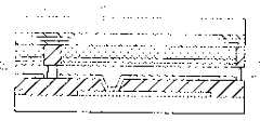
- H—ELECTRICITY
- H10—SEMICONDUCTOR DEVICES; ELECTRIC SOLID-STATE DEVICES NOT OTHERWISE PROVIDED FOR
- H10K—ORGANIC ELECTRIC SOLID-STATE DEVICES
- H10K71/00—Manufacture or treatment specially adapted for the organic devices covered by this subclass
Landscapes
- Engineering & Computer Science (AREA)
- Microelectronics & Electronic Packaging (AREA)
- Manufacturing & Machinery (AREA)
- Electroluminescent Light Sources (AREA)
- Devices For Indicating Variable Information By Combining Individual Elements (AREA)
Abstract
Translated fromChineseDescription
Translated fromChinese技术领域technical field
本发明涉及利用液晶显示装置等非发光显示装置、有机电致发光元件等发光显示装置等的显示装置、及其制造方法和驱动方法。尤其涉及在显示区内同时设有非发光显示区及发光显示区的显示装置,发光显示装置及其制造方法以及它的驱动电路。The present invention relates to a display device using a non-light-emitting display device such as a liquid crystal display device, a light-emitting display device such as an organic electroluminescent element, and a manufacturing method and a driving method thereof. In particular, it relates to a display device with a non-luminous display area and a light-emitting display area in the display area, a light-emitting display device, a manufacturing method thereof, and a driving circuit thereof.
背景技术Background technique
近年来,移动电话及移动信息终端(PDA:Personal Date Assistant,个人数据助理)等广泛普及。随之,近年,附带在这些终端上的用来显示信息的显示装置的研发在在广泛进行。In recent years, mobile phones and mobile information terminals (PDA: Personal Date Assistant, personal data assistant), etc. have been widely used. Accordingly, in recent years, research and development of display devices for displaying information attached to these terminals has been widely carried out.
上述的显示装置大致可分为非发光型显示装置与发光型显示装置二类,前者是将阳光、室内光、背景灯、正面光等的来自外部光源的光经光调制元件调整后进行显示,作为其代表,人们已知的是液晶显示元件;而后者则不必要有外部光源,靠发光元件自身发光来显示,作为其代表,电致发光器件(ElectroLuminescence)正受到人们十分关注,下面,对这些显示装置作进一步详细说明。The above-mentioned display devices can be roughly divided into two types: non-luminous display devices and luminous display devices. The former displays light from external light sources such as sunlight, indoor light, background light, and front light after being adjusted by light modulation elements. As its representative, liquid crystal display elements are known; and the latter does not need an external light source, and is displayed by the light-emitting element itself. As its representative, electroluminescent devices (ElectroLuminescence) are receiving great attention. Below, the These display devices are described in further detail.
首先,就利用外部光源的非发光型显示装置即透光式液晶显示装置来说,由于以背景灯作为光源,故消耗电力大、外形大,对于携带使用不利,因此,为了抑制上述问题之一的电力消耗,开发出一种将液晶层下部的电极用铝等的能反射光的金属来制作,以此,开发了作为光源利用太阳光及室内灯光等外部光源的反射型液晶显示装置。而这种反射型液晶显示装置是利用外部光源工作,所以难以在暗处使用。First of all, as for the non-luminous display device using external light sources, that is, the transmissive liquid crystal display device, since the backlight is used as the light source, the power consumption is large and the appearance is large, which is not good for carrying. Therefore, in order to suppress one of the above problems In order to reduce the power consumption, a reflective liquid crystal display device that uses external light sources such as sunlight and indoor lights as a light source has been developed by making the electrodes at the bottom of the liquid crystal layer out of light-reflecting metals such as aluminum. However, such a reflective liquid crystal display device operates by using an external light source, so it is difficult to use it in a dark place.
为了解决这一问题,开发了一种透光型显示装置,将液晶层下部电极用半透镜制成,在亮的环境下可不使用背景灯而进行反射型显示,而在暗的场所时,点亮背景灯进行透光型显示。但所述半透光型显示装置中,光反射的部分与光透过的部分使用了相反的特性,这就降低了光利用效率,因此,不能根本改善降低电力消耗。In order to solve this problem, a light-transmitting display device has been developed. The lower electrode of the liquid crystal layer is made of a semi-mirror. In a bright environment, a reflective display can be performed without using a backlight. Light the backlight for light-transmitting display. However, in the semi-transmissive display device, the light reflection part and the light transmission part use opposite characteristics, which reduces the light utilization efficiency, and therefore cannot fundamentally improve and reduce power consumption.
因此,本发明者研究了一种既能在亮环境下不用背景灯而作为反射型使用、在暗处时点亮背景灯而作为透光型使用的液晶娴熟装置(参照美国专利公报“Patent No.:US6,195,140B1,Date of Patent:Feb,27,2001”即日本国公开特许公报“特开平11-101992号公报(公开日,1999年4月13日)。Therefore, the present inventor has studied a kind of liquid crystal display device that can be used as a reflective type without a backlight in a bright environment, and as a transmissive type with a lighted backlight in a dark place (refer to U.S. Patent Publication "Patent No. .: US6,195,140B1, Date of Patent: Feb, 27, 2001" that is, the Japanese Open Patent Gazette "JP 11-101992 Gazette (public date, April 13, 1999).
该液晶显示装置与使用减少膜厚并使其具有半透光性的反射片的以往的液晶显示装置不同,在液晶显示装置中将各显示像素分反射区和透过区二个区,即所述液晶显示装置作为各显示像素的一个区,形成反射电极,并作为反射区;另一方面,在各显示像素的其他区中形成透过电极,一并设置定为透过区,另外使反射区的液晶层厚度与透过区的液晶层厚度不同,这样就可能在反射区和透过区的各个区内实现最佳亮度。This liquid crystal display device is different from the conventional liquid crystal display device that uses a reflective sheet that reduces the film thickness and makes it semi-transparent. The above-mentioned liquid crystal display device is used as a region of each display pixel to form a reflective electrode, which is used as a reflective region; The thickness of the liquid crystal layer in the reflective area is different from that in the transmissive area, so that it is possible to achieve optimum brightness in each of the reflective and transmissive areas.
然而在上述的像素分割型的液晶装置中,虽将背景灯从后方对各像素的整个区进行照射,而能够利用该背景灯的仅是各像素的透过区,因此存在着背景灯利用率低的问题,尤其是在反射电极的区比率高的情况下,必然透过区会变窄,故背景灯利用率降低。However, in the above-mentioned pixel division type liquid crystal device, although the backlight is used to irradiate the entire area of each pixel from the rear, and only the transmission area of each pixel can be utilized, so there is a low utilization rate of the backlight. Especially in the case of a high area ratio of the reflective electrode, the transmission area must be narrowed, so the utilization rate of the backlight is reduced.
作为提高上述像素分割型液晶显示装置的背景灯利用率的一例,例如有日本国公开将许报“特开2001-66593号公报(公开日2001年3月16日),公开的像素分割型液晶显示装置。在该液晶显示装置300中,如图41所示,首先,在液晶屏301的各像素302…上所配置的反射电极303一部分上设置透过开口部304…,由此形成像素分割型的液晶显示装置,另外,该液晶显示装置300中,作为背景灯采用由有机EL(电致发光)元件310组成的发光元件,另一方面该有机EL元件310的发光部311…不是配置在各像素302…的整个区上,只配置在对应于透过开口部304的区,这样,由于将作成图案的有机EL元件作为背景灯组入,提高了光的利用率,降低电力消耗。As an example of improving the utilization rate of the backlight of the above-mentioned pixel division type liquid crystal display device, for example, there is a Japanese publication "JP-A-2001-66593 (publication date: March 16, 2001), which discloses a pixel division type liquid crystal display device. Display device. In this liquid
在此,对于作为发光显示装置代表的、使用上述有机EL元件的显示装置,它具有薄、轻的特点,不用照光也能在暗处使用,并且,所发射的光几乎全部用于显示,所以光利用效率高,但是,这种用有机EL元件的显示装置必须经常发光,尤其在亮环境下为提高显示质量,必须增加其发光量,因此难以实现降低电耗。Here, as a representative light-emitting display device, a display device using the above-mentioned organic EL element is thin and light, can be used in a dark place without lighting, and almost all of the emitted light is used for display, so Light utilization efficiency is high, but such a display device using an organic EL element must always emit light. Especially in a bright environment, in order to improve the display quality, the amount of light emission must be increased, so it is difficult to reduce power consumption.
然而,在图41所示的像素分割型液晶显示装置中,为了在液晶屏301的外侧配置作为发光元件的有机EL元件310,在反射电极303的透过开口部304…与有机EL元件310之间,装有相差片305、偏振片306及二片玻璃基板即玻璃基板307及玻璃基板312。当今,一般像素间距为80μm左右,这种场合下,透过开口部104的宽度是它的1/2到1/6,约15μm至40μm,因此,偏振片306的厚度约为300μm,厚为500~700μm的玻璃以基板液晶屏301的玻璃基板307和有机EL元件310的玻璃基板312的形式存在。因此,反射电极303的透过开口部304与有机EL元件310之间的距离为1300μm~1700μm,因而尽管将有机EL元件310的发光体311设置在透过开口部304相对应的位置上,也不可能使有机EL元件310的发光体311所发出的光会全部射入透过开口部304,因此,依然存在着有机EL元件110照射效率不高的问题。However, in the pixel division type liquid crystal display device shown in FIG. Between them, a
又,图41所示的像素分割型液晶显示装置中,重叠基板这一点仍不变。此外,对于其薄形化方面,液晶显示装置厚度与有机EL元件厚度的总厚度有界限,故薄形化的问题仍然没有解决,还有,在图41结构的情况下,有必要将液晶显示装置的透过开口部304与有机EL元件310的形成部预先定位并固定,为此,必须要有专用的定位装置及固定用的机构,使得部件数目增加,成本上升。Also, in the pixel division type liquid crystal display device shown in FIG. 41, the point of overlapping substrates remains unchanged. In addition, in terms of its thinning, the thickness of the liquid crystal display device and the total thickness of the organic EL element have a limit, so the problem of thinning has not yet been solved. Also, in the case of the structure of FIG. 41, it is necessary to make the liquid crystal display The transmission opening 304 of the device and the forming part of the
另一方面,如上所述,反射型液晶显示装置是以提高室外的视觉识别性为目的而开发的,室外的光线强,视觉识别性当然优越,反之,它就不能在室内或晚间使用,因此,如果使用反射型液晶显示装置的话,作为外光的代用,相应要研究引入从前方照射的正面光,该对于正面光使用有机EL元件的示例公开在日本国公开特许公报“特开2000-75287号公报(公开日2000年3月14日)上,然而,这种场合也如在透过型液晶显示装置上导入背景灯的情况一样,存在着由于显示装置与辅助光源的厚度而致使整体厚度变厚的问题。On the other hand, as mentioned above, reflective liquid crystal display devices are developed for the purpose of improving outdoor visibility. The outdoor light is strong, and the visibility is of course superior. On the contrary, it cannot be used indoors or at night. Therefore, , if a reflective liquid crystal display device is used, as a substitute for external light, it is necessary to study the introduction of front light irradiated from the front. The example of using an organic EL element for the front light is disclosed in Japanese Patent Laid-Open Publication No. 2000-75287 However, in this case, as in the case of introducing a backlight on a transmissive liquid crystal display device, there is a problem that the overall thickness of the display device and the auxiliary light source is reduced. problem of thickening.
另外,如上所述,通过在一块底板上形成液晶显示元件及有机EL元件,从而能弥补各自的缺点,在各种情况下作最佳的显示。In addition, as described above, by forming the liquid crystal display element and the organic EL element on one substrate, it is possible to make up for their respective disadvantages, and to provide optimum display in each case.
但是,在上述显示装置中,若在一块底板上单纯形成液晶显示元件和有机EL元件,则底板的布线驱动电路变得复杂,制造成品率,成本等构成为问题。However, in the above-mentioned display device, if the liquid crystal display element and the organic EL element are simply formed on a single substrate, the wiring driving circuit on the substrate becomes complicated, and problems such as manufacturing yield and cost arise.
另一方面,作为其他的问题,对于具有作为发光元件的有机EL元件的发光显示装置,在进行制造时存在以下问题,On the other hand, as another problem, there are the following problems when manufacturing a light-emitting display device having an organic EL element as a light-emitting element.
例如在日本国公开特许公报“特开2000-173770号公报(公开日,2000年6月23日)公开了如下技术,在一块基板上,形成有机EL元件的驱动回路即TFT薄膜半导体电路,再在其上形成作为阴极的金属电极及形成有机EL层的有机层的一部分,再在另外一块基板上形成阳极层以后,再在其上形成发光层,最后,将双片基板叠合,通过加热或加压,使有机层在玻璃层转移温度以上的温度下接合。For example, the following technology is disclosed in Japan's patent publication "JP-A-2000-173770 (publication date, June 23, 2000). Form the metal electrode as the cathode and a part of the organic layer forming the organic EL layer on it, and then form the anode layer on another substrate, and then form the light-emitting layer on it. Finally, the two substrates are stacked and heated. Alternatively, pressure is applied to join the organic layers at a temperature equal to or higher than the glass transition temperature.
又,在日本国公开特许公报“特开2001-43980号公报(公开日,2001年2月16日)”中公开了下述技术,在基板上(TFT基板也可)先形成阳电极(阳极)在其上顺次叠层作为有机EL层的正孔注入层、正孔输送层及发光层,此后极薄地形成作为阴极的低工作函数的金属层,最后形成透明导电层。In addition, the following technology is disclosed in the Japanese Laid-Open Patent Publication "JP-A-2001-43980 (publication date, February 16, 2001)". An anode electrode (anode ) sequentially laminate the positive hole injection layer, the positive hole transport layer and the luminescent layer as the organic EL layer, and then form a metal layer with a low work function as the cathode very thinly, and finally form a transparent conductive layer.
这里,上述两公报任之一中,都使得从有机EL元件出射的光不是从形成该有机EL元件的驱动电回路的基板侧出射,而是从与其对向设定的对向基板或保护层一侧出射,这样,与从电路形成侧出射的场合相比,出射光不致被电路布线图案遮挡,因此可以加大开口率,提高壳度和发光效率,提高可靠性,延长使用寿命。Here, in any of the above-mentioned two publications, the light emitted from the organic EL element is not emitted from the substrate side forming the driving circuit of the organic EL element, but from the opposite substrate or protective layer set opposite to it. In this way, compared with the case of emitting from the side where the circuit is formed, the emitted light will not be blocked by the circuit wiring pattern, so the aperture ratio can be increased, the shell size and luminous efficiency can be improved, the reliability can be improved, and the service life can be extended.
另外,驱动电路的形成侧,甚至以往用作开口部的面积,这里也够形成电路,并留有电路设计的余地,在提高可靠性和成品率的同时,能够形成进一步增强功能的电路,具体地在上述特开2000-173770号公报中,通过分开形成驱动电路侧与发光层侧分开来实现,上述特开2001-43980号公报中,将阴极电极做得极薄来实现。In addition, on the formation side of the driving circuit, even the area used as the opening in the past is enough to form the circuit here, and there is room for circuit design. While improving reliability and yield, it is possible to form a circuit with further enhanced functions. In the aforementioned JP-A No. 2000-173770, this is achieved by forming the drive circuit side and the light-emitting layer side separately, and in the aforementioned JP-A No. 2001-43980, it is achieved by making the cathode electrode extremely thin.
这里,对于有机EL元件从发光功能的可靠性观点出发,要特别注意不要混入水分,再者,也有由于氧化,受主掺杂而导致有机导电体性能劣化,还有,作为阴极使用的金属有镁(mg)、锂(Li)、钙(Ca)等工作函数低的材料,特别容易氧化,成形加工困难。Here, for the organic EL element, from the viewpoint of the reliability of the light-emitting function, special care should be taken not to mix water. Furthermore, there are also cases where the performance of the organic conductor is deteriorated due to oxidation and acceptor doping. Also, the metal used as the cathode has Materials with low work functions such as magnesium (mg), lithium (Li), and calcium (Ca) are particularly prone to oxidation and difficult to form and process.
这样,有机EL元件虽然构造单纯,但特点在于,所用的材料性能容易受外周围环境的影响,因此在形成EL元件式,要尽量在隔断水分及氧气的环境下形成,并且最好同时形成保护发光层的保护层。In this way, although the structure of the organic EL element is simple, the characteristic is that the properties of the materials used are easily affected by the external environment. Protective layer for the luminescent layer.
这一点,在上述特开2000-173770号公报中,为了通过形成有机EL元件的有机层的一部分进行接合,因此在接合时暴露在含有水分和氧气的气氛中的可能性很大,故可靠性成为一个问题。In this regard, in the above-mentioned Japanese Unexamined Patent Application Publication No. 2000-173770, in order to form a part of the organic layer of the organic EL element for bonding, there is a high possibility of being exposed to an atmosphere containing moisture and oxygen during bonding, so reliability become a problem.
又,形成有机EL元件的有机层都用约1000左右的薄膜,贴合时在两基板侧上形成其一部分,在温度上升到玻璃转化点以上的过程中,膜质及其性能的均一性往往会受到破坏。In addition, the organic layer forming the organic EL element is made of a thin film of about 1000 Å, and a part of it is formed on the sides of the two substrates when bonding, and the uniformity of the film quality and its performance is guaranteed when the temperature rises above the glass transition point. tend to be damaged.
又,在上述特开2001-43980号公报中,在出射光的一侧有金属制的阴极,尽管极薄,也会存在由此引起的透过损耗,另外正因为阴电极极薄,因此,与形成在其上的透明导电层及有机导电层中含有的氧气结合而导致性能劣化、以及在形成透明导电层时的温度对发光层的影响,成为要研究的问题。Also, in the above-mentioned Japanese Patent Laid-Open No. 2001-43980, there is a metal cathode on the light-emitting side. Although it is extremely thin, there will be a transmission loss caused by it. In addition, because the cathode electrode is extremely thin, therefore, Combining with oxygen contained in the transparent conductive layer and the organic conductive layer formed thereon to cause performance degradation, and the influence of the temperature when forming the transparent conductive layer on the light-emitting layer have become issues to be studied.
又,根据上述特开2000-173770号公报,由于阳极侧为透明导电膜,比通常导体具有较高的阻抗,因此在做成屏板时,由于透明导电膜造成的电力损耗会引起图像画面产生光斑等问题。In addition, according to the above-mentioned Japanese Patent Application Laid-Open No. 2000-173770, since the anode side is a transparent conductive film, which has higher impedance than ordinary conductors, when it is made into a screen panel, the power loss caused by the transparent conductive film will cause the generation of an image. Spots and other issues.
发明内容Contents of the invention
本发明的目的在于,提供一种小型、低价且从在室外到室内视觉识别性均优良的显示装置及其制造和驱动方法。An object of the present invention is to provide a small, low-cost display device with excellent visibility from outdoors to indoors, and a method of manufacturing and driving the same.
为了达到以上目的,本发明的显示装置中,在显示区里,包括由光调制元件反射外来光来进行显示的非发光显示元件组成的第一显示区以及由发光元件直接调制并进行显示的显示元件组成的第二显示区,并同时设置上述第一显示区和第二显示区。In order to achieve the above object, in the display device of the present invention, in the display area, it includes a first display area composed of a non-luminous display element that reflects external light to display by a light modulation element, and a display area that is directly modulated and displayed by a light-emitting element. The second display area composed of components, and the above-mentioned first display area and the second display area are set at the same time.
因此,本发明的发光元件不同于以往那样地将发光元件作为背景灯和正面光来使用,而是向着显示面一侧以自身的发光直接进行显示。藉此可以提高发光元件所发出的光的利用率,同时也可使显示装置的厚度变薄,即是说,背背景灯景灯的厚度通常为3~6mm左右,因此,由于不采用背景灯而带来的厚度减小的优点是非常大的,首先,不需要背景灯是指,不需要以往的设置在液晶屏的背面与背景灯之间偏振片、相差片以及玻璃基板。因此,由于不需要这些偏振片、相差片和玻璃基板变得均不,显示装置的厚度可以更加薄。Therefore, the light-emitting element of the present invention is different from the conventional use of the light-emitting element as a backlight and a front light, and displays directly by its own light emission toward the display surface side. In this way, the utilization rate of the light emitted by the light-emitting element can be improved, and at the same time, the thickness of the display device can be thinned. The advantage of reducing the thickness is very large. First, no backlight is required, which means that there is no need for polarizers, phase difference plates, and glass substrates that were installed between the back of the LCD screen and the backlight. Therefore, since these polarizing plates, phase difference plates, and glass substrates do not need to be uniform, the thickness of the display device can be thinner.
又,由于不必对形成图案的发光元件的背景灯进行定位,可以省略为此而备的专用装置、固定机构,则可减少部件数量、缩减工序,由此,可以降低成本支出。Moreover, since it is not necessary to position the backlight of the patterned light-emitting element, special devices and fixing mechanisms prepared for this purpose can be omitted, and the number of parts and processes can be reduced, thereby reducing costs.
而且,不需要背景灯与背面侧偏振片及相差片的优点在于,不仅限于显示装置整体厚度的变薄,也就是说,减少部件数量这一点来讲不仅对于材料费,而且组装人工数和各种部件检查等所需费用也能削减,故显示装置整体上的制造成本下降。Furthermore, the advantage of not requiring a backlight, a polarizing plate on the rear side, and a phase difference plate is not only limited to the thinning of the overall thickness of the display device, that is, the reduction in the number of parts is not only for the cost of materials, but also for the number of assembly labor and each The cost required for inspection of various parts can also be reduced, so that the manufacturing cost of the display device as a whole can be reduced.
还有,对于发明那样的例如像素分割方式等的显示区分割方式的显示装置,能够将第一显示区与第二显示区之比任意地设定为一定程度,由此,例如在使用于手机、信息携带终端(PDA)等移动设备中的场合下,通常,将反射区即第一显示区的比率增大,例如使得显示像素的像素面积中80%为反射区时,发光区即第二显示区为20%,因此发光元件的发光面积即使为最大也只需像素面积的1/5就可以了,这一点意味着能够减少电力消耗。In addition, for the display device of the display area division method such as the pixel division method as in the invention, the ratio of the first display area to the second display area can be set to a certain degree arbitrarily, thereby, for example, when used in a mobile phone , information portable terminal (PDA) and other mobile devices, generally, the ratio of the reflective area, that is, the first display area, is increased, for example, when 80% of the pixel area of the display pixel is the reflective area, the light-emitting area, that is, the second The display area is 20%, so even if the light-emitting element's light-emitting area is the largest, it only needs 1/5 of the pixel area, which means that power consumption can be reduced.
因此,能提供一种小型、廉价,同时无论野外或室内其视觉识别性能均优越的显示装置。Therefore, it is possible to provide a display device that is small, inexpensive, and excellent in visual recognition performance outdoors or indoors.
又,本发明的显示装置还具有相互对向的第一基板和第二基板,所述光调整元件及发光元件都设置在所述第一基板和第二基板之间,因而将光调制元件及发光元件都仅收容在第一基板和第二基板之间,从而使显示装置的厚度能确实减薄。In addition, the display device of the present invention further has a first substrate and a second substrate facing each other, and the light adjustment element and the light emitting element are arranged between the first substrate and the second substrate, so that the light modulation element and the light emitting element The light-emitting elements are only accommodated between the first substrate and the second substrate, so that the thickness of the display device can be reliably reduced.
又,本发明的显示装置是在所述记载的显示装置内,光调整元件的光调制层与发光元件的发光层同层设置,这里所谓的同层并不意味为同一水平位置,在发光元件的光调制层内可包含发光元件的发光层。Moreover, in the display device of the present invention, in the display device described above, the light modulation layer of the light adjustment element and the light-emitting layer of the light-emitting element are arranged on the same layer, and the so-called same layer here does not mean the same horizontal position, and the light-emitting element A light-emitting layer of a light-emitting element may be included in the light-modulating layer.
根据所述发明,发光元件与光调制元件的光调制层设置在同一层,因此,在以往由光调制元件形成的非发光显示元件的厚度范围内,能够收容发光元件,结果能确实地减薄显示装置的厚度。According to the above-mentioned invention, since the light-modulating layer of the light-emitting element and the light-modulating element is provided on the same layer, the light-emitting element can be accommodated within the thickness range of the conventional non-light-emitting display element formed by the light-modulating element, and as a result, the thickness can be reliably reduced. Displays the thickness of the device.
又,本发明的显示装置,在其显示区内一并设置由光调制元件反射外光进行显示的非发光显示元件所组成的第一显示区、发光元件直接调制并进行显示的发光显示元件所组成的第二显示区,同时还具备相相互对设置的第一基板和第二基板,所述光调制元件及发光元件都设置在第一基板与第二基板之间,并且在所述第二显示区内,在所述第一基板上顺次叠层所述发光元件和光调制元件的光调制层。Also, in the display device of the present invention, a first display area composed of non-luminous display elements that reflect external light for display by light modulation elements and a light-emitting display element that directly modulates and displays light-emitting elements are provided in the display area. The second display area is composed of a first substrate and a second substrate opposite to each other, the light modulation element and the light emitting element are both arranged between the first substrate and the second substrate, and the second substrate In the display area, the light modulation layer of the light emitting element and the light modulation element is sequentially laminated on the first substrate.
根据所述发明,在第二显示区内,在所述第一基板上所述发光元件和光调制元件的光调制层顺次叠层,因此,光调制元件及发光元件都被收容在第一基板与第二基板之间,因此显示装置的厚度能确实减薄,并且,尽管光调制层可在发光元件的表面侧层叠,发光元件被设置在第一基板与第二基板之间,因此,发光元件的显示光全部出射到第二显示区。因而,光的利用率非常高。According to the above-mentioned invention, in the second display area, the light modulation layers of the light-emitting element and the light-modulating element are sequentially laminated on the first substrate, so that the light-modulating element and the light-emitting element are both accommodated on the first substrate. and the second substrate, so the thickness of the display device can be surely reduced, and, although the light modulation layer may be laminated on the surface side of the light emitting element, the light emitting element is provided between the first substrate and the second substrate, and therefore, emits light All the display light of the element is emitted to the second display area. Therefore, the utilization efficiency of light is very high.
由此,能够提供一种确保更高照射效率、不仅提高亮度且能减少显示装置厚度以及降低部件费用的显示装置。Accordingly, it is possible to provide a display device that ensures higher irradiation efficiency, improves luminance, reduces thickness of the display device, and reduces component costs.
又,本发明的显示装置能够相互共用以所述光调制元件及发光元件驱动矩阵状配置的所述各显示区的各数据信号线及各扫描信号线。In addition, the display device of the present invention can share the data signal lines and the scanning signal lines of the respective display regions arranged in a driving matrix with the light modulation elements and light emitting elements.
因此,能够提供一种在显示区内形成两个显示元件时可防止电路构成复杂化、并且制造成品率高且成本低的显示装置。Therefore, it is possible to provide a low-cost display device that prevents the circuit configuration from being complicated when two display elements are formed in the display region, and that has high manufacturing yield.
又,本发明的显示装置的制造方法,在制造所述的非发光显示元件与发光显示元件并用的显示装置时,当在第一基板上形成驱动电路,在第二基板上形成发光元件后,将形成这些驱动电路的第一基板侧和形成发光元件的第二基板侧相合成一体。In addition, in the method for manufacturing a display device of the present invention, when manufacturing the display device in which the above-mentioned non-luminescent display element and light-emitting display element are used together, after forming a driving circuit on the first substrate and forming a light-emitting element on the second substrate, The first substrate side on which these drive circuits are formed and the second substrate side on which the light emitting elements are formed are integrated.
在制造显示装置时,可将发光元件及驱动发光元件和光调制元件的驱动元件以另外方法形成,因此,在发光元件形成时不会受到驱动元件形成时的工序温度、药品、气体等的影响。When manufacturing a display device, the light-emitting element and the driving element for driving the light-emitting element and the light modulation element can be formed separately, so the formation of the light-emitting element will not be affected by the process temperature, chemicals, gases, etc. during the formation of the driving element.
又,本发明的显示装置,为了解决上述问题,由显示元件单独形成,在第一基板上形成了驱动电路的第一基板侧、与在第二基板上形成包括二个发光元件用电极在内的发光元件成的第二基板侧贴合在一起。Also, the display device of the present invention, in order to solve the above-mentioned problems, is formed by the display element alone, the first substrate side of the driving circuit is formed on the first substrate, and the electrode including two light-emitting elements is formed on the second substrate. The light-emitting elements are bonded together into the second substrate side.
又,本发明的显示装置,在所述记载的显示装置中,发光元件由有机电致发光元件形成,在形成所述有机电致发光元件的第二基板侧,在有机电致发光元件上的阴极形成之后,与第一基板侧贴合在一起。In addition, in the display device of the present invention, in the display device described above, the light-emitting element is formed by an organic electroluminescent element, and on the side of the second substrate where the organic electroluminescent element is formed, on the organic electroluminescent element After the cathode is formed, it is bonded together with the first substrate side.
根据所述发明,对于单由发光元件形成的装置,形成作为发光元件的有机电致发光元件(以下称作“有机EL元件”)的第二基板侧,在有机EL元件上作为发光元件用电极的阴极电极形成以后,与第一基板侧贴合在一起。According to the above-mentioned invention, for a device formed of only a light-emitting element, the second substrate side of an organic electroluminescence element (hereinafter referred to as "organic EL element") as a light-emitting element is formed, and an electrode for a light-emitting element is formed on the organic EL element. After the cathode electrode is formed, it is bonded together with the first substrate side.
藉此,使从有机EL元件出射的光不是从驱动有机EL元件的驱动电路的基板侧出射,而从与其对向设置的对向基板或保护层侧出射,因此,与所述以往技术中的光出射方向相同,与向驱动电路形成侧出射的构造相比,同样地具有下述基本优点。Thereby, the light emitted from the organic EL element is not emitted from the substrate side of the driving circuit for driving the organic EL element, but emitted from the opposite substrate or the protective layer side provided opposite to it. Therefore, it is different from the prior art. The direction of light emission is the same, and compared with the structure in which the light is emitted toward the side where the driving circuit is formed, it also has the following basic advantages.
首先,由于分别形成设置驱动电路的第一基板侧与有机EL元件。因此,可以分别独立地组合制造工序,因而不受温度、气体以及药品等的影响,提高了可靠性。First, since the first substrate side where the drive circuit is provided and the organic EL element are formed separately. Therefore, the manufacturing processes can be combined independently, so that they are not affected by temperature, gas, chemicals, etc., and the reliability is improved.
又,由于所述结构,可以使光出射到形成了有机EL元件的第二基板侧,这样,可以不影响驱动电路侧的开口率而将发光区设定为更宽。由此,能提高亮度,而且由于发光面积较大,获得相同亮度所需的每单位面积电流量可降低,则可以实现延长使用寿命、以及利用发光效率提高来减少电能消耗。Also, due to the above structure, light can be emitted to the second substrate side where the organic EL element is formed, so that the light emitting area can be set wider without affecting the aperture ratio on the drive circuit side. Therefore, the brightness can be improved, and since the light-emitting area is larger, the amount of current per unit area required to obtain the same brightness can be reduced, so that the service life can be extended and the power consumption can be reduced by improving the luminous efficiency.
又,由于光出射到形成有驱动电路的第一基板侧,第一基板侧可以在整个面上形成驱动电路,因此,能够自由设定驱动电路的TFT(Thin FilmTransistor,薄膜晶体管)的大小,或在TFT生成区上留有余地,从而能形成需要紧密控制的电路,另外,由于布线宽度也有了余地,使驱动电路可靠性更高,成品合格率也更高。Also, since the light is emitted to the first substrate side on which the driving circuit is formed, the driving circuit can be formed on the entire surface of the first substrate side, so the size of the TFT (Thin Film Transistor, thin film transistor) of the driving circuit can be freely set, or There is room in the TFT generation area, so that circuits that need to be tightly controlled can be formed. In addition, because there is room for wiring width, the reliability of the driving circuit is higher, and the yield of finished products is also higher.
又,在本发明的显示装置的驱动方法中,采用一并设置非发光显示元件与发光显示元件的显示装置,并且,将各显示区内的图像信号的单位时间即1个场分割成多个,在每个各分割其间使光调制元件或发光元件进行通—断动作。Also, in the method for driving a display device according to the present invention, a display device in which a non-light-emitting display element and a light-emitting display element are provided together is used, and one field, which is a unit time of an image signal in each display area, is divided into a plurality of , make the light modulation element or light emitting element perform on-off operation during each division.
根据所述发明,对于一并设置驱动非发光显示元件与发光显示元件的显示装置,通过将1个场分割成几个,在每个分割期间令光调制元件或发光元件进行通—断动作,可以控制1个场中的光调制元件或发光元件的总导通时间,进一步使这种点灯布线图案的种类多样化,并且能有效地进行驱动。According to the above invention, in a display device in which a non-luminous display element and a light-emitting display element are driven together, by dividing one field into several, the light modulation element or the light-emitting element is turned on-off in each divided period, The total ON time of the light modulation elements or light emitting elements in one field can be controlled, and the types of such lighting wiring patterns can be further diversified and driven efficiently.
又,通过上述时间上控制光调制元件或发光元件的导通时间,能够显示图像信号的灰度等级。In addition, by temporally controlling the conduction time of the light modulation element or the light emitting element as described above, it is possible to display the gradation of the image signal.
因此,当两个显示元件形成在一个显示区内时,要防止电路构造复杂化,能提供一种制造时合格率高、低成本、效率高,并能有良好灰度等级显示的显示装置的驱动方法。Therefore, when two display elements are formed in one display area, it is necessary to prevent the circuit structure from being complicated, and to provide a display device with high yield, low cost, high efficiency, and good gray scale display during manufacture. drive method.
本发明的其他目的,特微和优点详见以不记载就可充分了解,另外,关于本发明的优点参照附图并阅读以下说明,可以明确。Other objects, features and advantages of the present invention can be fully understood by referring to the details without description. In addition, the advantages of the present invention can be clarified by reading the following description with reference to the accompanying drawings.
附图说明Description of drawings
图1是表示本发明的显示装置一实施形态,它是表示该表示显示装置中一个像素的断面图。Fig. 1 shows an embodiment of a display device according to the present invention, and is a cross-sectional view showing a pixel in the display device.
图2是表示本发明概要,它是表示显示环境与消耗电能的关系图。Fig. 2 shows the outline of the present invention, and it is a diagram showing the relationship between the display environment and the power consumption.
图3是表示本发明概要,它是表示显示环境与亮度的关系图。Fig. 3 shows the outline of the present invention, and is a diagram showing the relationship between the display environment and brightness.
图4(a)~图4(c)是表示所述显示装置中的对向基板的制造方法的说明图。4( a ) to 4( c ) are explanatory diagrams showing a method of manufacturing the counter substrate in the display device.
图5(a)及图5(b)是表示所述显示装置中TFT基板制造方法的说明图。5( a ) and FIG. 5( b ) are explanatory diagrams showing a method of manufacturing a TFT substrate in the display device.
图6是表示将金属电极沿有机EL元件的阳极在黑色矩阵下形成显示装置断面图。Fig. 6 is a cross-sectional view showing a display device formed by forming a metal electrode along an anode of an organic EL element under a black matrix.
图7是表示将金属电极形成在有机EL元件的层构造上并在黑色矩阵下形成的显示装置断面图。7 is a cross-sectional view showing a display device in which metal electrodes are formed on the layer structure of an organic EL element and formed under a black matrix.
图8(a)及图8(b)是表示所述显示装置的对向基板与TFT基板贴合状态的说明图。8( a ) and FIG. 8( b ) are explanatory diagrams showing the bonding state of the counter substrate and the TFT substrate of the display device.
图9是所述显示装置中共用信号线并进行驱动时的1个像素的驱动电路图。FIG. 9 is a drive circuit diagram of one pixel when the signal line is shared and driven in the display device.
图10是表示所述显示装置在共用信号线并进行驱动时一个像素的驱动电路的变形例的驱动电路图。FIG. 10 is a drive circuit diagram showing a modified example of a drive circuit for one pixel when the display device is driven using a common signal line.
图11是表示所述显示装置的显示状态特性图。FIG. 11 is a graph showing display state characteristics of the display device.
图12表示本发明的显示装置的另一实施形态,它是表示显示装置中的一个像素的断面图。Fig. 12 shows another embodiment of the display device of the present invention, which is a cross-sectional view showing one pixel of the display device.
图13(a)~图13(c)是表示所述显示装置中对向基板制造方法的说明图。13( a ) to 13( c ) are explanatory diagrams showing a method of manufacturing a counter substrate in the display device.
图14是表示所述显示装置中TFT基板制造方法的说明图。FIG. 14 is an explanatory view showing a method of manufacturing a TFT substrate in the display device.
图15(a)及图15(b)是表示所述显示装置的对向基板与TFT基板贴合状态的说明图。15( a ) and FIG. 15( b ) are explanatory diagrams showing the bonded state of the counter substrate and the TFT substrate of the display device.
图16是表示本发明的显示装置再一实施形态表示显示装置中的一个像素的断面图。Fig. 16 is a cross-sectional view showing one pixel of the display device according to still another embodiment of the display device of the present invention.
图17是表示多层形成所述显示装置的凸部时的断面图。Fig. 17 is a cross-sectional view showing a case where the protrusions of the display device are formed in multiple layers.
图18是所述显示装置中显示画面的平面图。Fig. 18 is a plan view of a display screen in the display device.
图19(a)是表示将所述显示装置的1个像素的反射区及发光区进行分割时将发光区设置在反射区的内侧所构成的平面图。Fig. 19(a) is a plan view showing a configuration in which the reflection region and light emission region of one pixel of the display device are divided and the light emission region is provided inside the reflection region.
图19(b)是表示将所述显示装置的1个像素的反射区和发光区进行分割时,将发光区设置在反射区的边角侧所构成的平面图。Fig. 19(b) is a plan view showing a configuration in which the light-emitting region is provided at the corner side of the reflection region when the reflection region and light-emitting region of one pixel of the display device are divided.
图20是表示本发明的显示装置的再一实施形态,使用光传感器场合下的方框图。Fig. 20 is a block diagram showing still another embodiment of the display device of the present invention, in which an optical sensor is used.
图21是表示本发明的显示装置的再一实施形态,表示显示装置中一个像素的平面图。Fig. 21 shows still another embodiment of the display device of the present invention, showing a plan view of one pixel in the display device.
图22是所述显示装置中表示1个像素的图21的A-A线断面图。FIG. 22 is a sectional view along line A-A of FIG. 21 showing one pixel in the display device.
图23是表示所述显示装置的整体构成图。FIG. 23 is a diagram showing the overall configuration of the display device.
图24是表示所述显示装置在正常白色模式下漏电压Vd小于液晶用阈值电压Vth(LC)时液晶显示元件及有机EL元件的显示状态的说明图。24 is an explanatory view showing the display state of the liquid crystal display element and the organic EL element when the drain voltage Vd is lower than the threshold voltage Vth(LC) for liquid crystal in the normal white mode of the display device.
图25是表示所述显示装置在正常白色模式下漏电压Vd大于液晶用阈值电压Vth(LC)而小于EL元件的显示状态的说明图。25 is an explanatory diagram showing a display state in which the drain voltage Vd is higher than the threshold voltage Vth(LC) for liquid crystal and lower than the EL element in the normal white mode of the display device.
图26是表示所述显示装置在正常白色模式下,漏电压Vd大于液晶用阈值电压Vth(LC)并大于EC用阈值电压(OLED)时液晶显示元件及有机EL元件的显示状态的说明图。26 is an explanatory view showing the display state of the liquid crystal display element and the organic EL element when the drain voltage Vd is greater than the threshold voltage Vth (LC) for liquid crystal and greater than the threshold voltage for EC (OLED) in the normal white mode of the display device.
图27是表示所述显示装置在正常黑色模式下漏电压Vd小于共用阈值电压Vth时液晶显示元件及有机EL元件的显示状态的说明图。27 is an explanatory view showing the display state of the liquid crystal display element and the organic EL element when the drain voltage Vd is lower than the common threshold voltage Vth in the normal black mode of the display device.
图28是表示所述显示装置在正常黑色模式下漏电压Vd大于共用阈值电压Vth时液晶显示元件及有机EL元件的显示状态的说明图。28 is an explanatory view showing the display state of the liquid crystal display element and the organic EL element when the drain voltage Vd is higher than the common threshold voltage Vth in the normally black mode of the display device.
图29(a)是表示显示装置在正常黑色模式下液晶显示元件的亮度状态的说明图,图29(b)是表示显示装置在正常黑色模式下有机EL元件的亮度状态的说明图。29( a ) is an explanatory diagram showing the luminance state of the liquid crystal display element in the normally black mode of the display device, and FIG. 29( b ) is an explanatory diagram showing the luminance state of the organic EL element in the normally black mode of the display device.
图30是本发明的显示装置的另一其他实施形态下驱动时的信号波形图。Fig. 30 is a signal waveform diagram during driving in another embodiment of the display device of the present invention.
图31是表示电压电流转换手段的其他构成的说明图。Fig. 31 is an explanatory diagram showing another configuration of the voltage-current converting means.
图32(a)~图32(c)是本发明的显示装置的另一其他实施形态下驱动时的信号波形图。32(a) to 32(c) are signal waveform diagrams during driving in another embodiment of the display device of the present invention.
图33是表示本发明的显示装置另一其他实施形态,作为有机EL层由空穴输送层、发光层、电子输送层构成的有机EL发光元件的断面图。33 is a cross-sectional view of an organic EL light-emitting element composed of a hole transport layer, a light-emitting layer, and an electron transport layer as an organic EL layer in another embodiment of the display device of the present invention.
图34是表示由作为有机EL层的高分子EL材料构成的有机EL发光元件的断面图。Fig. 34 is a cross-sectional view showing an organic EL light-emitting element composed of a polymer EL material as an organic EL layer.
图35(a)~图35(c)是表示图33中所示的显示装置的对向基本反的制造方法的断面图。35( a ) to 35 ( c ) are cross-sectional views showing a substantially reversed manufacturing method of the display device shown in FIG. 33 .
图36(a)及图36(b)是表示图33中所示的显示装置的TFT电路侧基板的制造方法的断面图。36(a) and 36(b) are cross-sectional views showing a method of manufacturing the TFT circuit-side substrate of the display device shown in FIG. 33 .
图37(a)及图37(b)是表示图33中所示的显示装置的对向基板与TFT电路侧基板贴合工艺的断面图。37( a ) and 37 ( b ) are cross-sectional views showing the bonding process of the counter substrate and the TFT circuit side substrate of the display device shown in FIG. 33 .
图38(a)~图38(c)是表示图34所示的显示装置的对向基板的制造方法的断面图。38( a ) to 38 ( c ) are cross-sectional views showing a method of manufacturing the counter substrate of the display device shown in FIG. 34 .
图39是表示图34所示的显示装置TFT电路侧基板制造方法断面图。39 is a sectional view showing a method of manufacturing the TFT circuit-side substrate of the display device shown in FIG. 34 .
图40(a)及图40(b)是表示图34所示的显示装置的对向基板与TFT电路侧基板贴合工艺的断面图。40( a ) and 40 ( b ) are cross-sectional views showing the bonding process of the counter substrate and the TFT circuit side substrate of the display device shown in FIG. 34 .
图41是表示历来的显示装置的断面图。FIG. 41 is a cross-sectional view showing a conventional display device.
具体实施方式Detailed ways
首先,对于本发明的概要进行说明。First, the outline of the present invention will be described.
本发明的显示装置是将反射外光进行显示的非发光显示元件和自发光的发光显示元件在同一个显示装置内组装构成,由此可知,不需要装设背景灯等另外的光源,因此电力消耗低及小型化能同时实现,还有,将非发光显示元件和自发光的发光显示元件组合装设在同一个显示装置内,由于能够将电极、布线、驱动元件、绝缘体等的部件的制造工序共同化,因此,使以往用于背景灯等光源制造以及附件等所化费的时间和费用大幅降低。The display device of the present invention is assembled in the same display device with non-luminous display elements that reflect external light for display and self-luminous light-emitting display elements. It can be seen from this that there is no need to install additional light sources such as backlights, so the power consumption is reduced. Low consumption and miniaturization can be realized at the same time. In addition, the non-luminous display element and the self-luminous light-emitting display element are combined and installed in the same display device, because the manufacture of electrodes, wiring, driving elements, insulators, etc. The process is common, so the time and cost that were previously used in the manufacture of light sources such as backlights and accessories are greatly reduced.
以下,进一步对本发明的作用,效果等详细说明。Hereinafter, the action, effect, etc. of the present invention will be further described in detail.
首先,如上所述,通常显示装置大体上可分为非发光显示装置及发光显示装置二大类,非发光显示装置使从阳光、室内光、背景灯、正面光等外部光源出射的光透过非发光显示元件的光调制元件而进行调制,对于该非发光的显示元件,存在一种具有使得来自外部的光反射的反射手段的反射型、以及不具有反射手段的透过型。另一方面,发光显示装置是具有发光元件的显示装置,通常,发光元件或称为发光层的部分自动发光,这里,将上述光调制元件中透过光的控制称为光调制,与此相应,对发光元件的发光称为直接调制。First of all, as mentioned above, generally display devices can be roughly divided into two categories: non-luminous display devices and light-emitting display devices. Non-luminous display devices transmit light emitted from external light sources such as sunlight, indoor light, background light, and front light Modulation is performed by using a light modulation element of a non-luminescent display element. As for the non-luminous display element, there are a reflective type having reflective means for reflecting light from the outside, and a transmissive type without reflective means. On the other hand, a light-emitting display device is a display device having a light-emitting element. Usually, the light-emitting element or a part called a light-emitting layer emits light automatically. Here, the control of the transmitted light in the above-mentioned light modulating element is called light modulation, corresponding , The light emission of light-emitting elements is called direct modulation.
对于由透过型液晶显示装置所代表的透过型非发光显示装置,通常从暗显示到亮显示,背景灯的亮度是一定并经常点亮着,因此,透过型的非发光显示装置经常靠外部光源,会消耗电力,另外,透过型非发光显示装置的情况下,对光调制元件及背光灯而言必须要有多种电源供给及控制,因此部件多,限制了小型化,也非以降低成本。For the transmissive non-luminous display device represented by the transmissive liquid crystal display device, usually from dark display to bright display, the brightness of the backlight is constant and often lit, therefore, the transmissive non-luminous display device is often Relying on an external light source will consume power. In addition, in the case of a transmissive non-luminous display device, it is necessary to supply and control various power sources for the light modulation element and the backlight. Therefore, there are many components, which limits the miniaturization and not to reduce costs.
而另一方面,由EL显示装置代表的发光显示装置,为了调控发光亮度,暗显示和亮显示消耗的电力不同,从消耗电力来讲,暗显示少而亮显示则多。On the other hand, in light-emitting display devices represented by EL display devices, in order to control the luminance of light emission, the power consumption of dark display and bright display is different. In terms of power consumption, dark display is less and bright display is more.
这里,将这些透过型的非发光显示元件或发光显示元件和反射型的非发光显示元件组装在同一个屏内,将双方用于显示时,与本发明相比较。即将透过型的非发光显示元件与反射型的非发光显示元件组合的以往的显示装置,即作为以往技术已经说明过的像素分割型的液晶显示装置,以及本发明的显示装置一起作一比较。Here, when these transmissive non-luminous display elements or light-emitting display elements and reflective non-luminous display elements are assembled in the same panel, and both are used for display, a comparison is made with the present invention. A conventional display device that combines a transmissive non-luminous display element with a reflective non-luminous display element, that is, a pixel division type liquid crystal display device that has been described as the prior art, and the display device of the present invention will be compared together. .
以往的液晶显示装置如图2中用虚线L1所示,从亮环境下到暗环境下光源即背光灯必须常时点亮,必须消耗大体一定的电力,与此相比,将发光显示元件和反射型非发光显示元件组合在同一屏板中的本发明的显示装置可以根据周围环境来调整发光显示元件的亮度,因此,如图2实线L2所示那样,在亮环境下使发光亮度降低,使反射型的非发光显示元件得到最大限度的利用,而在暗环境下可使发光显示元件的发光亮度提高以保持显示,因此,亮环境下使以往透过型非发光显示装置中点亮背景灯的耗电减少。In the conventional liquid crystal display device, as shown by the dotted line L1 in FIG. 2, the light source, that is, the backlight, must always be turned on from the bright environment to the dark environment, and a substantially constant amount of power must be consumed. Compared with this, the light-emitting display element and the The display device of the present invention in which reflective non-luminous display elements are combined in the same panel can adjust the brightness of the light-emitting display elements according to the surrounding environment. Therefore, as shown by the solid line L2 in Figure 2, the luminous brightness is reduced in a bright environment. , so that the reflective non-luminous display elements can be utilized to the maximum extent, and the luminous brightness of the luminous display elements can be increased to maintain the display in a dark environment. The power consumption of the backlight is reduced.
因此,本发明的显示装置,如在亮环境下使用,比透过型的非发光显示元件与反射型的非发光显示元件组合的显示装置更为省电,通过降低亮度进行显示,能延长使用寿命,提高可靠性。还有,本发明的显示装置,没有必要另外设置背景灯,因此与以往的液晶显示装置比较,能实现薄型化和小型化,加上不需要供电手段和控制等,可以使成本降低。Therefore, if the display device of the present invention is used in a bright environment, it is more power-saving than a display device in which a transmissive non-luminous display element and a reflective non-luminous display element are combined, and the display can be extended by reducing the brightness. life and improve reliability. In addition, the display device of the present invention does not need to provide an additional backlight, so it can be thinned and miniaturized compared with conventional liquid crystal display devices. In addition, power supply means and controls are not required, and the cost can be reduced.
又,将本发明的显示装置与光用发光显示元件的显示装置比较,可得到图3的结果,即如图3中用虚线L1所显示的那样,光有发光显示元件构成的显示装置随着环境变得亮,其发光亮度如不增强,显示将变得难以辨认。Again, the display device of the present invention is compared with the display device of the light-emitting display element, and the result of FIG. 3 can be obtained, that is, as shown by the dotted line L1 in FIG. The environment becomes brighter, and the display becomes illegible unless its luminous brightness is enhanced.
而本发明的显示装置,在亮的环境下,反射型的非发光显示元件要提高其显示特性,发光显示元件如同一图的实线L2所示,亮度降低就能显示,这是以往仅用发光显示元件的场合下没有的内容,是本发明独自形成的亮度控制方法。However, in the display device of the present invention, in a bright environment, the reflective non-luminous display element should improve its display characteristics, and the light-emitting display element can be displayed with reduced brightness as shown by the solid line L2 in the same figure. What is not included in the case of a light-emitting display element is the luminance control method independently developed by the present invention.
这样,用于本发明的显示装置,比只用发光显示元件的情况,可将最大亮度设定得更低,同时能提高其使用的可靠性延长寿命。In this way, the display device used in the present invention can set the maximum luminance lower than the case of using only light-emitting display elements, and at the same time can improve the reliability of its use and prolong its life.
实施形态1
本发明的实施形态,按图4至图11说明如下。Embodiments of the present invention are described below with reference to FIGS. 4 to 11. FIG.
如图1所示,本实施形态的显示装置50,作为光调制层的液晶层26及作为发光元件的有机EL元件60,被上下方的TFT基板51及对向基板52挟在中间,而下方侧是在由玻璃为代表的材料形成的作为第一基板的绝缘性基板21上形成有TFT(Thin Film Trainmaster,薄膜晶体管),并且对于每个显示像素形成驱动作为光调制元件的反射型液晶显示元件20的液晶用TFT元件22及驱动作为发光元件的发光型有机EL元件60的EL用TFT元件4。这些液晶用TFT元件22及EL用TFT元件42能各自单独地进行驱动,另一方面,也可以共用信号线驱动。As shown in FIG. 1, in the
另一方面,在上方侧设有,同样由玻璃形成的透明的作为第二基板的绝缘性基板29;在该绝缘性基板29上又形成彩色滤色层28;黑色底层33;作为光调制元件显示面侧电极的对向电极27;由作为发光元件用电极及发光元件显示面侧电极的阴极65;空穴输送层64;发光层63;电子输送层62;以及由作为发光元件用电极的阴极61等组成的有机EL元件60、偏振片32、相差片31所组成的对向基板52。On the other hand, on the upper side, a transparent insulating
这里,本实施形态中,有机EL元件60与液晶显示元件20的光调制层即液晶层26设置在同一层并使在有机EL元件60的光出射侧不存在液晶层26。Here, in this embodiment, the
也就是说,本实施形态中的显示装置50中,对于作为显示区的每一个显示像素,一并设置有在液晶显示元件的一部分上将来自显示面一侧的外来入射光用液晶显示元件20的像素电极25反射并经液晶层26调制和显示的作为第一显示区的反射区11、以及在有机EL元件60的一部分上进行自发光并把该光向显示面一侧出射的作为第二显示区的发光区12a。That is to say, in the
又,本实施形态的显示装置50具有有机EL元件60出射的光难以穿透液晶层26的构造,因此,有机EL元件60出射的光,由于液晶的原因,没有被散射或被吸收,故难以产生亮度降低。Moreover, the
本实施形态中,所述有机EL元件60形成于对向基板52的阳极65上,这意味着实施形态的有机EL元件60通过与TFT电路不同工序加以制造。In the present embodiment, the
也就是说,有机EL元件60形成在对向基板52侧,形成后的EL元件60的光射向对向基板52侧,这样,在形成对向基板52之际,例如用ITO(indiumTin Oxide:,铟锡氧化物)形成透明的阳极65,然后依次序形成空穴输送层64、发光层63、电子输送层62、以及阴极61,可以采用以往所用的形成方法,同时由于对向基板52侧没有驱动电路,所以也就没有驱动电路而对有机EL元件60开口率进行限制,所以可以得到近100%的开口率。That is to say, the
又,由于TFT制造工序与对向基板52的制造工序分离,以避免TFT制造过程中产生的热影响,特别要有进行光刻及蚀刻的工序分开,它的药液和水会产生使用有机材料的发光层63特性劣化的有害作用。Moreover, since the TFT manufacturing process is separated from the manufacturing process of the
因此,将有机EL元件60与TFT基板51分开制成对于维持有机EL元件60的性能是有益的。Therefore, forming the
这里,本实施形态中使用的发光层,且不问是采用低分子型EL材料还是采用高分子型EL材料,该图表示的有机EL元件60是表示用低分子型EL材料制造发光层63的一个应用例,并且,发光层63的两面设有电子输送层62及空穴输送层61,设置上述电子输送层62及空穴输送层64未必必要,但对于使用低分子型EL材料的发光层63而言,设置电子输送层62及空穴输送层64,在发光效率这一点上是有益的。Here, the light-emitting layer used in this embodiment does not matter whether a low-molecular-weight EL material or a high-molecular-weight EL material is used. The
又,本实施形态的显示装置50,在TFT51中像素电极25和有机EL元件60之间,有一处隆起的导电接触层66,有机EL元件60与像素电极25以及EL用TFT元件在这里电气连接,该导电接触层66是为了调整高度而设置的。Also, in the
下面,对备有由所述低分子型EL材料发光层63形成的有机EL元件60的显示装置50的制造方法作说明。首先就形成对向基板52情况进行说明。Next, a method of manufacturing the
低分子型EL材料的发光层63,一般是用掩膜蒸镀来形成有机EL元件60。因此,在形成对向基板52时,如图4(a)所示,首先,将掩膜55设置在对向基板52的对向电极27及阳极65侧的预定位置,本实施形态如后所述,采用液晶显示元件20和有机EL元件60共有信号线的驱动方式,因此,构造上,在对向电极27与阳极65之间形成一条不导通的沟道。并且,使得液晶显示元件20和有机EL元件60单独驱动时对向电极27和阳极65可以导通。The light-emitting
然后,如图4(b)及图4(c)所示,将掩膜55的窗55a开通。空穴输送层64、发光层63、电子输送层62及阴极61顺次成膜。Then, as shown in FIG. 4(b) and FIG. 4(c), the
另一方面,在形成TFT基板51时,按图5(a)及图5(b)所示,在液晶用TFT元件22,EL用TFT元件42以及形成了像素电极25的TFT基板51上涂布感光性导电树脂之后,进行掩模曝光,仅导电性接触层66上留有导电树脂。这里,本实施形态中像素电极25也设置在有机EL元件60所配置的区内,该像素电极25由铝(Al)等具有反射性的导电膜形成而有机EL元件60则只在像素电极25相反的显示面侧发光,因此,像素电极25的存在不会有光透过的问题,另外,不必另外形成有机EL元件60的背面反射板,因此可减少工序数目。On the other hand, when forming the
又,所述阴极61,通常是用金属形成的,但是不限于此,如可用导电性树脂,还有,将阴极用金属或导电性树脂形成后再用导电性树脂形成也可,还有,导电性树脂也可采用喷布法涂布。Also, the
又,在本实施形态中,为了让有机EL元件60发出的光射向对向基板52例,有必要让电流由对向基板52侧流向TFT基板51侧,因此,考虑到对向基板52侧上形成的透明阳极65的电阻值较高时发光效率要下降,因此为解决这一问题,例如图6所示那样,沿有机EL元件60的透明电极65而形成金属电极65a,以使其电阻值下降,作为该金属电极65a能利用的材料,反射率要低,例如钛(Ti)、钽(Ta)等为好,又,为了使电阻更低,如图7所示那样,用铝(Al)等低阻抗金属形成的金属电极65b,与用钽(Ta)、钛(Ti)等低反射率的金属电极65c形成层状构造并可沿着黑色矩阵33形成。这里,采用低反射率金属的理由是为了使用金属电极65a,65b反射外光并且不使对比度减小。又,同样目的下,也可将金属电极沿黑色矩阵33形成。这样,可在黑色矩阵33所遮光的显示面侧处不直接出射,因此,可不限于反射率低的材料,再有,图7表示具有用高分子型EL材料形成的发光层的有机EL元件70,而使用所述低反射金属的方法对有把EL元件60或70任一个都可以采用。In addition, in this embodiment, in order to let the light emitted by the
又,本实施形态中,在有机EL元件60与液晶26的边界上,特别地没有设置任何部件,但也未必限于此,例如,将在实施形态2中说明,与有机EL元件70一样可以设置遮光层,本实施形态中,在有机EL元件60处形成遮光层式,将有机EL元件60形成为层状,四周面上用遮光材料涂布即可。Also, in this embodiment, on the boundary between the
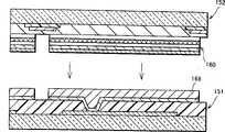
以下,如图8(a)所及图8(b)所示,将形成了有机EL元件的对向基板52与TFT基板51相互对准,贴合固定,在此,有机EL元件60利用导电接触层66TFT与基板51电气连接,理想地,TFT基板51和对向基板52上都事先涂好导电性树脂,使得导电性树脂双方电气接触良好,防止因金属表面氧化膜造成的接触不良,要利用树脂所具有的弹性可以容易实现接触。Hereinafter, as shown in FIG. 8(a) and FIG. 8(b), the
然后,注入液晶。注入是在TFT基板51与对向基板52相互贴合以后,并可以用真空注入法注入。Then, liquid crystal is injected. Implantation is performed after the
接着对有机EL元件60所用各种部件的材质等加以说明。Next, materials and the like of various components used in the
首先,有机EL元件用白色发光的发光层63液晶显示元件20中显示要用的彩色滤色层28要照其原样使用,但也来必限于这一种,也可用友红(R)、绿(G)、兰(B)中任何一种质色光的发光层63,这时,彩色滤包层28的部分要做成透明。First of all, the
也就是说,发光层63的发光,根据红(R)、绿(G)、兰(B)各种颜色其发光亮度的时效劣化不同,因此,把发光层63用于显示元件中时,随着时间的过去色平衡将会崩溃,这一点采用发白色光的发光层63时可以防止这种时效性的色平衡劣化。但另一方面,用发白色光的发光层63的同时,使用各种颜色的彩色滤包层28的情况下。根据各色彩色滤色层28的不同,透过率成为1/3,所以,结果是光利用效率降低。That is to say, the luminescence of the
因此,任何情况都是辨证的,与考虑到使用期间较短的显示和正确的色平衡相比,还不如重视亮度的显示理想的为采用红(R)、绿(G)、兰(B)各种颜色的发光层63,而对有长时时彩色平衡要求的如电视等用理想的为灰白色的发光层63。Therefore, any situation is dialectical, and it is better to pay attention to brightness than a display with a short period of use and correct color balance. The ideal display is to use red (R), green (G), blue (B) The
下面,例举能作为由发各色光的低分子型发光材料组成的发光层63用的材料,萘、葸、菲、芘、并四苯、荧光素、芘酞二萘嵌苯、萘酞芘、二萘嵌苯、二二苯丁二烯、四苯基十二烯、香豆素、氮萘金属络化物、亚胺、二苯葸、二氨基唑、芥子喹因、勒布朗等。Below, examples of materials that can be used for the light-emitting
另一方面,作为发白光的发光层63的材料可例举有,兰色金属络化物(Znboxz:Zinc-benzoxyazolz)和黄色金属络化物(Znsq2:Zinc-styrylquinoline2)。也可将荧光色素芘,DCM1(4-(Dicyanemethylent)-2-methy1-6-(4-dimethylaminostyry1)-4H-pyran)掺杂在其中使用。在聚合材料的叠层、聚乙烯咔唑上使用将PBD(2-(4-Biphenyly1)-5-(4-tert-buthlpheny1)-1.3.4-oxadiazol)分散后的单层材料。On the other hand, examples of materials for the white
另外,用作空穴输送层64的材料有,酞化菁化合物、蔡酞化菁化合物、初卟啉类、三唑、咪唑、四氢味唑、恶唑、芪子。In addition, materials used for the
还有,作电子输送层62的材料有,萄酮、葸醌基地多威,二苯基对苯醌、四唑、二蔡嵌苯羰基酸。Also, materials for the
阴极61的电极材料可例举如下,铝(Al)、镁(Mg)、银(Ag),还有将镍(Ni)、钛(Ti)、钽(Ta)、金(Au)等,金属材料重叠在上述材料之上,可提高接触性能。The electrode material of the
再有,作为用于TFT基板51与对向基板52接合的导电性接触层66的连接导电性树脂,例如,特开平11-249299号公报中所记载的导电粒子分散感光树脂(富士胶片株式会社制)、杂志1986 The Chemical Society of Japan的“Chemistry letters,pp.469472,1986”中所记载的能利用聚吡咯组成的感光导电聚合物。更详细的,在特开平11-249299号公报中有关碳黑等导电性粒子被分散的感光性分散物及感光的技术,用曝光及显像来形成布线图案等已公开的论文。另外在“Chemistry Letters,PP.469-472,1986”中公开使吡咯单体光化学聚合,使带导电性,形成聚吡咯,作为电极材料也公开了制作布线图案所使用的。In addition, as the connection conductive resin used for the
以下对有关对向基板52上形成的相差片31及偏振片32的特性作一叙述。The characteristics of the
这一些相差片31及偏振片32在液晶显示元件20上,为了构成除了特定的液晶方式的反射型液晶显示装置,要除去特定的液晶方式,这种情况下,相差片31通常是1/4波长,在本实施形态中,对于有机EL元件60的阴极61,为了提高反射效果,可使用铝(Al)等金属,因此,有机EL元件60的非发光时,用阴极61进行光反射,对比度会下降。因此,通常为了防止反射,在有机EL元件60的显示面一侧必须要偏振片32及1/4波长的相差片31,这一点,在本实施形态中,在反射型液晶显示元件20中,由于预先准备好相同结构的偏振片32和相差片31,可以不必重新设置而能够共用。These
以下,对具备所述结构的显示装置50的驱动电路在图9的基础上作一说明。本驱动电路中,应有效地驱动作为形成矩阵状显示区的各显示像素,共用有关液晶显示元件20及有机EL元件60的驱动的作为信号线及扫描信号线的控制总线3…、作为信号线及数据信号线的源极总线2a…。但本发明中未必限于这样,也可以适用于单纯的矩阵,另外,关于驱动回路详细情况请参见实施形态7。Hereinafter, the driving circuit of the
如该图所示,在显示装置50中的一个像素的电路结构中,液晶用TFT元件22的控制极电极与控制极总线3相连,源极总线2a与液晶用TFT元件22的源极接续。另外,液晶用TFT元件22的漏极22a与液晶显示元件20、液晶辅助容量35、EL用TFT元件42的控制极电极连接。又,EL用TFT元件42的漏极与有机EL元件60的阴极61连接。又,在上述构造中,有机EL元件60设置在EL用TFT元件42的漏极侧,但未必仅限于此,例如,如图10中所示,也可设在EL用TFT元件42的源极侧。As shown in the figure, in the circuit structure of one pixel in the
这样结构的显示装置50的驱动电路,用输入到控制极总线3…的扫描线信号Vg控制液晶用TFT元件22通/断,将源极总线2a…的数据线信号Vs输入液晶显示元件20,液晶显示元件20的灯亮状态由液晶辅助容量35来确保。又,本实施形态中,EL用TFT元件42的EL用阈值电压Vth(OLED)设定得比液晶显示元件20的动作范围电压更高,即,源极总线2a…的数据线信号Vs的电压一旦超过液晶显示元件20的驱动电压范围,液晶显示元件20饱和,另一方面,EL用TFT元件42处于导通状态,有机EL元件的发光。The driving circuit of the
另一方面,液晶显示元件20设定于正常时白色模式、饱和状态时为黑色,因此,有机EL元件60发光的电压范围时,液晶显示元件20成为有机EL元件60的黑色矩阵由于液晶显示元件20,对比度不会变低。On the other hand, the liquid
又,光耗液晶显示元件20动作的范围而言,发光区12a不发光,由于设于显示屏面的偏振片32及相差片31成为黑的状态。因此有机EL元件60的液晶显示元件20的对比度不会变低。Also, in the range where the light-consuming liquid
具体地说,如图11所示,数据线信号Vs未满EL用TFT元件42的EL用阈值电压Vth(OLED)时,有机EL元件60不发光,液晶显示元件20起反应,从亮显示到暗显示,即进行黑的显示。Specifically, as shown in FIG. 11, when the data line signal Vs is less than the EL threshold voltage Vth (OLED) of the
又,数据线信号Vs比EL用TFT元件42的EL用阈值电压Vth(OLED)大时,液晶显示元件20进行暗显示,根据数据线信号Vs,EL用TFT元年42的漏电流变化。调节有机EL元件60的发光量,作发光型显示,再者,有机EL元件60的发光量的调节也能通过对供电电压Vdd的调节来进行,另外,本实施形态的显示装置50,其驱动方法没有限定,也可以用其他驱动方法,图11中所示的驱动方法其驱动电路是共用的,因此最佳。Also, when the data line signal Vs is higher than the EL threshold voltage Vth(OLED) of the
一方面,作为与所述的驱动方法不同的驱动方法,在所述有机EL元件60及液晶显示元件20双方的显示不能作到一体化的情况下,驱动电路最好设置成能各自独立驱动的方式,这样,液晶显示装置20设定为正常时黑色、液晶显示元件20处于截止状态下为黑色,这是因为液晶显示元件20在不工作时,利用液晶显示元件20不会无谓地消耗电力也有助于提高显示的对比度。On the one hand, as a driving method different from the above-mentioned driving method, in the case where the display of both the
再者,对于以往的将透过型液晶显示元件与反射型液晶显示元件组合在一起的液晶显示装置,必需有透过型显示用光源及其所用电源,而在本实施形态的显示装置50中,是将有机EL元件60和反射型的液晶显示元件20组合安装在同一屏板内,如果,预先让驱动部备有电源,则能进行亮度的调节。Furthermore, for conventional liquid crystal display devices that combine transmissive liquid crystal display elements and reflective liquid crystal display elements, it is necessary to have a transmissive display light source and a power source for it, and in the
因此,本实施形态的显示装置50,不需要光源用的电源能够做到降低成本,减少部件、小型化。又,为使信号布线共用化,则利用信号布线上的电压切换发光显示的元件和利用外光进行显示的非发光显示元件时,如所述图2中所示,自发光亮度在某一点W上降到0的情况相当。Therefore, the
就这样,对于本实施形态的显示装置50,在各显示像素10…内一并设置有液晶显示元件20反射外来光进行显示的非发光显示元件形成的反射区11、以及有机EL元件60直接调制进行发光的发光显示元件形成的发光区12a。In this way, in the
因此,在一对绝缘性基板21及29之间一并装有液晶显示元件20及有机EL元件60,故显示装置量厚度可以减薄。Therefore, since the liquid
因此,有机EL元件60向着显示面一侧,自身发光直接显示,不是以往那样,将有机EL元件60作为背景灯和正面灯使用。因而,由此不仅来自有机EL元件60的光能够提高利用效率,而且显示装置的厚度也可减薄。也就是说,背景灯及正面灯的厚度通常是3~6mm左右,如不用背景灯,则对于厚度减薄很有好处,另外,不用背景灯意味着,不需要以往的设置在液晶屏的背面与背景灯之间的背面侧的偏振片、相差片及玻璃基板等。如此,显示装置的厚度可以更加薄。Therefore, the
进一步而言,不需要背景灯、背面侧的偏振片以及相差片的优点在于,不仅是显示装置整体厚度变薄,在减少部件数量上,不仅减少了材料费而且装配人工及各种零部件检查所需的成本也都能削减,从而显示装置整体制造成本将能下降。Furthermore, the advantage of not requiring a backlight, a polarizing plate on the back side, and a phase difference film is that not only the overall thickness of the display device is thinned, but also the number of parts is reduced, not only the material cost is reduced, but also assembly labor and various parts inspections are reduced. The required cost can also be reduced, so that the overall manufacturing cost of the display device can be reduced.
因此,在实现小型化、降低成本的同时,还能提供从野外到室内视觉识别性优越的显示装置50。Therefore, it is possible to provide the
又,本实施形态的显示装置50中,具有相互对向的绝缘性基板21及绝缘性基板29,液晶显示元件20及有机EL元件60任一个都设置在绝缘性基板21与绝缘性基板21的中间,因此,液晶显示元件20及有机EL元件60都收容在绝缘性基板21与绝缘性基21的中间,故显示装置50的厚度确实能够减少。In addition, in the
又,本实施形态的显示装置50中,其发光区12a内,液晶显示元件20的液晶层26不存在,即,有机EL元件60的发光层63的显示面一侧不存在液晶显示元件20的液晶层26,即从有机EL元件60向显示面方向出射的光不会通过液晶层26,意味着射向显示装置50以外。再者,假设在发光层63的显示面一侧不存在液晶层26,在本实施形态以外,例如实施形态3所示,液晶层26的显示面侧的端面存在于比发光层63的显示面侧的更靠显示面侧,但由于绝缘性凸起部81等绝缘层的存在,发光层63的显示面侧,即,有时发光区12a的液晶层26被排除,又,作为该以外的构造,能考虑到发光层63在液晶显示20的显示面侧上存在的类型。Also, in the
结果,有机EL元件60的出射光由于没有被液晶显示元件20的液晶层26散射或吸收,因此难于使亮度下降,并能使有机EL元件60的显示品质提高。As a result, since the emitted light of the
又,本实施形态的显示装置50中,液晶显示元件20的液晶层26与有机EL元件60的发光层63被设置在同一层面,而所谓同层,未必是指同一平面,包括有机EL元件60的发光层63被包含在液晶显示元件20的液晶层26的状态。Also, in the
因此,在以往的液晶显示元件20形成的非发光显示元件的厚度范围内能收容有机EL元件60。其结果能确实地减薄显示装置50的厚度。Therefore, the
又,本实施形态的显示装置50中,驱动有机EL元件60及液晶显示元件20的液晶用TFT元件22、以及EL用TFT元件等的驱动元件,形成在一方的TFT基板51侧,另一方面,在与该TFT基板51的对向的对向基板52侧形成有机EL元件60。Moreover, in the
由此,在制造显示装置50时,可以另外形成有机EL元件60、液晶用TFT元件22以及EL用TFT元件42等驱动元件,因此,当形成有机EL元件时,不会受到液晶用TFT元件22及EL用TFT元件42等的驱动元件形成时的工序温度、药品、气体等的影响。Thus, when manufacturing the
又,有机EL元件60的出射光射向对向的对向基板52侧,故不会被驱动有机EL元件60的EL用TFT元件42遮挡,能有效地利用光,并能从阳极65即透明导电层开始形成发光层63,籍此,能以与前同样结构形成发光层63。Again, the outgoing light of the
可是,在将有机EL元件60设置在与液晶显示元件20的液晶层26同一层时,并不限于有机EL元件60的形成高度要与液晶显示元件20的液晶层26的厚度一致。However, when the
关于这一点,本实施形态中在TFT基板51上设置导电接触层66,用于调整高度,在该导电接触层66上形成有机EL元件60。In this regard, in this embodiment, a
因而,能确实地把有机EL元件60设置在与液晶显示元件20液晶层26同一层上。Therefore, the
又,本实施形态的显示装置50中,导电接触层是用导电树脂制成的,因此,人TFT基板开始形成导电树脂形成的导电接触层66,因而,能容易地在TFT基板51侧上进行高度的调整。Also, in the
又,在本实施形态的显示装置50中,在有机EL元件60的阴极61与TET基板51侧的接合面上敷设有导电糊或导电树脂等的导电性材料。Further, in the
即,导电糊或导电树脂,通常即使硬化,仍具有柔软的弹性,因此,能使有机元件60的阴极61与TFT基板51侧可靠地电气接合。That is, the conductive paste or conductive resin usually has soft elasticity even when it is hardened, so that the
又,本实施形态的显示装置50中,有机EL元件60、液晶显示元件20共用源极总线2a…及控制极总线3…并进行驱动。Moreover, in the
因此,为了防止有机EL元件60和液晶显示元件20的驱动电路构成变得十分繁复,能够提供确实地减少显示装置厚度和部件成本的显示装置50。Therefore, in order to prevent the drive circuit configuration of the
又,本实施形态的显示装置50中,有机EL元件60及液晶显示元件20也做成彼此独立驱动,为了有机EL元件60及液晶显示元件20能实现单独的驱动,作为这样驱动用的一种结构,举例如下,有将有机EL元件60及液晶显示元件20各自具有源极总线2a及控制极总线3的情况,或将源极总线2分别设置而将控制总线3共用的情况。Moreover, in the
又,本实施形态的显示装置50中,将驱动有机EL元件60及液晶显示元件20的EL用TFT元件22在一方的基板即TFT基板51上形成,因此通过TFT基板51上形成EL用TFT元件42及液晶用TFT元件22能使显示装置50的制造更为容易并避免构成复杂。Moreover, in the
又,本实施形态的显示装置50中,光调制元件是反射型的液晶显示元件20,发光元件是有机EL元件60,因此,通过将反射型的液晶显示元件20及有机EL元件一并设置于各显示像素10内。In addition, in the
结果,确实能小型化和降低造价,同时也提供了野外和室内都适用,视觉识别性优越的显示装置50。As a result, the
又,本实施形态的显示装置50中,液晶显示元件20的对向电极27与有机EL元件60的阳极65是用同一种材料并在同一层上形成,因此,使制造工艺共用,制造过程简单。Also, in the
又,本实施形态的显示装置50的制造方法中,在一方的基板上即TFT上,形成液晶用TFT元件22及EL用TFT元件42,在另一方的基板上即对向基板52上,形成有机EL元件60后,通过将这些TFT基板51及对向基板52相互合拢形成一体。In addition, in the manufacturing method of the
在制作显示装置50时,有机EL元件60、液晶用TFT元件22以及EL用TFT元件42也可另行形成,因此,在形成有机EL元件60时,就能不受液晶TFT元件22及EL用TFT元件42形成时的工序温度、药品、气体等的影响。When manufacturing the
结果,能提供一种不但可实现小型化以及降低成本而且从野外到室内视觉识别性优良的显示装置的制造方法。As a result, it is possible to provide a method of manufacturing a display device that not only achieves miniaturization and cost reduction but also has excellent visibility from outdoors to indoors.
又,在本实施形态的显示装置50的制造方法中,可以先形成有机EL元件60及芯部77、77中的任意一个。因此,能够使得可容易地形成有机EL元件60与芯部77、77的工序优先进行。In addition, in the method of manufacturing the
又,本实施形态的显示装置50中,在有机EL元件60的阴极61与TFT基板51侧的接合面上,设置导电糊或导电树脂以后明TFT基板51与对向基板52贴合。Furthermore, in the
为此,使得将有机EL元件60的阴极61与TFT基板51的接合面为树脂和树脂、或树脂与树脂糊,利用通过树脂相互之间以及树脂糊的弹力,使接合性能提高。For this reason, the bonding surface between the
实施形态2
参见图12~图15,以此为基础,对本发明的其他实施形态,说明如下,为便于说明,凡在所述实施形态1的示图中表示过的部件或具有同一功能的部件,赋以同一符合并省去说明。Referring to Fig. 12~Fig. 15, based on this, other embodiments of the present invention are described as follows, for the convenience of description, all the parts shown in the diagrams of the first embodiment or the parts with the same function are assigned with The same match and omit description.
本实施形态中,对于以高分子型EL材料制造有机EL元件的情况进行说明。In this embodiment, a case where an organic EL element is produced using a polymer EL material will be described.
本实施形态的有机EL元件70,如图12所示,发光层73用高分子型EL材料,该发光层73的上下直接与阴极61及阳极65相接,即,本实施形态有机EL元件70省略了所述实施形态1中的有机EL元件60中存在的空穴输送层64及电子输送层62,但是本实施形态也可以设置这些空穴输送层64及电子输送层62。The
另外,本实施形态中发光层73的两侧形成为了与液晶层26相绝缘的、作为保护层的芯部77、77。又,在形成发光层73时,首先形成芯部77、77,将EL材料喷射涂布或印刷在它们内部而形成发光层73。In addition, in the present embodiment,
所述芯部77、77可采用抗蚀剂、聚酰亚胺等制作。又,芯部77、77最好是遮光性的材料,这是因为从散光层73出射的光其向横方向的漏光会进入液晶层26而形成眩光,导致对比度低下。The
所述有机EL元件70的制造方法说明如下。The method of manufacturing the
首先,如图13(a)所示,在对向基板52的对向电极27及阳极65侧形成芯部77、77。这是采用抗蚀剂或聚酰亚胺并以光致蚀刻、喷射涂布工艺形成。First, as shown in FIG. 13( a ),
然后,如图13(b)所示,在该部分例如用喷墨涂布方式形成了高分子型EL材料的散光层73,作为高分子型EL材料可用,聚苯撑乙烯、多氟纶、多噻粉、聚乙烯咔唑等。Then, as shown in FIG. 13( b), a light-
最后,如图13(C)所示,例如也可将导电性高分子材料涂布在这上面形成阴极,也可(未图示)用铝(Al)、镁(Mg)、铝-镁(Al-Mg)合金等金属材料,形成金属糊后涂布高分子材料,用作阴极61。Finally, as shown in FIG. 13(C), for example, a conductive polymer material can be coated on it to form a cathode, and aluminum (Al), magnesium (Mg), aluminum-magnesium ( Metal materials such as Al—Mg) alloys are formed into a metal paste and then coated with a polymer material to be used as the
另一方面,TFT基板51侧如图14所示,在形成了液晶用TFT元件22、EL用TFT元件42及像素电极25的TFT基极51上,将感光导电树脂以喷墨涂布方式进行涂布,形成导电接触层66。然后,如图15(a)及图15(b)所示,形成导电接触层66。然后,如图15(a)及图15(b)所示,形成有机EL元件70的对向基板52,与TFT基板51相互对准,与所述实施形态一样,进行贴合、固定、最后注入液晶、封装。On the other hand, on the
此后,注入液晶并进行封装。这时,形成的芯部77、77在扫描线的方向,在整个显示屏宽度上形成的情况下,可以从显示屏的端面起,沿着扫描线进行真空注入。Thereafter, liquid crystal is injected and encapsulated. At this time, when the
又,其他结构以及该有机EL元件70的驱动动作、显示方法等与实施形态1相同,并省略说明。The rest of the structure, the driving operation of the
这样地,本实施形态的EL元件70,至少由发光层73、与形成在该发光层73两侧的阴极61及阳极65所构成。In this way, the
因此,例如,在形成由高分子型EL材料制成的发光层73时,能由最小限度构成要素形成有机EL元件70。Therefore, for example, when forming the
然而,所述的显示装置50中,有机EL元件70因与液晶显示元件20的液晶层26同层设置,液晶显示元件20的液晶层26与有机EL元件60之间可能相互影响,例如,有机EL元件70的缘故,液晶显示元件20的液晶等的液晶层与有机EL元件70发生接触,就会引起双方的性能下降,材料劣化。另外,有机EL元件70有时也会因与空气和水分接触的劣化。However, in the
然而,在本实施形态中,有机EL元件70的发光层73与液晶显示元件20的液晶层26是通过芯部77、77而连接着。However, in the present embodiment, the
因此,可以防止有机EL元件70的发光层73与液晶显示元件20的液晶层26相互影响。即,将有机EL元件70与液晶显示元件20的液晶层26设置在同一层之后,双方的性能会下降,但却能防止材料劣化,另外在显示装置的制造过程中,例如在对向基板52侧上形成有机EL元件70时,由于发光层73受到芯部77、77及阴极61的保护,防止发光层73与空气和水分接触而劣化。Therefore, it is possible to prevent the
但是,也考虑到从有机EL元件70发出光漏向邻接的液晶显示元件20的情况。However, it is also conceivable that light emitted from the
在这一点上,本实施形态的显示装置50中,因为芯部77、77具有遮光功能,能防止有机EL元件70所发的光漏向液晶显示元件20的液晶层26。In this regard, in the
[实施形态3][Embodiment 3]
本发明的其他发明形态,参见图16~图19并说明为下,为便于说明凡在上述实施形态1及实施形态2中说明过的或具有相同功能的元件赋以同样的符号,其说明省略。Other inventions of the present invention are described below with reference to FIGS. 16 to 19 . For the convenience of description, the components that have been described in the first embodiment and the second embodiment or have the same functions are given the same symbols, and their descriptions are omitted. .
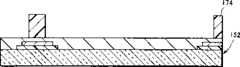
本实施形态的显示装置50,为图16所示,在对向机板52一侧上设置有硬质、透明的绝缘凸部81,另将有机EL元件70设置在TFT基板51的侧。上述绝缘性凸部81是作为液晶层26的厚度控制用的支柱使用的。The
即,液晶层26的厚度通常大多设定为3~5μm,另一方面,有机EL元件70的厚度是0.1~0.5μm左右,在上述的实施形态1及实施形态2所示的图1~图12中,对于有机EL元件50及有机EL元件70,其厚度差通过连接树脂即导电接触层66进行调整。That is, the thickness of the
对此,在本实施形态中,设有预先考虑了液晶层26和有机EL元件70的厚度差的绝缘性凸部81。厚度差在图16中虽没有明示,但其存在于接续部。On the contrary, in this embodiment, the insulating convex portion 81 is provided in which the difference in thickness between the
作为形成所述绝缘性凸部81的材料要使用高透过率树脂,例如可使用JSR株式会社制造的感光隔离材料,制品名称OPUTOMA-NN系列,该高透过率树脂比所述导电接触层66及连接部所用连接树脂形成后的硬度高,利用这性质通过设定高度,可以期待使对向基板52和TFT基板51的间距保持一定的效果。As the material for forming the insulating convex portion 81, high transmittance resin will be used. For example, the photosensitive isolation material manufactured by JSR Co., Ltd., the product name OPUTOMA-NN series can be used. The high transmittance resin is higher than the conductive contact layer. 66 and the connection resin used for the connection portion have high hardness after formation, and by setting the height by utilizing this property, the effect of keeping the distance between the
以往,液晶层26的厚度是依靠散布于该液晶层26中的隔离珠来进行控制,而因为在液晶层26的像素显示面会导致对比度下降和散射,引起图像品质量变差,另外,依靠隔离珠的方法还是不能的充分地控制厚度。In the past, the thickness of the
但,在本实施形态中利用上述绝缘凸部81进行的厚度控制,液晶层26的厚度控制精度提高的同时,也能够期待提高显示屏的强度。However, in the present embodiment, the thickness control by the above-mentioned insulating protrusions 81 improves the thickness control accuracy of the
又,本实施形态中,绝缘凸81不仅为了上述的厚度控制而用,并不限于此,将此绝缘凸部81用作有机EL元件70的光控器材,即,可作控制有机EL元件70发出的光的光学元件来使用,为了此目的,例如,如图17所示,可以为由锯齿状凸部82a、82b组成的绝缘凸部82,锯齿状凸部82a,82b为将不同折射率的多个透明树脂做成两层锯齿状的凸部。利用这样的构造,能使有机EL元件70发射的光带有方向性,又,改变锯齿形状可使指向特性相应变化,所以就可能得到与液晶显示装置同样的视野角特性。Also, in this embodiment, the insulating protrusion 81 is not only used for the above-mentioned thickness control, but is not limited thereto. The insulating protrusion 81 is used as a light control device for the
因此,从显示面来看本实施形态的有机EL元件70时,如图18所示,由长宽决定的范围相当于一个显示像素10…,并且分割成各个反射区11和发光区12a。又,同该图所示,对于各反射区11和发光区12a,连接像素电极25与液晶用TFT元件22或EL用TFT元件42的通孔25a。Therefore, when the
又,所述显示像素10…上反射区11及发光区12a,的分割配置并必仅限于此,例如图19所示,如有机EL元件70形成的发光区12a被包围在由液晶显示元件20形成的反射区11中,反射区11与发射区12a中的任何一方可被另一方包围,该图所显示的由有机EL元件70形成的发光区12a被包围在液晶显示元件20形成反射区11之中的形状,有机EL元件70发光时,假设同围的液晶显示元件20的反射区全部为黑,则相邻接的显示元件作黑色矩阵作用,因此与所述图18的形状比较,对提高对比度有效。Also, the division configuration of the
又,如图19(b)中所示的形状,显示像素被敷满的话,有机EL元件80的发光区12a被围在由液晶显示元件20的反射区中可以期望得到同样的效果。19 (b) shown in the shape, if the display pixels are filled, the
又,关于发光区12a和反射区11的面积可根据显示装置用途来定。In addition, the areas of the light-emitting
又,本实施形态中,关于由高分子型EL材料组成的发光层73的有机EL元件70已经作了说明,但并不限于此,对于低分子型EL材料组成的发光层63的有机EL元件60也可能同样适用本实施形态。Also, in the present embodiment, the
又,关于其他的构成,与所述实施形态1至实施形态2相同,故不再说明。In addition, other configurations are the same as those of
如此,本实施形态的显示装置50中,在对向基板上形成调整高度用的绝缘凸部81或绝缘凸部82,同时,该绝缘凸部81或绝缘82上形成有机EL元件70。In this way, in the
因此,将有机EL元件70与液晶显示元件20的液晶层26设置同一层的情况下,即使有机EL元件70的高度与液晶显示元件20的液晶层26的厚度不相一致,也可以可靠地将有机EL元件70与液晶显示元件20的液晶层26设置在同一层。Therefore, when the
又,本实施形态的显示装置50中,绝缘凸部82由硬度绝缘层形成,因此,通过在对向基板52的一侧形成由绝缘层形成的绝缘凸部81或绝缘凸部82,可以容易地从对向基板52的一侧调整高度,另外,绝缘凸部82是用硬质绝缘层形成的,因此,能使液晶显示元件20的液晶层26的间隔保持一定,并起到隔离的作用。In addition, in the
又,本实施形态中,将硬质绝缘层形成的绝缘凸部82制成两层,并将其界面形成锯齿状为锯齿状凸部82a、82b,借助这样的方法可使有机EL元件60出射的光具有方向性,这样能使绝缘凸部82作为有机EL元件60的光控部件发挥其功能。Also, in this embodiment, the insulating convex portion 82 formed by the hard insulating layer is made into two layers, and the interface thereof is formed into sawtooth-shaped convex portions 82a, 82b. By such a method, the
又,本实施形态的像素分割式显示装置50中,能够任意地设定反相区11和发光区12a的比率,例为使用于于手机携带或信息移动终端(PDA)等移动通信设备的场合下,反射区即通常使反射领区11所占的比率增大,一般在显示像素10的像素面积中80%是反射区的场合时,发光区12a是20%,因此,有机EL元件60的发光面积最大也只是像素面积的五分之一。In addition, in the pixel-divided
因此,能够提供一种小型、廉价而且不论野外或室内都具有优越视觉识别性的显示装置。Therefore, it is possible to provide a display device that is small, inexpensive, and has excellent visibility both outdoors and indoors.
又,本实施形态的显示装置50中,液晶显示元件在亮显示状态时,有机EL元件70可以选择不发光的状态,这是因为亮环境使用时,有机EL元件70处于不发光状态,由于仅让液晶显示元件20进行显示,这样,可以防止有机EL元件70劣化、延长其寿命,同时节省电力清耗。Moreover, in the
又,本实施形态的显示装置50中,液晶显示元件20及有机EL元件70被安排相邻的位置,因此,液晶显示元件20及有机EL元件70的任意一方在亮显示状态时另外一方则处于暗显示状态中。这样一来,总有一方成为黑色矩阵,在显示上就不会降低对比度。Also, in the
实施形态4
本发明的其他实施形态,以图20为基础进行说明。又,为便于说明,对在所述实施形态,到实施形态3的附图上已经出现过的或具有同一功能的部件注上相同符号,不再说明,因时在实施形态1至实施形态3中已叙述过的各种特征,本实施形态中也同样适用。Another embodiment of the present invention will be described based on FIG. 20 . Again, for the convenience of description, in the above-mentioned embodiment, the components that have appeared on the drawings of the third embodiment or have the same function are marked with the same symbols, and will not be described again. The various features described above are also applicable to this embodiment.
本实施形态中将对利用光传感器检测外来光线,根据其检测结果调节有机EL元件60或有机EL元件70亮度的情况进行说明。In this embodiment, a case will be described in which external light is detected by an optical sensor, and the brightness of the
即,为图20所示,显示装置50中设有作为显示控制手段的控制电路91及测量电路92,该控制电路91收到图像显示的信号后,通过电源部90向源驱动器6发出信号,同时,向门控驱动器7发出信号,在本实施形态中,通过测定电路23,作为外光检测手段的光传感器93被接在控制电路91上。That is, as shown in FIG. 20, the
然后,控制电路91进行光传感器93的控制和外光测定的控制,光传感器93可由例如光敏晶体管元件等构成。Then, the control circuit 91 performs the control of the photosensor 93 and the control of external light measurement, and the photosensor 93 can be constituted by, for example, a phototransistor element or the like.
又,本实施形态中,作为发光元件使用有机EL元件60及有机EL元件70的同时,也使用作为光调制元件的液晶显示元件20,所述电源部90假设为与液晶驱动相比更需要驱动能力的有机EL元件60或有机EL元件80的驱动用恒电流或恒电压电流。因此,作液晶显示时,不用电源部90。In addition, in this embodiment, the
下面,对根据所述光传感器93进行控制和外部光测定的控制器作一说明。Next, a controller for controlling and measuring external light based on the optical sensor 93 will be described.
首先,在暗环境下,控制电路91根据来自光传感器93的信号识别周围为暗环境的情况,并产生驱动有机EL元件60及有机EL70的数据信号和门控信号,这样,有机EL元件60或有机EL元件70的灰色等级显示在电流部90一侧进行的场合下,从控制电路91将信号送往电源部90。First, in a dark environment, the control circuit 91 recognizes that the surrounding is a dark environment according to the signal from the light sensor 93, and generates data signals and gate signals for driving the
另一主面,亮环境时,根据光器发来的信号,产生驱动反射型液晶显示元件20的数据线路2主号及门控线信号,这时为前所述,因和电源部90没有关系,从控制电路91直接控制电源的信号。On the other main surface, when the environment is bright, according to the signal sent by the optical device, the
在要使用机EL元件60或者有机EL元件70与液晶显示元件双方同时显示时,从电路91发出各显示用源信号,藉此,各显示总能进行亮度调整,能根据周围的环境选择最清的显示状态。When both the
这样,不仅借助于利用光敏元件93对外部光测定,不仅能自动地让有机EL元件60或有机EL元件70发光或让液晶显示元件20进行反射显示的交替切换而且能选择最适合于环境状态。In this way, not only can the
以上所述,本实施诉显示装置50,借助控制电路91,在由光敏感无件进行外部光测定结果的基础上,能选择显示有机EL元件60或有机EL元件70及液晶显示元件20的双方或其中任意一方。As mentioned above, the
因此,可以根据周围的亮暗程度,自动选择有机EL元件60、有机EL元件70或液晶显示元件20的显示,以确保最佳的显示状态。Therefore, the display of the
实施形态5Embodiment 5
本发明的另外实施形态,以图21~图26为基础说明为下。Another embodiment of the present invention will be described below on the basis of FIGS. 21 to 26 .
为便于说明,凡在前述的实施1~实施形态4的附图中出过的部件或具有相同机能的部件均标以相同的符号,并省略说明。又,在前述实施形态1~实施形态4已叙述过的各种特征,在本实施形态中同样适用。For the convenience of explanation, the same reference numerals are assigned to the parts shown in the drawings of the first to fourth embodiments or the parts with the same functions, and the description thereof will be omitted. In addition, the various features described in the aforementioned first to fourth embodiments are also applicable to this embodiment.
本实施诉显示装置1如图21所示,利用在纵向上设有的多根作为数据信号线的源极总线2a…、横方向上设有的多根作为扫描信号线的门控总线3…,使作为显示区的各显示像素10…形成为矩阵状。The
在本实施形态中,所述显示像素10分割为由具有反射性的第1显示区即反射区11、具有透过性的第2显示区即透过区12。如图22所示,所述反射区11是由构成作为光调制元件的反射型液晶显示无件20的铝(Al)等金属组成的像素电极25形成,由此,外部光4被这些像素电板25反射。In the present embodiment, the
另一方面,如该图所示,在像素电极25的中央部位有一个形开口部25,此开口部形成了上述的透过区12。在像素电极25的开口部25a的下方,即在像素电极25的后方通过透明绝缘层24设有作为发光元件的有机EL元件40,此有机EL元件40依靠自身发出的显示光5直接进行显示,即,本实施形态不是以往那样也将有机EL元件当作背景灯光或前照光使用,有机EL元件40能直接进行显示,因而本实施形态的显示装置1可以说是将液晶显示元件20构成的反型液晶显示装置与有机EL元件40构成的有机EL显示装置做成一体的显示装置。On the other hand, as shown in the figure, there is a
这里,所述的有机EL元件40可能与透过区12的面积大致相等或比它小一些,即,有机EL元件40不必在整个透过区12上形成而可根据面画亮度形成所需的面积,因此,把有机EL元件40的面积做成比透过区12小,还可使有机EL元素40消耗的电力降低。又,如果把有机EL元件40做的与透过区12基本相同创意味着有机EL元件40比透过区12的面积稍大的也可以即,有机EL元件40比透过区12的面积仅稍大的一时,有机EL元件40的照射效率是无妨的,另外,即若有机EL元件40比透过区12的面积稍大,像素电极25发挥黑色矩阵的作用,所以不会引起问题。Here, the
上述显示装置1如图一所示,在作为玻璃基板等的第一基板的绝缘基板21上设有液晶用TFT元件22。此液晶用TFT元件22如图21所示,它与所述门控总线3…及源板总线2a…连接,并且是作为通过漏极要板22将电压施加于像素电极25的开关元件发挥功能。In the
另一方面,所述液晶显示元件20的漏电极22a如该图所示,与用来驱动机有EL元件40的EL用TFT元件42的控制电极42a连接,又,此EL用TFT元件42的源极侧上与供电线2b连接,EL用TFT元件42导通时,由于有供电电压Vdd,使供电线2b通过EL用TFT元件42的漏电极42a,有机EL元件40的有机EL层41上驱动电流流过且有机EL层41发光,又,有机EL层41在具有所述的低分子型EL材料的发光层63的有机EL元件60上,由电子输送层62、发光层63、空穴输送层64构成,另外,对于具有所述的高分子型EL材料的发光层73,仅由发光层73构成。On the other hand, the
这里根据图21及图22对所述显示装置1的结构的制造方法进一步作更详细的说明,Here, the manufacturing method of the structure of the
首先,如图21所示,在玻璃基板等绝缘基板21上形成液晶用TFT元件22,这时,EL用TFT元件42也在同时形成。接着,用感光性的丙烯树脂将平面膜23例为形成2μm厚,此后,将构成有机EL元件40的反射性阳极43用溅射法形成2000厚的铬(Cr)层,然后用溅镀法形成2000的二氧化硅(SiO2)层,然后经蚀刻形成规定图案的绝缘层44。接着,用蒸镀法形成发光层即有机EL层41,有机EL层41是用掩模蒸镀法将红、绿、蓝等发光材料对应着各种表示像素10…而形成,接着为了使得电子有效注入有机EL层41,用蒸镀法将镁、银等图中未示出的合金,形成100厚镀层及作为具有透明性的阴极45,再用溅镀法将铟一锌的氧化物(IZO)形成2000厚的层,再用溅镀法将五氧化二钽(Ta2O5)形成7000厚的透明绝缘层24,然后将驱动构成液晶显示元件20的液晶层26用的、具有反射性的液晶层26以铝形成。First, as shown in FIG. 21, the
另一方面,在其他玻璃基板等作为透明的第2基板的绝缘基板29上,顺次形成滤色层、铟一锡氧化物(ITO)组成的对向电极27。On the other hand, a color filter layer and a
接着,将液晶分子对着绝缘基板29,把有垂直取向性质的(未图示)取向膜(商品名[JALS204日本全成橡胶社制])用旋转涂布法涂布后再经过培烧形成。Next, the liquid crystal molecules are placed against the insulating
然后,通过形成开口部的图中未示出的掩膜,仅使形成有机EL元件40的部分以外的部分曝光,用紫外光照射绝缘基板31侧的成形基板,另一方面,即使对绝缘基板29侧的成形基板,在与绝缘基板21贴合的场合下,与有机EL元件40对向的部分以外的区上也要用紫外光照射,将该两枚成型基板加以摩擦,并对图中未示出的取向膜施以一轴取向处理,通过密封树脂贴合后,电介质各向异性为正时,将Δn0.06的液晶材料(メルク公司制)注入,制成液晶显示元件20。接着,将位相差板31与偏振片32依次贴附在绝缘基板29的表面上,由此完成显示装置1的制造。再有,相差片31的相位差,对λ=550nm的光,采用λ/4的相位差。Then, only the part other than the part where the
在将如此制成的显示装置置于外部光4中并不施加电压的状态下进行观察,有机EL元件40的上部位置上为黑显示,没有形成有机EL元件40的上部位置上为黑显示,没有形成有机EL元件40的部分呈白显示,这是由于经紫外光照射过的部分,发现取向膜的垂直取向性的官能基被切断,液晶分子对绝缘基板21及绝缘基板29平行取向。When the thus produced display device was placed in the
对该结果,液晶怪26的显示模式是在未施加电压时显示白色,电压施加后,反射率慢慢减少,呈现为进行黑显示的正常的白模式。As a result, the display mode of the
然后,以驱动所述结构的显示装置1用的驱动电路为例说明为下。Next, a driving circuit for driving the
如图23所示,显示装置1中,用来顺次传送数据线信号的源极驱动器6连接在源总线2a上,选择显示像素10…的门控驱动器7,连接于门控总线3…。又,一个显示像素10内的显示电路由光调制元件即液晶显示元件20以及发光元件即有机EL元件40构成。As shown in FIG. 23, in the
这些液晶显示元件20及有机EL元件40在各自显示装置1的显示区中排列成矩阵状,液晶显示元件20的对向电极27、EL用TFT元件42的供电线26及有机EL元件40的阴极45分别共通地连接于各液晶示元件20及有机EL元件40。即,该驱动电能中,用于将形成阵列状的作为显示区的各显示像素10…进行有源驱动的液晶显示元件20及有机EL元件40的驱动,信号线及扫描信号线即门控总线3…以及信号线和数据信号线即源极总线2a…等共用。但本发明未必仅限于此,也能适用于简单的矩阵。These liquid
结果是驱动该显示装置1时,也能够采用所述实施形态1的图9、图10及图11中的驱动方法。又,其驱动方法的详细说明同前述相同,故这里省略。As a result, the driving method shown in FIGS. 9 , 10 and 11 of the first embodiment can also be used for driving the
关于所述显示动作,根据图24~图26详细说明。再者,图24~图26中,记载了反射率最高条件下液晶层26不加电压时多折射为λ/4时光的状态。The display operation will be described in detail with reference to FIGS. 24 to 26 . Furthermore, in FIGS. 24 to 26 , the state of the multi-refraction of light at λ/4 is described when no voltage is applied to the
首先,在外部光4照射下使用显示装置1的场合下,在数据线信号Vs上无电压施加时或者液晶用TFT零件22的漏电压Vd未满液晶用阈值电压Vth(LC)时,以图24所示,外部光4在透过偏振片32及相差片31以后成为圆偏振光而向液晶层26射入。接着,由于液晶层26具有λ/4相位差,当到达反射性像素电极25时,相位差成为λ/2,外光4作为线偏振光来反射,反射后经过与入射时相反的路径,成线偏振光,所以透过偏振片32后成为白显示。这时,液晶用TFT元件22的漏电压Vd在EL用TFT元件42动作的EL用阈值电Vth(OLED)以下,因此,对有机EL元件40不供给电流,处于非发光状态中。First, when the
接着,在外部光照射下使用显示装置1,对施加比液晶用阈值电压Vth大的液晶用TFT元件22的漏电压Vd时液晶显示元件20为黑显示的情况进行说明。Next, a case where the liquid
参见图25,液晶层26的多次折射大致为零。因此,外光到达反射性的像素电极25的时刻例如是保持在右圆偏振的圆偏振光的状态,反射后的时刻例如成为左圆偏振光的逆向旋转的圆偏振光,因此,外部光4的反射光透过相差片41形成为与偏振片32的透过轴成90度垂直角的线偏振光。所以外部光4的反射光不能够透过偏振片32,显示成黑色。Referring to FIG. 25, the multiple refraction of the
又,这时,液晶用TFT元件22的漏极电压Vd未满EL用TFT元件42动作的EL用阈值电压Vth(OLED),故没有向有机EL元件40提供电流而保持在非发光状态。At this time, since the drain voltage Vd of the liquid
下面,对外部光4的强度减弱时,对于有机EL元件40发光的情况进行说明。Next, a case where the
如图26所示,使液晶用TFT元件22的漏电压Vd为EL用TFT元件42动作的EL阈值电压Vth(OLED)以上。这样,对有机EL元件40供电而发光。这时如图11所示,漏电压Vd足够高,液晶层26成为黑显示,不会影响有机EL元件40的发光度。As shown in FIG. 26 , the drain voltage Vd of the
这里,本实施形态中,构成有机EL元件40的阳极43是反射性的金属,无关于显示信号而通常反射光线,当将有机EL显示器装在手机等在野外使用机会较多的产品上时,需将圆偏振片贴在观察者一例,在本实施形态中,如图26所示,液晶层26显示所必须的偏振片32、具有λ/4波长的相位差的相差片31,具有将这样的外部光4反射到几乎为零的功能。又,在有机EL元件40和偏振片32间存在着液晶层26,这部分的液晶层26只在绝缘基板29的一侧上形成对向电极27的电极,因此,液晶层26与施加的电压无关地,而经常处于截止的状态,对抑制外部光4的反射,没有不良影响。Here, in this embodiment, the
又,在本实施形态中,形成透明绝缘层24以覆盖有机EL元件全面,因此不会有液晶层26的液晶向有机EL元件40渗透的情况,所以能提高有机EL元件40的可靠性。Also, in this embodiment, since the transparent insulating layer 24 is formed to cover the entire organic EL element, the liquid crystal in the
如此,本发明实施形态的显示装置中,各显示像素10内,一并设置着由液晶显示元件20反射外部光并进行显示的非发光显示元件形成的反射区11及由有机EL元件40直接调制进行显示的发光显示元件形成的透过区12。In this way, in the display device according to the embodiment of the present invention, in each
因此,与所述实施形态1~实施形态4中表示过的显示装置50一样,能提高有机EL元件40的光的利用效率,同时,也能够减少显示装置的厚度。Therefore, similarly to the
又,由于不需要背景光、背面侧的偏振片及相差片,能够减少部件数量,结果,不单材料费而且装配次数和各种部件的检查等所需的费用也可削减,使得装置整体的制造费用下降。In addition, since there is no need for background light, a polarizing plate on the back side, and a phase difference plate, the number of parts can be reduced. As a result, not only the cost of materials but also the cost of assembly times and inspections of various parts can be reduced, making the overall manufacturing of the device Fees drop.
又,本实施形态那样的像素分割方式的显示装置1中,反射区11与透过区12的比率,可以设定为任意程度。因此,也可能降低电力的消耗。In addition, in the
又,本实施形态中,设有相互对向的绝缘基板21及绝缘基板29,有机EL元件40及液晶显示元件20都设置在绝缘基板21和绝缘性基板29的中间,并且,在透过区12中,绝缘基板21上依次叠层有机EL元件40、液晶显示元件20的液晶层26。因此,能够可靠地使得显示装置1的厚度变薄,还有,有机EL元件40的表面侧上叠层着液晶层26,有机EL元件40设置在绝缘基板21和绝缘基板29的中间,因而,有机EL元件40的显示光全部透过区12出射,因此,光的利用效率非常高。Also, in this embodiment, an insulating
由此,能够提供一种小型化、费用低且从野外到室内视觉识别性都优良的显示装置。Accordingly, it is possible to provide a display device that is small in size, low in cost, and excellent in visibility from outdoors to indoors.
可是,有机EL元件40没有必要在透过区12的全部面积上形成,只要根据认为必要的画面亮度来形成必要的面积就可以了,这一点上,本实施形态的显示装置1中,有机EL元件40为大致与透过区12的面积相当或略小的面积,因此,对有机EL元件40,能够进一步减少电力消耗。However, it is not necessary to form the
又,本实施形态的显示装置1中,发光元件是由有机EL元件40组成,因此,能容易地将液晶显示元件20和有机EL元件40安装在一对绝缘基板21和29的中间。Furthermore, in the
又,由于作为发光元件使用电流驱动型的有机EL元件40,而发光元件消耗的电力与其发光面积成正比,因此,在本实施形态的显示装置1的消耗电力与用有机EL元件40作为背景光来使用所消耗的电力相比,仅是其五分之一,因此,确能减少电耗。Moreover, since a current-driven
又,本实施形态的显示装置1,光调制元件是液晶显示元件20,因此,在将液晶显示元件20及有机EL元件40在一个像素内形成时,能容易地以更高的照射效率使光射向开口部25a,从而,既能使装置小型化、降低消耗,而且能提供一种从野外到室内视觉识别性优越的显示装置。Also, in the
又,本实施形态的显示装置1中,有机EL元件40和液晶显示元件20都共用源极总线2a…和门控总线3而驱动的,因此,能够提供一种可防止有机EL元件40和液晶显示元件20的驱动电路结构复杂化且可靠地减少厚度和材料成本的显示装置1。Also, in the
可是,本实施形态中,有机EL元件40发光时,例如作白显示时,若液晶显示元件20作白显示,则所有的显示像素10的对比度降低。However, in the present embodiment, when the
因此,本实施形态来说,液晶显示元件20的液晶层26,反射区是水平取向模式,透过区则是垂直取向模式,因此,在液晶显示元件20上下加电的情况下,反射区11是白显示,而在对液晶显示元件20上施加电压时,反射率为零、反射区为黑显示。Therefore, in this embodiment, the
因此,本实施形态下有机EL元件40的显示区即透过区12的周围成为黑显示,因此,通过使有机EL元件40进行发光驱动,才能防止对比度低下。Therefore, in the present embodiment, the display region of the
又,液晶显示元件20的液晶层26中,当有机EL元件40进行显示的透过区12作水平取向时,由于没有形成用来驱动液晶显示元件20的像素电极25,所以只维持初期取向的平行取向,因此,特别在野外等外光4较多的情况下使用这种显示装置1时,维持初期取向的平行取向,因此,特别地在野外等外光4较多的情况下使用这种显示装置1时,维持水平取向的透过区12,由于外部光使反射光增加,即,外部光4透过液晶显示元件再被有机EL元件40反射的缘故。Moreover, in the
在这一点,本实施形态中,有机EL元件40上叠层的液晶层26的取向是垂直取向,而反射区11的液晶层26的取向是水平取向,因此不驱动液晶显示元件20,只有有机EL元件40发光的场合下,在透过区12中外部光4的反射光重叠,由此能防止对比度低下及对显示性能的不良影响。In this regard, in this embodiment, the orientation of the
又,本实施形态中,将绝缘基板29上形成的滤色层28,形成在所有对向于反射区11及透过区12的部分上,但未必限于这些,例如与透过区12对向的部分即与有机EL元件40对向的区上也可以不形成滤色层28,由此,有机EL层41所发的光,不会被滤色层28吸收,显示可能更亮,另外,通常,有机EL层41的色纯度比滤色层28的色纯度更好,所以这样的显示会更鲜明。Also, in this embodiment, the
又,虽对本实施形态中由液晶显示元件20与有机EL元件组成的显示装置作了说明,但未必仅限于这些,所述的有机EL元件40,也可置换为所述有机EL元件60、70、80。Also, although the display device composed of the liquid
实施形态6
对于本发明的再一实施形态,参照图27~图29进行说明,为便于说明,对于与所述实施形态1~实施形态5的图中表示过的部件具有同一功能的部件,注以同一符号,不再说明。Still another embodiment of the present invention will be described with reference to FIGS. 27 to 29. For convenience of description, components having the same functions as those shown in the drawings of
另外,关于所述实施形态1~实施形态5中叙述过的各种特点,也可适用于本实施形态中。In addition, the various features described in the first to fifth embodiments can also be applied to this embodiment.
先说明一下本实施形态中,液晶显示元件20和有机EL元件40同时驱动时的情况,这里所说的驱动并不是简单地表示在液晶显示元件20上施加电压或在有机EL元件40上通以电流的状态,而是根据所显示的信息控制这些电压或电流,改变反射光强度和发光元件的发光强度并进行显示的状态。In this embodiment, the situation when the liquid
本实施的形态中,在制造显示装置时,如前述图22中所示,在使液晶分子具有对于绝缘基板29垂直取向性质(图中未示出)的取向膜(商品名JALS204(日本合成橡胶社制)形成后,用摩擦作配合处理以后,通过图中未出的密封树脂,将绝缘基板29侧的成型基板和绝缘基板21侧的成形基板的两片成形基板相互贴合,注入作为液晶层26的电介质各向异性的负的液晶材料(商品名MLG6608(メルク公司制造)制成液晶显示元件20,然后,在绝缘基板29的表面依次贴附相差片31和偏振片32,显示装置1就制成了。再者,在本实施形态中,也可以用相差片31的相位差为对λ=500nm的光1/4的相差片。In the form of this embodiment, when manufacturing the display device, as shown in the above-mentioned FIG. 22, an alignment film (trade name JALS204 (Japan Synthetic Rubber) After being formed by friction, the two molding substrates of the molding substrate on the insulating
又,本实施形态中的驱动电路使用了与所述实施形态5不同的驱动电路,即,本实施形态中采用了对液晶显示元件20与有机EL元件40相互独立的驱动系统。In addition, the drive circuit in this embodiment uses a drive circuit different from that in the fifth embodiment, that is, a drive system independent of the liquid
下面对所述结构显示装置具体显示动作,依据图27~图29进行说明。The specific display operation of the structural display device will be described below with reference to FIGS. 27 to 29 .
首先,如图27所示,液晶层26的显示模式如上所由于用了与用电介质各向异性为负的液晶材料制成的液晶层26和垂直取向性的取向膜(图中未示出),不加电压的状态下显示为黑而如图28所示慢慢施加电压,反射率逐渐增加而成为作白显示的正常黑模式。First, as shown in Figure 27, the display mode of the
即,在外部光4条件下使用显示装置1的场合,不加电压或漏电压Vd未满共用阈值电压Vth时,如图27所示,外部光4透过偏振片32及相差片31后,成圆偏振光射入液晶层26,由于液晶用TFT元件22,液晶层26上被施以未满共用阈值电压Vth的漏电压Vd,由于这时液晶层26的多次折射为0,到达反射性的像素电极25的时刻,例如为保持右圆偏振光的圆偏振状态,而在用像素电极反射的时刻例如为左圆偏振光的反方向旋转的圆偏振状态。因此,反射光在透过相差片31后成为与偏振片32的透过轴90度垂直的线偏振光。这样,外部光4的反射光不能通过偏振片32,显示为黑,因此,图29(a)所示液晶显示元件20的亮度大致为零。又,这时,如图29(b)所示,有机EL元件40也为未满共用阈值电压Vth的截止状态,也不对所述有机EL层41供给电流,所以呈不发光的状态。That is, when the
下面对施加电压作白显示的场合,根据图28作以下说明,同一图中记载自作为反射率最高的条件即液晶层26的多次折射为λ/4的光的状态。Next, when a voltage is applied to display white, the following description will be made with reference to FIG. 28, which shows the state of light refracted multiple times by the
如图28所示,液晶层26上施加共同阈值电压Vth以上的漏电压Vd,由于液晶层26具有多次折射而不能保持圆偏振光状态,因此,从反射性的像素电极25来的外部光4的反射光透过偏振片32,如图29(a)所示,液晶显示元件20的亮度显示为白色。As shown in FIG. 28, a drain voltage Vd above the common threshold voltage Vth is applied to the
这时,如图28所示,EL用TFT元件42也处在导通状态,因此,由于所述电流供给线2b供给的电流图29(b)所示,有机EL元件40成为发光状态。At this time, as shown in FIG. 28 , the
在此,如所述图22所示,构成有机EL元件40的阳极43由反射性金属形成,与显示信号无关,总是将光线反射,将有机EL显示器安装在那些户外使用机会多的产品上时,虽然有必要在观察者一侧贴会圆偏振片,但在本实施形态中,对液晶层26的显示所需的偏振片32及具有λ/4波长相位差的相差片31,具有使上述外部光4的反射几乎为零的功能。Here, as shown in FIG. 22, the
又,在有机EL元件40和偏振片32中间存在着液晶层26,在其透过区12的部分液晶层26上,电极如对向电极27那样形成在绝缘基板29侧,因此,如图27及图28所示,液晶层26不管施加电压如何,总是截止状态,由于保持垂直取向性对于抑制外光反射无不良影响。Also, there is a
又,对本实施形态中,对于同时驱动液晶层26与有机EL元件40的示例已作了说明,在外部光强烈的情况下,不向有机EL元件40各个电流,由此,仅以液晶层26进行显示,能够节约耗电。Also, in this embodiment, the example of driving the
又,在本实施形态中,与所述实施形态5同样地,用透明绝缘层24将有机EL元件40全面覆盖而形成,液晶层26的液晶不会浸入有机EL元件40,从而提高了有机EL元件40的可靠性。Also, in this embodiment, as in the fifth embodiment, the
这样地,在本实施形态的显示装置1中,有机EL元件40和液晶显示元件20为相互独立驱动,因此能独立地驱动有机EL元件40和液晶显示元件20。又,作为相互独立地驱动有机EL元件40和液晶显示元件20的结构,例如,有机EL元件40与液晶显示元件20各自具有源极总线2a…和门控总线3…或者共有在各自设置源总线2a的门控总线3…。In this way, in the
又,本实施形态的显示装置1中,液晶显示元件20为正常黑,因此,在液晶显示EL元件40独立驱动之时,不驱动液晶显示元件而仅驱动有机EL元件40的情况下,有机EL元件40的显示区即透过区12的周围反射光成为黑显示。In addition, in the
因而,可以防止仅有机EL元件40发光驱动时的对比度低下。Therefore, it is possible to prevent a decrease in contrast when only the
又,本实施形态中假如液晶显示元件20,采用正常黑以外的构成时,会有与实施形态,相同的结构和功能。Also, in this embodiment, if the liquid
又,本实施形态中,对液晶显示元件20与有机EL元件40组合而成的显示装置已作过说明,但未必仅限于此,所述有机EL元件40可以置换成所述的有机EL元件60、70、80。Also, in this embodiment, the display device in which the liquid
实施形态7
本发明的其他实施形态可按图30及图31说明如下,再者,为便于说明凡与所述实施形态1~实施形态6的图中表示过的部件和具有同一功能的部件,注以同一符号,省略说明。Other embodiments of the present invention can be described as follows with reference to FIG. 30 and FIG. 31. Furthermore, for the convenience of description, the components shown in the drawings of the first to sixth embodiments and the components with the same function are marked with the same symbol, description omitted.
另外,关于所述实施形态1~实施形态6中叙述过的各种特点,也可以适用于本实施形态中。In addition, the various features described in
如前所述,液晶显示装置和有机EL显示装置分别具有薄、轻的特点,同时在亮的场所中反射型液晶显示装置在都省电力方面较为有利,另一方面,在暗的场所,从光利用效率和形状考虑,有机EL显示装置较有效,因此,在一片基板上形成液晶显示元件和有机EL显示元件双方缺点可以互补,在各种不同环境下能够进行最佳显示。As mentioned above, liquid crystal display devices and organic EL display devices have the characteristics of thinness and lightness respectively. At the same time, reflective liquid crystal display devices are more advantageous in terms of power saving in bright places. On the other hand, in dark places, from Considering light utilization efficiency and shape, the organic EL display device is more effective. Therefore, forming a liquid crystal display element and an organic EL display element on a single substrate can complement each other, and optimal display can be performed in various environments.
然而,在上述的显示装置中,若单纯在一片基板上形成液晶显示元件和有机EL显示元件,则基板内的布线和驱动电路变得复杂,制造时的成品率和成本等成为问题。However, in the above-mentioned display device, simply forming the liquid crystal display element and the organic EL display element on a single substrate will complicate the wiring and driving circuits in the substrate, and the yield and cost during manufacture will be problematic.
因此,在显示装置1中,按照所述实施形态5的图23的结构,有关液晶显示文件20及有机EL元件40的驱动,能够共用信号线以及扫描信号线即门控总线3…信号线、数据信号线即源极总线2a…,这样就解决了上述问题。Therefore, in the
本实施形态中,对该显示装置1的驱动电路的驱动方法如下所述。In the present embodiment, the driving method of the driving circuit of the
如图30所示,对于来自门控总线3…的扫描信号Vg,在选择其时使电压增高、液晶用TFT元件22处于导通(ON)状态,另一方面,在非选择时,通过使电压降低、液晶用TFT元件22处于截止(OFF)状态。另外,源极总线来的数据线信号Vs在反射型显示时,对于COM信号Vcom进行反相驱动,根据与COM信号Vcom的差分信号调节反射光量并进行显示。As shown in FIG. 30, for the scanning signal Vg from the
这时,来自源极总线2a…的数据线信号Vs因为没有超过EL用TFT元件42的EL用阈值Vth(OLED),有机EL元件40中电流不流通,不进行发光显示,另一方面,来自源极总线2a…的数据线信号Vs超过EL用TFT元件42的EL用阈值Vth(OLED)有机EL元件40电流流动,进行发光显示。At this time, since the data line signal Vs from the
在发光显示时,由于根据对GND的信号值进行发光量控制,因此电源总线2a来的数据线信号Vs不能进行反相驱动。During light-emitting display, since the light-emitting amount is controlled according to the signal value of GND, the data line signal Vs from the
又,本实施形态中,液晶显示元件20是正常白型液晶,因此信号COM Vcom与来自源极总线的数据线信号Vs的差分大时,进行暗显示因此反射型显示部分不反射外部光,而只能作发光型显示。Also, in this embodiment, the liquid
又,本实施形态中,为了防止液晶元件的图案保留现象,即使在发光元件进行发光显示时,成为对向电极27的COM信号Vcom对液晶显示元件20进行交流驱动,藉此防止发生图案保留现象。Also, in this embodiment, in order to prevent the pattern retention phenomenon of the liquid crystal element, even when the light emitting element performs light-emitting display, the COM signal Vcom that becomes the
又,本实施形态中,作为电压一电流转换手段,利用了一个EL用TFT元件42,但未必局限于这样,即,如图31所示,为了抑制显示装置1的面内离散,也可使用2个以上元件,能根据来自源极总线2a….的数据线信号进行动作电压的阈值控制及发光量控制。Also, in this embodiment, one
如上所述,本实施形态中,能相互共用源极总线2a…及门控总线3…,该源极总线2a…及门控总线3…用于通过液晶显示元件20及有机EL元件40驱动配置成矩阵状的上述各显示象素10…。As described above, in the present embodiment, the
又,本实施形态的显示装置1中通过给液晶显示元件20的源极总线2a及门控总线3上施加驱动信号,能驱动有机EL元件40,因此,利用驱动液晶显示元件20的源极总线2a及门控总线3就能驱动有机EL元件40,这样,也促进了源极驱动器6及门驱动器7等的各驱动器共用化结果,源极总线2a…及门控总线3…并没有增加源极总线2a及门控总线3…液晶显示元件20及有机EL元件40的发光驱动,可以防止对比度的降低。Moreover, in the
又,本实施形态的显示装置1中,光调制元件是由液晶显示元件形成,结果,液晶显示元件20及有机EL元件40都形成在一个显示像素10内,由此,可以使显示装置兼具二者的长处,即液晶显示元件20的低功耗和有机EL元件的高光利用效率。In addition, in the
这样,在液晶用TFT元件22的特性方面液晶显示元件20对应于对向电极27的电位有必要作反相驱动即作交流驱动,另一方面,有机EL元件40如上所述,如根据电流作非反相驱动即直流驱动就可以满足了。In this way, in terms of the characteristics of the
这一点,在本实施形态的显示装置1中,设置有具有外部光反射性的像素电极25,并且,与该像素电极25对向的对向电极27设置在对向基板侧的显示像素10整个面上,又,在由液晶显示元件20进行显示时,相对于对向电极27的电位进行反相驱动,另一方面,在根据有机EL元件40进行显示时,阴极45的电位即对地电位能非反相驱动。In this regard, in the
因此,在采用液晶显示元件20作为光调制元件的情况下,能够确实而适当地驱动液晶显示元件20及有机EL元件40设置在比具有外部光反射性的像素电极25更靠后的一侧,并且,有机EL元件40向前方自行发光时只在透过区12进行显示,有像素电极存在的反射区11,光不能透过。Therefore, when the liquid
因此,在驱动有机EL元件40时,液晶显示元件20的像素电极25起着黑色矩阵的作用,因此,使有机EL元件40的对比度得到维持。Therefore, when the
再者,本实施形态中,对液晶显示元件20及有机EL元件40组合而成的显示装置作了有关的说明,但未必仅限于此,所述的有机EL元件40可以置换使用前述的有机EL元件60、70、80。Furthermore, in the present embodiment, the display device in which the liquid
又,在上述实施形态1~实施形态7中,反射型液晶显示元件20作为光调制元件使用,但并不限于此,例如也可用反射镜等能使光反射量变化的显示元件,另外,可以为电迁移型显示器件、扭转球(Twist Ball)型显示器件、使用细微棱镜膜的反射型显示器件、利用数字反射镜器件的光调制元件等。Also, in the first to seventh embodiments described above, the reflective liquid
又,作为发光元件,在实施形态1~实施形态7中使用了有机EL元件40、60、70、80,但也并不仅限于此,例如,也可以采用无机EL元件、LED(发光二极管)等的发光亮度可变的元件,还可以采用场效发光(FED)、等离子显示装置。Also, as light emitting elements,
又,在所述实施形态1~实施形态7中,绝缘基板29,也不一定要硬度物质,也可以采用薄片的。Also, in the first to seventh embodiments, the insulating
又,在所述的实施形态1~所述实施形态7中作为驱动液晶显示元件20的开关元件使用液晶用TFT元件22,也不限于此,例如可以采用液晶用MIN(MetalInsulators Metal,金属绝缘体金属)元件。Again, in the above-mentioned
实施形态8Embodiment 8
本发明的其他实施形态可按图32进行说明。再者,为便于说明,凡与所述实施形态1至实施形态7的图中表示过的部件和具有同一功能的部件,注上同一符号,不再说明。Other embodiments of the present invention can be described with reference to FIG. 32 . Furthermore, for the convenience of description, the components shown in the drawings of
另外,关于所述实施形态1至实施形态7中叙述过的各种特点,也可以适合于本实施形态中。In addition, the various features described in the first to seventh embodiments can also be applied to this embodiment.
如前所述,液晶显示装置和有机EL显示装置各具有薄、轻的特点,同时,在亮的场所,反射型液晶显示装置在都省电能方面较为有利,另一方面,在暗的场所,后光利用效率和外形考虑,则有机EL显示装置较为有效,因此在一片基板上莆成液晶显示件和有机EL显示元件,双方缺点可以互补,可以认为是各种不同环境下最佳的显示装置。As mentioned above, liquid crystal display devices and organic EL display devices each have the characteristics of thinness and lightness. At the same time, in bright places, reflective liquid crystal display devices are more advantageous in terms of power saving. Considering light utilization efficiency and shape, the organic EL display device is more effective. Therefore, a liquid crystal display device and an organic EL display device are formed on one substrate, and the shortcomings of both sides can complement each other. It can be considered as the best display device in various environments. .
然而,在上述显示装置中,一片基板上单纯地形成液晶显示元件和有机EL显示元件,基板内的布线和驱动电路变得复杂,制造时的成品率和成本等收成为问题。However, in the above-mentioned display device, the liquid crystal display element and the organic EL display element are simply formed on a single substrate, and wiring and driving circuits in the substrate become complicated, and yield and cost at the time of manufacture are problematic.
因此,在上述显示装置1中,按照所述实施形态5的图23的结构,对于液晶显示元件20及有机EL元件40的驱动,将信号线扫描信号线即门控总线3…信号线、数据信号线即源极总线2a…共用,可以就解决上述问题。Therefore, in the above-mentioned
本实施形态中,关于该显示装置1的驱动电路的驱动方法,现对所述实施形态5不同的方法予以详述,再者,驱动电路与图23所示相同。In this embodiment, the driving method of the driving circuit of the
首先,在一个显示像素10中,图像信号的单位时间即1个场,如图32(a)所示表示为1T。First, in one
本实施形态中,如图32(b)(c)中所示,对于来自所述门控总线3…的扫描线信号Vg,在选择时把电压升高使图23中表示液晶用TFT元件22处于导通(ON)状态,另一方面,在非选择时把电压降低使液晶TFT元件处在截止(OFF)状态。In this embodiment, as shown in FIG. 32(b)(c), for the scanning line signal Vg from the
又,扫描线信号Vg,在1场T的期间进行了多次选择处于导通状态,另外,其扫描线信号Vg选择的时间间隔并不是等间隔的而是2的幂,即,见图1图所示将1个场T,按照20∶21∶22那样进行分割,其结果,1场T可分割成(1/7)T、(2/7)T、(4/7)T的各间隔。再说,也可以将时间间隔等分,但按2的幂为间隔,扫描线信号Vg的选择会次数少了而增加灰度等级数。即。这样,通过例如把1个场分为20∶21∶22,将各分割部分个别地点亮,考虑1个场T内的总灯亮时间时,结果,能表现为8种灰度等级。In addition, the scanning line signal Vg has been selected multiple times during the period of one field T to be in the conducting state. In addition, the time interval selected by the scanning line signal Vg is not equal intervals but a power of 2, that is, see FIG. 1 As shown in the figure, one field T is divided according to 20 : 21 :2 2. As a result, one field T can be divided into (1/7)T, (2/7)T, (4/7) Each interval of T. Furthermore, the time interval can also be divided into equal parts, but if the power of 2 is used as the interval, the number of selections of the scanning line signal Vg will be reduced and the number of gray levels will be increased. Right now. In this way, by dividing one field into, for example, 20 : 21 : 22 , and individually lighting each divided part, and considering the total lighting time in one field T, as a result, eight gray scales can be expressed. .
又,在本实施表态中1个场T的期间中,例如将3次扫描信号Vg,作为导通状态,由此假定表示8种灰度等级,但未必仅限于此,随着将该次数增加显示上的灰度等级数也进一步增加,即,通常是,将图像信号的单位时间即1个场T分割为多个时,各分割幅度为1(=20)∶21∶22….2n(n为正整数)的间隔,据此,能表示2n+1个灰度等级,另外,扫描线信号Vg的选择次减少,能增加灰度等级数。In addition, in the period of one field T in the present embodiment, for example, the scanning signal Vg is set as the conduction state three times, thereby assuming that eight kinds of gray scales are displayed, but it is not necessarily limited to this. The number of gradation levels on display is further increased. That is, when one field T, which is a unit time of an image signal, is generally divided into a plurality, each division width is 1 (=20 ):2 1 : 22 . . . .2n (n is a positive integer) interval, according to which, 2n+1 gray levels can be represented. In addition, the number of selections of the scanning line signal Vg is reduced, and the number of gray levels can be increased.
下面对具体的反射型显示及发光显示的驱动方法说明如下。The specific driving methods of the reflective display and the light-emitting display are described below.
首先,在进行反射型显示时,图32(b)所示,来自图23所示的源极总线2a的数据线信号Vs对于通讯信号Vcom进行反相驱动,根据COMVcom信号的双值信号使反射光量改变,另外,在3次扫描线信号Vg内,执行通断在时间上调节反射光量即,通过增减射时间来达到调节光量的效果。First, when performing reflective display, as shown in FIG. 32(b), the data line signal Vs from the
又,本实施形态中,液晶显示元件20用正常的型液晶,因此用图32(b)所示的驱动信号,在时段(4/7)T及时段(1/7)T时为明状态时段(2/7)T时则为暗状态。在第1场及第2场都是第五灰度等级,即,例如,时段(2/7)T时,COMVcom信号为ON状态,另一方面数据线信号Vs则为OFF状态。结果1是,液晶显示元件20上变成被施加电压的状态,因此,时段(2/7)T时成暗状态。Also, in the present embodiment, the liquid
这时,从所述源极总线2a…来的数据线信号Vs不超过图23所示EL用TFT元件42的EL用阈值电压Vth(OLED),因此,电流不流入有机EL元件40,不发光显示。At this time, the data line signal Vs from the
另一方面,进行发光显示时,如图32(c)所示,所述源极总线2a…来的数据线信号Vs超过EL用TFT元件42的EL阈值电压Vth(OLED),因此电流流向有机EL元件40,电流流动并进行发光显示。On the other hand, when performing light-emitting display, as shown in FIG. 32(c), the data line signal Vs from the
本实施形态中,将1场T的期间内3次扫描线信号Vg设为ON状态,3次扫描线信号Vg使有机EL元件ON-OFF动作。与所述液晶显示元件20同样在时间上调整发光光量而进行显示发光。具体说,如图23(c)所示,时段(4/7)T及(1/7)T时为ON状态,另一方面,时段(2/7)T时则为OFF状态,结果是第1场及第2场都是第5灰度等级显示。In the present embodiment, the scanning line signal Vg is turned ON three times in the period of one field T, and the organic EL element is turned ON-OFF by the scanning line signal Vg three times. Similar to the above-mentioned liquid
这里,发光显示时,用对GND信号,发光ON-OFF被控制,因此,通讯信号Vcom做成一定并且从源极总线2a来的数据线信号Vs不作反相驱动,另外,本实施形态中,液晶显示元件20如上所述,用的是正常白液晶,因此COM信号Vcom与来自源极总线2a…的数据线信号Vs的差分信号经常为较大的值。因此,液晶经常在暗显示状态,反射型显示部分不反射外部光4,故能作发光型显示。Here, when the light is displayed, the GND signal is used to control the light ON-OFF. Therefore, the communication signal Vcom is made constant and the data line signal Vs from the
又,本实施形态中,在进行发光显示的场合时,COM信号Vcom与电源极总线2a…来的数据线读号Vs的差分信号经常为较大的值,因此液晶经常处于暗显示状态,反射型显示的部分不反射外光4,能作发光型显示。Also, in the present embodiment, when performing light-emitting display, the differential signal between the COM signal Vcom and the data line reading sign Vs from the
又,本实施形态下,在进行发光显示时,使COM信号Vcom一定并使从源极总线2a…的数据线信号Vs变化,因此有机EL元件40进行通断动作,从而对COM信号Vcom,液晶显示元件20作交流驱动,防止图案保留现象的发生。Also, in this embodiment, when performing light-emitting display, the COM signal Vcom is kept constant and the data line signal Vs from the
又,本实施形态中,作为电压电流的变换手段,由一个EL用TFT元件42来构成,但并不限于此,即,如图31年示,为了抑制显示装置1的面内高散也可用两个以上元件,依靠源极总线2a…来的数据线信号Vs,能对工作电压的阈值进行控制,这样的结构为好。Also, in the present embodiment, as the means for converting voltage and current, it is constituted by one
以上的本实施形态中,发液晶显示元件20及有机EL元件40驱动配置成矩阵状的上述各显示象素10…用的源极总线2a…及门控电线3…能相互共用。In the above-mentioned present embodiment, the
另外,本实施形态的显示装置1中通过对液晶显示元件供电和控制的源极总线2a…及门控总线3…施加驱动信号,就能驱动有机EL元件40,因而,施加驱动信号,就能驱动有机EL元件40,因而,用驱动液晶显示元件20用的源极总线2a…及门控总线3…也可能驱动有机EL元件40,这也导致源极驱动器6及门控驱动器T等各驱动器共用,其结果是不必再增加源极总线2a…及门控总线3…而可进行液晶显示元件20及有机EL元件40的各种显示。In addition, in the
又,在本实施形态中,液晶显示元件20的特性是正常的,这样,在液晶显示元件20上没有施加电压的状态时,反射区11呈白显示,而当液晶20也被施加电压后,反射率为零的反射区11呈黑显示。另外,当从源极总线2a…施加到液晶显示元件20上的电压越大,越要进行黑显示。Again, in this embodiment, the characteristic of liquid
因此,在驱动有机EL元件40时,如上所述,液晶显示元件20为驱动状态,而且其显示为黑色。Therefore, when the
其结果,因有机EL元件40的显示区即透过区12的周围成黑显示,故通过发光驱动有机EL元件40能防止对比度下降。As a result, since the periphery of the transmissive region 12, which is the display region of the
另外,在本实施形态的显示装置中,光调制元件由液晶显示元件20组成。其结果,通过在一个显示象素10内形成液晶显示元件20及有机EL元件40,从而能提供既有液晶显示元件20的长处即电耗低,又有有机EL元件40的长处即光利用效率高的显示装置1。In addition, in the display device of the present embodiment, the light modulation element is composed of the liquid
在此,在液晶用TFT元件22的特性上,液晶显示元件20对于对向电极27的电位有必要反相驱动即交流驱动,另一方面,有机EL元件40如上所述,若能由电流非反相驱动即直流驱动,则已足够。Here, in terms of the characteristics of the
这一点,在本实施形态的显示装置1上设置有外部光反射特性的象素电极25,并与该象素电极25对向的对向电极27设在对向基板中显示象素10的整个面上。另外,在由液晶显示元件20显示时,对于对向电极27的电位作反相驱动,另一方面,在由有机EL元件40显示时,对于阴极45的电位即GND电位作非反相驱动。In this regard, the
因此,在用液晶显示元件20作为光调制元件时,能确实并适宜地驱动液晶显示元件20及有机EL元件40。Therefore, when the liquid
另外,在本实施形态的显示装置中,有机EL元件40设置在较有外部光反射特性的象素电极25更后的后方侧,而且,有机EL元件40在向前方自行发光时,能只在透过区12显示,存在象素电极25的反射区11处光变成非透过。In addition, in the display device of this embodiment, the
因此,在驱动有机EL元件40时,液晶显示元件20的象素电极25起黑色矩阵的作用。所以,能指望维持有机EL元件40的对比度。Therefore, when the
另外,用本实施形态显示装置1的驱动方法,将各显示区10内的图象信号的单位时间即一场(Field)T分割成多个,在每一个分割期间使液晶显示元件20或有机EL元件导通、截止。In addition, with the driving method of the
因此,能控制一个场T内液晶显示元件20或有机EL元件40的总的导通时间之同时,还能增加该灯亮图案的种类,并能对它们有效地进行驱动。Therefore, it is possible to control the total ON time of the liquid
另外,这样做,通过时间上控制液晶显示元件20或有机EL元件40的导通时间,从而能显示图象信号的灰度等级。In addition, by doing this, by temporally controlling the conduction time of the liquid
因此,在在显示区10内形成两个显示元件即液晶显示元件20及有机EL元件4时,能防止电路构成变得复杂,提高制造时成品率,降低成本,并提供能有效进行灰度等级显示的显示装置1的驱动方法。Therefore, when two display elements, that is, the liquid
另外,用本实施形态的显示装置1的驱动方法,在将各显示区10内图象信号的单位时间即一场分割成多个时,各分割的宽度分割成1(=20)∶21∶22∶…∶2n(n为正整数)的间隔。In addition, in the driving method of the
即,将1场T分割成2的幂的间隔,在其分割期间,也就是在每一个期间(4/7)T、期间(2/7)T、及期间(1/7)中,通过将液晶显示元件20或有机EL元件40置导通状态,从而能在控制1场T内液晶显示元件20或有机EL元件40的总的导通时间之同时,还能增加灯亮图案的种类,并能对它们有效的驱动。That is, one field T is divided into intervals of a power of 2, and during the division period, that is, in each period (4/7)T, period (2/7)T, and period (1/7), pass The liquid
其结果,靠该分割方法,在显示2n+1个灰度等级时,扫描线信号的选择次数减少,灰度等级数能增加。As a result, with this division method, when displaying 2n+1 gray scales, the number of selections of scanning line signals is reduced, and the number of gray scales can be increased.
还有,本实施形态中,对有机EL元件40设在象素电极25后方时的驱动电路作了说明,但未必限于此,即使在有机EL元件40和液晶层26设在同一层时,本实施形态中说明过的驱动电路仍能适用。In addition, in this embodiment, the driving circuit when the
另外,在上述实施形态,使用反射型液晶显示元件20为光调制元件,但未必限于此,例如也可使用反射镜等并使光的反射量导通、截止以进行显示的显示元件。还有,可以为电迁移型显示器件、扭转球(Twist Ball)型显示器件、使用细微棱镜膜的反射型显示器件、利用数字反射镜器件的光调制元件等。In the above embodiment, the reflective liquid
另外,作为发光元件虽然用了有机EL元件,但未必限于此,例如在使用有机EL元件60、70、80之同时,只要能导通、截止控制LED发光二极管等的发光的无机EL元件,则亦能适用。还有,也能用场效发光显示元件(FED)等离子显示等发光元件。In addition, although an organic EL element is used as a light-emitting element, it is not necessarily limited thereto. For example, while using the
另外,上述实施形态所述的绝缘基板29,未必是硬性的材料,也可为薄膜之类。In addition, the insulating
再者,在上述实施形态中,作为驱动液晶显示元件20的开关元件使用液晶用TFT元件22,但未必限于此,例如,也能使用液晶用MIM元件。In addition, in the above embodiment, the
实施形态9Embodiment 9
依据图33至图40对本发明的另外实施形态进行说明如下,而且,为便于说明对于和前述实施形态1至实施形态8的附图中示出的部件有相同功能的,则注上同一符号,不再对具说明。另外,对在前述实施形态1至实施形态8所述的各种特点,对本实施形态也适用。According to Fig. 33 to Fig. 40, another embodiment of the present invention is described as follows, and, for the convenience of description, for the parts shown in the accompanying drawings of
本实施形态将对制造单独的发光元件即有机EL显示装置的情形予以说明。This embodiment will describe the case of manufacturing an organic EL display device which is a single light-emitting element.
首先,如图33所示,本实施形态的有机EL显示装置100在两片作为第1基板和第2基板的绝缘基板121、129之间形成TFT驱动电路部和EL层。First, as shown in FIG. 33 , in the organic
在一方的绝缘基板121上形成TFT电路142,该TFT电路142上形成成为保护膜的绝缘平面膜123,在该平面膜123上形成象素电极125。该象素电极125通过设在平面膜上的通孔而和上述TFT电路142连接。平面膜123防止水分侵入TFT电路142的同时,还使得TFT电路142的上表面平坦。上述绝缘基板121、TFT电路142、平面膜123及象素电极125形成TFT电路侧基板151。A
另一方面,在设置在与上述TFT电路侧基板151对向位置的另一方绝缘基板129上,设置消去元件的间隙,能遮断来自发光层横向光的黑色矩阵133,同时,在黑色矩阵133上沿着黑色矩阵133形成向EL层供电的电极线165a。再在这些上面形成由成为EL层阳极的透明导电膜组成的阳极电极165。On the other hand, on the other insulating
上述阳极电极(阳极)通常用ITO的氧化物制成,但氧化物制的导电体与金属相比电阻大。因此,根据离开成为供电电源基板端的距离,由透明导电膜组成的阳极电极(阳极)165引起的电力损耗可以勿略不计。基于以上理由,本实施形态中以沿着黑色矩阵133的形式形成作为由金属电极组成约上述供电用电极的电极线165a。The above-mentioned anode electrode (anode) is usually made of an oxide of ITO, but a conductor made of an oxide has a higher resistance than a metal. Therefore, the power loss caused by the anode electrode (anode) 165 composed of a transparent conductive film can be ignored depending on the distance from the end of the substrate to be a power supply source. For the above reasons, in the present embodiment, the
在上述阳极电极(阳极)165上形成有机EL层166,该有机EL层在此由空穴送层164、发光层163、电子输送层162组成。而且,在电子输送层162上形成阴极电极(阴极)161。以从绝缘底板129至该阴极电极(阴极)161方式完成EL的结构。还有,有机EL元件160由阳极电极(阳极)16、空穴输送层164、发光层163、电子输送层162、及阴极电极(阴极)161构成。An
本实施形态中,在阴极电极(阴极)161的下表面形成保护阴极电极(阴极)161的阴极保护材料167。这是因为阴极电极(阴极)161易因氧及水分引起氧化,通过形成在阴极电极(阴极)161上,从而在保护该阴极电极(阴极)161之同时,为了易于与TFT电路侧基板151连接而设。即该阴极保护材料167和阴极电极(阴极)161一起连接形成,提高了可靠性。In this embodiment, a
另外,形成TFT电路侧基板151和有机EL元件150的绝缘基板129用连接电极连接。该连接电极168由导电糊及导电树脂形成。它们形成在两方的基板侧后而贴合,另外,也可只在一方的基板上形成。再有,也可使用多片这些材料叠层连接。In addition, the TFT circuit-
还有,在上述图20中,作为有机EL层166采用由空穴输送层164、发光层163、电子输送层162组成,但未必限于此,例如图34所示,在有机EL层利用高分子EL材料173,在形成时用喷墨涂布装置涂布高分子EL材料。再者,这样用喷墨涂布装置涂布高分子EL材料。再者,这样用喷墨涂布装置涂布时,为了防止高分子EL材料173流到四周,在黑色矩阵133的下方位置设导引件174。即将导引件174预先制成方框状,该导引件174内部用喷墨涂布涂布高分子EL材料173,再者,虽然有机EL层166在一层上被涂布,但也可和前述一样,在多层上重复涂布高分子EL材料而形成层状。In addition, in the above-mentioned FIG. 20, the
以下,依据图35至图40说明上述有机EL显示装置100的制造方法。Hereinafter, a method of manufacturing the above-mentioned organic
首先如图35(a)所示,在绝缘基板129上用氧化铬或TiN、YiO的微粒组成的遮光材料形成黑色矩阵133。黑色矩阵133的厚度可形成在1000~2000左右。氧化铬用喷镀或镀膜等的真空成膜形成。另外,TiN、TiO的微粒分散进抗蚀膜,涂布后,掩膜曝光、显象、烘烤,此后形成图案。First, as shown in FIG. 35(a), a
以下,形成供电用电极线165a,其形成方法如,即将铝(Al)、钛(Ti)依该顺序在整个面上连续地喷镀后,用保护膜形成图案,用于蚀刻上连续喷镀后,用保护膜形成图案,用于蚀刻法形成电极图案。假如为铝(Al)取3000、钛(Ti)取800。然后,在具上用喷镀法形成厚1000的ITO膜,作为阳极电极(阳极)165。在该图的(a)~该图的(c)上,表示用掩膜镀膜法在这样形成的绝缘基板129上形成有机EL层166的方法。Next, the
首先,如图35(a)所示,将掩模155配置在基板上表面,通过掩模155的间隙依次形成成为有机EL层166的材料。具体地,如图35(a)、图35(b)所示顺次叠层空穴输送层164、发光层163及电子输送层162。First, as shown in FIG. 35( a ), a
另外,作为空穴输送层164的材料可列举出酞化菁化合物,蔡酞化菁化合物,初卟啉类,二苯丁二烯、四苯基丁二烯、香豆素、氮蔡金属络化物、亚胺、二苯葸、二氨基咔唑、芥子喹因、勒布朗等。In addition, examples of materials for the
再有,作为电子输送层162的材料可以列举出芴酮、葸醌基地多威、二苯基对苯醌、四唑、二蔡嵌苯羰基酸。In addition, examples of the material of the
然后,如图35(c)所示,在有机EL层166上作为阴极电极(阴极)161,形成工作函数的值较小的电极材料。还有,所谓工作函数系指为将电子从导体、半导体那样的固体中取出到外界所需的最小能量。Then, as shown in FIG. 35( c ), an electrode material having a small work function value is formed on the
作为上述阴极电极(阴极)161可用镁(Mg)、钙(Ca)、锂(Li)、MgAg合金、LiAl合金等材料。Materials such as magnesium (Mg), calcium (Ca), lithium (Li), MgAg alloy, and LiAl alloy can be used as the cathode electrode (cathode) 161 .
作为阴极保护材料167可用铝(Al)、镍(Ni)、钛(Ti)、钽(Ta)等金属。在此,作为阴极电极(阴极)161,用LiAl合金连续形成500~800的膜厚,作为阴极保护材料167用金(Au)连续形成1000的膜厚。Metals such as aluminum (Al), nickel (Ni), titanium (Ti), and tantalum (Ta) can be used as the
这样做,能形成具有有机EL层166侧的基板。还有,此后将掩模155移至下一个象素,形成同样的元件。其结果,如图33所示,在某个象素的有机EL层166和其相邻象素的有机EL层之间形成空隙。In doing so, a substrate having the
下面依据图26(a)及图26(b)对形成和TFT电路侧底板151的有机EL元件160侧的基板进行贴合连接的接触层即连接电极168的工序进行说明。26( a ) and FIG. 26( b ), the process of forming the
如图36(a)所示,TFT电路侧基板151中,在象素电极125的上面形成连接电极168。As shown in FIG. 36( a ), on the TFT
对于该连接电极168之材料可用导电糊,导电树脂等。尤其是将纳米级颗粒直径的金属微粒用于导电糊,则金属微粒其颗粒直径极小,粒子之间以及与电极接触的几率增大,由此,能在电气上确实可靠地保持接触。As the material of the
另外,作为导电树脂,例如能用特开平11-249299号公报所记载的导电粒子被分散的感光树脂(富士胶卷株式会社制),或能利用杂志(1986TheChemical Society of Japan)的(CHEMISTRY LETTERS,PP.469-472,1986)等所记载的,利用聚吡咯的感光导电聚合物。还有,特开平11-249299号公报为有关碳黑等导电粒子被分散的感光分散物及感光片的详细的技术,公开了通过曝光及显象形成图案的要旨。另外,在(CHEMISTRY LETTERS PP。462-472,1986)中揭示了,将吡咯单体光化学聚合,使具有导电性,形成聚吡咯,作为电极材料作成图案。In addition, as the conductive resin, for example, a photosensitive resin (manufactured by Fuji Film Co., Ltd.) that can be dispersed with conductive particles described in JP-A-11-249299, or (CHEMISTRY LETTERS, PP) of a magazine (1986 The Chemical Society of Japan) can be used. .469-472, 1986) and other records, the use of polypyrrole photosensitive conductive polymer. In addition, JP-A-11-249299 discloses the gist of forming a pattern by exposure and development as a detailed technique related to a photosensitive dispersion in which conductive particles such as carbon black are dispersed and a photosensitive sheet. In addition, (CHEMISTRY LETTERS PP. 462-472, 1986) discloses that pyrrole monomer is photochemically polymerized to make it conductive to form polypyrrole, which is then patterned as an electrode material.
还有,在此,如图36(a)所示,例如将碳黑分散在保护膜中的感光导材料涂布在TFT电路侧基板151上后,用掩模155进行曝光、显象,如图36(b)所示,进行加工使得仅在象素部上残留连接电极168。Also, here, as shown in FIG. 36(a), for example, after coating a photoconductive material in which carbon black is dispersed in a protective film on the TFT
然后,如图27(a)及图37(b)所示,TFT电路侧基板151和有机EL元件160侧的对向基板152相互对准、贴合且此后进行固定。在此,有机EL元件通过连接电极168与TFT电路侧基板151电路上连接,但希望这些TFT电路侧基板151及对向基板152均预先形成导电树脂,在导电树脂之间可保持电气接触。这是因为能防止因金属表面氧化引起接触不良的缘故,利用树脂的弹性能易于保持接触。Then, as shown in FIGS. 27( a ) and 37 ( b ), the TFT
以下,对在有机EL层采用高分子EL材料来形成的情况进行说明。Hereinafter, a case where the organic EL layer is formed using a polymer EL material will be described.
如图38(a)所示,对向基板152的阳极电极(阳极)165上形成导向件174,该导向件174利用抗蚀剂或聚亚胺靠光效蚀刻工序,喷墨涂布而形成。图38(b)表示在导向件174内靠喷墨涂布形成由高分子材料173组成的有机EL层的情形。作为高分子EL材料可列举出聚苯撑乙烯、多氟纶、多噻吩、聚乙烯咔唑等。As shown in FIG. 38(a), a
然后,如图38(c)所示,形成阴极电极(阴极)161及阳极保护电及材料167后,涂布作为接触层即连接电极168的导电高分子材料。作为阴极电极(阴极)161能用上所述的铝(Al)、镁(Mg)、AlMg、AlLi材料等。在此用镀膜法将AlLi金属材料镀成厚1000A左右的膜,再在具上形成导电高分子材料作为上述连接电极168。另一方面,TFT电路侧基板151如图39所示,例如用喷墨装置涂布感光导树脂的连接电极168而成。Then, as shown in FIG. 38( c ), after forming the cathode electrode (cathode) 161 and the anode protection electrode and
接着,如图40(a)及图40(b)所示,TFT电路侧基板151和对向基板152贴合。即TFT电路侧基板151和有机EL元伯160侧的对向基板152相互对准、贴合后固定。在此,虽然有机EL元件160通过连接电极168电路上与TFT电路侧基板151连接,但,希望在这些TFT电咱侧基板151及对向基板152均预先形成导电树脂,最好在导电树脂之间保持电气接触。这是因为能防止因金属表面氧化引起接触不良的缘故,利用树脂的弹性能容易保持接触。Next, as shown in FIGS. 40( a ) and 40 ( b ), the TFT
另外,粘接层即连接电极168在被贴合的TFT电路侧基板151及对向基板152的贴合面的外周上,涂环氧树脂等粘接剂,在贴合时硬化粘接即可。还可,在象素间的黑色矩阵处将粘接剂涂在被隐去的部分。In addition, the
这样,本实施形态的有机EL显示装置100及其制造方法在由发光显示元件单独组成的器件上,形成发光元件即有机EL元件160的对向基板152在直至形成有机EL元件160内发光元件用电及即阴极电及(阴极)161后,和TFT电路侧基板151贴合。In this way, in the organic
由此,有机EL元件160出射的光不是形成驱动有机EL元件160的驱动电路的TFT电路侧基板151,而可能是从与其对向设定的对向基板152出射的。因此,由于光出射的方向和前述现有技术相同,和TFT电路侧基板151侧出射的结构相比,同等地具有以下基本的优点。Therefore, the light emitted from the
首先,设置驱动电路TFT电路睡侧基板151和有机EL元件160能分别形成。因此,能分别独立地安排制造工序,所以不受温度、气体及药品等影响,使可靠性提高。First, the driver circuit TFT circuit sleeping
另外,采用上述结构,能使光射在形成有机EL元件160的对向基板152上,因能不影响驱动电路侧开口率能在更大的范围设定发光区,所以能提高亮度。还有,发光面积也大,得到相同亮度的单位面积的电流量也能抑制,能实现延长寿命,及因发光效率提高而减少电耗。In addition, with the above-mentioned structure, light can be incident on the
另外,在形成驱动电路的TFT电路侧基板151上光不出射,能在TFT电路侧基板151整个面上形成驱动电路。因此,能自由设定驱动电路的TFT(的大小,或在TFT形成区留有余地,能形成进行精细控制用的电路。因布线宽度上也有余地,所以能提高驱动电路的可靠性,及成品率。In addition, no light is emitted from the TFT
可是,上述有机EL显示装置100中,有机EL元件160的阴极电极(阴极)161要用工作函数值小的材料。作为这样的材料,金属材料里可例举出镁(Mg)、钙(Ca)及锂(Li)等。这些是不稳定材料,易因气氛中的水分,氧气而发生劣化。另外,根据所接触的材料,有时也会从该材料夺取氧产生化学反应,故在形成之后就立刻用稳定的金属覆盖加以保护。但,用前述现有技术都不能取得能保护阴极电极(阴极)那样的构成。However, in the organic
对此,本实施形态中,直至在有机EL元件160中形成阴极电极(阴极)161的对向基板152,再在阴极电极(阴极161上形成作为保护该阴极电极(阴极)161的保护电极的阴极保护电极167后,和TFT回路侧基板151贴合。On the other hand, in this embodiment, until the
即将直至形成极电极(阴极)161的对向基板152和TFT回路侧基板151贴合时,通过设置保护阴极电极(阴极)161的阴极保护电极材料167,从而能在贴合之际,防止环境中的水分、氧气的影响所造成的阴极电极(阴极)161的性能劣化。When bonding the
又,理想地,为通过在同一道工序连续形成保护阴极电极(阴极)161和保护膜的阴极保护电极材料167,能进一步防止阴极电极(阴极)161的劣化。这时,阴极保护电极材料167的形成厚度能自由设定,就能构成具有足够厚度的阴极电极(阴极)161不让氧气等会使阴极电极(阴极)161劣化的成分侵入。Furthermore, it is desirable to further prevent deterioration of the cathode electrode (cathode) 161 by continuously forming the cathode
另外,本实施形态的有机EL显示装置100及其制造方法中,形成有机EL元件160的阴极电极(阴极)161的对向基板152,在TFT电路侧基板151的驱动电路电极即象素电极125的接触面上,形成导电糊、导电树脂等的接触层后,与TFT电路侧基板151的象素电极125接合。In addition, in the organic
结果,因贴合之时能更确实可靠地保护电气导通,故在接合面上不会断断续续或点接触,就能实现没有亮斑,提遍图象质量。As a result, since the electrical conduction can be more reliably and reliably protected during bonding, there will be no intermittent or point contact on the bonding surface, and no bright spots can be realized, and the image quality can be improved all over.
但,在本实施形态的有机显示装置100及其制造方法中,将形成阴极电极(阴极)161的对向基板152和TFT电路侧基板151贴合时,与出射光侧相反侧的阴极电极(阴极)161,与TFT电路侧基板151对向。However, in the
但是,透明电极因为通常为用氧化物的导电体,与金属相比电阻高。因此,在具有多个象素的显示屏上使全部象素发光时,在透明电极上最初有可能会压降。而且,在现有技术即将TFT电路侧基板151作为阳极电极的情形下,向驱动电路的TFT的供电,因是金属布线,虽然不存在什么问题,但在电阻率要比金属高出数百倍的透明电体上,因压降引起的亮斑不能忽略。However, since the transparent electrode is usually a conductor made of oxide, it has higher resistance than metal. Therefore, when all the pixels of a display panel having a plurality of pixels are made to emit light, a voltage drop may initially occur on the transparent electrode. Moreover, in the prior art where the TFT
因此,例如,沿着出射侧的黑色矩阵133一并设置金属布线组成的电极线165a,因能抑制压降,故不会产生亮斑。Therefore, for example, if the
还有,本实施表态中,虽然对由发光显示元件单独组成的有机EL显示装置100的特点作了叙述,但该特点对前述实施形态1~8中所述的非发光显示元件和发光显示元件一并设置的装置也能适用,具有同一的作用效果。In addition, in this embodiment, although the characteristics of the organic
Claims (57)
Translated fromChineseApplications Claiming Priority (10)
| Application Number | Priority Date | Filing Date | Title |
|---|---|---|---|
| JP2001271058AJP3898012B2 (en) | 2001-09-06 | 2001-09-06 | Display device |
| JP2001271061 | 2001-09-06 | ||
| JP2001271058 | 2001-09-06 | ||
| JP2001271061 | 2001-09-06 | ||
| JP2001271057 | 2001-09-06 | ||
| JP2001271057 | 2001-09-06 | ||
| JP2002194960AJP4176400B2 (en) | 2001-09-06 | 2002-07-03 | Display device |
| JP2002194960 | 2002-07-03 | ||
| JP2002196253 | 2002-07-04 | ||
| JP2002196253AJP4043864B2 (en) | 2001-09-06 | 2002-07-04 | Display device and driving method thereof |
Related Child Applications (1)
| Application Number | Title | Priority Date | Filing Date |
|---|---|---|---|
| CN2006101464600ADivisionCN1967328B (en) | 2001-09-06 | 2002-09-06 | Display apparatus, method for manufacturing and driving the same |
Publications (2)
| Publication Number | Publication Date |
|---|---|
| CN1403856Atrue CN1403856A (en) | 2003-03-19 |
| CN1293412C CN1293412C (en) | 2007-01-03 |
Family
ID=27531991
Family Applications (2)
| Application Number | Title | Priority Date | Filing Date |
|---|---|---|---|
| CNB021320381AExpired - Fee RelatedCN1293412C (en) | 2001-09-06 | 2002-09-06 | Display device and manufacturing and driving method thereof |
| CN2006101464600AExpired - Fee RelatedCN1967328B (en) | 2001-09-06 | 2002-09-06 | Display apparatus, method for manufacturing and driving the same |
Family Applications After (1)
| Application Number | Title | Priority Date | Filing Date |
|---|---|---|---|
| CN2006101464600AExpired - Fee RelatedCN1967328B (en) | 2001-09-06 | 2002-09-06 | Display apparatus, method for manufacturing and driving the same |
Country Status (3)
| Country | Link |
|---|---|
| KR (2) | KR100630475B1 (en) |
| CN (2) | CN1293412C (en) |
| TW (1) | TW588185B (en) |
Cited By (19)
| Publication number | Priority date | Publication date | Assignee | Title |
|---|---|---|---|---|
| CN100403100C (en)* | 2005-11-25 | 2008-07-16 | 群康科技(深圳)有限公司 | flat panel display device |
| CN102890906A (en)* | 2011-07-22 | 2013-01-23 | 胜华科技股份有限公司 | Display structure |
| CN102037398B (en)* | 2008-03-29 | 2013-08-28 | 英国多层柔性电路板有限公司 | electroluminescent display |
| CN103282862A (en)* | 2010-10-27 | 2013-09-04 | 日东电工株式会社 | Display panel device with touch input function, optical unit for said display panel device, and production method for same |
| CN103474453A (en)* | 2013-09-23 | 2013-12-25 | 京东方科技集团股份有限公司 | Electroluminescence device and manufacturing method thereof |
| US9851820B2 (en) | 2015-04-13 | 2017-12-26 | Semiconductor Energy Laboratory Co., Ltd. | Display device comprising a first transistor and a second transistor wherein an insulating film is located between a first display element and a conductive film |
| US9964800B2 (en) | 2015-11-11 | 2018-05-08 | Semiconductor Energy Laboratory Co., Ltd. | Display device and method for manufacturing the same |
| US9977285B2 (en) | 2016-07-29 | 2018-05-22 | Semiconductor Energy Laboratory Co., Ltd. | Display device and method for manufacturing the same |
| US10031392B2 (en) | 2015-10-12 | 2018-07-24 | Semiconductor Energy Laboratory Co., Ltd. | Display panel, input/output device, data processor, and method for manufacturing display panel |
| US10073551B2 (en) | 2005-08-07 | 2018-09-11 | Semiconductor Energy Laboratory Co., Ltd. | Display panel, information processing device, and driving method of display panel |
| US10147780B2 (en) | 2015-10-12 | 2018-12-04 | Semiconductor Energy Laboratory Co., Ltd. | Display device |
| US10181295B2 (en) | 2015-10-23 | 2019-01-15 | Semiconductor Energy Laboratory Co., Ltd. | Semiconductor device and display panel comprising pixel having plurality of display elements |
| US10276107B2 (en) | 2016-05-20 | 2019-04-30 | Semiconductor Energy Laboratory Co., Ltd. | Semiconductor device, display device, and electronic device |
| CN109976030A (en)* | 2019-05-20 | 2019-07-05 | 京东方科技集团股份有限公司 | It is totally reflected display screen and its control method, display device |
| US10429999B2 (en) | 2015-12-18 | 2019-10-01 | Semiconductor Energy Laboratory Co., Ltd. | Display panel, input/output device, data processing device, and method for manufacturing display panel |
| US10607575B2 (en) | 2016-09-30 | 2020-03-31 | Semiconductor Energy Laboratory Co., Ltd. | Display system and electronic device |
| US11204658B2 (en) | 2016-10-21 | 2021-12-21 | Semiconductor Energy Laboratory Co., Ltd. | Touch sensor, display device, display module, and electronic device |
| CN116068819A (en)* | 2022-11-17 | 2023-05-05 | 友达光电股份有限公司 | Display device |
| WO2024178884A1 (en)* | 2023-03-02 | 2024-09-06 | 惠科股份有限公司 | Display panel and display apparatus |
Families Citing this family (23)
| Publication number | Priority date | Publication date | Assignee | Title |
|---|---|---|---|---|
| KR100989708B1 (en)* | 2004-01-26 | 2010-10-26 | 엘지전자 주식회사 | Dual display panel control unit of mobile communication terminal |
| KR20050112878A (en) | 2004-05-28 | 2005-12-01 | 삼성전자주식회사 | Electro phoretic indication display |
| US20060273717A1 (en)* | 2005-06-03 | 2006-12-07 | Jian Wang | Electronic device including workpieces and a conductive member therebetween |
| US20070075935A1 (en)* | 2005-09-30 | 2007-04-05 | Ralph Mesmer | Flat-panel display with hybrid imaging technology |
| KR101219046B1 (en) | 2005-11-17 | 2013-01-08 | 삼성디스플레이 주식회사 | Display device and manufacturing method thereof |
| KR101252083B1 (en)* | 2005-12-22 | 2013-04-12 | 엘지디스플레이 주식회사 | Organic electro-luminescence display device and fabricating method thereof |
| KR101288591B1 (en)* | 2006-10-10 | 2013-07-22 | 엘지디스플레이 주식회사 | Liquid Crystal Display Pannel And Fabricating Method Thereof |
| KR101108164B1 (en)* | 2010-02-03 | 2012-02-06 | 삼성모바일디스플레이주식회사 | Organic light emitting display |
| KR101084195B1 (en) | 2010-02-19 | 2011-11-17 | 삼성모바일디스플레이주식회사 | Organic light emitting display |
| US8895974B2 (en)* | 2011-02-07 | 2014-11-25 | Sharp Kabushiki Kaisha | Organic el display device and method for manufacturing the same |
| KR101482628B1 (en)* | 2011-05-03 | 2015-01-14 | 삼성디스플레이 주식회사 | Organic light emitting display device |
| KR102053403B1 (en) | 2013-09-24 | 2019-12-10 | 한국전자통신연구원 | Display device and driving method thereof |
| KR102132883B1 (en)* | 2013-12-10 | 2020-07-13 | 삼성디스플레이 주식회사 | Organic light emitting display device and method of manufacturing thereof |
| KR102358935B1 (en) | 2014-02-12 | 2022-02-04 | 가부시키가이샤 한도오따이 에네루기 켄큐쇼 | Electronic device |
| KR102398677B1 (en)* | 2015-04-06 | 2022-05-16 | 삼성디스플레이 주식회사 | Display device |
| TWI543361B (en)* | 2015-04-30 | 2016-07-21 | 友達光電股份有限公司 | Pixel unit of display panel and fabrication method thereof |
| TWI776519B (en) | 2015-08-19 | 2022-09-01 | 日商半導體能源研究所股份有限公司 | Information processing device |
| WO2017055971A1 (en) | 2015-10-01 | 2017-04-06 | Semiconductor Energy Laboratory Co., Ltd. | Display device and manufacturing method thereof |
| KR102665737B1 (en)* | 2015-12-09 | 2024-05-10 | 엘지디스플레이 주식회사 | Reflective display device |
| CN107293264B (en) | 2016-04-04 | 2021-07-20 | 株式会社半导体能源研究所 | Display device, display module and electronic equipment |
| CN114236901B (en)* | 2017-03-31 | 2023-08-22 | 沪苏艾美珈光学技术(江苏)有限公司 | Light distribution control element, light distribution adjusting mechanism, reflecting member, reinforcing plate, illumination unit, display, and television |
| KR102787780B1 (en) | 2018-12-24 | 2025-03-27 | 삼성디스플레이 주식회사 | Organic light emitting diode display and manufacturing method thereof |
| KR102813657B1 (en)* | 2019-12-20 | 2025-05-27 | 엘지디스플레이 주식회사 | Optical film and display device comprising the same |
Family Cites Families (12)
| Publication number | Priority date | Publication date | Assignee | Title |
|---|---|---|---|---|
| US6025894A (en)* | 1996-09-04 | 2000-02-15 | Casio Computer Co., Ltd. | Scatter control member for organic electroluminescent light source for passing light with or without scattering depending upon an incident angle |
| US6175345B1 (en)* | 1997-06-02 | 2001-01-16 | Canon Kabushiki Kaisha | Electroluminescence device, electroluminescence apparatus, and production methods thereof |
| JP3482827B2 (en)* | 1997-08-04 | 2004-01-06 | 凸版印刷株式会社 | Transflective liquid crystal display |
| JP3738549B2 (en)* | 1997-12-22 | 2006-01-25 | カシオ計算機株式会社 | Liquid crystal display element |
| JP4446500B2 (en)* | 1998-02-27 | 2010-04-07 | 三洋電機株式会社 | Liquid crystal display |
| JP3870591B2 (en)* | 1998-12-28 | 2007-01-17 | 凸版印刷株式会社 | SUBSTRATE FOR ORGANIC ELECTROLUMINESCENT DISPLAY ELEMENT AND METHOD FOR PRODUCING ORGANIC ELECTROLUMINESCENT DISPLAY ELEMENT |
| JP4341100B2 (en)* | 1999-02-12 | 2009-10-07 | カシオ計算機株式会社 | Liquid crystal display element |
| JP2000241811A (en)* | 1999-02-22 | 2000-09-08 | Toyota Motor Corp | Field sequential liquid crystal display |
| JP4771501B2 (en)* | 1999-03-23 | 2011-09-14 | カシオ計算機株式会社 | Organic EL light emitting device |
| JP2001142416A (en)* | 1999-11-10 | 2001-05-25 | Kawaguchiko Seimitsu Co Ltd | Light emitting display plate and equipment provided with the same |
| JP2001147432A (en)* | 1999-11-24 | 2001-05-29 | Kawaguchiko Seimitsu Co Ltd | Illuminating structure of liquid crystal display device |
| JP3617458B2 (en)* | 2000-02-18 | 2005-02-02 | セイコーエプソン株式会社 | Substrate for display device, liquid crystal device and electronic device |
- 2002
- 2002-09-05TWTW091120311Apatent/TW588185B/ennot_activeIP Right Cessation
- 2002-09-05KRKR1020020053463Apatent/KR100630475B1/ennot_activeExpired - Fee Related
- 2002-09-06CNCNB021320381Apatent/CN1293412C/ennot_activeExpired - Fee Related
- 2002-09-06CNCN2006101464600Apatent/CN1967328B/ennot_activeExpired - Fee Related
- 2004
- 2004-07-28KRKR1020040059056Apatent/KR20040074658A/ennot_activeCeased
Cited By (31)
| Publication number | Priority date | Publication date | Assignee | Title |
|---|---|---|---|---|
| US10073551B2 (en) | 2005-08-07 | 2018-09-11 | Semiconductor Energy Laboratory Co., Ltd. | Display panel, information processing device, and driving method of display panel |
| CN100403100C (en)* | 2005-11-25 | 2008-07-16 | 群康科技(深圳)有限公司 | flat panel display device |
| CN102037398B (en)* | 2008-03-29 | 2013-08-28 | 英国多层柔性电路板有限公司 | electroluminescent display |
| US8704975B2 (en) | 2008-03-29 | 2014-04-22 | Mflex Uk Limited | Electroluminescent displays |
| CN103282862A (en)* | 2010-10-27 | 2013-09-04 | 日东电工株式会社 | Display panel device with touch input function, optical unit for said display panel device, and production method for same |
| US9223165B2 (en) | 2010-10-27 | 2015-12-29 | Nitto Denko Corporation | Display panel device with touch input function, optical unit for said display panel device, and production method for same |
| CN102890906A (en)* | 2011-07-22 | 2013-01-23 | 胜华科技股份有限公司 | Display structure |
| CN103474453A (en)* | 2013-09-23 | 2013-12-25 | 京东方科技集团股份有限公司 | Electroluminescence device and manufacturing method thereof |
| US9520453B2 (en) | 2013-09-23 | 2016-12-13 | Boe Technology Group Co., Ltd. | Electroluminescent device and manufacturing method thereof |
| US9851820B2 (en) | 2015-04-13 | 2017-12-26 | Semiconductor Energy Laboratory Co., Ltd. | Display device comprising a first transistor and a second transistor wherein an insulating film is located between a first display element and a conductive film |
| US11754873B2 (en) | 2015-04-13 | 2023-09-12 | Semiconductor Energy Laboratory Co., Ltd. | Display panel, data processor, and method for manufacturing display panel |
| US11016329B2 (en) | 2015-04-13 | 2021-05-25 | Semiconductor Energy Laboratory Co., Ltd. | Display panel, data processor, and method for manufacturing display panel |
| US10831291B2 (en) | 2015-04-13 | 2020-11-10 | Semiconductor Energy Laboratory Co., Ltd. | Display panel, data processor, and method for manufacturing display panel |
| US10031392B2 (en) | 2015-10-12 | 2018-07-24 | Semiconductor Energy Laboratory Co., Ltd. | Display panel, input/output device, data processor, and method for manufacturing display panel |
| US10147780B2 (en) | 2015-10-12 | 2018-12-04 | Semiconductor Energy Laboratory Co., Ltd. | Display device |
| US10345668B2 (en) | 2015-10-12 | 2019-07-09 | Semiconductor Energy Laboratory Co., Ltd. | Display panel, input/output device, data processor, and method for manufacturing display panel |
| US10181295B2 (en) | 2015-10-23 | 2019-01-15 | Semiconductor Energy Laboratory Co., Ltd. | Semiconductor device and display panel comprising pixel having plurality of display elements |
| US9964800B2 (en) | 2015-11-11 | 2018-05-08 | Semiconductor Energy Laboratory Co., Ltd. | Display device and method for manufacturing the same |
| US10976872B2 (en) | 2015-12-18 | 2021-04-13 | Semiconductor Energy Laboratory Co., Ltd. | Display panel, input/output device, data processing device, and method for manufacturing display panel |
| US10429999B2 (en) | 2015-12-18 | 2019-10-01 | Semiconductor Energy Laboratory Co., Ltd. | Display panel, input/output device, data processing device, and method for manufacturing display panel |
| US10276107B2 (en) | 2016-05-20 | 2019-04-30 | Semiconductor Energy Laboratory Co., Ltd. | Semiconductor device, display device, and electronic device |
| US9977285B2 (en) | 2016-07-29 | 2018-05-22 | Semiconductor Energy Laboratory Co., Ltd. | Display device and method for manufacturing the same |
| US10607575B2 (en) | 2016-09-30 | 2020-03-31 | Semiconductor Energy Laboratory Co., Ltd. | Display system and electronic device |
| US11204658B2 (en) | 2016-10-21 | 2021-12-21 | Semiconductor Energy Laboratory Co., Ltd. | Touch sensor, display device, display module, and electronic device |
| US11614816B2 (en) | 2016-10-21 | 2023-03-28 | Semiconductor Energy Laboratory Co., Ltd. | Touch sensor, display device, display module, and electronic device |
| WO2020233555A1 (en)* | 2019-05-20 | 2020-11-26 | 京东方科技集团股份有限公司 | Reflective display screen and control method therefor, and display apparatus |
| CN109976030A (en)* | 2019-05-20 | 2019-07-05 | 京东方科技集团股份有限公司 | It is totally reflected display screen and its control method, display device |
| CN109976030B (en)* | 2019-05-20 | 2022-04-19 | 京东方科技集团股份有限公司 | Total reflection display screen, control method thereof and display device |
| US11545103B2 (en) | 2019-05-20 | 2023-01-03 | Beijing Boe Optoelectronics Technology Co., Ltd. | Reflective-type display screen and control method thereof, and display device |
| CN116068819A (en)* | 2022-11-17 | 2023-05-05 | 友达光电股份有限公司 | Display device |
| WO2024178884A1 (en)* | 2023-03-02 | 2024-09-06 | 惠科股份有限公司 | Display panel and display apparatus |
Also Published As
| Publication number | Publication date |
|---|---|
| KR20040074658A (en) | 2004-08-25 |
| CN1293412C (en) | 2007-01-03 |
| CN1967328B (en) | 2010-08-25 |
| TW588185B (en) | 2004-05-21 |
| CN1967328A (en) | 2007-05-23 |
| KR20030022049A (en) | 2003-03-15 |
| KR100630475B1 (en) | 2006-10-02 |
Similar Documents
| Publication | Publication Date | Title |
|---|---|---|
| CN1403856A (en) | Display device and manufacturing and driving method thereof | |
| CN1252665C (en) | Electroluminescent display device and electronic apparatus | |
| CN1194247C (en) | Liquid crystal device, method for manufacturing liquid crystal device, and electronic device | |
| CN1148603C (en) | Liquid crystal display device and method of fabricating the same | |
| CN1214280C (en) | Liquid crystal display element and method for mfg. same | |
| CN1248185C (en) | Electronic equipment | |
| CN1207941C (en) | EL device, EL displaying device, EL lighting device and liquid crystal device, electronic equipment | |
| CN1194248C (en) | Liquid crystal device and electronic machine | |
| CN1173603C (en) | organic electroluminescent display device | |
| CN1292486C (en) | Luminous device | |
| CN1848223A (en) | Semiconductor device, display device, driving method and electronic device thereof | |
| CN1251332C (en) | Light-emitting device | |
| CN1685388A (en) | display screen | |
| CN1855465A (en) | Semiconductor Devices and Displays | |
| CN1908777A (en) | Liquid crystal device, electro-optical device, projector, and micro-device | |
| CN1912975A (en) | Display device | |
| CN1941029A (en) | Display device and electronic device | |
| CN1892766A (en) | Semiconductor devices, display devices, and electronic equipment | |
| CN101029995A (en) | Display device | |
| CN1591101A (en) | Light emitting display | |
| CN1717130A (en) | Display device, driving method thereof, and electronic device | |
| CN1866341A (en) | Display device and electronic device | |
| CN1932940A (en) | Display device and driving method of display device | |
| CN1912980A (en) | Semiconductor device, display device and electronic device having same | |
| CN1878439A (en) | Display device |
Legal Events
| Date | Code | Title | Description |
|---|---|---|---|
| C06 | Publication | ||
| PB01 | Publication | ||
| C10 | Entry into substantive examination | ||
| SE01 | Entry into force of request for substantive examination | ||
| C14 | Grant of patent or utility model | ||
| GR01 | Patent grant | ||
| CF01 | Termination of patent right due to non-payment of annual fee | Granted publication date:20070103 Termination date:20200906 | |
| CF01 | Termination of patent right due to non-payment of annual fee |